WO2013121817A1 - 集積型光電変換装置、その製造方法および太陽電池 - Google Patents
集積型光電変換装置、その製造方法および太陽電池 Download PDFInfo
- Publication number
- WO2013121817A1 WO2013121817A1 PCT/JP2013/050650 JP2013050650W WO2013121817A1 WO 2013121817 A1 WO2013121817 A1 WO 2013121817A1 JP 2013050650 W JP2013050650 W JP 2013050650W WO 2013121817 A1 WO2013121817 A1 WO 2013121817A1
- Authority
- WO
- WIPO (PCT)
- Prior art keywords
- layer
- photoelectric conversion
- conductive layer
- type semiconductor
- semiconductor layer
- Prior art date
Links
- 238000006243 chemical reaction Methods 0.000 title claims abstract description 369
- 238000000034 method Methods 0.000 title claims description 78
- 238000004519 manufacturing process Methods 0.000 title claims description 15
- 239000000758 substrate Substances 0.000 claims abstract description 67
- GWEVSGVZZGPLCZ-UHFFFAOYSA-N Titan oxide Chemical compound O=[Ti]=O GWEVSGVZZGPLCZ-UHFFFAOYSA-N 0.000 claims description 43
- 229910000484 niobium oxide Inorganic materials 0.000 claims description 33
- URLJKFSTXLNXLG-UHFFFAOYSA-N niobium(5+);oxygen(2-) Chemical compound [O-2].[O-2].[O-2].[O-2].[O-2].[Nb+5].[Nb+5] URLJKFSTXLNXLG-UHFFFAOYSA-N 0.000 claims description 33
- 238000004544 sputter deposition Methods 0.000 claims description 23
- 239000000203 mixture Substances 0.000 claims description 14
- QVGXLLKOCUKJST-UHFFFAOYSA-N atomic oxygen Chemical compound [O] QVGXLLKOCUKJST-UHFFFAOYSA-N 0.000 claims description 10
- 229910052760 oxygen Inorganic materials 0.000 claims description 10
- 239000001301 oxygen Substances 0.000 claims description 10
- 239000004408 titanium dioxide Substances 0.000 claims description 8
- 239000011810 insulating material Substances 0.000 claims description 3
- 230000003667 anti-reflective effect Effects 0.000 claims description 2
- 239000010410 layer Substances 0.000 description 727
- 239000004065 semiconductor Substances 0.000 description 217
- 239000010408 film Substances 0.000 description 105
- 210000004027 cell Anatomy 0.000 description 84
- 230000000052 comparative effect Effects 0.000 description 64
- 239000007789 gas Substances 0.000 description 50
- 229910021424 microcrystalline silicon Inorganic materials 0.000 description 50
- 239000000463 material Substances 0.000 description 46
- XLOMVQKBTHCTTD-UHFFFAOYSA-N Zinc monoxide Chemical compound [Zn]=O XLOMVQKBTHCTTD-UHFFFAOYSA-N 0.000 description 38
- 229910021417 amorphous silicon Inorganic materials 0.000 description 32
- XUIMIQQOPSSXEZ-UHFFFAOYSA-N Silicon Chemical compound [Si] XUIMIQQOPSSXEZ-UHFFFAOYSA-N 0.000 description 28
- LEVVHYCKPQWKOP-UHFFFAOYSA-N [Si].[Ge] Chemical compound [Si].[Ge] LEVVHYCKPQWKOP-UHFFFAOYSA-N 0.000 description 26
- OGIDPMRJRNCKJF-UHFFFAOYSA-N titanium oxide Inorganic materials [Ti]=O OGIDPMRJRNCKJF-UHFFFAOYSA-N 0.000 description 25
- 229910052710 silicon Inorganic materials 0.000 description 24
- 239000010703 silicon Substances 0.000 description 24
- 229910021419 crystalline silicon Inorganic materials 0.000 description 23
- 239000013078 crystal Substances 0.000 description 22
- 230000000694 effects Effects 0.000 description 22
- 230000007423 decrease Effects 0.000 description 20
- 239000012535 impurity Substances 0.000 description 20
- GNPVGFCGXDBREM-UHFFFAOYSA-N germanium atom Chemical compound [Ge] GNPVGFCGXDBREM-UHFFFAOYSA-N 0.000 description 19
- 239000011787 zinc oxide Substances 0.000 description 19
- 229910052732 germanium Inorganic materials 0.000 description 18
- 125000004433 nitrogen atom Chemical group N* 0.000 description 18
- 239000001257 hydrogen Substances 0.000 description 16
- 229910052739 hydrogen Inorganic materials 0.000 description 16
- 238000005229 chemical vapour deposition Methods 0.000 description 15
- 239000010409 thin film Substances 0.000 description 14
- 229910052799 carbon Inorganic materials 0.000 description 13
- 239000000356 contaminant Substances 0.000 description 13
- 230000015572 biosynthetic process Effects 0.000 description 12
- 150000001721 carbon Chemical group 0.000 description 12
- 229910052757 nitrogen Inorganic materials 0.000 description 12
- 230000009467 reduction Effects 0.000 description 12
- UFHFLCQGNIYNRP-UHFFFAOYSA-N Hydrogen Chemical compound [H][H] UFHFLCQGNIYNRP-UHFFFAOYSA-N 0.000 description 11
- 125000004432 carbon atom Chemical group C* 0.000 description 11
- 238000000926 separation method Methods 0.000 description 9
- HBMJWWWQQXIZIP-UHFFFAOYSA-N silicon carbide Chemical compound [Si+]#[C-] HBMJWWWQQXIZIP-UHFFFAOYSA-N 0.000 description 9
- 239000002210 silicon-based material Substances 0.000 description 9
- 239000002019 doping agent Substances 0.000 description 8
- 230000031700 light absorption Effects 0.000 description 8
- 238000002161 passivation Methods 0.000 description 8
- 238000005268 plasma chemical vapour deposition Methods 0.000 description 8
- XOLBLPGZBRYERU-UHFFFAOYSA-N tin dioxide Chemical compound O=[Sn]=O XOLBLPGZBRYERU-UHFFFAOYSA-N 0.000 description 8
- 229910001887 tin oxide Inorganic materials 0.000 description 8
- XLYOFNOQVPJJNP-UHFFFAOYSA-N water Substances O XLYOFNOQVPJJNP-UHFFFAOYSA-N 0.000 description 8
- 238000001069 Raman spectroscopy Methods 0.000 description 7
- 238000004140 cleaning Methods 0.000 description 7
- 238000005566 electron beam evaporation Methods 0.000 description 7
- 230000008569 process Effects 0.000 description 7
- 229910010271 silicon carbide Inorganic materials 0.000 description 7
- 238000001228 spectrum Methods 0.000 description 7
- 239000007921 spray Substances 0.000 description 7
- 238000002679 ablation Methods 0.000 description 6
- 230000003247 decreasing effect Effects 0.000 description 6
- 230000010354 integration Effects 0.000 description 6
- 238000002955 isolation Methods 0.000 description 6
- IJGRMHOSHXDMSA-UHFFFAOYSA-N Atomic nitrogen Chemical compound N#N IJGRMHOSHXDMSA-UHFFFAOYSA-N 0.000 description 5
- KDLHZDBZIXYQEI-UHFFFAOYSA-N Palladium Chemical compound [Pd] KDLHZDBZIXYQEI-UHFFFAOYSA-N 0.000 description 5
- 239000011521 glass Substances 0.000 description 5
- 230000002265 prevention Effects 0.000 description 5
- 230000006798 recombination Effects 0.000 description 5
- 238000005215 recombination Methods 0.000 description 5
- 239000002356 single layer Substances 0.000 description 5
- 238000002834 transmittance Methods 0.000 description 5
- ZOXJGFHDIHLPTG-UHFFFAOYSA-N Boron Chemical compound [B] ZOXJGFHDIHLPTG-UHFFFAOYSA-N 0.000 description 4
- OAICVXFJPJFONN-UHFFFAOYSA-N Phosphorus Chemical compound [P] OAICVXFJPJFONN-UHFFFAOYSA-N 0.000 description 4
- BQCADISMDOOEFD-UHFFFAOYSA-N Silver Chemical compound [Ag] BQCADISMDOOEFD-UHFFFAOYSA-N 0.000 description 4
- 238000002441 X-ray diffraction Methods 0.000 description 4
- 238000010521 absorption reaction Methods 0.000 description 4
- 229910052782 aluminium Inorganic materials 0.000 description 4
- XAGFODPZIPBFFR-UHFFFAOYSA-N aluminium Chemical compound [Al] XAGFODPZIPBFFR-UHFFFAOYSA-N 0.000 description 4
- 125000004429 atom Chemical group 0.000 description 4
- 229910052796 boron Inorganic materials 0.000 description 4
- 239000004020 conductor Substances 0.000 description 4
- 238000009792 diffusion process Methods 0.000 description 4
- 238000004070 electrodeposition Methods 0.000 description 4
- 230000006872 improvement Effects 0.000 description 4
- 238000001579 optical reflectometry Methods 0.000 description 4
- 229910052698 phosphorus Inorganic materials 0.000 description 4
- 239000011574 phosphorus Substances 0.000 description 4
- 238000001782 photodegradation Methods 0.000 description 4
- 229910052709 silver Inorganic materials 0.000 description 4
- 239000004332 silver Substances 0.000 description 4
- 238000003980 solgel method Methods 0.000 description 4
- 238000002425 crystallisation Methods 0.000 description 3
- 230000008025 crystallization Effects 0.000 description 3
- 238000010790 dilution Methods 0.000 description 3
- 239000012895 dilution Substances 0.000 description 3
- 229910052751 metal Inorganic materials 0.000 description 3
- 239000002184 metal Substances 0.000 description 3
- 230000003287 optical effect Effects 0.000 description 3
- 239000011347 resin Substances 0.000 description 3
- 229920005989 resin Polymers 0.000 description 3
- 238000007650 screen-printing Methods 0.000 description 3
- 239000002344 surface layer Substances 0.000 description 3
- 239000010936 titanium Substances 0.000 description 3
- 238000001771 vacuum deposition Methods 0.000 description 3
- XKRFYHLGVUSROY-UHFFFAOYSA-N Argon Chemical compound [Ar] XKRFYHLGVUSROY-UHFFFAOYSA-N 0.000 description 2
- GYHNNYVSQQEPJS-UHFFFAOYSA-N Gallium Chemical compound [Ga] GYHNNYVSQQEPJS-UHFFFAOYSA-N 0.000 description 2
- 239000004642 Polyimide Substances 0.000 description 2
- 229910000577 Silicon-germanium Inorganic materials 0.000 description 2
- RTAQQCXQSZGOHL-UHFFFAOYSA-N Titanium Chemical compound [Ti] RTAQQCXQSZGOHL-UHFFFAOYSA-N 0.000 description 2
- 229910045601 alloy Inorganic materials 0.000 description 2
- 239000000956 alloy Substances 0.000 description 2
- JNDMLEXHDPKVFC-UHFFFAOYSA-N aluminum;oxygen(2-);yttrium(3+) Chemical compound [O-2].[O-2].[O-2].[Al+3].[Y+3] JNDMLEXHDPKVFC-UHFFFAOYSA-N 0.000 description 2
- 230000005540 biological transmission Effects 0.000 description 2
- 239000000969 carrier Substances 0.000 description 2
- 238000000151 deposition Methods 0.000 description 2
- 230000008021 deposition Effects 0.000 description 2
- 238000005530 etching Methods 0.000 description 2
- 238000000605 extraction Methods 0.000 description 2
- 239000005357 flat glass Substances 0.000 description 2
- 229910052733 gallium Inorganic materials 0.000 description 2
- 150000002431 hydrogen Chemical class 0.000 description 2
- 230000001678 irradiating effect Effects 0.000 description 2
- 229910052763 palladium Inorganic materials 0.000 description 2
- 238000001020 plasma etching Methods 0.000 description 2
- 229920001721 polyimide Polymers 0.000 description 2
- 238000010248 power generation Methods 0.000 description 2
- 238000005488 sandblasting Methods 0.000 description 2
- 230000035945 sensitivity Effects 0.000 description 2
- SBEQWOXEGHQIMW-UHFFFAOYSA-N silicon Chemical compound [Si].[Si] SBEQWOXEGHQIMW-UHFFFAOYSA-N 0.000 description 2
- 230000003595 spectral effect Effects 0.000 description 2
- 229910052719 titanium Inorganic materials 0.000 description 2
- 229920002554 vinyl polymer Polymers 0.000 description 2
- 229910019901 yttrium aluminum garnet Inorganic materials 0.000 description 2
- OKTJSMMVPCPJKN-UHFFFAOYSA-N Carbon Chemical compound [C] OKTJSMMVPCPJKN-UHFFFAOYSA-N 0.000 description 1
- XYFCBTPGUUZFHI-UHFFFAOYSA-N Phosphine Chemical compound P XYFCBTPGUUZFHI-UHFFFAOYSA-N 0.000 description 1
- BLRPTPMANUNPDV-UHFFFAOYSA-N Silane Chemical compound [SiH4] BLRPTPMANUNPDV-UHFFFAOYSA-N 0.000 description 1
- CDBYLPFSWZWCQE-UHFFFAOYSA-L Sodium Carbonate Chemical compound [Na+].[Na+].[O-]C([O-])=O CDBYLPFSWZWCQE-UHFFFAOYSA-L 0.000 description 1
- MCQCNQROUYQZBK-UHFFFAOYSA-N [O-2].[Nb+5].[Nb+5].[Nb+5].[Nb+5].[Nb+5] Chemical compound [O-2].[Nb+5].[Nb+5].[Nb+5].[Nb+5].[Nb+5] MCQCNQROUYQZBK-UHFFFAOYSA-N 0.000 description 1
- 238000004458 analytical method Methods 0.000 description 1
- -1 and the like Chemical compound 0.000 description 1
- 229910052786 argon Inorganic materials 0.000 description 1
- 238000001505 atmospheric-pressure chemical vapour deposition Methods 0.000 description 1
- 230000008859 change Effects 0.000 description 1
- 150000001875 compounds Chemical class 0.000 description 1
- 239000000470 constituent Substances 0.000 description 1
- 210000002858 crystal cell Anatomy 0.000 description 1
- ZOCHARZZJNPSEU-UHFFFAOYSA-N diboron Chemical compound B#B ZOCHARZZJNPSEU-UHFFFAOYSA-N 0.000 description 1
- 239000003085 diluting agent Substances 0.000 description 1
- PZPGRFITIJYNEJ-UHFFFAOYSA-N disilane Chemical compound [SiH3][SiH3] PZPGRFITIJYNEJ-UHFFFAOYSA-N 0.000 description 1
- 238000001312 dry etching Methods 0.000 description 1
- 238000002474 experimental method Methods 0.000 description 1
- 239000001307 helium Substances 0.000 description 1
- 229910052734 helium Inorganic materials 0.000 description 1
- SWQJXJOGLNCZEY-UHFFFAOYSA-N helium atom Chemical compound [He] SWQJXJOGLNCZEY-UHFFFAOYSA-N 0.000 description 1
- 238000004050 hot filament vapor deposition Methods 0.000 description 1
- AMGQUBHHOARCQH-UHFFFAOYSA-N indium;oxotin Chemical compound [In].[Sn]=O AMGQUBHHOARCQH-UHFFFAOYSA-N 0.000 description 1
- 238000009413 insulation Methods 0.000 description 1
- 230000001788 irregular Effects 0.000 description 1
- 239000007769 metal material Substances 0.000 description 1
- 239000013081 microcrystal Substances 0.000 description 1
- 238000012986 modification Methods 0.000 description 1
- 230000004048 modification Effects 0.000 description 1
- 229910052758 niobium Inorganic materials 0.000 description 1
- 239000010955 niobium Substances 0.000 description 1
- GUCVJGMIXFAOAE-UHFFFAOYSA-N niobium atom Chemical compound [Nb] GUCVJGMIXFAOAE-UHFFFAOYSA-N 0.000 description 1
- JGCGXJDWQQCNFF-UHFFFAOYSA-N niobium(2+);oxygen(2-) Chemical compound [O-2].[Nb+2] JGCGXJDWQQCNFF-UHFFFAOYSA-N 0.000 description 1
- 230000001681 protective effect Effects 0.000 description 1
- 238000001004 secondary ion mass spectrometry Methods 0.000 description 1
- 229910000077 silane Inorganic materials 0.000 description 1
- 239000000126 substance Substances 0.000 description 1
- 230000001629 suppression Effects 0.000 description 1
- 238000002230 thermal chemical vapour deposition Methods 0.000 description 1
- 238000001039 wet etching Methods 0.000 description 1
Images


Classifications
-
- H—ELECTRICITY
- H01—ELECTRIC ELEMENTS
- H01L—SEMICONDUCTOR DEVICES NOT COVERED BY CLASS H10
- H01L31/00—Semiconductor devices sensitive to infrared radiation, light, electromagnetic radiation of shorter wavelength or corpuscular radiation and specially adapted either for the conversion of the energy of such radiation into electrical energy or for the control of electrical energy by such radiation; Processes or apparatus specially adapted for the manufacture or treatment thereof or of parts thereof; Details thereof
- H01L31/04—Semiconductor devices sensitive to infrared radiation, light, electromagnetic radiation of shorter wavelength or corpuscular radiation and specially adapted either for the conversion of the energy of such radiation into electrical energy or for the control of electrical energy by such radiation; Processes or apparatus specially adapted for the manufacture or treatment thereof or of parts thereof; Details thereof adapted as photovoltaic [PV] conversion devices
- H01L31/042—PV modules or arrays of single PV cells
- H01L31/0445—PV modules or arrays of single PV cells including thin film solar cells, e.g. single thin film a-Si, CIS or CdTe solar cells
- H01L31/046—PV modules composed of a plurality of thin film solar cells deposited on the same substrate
- H01L31/0465—PV modules composed of a plurality of thin film solar cells deposited on the same substrate comprising particular structures for the electrical interconnection of adjacent PV cells in the module
-
- H—ELECTRICITY
- H01—ELECTRIC ELEMENTS
- H01L—SEMICONDUCTOR DEVICES NOT COVERED BY CLASS H10
- H01L31/00—Semiconductor devices sensitive to infrared radiation, light, electromagnetic radiation of shorter wavelength or corpuscular radiation and specially adapted either for the conversion of the energy of such radiation into electrical energy or for the control of electrical energy by such radiation; Processes or apparatus specially adapted for the manufacture or treatment thereof or of parts thereof; Details thereof
- H01L31/04—Semiconductor devices sensitive to infrared radiation, light, electromagnetic radiation of shorter wavelength or corpuscular radiation and specially adapted either for the conversion of the energy of such radiation into electrical energy or for the control of electrical energy by such radiation; Processes or apparatus specially adapted for the manufacture or treatment thereof or of parts thereof; Details thereof adapted as photovoltaic [PV] conversion devices
- H01L31/042—PV modules or arrays of single PV cells
- H01L31/0445—PV modules or arrays of single PV cells including thin film solar cells, e.g. single thin film a-Si, CIS or CdTe solar cells
- H01L31/046—PV modules composed of a plurality of thin film solar cells deposited on the same substrate
- H01L31/0463—PV modules composed of a plurality of thin film solar cells deposited on the same substrate characterised by special patterning methods to connect the PV cells in a module, e.g. laser cutting of the conductive or active layers
-
- Y—GENERAL TAGGING OF NEW TECHNOLOGICAL DEVELOPMENTS; GENERAL TAGGING OF CROSS-SECTIONAL TECHNOLOGIES SPANNING OVER SEVERAL SECTIONS OF THE IPC; TECHNICAL SUBJECTS COVERED BY FORMER USPC CROSS-REFERENCE ART COLLECTIONS [XRACs] AND DIGESTS
- Y02—TECHNOLOGIES OR APPLICATIONS FOR MITIGATION OR ADAPTATION AGAINST CLIMATE CHANGE
- Y02E—REDUCTION OF GREENHOUSE GAS [GHG] EMISSIONS, RELATED TO ENERGY GENERATION, TRANSMISSION OR DISTRIBUTION
- Y02E10/00—Energy generation through renewable energy sources
- Y02E10/50—Photovoltaic [PV] energy
Definitions
- the present invention relates to an integrated photoelectric conversion device, a manufacturing method thereof, and a solar cell.
- Patent Document 1 Japanese Patent Laid-Open No. 9-8337 is a prior document disclosing the configuration of an integrated photoelectric conversion device.
- the first electrode layer is provided on the first electrode layer that is divided into a plurality of regions on the substrate, over the two first electrode layers.
- a plurality of semiconductor layers provided with connection openings are provided.
- a conductor layer is provided in a region other than the connection opening on the semiconductor layer, and is electrically connected to the first electrode layer on the conductor layer via the connection opening.
- a second electrode layer is provided.
- the integrated thin-film solar cell has a structure in which a semiconductor layer and a second conductor layer are continuously deposited, and then a connection opening can be formed by a laser scribing method.
- the structure can be manufactured without contact with water and outside air. Therefore, since a natural oxide film is not generated on the semiconductor layer, an integrated thin film solar cell can be manufactured without reducing the fill factor.
- a solar cell in which a silicon-based photoelectric conversion layer is provided on a transparent conductive film is known.
- a titanium oxide layer having a refractive index larger than that of the transparent conductive film and smaller than that of silicon is formed between the transparent conductive film and the silicon-based photoelectric conversion layer, so that light incident from the substrate side can be obtained.
- the reflectance can be reduced. Therefore, since the amount of current extracted from the solar cell increases, the output increases.
- Patent Document 2 JP-A-2005-244073
- the zinc oxide layer prevents the reduction of titanium oxide by H species by forming the zinc oxide layer on the titanium oxide layer, the titanium oxide layer absorbs light. It is suppressed. As a result, the amount of current extracted from the solar cell further increases, and the output further increases.
- the formation of a natural oxide film on the semiconductor layer is suppressed, but the first electrode layer is also in contact with outside air, cleaning water and other contaminants. Accordingly, the composition of the surface layer may change from the bulk characteristics of the first electrode layer, or contaminants may adhere to the surface layer.
- the integrated thin film solar cell is configured such that a plurality of unit elements are connected in series by electrically connecting the first electrode layer and the second electrode layer in the connection opening. Yes.
- the electrical connection between the first electrode layer and the second electrode layer is hindered, and the series resistance of the integrated thin film solar cell increases. .
- the fill factor of the integrated thin film solar cell decreases, and the photoelectric conversion efficiency of the integrated thin film solar cell decreases.
- the first electrode layer and the second electrode are formed by the remaining part of the semiconductor layer.
- the electrical connection with the layer is prevented.
- a reduction prevention layer for example, a zinc oxide layer
- the refractive index may be discontinuous at the interface between the antireflection layer (for example, titanium oxide layer) and the reduction prevention layer.
- the titanium oxide itself has an optical absorption edge in the short wavelength region, the light amount on the short wavelength side incident on the photoelectric conversion layer is lost. For these reasons, it is difficult to increase the short-circuit current density even when an antireflection layer made of titanium oxide is provided.
- the present invention has been made in view of the above problems, and provides a photoelectric conversion device and a method for manufacturing the same that can suppress a decrease in photoelectric conversion efficiency due to an increase in series connection resistance of a plurality of photoelectric conversion unit elements. With the goal. Or it aims at providing the solar cell which can implement
- a plurality of photoelectric conversion unit elements including at least a first conductive layer, a photoelectric conversion layer, and a second conductive layer sequentially provided on a light-transmitting substrate are in series. It is the integrated photoelectric conversion apparatus connected to.
- the first conductive layer has at least one connecting groove having the upper surface of the translucent substrate as the bottom surface.
- the second conductive layer is provided at least along the inner wall of the connecting groove.
- the photoelectric conversion unit elements are connected in series by electrically connecting the first conductive layer and the second conductive layer via the connection groove.
- the integrated photoelectric conversion device further includes an antireflection layer provided between the first conductive layer and the photoelectric conversion layer.
- the antireflection layer includes an insulating material.
- the antireflective layer comprises titanium dioxide or niobium oxide.
- An integrated photoelectric conversion device includes a plurality of photoelectric devices including at least a first conductive layer, a niobium oxide layer, a photoelectric conversion layer, and a second conductive layer provided in this order on a light-transmitting substrate.
- This is an integrated photoelectric conversion device in which conversion unit elements are connected in series.
- the first conductive layer has at least one connecting groove having the upper surface of the translucent substrate as the bottom surface.
- the second conductive layer is provided at least along the inner wall of the connecting groove.
- the photoelectric conversion unit elements are connected in series by electrically connecting the first conductive layer and the second conductive layer via the connection groove.
- the method for manufacturing an integrated photoelectric conversion device includes a step of providing a first conductive layer by dividing into a plurality of regions on a translucent substrate, and two first conductive layers adjacent to each other on the first conductive layer.
- the method for manufacturing an integrated photoelectric conversion device further includes a step of providing an antireflection layer between the step of providing the first conductive layer and the step of forming the connecting groove.
- the second conductive layer is electrically connected to the first conductive layer adjacent to the second conductive layer via the connecting groove.
- the method further includes the step of providing a back electrode connected to the.
- the solar cell according to the third aspect of the present invention includes an antireflection layer containing niobium oxide provided on a transparent conductive film, and a photoelectric conversion layer provided on the antireflection layer.
- the antireflection layer is in contact with the photoelectric conversion layer. In one embodiment of the present invention, the antireflection layer is formed by sputtering.
- the antireflection layer has a thickness of 200 nm or less. In one embodiment of the present invention, in the antireflection layer, the composition ratio of oxygen in the niobium oxide is lower on the photoelectric conversion layer side than on the transparent conductive film side.
- the solar cell according to the present invention since the solar cell according to the present invention includes the antireflection layer containing niobium oxide, the short circuit current density increases.
- FIG. 3 is a cross-sectional view illustrating a state where connection grooves are formed in the first embodiment. It is sectional drawing which shows the state in which the reflective layer was formed in Example 1. FIG. It is sectional drawing which shows the state which connected the resistance measuring device in Example 1. FIG. It is sectional drawing which shows the state which connected the resistance measuring device in the comparative example 1. It is sectional drawing which shows the state which connected the resistance measuring device in Example 2. FIG. It is sectional drawing which shows the state which connected the resistance measuring device in the comparative example 2. It is sectional drawing which shows the state which connected the resistance measuring device in the comparative example 2. It is sectional drawing which shows the structure of the solar cell which concerns on Embodiment 5 of this invention. It is sectional drawing which shows the structure of the solar cell which concerns on Embodiment 6 of this invention.
- amorphous is synonymous with “amorphous” generally used in the field.
- microcrystal includes not only a state consisting essentially of a crystalline phase but also a state where a crystalline phase and an amorphous phase are mixed.
- microcrystalline silicon is one in which even a sharp peak near 520 cm ⁇ 1 attributed to a silicon-silicon bond in crystalline silicon is detected.
- Microcrystalline silicon is also used in the same sense in the book.
- microcrystalline silicon germanium refers to silicon germanium in the above-described microcrystalline state. That is, microcrystalline silicon germanium includes not only a state substantially consisting of a crystalline phase but also an amorphous silicon germanium phase and a crystalline silicon germanium phase.
- Non-Patent Document 1 In microcrystalline silicon germanium, as described in the NEDO achievement report (management number: 20100000000638) (Non-Patent Document 1), the unit cell size of the crystal is proportional to the increase in germanium concentration. It is known to vary in the range from the unit cell size to the unit cell size of crystalline germanium.
- the presence of the crystalline silicon germanium phase can be known by measuring the size of the unit cell using, for example, X-ray diffraction.
- the peak attributed to crystalline silicon germanium is observed, or the position of the peak attributed to silicon-silicon of crystalline silicon changes, so that microcrystalline silicon The presence of the germanium phase can be known.
- the presence of silicon and germanium can be confirmed by secondary ion mass spectrometry;
- the size of the unit cell obtained from the (220) diffraction peak angle in the X-ray diffraction method is larger than the crystal cell unit lattice size of 5.43 mm and smaller than the crystal germanium unit cell size of 5.67 mm; 3.
- a peak attributed to the silicon-silicon bond of crystalline silicon is observed in the Raman scattering spectrum.
- the Raman shift value of the peak is shifted to a lower wave number side than the Raman shift value of crystalline silicon not containing germanium;
- a peak near 400 cm ⁇ 1 attributed to crystalline silicon germanium is observed, and when the first, second and third conditions are satisfied simultaneously among these five conditions, the first, third and fourth conditions are satisfied.
- the crystalline silicon germanium phase is present, that is, it is determined to be microcrystalline silicon germanium.
- the above first to fourth conditions are mainly used as conditions for determining the presence or absence of crystalline silicon germanium.
- the structure of a general thin film silicon solar cell includes a super straight type.
- a transparent conductive layer, a photoelectric conversion layer, and an electrode layer are laminated in this order on a light transmissive substrate, and are arranged so that light enters from the light transmissive substrate side.
- the photoelectric conversion layer includes a p-type semiconductor layer (hereinafter referred to as a p-type semiconductor layer), an intrinsic semiconductor layer (hereinafter referred to as an i-type semiconductor layer), and an n-type semiconductor layer (hereinafter referred to as an n-type semiconductor layer).
- a pin junction composed of a semiconductor layer is provided.
- a photoelectric conversion device having a super straight pin structure will be described as an example.
- Embodiment 1 of the present invention an integrated photoelectric conversion device and a manufacturing method thereof according to Embodiment 1 of the present invention will be described.
- the same or corresponding parts in the drawings are denoted by the same reference numerals, and the description thereof will not be repeated.
- dimensional relationships such as length, width, thickness, and depth are changed as appropriate for clarity and simplification of the drawings, and do not represent actual dimensional relationships.
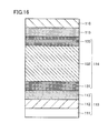
- FIG. 1 is a cross-sectional view showing a configuration of an integrated photoelectric conversion device according to Embodiment 1 of the present invention. As shown in FIG. 1, in the integrated photoelectric conversion device according to Embodiment 1 of the present invention, a photoelectric conversion layer 10 and a reflective layer 17 are laminated on a base material 11 in this order.
- the base material 11 includes a translucent substrate 11a and a first conductive layer 11b formed on the translucent substrate 11a.
- a translucent substrate 11a a glass plate, a translucent resin plate having heat resistance such as polyimide or polyvinyl, and a laminate thereof are preferably used.
- the material of the translucent substrate 11a is not particularly limited as long as it has high light transmissivity and can structurally support the entire photoelectric conversion device. Further, the surface of the translucent substrate 11a may be covered with a metal film, a translucent conductive film, an insulating film, or the like.
- the first conductive layer 11b is made of a transparent conductive material.
- the 1st conductive layer 11b what laminated
- a known method such as a sputtering method, a CVD (Chemical Vapor Deposition) method, an electron beam evaporation method, a sol-gel method, a spray method, and an electrodeposition method can be used.
- an uneven shape is formed on the surface of the first conductive layer 11b. This uneven shape can scatter and refract incident light incident from the translucent substrate 11a side, thereby extending the optical path length, increasing the light confinement effect in the photoelectric conversion layer 10 and increasing the short-circuit current density. .
- a method of forming a concavo-convex shape on the surface of the first conductive layer 11b after forming the first conductive layer 11b on the translucent substrate 11a, a method of forming the concavo-convex shape by mechanical processing such as etching or sand blasting, A method of using the uneven surface shape formed by crystal growth of the film material when forming the first conductive layer 11b, or a regular uneven surface shape is formed because the crystal growth surface is oriented. You may use the method of using what is done.
- tin oxide is deposited on a soda glass by a CVD method (trade name: Asahi-, manufactured by Asahi Glass Co., Ltd.).
- Asahi- manufactured by Asahi Glass Co., Ltd.
- zinc oxide deposited by sputtering or titanium dioxide deposited by sputtering and zinc oxide deposited by sputtering is used.
- the p-type semiconductor layer 12, the i-type semiconductor layer 13, and the n-type semiconductor layer 14 are laminated
- each semiconductor layer is not particularly limited, but the thickness of the p-type semiconductor layer 12 is 5 nm to 50 nm, the thickness of the i-type semiconductor layer 13 is 100 nm to 5000 nm, and the n-type semiconductor layer 14
- the film thickness is preferably 5 nm or more and 100 nm or less. More preferably, the p-type semiconductor layer 12 has a thickness of 10 nm to 30 nm, the i-type semiconductor layer 13 has a thickness of 200 nm to 4000 nm, and the n-type semiconductor layer 14 has a thickness of 10 nm to 30 nm.
- the main material of the constituent material of the photoelectric conversion layer 10 is silicon, and amorphous silicon or microcrystalline silicon is particularly preferable.
- amorphous silicon and microcrystalline silicon include “hydrogenated amorphous silicon” and “hydrogenated microcrystalline silicon”, which are generally used in the art.
- the p-type semiconductor layer 12 is a silicon layer doped with a p-type conductivity determining element.
- a p-type conductivity determining element impurity atoms such as boron, aluminum and gallium can be used.
- the main material of the p-type semiconductor layer 12 may be amorphous silicon or microcrystalline silicon.
- the p-type semiconductor layer 12 includes a crystalline silicon phase because high conductivity can be obtained, the series resistance of the photoelectric conversion layer 10 can be reduced, and the curve factor of the photoelectric conversion device can be increased to obtain high conversion efficiency.
- the p-type semiconductor layer 12 including a crystalline silicon phase is excellent as an underlayer for crystallization of the i-type semiconductor layer 13.
- the p-type semiconductor layer 12 containing a crystalline silicon phase makes it easy to grow a crystal component at the initial stage of the formation of the i-type semiconductor layer 13, and the high-quality i-type semiconductor layer 13 having a high crystallization rate. Enables film formation. Therefore, the p-type semiconductor layer 12 including the crystalline silicon phase contributes to improvement of conversion efficiency by increasing the short-circuit current density of the photoelectric conversion device.
- the p-type semiconductor layer 12 preferably contains carbon atoms or nitrogen atoms as impurities.
- the open-circuit voltage of the photoelectric conversion device can be increased and the conversion efficiency can be improved as compared with a photoelectric conversion device having a p-type semiconductor layer that does not contain the impurities. .
- the impurity concentration is low.
- the impurity concentration is low, the occurrence of discontinuity or mismatch of the band gap between the p-type semiconductor layer 12 and the i-type semiconductor layer 13 is reduced, so there is no need to provide an interface layer or the like between both layers.
- a photoelectric conversion device with high conversion efficiency can be obtained easily and inexpensively.
- the p-type semiconductor layer 12 consists of a microcrystalline silicon layer containing a trace amount of carbon. Note that the p-type semiconductor layer 12 may contain impurities of both carbon atoms and nitrogen atoms.
- the i-type semiconductor layer 13 is a microcrystalline silicon layer to which no impurity is added.
- the i-type semiconductor layer 13 may contain a small amount of an impurity element as long as it is a substantially intrinsic semiconductor.
- amorphous silicon may be used as the material of the i-type semiconductor layer 13 instead of microcrystalline silicon.
- microcrystalline silicon is preferable to amorphous silicon as a material for the i-type semiconductor layer 13 in that high photoelectric conversion efficiency can be obtained because photodegradation does not occur.
- i is reduced in order to reduce recombination at the interface between the n-type semiconductor layer 14 and the i-type semiconductor layer 13.
- the type semiconductor layer 13 is preferably microcrystalline silicon.
- the i-type semiconductor layer 13 may contain at least one of amorphous silicon germanium and microcrystalline silicon germanium.
- the atomic composition percentage of germanium in the i-type semiconductor layer 13 is preferably 5 atom% or more and 30 atom% or less.
- the band gap is hardly reduced, and therefore the short circuit current density of the photoelectric conversion device cannot be increased, which is not preferable.
- the atomic composition percentage of germanium exceeds 30 atomic%, the band gap decreases and the open circuit voltage of the photoelectric conversion device decreases, or the crystal grain size of the i-type semiconductor layer 13 decreases and the conversion efficiency of the photoelectric conversion device is reduced. Is unfavorable because of lowering.
- the n-type semiconductor layer 14 is a silicon layer doped with an n-type conductivity determining element.
- impurity atoms such as phosphorus, nitrogen and oxygen can be used.
- the main material of the n-type semiconductor layer 14 may be amorphous silicon or microcrystalline silicon. It is preferable that the n-type semiconductor layer 14 includes crystalline silicon because high conductivity can be obtained, the series resistance of the photoelectric conversion layer 10 can be reduced, and the conversion factor of the photoelectric conversion device can be increased to obtain high conversion efficiency.
- the n-type semiconductor layer 14 preferably contains carbon atoms or nitrogen atoms as impurities.
- the conversion efficiency can be improved by increasing the open-circuit voltage of the photoelectric conversion device as compared with a photoelectric conversion device having an n-type semiconductor layer not containing the impurities. .
- the n-type semiconductor layer 14 is made of microcrystalline silicon. Note that the n-type semiconductor layer 14 may contain impurities of both carbon atoms and nitrogen atoms.
- the silicon carbide crystal phase is not substantially contained.
- This state can be confirmed by, for example, that when a Raman scattering spectrum of microcrystalline silicon containing carbon atoms is observed, a peak attributed to a silicon-carbon bond constituting the silicon carbide crystal is not substantially detected. it can.
- This state can also be confirmed by substantially not detecting a diffraction peak attributed to the silicon carbide crystal structure in the X-ray diffraction method.
- a CVD method can be used as a method for forming the photoelectric conversion layer 10.
- the CVD method include atmospheric pressure CVD, reduced pressure CVD, plasma CVD, thermal CVD, hot wire CVD, and MOCVD (Metal Organic Chemical Vapor Deposition) method.
- the plasma CVD method is used.
- the silicon-containing gas used when forming the photoelectric conversion layer 10 by the plasma CVD method is not particularly limited as long as it contains silicon atoms such as SiH 4 and Si 2 H 6, but generally SiH 4 is used. .
- H 2 gas As a dilution gas used together with the silicon-containing gas, H 2 gas, Ar gas, and He gas can be used, but H 2 gas is generally used when forming amorphous silicon and microcrystalline silicon.
- a doping gas is used together with the silicon-containing gas and the dilution gas.
- the doping gas is not particularly limited as long as it contains a target type conductivity determining element.
- the p-type conductivity determining element is boron
- B 2 H 6 is used as the n-type conductivity.
- PH 3 is used when the sex determining element is phosphorus.
- the abundance ratio between the amorphous phase and the crystalline phase is controlled by appropriately controlling the film forming parameters such as the substrate temperature, pressure, gas flow rate, and power input to the plasma. It is possible to control.
- the 2nd conductive layer 15 and the back surface electrode 16 are laminated
- the second conductive layer 15 functions as an electrode, so that the current generated by the photoelectric conversion layer 10 can be taken out. Moreover, when the back surface electrode 16 mentioned later is formed, the 2nd conductive layer 15 can aim at the improvement of the light confinement effect with respect to incident light, and the improvement of a light reflectivity. Furthermore, by forming the second conductive layer 15, it is possible to prevent the elements contained in the back electrode 16 from diffusing into the photoelectric conversion layer 10.
- the second conductive layer 15 is formed by the same material and manufacturing method as the first conductive layer 11b.
- the thickness of the 2nd conductive layer 15 should just be 20 nm or more.
- the thickness of the second conductive layer 15 is preferably 20 nm or more and 3000 nm or less.
- the back surface electrode 16 should just be comprised by the at least 1 or more layers of conductive layer, and the light reflectivity and electrical conductivity of a conductive layer are so preferable that it is high.
- a material for the back electrode 16 a metal material such as silver, aluminum, titanium and palladium, or an alloy thereof, which has high visible light reflectivity, can be used.
- the back electrode 16 is formed on the photoelectric conversion layer 10 by a CVD method, a sputtering method, a vacuum evaporation method, an electron beam evaporation method, a spray method, a screen printing method, or the like.
- the back electrode 16 reflects light that has not been absorbed in the photoelectric conversion layer 10 and returns it to the photoelectric conversion layer 10, which contributes to improvement in conversion efficiency of the photoelectric conversion device.
- the thickness of the back electrode 16 is preferably 100 nm or more and 400 nm or less. Note that the back electrode 16 is not necessarily provided.
- FIG. 2 is a cross-sectional view showing the configuration of the integrated photoelectric conversion device according to Comparative Example 1.
- an integration process for connecting photoelectric conversion unit elements in series is performed as follows.
- a region separation groove 50 is formed in the first conductive layer 11b provided on the translucent substrate 11a, and the first conductive layer 11b is divided into a plurality of regions.
- the photoelectric conversion layer 10 is provided over the two first conductive layers 11b adjacent to each other on the first conductive layer 11b.
- a connecting groove 80 having the upper surface of the first conductive layer 11b as a bottom surface is formed. That is, the connecting groove 80 is formed from the upper surface of the photoelectric conversion layer 10 to the upper surface of the first conductive layer 11b.
- the second conductive layer 15 is provided on the photoelectric conversion layer 10 and along the inner wall of the connecting groove 80.
- the back electrode 16 that is electrically connected to the adjacent first conductive layer 11b via the connection groove 80 is provided on the second conductive layer 15. In this way, the first conductive layer 11b and the back electrode 16 are electrically connected.
- an element isolation groove 70 that divides the photoelectric conversion layer 10 and the reflection layer 17 is formed.
- a plurality of photoelectric conversion unit elements electrically connected in series with each other are formed.
- the method for forming the region separating groove 50 and the connecting groove 80 is not particularly limited as long as the material constituting the first conductive layer 11b and the photoelectric conversion layer 10 can be removed.
- a wet etching method using a chemical, RIE (reactive ion etching), or a dry etching method such as laser scribing can be used.
- a laser scribing method that can dry and process materials without using a vacuum apparatus is preferable.
- a laser beam is incident from the translucent substrate 11a side using a laser scribing method to form a groove.
- the wavelength of the laser light used in the laser scribing method is YAG (Yttrium Aluminum Garnet) 1064 nm (hereinafter referred to as IR laser light) and its second harmonic, SHG 532 nm (hereinafter referred to as SHG laser light). .
- IR laser light Yttrium Aluminum Garnet
- SHG laser light SHG 532 nm
- IR laser light is absorbed by the first conductive layer 11b.
- the first conductive layer 11b is excited by IR laser light to generate heat, and the first conductive layer 11b itself and a layer deposited on the first conductive layer 11b are removed by an ablation effect.
- the SHG laser light is hardly absorbed by the first conductive layer 11b, and most of it is absorbed by the photoelectric conversion layer 10.
- the photoelectric conversion layer 10 is excited by the SHG laser light to generate heat, and the photoelectric conversion layer 10 itself and the layer deposited on the photoelectric conversion layer 10 are removed by the ablation effect.
- the region separation groove 50 is formed using IR laser light
- the connection groove 80 and the element separation groove 70 are formed using SHG laser light.
- the integration process of the present embodiment is different from the integration process of Comparative Example 1 in that the connecting groove 60 is formed using IR laser light. That is, the region separation groove 50 and the connection groove 60 are formed using IR laser light, and the element separation groove 70 is formed using SHG laser light.
- the connecting groove portion 60 By forming the connecting groove portion 60 using IR laser light, as shown in FIG. 1, the connecting groove portion 60 whose bottom surface is the upper surface of the translucent substrate 11a can be formed. That is, the connecting groove 60 is formed from the upper surface of the photoelectric conversion layer 10 to the upper surface of the translucent substrate 11a.
- the connecting groove 80 is formed by SHG laser light as in Comparative Example 1, the connecting groove 80 is formed by removing the photoelectric conversion layer 10 by the ablation effect as described above.
- the ablation effect is greatly influenced by the hydrogen concentration in the silicon. Specifically, the higher the hydrogen concentration in the silicon, the easier it is to obtain the ablation effect and the better the connecting groove 80 can be formed. This is because the silicon-hydrogen bond is broken by the energy of the SHG laser light absorbed in the photoelectric conversion layer 10 and hydrogen is suddenly generated in the film, and the silicon film is destroyed when the hydrogen is desorbed. Conceivable.
- the factor that determines whether or not the connection groove 80 can be formed by the SHG laser light is the hydrogen concentration of the i-type semiconductor layer.
- the hydrogen concentration of an i-type semiconductor layer containing microcrystalline silicon is lower than that of an i-type semiconductor layer made of only amorphous silicon. This is because the crystalline silicon contained in the microcrystalline silicon has a crystal structure composed of silicon-silicon.
- the hydrogen concentration in silicon is further reduced. This is because germanium-hydrogen bonds are less likely to be formed than silicon-hydrogen bonds. Due to the above factors, it has been difficult to form the connecting groove 80 in the photoelectric conversion layer 10 including the i-type semiconductor layer having a relatively low hydrogen concentration by using SHG laser light.
- the connecting groove 60 is formed using IR laser light as in the present embodiment, the ablation effect by IR laser light is generated in the first conductive layer 11b. Therefore, it is possible to satisfactorily form the connecting groove 60 without depending on the hydrogen concentration in silicon in the i-type semiconductor layer and the material of the i-type semiconductor layer.
- the IR laser light used for forming the connecting groove 60 can be the same laser light as the IR laser light used for forming the region separating groove 50. Therefore, since existing equipment can be used as it is, an increase in manufacturing cost can be suppressed.
- IR laser light and SHG laser light are often irradiated with pulses at an appropriate frequency, for example, at a frequency of 5 kHz to 30 kHz.
- the scanning speed of the laser light is appropriately adjusted so that the traces from which the layer has been removed by laser light irradiation have a continuous groove shape.
- the scanning speed is generally in the range of 50 mm / second to 1000 mm / second.
- the above-mentioned parameters such as the pulse frequency of the laser beam, the shape and width of the irradiation trace, and the scanning speed are appropriately selected.
- the output of the laser light is about 8 W to 15 W for IR laser light and about 0.1 W to 0.5 W for SHG laser light at the average power in the pulse output state.
- the appropriate output of the laser light varies depending on the film thickness or adhesion strength of the irradiation object and the scanning speed of the laser light, and therefore is appropriately selected in consideration of the state of the irradiation object after the laser light irradiation.
- the output of IR laser light is 13 W
- the output of SHG laser light is 0.3 W.
- the connecting groove 60 formed as described above has an inner wall 11c formed by removing the first conductive layer 11b.
- the inner wall 11 c is a cut surface of the bulk body of the first conductive layer 11 b that appears due to the formation of the connecting groove 60. Therefore, the inner wall 11c is not in contact with outside air, cleaning water or other contaminants before the connection groove portion 60 is formed, and is not deteriorated.
- the bottom surface of the connecting groove 80 is the upper surface of the first conductive layer 11b, and before forming the connecting groove 80, the outside air, cleaning water and other contaminants In contact therewith, foreign matter or contaminants having a changed composition adhere to the bottom surface of the connecting groove 80.
- the first conductive layer 11b is brought into contact with the first conductive layer 11b and the second conductive layer 15 on the inner wall 11c of the connection groove 60 as shown in FIG.
- the electrical resistance due to the foreign matter or contaminants can be reduced.
- a decrease in photoelectric conversion efficiency due to an increase in series connection resistance of a plurality of photoelectric conversion unit elements can be suppressed.
- the photoelectric conversion layer 10 existing on the first conductive layer 11b is completely removed. Therefore, the remainder of the photoelectric conversion layer 10 does not intervene between the first conductive layer 11b and the second conductive layer 15, and good electrical connection can be realized also from this viewpoint.
- Embodiment 2 of the present invention an integrated photoelectric conversion device and a manufacturing method thereof according to Embodiment 2 of the present invention will be described. Since the integrated photoelectric conversion device according to the present embodiment is different from the integrated photoelectric conversion device according to Embodiment 1 only in including an antireflection layer, the description of the other components will not be repeated.
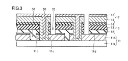
- FIG. 3 is a cross-sectional view showing a configuration of an integrated photoelectric conversion device according to Embodiment 2 of the present invention.
- FIG. 4 is a cross-sectional view showing the configuration of the integrated photoelectric conversion device according to Comparative Example 2.
- the antireflection layer 11 d is formed between the first conductive layer 11 b and the photoelectric conversion layer 10.
- the refractive index of the antireflection layer 11 d is preferably a value between the refractive index of the first conductive layer 11 b and the refractive index of the photoelectric conversion layer 10.
- the refractive index of the antireflection layer 11d is preferably 2.0 or more and 3.0 or less.
- the thickness of the antireflection layer 11d is preferably 30 nm or more and 100 nm or less.
- the appropriate thickness of the antireflection layer 11d varies depending on the balance with the refractive index of the antireflection layer 11d and the wavelength range of light for which antireflection is desired.
- the antireflection layer 11d may be insulative when formed to be relatively thin, but may have conductivity from the viewpoint of improving the electrical contact between the photoelectric conversion layer 10 and the substrate 11. desirable.
- the antireflection layer 11d may be a single layer or a multilayer film having a single refractive index, or may be a single layer or a plurality of layers having different refractive indexes in the film thickness direction formed by a method such as a composition gradient method. You may be comprised by the laminated film which consists of layers.
- the antireflection layer 11d As a method for forming the antireflection layer 11d, known methods such as a sputtering method, a CVD method, an electron beam evaporation method, a sol-gel method, a spray method, and an electrodeposition method can be used. Further, similarly to the first conductive layer 11b, it is preferable that an uneven shape is formed on the surface of the antireflection layer.
- the same means as the first conductive layer 11b can be used, but by forming the antireflection layer 11d on the uneven shape of the first conductive layer 11b.
- the surface of the antireflection layer 11d may have a concavo-convex shape following the concavo-convex shape of the first conductive layer 11b.
- the antireflection layer 11d can be formed by sputtering or the like because the antireflection layer 11d can be prevented from being damaged by plasma when the photoelectric conversion layer 10 is formed later.
- connection groove 80 by forming the connection groove 80 using SHG laser light, as shown in FIG. 4, the connection groove 80 having the upper surface of the antireflection layer 11d as the bottom surface is formed. That is, the connecting groove 80 is formed from the upper surface of the photoelectric conversion layer 10 to the upper surface of the antireflection layer 11d.
- the first conductive layer 11b and the second conductive layer 15 are in contact with each other through the antireflection layer 11d.
- the electrical connection of the plurality of photoelectric conversion unit elements is deteriorated, the series resistance is increased, the curve factor of the integrated photoelectric conversion device is decreased, and the conversion efficiency is decreased.
- the connecting groove 60 by forming the connecting groove 60 using IR laser light, as shown in FIG. 3, the connecting groove 60 having the upper surface of the translucent substrate 11a as the bottom surface can be formed. it can. That is, the connecting groove 60 is formed from the upper surface of the photoelectric conversion layer 10 to the upper surface of the translucent substrate 11a.
- the connecting groove 60 formed as described above has an inner wall 11c formed by removing the first conductive layer 11b.
- the inner wall 11 c is a cut surface of the bulk body of the first conductive layer 11 b that appears due to the formation of the connecting groove 60. Therefore, the inner wall 11c is not in contact with outside air, cleaning water or other contaminants before the connection groove portion 60 is formed, and is not deteriorated.
- the first conductive layer 11b and the second conductive layer 15 are in contact with each other without passing through the antireflection layer 11d.
- the photoelectric conversion efficiency is improved by the antireflection layer 11d, the decrease in the photoelectric conversion efficiency due to the increase in the series connection resistance of the plurality of photoelectric conversion unit elements is suppressed. it can.
- Embodiment 3 of the present invention Since the integrated photoelectric conversion device according to this embodiment is different from the integrated photoelectric conversion device according to Embodiment 1 only in that it is a tandem type, the description of other configurations will not be repeated.
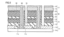
- FIG. 5 is a cross-sectional view showing a configuration of an integrated photoelectric conversion device according to Embodiment 3 of the present invention.
- FIG. 6 is a cross-sectional view showing the configuration of the integrated photoelectric conversion device according to Comparative Example 3.
- the tandem integrated photoelectric conversion device includes first and second photoelectric conversion layers 10 and 20.
- a p-type semiconductor layer 22 In the second photoelectric conversion layer 20, a p-type semiconductor layer 22, an i-type semiconductor layer 23, and an n-type semiconductor layer 24 are stacked in order from the base material 11 side to form a pin junction.
- the pin junction closest to the light incident side is often referred to as the top cell, and the pin junction farthest from the light incident side is often referred to as the bottom cell.
- the pin junction located between the top cell and the bottom cell is often referred to as a middle cell.
- the tandem integrated photoelectric conversion device according to the present embodiment and comparative embodiment 3 is a photoelectric conversion device having a super straight type structure.
- the first photoelectric conversion layer 10, the second photoelectric conversion layer 20, and the reflection layer 17 are laminated on the base material 11 in this order.
- the first photoelectric conversion layer 10 Since the first photoelectric conversion layer 10 is located on the light incident side, only the light transmitted through the first photoelectric conversion layer 10 is incident on the second photoelectric conversion layer 20. Therefore, in the tandem integrated photoelectric conversion device, the first and second photoelectric conversion layers 10 and 20 can receive different spectral regions of the incident light, so that the light use efficiency can be improved.
- a high open-circuit voltage substantially equal to the sum of the open-circuit voltages of the two photoelectric conversion layers 10 and 20 can be obtained.
- the band gap of the first photoelectric conversion layer 10 located on the light incident side larger than the band gap of the second photoelectric conversion layer 20
- short wavelength light of the incident light is mainly used for the first photoelectric conversion layer. Since the long wavelength light is mainly absorbed by the second photoelectric conversion layer 20 in the conversion layer 10, the conversion efficiency of the tandem integrated photoelectric conversion device can be further improved.
- silicon-based materials having different band gaps include amorphous silicon carbide, amorphous silicon, amorphous silicon germanium, amorphous germanium, microcrystalline silicon, microcrystalline silicon germanium, and microcrystalline germanium. These can be appropriately selected and used as the light absorption layer.
- amorphous silicon having a large band gap absorbs light in the short wavelength region of the incident light.
- microcrystalline silicon having a small band gap is designed to absorb the remaining light in the long wavelength region.
- Microcrystalline silicon and microcrystalline silicon germanium are known not to cause photodegradation as described above, and are generally preferred for use as materials that absorb light of long wavelengths in multi-junction thin-film silicon solar cells. It has been.
- the first and second photoelectric conversion layers 10 and 20 it is only necessary that the stacking directions of the pin junctions are the same and that the p-type semiconductor layers 12 and 22 are positioned on the light incident side. The same applies when there are three or more photoelectric conversion layers. That is, when the first photoelectric conversion layer 10 has a pin junction, the second photoelectric conversion layer 20 also has a pin junction, and when the first photoelectric conversion layer 10 has a nip junction, the second photoelectric conversion layer. 20 also has a nip junction.
- each semiconductor layer in the first and second photoelectric conversion layers 10 and 20 is not particularly limited, but in the first photoelectric conversion layer 10, the thickness of the p-type semiconductor layer 12 is 5 nm or more.
- the film thickness of the i-type semiconductor layer 13 is preferably 100 nm to 500 nm and the film thickness of the n-type semiconductor layer 14 is preferably 5 nm to 50 nm. More preferably, the p-type semiconductor layer 12 has a thickness of 10 nm to 30 nm, the i-type semiconductor layer 13 has a thickness of 200 nm to 400 nm, and the n-type semiconductor layer 14 has a thickness of 10 nm to 30 nm.
- the p-type semiconductor layer 22 has a thickness of 5 nm to 50 nm
- the i-type semiconductor layer 23 has a thickness of 1000 nm to 5000 nm
- the n-type semiconductor layer 24 has a thickness of 5 nm to 100 nm.
- the following is preferable. More preferably, the p-type semiconductor layer 22 has a thickness of 10 nm to 30 nm
- the i-type semiconductor layer 23 has a thickness of 2000 nm to 4000 nm
- the n-type semiconductor layer 24 has a thickness of 10 nm to 30 nm.
- An intermediate layer may be formed between at least one pair of adjacent pin junctions or nip junctions among a plurality of pin junctions or a plurality of nip junctions. That is, an intermediate layer may be formed between the first photoelectric conversion layer 10 and the second photoelectric conversion layer 20. When there are three or more photoelectric conversion layers, an intermediate layer may be formed in at least one place between the photoelectric conversion layers.
- the intermediate layer is preferably composed of a light-transmitting conductive film.
- the intermediate layer By providing the intermediate layer, a part of the light that has passed through the first photoelectric conversion layer 10 and is incident on the intermediate layer is reflected by the intermediate layer, and the rest is transmitted through the intermediate layer to the second photoelectric conversion layer 20. Since the light enters, the amount of light incident on each photoelectric conversion layer can be controlled.
- the value of the photocurrent in the first and second photoelectric conversion layers 10 and 20 can be equalized.
- the photogenerated carriers generated in the first and second photoelectric conversion layers 10 and 20 it is possible to increase the short-circuit current value of the tandem integrated photoelectric conversion device and improve the conversion efficiency.
- the connecting groove 60 has an inner wall 11c formed by removing the first conductive layer 11b.
- the inner wall 11 c is a cut surface of the bulk body of the first conductive layer 11 b that appears due to the formation of the connecting groove 60. Therefore, the inner wall 11c is not in contact with outside air, cleaning water or other contaminants before the connection groove portion 60 is formed, and is not deteriorated.
- connection groove portion 60 can be reliably formed in the tandem integrated photoelectric conversion device by increasing the overlap of the laser light irradiation areas without increasing the output of the IR laser light.
- the bottom surface of the connecting groove 80 is the upper surface of the first conductive layer 11b, and before forming the connecting groove 80, the outside air and cleaning water and other contaminants In contact therewith, foreign matter or contaminants having a changed composition adhere to the bottom surface of the connecting groove 80.
- the output of the SHG laser light necessary for forming the connecting groove 80 strongly depends on the concentration of hydrogen contained in the first and second photoelectric conversion layers 10 and 20.
- amorphous silicon is formed on the light incident side, and this amorphous silicon contains a relatively large amount of hydrogen. Therefore, if the output of the SHG laser light is about 0.2 W or more and 0.6 W or less, the connecting groove 80 can be reliably formed in the tandem integrated photoelectric conversion device.
- the first conductive layer 11 b and the second conductive layer 15 are brought into contact with each other on the inner wall 11 c of the connection groove portion 60, whereby the first conductive layer 11 b is formed on the bottom surface of the connection groove portion 80 as shown in FIG. 6.
- the electrical resistance due to the foreign matter or contaminants can be reduced.
- a decrease in photoelectric conversion efficiency due to an increase in series connection resistance of a plurality of photoelectric conversion unit elements can be suppressed.
- Embodiment 4 of the present invention Since the integrated photoelectric conversion device according to this embodiment is different from the tandem integrated photoelectric conversion device according to Embodiment 3 only in that an antireflection layer is provided, the description of other configurations will not be repeated.
- FIG. 7 is a cross-sectional view showing a configuration of an integrated photoelectric conversion device according to Embodiment 4 of the present invention.
- FIG. 8 is a cross-sectional view showing a configuration of an integrated photoelectric conversion device according to Comparative Example 4.
- the amount of incident light on the first and second photoelectric conversion layers 10 and 20 is increased, and more In order to increase the short-circuit current density, an antireflection layer 11 d is formed between the first conductive layer 11 b and the first photoelectric conversion layer 10.
- the connecting groove 80 is formed by using SHG laser light, thereby forming the connecting groove 80 having the upper surface of the antireflection layer 11d as the bottom as shown in FIG. That is, the connecting groove 80 is formed from the upper surface of the second photoelectric conversion layer 20 to the upper surface of the antireflection layer 11d.
- the first conductive layer 11b and the second conductive layer 15 are in contact with each other through the antireflection layer 11d.
- the electrical connection of the plurality of photoelectric conversion unit elements is deteriorated, the series resistance is increased, the curve factor of the integrated photoelectric conversion device is decreased, and the conversion efficiency is decreased.
- connection groove 60 by forming the connection groove 60 using IR laser light, as shown in FIG. 7, the connection groove 60 having the upper surface of the translucent substrate 11a as the bottom surface can be formed. it can. That is, the connecting groove 60 is formed from the upper surface of the second photoelectric conversion layer 20 to the upper surface of the translucent substrate 11a.
- the connecting groove 60 formed as described above has an inner wall 11c formed by removing the first conductive layer 11b.
- the inner wall 11 c is a cut surface of the bulk body of the first conductive layer 11 b that appears due to the formation of the connecting groove 60. Therefore, the inner wall 11c is not in contact with outside air, cleaning water or other contaminants before the connection groove portion 60 is formed, and is not deteriorated.
- the first conductive layer 11b and the second conductive layer 15 are in contact with each other without passing through the antireflection layer 11d.
- the photoelectric conversion efficiency is improved by the antireflection layer 11d, and the decrease in the photoelectric conversion efficiency due to the increase in the series connection resistance of the plurality of photoelectric conversion unit elements. Can be suppressed.
- Example 1 In Example 1, the super straight type photoelectric conversion device shown in FIG. 1 was produced as follows.
- a blue plate glass (Asahi Glass Co., Ltd.) having a length of 115 mm ⁇ width of 115 mm ⁇ thickness of 3.9 mm, in which a first conductive layer 11 b made of a tin oxide-based transparent conductive film is formed on the surface of a translucent substrate 11 a.
- Zinc oxide was deposited on the base material 11 by sputtering.
- the substrate 11 was irradiated with an IR laser beam in a straight line to form a region separation groove 50 for separating the first conductive layer 11b into a strip shape.
- the laser processing conditions at this time were a laser output current of 90%, a laser transmission frequency of 25 kHz, and a scanning speed of 600 mm / second.
- the first conductive layer 11b was divided into strips having a width of 10.260 mm by the region separation grooves 50 having a width of 60 ⁇ m. In this state, when a tester was applied on the two first conductive layers 11b so as to straddle the region separation groove 50, insulation was confirmed, and a resistance value of several M ⁇ or more was obtained. From this, it was confirmed that each of the plurality of strip-like regions was electrically insulated reliably.
- the p-type semiconductor layer 12, the i-type semiconductor layer 13, and the n-type semiconductor layer 14 were sequentially laminated by the plasma CVD method under the conditions described later to form the photoelectric conversion layer 10.
- Each layer of the photoelectric conversion layer 10 was formed under the following conditions.
- a mixed gas containing SiH 4 , H 2 and B 2 H 6 was used as a source gas.
- the gas flow ratio of H 2 to SiH 4 was 150 times, and the gas flow ratio of B 2 H 6 to SiH 4 was 0.003 times.
- the p-type semiconductor layer 12 is desirably thin as long as it does not impair the function as the p-type semiconductor layer in order to increase the amount of light incident on the i-type semiconductor layer 13 that is a photoactive layer.
- the film thickness was taken.
- the i-type semiconductor layer 13 For the formation of the i-type semiconductor layer 13, a mixed gas containing SiH 4 and H 2 was used as a source gas. The gas flow ratio of H 2 to SiH 4 was 80 times. In this example, the film thickness of the i-type semiconductor layer 13 was 2500 nm.
- a mixed gas containing SiH 4 , H 2 , PH 3 and N 2 was used as a source gas.
- the gas flow ratio of H 2 to SiH 4 was 100 times, and the gas flow ratio of PH 3 to SiH 4 was 0.03 times.
- the film thickness of the n-type semiconductor layer 14 is preferably as thin as not to impair the function as the n-type semiconductor layer in order to suppress absorption of reflected light from the back electrode 16. In this embodiment, the film thickness is 20 nm. did.
- the substrate temperature at the time of forming the p-type, i-type and n-type semiconductor layers 12, 13, and 14 by plasma CVD was set to 180 ° C.
- FIG. 9 is a cross-sectional view showing a state in which a photoelectric conversion layer is provided in Example 1. Through the above steps, a structure 300 as shown in FIG. 9 was formed.
- connection groove 60 was formed by irradiating the structure 300 with IR laser light in a straight line.
- the laser processing conditions at this time were the same as the laser processing conditions of the region separation groove 50.
- FIG. 10 is a cross-sectional view showing a state in which connection grooves are formed in the first embodiment.
- the structure 400 as shown in FIG. 10 was formed by the above steps.
- the width of the connecting groove 60 was 60 ⁇ m.
- the center-to-center distance between the connecting groove 60 and the region separating groove 50 was 100 ⁇ m.
- FIG. 11 is a cross-sectional view illustrating a state where a reflective layer is formed in the first embodiment. Through the above steps, a structure 500 as shown in FIG. 11 was formed.
- the element isolation groove 70 was formed by irradiating the structure 500 with SHG laser light in a straight line.
- the laser processing conditions at this time were a laser output current of 85%, a laser transmission frequency of 25 kHz, and a scanning speed of 800 mm / second.
- the width of the element isolation trench 70 was 60 ⁇ m.
- the center-to-center distance between the element isolation trench 70 and the connection trench 60 was 100 ⁇ m.
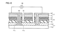
- Example 1 obtained integrated photoelectric conversion device, AM 1.5, under the conditions of irradiance 100 mW / cm 2, current cell area 1 cm 2 - voltage characteristics were measured.
- FIG. 12 is a cross-sectional view showing a state in which a resistance measuring device is connected in the first embodiment. As shown in FIG. 12, the resistance measuring device 90 was connected on the back surface electrode 16 through the serial connection part.
- Example 1 the resistance value of the series connection portion is 3 ⁇ , the short-circuit current density is 22.6 mA / cm 2 , the open circuit voltage is 0.510 V, the fill factor is 0.714, the series resistance is 6 ⁇ , and the conversion efficiency is 8.2. %Met.
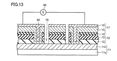
- Comparative Example 1 a super straight type integrated photoelectric conversion device was manufactured under the same conditions as in Example 1 except that the connecting groove 80 was formed using SHG laser light.
- FIG. 13 is a cross-sectional view showing a state in which a resistance measuring device is connected in Comparative Example 1. As shown in FIG. 13, the resistance measuring device 90 was connected on the back surface electrode 16 via the serial connection part.
- the resistance value of the series connection portion is 10 ⁇
- the short-circuit current density is 22.6 mA / cm 2
- the open circuit voltage is 0.511V
- the fill factor is 0.659
- the series resistance is 10 ⁇
- the conversion efficiency is 7.6. %Met.
- Example 2 On the base material 11, titanium dioxide is deposited to a thickness of 70 nm as an antireflection layer 11 d by sputtering, and further zinc oxide is deposited to a thickness of 10 nm as a protective film for the antireflection layer by sputtering. I let you. A super straight type integrated photoelectric conversion device was manufactured under the same conditions as in Example 1 except for the above.
- FIG. 14 is a cross-sectional view showing a state in which a resistance measuring device is connected in the second embodiment. As shown in FIG. 14, the resistance measuring device 90 was connected on the back surface electrode 16 through the serial connection part.
- Example 2 the resistance value of the series connection part is 3 ⁇ , the short-circuit current density is 23.1 mA / cm 2 , the open circuit voltage is 0.512V, the fill factor is 0.715, the series resistance is 6 ⁇ , and the conversion efficiency is 8.5. %Met.
- a photoelectric conversion device was manufactured under the following conditions.
- Comparative Example 2 a super straight type integrated photoelectric conversion device was manufactured under the same conditions as in Example 2 except that the connecting groove 80 was formed using SHG laser light.
- Photoelectric conversion device of Comparative Example 2 AM 1.5, under the conditions of irradiance 100 mW / cm 2, current cell area 1 cm 2 - voltage characteristics were measured.
- FIG. 15 is a cross-sectional view showing a state in which a resistance measuring device is connected in Comparative Example 2. As shown in FIG. 15, the resistance measuring device 90 was connected on the back surface electrode 16 through the serial connection part.
- the resistance value of the series connection portion is 500 ⁇
- the short-circuit current density is 7.39 mA / cm 2
- the open circuit voltage is 0.161 V
- the fill factor is 0.245
- the series resistance is 25 ⁇
- the conversion efficiency is 0.31. %Met.
- Table 1 summarizes the experimental results of Examples 1 and 2 and Comparative Examples 1 and 2.
- the integrated photoelectric conversion devices of Examples 1 and 2 were able to suppress a decrease in photoelectric conversion efficiency due to an increase in series connection resistance, compared to the integrated photoelectric conversion devices of Comparative Examples 1 and 2.
- the resistance of the series connection portion was equivalent to that of the integrated photoelectric conversion device of Example 1. Therefore, the fill factor of the integrated photoelectric conversion device of Example 2 is also equivalent to that of the integrated photoelectric conversion device of Example 1.
- FIG. 16 is sectional drawing which shows the structure of the solar cell which concerns on Embodiment 5 of this invention.
- the solar cell according to the present embodiment is a super straight type in which light enters from the substrate 110 side, and the light-transmitting substrate 111, the first conductive film 112, the antireflection layer 113, the photoelectric conversion layer 114, and the second conductive film 115. And the back electrode 116 are laminated in this order.
- the light-transmitting substrate 111, the first conductive film 112, and the antireflection layer 113 constitute a substrate 110.
- the light-transmitting substrate 111 is not particularly limited as long as it has high light transmittance and can structurally support the entire photoelectric conversion layer 114.
- a glass plate, a translucent resin plate having heat resistance such as polyimide or polyvinyl, or a laminate of a glass plate and a translucent resin plate can be used.
- a metal film, a transparent conductive film, an insulating film, or the like may be provided on the surface of the light-transmitting substrate 111.
- the thickness of the translucent substrate 111 is not specifically limited, For example, it is preferable that they are 50 micrometers or more and 10 mm or less.
- the light-transmitting substrate 111 is excellent in light transmittance means, for example, that the transmittance of the light-transmitting substrate 111 is 50% or more in the wavelength region of light absorbed by the photoelectric conversion layer 114, It is preferably 70% or more, more preferably 90% or more. This is also true for the first conductive film 112.
- the first conductive film 112 is preferably provided over the light-transmitting substrate 111.
- the first conductive film 112 is preferably made of a material having a high light transmittance like the light-transmitting substrate 111, and is preferably made of a material having a high electrical conductivity in order to function as an electrode.
- the first conductive film 112 may be a single layer made of ITO, tin oxide, zinc oxide, or the like, or may be configured by stacking single layers.
- a trace amount of impurities is added to the first conductive film 112.
- Examples of the method for forming the first conductive film 112 include known methods such as a sputtering method, a CVD method, an electron beam evaporation method, a sol-gel method, a spray method, and an electrodeposition method.
- the concavo-convex shape for example, after forming the first conductive film 112 on the translucent substrate 111, the concavo-convex shape is formed on the surface of the first conductive film 112 by an etching method or mechanical processing such as sandblasting. Can be formed. Further, when the first conductive film 112 is formed by crystal growth, the uneven shape formed by the crystal growth may be used, or when the first conductive film 112 is formed by orientation growth, the first conductive film 112 is formed on the surface. Regular irregular shapes may be used.
- the antireflection layer 113 is provided on the first conductive film 112 and contains niobium oxide.
- Niobium oxide has a higher refractive index than a material generally used as a material of a transparent conductive film (first conductive film 112) in a solar cell, and is higher than a silicon-based material generally used as a material of a photoelectric conversion layer in a solar cell. Also has a low refractive index.
- the refractive index of niobium oxide in the wavelength region (for example, visible region) of light absorbed by the photoelectric conversion layer 114 is about 2.3, and the material of the first conductive film 112 in the same wavelength region The refractive index is about 2.0, and the refractive index of the silicon-based material constituting the photoelectric conversion layer 114 in the same wavelength region is about 3.5.
- the refractive index means a refractive index in a wavelength region of light absorbed by the photoelectric conversion layer 114.
- the band gap energy of titanium oxide that has been suitably used as an antireflection layer in the past is 3.0 eV for the stable rutile type and 3.2 eV for the unstable anatase type.
- the band gap energy of niobium oxide is about 3.4 eV, which is larger than the band gap energy of titanium oxide.
- niobium oxide is less susceptible to reduction by H species than titanium oxide suitably used as a material for the antireflection layer 113, and has a higher resistance to reduction by H species than titanium oxide. Therefore, an anti-reduction layer (a layer for preventing reduction of the anti-reflection layer 113 by H species) may not be provided between the anti-reflection layer 113 and the photoelectric conversion layer 114.
- the antireflection layer 113 is in contact with the photoelectric conversion layer 114 in view of the fact that it is not necessary to provide an anti-reduction layer separately from the antireflection layer 113.
- the antireflection layer 113 is preferably in contact with each of the first conductive film 112 and the photoelectric conversion layer 114.
- Niobium oxide means a compound of niobium and oxygen, and examples thereof include NbO (mononiobium oxide), NbO 2 (biniobium oxide), and Nb 2 O 5 (penta niobium oxide).
- the antireflection layer 113 may be made of a single niobium oxide or may contain a plurality of types of niobium oxides. When the antireflection layer 113 includes a plurality of types of niobium oxide, it is preferable that the composition ratio of oxygen in the niobium oxide in the antireflection layer 113 is lower on the photoelectric conversion layer 114 side than on the first conductive film 112 side. .
- the refractive index of the antireflection layer 113 is higher on the photoelectric conversion layer 114 side than on the first conductive film 112 side, so that the refractive index is discontinuous at the interface between the first conductive film 112 and the photoelectric conversion layer 114. Sex is further eased. Accordingly, the amount of light reflected at the interface between the first conductive film 112 and the photoelectric conversion layer 114 is further reduced. That is, the amount of light incident on the photoelectric conversion layer 114 further increases. Therefore, the photoelectric conversion efficiency of the solar cell is further increased.
- the composition ratio of oxygen in the niobium oxide may be continuously decreased from the first conductive film 112 toward the photoelectric conversion layer 114, or may be decreased stepwise.
- NbO 2 is present on the first conductive film 112 side
- NbO is present on the photoelectric conversion layer 114 side
- the composition ratio of oxygen in the niobium oxide decreases continuously from the first conductive film 112 toward the photoelectric conversion layer 114. It may be.
- an antireflection layer 113 made of a laminated film of an NbO 2 film and an NbO film may be formed on the first conductive film 112.
- the thickness of the antireflection layer 113 can be appropriately selected depending on the wavelength region in which antireflection is desired. However, when the thickness of the antireflection layer 113 is too thick, the amount of light incident on the photoelectric conversion layer 114 is rather reduced due to light absorption of the antireflection layer 113 itself. Therefore, the thickness of the antireflection layer 113 is preferably 200 nm or less.
- the antireflection layer is obtained so that the antireflection effect can be obtained in the wavelength region of 550 nm to 600 nm in consideration of the light amount in the sunlight spectrum and the absorption coefficient of silicon. It is preferred to select a thickness of 113.
- the thickness of the antireflection layer 113 is preferably 200 nm or less, and more preferably 10 nm or more and 100 nm or less.
- the conductivity of the antireflection layer 113 is preferably high. For example, 1 ⁇ 10 ⁇ 8 S / Cm or more is preferable.
- Examples of the method for forming the antireflection layer 113 include known methods such as a sputtering method, a CVD method, an electron beam evaporation method, a sol-gel method, a spray method, and an electrodeposition method. Among these, if the antireflection layer 113 is formed by a sputtering method, the effect of high crystallinity and high quality film formation can be obtained.
- the oxygen partial pressure in the film formation chamber of the antireflection layer 113 is set to be low.
- the antireflection layer 113 may be formed while being lowered.
- the configuration of the substrate 110 has been described above by describing the configurations of the translucent substrate 111, the first conductive film 112, and the antireflection layer 113.
- the substrate 110 for example, a substrate obtained by forming a tin oxide layer on a glass substrate by a CVD method and then forming a niobium oxide layer by a sputtering method can be used. At this time, an uneven shape formed by forming the tin oxide layer by the CVD method exists on the surface of the tin oxide layer.
- the photoelectric conversion layer 114 is provided on the antireflection layer 113, and is configured by sequentially stacking a p-type semiconductor layer 131, an i-type semiconductor layer 132, and an n-type semiconductor layer 133.
- the p-type semiconductor layer 131 is preferably made of a silicon layer doped with a p-type conductive dopant.
- the p-type conductivity dopant include boron (B), aluminum (Al), and gallium (Ga).
- the dopant concentration of the p-type conductivity type in the p-type semiconductor layer 131 is preferably, for example, 10 16 / cm 3 or more and 10 19 / cm 3 or less.
- the p-type semiconductor layer 131 includes p-type amorphous silicon (hereinafter referred to as “p-type a-Si”), p-type a-Si added with at least one of a carbon atom and a nitrogen atom, p-type It is preferably made of microcrystalline silicon (hereinafter referred to as “p-type ⁇ c-Si”) or p-type ⁇ c-Si to which at least one of a carbon atom and a nitrogen atom is added.
- p-type a-Si p-type amorphous silicon
- p-type a-Si p-type a-Si added with at least one of a carbon atom and a nitrogen atom
- p-type ⁇ c-Si microcrystalline silicon
- the conductivity of the p-type semiconductor layer 131 is increased, so that the series resistance of the photoelectric conversion layer 114 can be reduced. Therefore, the fill factor is improved and high photoelectric conversion efficiency is obtained.
- the p-type semiconductor layer 131 includes a crystalline silicon phase
- high photoelectric conversion efficiency can be obtained for the following reason.
- the i-type semiconductor layer 132 grows under the influence of the p-type semiconductor layer 131 which is a base layer in the initial deposition stage.
- the p-type semiconductor layer 131 preferably contains a crystalline silicon phase.
- the open-circuit voltage of the photoelectric conversion layer 114 is improved and higher than when the p-type semiconductor layer does not contain carbon atoms and nitrogen atoms. Photoelectric conversion efficiency can be obtained.
- the reason is as shown in the following (1) to (2). (1) If the p-type semiconductor layer 131 contains at least one of a carbon atom and a nitrogen atom, the band gap energy of the p-type semiconductor layer 131 is increased. Therefore, the diffusion potential at the pin junction is increased.
- the impurity (at least one of carbon atom and nitrogen atom) concentration in the p-type semiconductor layer 131 is low, band discontinuity or band mismatch between the p-type semiconductor layer 131 and the i-type semiconductor layer 132 may occur. Not likely to occur. Therefore, an interface layer or the like is not necessarily provided between the p-type semiconductor layer 131 and the i-type semiconductor layer 132. As a result, a solar cell that is simple, inexpensive, and has high photoelectric conversion efficiency can be obtained.
- the p-type semiconductor layer 131 preferably contains at least one of a carbon atom and a nitrogen atom.
- the thickness of the p-type semiconductor layer 131 is not particularly limited, but is preferably within a range that ensures the amount of light incident on the i-type semiconductor layer 132 that is a photoactive layer and does not impair the function as the p-type semiconductor layer.
- the thickness of the p-type semiconductor layer 131 is preferably 5 nm to 50 nm, and more preferably 8 nm to 25 nm.
- the i-type semiconductor layer 132 is preferably made of amorphous silicon or microcrystalline silicon to which a dopant is not positively added, and more preferably made of microcrystalline silicon. If the i-type semiconductor layer 132 is made of microcrystalline silicon, photodegradation can be prevented and high photoelectric conversion efficiency can be obtained. Note that the i-type semiconductor layer 132 may contain a small amount of a dopant element as long as it is a substantially intrinsic semiconductor.
- the i-type semiconductor layer 132 preferably contains amorphous silicon germanium or microcrystalline silicon germanium. Thereby, the sensitivity of the i-type semiconductor layer 132 in the long wavelength region where the wavelength is 800 nm or more can be increased.
- the germanium concentration in the i-type semiconductor layer 132 is preferably 5 atomic% to 30 atomic%.
- the germanium concentration in the i-type semiconductor layer 132 is less than 5 atomic%, the band gap energy of the i-type semiconductor layer 132 does not decrease so much, so the short-circuit current density does not increase so much and is not practical.
- the germanium concentration in the i-type semiconductor layer 132 exceeds 30 atomic%, the open-circuit voltage of the photoelectric conversion layer 114 decreases significantly as the band gap energy of the i-type semiconductor layer 132 decreases, or the i-type semiconductor layer 132 The crystal grain size of the silicon material constituting the semiconductor layer 132 becomes too small, and the photoelectric conversion efficiency is lowered.
- the thickness of the i-type semiconductor layer 132 is preferably, for example, 100 nm to 5000 nm, and more preferably 200 nm to 4000 nm.
- the n-type semiconductor layer 133 is preferably composed of a silicon layer doped with an n-type conductive dopant.
- the n-type conductivity dopant include phosphorus (P), nitrogen (N), oxygen (O), and the like.
- the n-type conductivity type dopant concentration in the n-type semiconductor layer 133 is preferably, for example, 10 16 / cm 3 or more and 10 19 / cm 3 or less.
- the n-type semiconductor layer 133 includes n-type a-Si and n-type a-Si to which at least one of a carbon atom and a nitrogen atom is added, or n-type ⁇ c-Si and n-type ⁇ c-Si. It is preferably made of a material to which at least one of a carbon atom and a nitrogen atom is added.
- the n-type semiconductor layer 133 When the n-type semiconductor layer 133 includes a crystalline silicon phase, the conductivity of the n-type semiconductor layer 133 is increased, so that the series resistance of the photoelectric conversion layer 114 can be reduced. Therefore, the fill factor is improved and high photoelectric conversion efficiency is obtained. Therefore, the n-type semiconductor layer 133 preferably includes a crystalline silicon phase.
- the open-circuit voltage of the photoelectric conversion layer 114 is improved and higher than when the n-type semiconductor layer does not contain a carbon atom and a nitrogen atom. Conversion efficiency can be obtained. The reason is as shown in the following (3) to (4). (3) If the n-type semiconductor layer 133 contains at least one of a carbon atom and a nitrogen atom, the band gap energy of the n-type semiconductor layer 133 is increased. Therefore, the diffusion potential at the pin junction is increased.
- the thickness of the n-type semiconductor layer 133 is not particularly limited, but is preferably within a range that does not impair the function as the n-type semiconductor layer while suppressing the absorption of reflected light from the back electrode 116.
- the thickness of the n-type semiconductor layer 133 is preferably 5 nm to 100 nm, and more preferably 10 nm to 30 nm.
- the p-type semiconductor layer 131 and the n-type semiconductor layer 133 contain carbon atoms, it is preferable that the p-type semiconductor layer 131 and the n-type semiconductor layer 133 do not substantially contain a silicon carbide crystal phase.
- the p-type semiconductor layer 131 and the n-type semiconductor layer 133 do not substantially contain a silicon carbide crystal phase.
- a Raman scattering spectrum of microcrystalline silicon containing a carbon atom it may be confirmed that a peak due to a silicon-carbon bond constituting the silicon carbide crystal is not substantially observed.
- the diffraction peak resulting from a silicon carbide crystal structure is not substantially detected when the crystal structure of the microcrystalline silicon containing a carbon atom is observed by the X-ray diffraction method.
- the material gas used when forming the photoelectric conversion layer 114 is not particularly limited as long as it is a gas containing silicon atoms.
- silane (SiH 4 ) gas or disilane (Si 2 H 6 ) gas can be used, but SiH 4 gas is often used.
- H 2 gas As a diluent gas used with a gas containing silicon atoms, hydrogen (H 2 ) gas, nitrogen (N 2 ) gas, argon (Ar) gas, helium (He) gas, or the like can be used. In the case of forming amorphous silicon or microcrystalline silicon, H 2 gas is often used.
- a doping gas is used together with a gas containing silicon atoms and a dilution gas.
- the doping gas is not particularly limited as long as it contains an element that determines the target conductivity type.
- the element that determines the p-type conductivity is boron (B)
- diborane (B 2 H 6 ) gas it is preferable to use diborane (B 2 H 6 ) gas as the doping gas.
- the element that determines the n-type conductivity is phosphorus (P)
- the abundance ratio of the amorphous phase and the crystalline phase is controlled by controlling the substrate temperature, the pressure in the reaction chamber, the gas flow rate, and the input power to the plasma. can do.
- the second conductive film 115 is provided on the photoelectric conversion layer 114.
- the second conductive film 115 is preferably made of a material having high light transmittance, and is preferably made of a material having high electrical conductivity in order to function as an electrode. Therefore, the second conductive film 115 is preferably made of a material that can be used as the material of the first conductive film 112, and is preferably formed by a forming method that can be used as a method of forming the first conductive film 112.
- the second conductive film 115 As described above, the light confinement effect and the light reflectance with respect to the incident light can be improved, and the elements contained in the back electrode 116 can be prevented from diffusing into the photoelectric conversion layer 114.
- the thickness of the second conductive film 115 is preferably 20 nm to 3000 nm, for example. If the thickness of the second conductive film 115 is too large, the amount of light absorption in the second conductive film 115 cannot be suppressed to a small amount, and thus the amount of light reflected by the back electrode 116 and returning to the photoelectric conversion layer 114 is reduced. . Therefore, the photoelectric conversion efficiency may be reduced. On the other hand, if the thickness of the second conductive film 115 is too thin, the sheet resistance of the second conductive film 115 increases, and thus the current generated in the photoelectric conversion layer 114 may not be collected efficiently. Therefore, the light extraction efficiency may be reduced.
- Examples of the method for forming the second conductive film 115 include a CVD method, a sputtering method, a vacuum evaporation method, an electron beam evaporation method, a spray method, and a screen printing method.
- the back electrode 116 is provided on the second conductive film 115 and is preferably made of a material having high light reflectivity and high conductivity.
- the back electrode 116 is preferably made of at least one conductive film.
- the back electrode 116 may be made of silver (Ag), aluminum (Al), titanium (Ti), palladium (Pd), or an alloy thereof. It may be. By providing such a back electrode 116, light that has not been absorbed by the photoelectric conversion layer 114 is reflected by the back electrode 116 and reenters the photoelectric conversion layer 114.
- the thickness of the back electrode 116 is not particularly limited as long as a sufficient light reflectance can be ensured, and is preferably 100 nm to 400 nm, for example.
- Examples of the method for forming the back electrode 116 include a CVD method, a sputtering method, a vacuum evaporation method, an electron beam evaporation method, a spray method, and a screen printing method.
- FIG. 17 is sectional drawing which shows the structure of the solar cell concerning Embodiment 6 of this invention.
- the solar cell according to this embodiment is a tandem type including not only the first photoelectric conversion layer 114 but also the second photoelectric conversion layer 124. Thereby, it is possible to capture as much sunlight spectrum as possible.
- the solar cell according to the present embodiment is a superstrate type like the solar cell according to the fifth embodiment, and the translucent substrate 111, the first conductive film 112, the antireflection layer 113, the photoelectric conversion layer 114, and the second The photoelectric conversion layer 124, the second conductive film 115, and the back electrode 116 are stacked in this order. In the following, points different from the fifth embodiment will be mainly shown.
- the photoelectric conversion layer 114 is located closer to the light incident side than the second photoelectric conversion layer 124. Therefore, only light that has passed through the photoelectric conversion layer 114 is incident on the second photoelectric conversion layer 124. Therefore, in the solar cell according to this embodiment, the photoelectric conversion layer can receive light in different spectral regions between the i-type semiconductor layer 132 of the photoelectric conversion layer 114 and the i-type semiconductor layer 142 of the second photoelectric conversion layer 124. If the 114 and the second photoelectric conversion layer 124 are designed, the light use efficiency is improved. In addition, since an open circuit voltage approximately equal to the sum of the open circuit voltage of the photoelectric conversion layer 114 and the open circuit voltage of the second photoelectric conversion layer 124 can be obtained, a solar cell with a high open circuit voltage can be obtained.
- the band gap energy of the i-type semiconductor layer 132 of the photoelectric conversion layer 114 located on the light incident side is larger than the band gap energy of the i-type semiconductor layer 142 of the second photoelectric conversion layer 124, the incident light having a short wavelength Light is mainly absorbed by the i-type semiconductor layer 132, and long-wavelength light among incident light is mainly absorbed by the i-type semiconductor layer 142. Therefore, the photoelectric conversion efficiency of the solar cell according to this embodiment is further improved.
- examples of the silicon-based material of the second photoelectric conversion layer 124 include amorphous silicon carbide, amorphous silicon, amorphous silicon germanium, and amorphous germanium. Microcrystalline silicon, microcrystalline silicon germanium, microcrystalline germanium, or the like can be used.
- amorphous silicon is used as the silicon-based material of the top cell (pin junction located on the incident side, photoelectric conversion layer 114), and the bottom cell (pin junction located on the side opposite to the incident side, second photoelectric conversion layer 124).
- amorphous silicon having a relatively large band gap energy absorbs light in the short wavelength region of incident light and has a relatively small band gap energy.
- Microcrystalline silicon absorbs light in the long wavelength region of incident light.
- microcrystalline silicon and microcrystalline silicon germanium are materials that hardly cause photodegradation, and are generally preferred as materials that absorb light having a long wavelength in tandem solar cells. Yes.
- the stacking directions of the pin junctions are preferably the same, and the p-type semiconductor layer 131 of the photoelectric conversion layer 114 and the second photoelectric conversion layer 124 are
- the p-type semiconductor layer 141 is preferably disposed so as to be positioned on the light incident side. This is the same when there are three or more photoelectric conversion layers.
- the second photoelectric conversion layer 124 when the photoelectric conversion layer 114 has a pin junction, the second photoelectric conversion layer 124 also preferably has a pin junction, and when the photoelectric conversion layer 114 has a nip junction, the second photoelectric conversion layer 124 also has a nip junction. It is preferable to have.
- each semiconductor layer in the photoelectric conversion layer 114 and the thickness of each semiconductor layer in the second photoelectric conversion layer 124 are not particularly limited.
- the p-type semiconductor layer 131 preferably has a thickness of 5 nm to 50 nm
- the i-type semiconductor layer 132 preferably has a thickness of 100 nm to 500 nm
- the n-type semiconductor layer 133 The thickness is preferably 5 nm or more and 50 nm or less.
- the p-type semiconductor layer 131 has a thickness of 10 nm to 30 nm
- the i-type semiconductor layer 132 has a thickness of 200 nm to 400 nm
- the n-type semiconductor layer 133 has a thickness of 10 nm to 30 nm. is there.
- the p-type semiconductor layer 141 preferably has a thickness of 5 nm to 50 nm
- the i-type semiconductor layer 142 preferably has a thickness of 1000 nm to 5000 nm
- the n-type semiconductor The thickness of the layer 143 is preferably greater than or equal to 5 nm and less than or equal to 100 nm. More preferably, the p-type semiconductor layer 141 has a thickness of 10 nm to 30 nm
- the i-type semiconductor layer 142 has a thickness of 2000 nm to 4000 nm
- the n-type semiconductor layer 143 has a thickness of 10 nm to 30 nm. is there.
- the second photoelectric conversion layer 124 is preferably formed according to the method for forming the photoelectric conversion layer 114 in Embodiment 5.
- the solar cell concerning this invention is not limited to the solar cell concerning Embodiment 5,6.
- the solar cell according to the present invention may be a substrate type in which light is incident from the side opposite to the substrate (eg, the grid electrode side).
- a tandem type having three or more pin junctions may be used.
- a translucent conductive film may be provided between adjacent photoelectric conversion layers.
- the band gap energy of the i-type semiconductor layer of the photoelectric conversion layer located on the light incident side is larger than the band gap energy of the i-type semiconductor layer of the photoelectric conversion layer located on the opposite side to the light incident side. In this case, the short circuit current density is further increased.
- Example 2 ⁇ Examples 3 to 4> According to the method shown below, the super straight type solar cell shown in FIG. 16 was manufactured. In Example 3 and Example 4, the thickness of the antireflection layer was different.
- blue plate glass manufactured by Asahi Glass Co., Ltd., trade name: Asahi-U, length 50 mm ⁇ width 50 mm ⁇ thickness 1.1 mm
- Asahi-U length 50 mm ⁇ width 50 mm ⁇ thickness 1.1 mm
- an antireflection layer 113 made of niobium oxide was formed on the first conductive film 112 by a sputtering method.
- the thickness of the antireflection layer 113 was 25 nm in Example 3, and 50 nm in Example 4.
- the Ar pressure was 1.7 Pa in both Example 3 and Example 4, and the input power was DC 2.2 W / cm 2 .
- the refractive index of the antireflection layer thus formed was measured using an ellipsometer, it was 2.27 in Example 3 and 2.21 in Example 4.
- the photoelectric conversion layer 114 was formed by sequentially stacking the p-type semiconductor layer 131, the i-type semiconductor layer 132, and the n-type semiconductor layer 133 by plasma CVD.
- a mixed gas containing SiH 4 , H 2 , B 2 H 6 and CH 4 was used as a source gas. Ratio of H 2 to SiH 4 is 2.5 times by volume, the ratio of B 2 H 6 against the SiH 4 is 0.015 times by volume, the ratio of CH 4 for SiH 4 at a volume ratio of 5 Doubled.
- the thickness of the formed p-type semiconductor layer 131 was 20 nm.
- a mixed gas containing SiH 4 and H 2 was used as a source gas.
- the ratio of H 2 to SiH 4 was 10 times by volume.
- the thickness of the formed i-type semiconductor layer 132 was 350 nm.
- n-type semiconductor layer 133 For forming the n-type semiconductor layer 133, a mixed gas containing SiH 4 , H 2 and PH 3 was used as a source gas. The ratio of H 2 to SiH 4 was 2.5 times by volume, and the ratio of PH 3 to SiH 4 was 0.01 times by volume. The formed n-type semiconductor layer 133 had a thickness of 20 nm. Note that the temperature of the substrate when forming the p-type semiconductor layer 131, the i-type semiconductor layer 132, and the n-type semiconductor layer 133 was 200 ° C.
- a second conductive film (thickness 80 nm) 15 made of zinc oxide was formed on the photoelectric conversion layer 114 by a sputtering method, and a back electrode (thickness 400 nm) 16 made of silver was formed by a sputtering method. Thereby, the solar cell shown in FIG. 16 was manufactured.
- the solar cell thus obtained was irradiated with light having an intensity of 100 mW / cm 2 (AM1.5 solar simulator), and current-voltage characteristics with a cell area of 1 cm 2 were measured.
- the obtained short-circuit current density was 1.010 in Example 3 and 1.007 in Example 4 when the short-circuit current density of Comparative Example 3 below was set to 1.
- the reflectance of the entire solar cell was measured using a spectrophotometer.
- Table 2 shows the average reflectance for light having a wavelength of 300 nm to 700 nm
- Table 3 shows the average reflectance for light having a wavelength of 700 nm to 1200 nm.
- Tables 2 to 3 show relative ratios when the reflectance of Comparative Example 3 below is 1.
- ⁇ Comparative Example 3> A solar cell of Comparative Example 3 was manufactured according to the method described in Example 3 except that the antireflection layer 113 was not formed on the first conductive film 112. According to the method described in Examples 3 to 4 above, current-voltage characteristics of a cell area of 1 cm 2 were measured. As described above, the short circuit current density in Examples 3 to 4 was evaluated based on the value of the short circuit current density in Comparative Example 3. Further, the reflectance of the entire solar cell was measured according to the method described in Examples 3 to 4 above. The results are as shown in Tables 2-3.
- Comparative Example 4 A solar cell of Comparative Example 4 was manufactured according to the method described in Example 3 except that an antireflection layer made of titanium oxide was formed on the first conductive film 112 by sputtering.
- the thickness of the antireflection layer was 20 nm.
- the Ar pressure was 1.7 Pa
- the O 2 pressure was 0.085 Pa
- the input power was DC 1.1 W / cm 2 .
- the refractive index of the antireflection layer thus formed was 2.08 when measured using an ellipsometer. According to the method described in Examples 3 to 4 above, the current-voltage characteristics with a cell area of 1 cm 2 were measured, and the short-circuit current density was measured. The obtained short-circuit current density was 1.005 when the short-circuit current density of Comparative Example 3 below was 1. Further, the reflectance of the entire solar cell was measured according to the method described in Examples 3 to 4 above. The results are as shown in Tables 2-3.
- Example 3 In which the antireflection layer made of niobium oxide was formed, the short-circuit current density was larger than in Comparative Example 4 in which the antireflection layer made of titanium oxide was formed.
- the reason is considered as follows.
- the band gap energy of niobium oxide is larger than that of titanium oxide. From Tables 2 to 3, it can be seen that the refractive index of niobium oxide is higher than that of titanium oxide. Furthermore, niobium oxide is less susceptible to reduction by H species than titanium oxide.
- Example 3 compared with Comparative Example 4, in addition to being able to suppress light loss in the short wavelength region, the antireflection effect was further enhanced.
- Example 4 the short-circuit current density was not as high as Example 3.
- the reason is considered as follows.
- the thickness of the antireflection layer is increased, reflection of the entire solar cell can be suppressed.
- the thickness of the antireflection layer increases, light absorption by the antireflection layer itself increases.
- the thickness of the antireflection layer is preferably 200 nm or less, and more preferably 100 nm or less.
- niobium oxide is less likely to be reduced by H species than titanium oxide. Therefore, in Examples 3 to 4, it is not necessary to provide an anti-reduction layer separately from the anti-reflection layer. Therefore, it is possible to prevent the occurrence of problems caused by providing the anti-reduction layer separately from the anti-reflection layer.
- the obtained short circuit current density is 0.998 times the short circuit current density of Comparative Example 3. That is, the short-circuit current density was reduced as compared with the case where the titanium oxide film and the zinc oxide film were not formed (Comparative Example 3).
- the antireflection layer of the present invention can also be used in a tandem solar cell that utilizes light having a long wavelength side of 700 nm to 1200 nm.
Abstract
透光性基板(11a)上に順に設けられた第1導電層(11b)、光電変換層(10)および第2導電層(15)を少なくとも含む複数の光電変換単位素子が直列に接続された集積型光電変換装置である。第1導電層(11b)は、透光性基板(11a)の上表面を底面とする接続用溝部(60)を少なくとも1つ有する。第2導電層(15)は、少なくとも接続用溝部(60)の内壁に沿って設けられている。第1導電層(11b)と第2導電層(15)とが接続用溝部(60)を介して電気的に接続されたことによって各光電変換単位素子が直列に接続されている。
Description
本発明は、集積型光電変換装置、その製造方法および太陽電池に関する。
集積型光電変換装置の構成を開示した先行文献として、特開平9-8337号公報(特許文献1)がある。特許文献1に記載された集積化薄膜太陽電池においては、基板上に複数の領域に分割して設けられた第1電極層上に、2つの第1電極層にわたって、一方の第1電極層上に開口した接続用開口部を設けた複数の半導体層が設けられている。また、半導体層上の接続用開口部を除く領域には導電体層が設けられるとともに、この導電体層上に、接続用開口部を介して一方の第1電極層と電気的に接続した状態で第2電極層が設けられている。これにより、第2電極層と他方の第1電極層とによって挟まれる領域からなる単位素子が、複数個直列に接続された集積化薄膜太陽電池としている。
上記の集積化薄膜太陽電池は、半導体層と第2導電体層とを連続して堆積した後に、レーザースクライブ法によって接続用開口部を形成することができる構造であり、半導体層が直接洗浄用の水および外気と接することなく作製することができる構造となっている。したがって、半導体層上に自然酸化膜が生成されないので、曲線因子を低下させることなく集積化薄膜太陽電池を製造することができるとしている。
ところで、シリコン系光電変換層が透明導電膜の上に設けられてなる太陽電池が知られている。このような太陽電池では、透明導電膜よりも大きくシリコンよりも小さい屈折率を有する酸化チタン層を透明導電膜とシリコン系光電変換層との間に形成することにより、基板側から入射する光の反射率を低減させることができる。よって、太陽電池から取り出される電流量が増加するため、その出力が増加する。
酸化チタン層上に酸化亜鉛層を形成した太陽電池を開示した先行文献として、特開2005-244073号公報(特許文献2)がある。特許文献2に記載された太陽電池においては、酸化チタン層上に酸化亜鉛層を形成することにより、酸化亜鉛層がH種による酸化チタンの還元を防止するため、酸化チタン層での光吸収が抑制される。これにより、太陽電池から取り出される電流量がさらに増加するので、その出力がさらに増加する。
NEDO成果報告書(管理番号:20100000000638)
特許文献1に記載された集積化薄膜太陽電池においては、半導体層上での自然酸化膜の生成を抑制しているが、第1電極層においても外気および洗浄用の水その他汚染物と接することにより、その表層の組成が第1電極層のバルク特性から変化する、または、表層に汚染物が付着することなどがある。
上記の集積化薄膜太陽電池は、接続用開口部において第1電極層と第2電極層とが電気的に接続されることにより、複数個の単位素子が直列に接続されるように構成されている。第1電極層の表層に組成が変化した異物または汚染物が存在した場合、第1電極層と第2電極層との電気的接続が妨げられて、集積型薄膜太陽電池の直列抵抗が増加する。その結果、集積型薄膜太陽電池の曲線因子が減少し、集積型薄膜太陽電池の光電変換効率が低下する。
また、上記の集積化薄膜太陽電池においては、接続用開口部を形成する際に半導体層の一部が除去されずに残った場合も、その半導体層の残部により第1電極層と第2電極層との電気的接続が妨げられる。
特許文献2に記載された太陽電池においては、H種による酸化チタンの還元を防止するために還元防止層(たとえば酸化亜鉛層)を設けると、還元防止層自体による光吸収が生じることがある。また、反射防止層(たとえば酸化チタン層)と還元防止層との界面において屈折率が不連続となることがある。さらに、酸化チタン自体が短波長領域に光学吸収端を持っているため、光電変換層に入射する短波長側の光量の損失を招く。これらのことから、酸化チタンからなる反射防止層を設けた場合であっても、短絡電流密度の増加を実現させることは難しかった。
本発明は上記の問題点に鑑みてなされたものであって、複数の光電変換単位素子の直列接続抵抗の増加による光電変換効率の低下を抑制できる、光電変換装置およびその製造方法を提供することを目的とする。または、短絡電流密度の増加を実現可能な太陽電池を提供することを目的とする。
本発明の第1の局面に基づく集積型光電変換装置は、透光性基板上に順に設けられた第1導電層、光電変換層および第2導電層を少なくとも含む複数の光電変換単位素子が直列に接続された集積型光電変換装置である。第1導電層は、透光性基板の上表面を底面とする接続用溝部を少なくとも1つ有する。第2導電層は、少なくとも接続用溝部の内壁に沿って設けられている。第1導電層と第2導電層とが接続用溝部を介して電気的に接続されたことによって各光電変換単位素子が直列に接続されている。
本発明の一形態においては、集積型光電変換装置は、第1導電層と光電変換層との間に設けられた反射防止層をさらに含む。
本発明の一形態においては、反射防止層が絶縁性材料を含む。
本発明の一形態においては、反射防止層が二酸化チタンまたはニオブ酸化物を含む。
本発明の一形態においては、反射防止層が二酸化チタンまたはニオブ酸化物を含む。
本発明の第2の局面に基づく集積型光電変換装置は、透光性基板上に順に設けられた第1導電層、ニオブ酸化物層、光電変換層および第2導電層を少なくとも含む複数の光電変換単位素子が直列に接続された集積型光電変換装置である。第1導電層は、透光性基板の上表面を底面とする接続用溝部を少なくとも1つ有する。第2導電層は、少なくとも接続用溝部の内壁に沿って設けられている。第1導電層と第2導電層とが接続用溝部を介して電気的に接続されたことによって各光電変換単位素子が直列に接続されている。
本発明に基づく集積型光電変換装置の製造方法は、透光性基板上において複数の領域に分割して第1導電層を設ける工程と、第1導電層上において互いに隣接する2つの第1導電層にわたって光電変換層を設ける工程と、上記複数の領域の各々にて第1導電層に透光性基板の上表面を底面とする接続用溝部を形成する工程と、光電変換層上および接続用溝部の内壁に沿って第2導電層を設ける工程とを備える。
本発明の一形態においては、集積型光電変換装置の製造方法は、第1導電層を設ける工程と接続用溝部を形成する工程との間に、反射防止層を設ける工程をさらに含む。
本発明の一形態においては、集積型光電変換装置の製造方法は、第2導電層を設ける工程の後、第2導電層上に、接続用溝部を介して隣接する第1導電層と電気的に接続される裏面電極を設ける工程をさらに備える。
本発明の第3の局面に基づく太陽電池は、透明導電膜上に設けられたニオブ酸化物を含む反射防止層と、反射防止層上に設けられた光電変換層とを備える。
本発明の一形態においては、反射防止層が光電変換層に接している。
本発明の一形態においては、反射防止層がスパッタリングにより形成されている。
本発明の一形態においては、反射防止層がスパッタリングにより形成されている。
本発明の一形態においては、反射防止層の厚さが200nm以下である。
本発明の一形態においては、反射防止層においては、ニオブ酸化物の酸素の組成比が透明導電膜側よりも光電変換層側の方が低い。
本発明の一形態においては、反射防止層においては、ニオブ酸化物の酸素の組成比が透明導電膜側よりも光電変換層側の方が低い。
本発明によれば、複数の光電変換単位素子の直列接続抵抗の増加による光電変換効率の低下を抑制できる。また、本発明に係る太陽電池では、ニオブ酸化物を含む反射防止層を備えているため、短絡電流密度が増加する。
本明細書において、「アモルファス」は、当該分野で一般的に使われる「アモルファス」と同義語である。また、「微結晶」は、当該分野で一般的に使われるとおり、実質的に結晶相のみからなる状態だけでなく、結晶相とアモルファス相とが混在した状態のものも含む。
たとえば、ラマン散乱スペクトルにおいて、結晶シリコン中のシリコン-シリコン結合に帰属されている520cm-1付近の鋭いピークがわずかでも検出されたものは「微結晶シリコン」であると考えられており、本明細書においても同様の意味で「微結晶シリコン」を使用する。
なお、本明細書中において、「微結晶シリコンゲルマニウム」とは、上記の微結晶状態となっているシリコンゲルマニウムのことである。すなわち、微結晶シリコンゲルマニウムは、実質的に結晶相のみからなる状態だけでなく、アモルファスシリコンゲルマニウム相および結晶シリコンゲルマニウム相を含む。
微結晶シリコンゲルマニウムにおいては、NEDO成果報告書(管理番号:20100000000638)(非特許文献1)に記載されているように、ゲルマニウム濃度の増加に比例して、結晶の単位格子サイズが、結晶シリコンの単位格子サイズから、結晶ゲルマニウムの単位格子サイズまでの範囲で変化することが知られている。
これは、微結晶シリコンゲルマニウム層中に存在する単位格子のシリコン-ゲルマニウム結合の割合が、ゲルマニウム濃度の増加に伴って増加することを意味している。そこで、たとえばX線回折法を用いて、単位格子のサイズを測ることによって、結晶シリコンゲルマニウム相の存在を知ることができる。また、後述するラマン散乱スペクトルの分析において、結晶シリコンゲルマニウムに帰属されるピークが観測されること、または、結晶シリコンのシリコン-シリコンに帰属されるピークの位置が変化することによっても、微結晶シリコンゲルマニウム相の存在を知ることができる。
そこで、下記のように判断する。第1.二次イオン質量分析によって、シリコンおよびゲルマニウムの存在が確認できること、第2.X線回折法における(220)回折ピーク角度から求まる単位格子のサイズが、結晶シリコンの単位格子サイズである5.43Åより大きく、結晶ゲルマニウムの単位格子サイズである5.67Åよりも小さいこと、第3.ラマン散乱スペクトルにおいて、結晶シリコンのシリコン-シリコン結合に帰属されるピークが観測されること、第4.そのピークのラマンシフト値が、ゲルマニウムを含まない結晶シリコンのラマンシフト値よりも低波数側にシフトしていること、第5.結晶シリコンゲルマニウムに帰属される400cm-1付近のピークが観測されること、これらの5条件のうち、第1、第2および第3条件を同時に満たす場合、第1、第3および第4条件を同時に満たす場合、または、第1、第3および第5条件を同時に満たす場合に、結晶シリコンゲルマニウム相が存在しているとみなし、すなわち、微結晶シリコンゲルマニウムであると判断する。
なお、ゲルマニウム濃度が比較的低い場合、第5条件に関係する結晶シリコンゲルマニウムに帰属されるピークを観測することが難しい。そのため、上記の第1~第4の条件を結晶シリコンゲルマニウムの有無を判別する条件として主に用いる。
また、一般的な薄膜シリコン太陽電池の構造として、スーパーストレート型が挙げられる。スーパーストレート型構造においては、透光性基板上に透明導電層、光電変換層および電極層がこの順に積層されて構成され、透光性基板側から光が入射するように配置される。
光電変換層は、p導電型を示す半導体層(以下、p型半導体層と称する)、真性半導体層(以下、i型半導体層と称する)、およびn導電型を示す半導体層(以下、n型半導体層と称する)から構成されるpin接合を備える場合が多い。下記の実施形態1,2においては、スーパーストレート型pin構造を有する光電変換装置を例に説明する。
以下、本発明の実施形態1に係る集積型光電変換装置およびその製造方法について説明する。以下の実施形態の説明においては、図中の同一または相当部分には同一符号を付して、その説明は繰り返さない。また、長さ、幅、厚さ、深さなどの寸法関係は図面の明瞭化と簡略化のために適宜変更されており、実際の寸法関係を表すものではない。
(実施形態1)
図1は、本発明の実施形態1に係る集積型光電変換装置の構成を示す断面図である。図1に示すように、本発明の実施形態1に係る集積型光電変換装置においては、基材11上に、光電変換層10と反射層17とがこの順番で積層されて構成されている。
図1は、本発明の実施形態1に係る集積型光電変換装置の構成を示す断面図である。図1に示すように、本発明の実施形態1に係る集積型光電変換装置においては、基材11上に、光電変換層10と反射層17とがこの順番で積層されて構成されている。
<基材>
基材11は、透光性基板11aと、透光性基板11a上に形成された第1導電層11bとを含む。透光性基板11aとしては、ガラス板、または、ポリイミドもしくはポリビニルなどの耐熱性を有する透光性樹脂板、さらにそれらが積層されたものなどが好適に用いられる。
基材11は、透光性基板11aと、透光性基板11a上に形成された第1導電層11bとを含む。透光性基板11aとしては、ガラス板、または、ポリイミドもしくはポリビニルなどの耐熱性を有する透光性樹脂板、さらにそれらが積層されたものなどが好適に用いられる。
ただし、透光性基板11aの材料は、光透過性が高く、かつ、光電変換装置の全体を構造的に支持し得るものであれば特に限定されない。また、透光性基板11aの表面に、金属膜、透光性導電膜および絶縁膜などが被覆されていてもよい。
第1導電層11bは、透明導電性の材料からなる。第1導電層11bとしては、たとえば、ITO(Indium Tin Oxide)、酸化錫および酸化亜鉛などの透明導電性の膜を単層または複数層積層させたものを用いることができる。第1導電層11bは、電極として機能するため、高い電気伝導性を有することが好ましい。そのため、第1導電層11bとして、微量の不純物を添加することで電気伝導性を向上させたものを用いることもできる。
第1導電層11bの形成方法としては、スパッタリング法、CVD(Chemical Vapor Deposition)法、電子ビーム蒸着法、ゾルゲル法、スプレー法および電析法などの公知の方法を用いることができる。
また、第1導電層11bの表面に凹凸形状が形成されていることが好ましい。この凹凸形状により、透光性基板11a側から入射した入射光を散乱および屈折させて光路長を伸ばすことができ、光電変換層10内での光閉じ込め効果を高めて短絡電流密度の増加を図れる。
第1導電層11bの表面に凹凸形状を形成する方法としては、透光性基板11a上に第1導電層11bを形成した後、エッチング法もしくはサンドブラストなどの機械加工により凹凸形状を形成する方法、第1導電層11bの製膜時に膜材料の結晶成長により形成される凹凸状の表面形状を利用する方法、または、結晶成長面が配向しているために規則的な凹凸状の表面形状が形成されることを利用する方法などを用いてもよい。
なお、第1導電層11b上に酸化亜鉛層をスパッタリング法などで形成すると、後に光電変換層10を形成する際に第1導電層11bがプラズマによって損傷を受けることを防止できるため、より好ましい。
本実施形態においては、膜材料の結晶成長時に形成される凹凸形状を利用した基材11として、青板ガラス上にCVD法により酸化錫を堆積させたもの(旭硝子株式会社製、商品名:Asahi-U)に、スパッタリング法によって酸化亜鉛を堆積させたもの、または、スパッタリング法によって二酸化チタンを堆積させ、さらにスパッタリング法によって酸化亜鉛を堆積させたものを用いている。
<光電変換層>
本実施形態の光電変換層10においては、基材11側から順にp型半導体層12、i型半導体層13およびn型半導体層14が積層されて、pin接合が構成されている。
本実施形態の光電変換層10においては、基材11側から順にp型半導体層12、i型半導体層13およびn型半導体層14が積層されて、pin接合が構成されている。
各半導体層の膜厚は特に限定されるものではないが、p型半導体層12の膜厚が5nm以上50nm以下、i型半導体層13の膜厚が100nm以上5000nm以下、n型半導体層14の膜厚が5nm以上100nm以下であることが好ましい。より好ましくは、p型半導体層12の膜厚が10nm以上30nm以下、i型半導体層13の膜厚が200nm以上4000nm以下、n型半導体層14の膜厚が10nm以上30nm以下である。
光電変換層10の構成材料の主材料はシリコンであり、特に、アモルファスシリコンまたは微結晶シリコンなどが好適である。ここで、「アモルファスシリコン」および「微結晶シリコン」は、それぞれ当該分野で一般的に使われる、「水素化アモルファスシリコン」および「水素化微結晶シリコン」を含むものとする。
p型半導体層12は、p型導電性決定元素がドープされたシリコン層である。p型導電性決定元素としては、ホウ素、アルミニウムおよびガリウムなどの不純物原子を用いることができる。なお、p型半導体層12の主材料は、アモルファスシリコンまたは微結晶シリコンであってもよい。
p型半導体層12が結晶シリコン相を含むと、高い導電性が得られて光電変換層10の直列抵抗を小さくでき、光電変換装置の曲線因子を増加させて高い変換効率を得られるため好ましい。
また、結晶シリコン相を含むp型半導体層12は、i型半導体層13の結晶化のための下地層として優れる。具体的には、結晶シリコン相を含むp型半導体層12は、i型半導体層13の形成時の初期に結晶成分を成長しやすくして、結晶化率の高い高品質のi型半導体層13の成膜を可能にする。そのため、結晶シリコン相を含むp型半導体層12は、光電変換装置の短絡電流密度を増加させて変換効率の向上に寄与する。
さらに、p型半導体層12は、炭素原子または窒素原子を不純物として含むことが好ましい。p型半導体層12が上記の不純物を含むことにより、上記の不純物を含有していないp型半導体層を有する光電変換装置に比べて、光電変換装置の開放電圧を増加させて変換効率を向上できる。
その理由は明らかではないが、(1)p型半導体層12のバンドギャップが広がって拡散電位が増加すること、(2)不純物添加による結晶粒界の界面パッシベーションおよびp型半導体層とi型半導体層との界面パッシベーションの効果により界面での再結合が低減すること、などが考えられる。
ただし、不純物の濃度は低い方が好ましい。不純物の濃度が低い場合、p型半導体層12とi型半導体層13との間におけるバンドギャップの不連続またはミスマッチの発生が低減するため、両層の間に界面層などを設ける必要がなくなり、簡易かつ安価に変換効率の高い光電変換装置を得ることができる。このため、本実施形態においては、p型半導体層12は、微量の炭素を含有する微結晶シリコン層からなる。なお、p型半導体層12は、炭素原子および窒素原子の両方の不純物を含んでいてもよい。
i型半導体層13は、不純物が添加されていない微結晶シリコン層である。ただし、i型半導体層13は、実質的に真性な半導体であれば、少量の不純物元素を含んでいてもよい。この場合、i型半導体層13の材料として、微結晶シリコンの代わりにアモルファスシリコンを用いてもよい。
ただし、微結晶シリコンは、光劣化を生じないため高い光電変換効率を得られる点で、i型半導体層13の材料としてアモルファスシリコンより好ましい。また、後述するように、微結晶シリコンからなるn型半導体層14を有する光電変換装置においては、n型半導体層14とi型半導体層13との界面での再結合の低減のために、i型半導体層13が微結晶シリコンであることが好ましい。
また、i型半導体層13の長波長に対する感度を高めるために、i型半導体層13がアモルファスシリコンゲルマニウムおよび微結晶シリコンゲルマニウムの少なくとも一方を含んでいてもよい。この場合、i型半導体層13中のゲルマニウムの原子組成百分率は、5原子%以上30原子%以下であることが好ましい。
ゲルマニウムの原子組成百分率が5原子%未満であると、バンドギャップがほとんど減少しないため、光電変換装置の短絡電流密度の増加を図れず好ましくない。ゲルマニウムの原子組成百分率が30原子%を超えると、バンドギャップが減少して光電変換装置の開放電圧が低下し、または、i型半導体層13の結晶粒径が小径化して光電変換装置の変換効率が低下するため好ましくない。
n型半導体層14は、n型導電性決定元素がドープされたシリコン層である。n型導電性決定元素としては、リン、窒素および酸素などの不純物原子を用いることができる。なお、n型半導体層14の主材料は、アモルファスシリコンまたは微結晶シリコンであってもよい。n型半導体層14が結晶シリコンを含むと、高い導電性が得られて光電変換層10の直列抵抗を小さくでき、光電変換装置の曲線因子を増加させて高い変換効率を得られるため好ましい。
また、n型半導体層14は、炭素原子または窒素原子を不純物として含むことが好ましい。n型半導体層14が上記の不純物を含むことにより、上記の不純物を含有していないn型半導体層を有する光電変換装置に比べて、光電変換装置の開放電圧を増加させて変換効率を向上できる。
その理由は明らかではないが、(1)n型半導体層14のバンドギャップが広がって拡散電位が増加すること、(2)不純物添加による結晶粒界の界面パッシベーションおよびi型半導体層とn型半導体層との界面パッシベーションの効果により界面での再結合が低減すること、などが考えられる。本実施形態においては、n型半導体層14は,微結晶シリコンからなる。なお、n型半導体層14は、炭素原子および窒素原子の両方の不純物を含んでいてもよい。
p型半導体層12およびn型半導体層14の少なくとも一方が不純物として炭素原子を含有する場合、シリコンカーバイドの結晶相を実質的に含まないようにする。この状態は、たとえば、炭素原子を含有する微結晶シリコンのラマン散乱スペクトルを観測したとき、シリコンカーバイド結晶を構成するシリコン-カーボン結合に帰属されるピークが実質的に検出されないことによって確認することができる。また、この状態は、X線回折法においてシリコンカーバイド結晶構造に帰属される回折ピークが実質的に検出されないことによっても確認することができる。
光電変換層10の形成方法としては、CVD法を用いることができる。CVD法としては、常圧CVD、減圧CVD、プラズマCVD、熱CVD、ホットワイヤーCVDおよびMOCVD(Metal Organic Chemical Vapor Deposition)法などがあるが、本実施形態においてはプラズマCVD法を用いる。
プラズマCVD法により光電変換層10を形成する際に使用するシリコン含有ガスとしては、SiH4およびSi2H6などのシリコン原子を含むものであれば特に限定されないが、一般的にSiH4を用いる。
シリコン含有ガスとともに使用される希釈ガスとしては、H2ガス、ArガスおよびHeガスなどを用いることができるが、アモルファスシリコンおよび微結晶シリコンの形成時には一般的にH2ガスを用いる。
また、p型半導体層12およびn型半導体層14の形成時には、シリコン含有ガスおよび希釈ガスとともにドーピングガスを使用する。ドーピングガスとしては、目的とする型の導電性決定元素を含むガスであれば特に限定されないが、一般的に、p型導電性決定元素がホウ素である場合はB2H6を、n型導電性決定元素がリンである場合はPH3を用いる。
プラズマCVD法により光電変換層10を形成する際に、基板温度、圧力、ガス流量、プラズマへの投入電力などの製膜パラメータを適切に制御することで、アモルファス相と結晶相との存在比率を制御することが可能である。
<反射層>
本実施形態の反射層17においては、基材11側から順に第2導電層15および裏面電極16が積層されている。
本実施形態の反射層17においては、基材11側から順に第2導電層15および裏面電極16が積層されている。
<第2導電層>
光電変換層10上に第2導電層15を形成することにより、第2導電層15が電極として機能するため、光電変換層10によって発生した電流を取り出すことが可能になる。また、後述する裏面電極16を形成した場合、第2導電層15によって入射光に対する光閉じ込め効果の向上および光反射率の向上を図ることができる。さらに、第2導電層15を形成することにより、裏面電極16に含まれる元素が光電変換層10へ拡散することを抑制できる。
光電変換層10上に第2導電層15を形成することにより、第2導電層15が電極として機能するため、光電変換層10によって発生した電流を取り出すことが可能になる。また、後述する裏面電極16を形成した場合、第2導電層15によって入射光に対する光閉じ込め効果の向上および光反射率の向上を図ることができる。さらに、第2導電層15を形成することにより、裏面電極16に含まれる元素が光電変換層10へ拡散することを抑制できる。
第2導電層15は、第1導電層11bと同様の材料および製法により形成される。なお、第2導電層15の厚さは、20nm以上あればよい。ただし、第2導電層15が厚すぎると、第2導電層15で生ずる光吸収のために、光電変換層10に再入射する光の量が減少する。そのため、第2導電層15の厚さは、20nm以上3000nm以下であることが好ましい。
<裏面電極>
裏面電極16は、少なくとも1層以上の導電層で構成されていればよく、導電層の光反射率および導電率が高い程好ましい。裏面電極16の材料として、可視光の反射率が高い、銀、アルミニウム、チタンおよびパラジウムなどの金属材料、または、それらの合金を用いることができる。裏面電極16は、CVD法、スパッタリング法、真空蒸着法、電子ビーム蒸着法、スプレー法およびスクリーン印刷法などにより、光電変換層10上に形成される。
裏面電極16は、少なくとも1層以上の導電層で構成されていればよく、導電層の光反射率および導電率が高い程好ましい。裏面電極16の材料として、可視光の反射率が高い、銀、アルミニウム、チタンおよびパラジウムなどの金属材料、または、それらの合金を用いることができる。裏面電極16は、CVD法、スパッタリング法、真空蒸着法、電子ビーム蒸着法、スプレー法およびスクリーン印刷法などにより、光電変換層10上に形成される。
裏面電極16は、光電変換層10において吸収されなかった光を反射して光電変換層10に戻すため、光電変換装置の変換効率の向上に寄与する。裏面電極16の厚さは、100nm以上400nm以下であることが好ましい。なお、裏面電極16は、必ずしも設けられなくてもよい。
<集積プロセス>
以下、本実施形態に係る集積型光電変換装置の集積プロセスについて、比較形態1に係る集積型光電変換装置の集積プロセスと比較しつつ説明する。
以下、本実施形態に係る集積型光電変換装置の集積プロセスについて、比較形態1に係る集積型光電変換装置の集積プロセスと比較しつつ説明する。
図2は、比較形態1に係る集積型光電変換装置の構成を示す断面図である。比較形態1に係る集積型光電変換装置においては、光電変換単位素子を直列に接続する集積プロセスを下記のように行なう。
図2に示すように、まず、透光性基板11a上に設けられた第1導電層11bに領域分離溝部50を形成して、第1導電層11bを複数の領域に分割する。次に、第1導電層11b上において互いに隣接する2つの第1導電層11bにわたって光電変換層10を設ける。
その後、第1導電層11bの上表面を底面とする接続用溝部80を形成する。すなわち、接続用溝部80は、光電変換層10の上表面から第1導電層11bの上表面まで形成される。
次に、光電変換層10上および接続用溝部80の内壁に沿って第2導電層15を設ける。
さらに、第2導電層15上に、接続用溝部80を介して隣接する第1導電層11bと電気的に接続される裏面電極16を設ける。このようにして、第1導電層11bと裏面電極16とが電気的に接続される。
最後に、光電変換層10および反射層17を分割する素子分離溝部70を形成する。これにより、互いに直列に電気的に接続された複数の光電変換単位素子が形成される。
領域分離溝部50および接続用溝部80を形成する方法は、第1導電層11bおよび光電変換層10を構成する材料を除去できる方法であれば特に限定されない。たとえば、薬液によるウェットエッチング法、RIE(反応性イオンエッチング)、または、レーザースクライブなどのドライエッチング法などの方法を用いることができる。
これらの方法のうち、乾式でかつ真空装置を用いずに材料を加工できるレーザースクライブ法が好適である。比較形態1および本実施形態においては、レーザースクライブ法を用いて、レーザー光を透光性基板11a側から入射させて溝部を形成する。
レーザースクライブ法において用いられるレーザー光の波長は、YAG(Yttrium Aluminum Garnet)1064nm(以後、IRレーザー光と称す)、および、その第2高調波であるSHG532nm(以後、SHGレーザー光と称す)である。
IRレーザー光は、第1導電層11bに吸収される。第1導電層11bは、IRレーザー光によって励起されて発熱し、アブレーション効果によって第1導電層11b自体、および、第1導電層11b上に堆積されている層が除去される。
一方、SHGレーザー光は、第1導電層11bにほとんど吸収されず、その大部分は光電変換層10に吸収される。光電変換層10は、SHGレーザー光によって励起されて発熱し、アブレーション効果によって光電変換層10自体、および、光電変換層10上に堆積されている層が除去される。
比較形態1においては、IRレーザー光を用いて領域分離溝部50を形成し、SHGレーザー光を用いて接続用溝部80および素子分離溝部70を形成する。
本実施形態の集積プロセスは、IRレーザー光を用いて接続用溝部60を形成することが比較形態1の集積プロセスと異なる。すなわち、IRレーザー光を用いて領域分離溝部50および接続用溝部60を形成し、SHGレーザー光を用いて素子分離溝部70を形成する。
IRレーザー光を用いて接続用溝部60を形成することにより、図1に示すように、透光性基板11aの上表面を底面とする接続用溝部60を形成することができる。すなわち、接続用溝部60は、光電変換層10の上表面から透光性基板11aの上表面まで形成される。
比較形態1のように接続用溝部80をSHGレーザー光によって形成する場合には、上述のように光電変換層10をアブレーション効果によって除去することにより、接続用溝部80を形成する。
光電変換層10が水素を含んだシリコンである場合、アブレーション効果はシリコン中の水素濃度に大きく左右される。具体的には、シリコン中の水素濃度が高ければ高いほど、アブレーション効果を得られやすく、接続用溝部80を良好に形成できる。それは、光電変換層10において吸収されたSHGレーザー光のエネルギーによって、シリコン-水素結合が切断されて膜中に急激に水素が発生し、その水素が脱離する際にシリコン膜を破壊するためと考えられる。
ここで、光電変換層10の厚さのうち、大部分を占めているのはi型半導体層である。したがって、SHGレーザー光による接続用溝部80の形成の可否を決定する要因は、i型半導体層の水素濃度となる。
一般に、微結晶シリコンを含むi型半導体層の水素濃度は、アモルファスシリコンのみからなるi型半導体層より低い。その理由は、微結晶シリコン中に含まれる結晶シリコンが、シリコン-シリコンからなる結晶構造を有しているためである。また、アモルファスシリコンゲルマニウムまたは微結晶シリコンゲルマニウムなどのゲルマニウムを含むi型半導体層の場合、シリコン中の水素濃度はさらに低くなる。その理由は、ゲルマニウム-水素結合が、シリコン-水素結合に比べて形成されにくいためである。上記の要因により、水素濃度が比較的低いi型半導体層を含む光電変換層10に、SHGレーザー光を用いて接続用溝部80を形成することは難しかった。
本実施形態のようにIRレーザー光を用いて接続用溝部60を形成する場合、IRレーザー光によるアブレーション効果は、第1導電層11b内において発生する。したがって、i型半導体層におけるシリコン中の水素濃度およびi型半導体層の材料に依存することなく、良好に接続用溝部60を形成することが可能になる。
なお、本実施形態において、接続用溝部60の形成に用いるIRレーザー光は、領域分離溝部50の形成に用いるIRレーザー光と同一のレーザー光を用いることができる。したがって、既存の設備をそのまま使用できるため、製造コストの増加を抑制できる。
IRレーザー光およびSHGレーザー光は、適当な周波数でパルス照射される場合が多く、たとえば5kHz以上30kHz以下の周波数で照射される。
レーザー光の照射によって層を除去した痕跡が連続した溝状になるように、レーザー光の走査速度が適宜調節される。走査速度としては、50mm/秒以上1000mm/秒以下の範囲が一般的である。
溝部を連続形成するために、上記のレーザー光のパルス周波数、照射痕跡の形状および幅、走査速度などのパラメータを適宜組み合わせて選択する。
また、レーザー光の出力は、パルス出力状態の平均パワーにおいて、IRレーザー光は8W以上15W以下、SHGレーザー光は0.1W以上0.5W以下程度にする。レーザー光の適切な出力は、照射対象物の膜厚または付着強度、および、レーザー光の走査速度によって変化するため、照射対象物のレーザー光照射後の状態を勘案して適宜選択する。本実施形態においては、IRレーザー光の出力を13W、SHGレーザー光の出力を0.3Wにしている。
上記のように形成された接続用溝部60は、第1導電層11bが除去されて形成された内壁11cを有している。この内壁11cは、接続用溝部60の形成によって出現する、第1導電層11bのバルク体の切り出し面である。そのため、内壁11cは、接続用溝部60の形成前に外気および洗浄用の水その他汚染物と接しておらず変質していない。
一方、図2に示すように比較形態1においては、接続用溝部80の底面は第1導電層11bの上表面であり、接続用溝部80の形成前に外気および洗浄用の水その他汚染物と接して、接続用溝部80の底面に組成が変化した異物または汚染物が付着している。
図1に示すように接続用溝部60の内壁11cにおいて第1導電層11bと第2導電層15とを接触させることにより、図2に示すように接続用溝部80の底面において第1導電層11bと第2導電層15とを接触させる場合と比較して、上記の異物または汚染物による電気抵抗を低減することができる。その結果、複数の光電変換単位素子の直列接続抵抗の増加による光電変換効率の低下を抑制できる。
また、接続用溝部60においては、第1導電層11bを除去しているので、その上に存在していた光電変換層10は完全に除去される。よって、第1導電層11bと第2導電層15との間に光電変換層10の残部が介在することがなく、この観点においても良好な電気的接続を実現できる。
上記の構成により、短絡電流密度および変換効率の高いスーパーストレート型の集積型光電変換装置を作製できる。
以下、本発明の実施形態2に係る集積型光電変換装置およびその製造方法について説明する。本実施形態に係る集積型光電変換装置は、反射防止層を備えることのみ実施形態1に係る集積型光電変換装置と異なるため、他の構成についてはその説明は繰り返さない。
(実施形態2)
図3は、本発明の実施形態2に係る集積型光電変換装置の構成を示す断面図である。図4は、比較形態2に係る集積型光電変換装置の構成を示す断面図である。
図3は、本発明の実施形態2に係る集積型光電変換装置の構成を示す断面図である。図4は、比較形態2に係る集積型光電変換装置の構成を示す断面図である。
図3,4に示すように、本発明の実施形態2および比較形態2に係る集積型光電変換装置においては、光電変換層10への入射光量を増加させ、より短絡電流密度を増加させるために、第1導電層11bと光電変換層10との間に反射防止層11dが形成されている。反射防止層11dの屈折率は、第1導電層11bの屈折率と光電変換層10の屈折率との間の値であることが好ましい。具体的には、反射防止層11dの屈折率は、2.0以上3.0以下であることが好ましい。
また、反射防止層11dの厚さは、30nm以上100nm以下であることが好ましい。反射防止層11dの適切な厚さは、反射防止層11dの屈折率との兼ね合い、および、反射防止を実現したい光の波長範囲によって異なる。
反射防止層11dは、比較的薄く形成される場合には絶縁性であってもよいが、光電変換層10と基材11との電気的接触を良好にする観点から、導電性を有することが望ましい。
反射防止層11dの材料としては、たとえば、第1導電層11bの材料と同じく、ITO、酸化錫および酸化亜鉛など、その他にも二酸化チタンおよびニオブ酸化物などを用いることができる。反射防止層11dは、単一の屈折率を有する単層または複数層からなる積層膜でもよいし、組成傾斜法などの方法によって形成された、膜厚方向において異なる屈折率を有する単層または複数層からなる積層膜で構成されていてもよい。
反射防止層11dの形成方法としては、スパッタリング法、CVD法、電子ビーム蒸着法、ゾルゲル法、スプレー法および電析法などの公知の方法を用いることができる。また、第1導電層11bと同様に、反射防止層の表面に凹凸形状が形成されていることが好ましい。
反射防止層11dに凹凸形状を形成する手段としては、第1導電層11bと同様の手段を用いることができるが、第1導電層11bの凹凸形状上に反射防止層11dが形成されることにより、反射防止層11dの表面が第1導電層11bの凹凸形状に倣って凹凸形状となっていてもよい。
また、反射防止層11d上に酸化亜鉛層をスパッタリング法などで形成すると、後に光電変換層10を形成する際に反射防止層11dがプラズマによって損傷を受けることを防止できるため、より好ましい。
比較形態2においては、SHGレーザー光を用いて接続用溝部80を形成することにより、図4に示すように、反射防止層11dの上表面を底面とする接続用溝部80を形成する。すなわち、接続用溝部80は、光電変換層10の上表面から反射防止層11dの上表面まで形成される。
よって、第1導電層11bと第2導電層15とは反射防止層11dを介して接触することになる。その結果、複数の光電変換単位素子の電気的接続が悪化して直列抵抗が増加し、集積型光電変換装置の曲線因子が減少して変換効率が低下する。
本実施形態においては、IRレーザー光を用いて接続用溝部60を形成することにより、図3に示すように、透光性基板11aの上表面を底面とする接続用溝部60を形成することができる。すなわち、接続用溝部60は、光電変換層10の上表面から透光性基板11aの上表面まで形成される。
上記のように形成された接続用溝部60は、第1導電層11bが除去されて形成された内壁11cを有している。この内壁11cは、接続用溝部60の形成によって出現する、第1導電層11bのバルク体の切り出し面である。そのため、内壁11cは、接続用溝部60の形成前に外気および洗浄用の水その他汚染物と接しておらず変質していない。
本実施形態においては、第1導電層11bと第2導電層15とは反射防止層11dを介さずに接触する。その結果、本実施形態に係る集積型光電変換装置においては、反射防止層11dにより光電変換効率の向上を図りつつ、複数の光電変換単位素子の直列接続抵抗の増加による光電変換効率の低下を抑制できる。
以下、本発明の実施形態3に係る集積型光電変換装置およびその製造方法について説明する。本実施形態に係る集積型光電変換装置は、タンデム型であることのみ実施形態1に係る集積型光電変換装置と異なるため、他の構成についてはその説明は繰り返さない。
(実施形態3)
図5は、本発明の実施形態3に係る集積型光電変換装置の構成を示す断面図である。図6は、比較形態3に係る集積型光電変換装置の構成を示す断面図である。
図5は、本発明の実施形態3に係る集積型光電変換装置の構成を示す断面図である。図6は、比較形態3に係る集積型光電変換装置の構成を示す断面図である。
図5,6に示すように、本発明の実施形態3および比較形態3に係るタンデム集積型光電変換装置は、第1および第2の光電変換層10,20を有している。第2の光電変換層20においては、基材11側から順にp型半導体層22、i型半導体層23およびn型半導体層24が積層されて、pin接合が構成されている。
タンデム型薄膜シリコン系太陽電池においては、光入射側から最も近いpin接合をトップセル、光入射側から最も遠いpin接合をボトムセルと呼ぶことが多い。また、3つ以上のpin接合を有するタンデム型光電変換装置においては、トップセルとボトムセルの間に位置するpin接合をミドルセルと呼ぶことが多い。
本実施形態および比較形態3に係るタンデム集積型光電変換装置は、スーパーストレート型構造を有する光電変換装置である。タンデム集積型光電変換装置においては、基材11上に、第1の光電変換層10と第2の光電変換層20と反射層17とがこの順番で積層されて構成されている。
第1の光電変換層10は光入射側に位置するため、第2の光電変換層20には第1の光電変換層10を透過した光のみが入射する。そのため、タンデム集積型光電変換装置においては、第1および第2の光電変換層10,20のそれぞれで入射光の異なるスペクトル領域を受光できるため光の利用効率を向上でき、また、第1および第2の光電変換層10,20のそれぞれの開放電圧の和と略同等の高い開放電圧を得ることができる。
また、光入射側に位置する第1の光電変換層10のバンドギャップを第2の光電変換層20のバンドギャップより大きくすることにより、入射光のうち短波長の光は主に第1の光電変換層10で、長波長の光は主に第2の光電変換層20で吸収されるため、タンデム集積型光電変換装置の変換効率をさらに向上することができる。
異なるバンドギャップを有するシリコン系材料としては、アモルファスシリコンカーバイド、アモルファスシリコン、アモルファスシリコンゲルマニウム、アモルファスゲルマニウム、微結晶シリコン、微結晶シリコンゲルマニウムおよび微結晶ゲルマニウムなどがある。これらを光吸収層として適宜選択して用いることができる。
たとえば、トップセルにアモルファスシリコン、ボトムセルに微結晶シリコンを用いた典型的な2接合型薄膜シリコン系太陽電池においては、大きなバンドギャップを有するアモルファスシリコンが入射光のうちの短波長領域の光を吸収し、小さなバンドギャップを有する微結晶シリコンが、残りの長波長領域の光を吸収するように設計されている。
微結晶シリコンおよび微結晶シリコンゲルマニウムは、上記のように光劣化を生じないことが知られており、多接合型薄膜シリコン系太陽電池において長波長の光を吸収する材料として一般的に好んで用いられている。
第1および第2の光電変換層10、20においては、互いのpin接合の積層方向が同一で、かつ、光入射側にp型半導体層12,22が位置するように配置されていればよく、光電変換層が3層以上ある場合も同様である。すなわち、第1の光電変換層10がpin接合を有するときは第2の光電変換層20もpin接合を有し、第1の光電変換層10がnip接合を有するときは第2の光電変換層20もnip接合を有する。
第1および第2の光電変換層10,20における各半導体層の膜厚は特に限定されるものではないが、第1の光電変換層10においては、p型半導体層12の膜厚が5nm以上50nm以下、i型半導体層13の膜厚が100nm以上500nm以下、n型半導体層14の膜厚が5nm以上50nm以下であることが好ましい。より好ましくは、p型半導体層12の膜厚が10nm以上30nm以下、i型半導体層13の膜厚が200nm以上400nm以下、n型半導体層14の膜厚が10nm以上30nm以下である。
第2の光電変換層20においては、p型半導体層22の膜厚が5nm以上50nm以下、i型半導体層23の膜厚が1000nm以上5000nm以下、n型半導体層24の膜厚が5nm以上100nm以下であることが好ましい。より好ましくは、p型半導体層22の膜厚が10nm以上30nm以下、i型半導体層23の膜厚が2000nm以上4000nm以下、n型半導体層24の膜厚が10nm以上30nm以下である。
複数のpin接合または複数のnip接合のうち少なくとも1組の互いに隣接するpin接合同士またはnip接合同士の間に中間層が形成されていてもよい。すなわち、第1の光電変換層10と第2の光電変換層20との間に中間層が形成されていてもよい。光電変換層が3層以上ある場合には、各光電変換層同士の間の少なくとも1箇所に中間層が形成されていてもよい。中間層は、透光性導電膜で構成されていることが好ましい。
中間層を設けることにより、第1の光電変換層10を通過して中間層に入射した光の一部は中間層で反射され、残部は中間層を透過して第2の光電変換層20に入射するため、各光電変換層への入射光量を制御できるようになる。
これにより、第1および第2の光電変換層10,20における光電流の値を均等化できる。第1および第2の光電変換層10,20において発生した光生成キャリアを効率よく利用することにより、タンデム集積型光電変換装置の短絡電流値を増加させて変換効率を向上することができる。
図5に示すように本実施形態においては、接続用溝部60は、第1導電層11bが除去されて形成された内壁11cを有している。この内壁11cは、接続用溝部60の形成によって出現する、第1導電層11bのバルク体の切り出し面である。そのため、内壁11cは、接続用溝部60の形成前に外気および洗浄用の水その他汚染物と接しておらず変質していない。
なお、接続用溝部60を形成するために必要なIRレーザー光の出力は、第1導電層11bの材料および厚さにもよるが、15W以上20W以下である。または、IRレーザー光の出力を大きくせずに、レーザー光の照射エリアの重なりを大きくすることによって、タンデム集積型光電変換装置に接続用溝部60を確実に形成することができる。
一方、図6に示すように比較形態3においては、接続用溝部80の底面は第1導電層11bの上表面であり、接続用溝部80の形成前に外気および洗浄用の水その他汚染物と接して、接続用溝部80の底面に組成が変化した異物または汚染物が付着している。
なお、接続用溝部80を形成するために必要なSHGレーザー光の出力は、第1および第2の光電変換層10,20に含まれる水素の濃度に強く依存する。典型的なタンデム集積型光電変換装置の場合、アモルファスシリコンが光入射側に形成されており、このアモルファスシリコンが比較的多くの水素を含む。そのため、SHGレーザー光の出力が、0.2W以上0.6W以下程度であれば、タンデム集積型光電変換装置に接続用溝部80を確実に形成することができる。
図5に示すように接続用溝部60の内壁11cにおいて第1導電層11bと第2導電層15とを接触させることにより、図6に示すように接続用溝部80の底面において第1導電層11bと第2導電層15とを接触させる場合と比較して、上記の異物または汚染物による電気抵抗を低減することができる。その結果、複数の光電変換単位素子の直列接続抵抗の増加による光電変換効率の低下を抑制できる。
上記の構成により、短絡電流密度および変換効率の高いスーパーストレート型のタンデム集積型光電変換装置を作製できる。
以下、本発明の実施形態4に係る集積型光電変換装置およびその製造方法について説明する。本実施形態に係る集積型光電変換装置は、反射防止層を備えることのみ実施形態3に係るタンデム集積型光電変換装置と異なるため、他の構成についてはその説明は繰り返さない。
(実施形態4)
図7は、本発明の実施形態4に係る集積型光電変換装置の構成を示す断面図である。図8は、比較形態4に係る集積型光電変換装置の構成を示す断面図である。
図7は、本発明の実施形態4に係る集積型光電変換装置の構成を示す断面図である。図8は、比較形態4に係る集積型光電変換装置の構成を示す断面図である。
図7,8に示すように、本発明の実施形態4および比較形態4に係る集積型光電変換装置においては、第1および第2の光電変換層10,20への入射光量を増加させ、より短絡電流密度を増加させるために、第1導電層11bと第1の光電変換層10との間に反射防止層11dが形成されている。
比較形態4においては、SHGレーザー光を用いて接続用溝部80を形成することにより、図8に示すように、反射防止層11dの上表面を底面とする接続用溝部80を形成する。すなわち、接続用溝部80は、第2の光電変換層20の上表面から反射防止層11dの上表面まで形成される。
よって、第1導電層11bと第2導電層15とは反射防止層11dを介して接触することになる。その結果、複数の光電変換単位素子の電気的接続が悪化して直列抵抗が増加し、集積型光電変換装置の曲線因子が減少して変換効率が低下する。
本実施形態においては、IRレーザー光を用いて接続用溝部60を形成することにより、図7に示すように、透光性基板11aの上表面を底面とする接続用溝部60を形成することができる。すなわち、接続用溝部60は、第2の光電変換層20の上表面から透光性基板11aの上表面まで形成される。
上記のように形成された接続用溝部60は、第1導電層11bが除去されて形成された内壁11cを有している。この内壁11cは、接続用溝部60の形成によって出現する、第1導電層11bのバルク体の切り出し面である。そのため、内壁11cは、接続用溝部60の形成前に外気および洗浄用の水その他汚染物と接しておらず変質していない。
本実施形態においては、第1導電層11bと第2導電層15とは反射防止層11dを介さずに接触する。その結果、本実施形態に係るタンデム集積型光電変換装置においては、反射防止層11dにより光電変換効率の向上を図りつつ、複数の光電変換単位素子の直列接続抵抗の増加による光電変換効率の低下を抑制できる。
以下、本発明に係る光電変換装置の発電特性を確認した実験例1について説明する。
(実験例1)
(実施例1)
実施例1においては、図1に示すスーパーストレート型の光電変換装置を下記のように作製した。
(実験例1)
(実施例1)
実施例1においては、図1に示すスーパーストレート型の光電変換装置を下記のように作製した。
基材11としては、透光性基板11aの表面に酸化錫系の透明導電膜からなる第1導電層11bが形成された、縦115mm×横115mm×厚み3.9mmの青板ガラス(旭硝子株式会社製、商品名:Asahi-U)を使用した。この基材11上に、スパッタリング法によって酸化亜鉛を堆積させた。
この基材11にIRレーザー光を直線状に照射することによって、第1導電層11bを短冊状に分離する領域分離溝部50を形成した。このときのレーザー加工条件は、レーザー出力電流を90%、レーザー発信周波数を25kHz、走査速度を600mm/秒とした。
第1導電層11bは、幅が60μmの領域分離溝部50によって、10.260mmの幅の短冊状に分割された。この状態で、領域分離溝部50を跨ぐように2つの第1導電層11b上にテスターを当てて絶縁性の確認を行なったところ、数MΩ以上の抵抗値が得られた。このことから、複数の短冊状領域の各々が電気的に確実に絶縁されていることが確認された。
その後、プラズマCVD法により後述の条件で、p型半導体層12、i型半導体層13およびn型半導体層14を順に積層して光電変換層10を形成した。光電変換層10の各層は以下の条件で形成した。
p型半導体層12の形成には、原料ガスとしてSiH4、H2およびB2H6を含む混合ガスを用いた。SiH4に対するH2のガス流量比は150倍とし、SiH4に対するB2H6のガス流量比は0.003倍とした。
p型半導体層12は、光活性層であるi型半導体層13に入射する光量を多くするために、p型半導体層としての機能を損なわない範囲で薄い方が望ましく、本実施例では20nmの膜厚とした。
i型半導体層13の形成には、原料ガスとしてSiH4およびH2を含む混合ガス用いた。SiH4に対するH2のガス流量比は80倍とした。本実施例では、i型半導体層13の膜厚を2500nmとした。
n型半導体層14の形成には、原料ガスとしてSiH4、H2、PH3およびN2を含む混合ガス用いた。SiH4に対するH2のガス流量比は100倍とし、SiH4に対するPH3のガス流量比は0.03倍とした。
n型半導体層14の膜厚は、裏面電極16からの反射光の吸収を抑制するため、n型半導体層としての機能を損なわない程度に薄い方が望ましく、本実施例では20nmの膜厚とした。なお、p型、i型およびn型半導体層12,13,14のプラズマCVDによる製膜時における基板温度を180℃とした。
図9は、実施例1において光電変換層を設けた状態を示す断面図である。上記の工程により、図9に示すような構造物300が形成された。
この構造物300にIRレーザー光を直線状に照射することによって、接続用溝部60を形成した。このときのレーザー加工条件は、領域分離溝部50のレーザー加工条件と同一とした。
図10は、実施例1において接続用溝を形成した状態を示す断面図である。上記の工程により、図10に示すような構造物400が形成された。接続用溝部60の幅は60μmであった。また、接続用溝部60と領域分離溝部50との中心間距離は100μmであった。
続いて、構造物400上に、スパッタリング法により第2導電層15として80nmの厚さとなるように酸化亜鉛を、裏面電極16として120nmの厚さとなるように銀を順次堆積させて、反射層17を形成した。図11は、実施例1において反射層を形成した状態を示す断面図である。上記の工程により、図11に示すような構造物500が形成された。
この構造物500にSHGレーザー光を直線状に照射することによって素子分離溝部70を形成した。このときのレーザー加工条件は、レーザー出力電流を85%、レーザー発信周波数を25kHz、走査速度を800mm/秒とした。素子分離溝部70の幅は60μmであった。また、素子分離溝部70と接続用溝部60との中心間距離は100μmであった。
このようにして、最終的に発電エリアの幅が10mmである、スーパーストレート型の集積型光電変換装置を作製した。
このようにして得られた実施例1の集積型光電変換装置について、AM1.5、放射照度100mW/cm2の条件下における、セル面積1cm2の電流-電圧特性を測定した。
また、第1導電層11bと第2導電層15とが接触した直列接続部での電気抵抗を評価した。図12は、実施例1において抵抗測定器を接続した状態を示す断面図である。図12に示すように、直列接続部を介して裏面電極16上に抵抗測定器90を接続した。
実施例1では、直列接続部の抵抗値は3Ω、短絡電流密度は22.6mA/cm2、開放電圧は0.510V、曲線因子は0.714、直列抵抗は6Ω、変換効率は8.2%であった。
比較例として、下記の条件で光電変換装置を作製した。
(比較例1)
比較例1では、SHGレーザー光を用いて接続用溝部80を形成したこと以外は全て実施例1と同条件にして、スーパーストレート型の集積型光電変換装置を作製した。
(比較例1)
比較例1では、SHGレーザー光を用いて接続用溝部80を形成したこと以外は全て実施例1と同条件にして、スーパーストレート型の集積型光電変換装置を作製した。
比較例1の光電変換装置について、AM1.5、放射照度100mW/cm2の条件下における、セル面積1cm2の電流-電圧特性を測定した。
また、第1導電層11bと第2導電層15とが接触した直列接続部での電気抵抗を評価した。図13は、比較例1において抵抗測定器を接続した状態を示す断面図である。図13に示すように、直列接続部を介して裏面電極16上に抵抗測定器90を接続した。
比較例1において、直列接続部の抵抗値は10Ω、短絡電流密度は22.6mA/cm2、開放電圧は0.511V、曲線因子は0.659、直列抵抗は10Ω、変換効率は7.6%であった。
(実施例2)
基材11上に、スパッタリング法により反射防止層11dとして70nmの厚さとなるように二酸化チタンを堆積させ、さらに、スパッタリング法により反射防止層の保護膜として10nmの厚さとなるように酸化亜鉛を堆積させた。これ以外は全て実施例1と同条件にして、スーパーストレート型の集積型光電変換装置を作製した。
基材11上に、スパッタリング法により反射防止層11dとして70nmの厚さとなるように二酸化チタンを堆積させ、さらに、スパッタリング法により反射防止層の保護膜として10nmの厚さとなるように酸化亜鉛を堆積させた。これ以外は全て実施例1と同条件にして、スーパーストレート型の集積型光電変換装置を作製した。
実施例2の光電変換装置について、AM1.5、放射照度100mW/cm2の条件下における、セル面積1cm2の電流-電圧特性を測定した。
また、第1導電層11bと第2導電層15とが接触した直列接続部での電気抵抗を評価した。図14は、実施例2において抵抗測定器を接続した状態を示す断面図である。図14に示すように、直列接続部を介して裏面電極16上に抵抗測定器90を接続した。
実施例2において、直列接続部の抵抗値は3Ω、短絡電流密度は23.1mA/cm2、開放電圧は0.512V、曲線因子は0.715、直列抵抗は6Ω、変換効率は8.5%であった。
比較例として、下記の条件で光電変換装置を作製した。
(比較例2)
比較例2では、SHGレーザー光を用いて接続用溝部80を形成したこと以外は全て実施例2と同条件にして、スーパーストレート型の集積型光電変換装置を作製した。
(比較例2)
比較例2では、SHGレーザー光を用いて接続用溝部80を形成したこと以外は全て実施例2と同条件にして、スーパーストレート型の集積型光電変換装置を作製した。
比較例2の光電変換装置について、AM1.5、放射照度100mW/cm2の条件下における、セル面積1cm2の電流-電圧特性を測定した。
また、第1導電層11bと第2導電層15とが接触した直列接続部での電気抵抗を評価した。図15は、比較例2において抵抗測定器を接続した状態を示す断面図である。図15に示すように、直列接続部を介して裏面電極16上に抵抗測定器90を接続した。
比較例2において、直列接続部の抵抗値は500Ω、短絡電流密度は7.39mA/cm2、開放電圧は0.161V、曲線因子は0.245、直列抵抗は25Ω、変換効率は0.31%であった。
以下、実施例1,2および比較例1,2の実験結果について考察する。表1は、実施例1,2および比較例1,2の実験結果をまとめたものである。

(実施例1,2と比較例1,2との比較)
接続用溝部60を形成した実施例1,2の集積型光電変換装置は、接続用溝部80を形成した比較例1,2の集積型光電変換装置より変換効率が高かった。これは、実施例1,2の集積型光電変換装置の方が比較例1,2の集積型光電変換装置より直列接続部での抵抗が低くなったためである。
接続用溝部60を形成した実施例1,2の集積型光電変換装置は、接続用溝部80を形成した比較例1,2の集積型光電変換装置より変換効率が高かった。これは、実施例1,2の集積型光電変換装置の方が比較例1,2の集積型光電変換装置より直列接続部での抵抗が低くなったためである。
その結果、実施例1,2の集積型光電変換装置は、比較例1,2の集積型光電変換装置より、直列接続抵抗の増加による光電変換効率の低下を抑制できていた。
特に、第1導電層11b上に反射防止層11dとして二酸化チタンおよび酸化亜鉛層を形成した実施例2の集積型光電変換装置と比較例2の集積型光電変換装置とを比較すると、直列接続部の抵抗に大きな差が見られた。これは、比較例2の集積型光電変換装置のように接続用溝部80において直列接続部を構成した場合、第1導電層11bと第2導電層15との間に絶縁性材料である二酸化チタンが介在して電気抵抗が大きくなるためである。
一方、接続用溝部60を形成した実施例2の集積型光電変換装置では、直列接続部の抵抗は実施例1の集積型光電変換装置と同等であった。そのため、実施例2の集積型光電変換装置の曲線因子も実施例1の集積型光電変換装置と同等となった。
これは、実施例2の集積型光電変換装置では接続用溝部60において直列接続部が構成され、第1導電層11bと第2導電層15との間に二酸化チタンが介在していないためである。この結果、実施例2の集積型光電変換装置においては、曲線因子を低下させることなく反射防止層11dの効果によって、実施例1の集積型光電変換装置より短絡電流密度が増加している。
上記の実験結果から、接続用溝部60において直列接続部を構成することにより、複数の光電変換単位素子の直列接続抵抗の増加による光電変換効率の低下を抑制できることが確認された。
以下、本発明に基づく太陽電池の実施形態および実験例2について説明する。
(実施形態5)
図16は、本発明の実施形態5に係る太陽電池の構成を示す断面図である。本実施形態に係る太陽電池は、光が基板110側から入射するスーパーストレート型であり、透光性基板111と第1導電膜112と反射防止層113と光電変換層114と第2導電膜115と裏面電極116とがこの順に積層されて構成されている。透光性基板111と第1導電膜112と反射防止層113とにより基板110が構成されている。
(実施形態5)
図16は、本発明の実施形態5に係る太陽電池の構成を示す断面図である。本実施形態に係る太陽電池は、光が基板110側から入射するスーパーストレート型であり、透光性基板111と第1導電膜112と反射防止層113と光電変換層114と第2導電膜115と裏面電極116とがこの順に積層されて構成されている。透光性基板111と第1導電膜112と反射防止層113とにより基板110が構成されている。
<透光性基板>
透光性基板111としては、光透過性が高く、光電変換層114全体を構造的に支持し得るものであれば特に限定されない。好適には、ガラス板、ポリイミドもしくはポリビニルなどの耐熱性を有する透光性樹脂板、または、ガラス板と透光性樹脂板とが積層されて構成されたものなどを用いることができる。透光性基板111の表面には、金属膜、透明導電膜または絶縁膜などが設けられていても良い。透光性基板111の厚さは特に限定されず、たとえば50μm以上10mm以下であることが好ましい。
透光性基板111としては、光透過性が高く、光電変換層114全体を構造的に支持し得るものであれば特に限定されない。好適には、ガラス板、ポリイミドもしくはポリビニルなどの耐熱性を有する透光性樹脂板、または、ガラス板と透光性樹脂板とが積層されて構成されたものなどを用いることができる。透光性基板111の表面には、金属膜、透明導電膜または絶縁膜などが設けられていても良い。透光性基板111の厚さは特に限定されず、たとえば50μm以上10mm以下であることが好ましい。
ここで、透光性基板111が光透過性に優れるとは、たとえば、光電変換層114が吸収する光の波長領域において透光性基板111の透過率が50%以上であることを意味し、70%以上であることが好ましく、90%以上であればさらに好ましい。このことは、第1導電膜112においても言える。
<第1導電膜(請求の範囲における「透明導電膜」)>
第1導電膜112は、透光性基板111上に設けられていることが好ましい。第1導電膜112は、透光性基板111と同じく光透過性が高い材料からなることが好ましく、電極として機能するため電気伝導性が高い材料からなることが好ましい。たとえば、第1導電膜112は、ITO、酸化錫または酸化亜鉛などからなる単層であっても良く、単層が積層されて構成されても良い。第1導電膜112の電気伝導性を向上させるためには、微量の不純物が第1導電膜112に添加されていることが好ましい。第1導電膜112の形成方法としては、たとえば、スパッタリング法、CVD法、電子ビーム蒸着法、ゾルゲル法、スプレー法または電析法などの公知の方法が挙げられる。
第1導電膜112は、透光性基板111上に設けられていることが好ましい。第1導電膜112は、透光性基板111と同じく光透過性が高い材料からなることが好ましく、電極として機能するため電気伝導性が高い材料からなることが好ましい。たとえば、第1導電膜112は、ITO、酸化錫または酸化亜鉛などからなる単層であっても良く、単層が積層されて構成されても良い。第1導電膜112の電気伝導性を向上させるためには、微量の不純物が第1導電膜112に添加されていることが好ましい。第1導電膜112の形成方法としては、たとえば、スパッタリング法、CVD法、電子ビーム蒸着法、ゾルゲル法、スプレー法または電析法などの公知の方法が挙げられる。
第1導電膜112の表面には凹凸形状が形成されていることが好ましい。この凹凸形状により基板110側から入射した入射光が散乱または屈折されるので、その光路長を伸ばすことができる。よって、光電変換層114内での光閉じ込め効果が高くなるので、短絡電流密度の増加が期待できる。凹凸形状の形成方法としては、たとえば、透光性基板111の上に第1導電膜112を形成してから、エッチング法またはサンドブラストのような機械加工により当該第1導電膜112の表面に凹凸形状を形成することができる。また、結晶成長により第1導電膜112を形成するとき当該結晶成長により形成される凹凸形状を利用しても良いし、第1導電膜112が配向成長により形成されたときに当該表面に形成される規則的な凹凸形状を利用しても良い。
<反射防止層>
反射防止層113は、第1導電膜112上に設けられており、ニオブ酸化物を含んでいる。ニオブ酸化物は、太陽電池において透明導電膜(第1導電膜112)の材料として一般に使用される材料よりも屈折率が高く、太陽電池において光電変換層の材料として一般に使用されるシリコン系材料よりも屈折率が低い。
反射防止層113は、第1導電膜112上に設けられており、ニオブ酸化物を含んでいる。ニオブ酸化物は、太陽電池において透明導電膜(第1導電膜112)の材料として一般に使用される材料よりも屈折率が高く、太陽電池において光電変換層の材料として一般に使用されるシリコン系材料よりも屈折率が低い。
具体的には、光電変換層114が吸収する光の波長領域(たとえば可視領域)におけるニオブ酸化物の屈折率は2.3程度であり、同波長領域における第1導電膜112を構成する材料の屈折率は2.0程度であり、同波長領域における光電変換層114を構成するシリコン系材料の屈折率は3.5程度である。
これにより、第1導電膜112と光電変換層114との界面における屈折率の不連続性が緩和されるので、第1導電膜112と光電変換層114との界面において反射される光量が減少する。よって、光電変換層114に入射する光量が増加するので、太陽電池の光電変換効率が増加する。ここで、屈折率とは、光電変換層114が吸収する光の波長領域における屈折率を意味する。
反射防止層として従来において好適に使用されている酸化チタンのバンドギャップエネルギーは、安定なルチル型では3.0eVであり、不安定なアナターゼ型では3.2eVである。一方、ニオブ酸化物のバンドギャップエネルギーは3.4eV程度であり、酸化チタンのバンドギャップエネルギーよりも大きい。これにより、酸化チタンからなる反射防止層を設ける場合に比べて、短波長領域での光損失を少なく抑えることができる。よって、短絡電流密度を高めることができる。また、ニオブ酸化物の屈折率は、酸化チタンの屈折率よりも高い。したがって、ニオブ酸化物からなる反射防止層を設ければ、酸化チタンからなる反射防止層を設けた場合よりも大きな反射防止効果を得ることができる。
それだけでなく、ニオブ酸化物は、反射防止層113の材料として好適に使用されている酸化チタンよりもH種による還元が起こり難く、酸化チタンよりもH種による還元耐性が高い。そのため、反射防止層113と光電変換層114との間に還元防止層(反射防止層113のH種による還元を防止するための層)を設けなくても良い。
よって、反射防止層113とは別に還元防止層を設けたことにより生じる不具合の発生を阻止することができる。たとえば、反射防止層113とは別に設けられた還元防止層による光吸収を抑制できる。
また、反射防止層113と還元防止層との界面における屈折率の不連続性の発生を抑制することができる。これによっても、酸化チタンからなる反射防止層を設ける場合に比べて、短波長領域での光損失を少なく抑えることができる。よって、短絡電流密度を高めることができる。
また、反射防止層113とは別に還元防止層を設けなくても良いため、基板110の生産性が向上し、基板110の製造コストが低下する。なお、反射防止層113とは別に還元防止層を設けなくても良いということに着目すれば、反射防止層113は光電変換層114に接していることが好ましい。また、反射防止層113は第1導電膜112と光電変換層114とのそれぞれに接していることが好ましい。
ニオブ酸化物とは、ニオブと酸素との化合物を意味し、たとえばNbO(一ニオブ酸化物)、NbO2(二ニオブ酸化物)またはNb2O5(五ニオブ酸化物)などが挙げられる。
反射防止層113は、単一のニオブ酸化物からなっても良いし、複数種のニオブ酸化物を含んでいても良い。反射防止層113が複数種のニオブ酸化物を含んでいる場合には、反射防止層113ではニオブ酸化物の酸素の組成比が第1導電膜112側よりも光電変換層114側が低いことが好ましい。
これにより、反射防止層113の屈折率が第1導電膜112側よりも光電変換層114側の方が高くなるので、第1導電膜112と光電変換層114との界面における屈折率の不連続性がさらに緩和される。よって、第1導電膜112と光電変換層114との界面において反射される光量がさらに減少する。つまり、光電変換層114に入射する光量がさらに増加する。したがって、太陽電池の光電変換効率がさらに増加する。
このとき、ニオブ酸化物の酸素の組成比は、第1導電膜112から光電変換層114へ向かうにつれて連続的に低くなっても良いし、段階的に低くなっても良い。たとえば、第1導電膜112側ではNbO2であり、光電変換層114側ではNbOであり、第1導電膜112から光電変換層114へ向かうにつれてニオブ酸化物の酸素の組成比が連続的に低くなってもよい。また、第1導電膜112上にNbO2膜とNbO膜との積層膜からなる反射防止層113が形成されていても良い。
反射防止層113の厚さは、反射防止を実現したい波長領域によって適宜選択することができる。しかし、反射防止層113の厚さが厚すぎると、反射防止層113自体の光吸収のために光電変換層114に入射する光量がかえって低くなる。そのため、反射防止層113の厚さは200nm以下であることが好ましい。
なかでも、光電変換層114がシリコンからなる場合には、太陽光スペクトル中の光量とシリコンの吸収係数とを勘案して、550nm~600nmの波長領域において反射防止効果が得られるように反射防止層113の厚さを選択することが好ましい。たとえば、反射防止層113の厚さは200nm以下であることが好ましく、10nm以上100nm以下であることがより好ましい。
反射防止層113を設けたことに因る光電変換層114からのキャリアの取り出しの低下を防止するためには、反射防止層113の導電率は高い方が好ましく、たとえば、1×10⁻⁸S/cm以上であることが好ましい。
反射防止層113の形成方法としては、たとえば、スパッタリング法、CVD法、電子ビーム蒸着法、ゾルゲル法、スプレー法または電析法などの公知の方法が挙げられる。この中でもスパッタリング法により反射防止層113を形成すれば、結晶性が高く、高品質の製膜が可能という効果を得ることができる。
ニオブ酸化物の酸素の組成比が第1導電膜112から光電変換層114へ向かうにつれて低くなるように反射防止層113を形成するときには、たとえば、反射防止層113の成膜室における酸素分圧を低くしながら反射防止層113を形成しても良い。
以上、透光性基板111、第1導電膜112および反射防止層113の各構成を説明することにより基板110の構成を説明した。基板110としては、たとえば、ガラス基板上にCVD法により酸化錫層を形成してから、スパッタリング法により二ニオブ酸化物層を形成することにより得られたものを用いることができる。このとき、酸化錫層の表面には、CVD法により酸化錫層を形成したことにより形成された凹凸形状が存在している。
<光電変換層>
光電変換層114は、反射防止層113上に設けられており、p型半導体層131とi型半導体層132とn型半導体層133とが順に積層されて構成されている。
光電変換層114は、反射防止層113上に設けられており、p型半導体層131とi型半導体層132とn型半導体層133とが順に積層されて構成されている。
<p型半導体層>
p型半導体層131は、p型導電型のドーパントがドープされたシリコン層からなることが好ましい。p型導電型のドーパントとしては、たとえば、ホウ素(B)、アルミニウム(Al)またはガリウム(Ga)などを挙げることができる。p型半導体層131におけるp型導電型のドーパント濃度は、たとえば、1016/cm3以上1019/cm3以下であることが好ましい。
p型半導体層131は、p型導電型のドーパントがドープされたシリコン層からなることが好ましい。p型導電型のドーパントとしては、たとえば、ホウ素(B)、アルミニウム(Al)またはガリウム(Ga)などを挙げることができる。p型半導体層131におけるp型導電型のドーパント濃度は、たとえば、1016/cm3以上1019/cm3以下であることが好ましい。
より具体的には、p型半導体層131は、p型アモルファスシリコン(以下「p型a-Si」という)、p型a-Siに炭素原子および窒素原子の少なくとも一方を追加したもの、p型微結晶シリコン(以下「p型μc-Si」という)またはp型μc-Siに炭素原子および窒素原子の少なくとも一方を追加したものなどからなることが好ましい。
p型半導体層131が結晶シリコン相を含んでいる場合には、p型半導体層131の導電性が高くなるため、光電変換層114の直列抵抗を小さくすることができる。よって、曲線因子が向上し、高い光電変換効率が得られる。
また、p型半導体層131が結晶シリコン相を含んでいる場合には、次に示す理由からも高い光電変換効率が得られる。i型半導体層132は、その堆積初期には、下地層であるp型半導体層131の影響を受けて成長する。
そのため、p型半導体層131が結晶シリコン相を含んでいれば、i型半導体層132の堆積初期には結晶成分が成長し易くなる。よって、結晶化率が高く高品質なi型半導体層132が得られる。したがって、短絡電流が増加し、高い光電変換効率が得られる。これらのことから、p型半導体層131は結晶シリコン相を含んでいることが好ましい。
p型半導体層131が炭素原子および窒素原子の少なくとも一方を含んでいる場合、p型半導体層が炭素原子および窒素原子を含んでいない場合よりも、光電変換層114の開放電圧が向上し、高い光電変換効率を得ることができる。その理由は、下記(1)~(2)に示すとおりである
(1)p型半導体層131が炭素原子および窒素原子の少なくとも一方を含んでいれば、p型半導体層131のバンドギャップエネルギーが大きくなって、よって、pin接合における拡散電位が高くなる
(2)炭素原子および窒素原子の少なくとも一方の添加による結晶粒界の界面パッシベーション効果と、p型半導体層131とi型半導体層132との界面パッシベーション効果とによって、界面再結合が低減する。
(1)p型半導体層131が炭素原子および窒素原子の少なくとも一方を含んでいれば、p型半導体層131のバンドギャップエネルギーが大きくなって、よって、pin接合における拡散電位が高くなる
(2)炭素原子および窒素原子の少なくとも一方の添加による結晶粒界の界面パッシベーション効果と、p型半導体層131とi型半導体層132との界面パッシベーション効果とによって、界面再結合が低減する。
また、p型半導体層131における不純物(炭素原子および窒素原子の少なくとも一方)濃度が低い場合には、p型半導体層131とi型半導体層132との間におけるバンドの不連続またはバンドのミスマッチが生じ難い。よって、p型半導体層131とi型半導体層132との間に界面層などを設けなくても良い。その結果、簡易に、かつ、安価で、光電変換効率が高い太陽電池を得ることができる。以上より、p型半導体層131は炭素原子および窒素原子の少なくとも一方を含んでいることが好ましい。
p型半導体層131の厚さは、特に限定されないが、光活性層であるi型半導体層132に入射する光量を確保するとともにp型半導体層としての機能を損なわない範囲であることが好ましい。たとえば、p型半導体層131の厚さは、5nm~50nmであることが好ましく、8nm~25nmであることがより好ましい。
<i型半導体層>
i型半導体層132は、ドーパントが積極的に添加されていないアモルファスシリコンまたは微結晶シリコンからなることが好ましく、微結晶シリコンからなることがより好ましい。i型半導体層132が微結晶シリコンからなれば、光劣化が防止され、高い光電変換効率が得られる。なお、i型半導体層132は、実質的に真性な半導体であれば、少量のドーパント元素を含んでいても良い。
i型半導体層132は、ドーパントが積極的に添加されていないアモルファスシリコンまたは微結晶シリコンからなることが好ましく、微結晶シリコンからなることがより好ましい。i型半導体層132が微結晶シリコンからなれば、光劣化が防止され、高い光電変換効率が得られる。なお、i型半導体層132は、実質的に真性な半導体であれば、少量のドーパント元素を含んでいても良い。
i型半導体層132は、アモルファスシリコンゲルマニウムまたは微結晶シリコンゲルマニウムを含んでいることが好ましい。これにより、波長が800nm以上という長波長領域におけるi型半導体層132の感度を高めることができる。
この場合、i型半導体層132におけるゲルマニウム濃度は、5原子%~30原子%が好適である。i型半導体層132におけるゲルマニウム濃度が5原子%未満であると、i型半導体層132のバンドギャップエネルギーがあまり減少しないので、短絡電流密度があまり増加せず、実用的でない。i型半導体層132におけるゲルマニウム濃度が30原子%を超えると、i型半導体層132のバンドギャップエネルギーの減少に伴って光電変換層114の開放電圧が低下するということが顕著に現れたり、i型半導体層132を構成するシリコン材料の結晶粒径が小さくなりすぎたりして、光電変換効率が低下する。
i型半導体層132の厚さは、たとえば、100nm~5000nmであることが好ましく、より好ましくは200nm~4000nmである。
<n型半導体層>
n型半導体層133は、n型導電型のドーパントがドープされたシリコン層からなることが好ましい。n型導電型のドーパントとしては、たとえば、リン(P)、窒素(N)または酸素(O)などを挙げることができる。n型半導体層133におけるn型導電型のドーパント濃度は、たとえば、1016/cm3以上1019/cm3以下であることが好ましい。
n型半導体層133は、n型導電型のドーパントがドープされたシリコン層からなることが好ましい。n型導電型のドーパントとしては、たとえば、リン(P)、窒素(N)または酸素(O)などを挙げることができる。n型半導体層133におけるn型導電型のドーパント濃度は、たとえば、1016/cm3以上1019/cm3以下であることが好ましい。
より具体的には、n型半導体層133は、n型a-Si、n型a-Siに炭素原子および窒素原子の少なくとも一方を追加したものまたはn型μc-Si、n型μc-Siに炭素原子および窒素原子の少なくとも一方を追加したものなどからなることが好ましい。
n型半導体層133が結晶シリコン相を含んでいる場合には、n型半導体層133の導電性が高くなるため、光電変換層114の直列抵抗を小さくすることができる。よって、曲線因子が向上し、高い光電変換効率が得られる。したがって、n型半導体層133は結晶シリコン相を含んでいることが好ましい。
n型半導体層133が炭素原子および窒素原子の少なくとも一方を含んでいる場合、n型半導体層が炭素原子および窒素原子を含んでいない場合よりも、光電変換層114の開放電圧が向上し、高い変換効率を得ることができる。その理由は、下記(3)~(4)に示すとおりである
(3)n型半導体層133が炭素原子および窒素原子の少なくとも一方を含んでいれば、n型半導体層133のバンドギャップエネルギーが大きくなって、よって、pin接合における拡散電位が高くなる
(4)炭素原子および窒素原子の少なくとも一方の添加による結晶粒界の界面パッシベーション効果と、i型半導体層132とn型半導体層133との界面パッシベーション効果とによって、界面再結合が低減する。
(3)n型半導体層133が炭素原子および窒素原子の少なくとも一方を含んでいれば、n型半導体層133のバンドギャップエネルギーが大きくなって、よって、pin接合における拡散電位が高くなる
(4)炭素原子および窒素原子の少なくとも一方の添加による結晶粒界の界面パッシベーション効果と、i型半導体層132とn型半導体層133との界面パッシベーション効果とによって、界面再結合が低減する。
n型半導体層133の厚さは、特に限定されないが、裏面電極116からの反射光の吸収を抑制しつつn型半導体層としての機能を損なわない範囲であることが好ましい。たとえば、n型半導体層133の厚さは、5nm~100nmであることが好ましく、10nm~30nmであることがより好ましい。
なお、p型半導体層131およびn型半導体層133が炭素原子を含有する場合には、p型半導体層131およびn型半導体層133はシリコンカーバイドの結晶相を実質的に含まないことが好ましい。
p型半導体層131およびn型半導体層133がシリコンカーバイドの結晶相を実質的に含んでいないことは、次に示す方法にしたがって確認することができる。たとえば、炭素原子を含有する微結晶シリコンのラマン散乱スペクトルを観測したときに、シリコンカーバイド結晶を構成するシリコン-カーボン結合に起因するピークが実質的に観測されないことを確認すればよい。X線回折法により炭素原子を含有する微結晶シリコンの結晶構造を観測したときに、シリコンカーバイド結晶構造に起因する回折ピークが実質的に検出されないことを確認すればよい。ここで、回折ピークが実質的に検出されないとは、2θ=36°において(111)配向のピークが検出されないことを言う。
光電変換層114を形成するときに使用する材料ガスとしては、シリコン原子を含むガスであれば特に限定されない。たとえば、シラン(SiH4)ガスまたはジシラン(Si2H6)ガスなどを用いることができるが、SiH4ガスを用いる場合が多い。
シリコン原子を含むガスとともに使用される希釈ガスとしては、水素(H2)ガス、窒素(N2)ガス、アルゴン(Ar)ガスまたはヘリウム(He)ガスなどを用いることができる。アモルファスシリコンまたは微結晶シリコンを形成する場合には、H2ガスを用いる場合が多い。
p型半導体層131およびn型半導体層133の形成時には、シリコン原子を含むガスおよび希釈ガスとともにドーピングガスを使用する。このドーピングガスは、目的とする導電型を決定する元素を含むガスであれば、特に限定されない。
たとえば、p型導電型を決定する元素がホウ素(B)である場合、ジボラン(B2H6)ガスをドーピングガスとして用いることが好ましい。また、n型導電型を決定する元素がリン(P)である場合、フォスフィン(PH3)ガスをドーピングガスとして用いることが好ましい。
プラズマCVD法によって光電変換層114を形成する場合には、基板温度、反応室内の圧力、ガス流量、およびプラズマへの投入電力などを制御することによって、アモルファス相と結晶相との存在比率を制御することができる。
<第2導電膜>
第2導電膜115は、光電変換層114上に設けられている。第2導電膜115は、第1導電膜112と同じく、光透過性が高い材料からなることが好ましく、電極として機能するため電気伝導性が高い材料からなることが好ましい。よって、第2導電膜115は、第1導電膜112の材料として使用可能な材料からなることが好ましく、第1導電膜112の形成方法として使用可能な形成方法によって形成されることが好ましい。
第2導電膜115は、光電変換層114上に設けられている。第2導電膜115は、第1導電膜112と同じく、光透過性が高い材料からなることが好ましく、電極として機能するため電気伝導性が高い材料からなることが好ましい。よって、第2導電膜115は、第1導電膜112の材料として使用可能な材料からなることが好ましく、第1導電膜112の形成方法として使用可能な形成方法によって形成されることが好ましい。
このような第2導電膜115を設けることにより、入射光に対する光閉じ込め効果および光反射率が向上するとともに、裏面電極116に含まれる元素が光電変換層114へ拡散することを抑制できる。
第2導電膜115の厚さは、たとえば、20nm~3000nmであることが好ましい。第2導電膜115の厚さが厚すぎると、第2導電膜115における光吸収量を少なく抑えることができず、よって、裏面電極116で反射されて光電変換層114へ戻る光量の減少を招く。そのため、光電変換効率の低下を招くことがある。一方、第2導電膜115の厚さが薄すぎると、第2導電膜115のシート抵抗が高くなるため、光電変換層114で発生した電流を効率良く収集できないことがある。そのため、光の取り出し効率の低下を招くことがある。
第2導電膜115の形成方法としては、たとえば、CVD法、スパッタリング法、真空蒸着法、電子ビーム蒸着法、スプレー法またはスクリーン印刷法などが挙げられる。
<裏面電極>
裏面電極116は、第2導電膜115上に設けられており、光反射率が大きく、かつ、導電率が高い材料からなることが好ましい。裏面電極116は、少なくとも1層の導電膜からなることが好ましく、たとえば、銀(Ag)、アルミニウム(Al)、チタン(Ti)またはパラジウム(Pd)などからなっても良いし、これらの合金からなっても良い。このような裏面電極116を設けることにより、光電変換層114で吸収されなかった光が裏面電極116で反射されて光電変換層114へ再入射される。
裏面電極116は、第2導電膜115上に設けられており、光反射率が大きく、かつ、導電率が高い材料からなることが好ましい。裏面電極116は、少なくとも1層の導電膜からなることが好ましく、たとえば、銀(Ag)、アルミニウム(Al)、チタン(Ti)またはパラジウム(Pd)などからなっても良いし、これらの合金からなっても良い。このような裏面電極116を設けることにより、光電変換層114で吸収されなかった光が裏面電極116で反射されて光電変換層114へ再入射される。
裏面電極116の厚さは、十分な光反射率を確保できる厚さであれば特に限定されず、たとえば100nm~400nmであることが好ましい。
裏面電極116の形成方法としては、たとえば、CVD法、スパッタリング法、真空蒸着法、電子ビーム蒸着法、スプレー法またはスクリーン印刷法などが挙げられる。
(実施形態6)
図17は、本発明の実施形態6に係る太陽電池の構成を示す断面図である。本実施形態に係る太陽電池は、第1の光電変換層114だけでなく第2の光電変換層124も備えたタンデム型である。これにより、太陽光スペクトルを出来る限り多く取り込むことができる。
図17は、本発明の実施形態6に係る太陽電池の構成を示す断面図である。本実施形態に係る太陽電池は、第1の光電変換層114だけでなく第2の光電変換層124も備えたタンデム型である。これにより、太陽光スペクトルを出来る限り多く取り込むことができる。
本実施形態に係る太陽電池は、上記実施形態5に係る太陽電池と同じくスーパーストレート型であり、透光性基板111と第1導電膜112と反射防止層113と光電変換層114と第2の光電変換層124と第2導電膜115と裏面電極116とがこの順に積層されて構成されている。以下では、上記実施形態5とは異なる点を主に示す。
光電変換層114は、第2の光電変換層124よりも光入射側に位置する。そのため、第2の光電変換層124には、光電変換層114を透過した光のみが入射する。よって、本実施形態に係る太陽電池では、光電変換層114のi型半導体層132と第2の光電変換層124のi型半導体層142とで異なるスペクトル領域の光を受光できるように光電変換層114と第2の光電変換層124とを設計すれば、光の利用効率が向上する。また、光電変換層114の開放電圧と第2の光電変換層124の開放電圧との和と略同等の開放電圧を得ることができるため、開放電圧が高い太陽電池を得ることができる。
光入射側に位置する光電変換層114のi型半導体層132のバンドギャップエネルギーが第2の光電変換層124のi型半導体層142のバンドギャップエネルギーよりも大きければ、入射光のうち短波長の光は主にi型半導体層132で吸収され、入射光のうち長波長の光は主にi型半導体層142で吸収される。そのため、本実施形態に係る太陽電池の光電変換効率がさらに向上する。
光電変換層114のシリコン系材料が上記実施形態5に記載のシリコン系材料であるときには、第2の光電変換層124のシリコン系材料としては、アモルファスシリコンカーバイド、アモルファスシリコン、アモルファスシリコンゲルマニウム、アモルファスゲルマニウム、微結晶シリコン、微結晶シリコンゲルマニウムまたは微結晶ゲルマニウムなどを用いることができる。
たとえば、トップセル(入射側に位置するpin接合、光電変換層114)のシリコン系材料としてアモルファスシリコンを用い、ボトムセル(入射側とは反対側に位置するpin接合、第2の光電変換層124)のシリコン系材料として微結晶シリコンを用いた太陽電池では、相対的に大きなバンドギャップエネルギーを有するアモルファスシリコンが入射光のうちの短波長領域の光を吸収し、相対的に小さなバンドギャップエネルギーを有する微結晶シリコンが入射光のうちの長波長領域の光を吸収する。
ここで、微結晶シリコンおよび微結晶シリコンゲルマニウムは、光劣化を生じにくい材料であることが知られており、タンデム型太陽電池において長波長の光を吸収する材料として一般的に好んで用いられている。
光電変換層114と第2の光電変換層124とにおいては、互いのpin接合の積層方向が同一であることが好ましく、光電変換層114のp型半導体層131と第2の光電変換層124のp型半導体層141とが光入射側に位置するように配置されていることが好ましい。このことは、光電変換層が3層以上ある場合も同様である。
すなわち、光電変換層114がpin接合を有するときは第2の光電変換層124もpin接合を有することが好ましく、光電変換層114がnip接合を有するときは第2の光電変換層124もnip接合を有することが好ましい。
光電変換層114における各半導体層の厚さ、および、第2の光電変換層124における各半導体層の厚さは特に限定されない。光電変換層114では、p型半導体層131の厚さは5nm以上50nm以下であることが好ましく、i型半導体層132の厚さは100nm以上500nm以下であることが好ましく、n型半導体層133の厚さは5nm以上50nm以下であることが好ましい。より好ましくは、p型半導体層131の厚さが10nm以上30nm以下であり、i型半導体層132の厚さが200nm以上400nm以下であり、n型半導体層133の厚さが10nm以上30nm以下である。
第2の光電変換層124では、p型半導体層141の厚さは5nm以上50nm以下であることが好ましく、i型半導体層142の厚さは1000nm以上5000nm以下であることが好ましく、n型半導体層143の厚さは5nm以上100nm以下であることが好ましい。より好ましくは、p型半導体層141の厚さが10nm以上30nm以下であり、i型半導体層142の厚さが2000nm以上4000nm以下であり、n型半導体層143の厚さが10nm以上30nm以下である。なお、第2の光電変換層124は、上記実施形態5における光電変換層114の形成方法に準じて形成されることが好ましい。
以上、実施形態5,6において本発明に係る太陽電池を説明したが、本発明に係る太陽電池は実施形態5,6に係る太陽電池に限定されない。たとえば、本発明に係る太陽電池は、光が基板とは反対側(たとえばグリッド電極側)から入射するサブストレート型であっても良い。また、pin接合を3つ以上備えたタンデム型であっても良い。さらに、タンデム型太陽電池においては、隣り合う光電変換層の間に透光性導電膜が設けられていても良い。タンデム型太陽電池では、光入射側に位置する光電変換層のi型半導体層のバンドギャップエネルギーが光入射側とは反対側に位置する光電変換層のi型半導体層のバンドギャップエネルギーよりも大きければ、短絡電流密度がさらに高くなる。
(実験例2)
<実施例3~4>
以下に示す方法にしたがって、図16に示すスーパーストレート型の太陽電池を製造した。なお、実施例3と実施例4とでは、反射防止層の厚さが異なった。
<実施例3~4>
以下に示す方法にしたがって、図16に示すスーパーストレート型の太陽電池を製造した。なお、実施例3と実施例4とでは、反射防止層の厚さが異なった。
まず、透光性基板111上に第1導電膜112が形成された青板ガラス(旭硝子株式会社製、商品名:Asahi-U、縦50mm×横50mm×厚さ1.1mm)を準備した。
次に、第1導電膜112上に、スパッタリング法によってニオブ酸化物からなる反射防止層113を形成した。反射防止層113の厚さは、実施例3では25nmであり、実施例4では50nmであった。反射防止層113の形成条件としては、実施例3および実施例4ともにAr圧が1.7Paであり、投入電力はDC2.2W/cm2であった。このようにして形成された反射防止層の屈折率を、エリプソメータを用いて測定すると、実施例3では2.27であり、実施例4では2.21 であった。
続いて、プラズマCVD法により、p型半導体層131、i型半導体層132およびn型半導体層133を順に積層して光電変換層114を形成した。p型半導体層131の形成には、原料ガスとしてSiH4、H2、B2H6およびCH4を含む混合ガスを用いた。SiH4に対するH2の割合は体積比で2.5倍であり、SiH4に対するB2H6の割合は体積比で0.015倍であり、SiH4に対するCH4の割合は体積比で5倍とした。形成されたp型半導体層131の厚さは20nmであった。
i型半導体層132の形成には、原料ガスとしてSiH4およびH2を含む混合ガスを用いた。SiH4に対するH2の割合は体積比で10倍であった。形成されたi型半導体層132の厚さは350nmとした。
n型半導体層133の形成には、原料ガスとしてSiH4、H2およびPH3を含む混合ガス用いた。SiH4に対するH2の割合は体積比で2.5倍であり、SiH4に対するPH3の割合は体積比で0.01倍であった。形成されたn型半導体層133の厚さは20nmであった。なお、p型半導体層131、i型半導体層132およびn型半導体層133を形成するときの基板の温度は200℃であった。
続いて、光電変換層114上に、スパッタリング法により酸化亜鉛からなる第2導電膜(厚さ80nm)15を形成し、スパッタリング法により銀からなる裏面電極(厚さ400nm)16を形成した。これにより、図16に示す太陽電池を製造した。
このようにして得られた太陽電池に対して100mW/cm2の強度の光(AM1.5ソーラシミュレータ)を照射して、セル面積1cm2の電流-電圧特性を測定した。得られた短絡電流密度は、下記比較例3の短絡電流密度を1としたときに、実施例3では1.010であり、実施例4では1.007であった。
得られた太陽電池に対して、分光光度計を用いて太陽電池全体の反射率を測定した。表2には、波長が300nm~700nmである光に対する反射率の平均値を示し、表3には、波長が700nm~1200nmである光に対する反射率の平均値を示す。なお、表2~表3では、下記比較例3の反射率を1としたときの相対比を示している。


<比較例3>
第1導電膜112上に反射防止層113を形成しなかったことを除いては上記実施例3に記載の方法にしたがって、比較例3の太陽電池を製造した。上記実施例3~4で記載の方法にしたがってセル面積1cm2の電流-電圧特性を測定した。上述のように、比較例3での短絡電流密度の値を基準として実施例3~4での短絡電流密度を評価した。また、上記実施例3~4で記載の方法にしたがって太陽電池全体の反射率を測定した。結果は表2~3に示す通りである。
第1導電膜112上に反射防止層113を形成しなかったことを除いては上記実施例3に記載の方法にしたがって、比較例3の太陽電池を製造した。上記実施例3~4で記載の方法にしたがってセル面積1cm2の電流-電圧特性を測定した。上述のように、比較例3での短絡電流密度の値を基準として実施例3~4での短絡電流密度を評価した。また、上記実施例3~4で記載の方法にしたがって太陽電池全体の反射率を測定した。結果は表2~3に示す通りである。
<比較例4>
第1導電膜112上にスパッタリング法によって酸化チタンからなる反射防止層を形成したことを除いては上記実施例3に記載の方法にしたがって、比較例4の太陽電池を製造した。比較例4では、反射防止層の厚さは20nmであった。反射防止層の形成条件としては、Ar圧が1.7Paであり、O2圧が0.085Paであり、投入電力はDC1.1W/cm2であった。
第1導電膜112上にスパッタリング法によって酸化チタンからなる反射防止層を形成したことを除いては上記実施例3に記載の方法にしたがって、比較例4の太陽電池を製造した。比較例4では、反射防止層の厚さは20nmであった。反射防止層の形成条件としては、Ar圧が1.7Paであり、O2圧が0.085Paであり、投入電力はDC1.1W/cm2であった。
このようにして形成された反射防止層の屈折率を、エリプソメータを用いて測定すると、2.08であった。上記実施例3~4で記載の方法にしたがってセル面積1cm2の電流-電圧特性を測定し、短絡電流密度を測定した。得られた短絡電流密度は、下記比較例3の短絡電流密度を1としたときに、1.005であった。また、上記実施例3~4で記載の方法にしたがって太陽電池全体の反射率を測定した。結果は表2~3に示す通りである。
なお、本比較例では、短絡電流密度の比較を目的としているため、還元防止層を設けていない。そのため、本比較例では、開放電圧は実施例3~4に対して2%~3%の減であり、極性因子(FF)は実施例3~4に対して5%の減であった。
<考察>
反射防止層が形成された比較例4と実施例3~4とでは、反射防止層が形成されていない比較例3よりも、短絡電流密度が大きかった。その理由としては、次に示すことが考えられる。比較例4と実施例3~4とでは、入射光の反射が比較例3よりも抑制されているので(表2)、光電変換層に入射する光量が比較例3よりも増加したと考えられる。
反射防止層が形成された比較例4と実施例3~4とでは、反射防止層が形成されていない比較例3よりも、短絡電流密度が大きかった。その理由としては、次に示すことが考えられる。比較例4と実施例3~4とでは、入射光の反射が比較例3よりも抑制されているので(表2)、光電変換層に入射する光量が比較例3よりも増加したと考えられる。
ニオブ酸化物からなる反射防止層が形成された実施例3では、酸化チタンからなる反射防止層が形成された比較例4に比べて、短絡電流密度が大きかった。その理由としては、次に示すことが考えられる。ニオブ酸化物のバンドギャップエネルギーは、酸化チタンのバンドギャップエネルギーよりも大きい。また、表2~表3より、ニオブ酸化物の屈折率が酸化チタンの屈折率よりも高いことが分かる。さらには、ニオブ酸化物は、酸化チタンよりもH種による還元をうけにくい。
これらのことから、実施例3では、比較例4に比べて、短波長領域での光損失を少なく抑えることができたことに加え、反射防止効果がより高くなったからであると考えられる。
実施例4では、短絡電流密度が実施例3ほど高くなかった。その理由としては、次に示すことが考えられる。反射防止層の厚さが大きくなると、太陽電池全体の反射を抑制できる。しかし、反射防止層の厚さが大きくなると、反射防止層自身による光吸収が増加する。別の言い方をすると、反射防止層の厚さが大きくなりすぎると、反射抑制に因る短絡電流密度の向上効果が反射防止層自身による光吸収によって相殺されてしまう。そのため、反射防止層の厚さは、200nm以下であることが好ましく、100nm以下とすることがより好ましい。
また、ニオブ酸化物は、酸化チタンよりもH種による還元が起こり難い。そのため、実施例3~4では、反射防止層とは別に還元防止層を設けなくても良い。よって、反射防止層とは別に還元防止層を設けたことにより生じる不具合の発生を阻止することができる。
具体的には、酸化チタン膜(反射防止層)上に還元防止層として酸化亜鉛膜を形成した場合には、得られた短絡電流密度は比較例3の短絡電流密度に対して0.998倍となり、つまり酸化チタン膜および酸化亜鉛膜を形成しなかった場合(比較例3)と比較して短絡電流密度が減少した。
しかし、ニオブ酸化物からなる反射防止層を形成する場合(実施例3~4)には、還元防止層としての酸化亜鉛膜を必要としないため、このような事態を回避することができる。
また、表3に示すように、実施例3~4では、入射光の波長が700nm~1200nmである場合にもその反射が抑制されている。よって、本発明の反射防止層は、700nm~1200nmという長波長側の光も利用するタンデム型太陽電池においても使用できると考えられる。
今回開示された実施形態および実施例はすべての点で例示であって制限的なものではないと考えられるべきである。本発明の範囲は上記した説明ではなくて請求の範囲によって示され、請求の範囲と均等の意味および範囲内でのすべての変更が含まれることが意図される。
10,114 第1の光電変換層、11 基材、11a,111 透光性基板、11b 第1導電層、11c 内壁、11d,113 反射防止層、12,22,131,141 p型半導体層、14,24,133,143 n型半導体層、13,23,132,142 i型半導体層、15 第2導電層、16,116 裏面電極、17 反射層、20,124 第2の光電変換層、50 領域分離溝部、60,80 接続用溝部、70 素子分離溝部、90 抵抗測定器、110 基板、112 第1導電膜、115 第2導電膜、300,400,500 構造物。
Claims (13)
- 透光性基板上に順に設けられた第1導電層、光電変換層および第2導電層を少なくとも含む複数の光電変換単位素子が直列に接続された集積型光電変換装置であって、
前記第1導電層は、前記透光性基板の上表面を底面とする接続用溝部を少なくとも1つ有し、
前記第2導電層は、少なくとも前記接続用溝部の内壁に沿って設けられ、
前記第1導電層と前記第2導電層とが前記接続用溝部を介して電気的に接続されたことによって各前記光電変換単位素子が直列に接続された、集積型光電変換装置。 - 前記第1導電層と前記光電変換層との間に設けられた反射防止層をさらに含む、請求項1に記載の集積型光電変換装置。
- 前記反射防止層が絶縁性材料を含む、請求項2に記載の集積型光電変換装置。
- 前記反射防止層が二酸化チタンまたはニオブ酸化物を含む、請求項2または3に記載の集積型光電変換装置。
- 透光性基板上に順に設けられた第1導電層、ニオブ酸化物層、光電変換層および第2導電層を少なくとも含む複数の光電変換単位素子が直列に接続された集積型光電変換装置であって、
前記第1導電層は、前記透光性基板の上表面を底面とする接続用溝部を少なくとも1つ有し、
前記第2導電層は、少なくとも前記接続用溝部の内壁に沿って設けられ、
前記第1導電層と前記第2導電層とが前記接続用溝部を介して電気的に接続されたことによって各前記光電変換単位素子が直列に接続された、集積型光電変換装置。 - 透光性基板上において複数の領域に分割して第1導電層を設ける工程と、
前記第1導電層上において互いに隣接する2つの前記第1導電層にわたって、光電変換層を設ける工程と、
該複数の領域の各々にて前記第1導電層に前記透光性基板の上表面を底面とする接続用溝部を形成する工程と、
前記光電変換層上および前記接続用溝部の内壁に沿って第2導電層を設ける工程と
を備える、集積型光電変換装置の製造方法。 - 前記第1導電層を設ける工程と前記接続用溝部を形成する工程との間に、反射防止層を設ける工程をさらに含む、請求項6に記載の集積型光電変換装置の製造方法。
- 前記第2導電層を設ける工程の後、前記第2導電層上に、前記接続用溝部を介して隣接する前記第1導電層と電気的に接続される裏面電極を設ける工程をさらに備える、請求項6または7に記載の集積型光電変換装置の製造方法。
- 透明導電膜上に設けられたニオブ酸化物を含む反射防止層と、
前記反射防止層上に設けられた光電変換層と
を備える、太陽電池。 - 前記反射防止層が前記光電変換層に接している、請求項9に記載の太陽電池。
- 前記反射防止層がスパッタリングにより形成されている、請求項9または10に記載の太陽電池。
- 前記反射防止層の厚さが200nm以下である、請求項9から11のいずれか1項に記載の太陽電池。
- 前記反射防止層においては、前記ニオブ酸化物の酸素の組成比が前記透明導電膜側よりも前記光電変換層側の方が低い、請求項9から12のいずれか1項に記載の太陽電池。
Applications Claiming Priority (4)
| Application Number | Priority Date | Filing Date | Title |
|---|---|---|---|
| JP2012030844 | 2012-02-15 | ||
| JP2012-030844 | 2012-02-15 | ||
| JP2012-212474 | 2012-09-26 | ||
| JP2012212474 | 2012-09-26 |
Publications (1)
| Publication Number | Publication Date |
|---|---|
| WO2013121817A1 true WO2013121817A1 (ja) | 2013-08-22 |
Family
ID=48983943
Family Applications (1)
| Application Number | Title | Priority Date | Filing Date |
|---|---|---|---|
| PCT/JP2013/050650 WO2013121817A1 (ja) | 2012-02-15 | 2013-01-16 | 集積型光電変換装置、その製造方法および太陽電池 |
Country Status (1)
| Country | Link |
|---|---|
| WO (1) | WO2013121817A1 (ja) |
Cited By (2)
| Publication number | Priority date | Publication date | Assignee | Title |
|---|---|---|---|---|
| CN108235789A (zh) * | 2015-09-09 | 2018-06-29 | 无限股份有限公司 | 薄膜型太阳能电池及其制造方法 |
| CN112514082A (zh) * | 2019-03-19 | 2021-03-16 | 株式会社东芝 | 光电转换元件及其制造方法 |
Citations (5)
| Publication number | Priority date | Publication date | Assignee | Title |
|---|---|---|---|---|
| JPS5917287A (ja) * | 1982-07-21 | 1984-01-28 | Hitachi Ltd | 光起電力装置 |
| JPS6337674A (ja) * | 1986-07-31 | 1988-02-18 | Kyocera Corp | 光起電力装置 |
| JPH07235684A (ja) * | 1994-02-23 | 1995-09-05 | Hitachi Cable Ltd | 太陽電池 |
| JP2012015523A (ja) * | 2010-07-02 | 2012-01-19 | Samsung Sdi Co Ltd | 太陽電池モジュール及びその製造方法 |
| JP2012023257A (ja) * | 2010-07-16 | 2012-02-02 | Kaneka Corp | 集積型薄膜光電変換装置の製造方法 |
-
2013
- 2013-01-16 WO PCT/JP2013/050650 patent/WO2013121817A1/ja active Application Filing
Patent Citations (5)
| Publication number | Priority date | Publication date | Assignee | Title |
|---|---|---|---|---|
| JPS5917287A (ja) * | 1982-07-21 | 1984-01-28 | Hitachi Ltd | 光起電力装置 |
| JPS6337674A (ja) * | 1986-07-31 | 1988-02-18 | Kyocera Corp | 光起電力装置 |
| JPH07235684A (ja) * | 1994-02-23 | 1995-09-05 | Hitachi Cable Ltd | 太陽電池 |
| JP2012015523A (ja) * | 2010-07-02 | 2012-01-19 | Samsung Sdi Co Ltd | 太陽電池モジュール及びその製造方法 |
| JP2012023257A (ja) * | 2010-07-16 | 2012-02-02 | Kaneka Corp | 集積型薄膜光電変換装置の製造方法 |
Cited By (4)
| Publication number | Priority date | Publication date | Assignee | Title |
|---|---|---|---|---|
| CN108235789A (zh) * | 2015-09-09 | 2018-06-29 | 无限股份有限公司 | 薄膜型太阳能电池及其制造方法 |
| US20180254365A1 (en) * | 2015-09-09 | 2018-09-06 | Moohan Co., Ltd. | Thin film type solar cell and method for manufacturing the same |
| EP3349255A4 (en) * | 2015-09-09 | 2019-06-12 | Moohan Co., Ltd. | THIN-FILM TYPE SOLAR CELL AND METHOD OF MANUFACTURING THE SAME |
| CN112514082A (zh) * | 2019-03-19 | 2021-03-16 | 株式会社东芝 | 光电转换元件及其制造方法 |
Similar Documents
| Publication | Publication Date | Title |
|---|---|---|
| JP4811945B2 (ja) | 薄膜光電変換装置 | |
| KR101247916B1 (ko) | 텐덤 반도체 층 스택을 구비한 광전지 모듈 및 광전지 모듈의 제작 방법 | |
| EP2110859A1 (en) | Laminate type photoelectric converter and method for fabricating the same | |
| WO2013061637A1 (ja) | 光電変換装置とその製造方法、および光電変換モジュール | |
| JPWO2005011002A1 (ja) | シリコン系薄膜太陽電池 | |
| JPWO2012020682A1 (ja) | 結晶シリコン系太陽電池 | |
| WO2013002102A1 (ja) | 光電変換装置 | |
| WO2013161668A1 (ja) | 太陽電池及びその製造方法 | |
| WO2012105148A1 (ja) | 光電変換素子 | |
| WO2011105160A1 (ja) | 薄膜光電変換装置およびその製造方法 | |
| JP5400322B2 (ja) | シリコン系薄膜太陽電池およびその製造方法 | |
| JP2007305826A (ja) | シリコン系薄膜太陽電池 | |
| JP6334871B2 (ja) | 太陽電池モジュール | |
| WO2013121817A1 (ja) | 集積型光電変換装置、その製造方法および太陽電池 | |
| JP4886746B2 (ja) | 積層型光電変換装置の製造方法 | |
| JP4215697B2 (ja) | 光電変換装置およびその製造方法 | |
| JP6143520B2 (ja) | 結晶シリコン系太陽電池およびその製造方法 | |
| JP4911878B2 (ja) | 半導体/電極のコンタクト構造とこれを用いた半導体素子、太陽電池素子、並びに太陽電池モジュール | |
| JPWO2006049003A1 (ja) | 薄膜光電変換装置の製造方法 | |
| JP2010283162A (ja) | 太陽電池及びその製造方法 | |
| JP5763411B2 (ja) | 積層型光電変換装置 | |
| JP2010080672A (ja) | 光電変換装置及び光電変換装置の製造方法 | |
| JP2014063848A (ja) | 集積型光電変換装置の製造方法 | |
| JP5307280B2 (ja) | 薄膜光電変換素子 | |
| JP2013165110A (ja) | 光電変換装置およびその製造方法 |
Legal Events
| Date | Code | Title | Description |
|---|---|---|---|
| 121 | Ep: the epo has been informed by wipo that ep was designated in this application |
Ref document number: 13749443 Country of ref document: EP Kind code of ref document: A1 |
|
| NENP | Non-entry into the national phase |
Ref country code: DE |
|
| 122 | Ep: pct application non-entry in european phase |
Ref document number: 13749443 Country of ref document: EP Kind code of ref document: A1 |
|
| NENP | Non-entry into the national phase |
Ref country code: JP |