WO2013108705A1 - 微小可動機構及び可変容量コンデンサ - Google Patents
微小可動機構及び可変容量コンデンサ Download PDFInfo
- Publication number
- WO2013108705A1 WO2013108705A1 PCT/JP2013/050282 JP2013050282W WO2013108705A1 WO 2013108705 A1 WO2013108705 A1 WO 2013108705A1 JP 2013050282 W JP2013050282 W JP 2013050282W WO 2013108705 A1 WO2013108705 A1 WO 2013108705A1
- Authority
- WO
- WIPO (PCT)
- Prior art keywords
- electrode
- movable
- distance
- fixed
- fulcrum
- Prior art date
Links
Images


Classifications
-
- B—PERFORMING OPERATIONS; TRANSPORTING
- B81—MICROSTRUCTURAL TECHNOLOGY
- B81B—MICROSTRUCTURAL DEVICES OR SYSTEMS, e.g. MICROMECHANICAL DEVICES
- B81B3/00—Devices comprising flexible or deformable elements, e.g. comprising elastic tongues or membranes
- B81B3/0035—Constitution or structural means for controlling the movement of the flexible or deformable elements
- B81B3/0037—For increasing stroke, i.e. achieve large displacement of actuated parts
-
- H—ELECTRICITY
- H01—ELECTRIC ELEMENTS
- H01G—CAPACITORS; CAPACITORS, RECTIFIERS, DETECTORS, SWITCHING DEVICES OR LIGHT-SENSITIVE DEVICES, OF THE ELECTROLYTIC TYPE
- H01G5/00—Capacitors in which the capacitance is varied by mechanical means, e.g. by turning a shaft; Processes of their manufacture
- H01G5/16—Capacitors in which the capacitance is varied by mechanical means, e.g. by turning a shaft; Processes of their manufacture using variation of distance between electrodes
- H01G5/18—Capacitors in which the capacitance is varied by mechanical means, e.g. by turning a shaft; Processes of their manufacture using variation of distance between electrodes due to change in inclination, e.g. by flexing, by spiral wrapping
-
- B—PERFORMING OPERATIONS; TRANSPORTING
- B81—MICROSTRUCTURAL TECHNOLOGY
- B81B—MICROSTRUCTURAL DEVICES OR SYSTEMS, e.g. MICROMECHANICAL DEVICES
- B81B2201/00—Specific applications of microelectromechanical systems
- B81B2201/02—Sensors
- B81B2201/0221—Variable capacitors
-
- B—PERFORMING OPERATIONS; TRANSPORTING
- B81—MICROSTRUCTURAL TECHNOLOGY
- B81B—MICROSTRUCTURAL DEVICES OR SYSTEMS, e.g. MICROMECHANICAL DEVICES
- B81B2203/00—Basic microelectromechanical structures
- B81B2203/05—Type of movement
- B81B2203/053—Translation according to an axis perpendicular to the substrate
Definitions
- the present invention relates to a micro movable mechanism and a variable capacity capacitor, and more particularly to a micro movable mechanism and variable capacity capacitor having a large variable range.
- a variable capacitance capacitor using a micro movable mechanism is expected to contribute to miniaturization by reducing the number of circuit components mounted on a mobile phone, and is being developed.
- variable capacitance capacitors can be mass-produced by a microdevice technology called MEMS (Micro Electro Mechanical Systems). Since MEMS is suitable for miniaturization and can be made relatively inexpensive if mass-produced, it is expected to contribute to miniaturization and high performance of portable devices. Furthermore, since the frequency band used for mobile phones is a wide band such as 700 MHz to 2.5 GHz, a variable capacitance capacitor having a variable ratio of about 10 times the maximum capacitance to the minimum capacitance is required. It is done.
- the support portion An electrode of a variable capacitance capacitor is configured by the fixed electrode provided in the above and the movable portion facing the fixed electrode. Since the distance between the electrodes changes according to the displacement of the movable part, the electric capacity of the variable capacity capacitor can be made variable.
- the conventional minute movable mechanism 101 is used for the conventional variable capacitance capacitor 102.
- the beams 150 are fixed to two places at the central portion of the movable portion 120, and the movable portion 120 is rotatable by the torsion of the beam 150.
- a drive electrode 111 and a detection electrode 112 as a fixed electrode are provided to face the movable portion 120.
- the micro movable mechanism 101 when a voltage is applied to the drive electrode 111 (first fixed electrode), a potential difference is generated between the drive electrode 111 to which the voltage is applied and the movable portion 120, and electrostatic force ( Coulomb force). Since the movable portion 120 rotates with the beam 150 as the rotation axis by this electrostatic force, the inter-electrode distance of the portion of the movable portion 120 facing the detection electrode 112 (second fixed electrode) for detecting the electric capacitance changes.
- the capacitance of the detection electrode 112 and the movable portion 120 is changed by displacement to a position where the electrostatic force and the material mechanical restoring force against the torsion of the beam 150 are balanced.
- the voltage value applied to the drive electrode 111 the displacement position in balance with the restoring force can be changed to adjust to a desired electric capacity.
- the variable range of the movable portion 120 and the drive electrode 111 is largely changed to one third or more of the state without electrostatic force, the balance between the electrostatic force and the restoring force can not be maintained. This is a phenomenon called pull-in effect, which limits the controllable variable range in the electrostatic drive system.
- variable ratio of the variable capacitance capacitor 102 is limited within the ratio of the minimum value to the maximum value in the controllable variable range of the effective inter-electrode distance between the detection electrode 112 and the movable portion 120.
- the movable portion 120 in FIG. 11 is inclined with the beam 150 as the rotation axis, the inter-electrode distance when approximated to a parallel plate is defined as the effective inter-electrode distance.
- a position at which a potential difference is not applied between the movable portion 120 and the drive electrode 111 is defined as an initial state. If the effective inter-electrode distance between the movable portion 120 and the drive electrode 111 is increased in the initial state as a method of increasing the variable range, the drive voltage for generating the necessary electrostatic force is increased. Therefore, as shown in FIG. 11, the detection electrode 112 has to be arranged apart from the beam 150 in the X2 direction as compared with the position of the drive electrode 111. However, in order to obtain a large variable range, the arrangement of the detection electrode 112 and the beam 150 must be separated, and the overall size becomes large.
- variable capacitance capacitors having a large variable range have not been realized.
- the present invention is intended to solve the above-mentioned problems, and in particular, it is an object of the present invention to provide a micro movable mechanism and a variable capacitance capacitor having a large variable range.
- the micro movable mechanism comprises: a first movable portion disposed at an interval to a fixed portion; and a link portion coupled to a first coupling portion provided to the first movable portion.
- a second movable portion including a second connection portion connected to the link portion; and a fulcrum portion located between the first connection portion and the second connection portion and provided on the link portion
- the link portion is rotatably provided with the fulcrum as a fulcrum such that the second movable portion is separated from the fixed portion when the first movable portion approaches the fixed portion.
- the fulcrum portion is provided at a position where the distance between the second connection portion and the fulcrum portion is longer than the distance between the first connection portion and the fulcrum portion. .
- the first movable portion and the second movable portion are respectively connected to the link portion, and displacement with the fulcrum portion provided on the link portion as the fulcrum becomes possible.
- the amount of displacement can be increased by relatively changing the distance between the second connection portion and the fulcrum position of the link portion relative to the distance between the fulcrum position of the portion.
- the distance (L2) between the second connection portion provided at the second movable portion and the fulcrum portion is greater than the distance (L1) between the first connection portion provided at the first movable portion and the fulcrum portion Since the movement amount is long, the displacement amount due to the pivoting operation with the fulcrum as the fulcrum point is such that the displacement amount ( ⁇ D2) of the second movable portion is larger than the displacement amount ( ⁇ D1) of the first movable portion. That is, the range from the distance (D2) between the second movable part and the fixed part in the initial state to the maximum position ( ⁇ D2 + D2) can be made variable.
- the micro movable mechanism of the present invention has a large variable range.
- the second movable portion has a flat region perpendicular to the movable direction. Since the plane area perpendicular to the movable direction is displaced in parallel without tilting, the plane area can be applied to various devices as a plane mirror or a plate electrode. As a result, by using the flat area as a light reflecting surface, it is possible to construct a mirror device having a large variable range. Also, the flat region can be used as an electrode surface for a variable capacitance capacitor.
- the variable capacitance capacitor according to the present invention includes a micro movable mechanism having a flat region in which the second movable portion is perpendicular to the movable direction, and displaced in parallel to the flat region, and the first movable portion And the second movable portion has a second movable electrode, and the fixed portion has a first fixed electrode facing the first movable electrode, and the second movable portion has a second movable electrode.
- the first movable electrode has a second fixed electrode opposed to the movable electrode, and is based on an initial state in which a potential difference is not applied between the first movable electrode and the first fixed electrode.
- the first movable electrode approaches the first fixed electrode due to a potential difference applied between the second fixed electrode and the first fixed electrode, and between the second movable electrode and the second fixed electrode. Changing the electric capacity formed in the.
- the inter-electrode distance between the second movable electrode and the second fixed electrode in the movable state (A1) A2) changes greatly.
- the position at which no potential difference is applied is defined as the position in the initial state
- the inter-electrode distance (D1 ′) between the first movable electrode and the first fixed electrode in the initial state is used.
- the maximum is ( ⁇ D1 + D1 ′).
- the initial state also includes that no external force such as acceleration is applied.
- the maximum of A2 is (.DELTA.D2 + D2'). Since ⁇ D2 is larger than ⁇ D1, A2 can be made larger than A1.
- variable capacitance capacitor of the present invention has a large variable range.
- the inter-electrode distance between the second movable electrode and the second fixed electrode is narrowed compared to the inter-electrode distance between the first movable electrode and the first fixed electrode.
- the inter-electrode distance between the second movable electrode and the second fixed electrode in the initial state the inter-electrode distance between the second movable electrode and the second fixed electrode in the movable state
- the relative proportion of the maximum value of the distance (A2) can be increased. Therefore, a variable capacitance capacitor with a large variable ratio can be realized for the controllable variable range.
- the second fixed electrode is arranged to project more than the first fixed electrode.
- Such an embodiment can be easily manufactured. Therefore, a variable capacitance capacitor with a large variable ratio can be easily realized for the controllable variable range.
- the micro movable mechanism has a stopper, and a movable distance by which the first movable electrode can approach the first fixed electrode by the stopper is the first movable electrode and the first movable electrode in the initial state. It is preferable to be limited to one third or less of the distance between the electrodes and the electrodes. If this value is one third or more, the pull-in effect in which the electrostatic force exceeds the restoring force can not return to the initial state only by the restoring force.
- the stopper includes a first movable portion, a fixed portion facing the first movable portion, a first movable electrode, a first fixed electrode, a second movable portion, and a fixed portion facing the second movable portion.
- the stopper may be provided at one position of any one of the above members, but may be divided into a plurality of members. Moreover, you may provide in two or more places.
- the stopper limits the displacement amount ( ⁇ D1) of the first movable portion to one third or less of the inter-electrode distance (D1 ′) between the first movable electrode and the first fixed electrode in the initial state. , Can prevent the pull-in effect.
- the micro movable mechanism since the amount of displacement of the space between the second movable portion and the fixed portion is larger than the amount of displacement of the space between the first movable portion and the fixed portion, the micro movable mechanism having a large variable range. Can be realized.
- FIG. 3 is a cross-sectional view taken along the line III-III in FIG. 2, (a) is a schematic view of an initial state where no external force is applied, and (b) is a schematic view of a state displaced by external force. It is sectional drawing explaining the micro movable mechanism of 2nd Embodiment, and a variable capacity capacitor, (a) is a schematic diagram of the initial state to which external force is not given, (b) is a schematic diagram of the state displaced by external force FIG.
- FIG. 1 It is a disassembled perspective view which shows the micro movable mechanism and variable capacitance capacitor of 3rd Embodiment. It is sectional drawing explaining the micro movable mechanism of 4th Embodiment, and a variable capacity capacitor, (a) is a schematic diagram of the initial state which is not given external force, (b) is a schematic diagram of the state displaced by external force FIG. It is sectional drawing explaining the micro movable mechanism of 5th Embodiment, and a variable capacity capacitor, and is a schematic diagram of an initial state. It is sectional drawing explaining the micro movable mechanism of 6th Embodiment, and a variable capacity capacitor, and is a schematic diagram of an initial state.
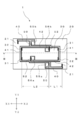
- FIG. 1 is an exploded perspective view showing the micro movable mechanism 1 and the variable capacitance capacitor 2 of the first embodiment
- FIG. 2 is a plan view for explaining the micro movable mechanism 1 and the variable capacitance capacitor 2 of the first embodiment. is there.
- the minute movable mechanism 1 includes a fixed portion 10, a first movable portion 20, a link portion 40 coupled to the first coupling portion 21, and a second coupling portion 31.
- the movable portion 30 and the fulcrum portion 50 are provided.
- the link part 40 is arrange
- the link portion 40 is rotatably provided with the fulcrum portion 50 as a fulcrum, and the fulcrum portion 50 is supported by the joint support portions 15a and 15b to fix the first movable portion 20 and the second movable portion 30. It was arranged at intervals with respect to the part 10.
- the first auxiliary link portion 42 is connected to the third connecting portion 32 of the second movable portion 30.
- the first auxiliary link portion 42 operates in synchronization with the rotation of the link portion 40, and the movable portion 30 is displaced in the Z1-Z2 direction by the operation of the link portion 40 and the first auxiliary link portion 42.
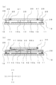
- FIG. 3 is a schematic view for explaining the operation of the first movable portion 20 and the second movable portion 30, and is a cross-sectional view taken along the line III-III in FIG. Fig.3 (a) is a schematic diagram of the initial state to which external force is not given, FIG.3 (b) is a schematic diagram of the state displaced by external force.
- the first movable portion 20 has a first movable electrode 25 on the surface facing the fixed portion 10.
- the second movable portion 30 has a second movable electrode 35 on the surface facing the fixed portion 10.
- the first movable portion 20 is a conductive material, and the material of the first movable portion 20 functions as the first movable electrode 25.
- the second movable portion 30 is a conductive material, and the material of the second movable portion 30 functions as the second movable electrode 35.
- the fixed portion 10 has a first fixed electrode 11 for causing the first movable electrode 25 constituting the variable capacitance capacitor 2 to approach, and between the first movable electrode 25 and the first fixed electrode 11.
- a wire (not shown) for applying a potential difference is connected to the In addition, a wiring having a second fixed electrode 12 opposed to the second movable electrode 35 and for extracting an electric capacity formed between the second movable electrode 35 and the second fixed electrode 12 to the outside. (Not shown) is connected.
- the variable capacitance capacitor 2 has an electric capacity formed between the second movable electrode 35 and the second fixed electrode 12 by the potential difference applied between the first movable electrode 25 and the first fixed electrode 11. Can change.
- the first movable electrode 25 and the first fixed electrode 11 will be referred to as a drive electrode.
- the second movable electrode 35 and the second fixed electrode 12 will be referred to as a capacitive electrode.
- the opposing surface is formed flat so that the capacitive electrode forms a parallel flat plate.
- the opposing surface of the capacitive electrode has a flat area perpendicular to the movable direction Z1-Z2, and is displaced in parallel to the flat area. At any position in the variable range in the Z1-Z2 direction, the capacitive electrode maintains the parallel plate state.
- parallel plate is an expression representing the physical principle of a capacitor, and is not limited to a strictly parallel state.
- the first movable portion 20 and the second movable portion 30 are minute.
- the length of the first movable portion 20 in the X1-X2 direction is 1 mm or less
- the length in the Y1-Y2 direction is 0.1. It is 8 mm or less.
- the thickness dimension is 0.1 mm or less.
- the torsional deformation is an elastic deformation and has a restoring force that tends to return to the torsional deformation.
- FIGS. 1 to 3 show only the portions necessary to explain the present invention
- the fixed portion 10 has a pad electrode portion on the outer peripheral portion for taking out the wiring to the outside, and a minute movable It is practical that it is covered with a protection part for protecting the mechanism 1.
- a control unit for controlling the electric capacity of the variable capacitance capacitor 2 is connected, and a potential difference for generating an electrostatic force in the drive electrode is supplied from the control unit.
- the amount of displacement can be controlled by the balance between the electrostatic force and the restoring force generated in the minute movable mechanism 1.
- the second movable portion 30 is displaced in the direction away from the fixed portion 10 (in the Z1 direction) Do.
- the fulcrum portion 50 is supported by the joint support portion 15 a and acts as a rotation center of the pivotal movement of the link portion 40.
- the amount of displacement of the second movable portion 30 with respect to the amount of displacement of the first movable portion 20 increases in proportion to the ratio of L1 and L2.
- the link portions 40 provided at two places are arranged point-symmetrically.
- the distance between the third connection portion 32 and the fulcrum portion 52 is set to be the same length as the distance (L2) between the second connection portion 31 and the fulcrum portion 50. ing. Thereby, the first auxiliary link unit 42 operates in conjunction with the operation of the link unit 40.
- the distance (L 2) between the second connection portion 31 and the fulcrum portion 50 is longer than the distance (L 1) between the first connection portion 21 and the fulcrum portion 50.
- the position where no potential difference is applied is defined as the position in the initial state, and the amount of displacement due to the pivoting operation about the fulcrum 50 is the amount of displacement of the first movable portion 20 ( ⁇ D1), It is defined as the displacement (.DELTA.D2) of the movable portion 30 of No.2.
- the initial state also includes that no external force such as acceleration is applied.
- the displacement amount ( ⁇ D2) of the second movable portion 30 is larger than the displacement amount ( ⁇ D1) of the first movable portion 20.
- the inter-electrode distance (A2) (of the capacitive electrode) between the portion 30 (second movable electrode 35) and the second fixed electrode 12 largely changes.
- A1 is (.DELTA.D1 + D1').
- A2 is (.DELTA.D2 + D2').
- the capacitance in the initial state is higher than the ratio of the interelectrode distance (A1) in the displaced state to the interelectrode distance (D1 ') in the initial state.
- the ratio of the inter-electrode distance (A2) in the displaced state to the inter-electrode distance (D2 ') of the electrodes can be increased.
- the first movable portion 20 and the second movable portion 30 are respectively connected to the link portion 40 and can be displaced with the fulcrum portion 50 provided on the link portion 40 as a fulcrum.
- the amount of displacement can be freely changed by relatively changing the distance between the point 21 and the second connecting portion 31 with the fulcrum position of the link portion 40.
- the space between the first movable portion 20 and the second movable portion 30 is sufficient for the clearance necessary for the movement, and the dead space may increase when the distance to the fulcrum position is changed. Absent. Since it is not necessary to enlarge the inter electrode distance of the 1st fixed electrode 11 and the 2nd fixed electrode 12 which are provided in fixed part 10 by this, the whole size does not change. Therefore, it is possible to increase the variable ratio without increasing the overall size.
- the electric capacity of the capacitor can be approximated by the formula for the ideal parallel plate electrode when the distance between the electrodes is smaller than the electrode area of the parallel plate electrode. That is, it is proportional to the electrode area and the dielectric constant between the electrodes, and inversely proportional to the distance between the electrodes. Therefore, the capacitance of the variable capacitance capacitor 2 is maximum when the distance between the capacitive electrodes is minimum, and is minimum when the distance between the electrodes is maximum. Also, the variable ratio of the variable capacitance capacitor 2 is equal to the ratio of the minimum to the maximum of the distance between the electrodes.
- the inter-electrode distance is 1 [mu] m ⁇ 2 [mu] m of the capacitor electrode, an electrode area assuming a vacuum dielectric constant of 0.01 mm 2, it becomes capacitance of about 0.9 pF ⁇ 0.45 pF.
- the variable ratio in this case is 2.
- the capacitive electrode and the drive electrode have a simple structure of a parallel plate electrode movable integrally.
- the controllable variable range is about 0.67 ⁇ m for the same inter-electrode capacitance due to the pull-in effect.
- the variable ratio at the electrodes is around 1.3.
- the inter-electrode distance of the drive electrode is expanded to 3 ⁇ m or more in the initial state so as to be within a variable range of 1/3 or less of the inter-electrode distance in the initial state
- the range can be 1 ⁇ m.
- the control voltage required for the electrostatic drive becomes large.
- the distance between the electrodes in the conventional variable capacitance capacitor 102 is 2 ⁇ m
- the distance between the electrodes in the conventional variable capacitance capacitor 102 is 2 ⁇ m
- the distance between the beam 112 and the beam 150 is about twice the distance between the drive electrode 111 and the beam 150.
- the distance between electrodes is 1 ⁇ m
- the distance must be increased by about 3 to 4 times, which is not a practical size.
- the distance between the drive electrodes is 1 ⁇ m in the initial state, and the ratio of L1: L2 to the fulcrum 50 is 1: 3, the distance between the capacitance electrodes is 1 ⁇ m to A variable range of 2 ⁇ m can be made.
- the ratio of L1: L2 is set to 1: 6
- the distance between the capacitive electrodes can be made variable within a range of 1 ⁇ m to 4 ⁇ m, and the variable ratio can be set to 4.
- Such a minute moving mechanism 1 can be manufactured as follows.
- a contact hole portion for electrical connection is formed using a substrate in which SiO 2 is formed between a Si substrate called an SOI (Silicon On Insulator) substrate and a surface Si layer, and then electrical connection and a bonding material are A metal layer was also formed.
- the surface Si layer was processed into a pattern of the first movable portion 20, the second movable portion 30, the link portion 40, the fulcrum portion 50, the bonding portion 55, and the like. Furthermore, the SiO 2 remaining in the pattern other than the bonding portion 55 was removed by etching, and processed so as to be connected by only the bonding portion 55.
- an insulating layer and a metal layer are formed on a Si substrate, the metal layer is processed into a wiring pattern, then SiO 2 is formed, and a contact hole for electrical connection is formed on a part of SiO 2. It formed.
- the wiring was electrically connected by contact holes, and a metal layer was formed so as to protrude from SiO 2 and processed into a desired pattern, thereby forming junction supports 15a, 15b, 16a, 16b which also served as an electrical connection.
- a metal layer was formed into a film and processed into a desired pattern so as to be electrically connected to a wire different from the above by a contact hole, and the first fixed electrode 11 and the second fixed electrode 12 were formed.
- the bonding portion 55 of the SOI substrate and the bonding support portions 15a, 15b, 16a and 16b of the Si substrate were aligned so as to overlap in plan view, and were bonded by metal bonding.
- the inter-electrode distance (D1 ') between the first movable portion 20 (the first movable electrode 25) and the first fixed electrode 11 is determined by the junction of the junction 55 and the junction support 15a, 15b, 16a, 16b. It is set to a desired size. The distance between the electrodes (D1 ') can be increased by increasing the amount of protrusion of the bonding support portions 15a, 15b, 16a, 16b.
- the SiO 2 of the SOI substrate is etched away, the second movable portion 30 can be moved in the direction away from the second fixed electrode 12.
- the SiO 2 thickness (the amount of the gap formed by etching) of the SOI substrate limits the variable range.
- an SOI substrate having a thickness of SiO 2 equal to or larger than the variable range size required for the micro movable mechanism 1 was used.
- a pad electrode portion is provided outside the planar position of the micro movable mechanism 1 in the wiring, and the pad connected to the first movable portion 20 (the first movable electrode 25) and the first fixed electrode 11
- the control unit is electrically connected to the electrode unit.
- the inter-electrode distance (A1) of the drive electrode can be controlled by the electrostatic force due to the potential difference supplied from the control unit.
- the first movable portion 20, the second movable portion 30, and the link portion 40 have rigidity determined by the physical property value of Si, and are provided with a thickness that does not deform with the magnitude of the applied external force.
- the first connecting portion 21, the second connecting portion 31, the fulcrum portion 50 and the like have lengths and widths so as to be able to be torsionally deformed by elastic deformation. This torsional deformation enables displacement by electrostatic force and generates a restoring force to be restored.
- the dimensions of the member to be torsionally deformed are, for example, 30 ⁇ m in length, 1.5 ⁇ m in width, and 1.5 ⁇ m in thickness. Such dimensions were determined so that stress such as torsional deformation was sufficiently small relative to the fracture stress of Si.
- the distance (L1) between the first connecting portion 21 and the fulcrum 50 by changing the arrangement positions of the fulcrums 50, 52 and the joint support 55a, 55b, 56a, 56b in the X1-X2 direction,
- L1 becomes short and L2 becomes long simultaneously. Therefore, the amplification factor in the variable range can be largely changed on the basis of the arrangement in which L1 and L2 are equal.
- the first movable unit 20, the second movable unit 30, the link unit 40, and the like are made of Si and thus have conductivity.
- Si which is a semiconductor material contains dopants, such as B and P, and is low-resistance-ized. Therefore, the first movable portion 20 functions as the first movable electrode 25 without particularly adding an electrode material.
- the second movable portion 30 functions as a second movable electrode 35.
- a metal layer having a lower resistance may be stacked.
- the thermal expansion coefficient of the substrate is the same, and the thermal stress is small. Therefore, even if the environmental temperature changes, the variation of the displacement amount is small.
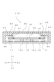
- FIG. 4 is a cross-sectional view for explaining the micro movable mechanism 1 and the variable capacitance capacitor 2 of the second embodiment.
- FIG. 4A is a schematic view of an initial state in which no external force is applied
- FIG. 4B is a schematic view of a state in which the external force is displaced.
- the same components as those in the first embodiment are denoted by the same reference numerals.
- the second embodiment is different from the first embodiment in that the first fixed electrode 11 is provided with a stopper 18 and the first movable portion 20 is provided with a stopper 28.
- the variable range of the first movable portion 20 is limited to the position where the stopper 18 and the stopper 28 contact with each other.
- the stopper 18 and the stopper 28 may be provided only in one of them.
- the displacement amount ( ⁇ D1) of the first movable portion 20 is 3 of the inter-electrode distance (D1 ′) between the first movable portion 20 (first movable electrode 25) and the first fixed electrode 11 in the initial state. It is preferable that the stopper 18 and the stopper 28 be provided at a height at which the stopper 18 and the stopper 28 contact with each other so as to be limited to one-half or less. If ⁇ D1 is one-third or more of D1 ′, the pull-in effect in which the electrostatic force exceeds the restoring force can not return to the initial state only by the restoring force. By providing the heights of the stopper 18 and the stopper 28 so as to be limited to one third or less of D1 ', the pull-in effect can be prevented.
- the stopper is a first movable portion 20, a fixed portion 10 facing the first movable portion 20, a first fixed electrode 11, an Si substrate (not shown) of an SOI substrate facing the second movable portion 30,
- the second movable portion 30 can be provided on the surface facing the Si substrate (not shown) of the SOI substrate.
- the stopper may be provided at one position of any one of the above members, but may be divided into a plurality of members as shown in FIG. 4 (a). Also, as shown in FIG. 4A, stoppers may be provided at a plurality of places.
- the material of the stopper may be selected to be sufficiently resistant to contact during operation. Further, in the case where the contact of the electrodes is not electrically preferable, an insulating material may be used. More preferably, the electrode may be disposed at a position avoided.
- another stop may be provided to limit the displacement in the reverse direction.
- another stopper is provided on either the second movable portion 30 or the second fixed electrode 12, it is possible to limit the displacement in the reverse direction from the initial state of FIG. 4A.
- the micro movable mechanism 1 is configured so that displacement in the reverse direction can also be limited, in addition to the control method of controlling the displacement amount by balancing the electrostatic force and the restoring force, the stopper stably stabilizes the displacement amount at the limited position. It is possible to gain control. For example, it is most suitable for the use which uses variable capacity capacitor 2 by two values of the minimum value of electric capacity, and the maximum value. Since the displacement amount is fixed by the stopper, the electric capacity is stabilized, and error factors such as time fluctuation of the control voltage can be reduced. Also for the stopper that limits the displacement in the reverse direction, the installation location can be selected without departing from technical common sense.
- FIG. 5 is an exploded perspective view showing the micro movable mechanism 1 and the variable capacitance capacitor 2 of the third embodiment.
- the joint support portions 15a, 15b, 16a, 16b are disposed substantially at the center in the X1-X2 direction, and are different from the first embodiment, but the first connecting portion 21 is different from the first embodiment. Position is closer to the center in the X1-X2 direction than in FIG.
- a second auxiliary link 43 is provided.
- the distance between the fourth connecting portion 23 and the fulcrum portion 53 is set such that the second auxiliary link portion 43 has the same length as the distance (L1) between the first connecting portion 21 and the fulcrum portion 50. ing.
- the distance (L2) between the second connection portion 31 and the fulcrum portion 50 is longer than the distance (L1) between the first connection portion 21 and the fulcrum portion 50.
- the position of the fulcrum portion 50 is substantially fixed, and the distance (L2) between the second connecting portion 31 and the fulcrum portion 50 is constant, and the first connecting portion 21 and the fulcrum The amount of displacement ( ⁇ D2) of the second movable portion 30 was adjusted according to the distance (L1) to the portion 50.
- the SOI substrate including the link portion 40 in addition to the pattern shown in FIG. 5, it is possible to manufacture a pattern in which the total length of the link portion 40 is changed to change the ratio of L1 and L2.
- the fixed portion 10 may be a substrate of the same design, so it becomes easy to manufacture a plurality of types of variable capacitance capacitors 2.
- junction support portions 15a, 15b, 16a and 16b are disposed substantially at the center in the X1-X2 direction, the variable capacitance capacitor 2 having an almost shock-resistant configuration is obtained.
- a second auxiliary link 43 is provided.
- the second auxiliary link portion 43 it is possible to prevent the first movable portion 20 from tilting and operating. Since the inclination of the first movable portion 20 can be prevented, the first fixed electrode 11 provided in the fixed portion 10 may be only in one of the X1-X2 directions.
- the stoppers 18 and 28 may be provided.
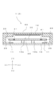
- FIG. 6 is a cross-sectional view for explaining a micro movable mechanism 1 and a variable capacitance capacitor 2 according to a fourth embodiment.
- FIG. 6 (a) is a schematic view of an initial state in which no external force is applied
- FIG. 6 (b) is a schematic view of a state in which the external force is displaced.
- the same components as those in the first embodiment are denoted by the same reference numerals.
- the fourth embodiment is such that the distance from the first movable portion 20 to the first fixed electrode 11 is not on the same plane as the second fixed electrode 12 with respect to the first embodiment. It differs in being provided.
- the second fixed electrode 12 is disposed so as to project toward the second movable portion 30 more than the first fixed electrode 11.
- the inter-electrode distance (D1 ') of the drive electrode in the initial state and the inter-electrode distance (D2') of the capacitive electrode in the initial state are D1 '> D2'.
- the ratio of the inter-electrode distance (A2) of the capacitive electrode in the displaced state to the D2 ′ can be further increased compared to the ratio of the inter-electrode distance (A1) of the drive electrode in the displaced state to the D1 ′. it can.
- Such a fixed portion 10 can be easily manufactured if the film thickness of the SiO 2 film is made different before forming the first fixed electrode 11 and the second fixed electrode 12 in the manufacturing process. be able to. Further, in order to increase the inter-electrode distance of the drive electrodes, the surface of the first movable portion 20 facing the first fixed electrode 11 (the electrode surface of the first movable electrode 25) and the second movable portion 30. The surface facing the second fixed electrode 12 (the electrode surface of the second movable electrode 35) may not be on the same plane, but may be different.
- the distance between the first movable portion 20 (the first movable electrode 25) in the initial state and the first fixed electrode 11 is 1 ⁇ m
- the second movable portion 30 in the initial state (the second movable electrode (the second movable electrode) 35) and the second fixed electrode 12 is 0.25 ⁇ m
- the ratio of L1: L2 to the fulcrum 50 is 1: 3
- the distance between capacitive electrodes is 0.25 ⁇ m to A variable range of 1.25 ⁇ m can be made.
- variable ratio of the variable capacitance capacitor 2 can be set to five. Furthermore, when the inter-electrode distance of the capacitive electrode is narrowed, the variable capacitance capacitor 2 having a large electrical capacitance can be obtained because the value of the electrical capacitance at the same electrode area is large. Moreover, if it is the variable capacitor 2 of the same electric capacity, it is possible to miniaturize.
- the ratio of D1 ': D2' and the ratio of L1: L2 can be varied independently, and the variable ratio can be synergistically increased. Therefore, the variable capacitance capacitor 2 having a large variable ratio can be realized as compared with the conventional case.
- the present embodiment can be combined with the configuration in which the stoppers 18 and 28 described in the second embodiment are provided and the configuration in which the second auxiliary link portion 43 described in the third embodiment is provided.
- FIG. 7 is a cross-sectional view for explaining the micro movable mechanism 1 and the variable capacitance capacitor 2 of the fifth embodiment, and is a schematic view of an initial state.
- the protective portion 60 omitted in FIGS. 1 to 5 is schematically shown.
- the protective portion 60 is provided with a third fixed electrode 61 facing the first movable portion 20.
- the other configuration is the same as that of the first embodiment, and the same components as those of the first embodiment are denoted by the same reference numerals.
- the member corresponded in the joint support parts 15b and 16b in the protection part 60 is not shown in figure.
- the first movable portion 20 functions as a third movable electrode 26 opposed to the third fixed electrode 61.
- the electrostatic force can be driven in the approaching direction. Therefore, the electrostatic force is intended to be displaced in the opposite direction to the electrostatic force due to the potential difference between the first movable portion 20 (the first movable electrode 25) and the first fixed electrode 11, and only by the restoring force. It is possible to stabilize the balance of displacement rather than balancing. Further, the speed of switching the electric capacity of the variable capacity capacitor 2 to an arbitrary set value can be increased.
- FIG. 8 is a cross-sectional view for explaining the micro movable mechanism 1 and the variable capacitance capacitor 2 of the sixth embodiment, and is a schematic view of an initial state. Similar to FIG. 7, FIG. 8 schematically shows the protective portion 60 which is omitted in FIGS.
- the second fixed electrode 12 is provided on the surface of the protection unit 60 facing the second movable unit 30. Similar to the first embodiment, the opposing surface is formed flat so that the second movable electrode 35 and the second fixed electrode 12 form a parallel flat plate. As in the first embodiment, the first movable portion 20 (first movable electrode) is generated by the electrostatic force due to the potential difference between the first movable portion 20 (the first movable electrode 25) and the first fixed electrode 11. When the distance between the electrodes 25) and the first fixed electrode 11 approaches, the distance between the second movable portion 30 and the fixed portion 10 operates to be separated.
- the second movable portion 30 of the present embodiment since the surface different from the surface facing the fixed portion 10 constitutes the second movable electrode surface 35 and the electric capacitance with the second fixed electrode 12, The inter-electrode distance between the second movable electrode surface 35 and the second fixed electrode 12 operates in the approaching direction.
- variable capacitance capacitor 2 Since, also in this case, it functions as the variable capacitance capacitor 2.
- FIG. 9 is an exploded perspective view showing the micro movable mechanism 1 and the variable capacitance capacitor 2 of the seventh embodiment.
- the same components as those in the first embodiment are denoted by the same reference numerals.
- the seventh embodiment is different from the first embodiment in that the second fixed electrode 12 is provided by being divided into two divided electrodes 12 a and 12 b.
- Each of the divided electrodes 12a and 12b constitutes a capacitive electrode with the second movable portion 30 (second movable electrode 35), and is connected to a wire (not shown).
- the second movable portion 30 serves as an intermediate electrode, and a variable capacitance capacitor in which two capacitors are connected in series It can function as 2.
- the capacitance of the series connection is reduced to about half, the resistance of the wiring can be reduced, so that the parasitic resistance of the variable capacitance capacitor 2 can be reduced.
- the parasitic inductance of the variable capacitance capacitor 2 can be reduced. Therefore, the variable capacitance capacitor 2 suitable for high frequency circuit applications can be realized.
- FIG. 10 is a cross-sectional view for explaining the micro movable mechanism 1 and the mirror device 3 of the eighth embodiment.
- FIG. 10A is a schematic view of an initial state in which no external force is applied
- FIG. 10B is a schematic view of a state in which the external force is displaced.
- the same components as those in the first embodiment are denoted by the same reference numerals.
- the eighth embodiment differs from the first embodiment in that the second fixed electrode 12 is not provided. Furthermore, the second movable portion 30 has a mirror surface 30 a, and the mirror surface 30 a is provided on a surface different from the surface facing the fixed portion 10.
- the mirror surface 30a can be applied to an apparatus that applies the mirror surface 30a optically.
- the mirror surface 30a is formed to be a plane mirror and used as a light reflection surface, the mirror device 3 having a large variable range can be configured.
- the variable direction is the Z1-Z2 direction, and the inclination of the mirror surface 30a can be suppressed. Therefore, the present invention can be applied to an optical device that variably controls the optical path length in the Z1-Z2 direction.
- the present invention is not limited to the first to eighth embodiments, and various modifications can be made as needed.
- variable capacitance capacitor 2 if the larger movable distance is used as the capacitance electrode, the variable ratio can be increased as described above.
- the functions of the first movable portion 20 (first movable electrode 25) and the second movable portion 30 (second movable electrode 35) can be switched.
- the movable distance of the capacitive electrode is reduced, precise control is possible within the movable range. Therefore, it is suitable for the use method which controls precise electric capacity, even if the variable range is small.
- the functions of the first movable portion 20 and the second movable portion 30 can be interchanged.
- an electrostatic force is generated between the first movable portion 20 (the first movable electrode 25) and the first fixed electrode 11 by application of the drive voltage, and the distance between the drive electrodes is determined by the electrostatic force.
- the electrostatic force may be generated in an electrode shape called a comb electrode.
Abstract
【課題】大きな可変範囲を有する微小可動機構及び可変容量コンデンサを提供することを目的としている。 【解決手段】本発明の微小可動機構1は、固定部10に対して間隔を設けて配置された第1の可動部20と、第1の連結部21に連結されたリンク部40と、第2の連結部31を備える第2の可動部30と、支点部50と、を有し、リンク部40は支点部50を支点として回動可能に設けられ、第1の連結部21と支点部50との距離よりも、第2の連結部31と支点部50との距離が長くなる位置に設けられた、ことを特徴とする。
Description
本発明は、微小可動機構及び可変容量コンデンサに関し、特に、大きな可変範囲を有する微小可動機構及び可変容量コンデンサに関する。
微小可動機構を用いた可変容量コンデンサは、携帯電話に搭載する回路部品の点数を削減して小型化に寄与することが期待されて、開発が進められている。
このような可変容量コンデンサは、MEMS(Micro Electro Mechanical Systems)と呼ばれる微小デバイス技術によって大量生産することが可能である。MEMSは小型化に適していて、大量生産すれば比較的安価な製品にすることができるので、携帯機器の小型化や高性能化に寄与することが期待される。さらに、携帯電話に使用されている周波数帯域は700MHz~2.5GHz等の広い帯域であるため、最小の電気容量に対して最大の電気容量が10倍程度の可変比を有する可変容量コンデンサが要望されている。
たとえば、特許文献1に開示されているように、支持部と、支持部から延在して設けられた梁で中央部が保持された可動部と、を有する微小可動機構を利用し、支持部に設けられた固定電極と、固定電極に対向する可動部と、によって、可変容量コンデンサの電極が構成された。可動部の変位によって電極間距離が変わるので、可変容量コンデンサの電気容量を可変にできる。
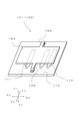
図11に示すように、従来の可変容量コンデンサ102には、従来の微小可動機構101が利用された。従来の微小可動機構101は、可動部120の中央部の2箇所に梁150が固定されて、可動部120は梁150のねじれによって回転可能になっている。支持部110(固定部)には、固定電極として駆動電極111と検出電極112とが、可動部120に対向して設けられている。
この微小可動機構101において、駆動電極111(第1の固定電極)に電圧を印加すると、電圧が印加された駆動電極111と、可動部120と、の間に電位差が発生して、静電力(クーロン力)を生じる。この静電力によって可動部120が梁150を回転軸として回転するので、電気容量を検出する検出電極112(第2の固定電極)と可動部120との対向する部分の電極間距離が変化する。
このとき、静電力と、梁150のねじれに対する材料力学的な復元力と、が均衡した位置まで変位して、検出電極112と可動部120との電気容量が変化する。駆動電極111に印加する電圧値によって、復元力と均衡している変位位置を変化させて、所望の電気容量に調整することができる。ただし、可動部120と駆動電極111との可変範囲を静電力の無い状態の3分の1以上に大きく変化させようとすると、静電力と復元力との均衡を保つことができない。これはプルイン効果と呼ばれる現象で、静電駆動方式における制御可能な可変範囲に制限を与えている。
このような可変容量コンデンサ102の可変比は、検出電極112と可動部120との実効電極間距離の、制御可能な可変範囲における最小値と最大値との比率以内に制限される。ここで、図11の可動部120は梁150を回転軸として傾くので、平行平板に近似したときの電極間距離を実効電極間距離と定義した。可変比を大きくするためには、可動部120と検出電極112との実効電極間距離の可変範囲を大きくしなければならない。
ここで、可動部120と駆動電極111との間に電位差が印加されていない位置を初期状態と定義する。可変範囲を大きくする方法として、初期状態において可動部120と駆動電極111との実効電極間距離を大きくすると、必要な静電力を発生させるための駆動電圧が大きくなってしまう。そこで、図11に示すように、駆動電極111の位置と比較して、検出電極112を梁150からX2方向に離して配置しなければならなかった。しかしながら、大きな可変範囲を得るためには、検出電極112と梁150との配置を離さなければならないので、全体の寸法が大きくなってしまう。
このように、従来の微小可動機構では、可変範囲を大きくすることが実用上困難であった。そのため、大きな可変範囲を有する可変容量コンデンサは実現されていなかった。
本発明は上記課題を解決するためのものであり、特に、大きな可変範囲を有する微小可動機構及び可変容量コンデンサを提供することを目的とする。
本発明の微小可動機構は、固定部に対して間隔を設けて配置された第1の可動部と、前記第1の可動部に設けられた第1の連結部に連結されたリンク部と、前記リンク部に連結された第2の連結部を備える第2の可動部と、前記第1の連結部と前記第2の連結部の間に位置し、前記リンク部に設けられた支点部と、を有し、前記リンク部は、前記第1の可動部が前記固定部に接近するとき前記第2の可動部が前記固定部から離れるように、前記支点部を支点として回動可能に設けられ、前記支点部は、前記第1の連結部と前記支点部との距離よりも、前記第2の連結部と前記支点部との距離が長くなる位置に設けられた、ことを特徴とする。
こうすれば、第1の可動部と第2の可動部とはリンク部にそれぞれ連結されて、リンク部に設けた支点部を支点とした変位が可能になるので、第1の連結部とリンク部の支点位置との距離に対して、第2の連結部とリンク部の支点位置との距離を、相対的に変えることによって、変位量を大きくすることができる。第1の可動部に設けられた第1の連結部と支点部との距離(L1)よりも、第2の可動部に設けられた第2の連結部と支点部との距離(L2)が長いので、支点部を支点とした回動動作による変位量は、第1の可動部の変位量(ΔD1)よりも第2の可動部の変位量(ΔD2)が大きい。すなわち、初期状態での第2の可動部と固定部との間隔(D2)から、最大位置(ΔD2+D2)までを可変範囲とすることができる。
したがって、本発明の微小可動機構は、大きな可変範囲を有する。
さらに、前記第2の可動部は、可動方向に垂直な平面領域を有していることが好適である。可動方向に垂直な平面領域が傾くことなく平行に変位するので、平面領域を平面鏡や平板電極として種々のデバイスに応用可能である。これにより、平面領域を光の反射面として利用すれば、大きな可変範囲を有するミラー・デバイスを構成することができる。また、平面領域を電極面として可変容量コンデンサに用いることができる。
本発明の可変容量コンデンサは、前記第2の可動部が可動方向に垂直な平面領域を有して、前記平面領域に平行に変位する微小可動機構を備えるとともに、前記第1の可動部は第1の可動電極を有し、前記第2の可動部は第2の可動電極を有し、前記固定部は前記第1の可動電極に対向する第1の固定電極を有するとともに、前記第2の可動電極に対向する第2の固定電極を有し、前記第1の可動電極と前記第1の固定電極との間に電位差が印加されていない初期状態を基準にして、前記第1の可動電極と前記第1の固定電極との間に印加された電位差によって、前記第1の可動電極が前記第1の固定電極に接近し、前記第2の可動電極と前記第2の固定電極との間に形成された電気容量を変化させる、ことを特徴とする。
こうすれば、可動状態における第1の可動電極と第1の固定電極との電極間距離(A1)に対して、可動状態における第2の可動電極と第2の固定電極との電極間距離(A2)が大きく変化する。ここで、電位差が印加されていない位置を初期状態の位置と定義して、初期状態での第1の可動電極と第1の固定電極との電極間距離(D1’)を用いると、A1の最大は(ΔD1+D1’)である。なお、初期状態は、加速度等の外力を与えていない状態であることも含んでいる。同様に、初期状態での第2の可動電極と第2の固定電極との電極間距離(D2’)を用いて、A2の最大は(ΔD2+D2’)である。ΔD1よりΔD2が大きいので、A1よりA2を大きくできる。
したがって、本発明の可変容量コンデンサは、大きな可変範囲を有する。
前記初期状態において、前記第1の可動電極と前記第1の固定電極との電極間距離に比べて、前記第2の可動電極と前記第2の固定電極との電極間距離が狭められて配置されたことが好ましい。すなわち、D1’>D2’となるように配置された。こうすれば、初期状態での第2の可動電極と第2の固定電極との電極間距離(D2’)に対して、可動状態における第2の可動電極と第2の固定電極との電極間距離(A2)の最大値の相対比率を大きくすることができる。したがって、制御可能な可変範囲に対して、大きな可変比の可変容量コンデンサを実現できる。
前記固定部において、前記第1の固定電極よりも前記第2の固定電極が突出するように配置されたことが実際的である。このような態様は容易に製作することができる。したがって、制御可能な可変範囲に対して、大きな可変比の可変容量コンデンサを容易に実現できる。
前記微小可動機構はストッパを有し、前記ストッパによって、前記第1の可動電極が前記第1の固定電極に接近できる可動距離が、前記初期状態における前記第1の可動電極と前記第1の固定電極との電極間距離の3分の1以下に制限されていることが好適である。この値が3分の1以上であると、静電力が復元力を上回るプルイン効果によって、復元力だけで初期状態に戻ることができなくなる。該ストッパは、第1の可動部、第1の可動部と対向する固定部、第1の可動電極、第1の固定電極、第2の可動部、第2の可動部と対向する固定部、第2の可動電極、第2の固定電極、に設けることができる。前記いずれかの部材の1箇所に該ストッパを設けていればよいが、複数の部材に分割して設けることもできる。また、複数箇所に設けてもよい。ストッパによって、第1の可動部の変位量(ΔD1)が初期状態での第1の可動電極と第1の固定電極との電極間距離(D1’)の3分の1以下に制限されるので、プルイン効果を防止できる。
本発明によれば、第1の可動部と固定部との間隔の変位量に対して、第2の可動部と固定部との間隔の変位量が大きいので、大きな可変範囲を有する微小可動機構を実現できる。
以下、本発明の実施の形態について図面を用いて詳細に説明する。なお、分かりやすいように、図面の寸法を適宜変更している。
<第1の実施形態>
図1は第1の実施形態の微小可動機構1及び可変容量コンデンサ2を示す分解斜視図であり、図2は第1の実施形態の微小可動機構1及び可変容量コンデンサ2を説明する平面図である。
図1は第1の実施形態の微小可動機構1及び可変容量コンデンサ2を示す分解斜視図であり、図2は第1の実施形態の微小可動機構1及び可変容量コンデンサ2を説明する平面図である。
図1に示すように、微小可動機構1は、固定部10と、第1の可動部20と、第1の連結部21に連結されたリンク部40と、第2の連結部31を備える第2の可動部30と、支点部50と、を有している。図1ではリンク部40が2箇所に配置されている。リンク部40は支点部50を支点として回動可能に設けられ、支点部50は接合支持部15a、15bに支持されることによって、第1の可動部20と第2の可動部30とが固定部10に対して間隔を設けて配置された。また、第1の補助リンク部42が第2の可動部30の第3の連結部32に連結されている。第1の補助リンク部42はリンク部40の回動に同期して動作し、リンク部40と第1の補助リンク部42との動作によって、可動部30はZ1-Z2方向に変位する。
図3は第1の可動部20及び第2の可動部30の動作を説明する模式図であって、図2のIII-III線に沿って切断した断面図である。図3(a)は外力が与えられていない初期状態の模式図であり、図3(b)は外力により変位した状態の模式図である。
図3(a)に示すように、第1の可動部20は、固定部10と対向する面に第1の可動電極25を有している。第2の可動部30は、固定部10と対向する面に第2の可動電極35を有している。なお、第1の可動部20は導電性材料であり、第1の可動部20の材料が第1の可動電極25として機能している。同様に、第2の可動部30は導電性材料であり、第2の可動部30の材料が第2の可動電極35として機能している。固定部10には、可変容量コンデンサ2を構成する第1の可動電極25を接近させるための第1の固定電極11を有し、第1の可動電極25と第1の固定電極11との間に電位差を印加するための配線(図示していない)が接続されている。また、第2の可動電極35に対向する第2の固定電極12を有し、第2の可動電極35と第2の固定電極12との間に形成された電気容量を外部に取り出すための配線(図示していない)が接続されている。可変容量コンデンサ2は、第1の可動電極25と第1の固定電極11との間に印加した電位差によって、第2の可動電極35と第2の固定電極12との間に形成された電気容量を変化させることができる。以下の説明では、第1の可動電極25と第1の固定電極11とを、駆動電極と呼ぶことにする。また、第2の可動電極35と第2の固定電極12とを、容量電極と呼ぶことにする。
このとき、容量電極が平行平板を形成するように対向面が平面に形成されている。容量電極の対向面は、可動方向であるZ1-Z2方向に垂直な平面領域を有し、平面領域に平行に変位する。Z1-Z2方向の可変範囲のいずれの位置においても、容量電極は平行平板の状態を維持している。なお、ここで言う「平行平板」とはコンデンサの物理的原理を表わす表現であり、厳密な平行状態に限定されない。
第1の可動部20及び第2の可動部30は微小であり、たとえば、第1の可動部20のX1-X2方向の長さは1mm以下であり、Y1-Y2方向の長さは0.8mm以下である。さらに、厚み寸法は0.1mm以下である。
第1の可動部20と第2の可動部30とが変位したとき、第1の連結部21、第2の連結部31、第3の連結部32、及び支点部50、52は、ねじれ変形する。このねじれ変形は弾性変形であって、ねじれ変形に対して元に戻ろうとする復元力を有している。
なお、図1~図3では、本発明を説明するために必要な部分のみを示しているが、固定部10は外周部に配線を外部に取り出すためのパッド電極部を有し、また微小可動機構1を保護するための保護部で覆われていることが実用的である。さらに、可変容量コンデンサ2の電気容量を制御する制御部が接続されて、駆動電極に静電力を発生させるための電位差が制御部から供給される。
こうすれば、微小可動機構1に生じる静電力と復元力との均衡によって変位量を制御することができる。図1に示すように、第1の可動部20が固定部10に近づく方向に(Z2方向に)変位したとき、第2の可動部30は固定部10から離れる方向に(Z1方向に)変位する。図2に示すように、第1の連結部21と支点部50との距離(L1)よりも、第2の連結部31と支点部50との距離(L2)が長くなる位置に、支点部50を設けている。支点部50は接合支持部15aに支持されて、リンク部40の回動動作の回転中心として作用する。したがって、L1とL2との比率に比例して、第1の可動部20の変位量に対する第2の可動部30の変位量が大きくなる。図2から分かるように、2箇所に設けられたリンク部40は点対称に配置されている。
第1の補助リンク部42は、第2の連結部31と支点部50との距離(L2)と同じ長さになるように、第3の連結部32と支点部52との距離が設定されている。これにより、リンク部40の動作に連動して、第1の補助リンク部42は動作する。
図3(a)、(b)を参照して、第1の可動部20及び第2の可動部30の動作について説明する。
図2に示すように、第1の連結部21と支点部50との距離(L1)よりも第2の連結部31と支点部50との距離(L2)が長い。ここで、電位差が印加されていない位置を初期状態の位置と定義して、支点部50を支点とした回動動作による変位量を、第1の可動部20の変位量(ΔD1)と、第2の可動部30の変位量(ΔD2)と定義する。なお、初期状態は、加速度等の外力を与えていない状態であることも含んでいる。この場合、第1の可動部20の変位量(ΔD1)に対して第2の可動部30の変位量(ΔD2)のほうが大きい。このため、回動動作時に、第1の可動部20(第1の可動電極25)と第1の固定電極11との(駆動電極の)電極間距離(A1)に対して、第2の可動部30(第2の可動電極35)と第2の固定電極12との(容量電極の)電極間距離(A2)が大きく変化する。初期状態での駆動電極の電極間距離(D1’)を用いると、A1は(ΔD1+D1’)である。同様に、初期状態での容量電極の電極間距離(D2’)を用いると、A2は(ΔD2+D2’)である。図3(a)、(b)に示すように、初期状態での駆動電極の電極間距離(D1’)に対する変位状態での電極間距離(A1)の比率に比べて、初期状態での容量電極の電極間距離(D2’)に対する変位状態での電極間距離(A2)の比率を大きくすることができる。
第1の可動部20と第2の可動部30とはリンク部40にそれぞれ連結されて、リンク部40に設けられた支点部50を支点とした変位が可能になるので、第1の連結部21と第2の連結部31とでリンク部40の支点位置との距離を相対的に変えることによって、変位量を自在に変えることができる。このとき、第1の可動部20と第2の可動部30と間のスペースは可動に必要なクリアランス程度で十分であり、支点位置との距離を変えるときにデッドスペースが増加してしまうこともない。これにより、固定部10に設ける第1の固定電極11と第2の固定電極12との電極間距離を大きくする必要がないので、全体の寸法は変わらない。したがって、全体の寸法を大きくしなくても、可変比を大きくすることが可能になる。
コンデンサの電気容量は、平行平板電極の電極面積に比較して電極間距離が小さいときは、理想の平行平板電極での計算式で近似できる。すなわち、電極面積と電極間の誘電率とに比例し、電極間距離に反比例する。したがって、可変容量コンデンサ2の電気容量は容量電極の電極間距離が最小のときに最大であり、電極間距離が最大のときに最小である。また、可変容量コンデンサ2の可変比は電極間距離の最小と最大との比率に等しい。
たとえば、容量電極の電極間距離が1μm~2μmの可変範囲で、電極面積が0.01mm2の真空誘電率を仮定すれば、約0.9pF~0.45pFの電気容量になる。また、この場合の可変比は2である。
比較例として、容量電極と駆動電極とが、一体に可動する平行平板電極の単純構造を仮定する。初期状態の駆動電極の電極間距離2μmで、電極間距離が狭まる方向に動作させようとする場合、プルイン効果のために、制御可能な可変範囲は約0.67μmで、同じ電極間距離の容量電極での可変比は1.3程度である。そこで、プルイン効果を防止するため、初期状態の電極間距離の1/3以下の可変範囲になるように、駆動電極の電極間距離を初期状態で3μm以上に拡げて配置しておけば、可変範囲を1μmとすることができる。しかし、初期状態の電極間距離3μmに対する静電力を発生させるために必要な電位差を印加しなければならないので、静電駆動に必要な制御電圧が大きくなってしまう。一方、従来の可変容量コンデンサ102で電極間距離を2μmと仮定すれば、駆動電極111の電極面積範囲でプルイン効果を防止して、検出電極112の可変範囲を1μmとするためには、検出電極112と梁150の距離を、駆動電極111と梁150の距離の2倍程度になるように配置しなければならない。さらに、電極間距離を1μmと仮定すれば、その距離を3~4倍程度に延ばさなければならず、実用的な大きさではない。
本実施形態によれば、初期状態で駆動電極の電極間距離を1μmとして、支点部50に対するL1:L2の比率を1:3になるように配置すれば、容量電極の電極間距離を1μm~2μmの可変範囲にできる。また、L1:L2の比率を1:6になるように配置するならば、容量電極の電極間距離を1μm~4μmの可変範囲にでき、可変比を4にできる。これらの可変容量コンデンサ2では、初期状態の駆動電極の電極間距離1μmに対する静電力を印加すればよいので、静電駆動に必要な制御電圧が、比較例に比べて低くできる。
このような微小可動機構1は以下のように製造することができる。
SOI(Silicon On Insulator)基板と呼ばれるSi基板と表面Si層との間にSiO2が形成されている基板を用い、電気接続用のコンタクトホール部を形成してから、電気接続と接合材とを兼ねる金属層を形成した。金属層を所望のパターンに加工してから、第1の可動部20、第2の可動部30、リンク部40、支点部50、接合部55、等のパターンに表面Si層を加工した。さらに、接合部55以外のパターンに残っているSiO2をエッチング除去して、接合部55だけで繋がっている状態に加工した。
これとは別に、Si基板に絶縁層と金属層を成膜して金属層を配線パターンに加工してから、SiO2を成膜して、SiO2の一部に電気接続用のコンタクトホールを形成した。配線にコンタクトホールで電気接続するとともに、SiO2から突出するように金属層を成膜して所望のパターンに加工し、電気接続を兼ねた接合支持部15a、15b、16a、16bを形成した。また、これとは別の配線にコンタクトホールで電気接続するように、金属層を成膜して所望のパターンに加工し、第1の固定電極11と第2の固定電極12とを形成した。
つぎに、SOI基板の接合部55とSi基板の接合支持部15a、15b、16a、16bとを平面視で重なるように位置合わせして、金属接合によって貼り合わせた。
第1の可動部20(第1の可動電極25)と第1の固定電極11との電極間距離(D1’)は、接合部55と接合支持部15a、15b、16a、16bとの接合によって所望の大きさに設定される。接合支持部15a、15b、16a、16bの突出量を大きくすれば、電極間距離(D1’)を大きくすることができる。
また、SOI基板のSiO2がエッチング除去されたので、第2の可動部30は第2の固定電極12から離れる方向に可動できる。この場合は、SOI基板のSiO2の厚さ(エッチングにより形成されたギャップの量)が可変範囲を制限する。あらかじめ、微小可動機構1に必要な可変範囲の大きさ以上のSiO2の厚さを有するSOI基板が使用された。なお、SOI基板からSiO2をエッチング除去する場合、第1の可動部10や第2の可動部20等の平面領域は微細な孔を設けておくことが好ましい。こうすれば、SiO2のエッチング均一性が向上する。微細な孔であれば、可変容量コンデンサとしての電気容量にほとんど影響しない。 なお、SOI基板を使用せず、他の製造方法によって製造することも可能である。
なお、配線には微小可動機構1の平面位置の外側でパッド電極部が設けられ、第1の可動部20(第1の可動電極25)と第1の固定電極11とに接続されているパッド電極部に制御部が電気接続される。こうすれば、駆動電極の電極間距離(A1)は、制御部から供給された電位差による静電力で制御できる。
第1の可動部20、第2の可動部30、及びリンク部40はSiの物性値で定まる剛性を有し、印加される外力の大きさでは変形しない厚さに設けられている。一方、第1の連結部21、第2の連結部31、及び支点部50等は、弾性変形によって、ねじれ変形できるように長さと幅とが形成されている。このねじれ変形によって、静電力での変位を可能とするとともに、元に戻ろうとする復元力が発生する。ねじれ変形する上記部材の寸法は、たとえば、長さ30μm、幅1.5μm、厚さ1.5μmである。このような寸法は、Siの破壊応力に対して、ねじれ変形等の応力が十分に小さくなるように決定された。
なお、支点部50、52と接合支持部55a、55b、56a、56bとの配置位置をX1-X2方向で変えることによって、第1の連結部21と支点部50との距離(L1)と、第2の連結部31と支点部50との距離(L2)とを、変化させる場合、L1が短くなると同時にL2が長くなる。したがって、L1とL2とが等しい配置を基準にして、可変範囲の増幅率を大きく変化させることができる。
第1の可動部20、第2の可動部30、及びリンク部40等は、Siからなるので導電性を有する。なお、半導体材料であるSiは、BやP等のドーパントを含み、低抵抗化されている。したがって、とくに電極材料を付加することなく、第1の可動部20は第1の可動電極25として機能する。同様に、第2の可動部30は第2の可動電極35として機能する。第1の可動部20、第2の可動部30、リンク部40等をさらに低抵抗化させたいときは、より低抵抗の金属層を積層すればよい。
上述のように、SOI基板とSi基板とを接合した微小可動機構1の場合は、基板の熱膨張係数が同じであり、熱応力が小さい。したがって、環境温度が変化しても、変位量の変動が少ない。
<第2の実施形態>
図4は第2の実施形態の微小可動機構1及び可変容量コンデンサ2を説明する断面図である。図4(a)は外力が与えられていない初期状態の模式図であり、図4(b)は外力により変位した状態の模式図である。なお、第1の実施形態と同じものは同じ符号にしている。
図4は第2の実施形態の微小可動機構1及び可変容量コンデンサ2を説明する断面図である。図4(a)は外力が与えられていない初期状態の模式図であり、図4(b)は外力により変位した状態の模式図である。なお、第1の実施形態と同じものは同じ符号にしている。
第2の実施形態は、第1の実施形態に対して、第1の固定電極11にストッパ18が設けられ、第1の可動部20にストッパ28が設けられていることが異なる。図4(b)に示すように、第1の可動部20はストッパ18とストッパ28とが接触する位置に可変範囲が制限される。なお、可変範囲を同じにできれば、ストッパ18とストッパ28は、いずれか一方にのみ設けてもよい。
第1の可動部20の変位量(ΔD1)が、初期状態での第1の可動部20(第1の可動電極25)と第1の固定電極11との電極間距離(D1’)の3分の1以下に制限されるように、ストッパ18とストッパ28とが接触する高さに設けられていることが好ましい。ΔD1がD1’の3分の1以上であると、静電力が復元力を上回るプルイン効果によって、復元力だけで初期状態に戻ることができなくなる。D1’の3分の1以下に制限されるように、ストッパ18とストッパ28との高さを設けることによって、プルイン効果を防止することができる。
ストッパは、第1の可動部20、第1の可動部20と対向する固定部10、第1の固定電極11、第2の可動部30と対向するSOI基板のSi基板(図示しない)、第2の可動部30におけるSOI基板のSi基板(図示しない)と対向する面、に設けることができる。前記いずれかの部材の1箇所に該ストッパを設けていればよいが、図4(a)のように複数の部材に分割して設けることもできる。また、図4(a)のように複数箇所にストッパを設けてもよい。
ストッパの材料は動作時の接触に対して十分な耐性を有するものを選定すればよい。また、電極の接触が電気的に好ましくない場合は、絶縁材料を用いればよい。より好適には、電極を避けた位置に配置すればよい。
さらに、別のストッパを逆方向の変位を制限するように設けてもよい。たとえば、第2の可動部30と第2の固定電極12とのいずれかに別のストッパを設ければ、図4(a)の初期状態から、逆方向の変位を制限することができる。逆方向の変位も制限できるように微小可動機構1を構成すれば、静電力と復元力との均衡によって変位量を制御する制御方法に加えて、ストッパによって制限位置での変位量を安定的に得る制御が可能になる。たとえば、電気容量の最小値と最大値の2値で可変容量コンデンサ2を使用する用途に最適である。ストッパによって変位量が固定されるので、電気容量が安定して、制御電圧の時間変動などの誤差要因を減らすことができる。逆方向の変位を制限するストッパについても、設置箇所は技術常識を逸脱しない範囲で選択可能である。
<第3の実施形態>
図5は第3の実施形態の微小可動機構1及び可変容量コンデンサ2を示す分解斜視図である。第1の実施形態と同じ符号で示しているが、第1の実施形態と異なり、接合支持部15a、15b、16a、16bがX1-X2方向のほぼ中央に配置され、第1の連結部21の位置が図1に比べてX1-X2方向の中央寄りになっている。また、第2の補助リンク部43が設けられている。第2の補助リンク部43は、第1の連結部21と支点部50との距離(L1)と同じ長さになるように、第4の連結部23と支点部53との距離が設定されている。
図5は第3の実施形態の微小可動機構1及び可変容量コンデンサ2を示す分解斜視図である。第1の実施形態と同じ符号で示しているが、第1の実施形態と異なり、接合支持部15a、15b、16a、16bがX1-X2方向のほぼ中央に配置され、第1の連結部21の位置が図1に比べてX1-X2方向の中央寄りになっている。また、第2の補助リンク部43が設けられている。第2の補助リンク部43は、第1の連結部21と支点部50との距離(L1)と同じ長さになるように、第4の連結部23と支点部53との距離が設定されている。
第3の実施形態においても、第1の連結部21と支点部50との距離(L1)よりも第2の連結部31と支点部50との距離(L2)が長い。第1の実施形態とは異なり、支点部50の位置はほぼ固定されて、第2の連結部31と支点部50との距離(L2)は一定にしてあり、第1の連結部21と支点部50との距離(L1)によって、第2の可動部30の変位量(ΔD2)を調整した。
リンク部40を含むSOI基板は図5に示すパターン以外にも、リンク部40の全長を変えてL1とL2の比率を変えたパターンを製作することができる。一方、固定部10を含むSi基板は、リンク部40の全長を変える場合であっても、図5に示すパターンのように1種類のみ形成すればよい。L1とL2の比率を変える場合でも固定部10が同じ設計の基板で良いので、複数種類の可変容量コンデンサ2を製造することが容易になる。
接合支持部15a、15b、16a、16bがX1-X2方向のほぼ中央に配置されているので、ほぼ左右対称な構成であり、耐衝撃性に優れた可変容量コンデンサ2が得られる。
また、第2の補助リンク部43を設けている。第2の補助リンク部43を設けることにより、第1の可動部20が傾いて動作することが防止できる。第1の可動部20の傾きが防止できるので、固定部10に設ける第1の固定電極11をX1-X2方向の一方だけにしてもよい。
なお、本実施形態において、第2の実施形態のように、ストッパ18、28を設けてもよい。
<第4の実施形態> 図6は第4の実施形態の微小可動機構1及び可変容量コンデンサ2を説明する断面図である。図6(a)は外力が与えられていない初期状態の模式図であり、図6(b)は外力により変位した状態の模式図である。なお、第1の実施形態と同じものは同じ符号にしている。
第4の実施形態は、第1の実施形態に対して、第1の固定電極11が、第2の固定電極12と同一平面でなく、第1の可動部20からの距離を大きくするように設けられていることが異なる。図6(a)に示すように、第1の固定電極11よりも、第2の固定電極12が第2の可動部30に向かって突出するように配置されている。 初期状態での駆動電極の電極間距離(D1’)と、初期状態での容量電極の電極間距離(D2’)とは、D1’>D2’である。
こうすると、D1’に対する変位状態での駆動電極の電極間距離(A1)の比率に比べて、D2’に対する変位状態での容量電極の電極間距離(A2)の比率を、さらに大きくすることができる。
このような固定部10は、その製造工程において、第1の固定電極11と第2の固定電極12とを形成する前に、SiO2膜の膜厚を異ならせておけば、容易に製作することができる。 また、駆動電極の電極間距離を大きくするには、第1の可動部20の第1の固
定電極11に対向する面(第1の可動電極25の電極面)と、第2の可動部30の第2の固定電極12に対向する面(第2の可動電極35の電極面)とを同一平面でなく、異ならせてもよい。
定電極11に対向する面(第1の可動電極25の電極面)と、第2の可動部30の第2の固定電極12に対向する面(第2の可動電極35の電極面)とを同一平面でなく、異ならせてもよい。
なお、駆動電極の電極間距離を大きくすると、静電力を大きくするための電位差がより大きくできなければならない。したがって、容量電極の電極間距離を狭めるように、構成するほうが好ましい。たとえば、初期状態の第1の可動部20(第1の可動電極25)と第1の固定電極11との電極間距離を1μm、初期状態の第2の可動部30と(第2の可動電極35)と第2の固定電極12との電極間距離を0.25μm、支点50に対するL1:L2の比率を1:3になるように配置すれば、容量電極の電極間距離を0.25μm~1.25μmの可変範囲にできる。したがって、可変容量コンデンサ2の可変比を5にできる。さらに、容量電極の電極間距離を狭めたときは、同じ電極面積での電気容量の値が大きいため、大きな電気容量の可変容量コンデンサ2を得ることができる。また、同じ電気容量の可変コンデンサ2であれば、小型化することが可能である。
ここで、D1’:D2’の比率とL1:L2の比率とは独立して変化させることが可能であり、可変比は相乗的に大きくできる。したがって、従来に比べて、大きな可変比の可変容量コンデンサ2を実現できる。
本実施形態は、第2の実施形態で説明したストッパ18、28が設けられた構成や、第3の実施形態で説明した第2の補助リンク部43が設けられた構成と組み合わせることができる。
<第5の実施形態>
図7は第5の実施形態の微小可動機構1及び可変容量コンデンサ2を説明する断面図であり、初期状態の模式図である。図7において、図1~図5では省略された保護部60を模式的に示している。
図7は第5の実施形態の微小可動機構1及び可変容量コンデンサ2を説明する断面図であり、初期状態の模式図である。図7において、図1~図5では省略された保護部60を模式的に示している。
保護部60には第1の可動部20と対向する第3の固定電極61が設けられている。他の構成は第1の実施形態と同様であり、第1の実施形態と同じものは同じ符号にしている。なお、図7を見易くするため、保護部60における接合支持部15b、16bに相当する部材は図示しない。
第1の可動部20は第3の固定電極61と対向する第3の可動電極26として機能する。第3の可動電極26と第3の固定電極61との電位差を与えると、静電力で近づく方向に駆動することができる。したがって、第1の可動部20(第1の可動電極25)と第1の固定電極11との電位差による静電力に対して、反対方向に変位させようとする静電力であり、復元力だけで均衡させるよりも変位のバランスを安定させることができる。また、可変容量コンデンサ2の電気容量を任意の設定値に切り替える速度を早めることができる。
<第6の実施形態>
図8は第6の実施形態の微小可動機構1及び可変容量コンデンサ2を説明する断面図であり、初期状態の模式図である。図7と同様、図8において、図1~図5では省略された保護部60を模式的に示している。
図8は第6の実施形態の微小可動機構1及び可変容量コンデンサ2を説明する断面図であり、初期状態の模式図である。図7と同様、図8において、図1~図5では省略された保護部60を模式的に示している。
本実施形態では、保護部60の第2の可動部30と対向する面に、第2の固定電極12が設けられている。第1の実施形態と同様に、第2の可動電極35と第2の固定電極12とが平行平板を形成するように対向面が平面に形成されている。第1の実施形態と同様に、第1の可動部20(第1の可動電極25)と第1の固定電極11との電位差による静電力で、第1の可動部20(第1の可動電極25)と第1の固定電極11との電極間距離が近づくとき、第2の可動部30と固定部10との距離は離れるように動作する。しかしながら、本実施形態の第2の可動部30は、固定部10との対向面とは異なる面が第2の可動電極面35として、第2の固定電極12との電気容量を構成するので、第2の可動電極面35と第2の固定電極12との電極間距離は近づく方向に動作する。
したがって、この場合も、可変容量コンデンサ2として機能する。
<第7の実施形態>
図9は、第7の実施形態の微小可動機構1及び可変容量コンデンサ2を示す分解斜視図である。なお、第1の実施形態と同じものは同じ符号にしている。
図9は、第7の実施形態の微小可動機構1及び可変容量コンデンサ2を示す分解斜視図である。なお、第1の実施形態と同じものは同じ符号にしている。
第7の実施形態は、第1の実施形態に対して、第2の固定電極12として分割電極12a、12bの2個に分割されて設けられていることが異なる。
分割電極12a、12bは、それぞれ、第2の可動部30(第2の可動電極35)との容量電極を構成し、図示しない配線に接続されている。このとき、分割電極12aと分割電極12bとで構成される容量電極において、第2の可動部30(第2の可動電極35)が中間電極となって、2つのコンデンサを直列接続した可変容量コンデンサ2として機能させることができる。
こうすると、直列接続の電気容量は約半分に減少するが、配線を低抵抗化できるので、可変容量コンデンサ2の寄生抵抗を低減することができる。また、可変容量コンデンサ2の寄生インダクタンスを低減することができる。したがって、高周波回路用途に適した可変容量コンデンサ2を実現することができる。
<第8の実施形態>
図10は、第8の実施形態の微小可動機構1及びミラー・デバイス3を説明する断面図である。図10(a)は外力が与えられていない初期状態の模式図であり、図10(b)は外力により変位した状態の模式図である。なお、第1の実施形態と同じものは同じ符号にしている。
図10は、第8の実施形態の微小可動機構1及びミラー・デバイス3を説明する断面図である。図10(a)は外力が与えられていない初期状態の模式図であり、図10(b)は外力により変位した状態の模式図である。なお、第1の実施形態と同じものは同じ符号にしている。
第8の実施形態は、第1の実施形態に対して、第2の固定電極12を設けていないことが異なる。さらに、第2の可動部30はミラー面30aを有し、ミラー面30aは固定部10と対向する面とは異なる面に設けられている。
こうすれば、ミラー面30aを光学的に応用する装置に適用できる。とくに、平面鏡となるようにミラー面30aを形成して、光の反射面として利用すれば、大きな可変範囲を有するミラー・デバイス3を構成することができる。また、可変方向がZ1-Z2方向であり、ミラー面30aの傾きを抑制できる。したがって、Z1-Z2方向の光路長を可変に制御する光学装置に応用することができる。
本発明は、第1の実施形態~第8の実施形態に限定されるものではなく、必要に応じて種々の変更が可能である。
可変容量コンデンサ2において、可動距離の大きいほうを容量電極に用いれば、上述のように可変比を大きくできる。一方、第1の可動部20(第1の可動電極25)と第2の可動部30(第2の可動電極35)との機能を入れ替えることが可能である。この場合、容量電極の可動距離は小さくなるが、可動範囲の中で精密制御が可能になる。したがって、可変範囲が小さくても精密な電気容量を制御する使用方法に適している。また、微小可動機構1の他製品への応用においても、第1の可動部20と第2の可動部30との機能を入れ替えることができる。
以上では、駆動電圧の印加により第1の可動部20(第1の可動電極25)と第1の固定電極11との間に静電力を発生させ、該静電力によって駆動電極の電極間距離を変化させる実施形態を説明したが、平行平板電極に限定されるものではない。櫛歯電極と呼ばれる電極形状で静電力を発生させてもよい。
また、静電力による駆動方式以外に、駆動電圧の印加により磁力または圧電力を生じさせて変位させる態様にも、本発明を適用することによって、大きな可変範囲を実現することが可能である。
1 微小可動機構
2 可変容量コンデンサ
3 ミラー・デバイス
10 固定部
11 第1の固定電極
12 第2の固定電極
15a、15b、16a、16b 接合支持部
18、28 ストッパ
20 第1の可動部
25 第1の可動電極
26 第3の可動電極
21 第1の連結部
23 第4の連結部
30 第2の可動部
30a ミラー面
31 第2の連結部
32 第3の連結部
35 第2の可動電極40 リンク部
41 補助リンク接続部
42 第1の補助リンク部
43 第2の補助リンク部
50、52、53 支点部
55a、55b、56a、56b 接合部
60 保護部
61 第3の固定電極
101 従来の微小可動機構
102 従来の可変容量コンデンサ
110 支持部
111 駆動電極
112 検出電極
120 可動部
150 梁
L1 第1の連結部21と支点部50との距離
L2 第2の連結部31と支点部50との距離
Claims (6)
- 固定部に対して間隔を設けて配置された第1の可動部と、
前記第1の可動部に設けられた第1の連結部に連結されたリンク部と、
前記リンク部に連結された第2の連結部を備える第2の可動部と、
前記第1の連結部と前記第2の連結部の間に位置し、前記リンク部に設けられた支点部と、
を有し、
前記リンク部は、前記第1の可動部が前記固定部に接近するとき前記第2の可動部が前記固定部から離れるように、前記支点部を支点として回動可能に設けられ、
前記支点部は、前記第1の連結部と前記支点部との距離よりも、前記第2の連結部と前記支点部との距離が長くなる位置に設けられた、
ことを特徴とする微小可動機構。 - 前記第2の可動部は、可動方向に垂直な平面領域を有していることを特徴とする請求項1に記載の微小可動機構。
- 請求項2に記載の微小可動機構を備えるとともに、
前記第1の可動部は第1の可動電極を有し、
前記第2の可動部は第2の可動電極を有し、
前記固定部は前記第1の可動電極に対向する第1の固定電極を有するとともに、前記第2の可動電極に対向する第2の固定電極を有し、
前記第1の可動電極と前記第1の固定電極との間に電位差が印加されていない初期状態を基準にして、前記第1の可動電極と前記第1の固定電極との間に印加された電位差によって、前記第1の可動電極が前記第1の固定電極に接近し、前記第2の可動電極と前記第2の固定電極との間に形成された電気容量を変化させる、
ことを特徴とする可変容量コンデンサ。 - 前記初期状態において、前記第1の可動電極と前記第1の固定電極との電極間距離に比べて、前記第2の可動電極と前記第2の固定電極との電極間距離が狭められて配置されたことを特徴とする請求項3に記載の可変容量コンデンサ。
- 前記固定部において、前記第1の固定電極よりも前記第2の固定電極が突出するように配置されたことを特徴とする請求項4に記載の可変容量コンデンサ。
- 前記微小可動機構はストッパを有し、
前記ストッパによって、前記第1の可動電極が前記第1の固定電極に接近できる可動距離が、前記初期状態における前記第1の可動電極と前記第1の固定電極との電極間距離の3分の1以下に制限されている、
ことを特徴とする請求項3~請求項5のいずれか1項に記載の可変容量コンデンサ。
Applications Claiming Priority (2)
| Application Number | Priority Date | Filing Date | Title |
|---|---|---|---|
| JP2012006341 | 2012-01-16 | ||
| JP2012-006341 | 2012-01-16 |
Publications (1)
| Publication Number | Publication Date |
|---|---|
| WO2013108705A1 true WO2013108705A1 (ja) | 2013-07-25 |
Family
ID=48799131
Family Applications (1)
| Application Number | Title | Priority Date | Filing Date |
|---|---|---|---|
| PCT/JP2013/050282 WO2013108705A1 (ja) | 2012-01-16 | 2013-01-10 | 微小可動機構及び可変容量コンデンサ |
Country Status (2)
| Country | Link |
|---|---|
| JP (1) | JPWO2013108705A1 (ja) |
| WO (1) | WO2013108705A1 (ja) |
Cited By (4)
| Publication number | Priority date | Publication date | Assignee | Title |
|---|---|---|---|---|
| WO2017011267A1 (en) | 2015-07-15 | 2017-01-19 | Dueweke Michael J | Tunable reactance devices, and methods of making and using the same |
| EP3415464A1 (fr) * | 2017-06-16 | 2018-12-19 | Commissariat à l'énergie atomique et aux énergies alternatives | Dispositif microelectromecanique à au moins un element mobile guidé en translation |
| US11156459B2 (en) | 2016-06-17 | 2021-10-26 | Commissariat A L'energie Atomique Et Aux Energies Alternatives | Microelectromechanical or/and nanoelectromechanical device with out-of-plane displacement having capacitive elements having a variable surface |
| EP4064305A4 (en) * | 2020-08-04 | 2024-02-07 | Accula Tech Hong Kong Company Limited | ADJUSTABLE CAPACITOR BASED ON MEMS STRUCTURE |
Citations (5)
| Publication number | Priority date | Publication date | Assignee | Title |
|---|---|---|---|---|
| JP2000100659A (ja) * | 1998-09-12 | 2000-04-07 | Lucent Technol Inc | 回路素子及びその使用方法 |
| JP2003243254A (ja) * | 2002-02-14 | 2003-08-29 | Murata Mfg Co Ltd | 可変容量コンデンサ |
| JP2005070091A (ja) * | 2003-08-22 | 2005-03-17 | Seiko Epson Corp | Mems、ティルトミラーmems、空間光変調装置、及びプロジェクタ |
| JP2008238330A (ja) * | 2007-03-27 | 2008-10-09 | Toshiba Corp | Mems装置およびこのmems装置を有する携帯通信端末 |
| JP2009196060A (ja) * | 2008-02-25 | 2009-09-03 | Konica Minolta Opto Inc | 駆動機構 |
-
2013
- 2013-01-10 WO PCT/JP2013/050282 patent/WO2013108705A1/ja active Application Filing
- 2013-01-10 JP JP2013554279A patent/JPWO2013108705A1/ja not_active Withdrawn
Patent Citations (5)
| Publication number | Priority date | Publication date | Assignee | Title |
|---|---|---|---|---|
| JP2000100659A (ja) * | 1998-09-12 | 2000-04-07 | Lucent Technol Inc | 回路素子及びその使用方法 |
| JP2003243254A (ja) * | 2002-02-14 | 2003-08-29 | Murata Mfg Co Ltd | 可変容量コンデンサ |
| JP2005070091A (ja) * | 2003-08-22 | 2005-03-17 | Seiko Epson Corp | Mems、ティルトミラーmems、空間光変調装置、及びプロジェクタ |
| JP2008238330A (ja) * | 2007-03-27 | 2008-10-09 | Toshiba Corp | Mems装置およびこのmems装置を有する携帯通信端末 |
| JP2009196060A (ja) * | 2008-02-25 | 2009-09-03 | Konica Minolta Opto Inc | 駆動機構 |
Cited By (8)
| Publication number | Priority date | Publication date | Assignee | Title |
|---|---|---|---|---|
| WO2017011267A1 (en) | 2015-07-15 | 2017-01-19 | Dueweke Michael J | Tunable reactance devices, and methods of making and using the same |
| EP3322666A4 (en) * | 2015-07-15 | 2019-03-20 | Michael J. Dueweke | TUNABLE REACTOR DEVICES AND METHODS OF MAKING AND USING THE SAME |
| US10388462B2 (en) | 2015-07-15 | 2019-08-20 | Michael J. Dueweke | Tunable reactance devices, and methods of making and using the same |
| US11156459B2 (en) | 2016-06-17 | 2021-10-26 | Commissariat A L'energie Atomique Et Aux Energies Alternatives | Microelectromechanical or/and nanoelectromechanical device with out-of-plane displacement having capacitive elements having a variable surface |
| EP3415464A1 (fr) * | 2017-06-16 | 2018-12-19 | Commissariat à l'énergie atomique et aux énergies alternatives | Dispositif microelectromecanique à au moins un element mobile guidé en translation |
| FR3067708A1 (fr) * | 2017-06-16 | 2018-12-21 | Commissariat A L'energie Atomique Et Aux Energies Alternatives | Dispositif microelectromecanique a au moins un element mobile guide en translation |
| US10315916B2 (en) | 2017-06-16 | 2019-06-11 | Commissariat A L'energie Atomique Et Aux Energies Alternatives | Microelectromechanical device with at least one translationally guided moveable element |
| EP4064305A4 (en) * | 2020-08-04 | 2024-02-07 | Accula Tech Hong Kong Company Limited | ADJUSTABLE CAPACITOR BASED ON MEMS STRUCTURE |
Also Published As
| Publication number | Publication date |
|---|---|
| JPWO2013108705A1 (ja) | 2015-05-11 |
Similar Documents
| Publication | Publication Date | Title |
|---|---|---|
| US7705514B2 (en) | Bi-directional actuator utilizing both attractive and repulsive electrostatic forces | |
| US7466474B2 (en) | Micromechanical device with tilted electrodes | |
| US7545081B2 (en) | Piezoelectric RF MEMS device and method of fabricating the same | |
| JP4537071B2 (ja) | ジンバル付きmemsミラー・ヒンジ用折り返し縦トーション・ヒンジ | |
| US7329930B2 (en) | Micromechanical actuator with multiple-plane comb electrodes and methods of making | |
| WO2002086582A1 (en) | Mems-based tunable fabry-perot filters and method of forming same | |
| KR20150011334A (ko) | Mems 장치 | |
| WO2013108705A1 (ja) | 微小可動機構及び可変容量コンデンサ | |
| CN107942509B (zh) | 一种具有分布式弹性结构的微镜 | |
| JP2010525377A (ja) | マイクロエレクトロメカニカルシステム用マイクロミラー | |
| WO2008047563A1 (en) | Electronic element, variable capacitor, micro switch, method for driving micro switch, and mems type electronic element | |
| US6856219B2 (en) | Electrostatic actuator | |
| US6735004B1 (en) | Rotatable counterbalanced actuator | |
| US20140076697A1 (en) | Mems electrostatic actuator | |
| WO2008133754A2 (en) | Serrated mems resonators | |
| JPH10149951A (ja) | 可変容量コンデンサ | |
| JP2013051297A (ja) | 可変容量装置 | |
| EP3650919B1 (en) | Optical device | |
| JP5922249B2 (ja) | 可変容量コンデンサ | |
| US10181837B2 (en) | Widely tunable cavity filter using low voltage, large out-of-plane actuation MEMS | |
| KR100357164B1 (ko) | 마이크로 가변 커패시터 | |
| US20050029902A1 (en) | A micro-electrical-mechancal system (mems) device having a plurality of pairs of reflective element actuators located on opposing sides of a reflective element and a method of manufacture therefor | |
| JP2010509086A (ja) | パッシェン・スタッキングを用いた充電ガード | |
| JP2011191592A (ja) | マイクロ構造体及びその製造方法 | |
| WO2012066901A1 (ja) | 可変容量装置 |
Legal Events
| Date | Code | Title | Description |
|---|---|---|---|
| 121 | Ep: the epo has been informed by wipo that ep was designated in this application |
Ref document number: 13738144 Country of ref document: EP Kind code of ref document: A1 |
|
| ENP | Entry into the national phase |
Ref document number: 2013554279 Country of ref document: JP Kind code of ref document: A |
|
| 122 | Ep: pct application non-entry in european phase |
Ref document number: 13738144 Country of ref document: EP Kind code of ref document: A1 |
|
| NENP | Non-entry into the national phase |
Ref country code: DE |