WO2013108505A1 - 物理量検出装置 - Google Patents
物理量検出装置 Download PDFInfo
- Publication number
- WO2013108505A1 WO2013108505A1 PCT/JP2012/081734 JP2012081734W WO2013108505A1 WO 2013108505 A1 WO2013108505 A1 WO 2013108505A1 JP 2012081734 W JP2012081734 W JP 2012081734W WO 2013108505 A1 WO2013108505 A1 WO 2013108505A1
- Authority
- WO
- WIPO (PCT)
- Prior art keywords
- sensor
- physical quantity
- level
- signal
- detection device
- Prior art date
- Legal status (The legal status is an assumption and is not a legal conclusion. Google has not performed a legal analysis and makes no representation as to the accuracy of the status listed.)
- Ceased
Links
Images


Classifications
-
- G—PHYSICS
- G01—MEASURING; TESTING
- G01D—MEASURING NOT SPECIALLY ADAPTED FOR A SPECIFIC VARIABLE; ARRANGEMENTS FOR MEASURING TWO OR MORE VARIABLES NOT COVERED IN A SINGLE OTHER SUBCLASS; TARIFF METERING APPARATUS; MEASURING OR TESTING NOT OTHERWISE PROVIDED FOR
- G01D11/00—Component parts of measuring arrangements not specially adapted for a specific variable
-
- H—ELECTRICITY
- H03—ELECTRONIC CIRCUITRY
- H03K—PULSE TECHNIQUE
- H03K19/00—Logic circuits, i.e. having at least two inputs acting on one output; Inverting circuits
- H03K19/0175—Coupling arrangements; Interface arrangements
-
- H—ELECTRICITY
- H03—ELECTRONIC CIRCUITRY
- H03K—PULSE TECHNIQUE
- H03K19/00—Logic circuits, i.e. having at least two inputs acting on one output; Inverting circuits
- H03K19/0175—Coupling arrangements; Interface arrangements
- H03K19/017509—Interface arrangements
Definitions
- the present invention relates to a physical quantity detection device that acquires a detection result by communicating with a sensor that detects a physical quantity.
- Sensors that detect various physical quantities such as temperature, pressure, and flow rate are used to control automobiles, consumer equipment, industrial equipment, etc. and to ensure safety.
- a sensor includes a physical quantity detection unit that extracts a physical quantity as an electrical signal, an amplification unit that amplifies the electrical signal to a desired magnitude, an output signal modulation unit that outputs the detected physical quantity to the outside, and the like.
- a series of signal operations and signal processing is performed by a logic circuit such as a microprocessor. Many microprocessors used in automotive applications operate at a voltage of about 5 V in order to cope with power supply voltage fluctuations and ground potential fluctuations.
- Detection elements for detecting physical quantities and their peripheral circuits are digitized by digital processing of the detected physical quantities with a circuit on a single semiconductor substrate due to advances in semiconductor technology, and the information is, for example, I2C (Inter-Integrated Circuit). It has come to be sent to the upper circuit by a small wiring serial communication. This is because, in small-wire serial communication such as I2C, transmission and reception in communication are alternately used on a single wire, so that the number of wires can be reduced and the sensor itself can be downsized.
- I2C Inter-Integrated Circuit
- the signal of the 5V side microcomputer is divided by the voltage dividing resistors R2 and R3, and is transmitted to the 3.3V side microcomputer via the diode D2.
- a signal from the 3.3V side microcomputer is transmitted to the 5V side microcomputer via the diode D1, and the voltage dividing resistors R2 and R3 operate as load resistors.
- the 3.3V side microcomputer when the 5V side microcomputer is at the high level, the 3.3V side microcomputer is at least 2.2V and below 3.3V, and when the 5V side microcomputer is at the low level, the 3.3V side microcomputer is also at the low level.
- both the 5V side microcomputer and the 3.3V side microcomputer can recognize the high level signal and the low level signal.
- a bidirectional level converter circuit using a semiconductor (diode D1 in the same document) as described in Patent Document 1 may lack a threshold margin on the low level side, and does not use a semiconductor. Cost increases compared to.
- semiconductor components the number of components increases, the component mounting area increases, the work load for appropriately managing the mounting direction of components increases, the reliability of the entire circuit decreases, and high temperature operation is achieved. There are issues such as disadvantages.
- the detection value since the voltage range on the low voltage side that can be handled by the bidirectional level converter circuit is limited, the detection value may be erroneously recognized.
- the present invention has been made in view of the above-described problems.
- a physical quantity detection device in which a sensor and a logic circuit operate at different operating voltages, the detection result of the sensor can be accurately recognized with a simple configuration. For the purpose.
- the physical quantity detection device is configured such that a sensor and a logic circuit are connected by a bidirectional communication line and operate at different operating voltages.
- an arithmetic unit is provided. Instead of the provided first Hi / Lo level threshold, the Hi / Lo level signal is recognized using the second Hi / Lo level threshold set in the calculation process.
- the Hi / Lo level of the signal can be accurately recognized even when the signal received via the bidirectional communication line does not reach the original Hi / Lo level threshold. it can.
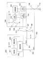
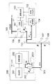
- FIG. 1 is a configuration diagram of a physical quantity detection device 100 and a sensor 200 according to Embodiment 1.
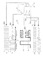
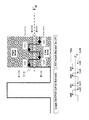
- FIG. It is a figure which shows the voltage level of each signal transmitted / received between the physical quantity detection apparatus 100 and the sensor 200.
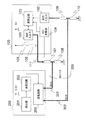
- FIG. It is a figure explaining operation
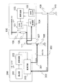
- FIG. It is a figure explaining the operation
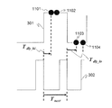
- FIG. 10 is a diagram for explaining timing when the arithmetic circuit 103 samples the data signal SDA301 in the fourth embodiment.
- FIG. 1 is a configuration diagram of a physical quantity detection device 100 and a sensor 200 according to Embodiment 1 of the present invention.
- the physical quantity detection device 100 is a device that receives the detection result of the physical quantity detected by the sensor 200 via the I2C bus 300 and acquires the detection result.
- the physical quantity detection device 100 can be configured by a microcomputer including an arithmetic circuit 103 such as a CPU (Central Processing Unit), but is not limited to this as long as it has an equivalent function.
- a microcomputer including an arithmetic circuit 103 such as a CPU (Central Processing Unit), but is not limited to this as long as it has an equivalent function.
- CPU Central Processing Unit
- the physical quantity detection device 100 is a device that operates using a power supply voltage of 5 V, and includes general-purpose input / output circuits 101 and 102, an arithmetic circuit 103, an A / D converter 104, a switch 105, a pull-up resistor 106, and a data voltage dividing resistor. 107 and 108 and clock voltage dividing resistors 109 and 110 are provided.
- the general-purpose input / output circuit 101 is a circuit for transmitting and receiving a data signal SDA301, which will be described later, to and from the sensor 200, and can switch between input and output in accordance with a command from the arithmetic circuit 103.
- the switch 105 is turned on, and the pull-up resistor 106 and the 5V power source are connected.
- the general-purpose input / output circuit 102 is a circuit for transmitting and receiving a clock signal SCK302 described later to and from the sensor 200, and can switch between input and output in accordance with a command from the arithmetic circuit 103.
- the arithmetic circuit 103 includes an arithmetic unit that performs a logical operation such as a CPU, for example, and transmits a data signal SDA 301 to the sensor 200 via the general-purpose input / output circuit 101 and the sensor via the general-purpose input / output circuit 102.
- a clock signal SCK 302 is transmitted to 200.
- the data signal SDA 301 is received from the sensor 200 via the general-purpose input / output circuit 101 and the A / D converter 104.
- the A / D converter 104 is connected to the sensor 200 in parallel with the general-purpose input / output circuit 101, converts the voltage level of the data signal SDA301 transmitted by the sensor 200 into a numerical value, and outputs the numerical value to the arithmetic circuit 103.
- the general purpose input / output circuit 101 transmits the data signal SDA301 to the sensor 200
- the data signal SDA301 is also input to the A / D converter 104.
- the pull-up resistor 106 is connected to the power supply of the physical quantity detection device 100 when the switch 105 is turned on. As a result, the data signal SDA301 transmitted by the sensor 200 is pulled up.
- Such a built-in pull-up resistor is a function that is typically provided in recent microcomputers. Since the pull-up resistor 106 is a resistor manufactured using a semiconductor process, the resistance value is generally about several tens of k ⁇ .
- the data voltage dividing resistors 107 and 108 are resistors for dividing the voltage level when the data signal SDA301 is transmitted from the physical quantity detection device 100 to the sensor 200.
- the clock voltage dividing resistors 109 and 110 are resistors for dividing the voltage level when transmitting the clock signal SCK302 from the physical quantity detection device 100 to the sensor 200.
- the physical quantity detection device 100 and the sensor 200 are grounded to the same potential via the data voltage dividing resistors 107 and 108 and the clock voltage dividing resistors 109 and 110.
- the sensor 200 is a device that operates using a power supply voltage of 2.5 V, for example, lower than the power supply voltage of the physical quantity detection device 100, and is electrically connected to the physical quantity detection device 100 via the I2C bus 300.
- the sensor 200 includes a detection unit 201, an arithmetic circuit 202, and a communication circuit 203.
- the detection unit 201 is an element that detects a physical quantity and converts the result into an electric signal or the like.
- the arithmetic circuit 202 converts the detection result of the detection unit 201 into digital data by, for example, pulse modulation, and transmits the data to the physical quantity detection device 100 as the data signal SDA301 via the communication circuit 203 and the I2C bus 300.
- I2C communication it is desirable for both the transmission and reception sides to communicate under the same power supply voltage.
- a low voltage circuit such as a sensor
- the digital circuit such as the arithmetic circuit 103 uses the Hi level threshold and the Lo level threshold determined by the operating voltage to determine the logic level of the communication signal, that is, whether the signal is a high level signal or a low level signal. This is because it is determined.
- These threshold values are the first Hi level threshold value and the first Lo level threshold value as the determination threshold values originally provided in the arithmetic circuit 103.
- the clock signal SCK302 is always a signal output from the physical quantity detection device 100 to the sensor 200. Therefore, by dividing the voltage level of the clock signal SCK302 by the clock voltage dividing resistors 109 and 110, a desired signal for the sensor 200 is obtained. It can be converted to a voltage level. This is because the physical quantity detection device 100 operates at a higher power supply voltage than the sensor 200.
- the data signal SDA301 which is a bidirectional data signal, can be converted to a voltage level desired by the sensor 200 by dividing the voltage level by the data voltage dividing resistors 107 and 108.
- FIG. 2 is a diagram showing the voltage level of each signal transmitted and received between the physical quantity detection device 100 and the sensor 200.
- the right diagram in FIG. 2 is a schematic diagram of FIG. 1
- the upper left diagram in FIG. 2 is a signal waveform at a position closer to the physical quantity detection device 100 than each voltage dividing resistor
- the lower left diagram in FIG. 2 is closer to the sensor 200 than each voltage dividing resistor.
- the signal waveform at the position, and the middle left diagram of FIG. 2 is an enlarged view of a portion surrounded by a circle in the upper left diagram.
- the clock signal SCK 302 is transmitted from the physical quantity detection device 100 to the sensor 200. Although the voltage level at the time of transmission is 5V, the voltage is reduced by the clock voltage dividing resistors 109 and 110, and when reaching the sensor 200, the operating voltage of the sensor 200 is 2.5V. The same applies to the data signal SDA301. However, the data signal SDA301 may be transmitted from the sensor 200 to the physical quantity detection device 100. Since the voltage level at the time when the data signal SDA301 arrives at the terminal 111 is an intermediate value between the first Hi level threshold VIH and the first Lo level threshold VIL, the arithmetic circuit 103 identifies the logical value of the data signal SDA301 as it is. Can not. The details of FIG. 2 will be further described below.
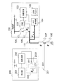
- FIG. 3 is a diagram for explaining the operation when a command is transmitted from the physical quantity detection device 100 to the sensor 200.
- a path indicated by a thick line in FIG. 3 indicates a path through which a signal is transmitted and received in the drawing.
- the arithmetic circuit 103 transmits serial data to the sensor 200 by operating the potential of the data signal SDA301 in synchronization with the signal edge of the clock signal SCK302. Since the clock signal SCK302 is always output from the physical quantity detection device 100, if the 5V clock signal SCK302 is output from the general-purpose input / output circuit 102, the divided clock signal SCK302 is always the operating voltage amplitude on the sensor 200 side (this embodiment). In Mode 1, it operates at around 2.5 V). Similarly, if the data signal SDA301 is output from the general-purpose input / output circuit 101 at a voltage level of 5V, the sensor 200 side has an amplitude of about 2.5V, and the sensor 200 can receive the command without any problem.
- FIG. 4 is a diagram for explaining the operation when the detection result is transmitted from the sensor 200 to the physical quantity detection device 100 as the data signal SDA301.
- a path indicated by a thick line in FIG. 4 indicates a path through which a signal is transmitted and received in the drawing.
- the SDA terminal of the communication circuit 203 is switched to the output terminal, and the general-purpose input / output circuit 101 is switched to the input in preparation for reception of the data signal SDA301.
- the arithmetic circuit 103 turns on the switch 105 to connect the pull-up resistor 106 to the terminal 111, and the data signal. Pull up the voltage level of SDA301.
- the output circuit of the communication circuit 203 is, for example, an open drain (collector), and has only a function of connecting the output terminal to the ground side. Therefore, it is the pull-up resistor 106 that raises the voltage level of the data signal SDA301. According to this configuration, the voltage level of the data signal SDA301 can be changed by the communication circuit 203 driving the data signal SDA301 by open drain.
- FIG. 5 is a diagram illustrating a circuit state when the sensor 200 outputs the Lo level data signal SDA301.
- the output terminal is an open drain circuit, and the transistor 2031 is connected to the ground side.
- the circuit resistance of the transistor 2031 is Rpd.
- the resistance value of the data voltage dividing resistors 107 and 108 is R.
- the potential V in_lo of the terminal 111 is expressed by the following formula 1.
- the resistance values of the data voltage dividing resistors 107 and 108 are set to the same value. If the signal amplitude of the data signal SDA301 falls within the operable range of the physical quantity detection device 100 when transmitting the signal SDA301, the present invention is not limited to this.
- FIG. 6 is a diagram showing a circuit state when the sensor 200 outputs the Hi level data signal SDA301.
- the communication circuit 203 has an open output terminal, and the potential of the data signal SDA301 does not depend on the sensor 200 side.
- the potential V in_hi of the terminal 111 at this time is a potential divided by the pull-up resistor 106 and the data voltage dividing resistors 107 and 108, and is expressed by the following formula 2.
- Equations 1 and 2 there is no constant that satisfies the Hi level threshold value VIH and the Lo level threshold value VIL of the arithmetic circuit 103 no matter what value the data voltage dividing resistors 107 and 108 whose parameters can be changed practically. . That is, the data signal SDA301 cannot be used for bidirectional communication only with the circuit configuration shown in FIG.
- the first Hi level threshold value VIH and the first Lo level threshold value VIL are used, and when a signal is transmitted from the sensor 200 to the physical quantity detection device 100.
- the second Hi level threshold and the second Lo level threshold determined on the software are used.
- the terminal 111 of the general-purpose input / output circuit 101 and the A / D converter 104 are connected in parallel to the sensor 200, and signals are transmitted and received between the physical quantity detection device 100 and the sensor 200. Are also input to the A / D converter 104.
- the A / D converter 104 is simply connected when transmitting a signal from the physical quantity detection device 100 to the sensor 200.
- the A / D converter 104 A / D converts the potential of the data signal SDA301 in synchronization with the timing at which the arithmetic circuit 103 operates the clock signal SCK302. Is converted into a numerical value and output to the arithmetic circuit 103.
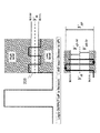
- FIG. 7 is a diagram illustrating how the Hi / Lo level of a signal is determined using the second Hi level threshold VIH and the second Lo level threshold VIL set by the arithmetic circuit 103 in the arithmetic processing.
- the arithmetic circuit 103 is a Hi level signal if the value converted into a numerical value by the A / D converter 104 is larger than the second Hi level threshold VIH, and if the value is smaller than the second Lo level threshold VIL, the signal is a Lo level signal. It is determined that
- the second Hi level threshold value VIH and the second Lo level threshold value VIL as shown in FIG. 7 are implemented by software, it takes a certain amount of time for the determination process for comparing each threshold value with the data signal SDA301 received from the sensor 200.
- the data signal SDA301 transmitted from the sensor 200 changes in synchronization with the clock signal SCK302 output from the arithmetic circuit 103, if the timing of the clock signal SCK302 is manipulated in accordance with the software determination processing, The logical value of the data signal SDA301 is not affected by the timing of the clock signal SCK302. That is, the physical quantity detection device 100 can receive the correct data signal SDA301 from the sensor 200.
- the threshold value on the software can be set arbitrarily, it can be flexibly adapted to the difference in operating voltage between the sensor 200 and the physical quantity detection device 100, the resistance value of the pull-up resistor 106, and any other combination of parameters.
- the physical quantity detection device 100 when receiving the data signal SDA301 from the sensor 200, the physical quantity detection device 100 according to the first embodiment replaces the first Hi level threshold and the first Lo level threshold with the second Hi level set in software processing.
- the Hi / Lo level of the data signal SDA301 is determined using the threshold and the second Lo level threshold.
- the communication can be realized only with the resistor and the software, the reliability of the circuit can be improved, and the influence due to variations in the resistor and circuit characteristics can be reduced. As a result, the entire device can be constructed at low cost and high reliability can be obtained.
- the arithmetic circuit 103 determines the Hi / Lo level of the data signal SDA301 using the Hi / Lo level threshold set on the software.
- the threshold for determining the Hi / Lo level is changed according to the voltage level fluctuation of the data signal SDA301. Since the configuration of each device is the same as that of the first embodiment, the following description will focus on differences.
- FIG. 8 shows the relationship between V in_hi and V in_lo when the pull-up resistor 106, each voltage dividing resistor, the reference voltage of the A / D converter 104, etc. fluctuate due to individual differences in components, temperature changes, deterioration with time, and the like.
- FIG. The vertical axis schematically shows the potential of the terminal 111 (A / D converted voltage), and the horizontal axis schematically shows the amount of change of each parameter due to temperature change or individual difference.
- a characteristic 1101 indicates a variation in the reference voltage of the A / D converter 104, and this value is also involved as an error factor when performing a logical determination by software.
- the optimum threshold value varies depending on the change of the circuit constant, and varies even during the operation of the physical quantity detection device 100 and the sensor 200 due to external factors such as temperature. Since the difference between V in_hi and the voltage V in_lo described in the first embodiment is as small as about 1V, there is a possibility of erroneous determination when performing logical determination by software with a single threshold. Therefore, as shown in FIG. 8, it is considered desirable to change the recommended software threshold value V th in accordance with the variation of V in_hi and V in_lo . Although it is conceivable to change both the second Hi level threshold value VIH and the second Lo level threshold value VIL, in the first embodiment, the Hi / Lo level is determined by a single threshold value V th .
- FIG. 9 illustrates a procedure for calculating the threshold value V th .
- the arithmetic circuit 103 individually records the A / D conversion results of the high level data signal SDA301 and the low level data signal SDA301.
- the recording destination may be a storage device such as a memory provided in the arithmetic circuit 103, for example.
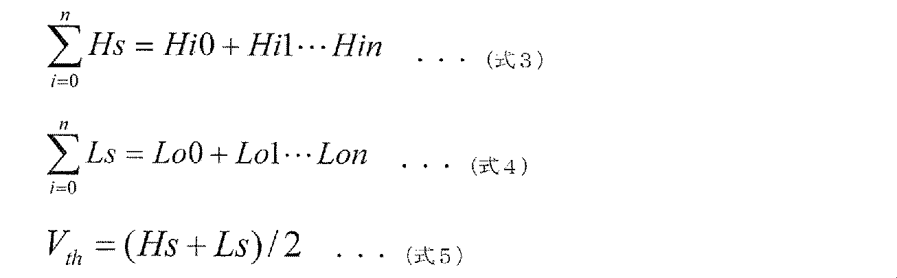
- the arithmetic circuit 103 adds these recorded values as shown in the following formulas 3 and 4, respectively, and independently performs smoothing processing (for example, moving average, arithmetic average, weighted average, square average, etc.).
- the arithmetic circuit 103 calculates a threshold value V th as an intermediate value between V in_hi and V in_lo according to the following equation (5).
- V in_hi and V in_lo are stored in the buffer and averaged. However, a single buffer that records only the previous value may be used. Further, a difference between V in_hi and V in_lo may be learned, and an intermediate value between them may be set as a threshold value V th , or learning may be performed only at startup.
- the physical quantity detection device 100 accumulates the data signal SDA301 for each past Hi / Lo level as the threshold value Vth for determining the Hi / Lo level of the data signal SDA301. Calculate by averaging. Thereby, even if V in_hi and V in_lo fluctuate due to factors such as temperature change, it is possible to always determine the Hi / Lo level with the optimum threshold.
- the Hi / Lo level is determined using a single threshold value V th .
- V th a threshold value
- an operation example in which a dead zone is provided above and below the threshold V th and a communication error occurs when the A / D conversion result of the data signal SDA301 is in the dead zone will be described. Since the configuration of each device is the same as in the first and second embodiments, the following description will focus on differences.
- FIG. 10 is a diagram illustrating a procedure for calculating the dead zone in the third embodiment.
- the dead zone can be calculated by vertically offsetting the threshold value V th described in the second embodiment. More specifically, the present invention may calculate the offset width V ofs_hi / lo in accordance with the value of the threshold V th as shown in the following formula 6, a difference V pp of V In_hi and V In_lo as shown in the following formula 7 Depending on, the offset width V ofs_hi / lo may be calculated.
- the function f, offset width V ofs_hi / lo the threshold V th or difference V pp is smaller decreases in constructed functions as the threshold V th or difference V pp is greater offset width V ofs_hi / lo is greater is there.
- the arithmetic circuit 103 processes the signal as a communication error.
- FIG. 11 is a diagram illustrating the timing at which the arithmetic circuit 103 samples the data signal SDA301 in the fourth embodiment.
- Black circles 1101 and 1102 indicate the timing at which the Hi-level data signal SDA301 is sampled.
- Black circles 1103 and 1104 indicate the timing at which the Lo level data signal SDA301 is sampled.
- the delay T dly_hi is a delay time from the falling timing of the clock signal SCK302 to the timing at which the arithmetic circuit 103 samples the Hi-level data signal SDA301.
- the delay T dly_lo is a delay time from the falling timing of the clock signal SCK302 to the timing at which the arithmetic circuit 103 samples the Lo level data signal SDA301.
- the arithmetic circuit 103 samples the data signal SDA301 at the falling timing of the clock signal SCK302, but the rising edge of the data signal SDA301 becomes dull due to the influence of the parasitic capacitance of the circuit. In such a case, it may be desirable to perform sampling with a slight delay from the falling timing of the clock signal SCK302. Therefore, in the fourth embodiment, the delays T dly_hi and T dly_lo are provided.
- the reason why two types of delay time are provided is that the influence of the resistance value and the parasitic capacitance on the waveform of the data signal SDA301 differs between the Hi level signal and the Lo level signal. Therefore, two types of delay times are provided so that the timing for sampling the Hi level signal and the timing for sampling the Lo level data signal are different from each other.
- the arithmetic circuit 103 performs sampling two or more times. (A) When both are at the Hi level, it is determined that the signal is a Hi level signal, and (b) when both are at the Lo level. It is determined that the signal is a Lo level signal, and (c) if the Hi / Lo levels do not match each other, it is processed as a communication error.
- the sampling interval (for example, the interval between the black circles 1101 and 1102) from the next time onward may be increased to improve sampling reliability. The same effect can be exhibited even if the sampling frequency is lowered after the next time.
- the physical quantity detection device 100 performs sampling a plurality of times on the data signal SDA301 having the same value, compares the sampling results of each time, and adjusts the sampling timing. Thereby, even when the waveform of the data signal SDA301 is dull, the value of the data signal SDA301 can be reliably acquired by appropriately setting the sampling timing.
- the physical quantity detection device 100 and the sensor 200 communicate using the I2C communication method.
- the present invention is different from the present invention.
- the same effect can be exhibited.
- the voltage level of the communication signal is lowered using the voltage dividing resistor, the same function can be exhibited even if a circuit or the like that can lower the voltage level is used.
- each of the above-described configurations, functions, processing units, etc. can be realized as hardware by designing all or a part thereof, for example, with an integrated circuit, or the processor executes a program for realizing each function. By doing so, it can be realized as software.
- Information such as a program and a table for realizing each function can be stored in a storage device such as a memory or a hard disk, or a storage medium such as an IC card or a DVD.
- 100 physical quantity detection device
- 101 and 102 general-purpose input / output circuit
- 103 arithmetic circuit
- 104 A / D converter
- 105 switch
- 106 pull-up resistor
- 107 and 108 data voltage dividing resistor
- 109 and 110 Clock voltage dividing resistor
- 202 arithmetic circuit
- 203 communication circuit
- 301 data signal SDA
- 302 clock signal SCK.
Landscapes
- Engineering & Computer Science (AREA)
- Computer Hardware Design (AREA)
- Physics & Mathematics (AREA)
- Computing Systems (AREA)
- General Engineering & Computer Science (AREA)
- Mathematical Physics (AREA)
- General Physics & Mathematics (AREA)
- Arrangements For Transmission Of Measured Signals (AREA)
- Logic Circuits (AREA)
Abstract
Description
図1は、本発明の実施形態1に係る物理量検出装置100およびセンサ200の構成図である。物理量検出装置100は、センサ200が検出した物理量の検出結果を、I2Cバス300を介して受信し、その検出結果を取得する装置である。物理量検出装置100は、例えばCPU(Central Processing Unit)などの演算回路103を搭載したマイコンによって構成することができるが、同等の機能を備えていればこれに限られるものではない。


以上のように、本実施形態1に係る物理量検出装置100は、センサ200からデータ信号SDA301を受信するときは、第1Hiレベル閾値と第1Loレベル閾値に代えてソフトウェア処理上で設定した第2Hiレベル閾値と第2Loレベル閾値を用いて、データ信号SDA301のHi/Loレベルを判定する。これにより、汎用的なマイコンが通常備えている機能と抵抗器のみで、電源電圧の異なるセンサ200との間で双方向通信をすることができる。したがって、特許文献1に記載されているような半導体を用いた双方向レベルコンバーターが不要となり、安価に通信回路を構成できる。また、抵抗器とソフトウェアだけで通信が実現できるため回路の信頼性を高めることができ、抵抗器や回路特性のばらつきによる影響も低減することができる。ひいては機器全体を安価に構成し、高い信頼性を得ることができる。
実施形態1では、演算回路103がソフトウェア上で設定したHi/Loレベル閾値を用いて、データ信号SDA301のHi/Loレベルを判定することを説明した。本発明の実施形態2では、データ信号SDA301の電圧レベル変動に応じて、Hi/Loレベルを判定するための閾値を変化させる動作例を説明する。各機器の構成は実施形態1と同様であるため、以下では差異点を中心に説明する。
以上のように、本実施形態2に係る物理量検出装置100は、データ信号SDA301のHi/Loレベルを判定するための閾値Vthを、過去のHi/Loレベルそれぞれのデータ信号SDA301を蓄積して平均することにより計算する。これにより、温度変化などの要因によってVin_hiとVin_loが変動しても、常に最適な閾値でHi/Loレベルを判定することができる。
実施形態2では単一の閾値Vthを用いてHi/Loレベルを判定することを説明した。本発明の実施形態3では、閾値Vthの上下に不感帯を設け、データ信号SDA301のA/D変換結果が不感帯に入っている場合は通信エラーとする動作例を説明する。各機器の構成は実施形態1~2と同様であるため、以下では差異点を中心に説明する。

以上のように、本実施形態3に係る物理量検出装置100によれば、不感帯を設けることによってさらに柔軟な論理判定が可能になり、電気的ノイズなどの外乱に対する冗長性が確保できる。また、Vppの値を評価することで信号が十分な振幅を持っているかなどの診断も可能になり、センサ全体としての故障検出性能を向上することができる。これら不感帯の大きさや計算方法が変わっても本発明の効果は同様である。
本発明の実施形態4では、演算回路103がデータ信号SDA301をサンプリングするタイミングを調整する動作例について説明する。各機器の構成は実施形態1~3と同様であるため、以下では差異点を中心に説明する。
以上のように、本実施形態4に係る物理量検出装置100は、同じ値のデータ信号SDA301に対してサンプリングを複数回実施し、各回のサンプリング結果を比較してサンプリングタイミングを調整する。これにより、データ信号SDA301の波形が鈍っている場合でも、サンプリングタイミングを適切に設定することにより確実にデータ信号SDA301の値を取得することができる。
以上、本発明者によってなされた発明を実施形態に基づき具体的に説明したが、本発明は前記実施の形態に限定されるものではなく、その要旨を逸脱しない範囲で種々変更可能であることは言うまでもない。
Claims (14)
- 物理量を検出するセンサとの間で双方向に通信する通信線と、
前記センサよりも高い動作電圧で動作し、前記センサが検出した物理量の値を前記通信線経由で取得する論理回路と、
前記センサとの間で信号を送受信する入出力回路と、
前記入出力回路が受信した信号を数値に変換するA/D変換器と、
前記論理回路が前記通信線を介して前記センサに対して出力する信号の電圧を減圧する減圧回路と、
を備え、
前記論理回路は、
所定の第1Hiレベル閾値と第1Loレベル閾値にしたがって、前記A/D変換器が数値に変換した前記信号がHiレベル信号であるかLoレベル信号であるかを判定する演算器を備え、
前記入出力回路と前記A/D変換器は、
前記センサに対して互いに並列に接続されており、
前記演算器は、
前記通信線を介して前記物理量を記述した信号を前記センサから受信する際には、
前記第1Hiレベル閾値と前記第1Loレベル閾値に代えて、前記演算器が実施する演算処理上で定められた第2Hiレベル閾値と第2Loレベル閾値にしたがって、前記A/D変換器が数値に変換した前記信号がHiレベル信号であるかLoレベル信号であるかを判定することにより、前記センサが送信した前記物理量の値を取得する
ことを特徴とする物理量検出装置。 - 前記演算器は、前記第2Hiレベル閾値と前記第2Loレベル閾値を異なる値とする
ことを特徴とする請求項1記載の物理量検出装置。 - 前記演算器は、
前記センサから受信するHiレベル信号とLoレベル信号をそれぞれ記録し、
記録された前記Hiレベル信号と前記Loレベル信号の間の値を、前記第2Hiレベル閾値、前記第2Loレベル閾値、または前記第2Hiレベル閾値と前記第2Loレベル閾値を兼ねた閾値として用いる
ことを特徴とする請求項1記載の物理量検出装置。 - 前記演算器は、
前記記録されたHiレベル信号とLoレベル信号の移動平均、相加平均、加重平均、または二乗平均を、前記第2Hiレベル閾値と前記第2Loレベル閾値を兼ねた閾値として用いる
ことを特徴とする請求項3記載の物理量検出装置。 - 前記演算器は、
前記記録されたHiレベル信号とLoレベル信号の中間値を計算し、
前記中間値にオフセットを加算した値を前記第2Hiレベル閾値とし、
前記中間値からオフセットを減算した値を前記第2Loレベル閾値とする
ことを特徴とする請求項3記載の物理量検出装置。 - 前記演算器は、前記記録されたHiレベル信号とLoレベル信号の間の差分の絶対値が大きいほど前記オフセットを大きくする
ことを特徴とする請求項5記載の物理量検出装置。 - 前記演算器は、
前記A/D変換器が数値に変換した結果が前記第2Hiレベル閾値と前記第2Loレベル閾値の間にある場合は、前記センサから前記信号を受信できなかったものとする
ことを特徴とする請求項5記載の物理量検出装置。 - 前記演算器は、
前記センサから前記信号を受信する際に、同じ値に対するサンプリングを、互いに異なるタイミングで複数回実施する
ことを特徴とする請求項1記載の物理量検出装置。 - 前記演算器は、
前記センサが送信したHiレベル信号をサンプリングする際の前記タイミングと、前記センサが送信したLoレベル信号をサンプリングする際の前記タイミングを、互いに異なるタイミングとする
ことを特徴とする請求項8記載の物理量検出装置。 - 前記演算器は、
各回の前記サンプリングによって取得した前記信号間の差分が所定値以上である場合は、前記タイミングを一時的に遅らせ、または前記サンプリングの周波数を一時的に下げて前記サンプリングを再試行する
ことを特徴とする請求項8記載の物理量検出装置。 - 前記演算器は、前記複数回のサンプリングの結果が互いに異なる場合は、前記センサから前記信号を受信できなかったものとする
ことを特徴とする請求項8記載の物理量検出装置。 - 前記論理回路は、前記A/D変換器の入力端子と、前記論理回路の動作電源との間に接続されたプルアップ抵抗器を備えており、
前記減圧回路は、一端が前記プルアップ抵抗器に接続され、他端が接地されている
ことを特徴とする請求項1記載の物理量検出装置。 - 前記減圧回路は、前記センサと前記論理回路の間に配置された分圧抵抗として構成されている
ことを特徴とする請求項1記載の物理量検出装置。 - 前記論理回路は、I2C方式を用いて前記センサとの間で通信する
ことを特徴とする請求項1記載の物理量検出装置。
Priority Applications (3)
| Application Number | Priority Date | Filing Date | Title |
|---|---|---|---|
| US14/354,154 US9383232B2 (en) | 2012-01-16 | 2012-12-07 | Physical quantity detection device |
| CN201280066813.XA CN104040893B (zh) | 2012-01-16 | 2012-12-07 | 物理量检测装置 |
| DE112012005680.9T DE112012005680T5 (de) | 2012-01-16 | 2012-12-07 | Detektionsvorrichtung für physikalische Größen |
Applications Claiming Priority (2)
| Application Number | Priority Date | Filing Date | Title |
|---|---|---|---|
| JP2012006536A JP5680572B2 (ja) | 2012-01-16 | 2012-01-16 | 物理量検出装置 |
| JP2012-006536 | 2012-01-16 |
Publications (1)
| Publication Number | Publication Date |
|---|---|
| WO2013108505A1 true WO2013108505A1 (ja) | 2013-07-25 |
Family
ID=48798942
Family Applications (1)
| Application Number | Title | Priority Date | Filing Date |
|---|---|---|---|
| PCT/JP2012/081734 Ceased WO2013108505A1 (ja) | 2012-01-16 | 2012-12-07 | 物理量検出装置 |
Country Status (5)
| Country | Link |
|---|---|
| US (1) | US9383232B2 (ja) |
| JP (1) | JP5680572B2 (ja) |
| CN (1) | CN104040893B (ja) |
| DE (1) | DE112012005680T5 (ja) |
| WO (1) | WO2013108505A1 (ja) |
Families Citing this family (10)
| Publication number | Priority date | Publication date | Assignee | Title |
|---|---|---|---|---|
| JP6311871B2 (ja) * | 2014-04-17 | 2018-04-18 | セイコーエプソン株式会社 | 物理量検出用回路、物理量検出装置、物理量計測システム、電子機器、移動体及び物理量計測データ生成方法 |
| JP6428287B2 (ja) * | 2015-01-19 | 2018-11-28 | 株式会社ジェイテクト | データ送受信装置 |
| CN107769867B (zh) * | 2016-08-15 | 2021-06-25 | 中兴通讯股份有限公司 | 一种物理量指示方法、装置、系统及物理量指示设备 |
| CH714256A1 (de) * | 2017-10-18 | 2019-04-30 | Elesta Gmbh Ostfildern De Zweigniederlassung Bad Ragaz | Verfahren zur seriellen Übermittlung von Daten eines Sensors an ein Sicherheitskontrollgerät. |
| WO2019147216A1 (en) | 2018-01-23 | 2019-08-01 | Hewlett-Packard Development Company, L.P. | Direct current drive circuitry devices |
| US12031970B2 (en) | 2020-04-30 | 2024-07-09 | Precision Planting Llc | Agricultural sampling system and related methods |
| US12345697B2 (en) | 2020-04-30 | 2025-07-01 | Precision Planting Llc | Agricultural sampling system and related methods |
| EP4002703B1 (en) * | 2020-11-11 | 2024-10-09 | Aptiv Technologies AG | Bidirectional communication circuit, system and method for bidirectional communication |
| US12673278B2 (en) | 2021-05-20 | 2026-07-07 | Precision Planting Llc | Agricultural sampling system and related methods |
| CN116981942A (zh) | 2021-06-09 | 2023-10-31 | 精密种植有限责任公司 | 微型泵 |
Citations (4)
| Publication number | Priority date | Publication date | Assignee | Title |
|---|---|---|---|---|
| JP2002185293A (ja) * | 2000-12-08 | 2002-06-28 | Sumitomo Wiring Syst Ltd | マイコンの入力回路 |
| JP2008016941A (ja) * | 2006-07-03 | 2008-01-24 | Nec Access Technica Ltd | データ転送システムおよびi2c通信方法 |
| JP2010068321A (ja) * | 2008-09-11 | 2010-03-25 | Fujitsu Ltd | I2cインタフェースを有するシステム及びその方法 |
| WO2012157031A1 (ja) * | 2011-05-13 | 2012-11-22 | パナソニック株式会社 | 信号電位変換回路 |
Family Cites Families (4)
| Publication number | Priority date | Publication date | Assignee | Title |
|---|---|---|---|---|
| JP4101518B2 (ja) * | 2000-05-02 | 2008-06-18 | 株式会社日立製作所 | 空気流量計 |
| JP2003133937A (ja) | 2001-10-23 | 2003-05-09 | Funai Electric Co Ltd | 双方向レベルコンバータ回路 |
| JP2010133767A (ja) * | 2008-12-03 | 2010-06-17 | Epson Toyocom Corp | 物理量検出装置 |
| JP5281556B2 (ja) * | 2009-12-07 | 2013-09-04 | セイコーインスツル株式会社 | 物理量センサ |
-
2012
- 2012-01-16 JP JP2012006536A patent/JP5680572B2/ja not_active Expired - Fee Related
- 2012-12-07 DE DE112012005680.9T patent/DE112012005680T5/de not_active Withdrawn
- 2012-12-07 CN CN201280066813.XA patent/CN104040893B/zh not_active Expired - Fee Related
- 2012-12-07 WO PCT/JP2012/081734 patent/WO2013108505A1/ja not_active Ceased
- 2012-12-07 US US14/354,154 patent/US9383232B2/en not_active Expired - Fee Related
Patent Citations (4)
| Publication number | Priority date | Publication date | Assignee | Title |
|---|---|---|---|---|
| JP2002185293A (ja) * | 2000-12-08 | 2002-06-28 | Sumitomo Wiring Syst Ltd | マイコンの入力回路 |
| JP2008016941A (ja) * | 2006-07-03 | 2008-01-24 | Nec Access Technica Ltd | データ転送システムおよびi2c通信方法 |
| JP2010068321A (ja) * | 2008-09-11 | 2010-03-25 | Fujitsu Ltd | I2cインタフェースを有するシステム及びその方法 |
| WO2012157031A1 (ja) * | 2011-05-13 | 2012-11-22 | パナソニック株式会社 | 信号電位変換回路 |
Also Published As
| Publication number | Publication date |
|---|---|
| CN104040893B (zh) | 2017-04-26 |
| JP5680572B2 (ja) | 2015-03-04 |
| CN104040893A (zh) | 2014-09-10 |
| JP2013146035A (ja) | 2013-07-25 |
| US9383232B2 (en) | 2016-07-05 |
| US20140298930A1 (en) | 2014-10-09 |
| DE112012005680T5 (de) | 2014-10-30 |
Similar Documents
| Publication | Publication Date | Title |
|---|---|---|
| JP5680572B2 (ja) | 物理量検出装置 | |
| US10129132B2 (en) | Control system, control method, control program, and recording medium | |
| CN101452370B (zh) | Oob(带外)检测电路及串行ata系统 | |
| EP2115408A1 (en) | Apparatus, system and method for high resolution identification with temperature dependent resistive device | |
| JP5053421B2 (ja) | 信号判定システム及び温度判定システム | |
| US10284192B2 (en) | Semiconductor device | |
| CN110208596B (zh) | 负载电流监测电路及方法 | |
| EP3474027A1 (en) | Method for identifying a fault at a device output and system therefor | |
| CN101594133A (zh) | 半导体集成电路、控制方法及信息处理装置 | |
| US9294078B1 (en) | Voltage-driver circuit with dynamic slew rate control | |
| CN103869142B (zh) | 用于监视信号电平的方法和设备 | |
| EP3477317A1 (en) | Method for identifying a fault at a device output and system therefor | |
| US7545149B2 (en) | Driver and receiver circuit for a remotely arranged circuit and corresponding method | |
| US11287867B2 (en) | Power sequence monitoring system | |
| JP2014062825A (ja) | 電圧検出回路及び電圧検出方法 | |
| US9824553B2 (en) | Distance detection system, vibration prompt circuit and vibration prompt method | |
| CN113330686B (zh) | 借助经脉宽调制的信号来传输值的系统及方法 | |
| EP3211508B1 (en) | Semiconductor device | |
| CN104764544A (zh) | 温度信号自我诊断电路及其诊断方法 | |
| JP7351202B2 (ja) | 異常検出装置、電気機器、画像形成装置、電気機器の異常検出方法、及び異常検出プログラム | |
| JP4835207B2 (ja) | 温度伝送器 | |
| JP2011153971A (ja) | 半導体装置及びパルス幅検出方法 | |
| JP6598928B1 (ja) | 電子制御装置 | |
| CN106597198A (zh) | 一种检测装置、方法及电子设备 | |
| US10025743B2 (en) | Semiconductor device, semiconductor system including same, and semiconductor device control method |
Legal Events
| Date | Code | Title | Description |
|---|---|---|---|
| 121 | Ep: the epo has been informed by wipo that ep was designated in this application |
Ref document number: 12865904 Country of ref document: EP Kind code of ref document: A1 |
|
| WWE | Wipo information: entry into national phase |
Ref document number: 14354154 Country of ref document: US |
|
| WWE | Wipo information: entry into national phase |
Ref document number: 1120120056809 Country of ref document: DE Ref document number: 112012005680 Country of ref document: DE |
|
| 122 | Ep: pct application non-entry in european phase |
Ref document number: 12865904 Country of ref document: EP Kind code of ref document: A1 |