EP3477317A1 - Method for identifying a fault at a device output and system therefor - Google Patents
Method for identifying a fault at a device output and system therefor Download PDFInfo
- Publication number
- EP3477317A1 EP3477317A1 EP18194194.9A EP18194194A EP3477317A1 EP 3477317 A1 EP3477317 A1 EP 3477317A1 EP 18194194 A EP18194194 A EP 18194194A EP 3477317 A1 EP3477317 A1 EP 3477317A1
- Authority
- EP
- European Patent Office
- Prior art keywords
- current
- transistor
- signal
- mirror
- threshold
- Prior art date
- Legal status (The legal status is an assumption and is not a legal conclusion. Google has not performed a legal analysis and makes no representation as to the accuracy of the status listed.)
- Granted
Links
- 238000000034 method Methods 0.000 title claims description 30
- 230000007704 transition Effects 0.000 claims description 14
- 230000002950 deficient Effects 0.000 claims description 4
- 230000007547 defect Effects 0.000 claims description 2
- 239000003990 capacitor Substances 0.000 description 23
- 238000010586 diagram Methods 0.000 description 18
- 238000001514 detection method Methods 0.000 description 11
- 230000008901 benefit Effects 0.000 description 8
- 230000008569 process Effects 0.000 description 5
- 230000000694 effects Effects 0.000 description 4
- 230000003071 parasitic effect Effects 0.000 description 4
- 238000012360 testing method Methods 0.000 description 4
- 230000009471 action Effects 0.000 description 3
- 238000005516 engineering process Methods 0.000 description 3
- 239000002184 metal Substances 0.000 description 3
- 239000004020 conductor Substances 0.000 description 2
- 230000003111 delayed effect Effects 0.000 description 2
- 238000012986 modification Methods 0.000 description 2
- 230000004048 modification Effects 0.000 description 2
- 238000009966 trimming Methods 0.000 description 2
- 230000004913 activation Effects 0.000 description 1
- 230000002547 anomalous effect Effects 0.000 description 1
- 238000004891 communication Methods 0.000 description 1
- 230000009849 deactivation Effects 0.000 description 1
- 230000001934 delay Effects 0.000 description 1
- 230000001419 dependent effect Effects 0.000 description 1
- 238000013461 design Methods 0.000 description 1
- 230000005669 field effect Effects 0.000 description 1
- 238000012545 processing Methods 0.000 description 1
- 230000000644 propagated effect Effects 0.000 description 1
- 230000001105 regulatory effect Effects 0.000 description 1
- 230000004044 response Effects 0.000 description 1
- 238000000638 solvent extraction Methods 0.000 description 1
Images


Classifications
-
- G—PHYSICS
- G01—MEASURING; TESTING
- G01R—MEASURING ELECTRIC VARIABLES; MEASURING MAGNETIC VARIABLES
- G01R31/00—Arrangements for testing electric properties; Arrangements for locating electric faults; Arrangements for electrical testing characterised by what is being tested not provided for elsewhere
- G01R31/28—Testing of electronic circuits, e.g. by signal tracer
- G01R31/317—Testing of digital circuits
- G01R31/3181—Functional testing
- G01R31/3185—Reconfiguring for testing, e.g. LSSD, partitioning
- G01R31/318533—Reconfiguring for testing, e.g. LSSD, partitioning using scanning techniques, e.g. LSSD, Boundary Scan, JTAG
- G01R31/318536—Scan chain arrangements, e.g. connections, test bus, analog signals
- G01R31/318538—Topological or mechanical aspects
-
- G—PHYSICS
- G05—CONTROLLING; REGULATING
- G05F—SYSTEMS FOR REGULATING ELECTRIC OR MAGNETIC VARIABLES
- G05F1/00—Automatic systems in which deviations of an electric quantity from one or more predetermined values are detected at the output of the system and fed back to a device within the system to restore the detected quantity to its predetermined value or values, i.e. retroactive systems
- G05F1/10—Regulating voltage or current
- G05F1/46—Regulating voltage or current wherein the variable actually regulated by the final control device is dc
- G05F1/56—Regulating voltage or current wherein the variable actually regulated by the final control device is dc using semiconductor devices in series with the load as final control devices
- G05F1/575—Regulating voltage or current wherein the variable actually regulated by the final control device is dc using semiconductor devices in series with the load as final control devices characterised by the feedback circuit
-
- G—PHYSICS
- G01—MEASURING; TESTING
- G01R—MEASURING ELECTRIC VARIABLES; MEASURING MAGNETIC VARIABLES
- G01R31/00—Arrangements for testing electric properties; Arrangements for locating electric faults; Arrangements for electrical testing characterised by what is being tested not provided for elsewhere
- G01R31/28—Testing of electronic circuits, e.g. by signal tracer
- G01R31/30—Marginal testing, e.g. by varying supply voltage
- G01R31/3004—Current or voltage test
-
- G—PHYSICS
- G01—MEASURING; TESTING
- G01R—MEASURING ELECTRIC VARIABLES; MEASURING MAGNETIC VARIABLES
- G01R31/00—Arrangements for testing electric properties; Arrangements for locating electric faults; Arrangements for electrical testing characterised by what is being tested not provided for elsewhere
- G01R31/28—Testing of electronic circuits, e.g. by signal tracer
- G01R31/317—Testing of digital circuits
- G01R31/31712—Input or output aspects
- G01R31/31715—Testing of input or output circuits; test of circuitry between the I/C pins and the functional core, e.g. testing of input or output driver, receiver, buffer
-
- G—PHYSICS
- G01—MEASURING; TESTING
- G01R—MEASURING ELECTRIC VARIABLES; MEASURING MAGNETIC VARIABLES
- G01R31/00—Arrangements for testing electric properties; Arrangements for locating electric faults; Arrangements for electrical testing characterised by what is being tested not provided for elsewhere
- G01R31/28—Testing of electronic circuits, e.g. by signal tracer
- G01R31/317—Testing of digital circuits
- G01R31/31712—Input or output aspects
- G01R31/31716—Testing of input or output with loop-back
-
- G—PHYSICS
- G01—MEASURING; TESTING
- G01R—MEASURING ELECTRIC VARIABLES; MEASURING MAGNETIC VARIABLES
- G01R31/00—Arrangements for testing electric properties; Arrangements for locating electric faults; Arrangements for electrical testing characterised by what is being tested not provided for elsewhere
- G01R31/28—Testing of electronic circuits, e.g. by signal tracer
- G01R31/317—Testing of digital circuits
- G01R31/3181—Functional testing
- G01R31/3185—Reconfiguring for testing, e.g. LSSD, partitioning
- G01R31/318533—Reconfiguring for testing, e.g. LSSD, partitioning using scanning techniques, e.g. LSSD, Boundary Scan, JTAG
- G01R31/318536—Scan chain arrangements, e.g. connections, test bus, analog signals
-
- G—PHYSICS
- G01—MEASURING; TESTING
- G01R—MEASURING ELECTRIC VARIABLES; MEASURING MAGNETIC VARIABLES
- G01R31/00—Arrangements for testing electric properties; Arrangements for locating electric faults; Arrangements for electrical testing characterised by what is being tested not provided for elsewhere
- G01R31/28—Testing of electronic circuits, e.g. by signal tracer
- G01R31/317—Testing of digital circuits
- G01R31/3181—Functional testing
- G01R31/3185—Reconfiguring for testing, e.g. LSSD, partitioning
- G01R31/318533—Reconfiguring for testing, e.g. LSSD, partitioning using scanning techniques, e.g. LSSD, Boundary Scan, JTAG
- G01R31/318566—Comparators; Diagnosing the device under test
-
- G—PHYSICS
- G01—MEASURING; TESTING
- G01R—MEASURING ELECTRIC VARIABLES; MEASURING MAGNETIC VARIABLES
- G01R31/00—Arrangements for testing electric properties; Arrangements for locating electric faults; Arrangements for electrical testing characterised by what is being tested not provided for elsewhere
- G01R31/28—Testing of electronic circuits, e.g. by signal tracer
- G01R31/317—Testing of digital circuits
- G01R31/3181—Functional testing
- G01R31/3185—Reconfiguring for testing, e.g. LSSD, partitioning
- G01R31/318533—Reconfiguring for testing, e.g. LSSD, partitioning using scanning techniques, e.g. LSSD, Boundary Scan, JTAG
- G01R31/318569—Error indication, logging circuits
-
- G—PHYSICS
- G01—MEASURING; TESTING
- G01R—MEASURING ELECTRIC VARIABLES; MEASURING MAGNETIC VARIABLES
- G01R31/00—Arrangements for testing electric properties; Arrangements for locating electric faults; Arrangements for electrical testing characterised by what is being tested not provided for elsewhere
- G01R31/28—Testing of electronic circuits, e.g. by signal tracer
- G01R31/317—Testing of digital circuits
- G01R31/3181—Functional testing
- G01R31/3185—Reconfiguring for testing, e.g. LSSD, partitioning
- G01R31/318533—Reconfiguring for testing, e.g. LSSD, partitioning using scanning techniques, e.g. LSSD, Boundary Scan, JTAG
- G01R31/318572—Input/Output interfaces
-
- G—PHYSICS
- G01—MEASURING; TESTING
- G01R—MEASURING ELECTRIC VARIABLES; MEASURING MAGNETIC VARIABLES
- G01R31/00—Arrangements for testing electric properties; Arrangements for locating electric faults; Arrangements for electrical testing characterised by what is being tested not provided for elsewhere
- G01R31/28—Testing of electronic circuits, e.g. by signal tracer
- G01R31/317—Testing of digital circuits
- G01R31/3181—Functional testing
- G01R31/3185—Reconfiguring for testing, e.g. LSSD, partitioning
- G01R31/318533—Reconfiguring for testing, e.g. LSSD, partitioning using scanning techniques, e.g. LSSD, Boundary Scan, JTAG
- G01R31/318575—Power distribution; Power saving
-
- G—PHYSICS
- G01—MEASURING; TESTING
- G01R—MEASURING ELECTRIC VARIABLES; MEASURING MAGNETIC VARIABLES
- G01R31/00—Arrangements for testing electric properties; Arrangements for locating electric faults; Arrangements for electrical testing characterised by what is being tested not provided for elsewhere
- G01R31/28—Testing of electronic circuits, e.g. by signal tracer
- G01R31/317—Testing of digital circuits
- G01R31/3181—Functional testing
- G01R31/3187—Built-in tests
-
- H—ELECTRICITY
- H01—ELECTRIC ELEMENTS
- H01L—SEMICONDUCTOR DEVICES NOT COVERED BY CLASS H10
- H01L27/00—Devices consisting of a plurality of semiconductor or other solid-state components formed in or on a common substrate
- H01L27/02—Devices consisting of a plurality of semiconductor or other solid-state components formed in or on a common substrate including semiconductor components specially adapted for rectifying, oscillating, amplifying or switching and having at least one potential-jump barrier or surface barrier; including integrated passive circuit elements with at least one potential-jump barrier or surface barrier
- H01L27/0203—Particular design considerations for integrated circuits
- H01L27/0248—Particular design considerations for integrated circuits for electrical or thermal protection, e.g. electrostatic discharge [ESD] protection
- H01L27/0251—Particular design considerations for integrated circuits for electrical or thermal protection, e.g. electrostatic discharge [ESD] protection for MOS devices
- H01L27/0255—Particular design considerations for integrated circuits for electrical or thermal protection, e.g. electrostatic discharge [ESD] protection for MOS devices using diodes as protective elements
-
- H—ELECTRICITY
- H03—ELECTRONIC CIRCUITRY
- H03K—PULSE TECHNIQUE
- H03K19/00—Logic circuits, i.e. having at least two inputs acting on one output; Inverting circuits
- H03K19/20—Logic circuits, i.e. having at least two inputs acting on one output; Inverting circuits characterised by logic function, e.g. AND, OR, NOR, NOT circuits
- H03K19/21—EXCLUSIVE-OR circuits, i.e. giving output if input signal exists at only one input; COINCIDENCE circuits, i.e. giving output only if all input signals are identical
Definitions
- This disclosure relates generally to integrated circuits, and more particularly to identifying a fault at a device output.
- An electronic system can include multiple devices, such as integrated circuits.
- An electronic device can include circuitry to interface with another device.
- an integrated circuit can include an output terminal and an associated output driver for transmitting information to another integrated circuit.
- the information can be encoded and transmitted using a voltage or a current signal.
- an output driver can include push-pull circuitry to provide a signal where the information to be transmitted is encoded using discrete voltage levels corresponding to a logic-high or a logic-low state.
- an output driver can selectively enabled to sink current provided by external pull-up circuitry, where particular levels of the sink current corresponding to individual logic states.
- an output driver can provide an analog interface, in which case the output driver provides a continuously range of voltage or current instead of discrete levels.
- Faults associated with output drive circuits can be difficult to identify, especially while the electronic system is functioning in its normal operating mode.
- Faults associated with an output driver can include defective transistors in the driver circuit, broken or shorted bonding wires, damaged cables or connectors that couple the output signal to the receiving device, failed electrostatic-discharge protection components, defective printed circuit board conductors, and the like. Undetected faults can have serious implications. For example, a fault in an automotive emergency braking system can result in a collision.
- FIGs. 1-7 illustrate techniques for detecting a fault condition at an output driver of an electronic system.
- Faults can include open circuit conditions and short circuit conditions.
- a bond wire used to connect a terminal of an integrated circuit (IC) die to a corresponding IC package can fail, typically resulting in an open circuit condition.
- IC interfaces typically include electrostatic-discharge (ESD) devices that can fail creating a short circuit to a power or ground supply rail.
- ESD electrostatic-discharge
- the driving and receiving devices are likely coupled using cables and one or more electrical connectors, where a fault usually results in an open circuit condition.
- Techniques disclosed herein provide a feedback signal at an output driver that can be used to detect open circuit and short circuit faults, as well as faults that cause other anomalous load characteristics.
- the feedback signal can monitor the transition time of an output signal and determine if the transition time is faster or slower than expected.
- the disclosed techniques can be utilized for either voltage or current based interfaces. While the techniques are described in the context of an interface between individual integrated circuits, the techniques can be utilized at any functional boundary, such as the interface of intellectual property (IP) blocks included at a system on chip (SOC) device.
- IP intellectual property
- SOC system on chip
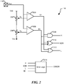
- FIG. 1 is a schematic diagram illustrating output driver circuitry 100 to detect a fault condition at a device interface according to a specific embodiment of the present disclosure.
- output driver circuitry 100 can be included at an application-specific integrated circuit (ASIC) or at another type of electronic device.
- the output driver circuitry 100 includes an output driver 110, ESD protection devices 112, an output terminal 114 coupled to an output load 119 via a bond wire 118, feedback circuit 116, and an error flag latch 120. Also illustrated are latches 102, 104, and 108, and logic 106 that are included to represent portions of a functional block that generates state information represented by signal BI.
- Output driver 110 is configured to propagate the state information to terminal 114.
- Feedback circuit 116 includes a first input to receive signal BI from the input of output driver 110, a second input to receive a signal V OUT present at output terminal 114, and an output to provide a signal labeled ERROR.
- Error latch 120 includes an input to capture the logic state of signal ERROR and an output to provide signal ERROR FLAG.
- Latches 102, 104, and 108 include a clock input terminal to receive a clock signal, CLK.
- Error flag latch 120 includes a clock input terminal that can be configured to receive clock signal CLK, however in the embodiment illustrated, the clock input terminal of error flag latch 120 receives a clock signal from delay circuit 122.
- Delay circuit 122 is configured to generate a delayed version of clock signal CLK, as described below.
- Latches 102, 104, 108, and error flag latch 120 are interconnected to provide a scan chain 124.
- Scan chain 124 provides a means to store and retrieve state information at each latch, including error information stored at error flag latch 120.
- Scan chain 124 includes an input labeled Scan_in, and an output labeled Scan_out.
- state information encoded by signal BI is provided to an input terminal of output driver 110.
- State information can be represented by a logic-high voltage signal or a logic-low voltage signal.
- output driver 110 is configured to communicate state information represented by signal BI to output terminal 114, also in the form of a logic-high voltage signal or a logic-low voltage signal.
- Output terminal 114 can be coupled to an input of another device, represented by output load capacitor 119 that is intended to receive the state information. Because a total capacitive load associated with terminal 114 and the receiving device can be greater than latch 108 is capable of driving, output driver 110 can include a buffer that provides greater drive capability.
- signal V OUT will represent the same state information represented by signal BI that is provided to the input of output driver 110. However, if there is a fault associated with output terminal 114, signal V OUT can be corrupted. For example, signal V OUT can be stuck at a logic-low level, stuck at a logic-high level, fail to fully transition to a legal logic level, or transition from one logic state to another logic state to quickly or too slowly. Feedback circuit 116 is configured to identify these corruptions.
- output driver 110 can be configured to provide a current-based interface, often referred to as an open-collector interface. During operation, output driver 110 converts state information represented by signal BI as described above into a corresponding sink current.
- a pull-up resistor or a transistor-based current source that can be included in the receiving device, is configured to elevate a voltage at terminal 114 unless countered by the sink current provided by output driver 110. For example, if signal BI is at a logic-low level, output driver 110 can be configured to sink a first amount of current, such as seven milliamps, and if signal BI is at a logic-high level, output driver 110 can be configured to sink a second amount of current, such as fourteen milliamps.
- the receiving device coupled to output terminal 114 can interpret the variation in sink current to represent the original state information represented by signal BI.
- feedback circuit 116 is configured to identify one or more fault conditions associated with output terminal 114. If a fault condition is identified, feedback circuit 116 can assert signal Error, which can subsequently be latched by error flag latch 120. In particular, feedback circuit 116 is configured to compare a voltage level of signal BI at the input of output driver 110 with a voltage level of signal V OUT at the output of output driver 110. The voltage level of signal V OUT is influenced by the characteristics of output driver 110 and of the external load 119. For example, output driver 110 can be damaged, preventing state information BI from being properly propagated to the external load. For another example, ESD protection devices 112 can be damaged, resulting in a short circuit of signal V OUT to the power or ground nodes.
- circuit failures include a break in bond wire 118 or an open or short circuit in conductors at the device receiving signal V OUT .
- Other circuit failures can result in the load impedance represented by external load 119 being too low or too high, which can result in kick-back noise, signal ringing, and the like.
- Feedback circuity 116 can include error logic which may be adapted by the designer for special needs of error detection to provide functional safety. Because error flag latch 120 is configured within scan chain 124, an error identified by feedback circuit 116 can be detected by internal built-in self test circuitry. Operation of feedback circuit 116 can be better understood with reference to FIG. 2 , below.
- FIG. 2 is a schematic diagram illustrating feedback circuit 116 of FIG. 1 according to a specific embodiment of the present disclosure.
- Feedback circuit 116 includes a variable resistor 202, a variable resistor 204, a voltage comparator 204, a voltage comparator 206, logic gates 208, 210, and 212, and error logic 216.
- Logic gate 208 provides an AND function
- logic gate 210 provides an XOR function
- logic gate 212 provides an OR function.
- Feedback circuit 116 receives signal V OUT from output terminal 114. Signal V OUT is connected to a non-inverting input of comparator 204 and to a non-inverting input of comparator 206.
- Variable resistors 202 and 204 are connected in series.
- variable resistor 202 A remaining terminal of variable resistor 202 is connected to a supply voltage reference, Vdd, and a remaining terminal of variable resistor 204 is connected to a ground voltage reference, Vss.
- a variable tap at resistor 202 is configured to provide a reference voltage V K to an inverting input of comparator 204
- a variable tap at resistor 204 is configured to provide a reference voltage V M to an inverting input of comparator 206.
- voltage references V K and V M can be generated by other means, such as using one or more digital to analog converters, a band-gap voltage reference, and the like.
- Comparator 204 has an output to generate signal K+, which is connected to a first input of logic gate 208, a first input of logic gate 210, and a first input of logic gate 212.
- comparator 206 has an output to generate signal M+, which is connected to a second input of logic gate 208, a second input of logic gate 210, and a second input of logic gate 212.
- Logic gate 208 has an output to generate a signal, H
- logic gate 210 has an output to generate a signal, XOR
- logic gate 212 has an output to generate signal, L.
- Error logic 216 includes a first input to receive signal H, a second input to receive signal XOR, a third input to receive signal L, a fourth input to receive signal BI, and an output to provide a signal, ERROR.
- signal M+ is asserted if a voltage level of signal V OUT exceeds threshold voltage V M and signal K+ is asserted if a voltage level of signal V OUT exceeds threshold voltage V K .
- reference voltages V M and V K can be selected so that signal K+ is asserted if signal V OUT represents a valid logic-high level, and M+ is not asserted if signal V OUT represents a valid logic-low level.
- Signal H is asserted if both signals K+ and M+ are asserted
- signal XOR is asserted only if signals K+ and M+ represent opposite logic states
- signal L is asserted if either signals K+ or M+ are asserted.
- Error logic 216 is configured to determine that a fault is associated with output terminal 114. For example, if signals H, L, and XOR are each at a logic-low level, this can be indicative of a short circuit between terminal 114 and a ground reference voltage. If signals H and L are each at a logic-high level and signal XOR is at a logic-low level, this can be indicative of a short circuit between terminal 114 and a supply reference voltage. Signal XOR is asserted if a voltage level of signal V OUT is between the levels of reference voltages V M and V K . Accordingly, if signal XOR is asserted, a duration (pulse width) of the assertion is representative of a transition time of signal V OUT .
- error logic 216 can determine whether the transition time of signal V OUT as indicated by signal XOR is less than a first predetermined value or greater than a second predetermined value. For example, if the transition time of signal V OUT is too fast, this can be indicative of an open circuit fault at terminal 114. If the transition time of signal V OUT is too slow, this can be indicative of excessive resistive or capacitive load at terminal 114.
- the duration of the assertion of signal XOR can be determined using a counter, and analog to digital converter, or another suitable technique.
- error logic 216 can determine a propagation delay of output driver 110, which can be indicative of a fault. For example, error logic 216 can measure a period of time between the assertion or de-assertion of signal BI and a corresponding assertion/de-assertion of signal V OUT .
- FIG. 3 is a timing diagram 300 illustrating the operation of feedback circuit 116 of FIGs. 1 and 2 according to a specific embodiment of the present disclosure.
- Timing diagram 300 includes a horizontal axis representing time and a vertical axis representing voltage.
- Timing diagram 300 further includes waveform 301 representing signal BI, waveform 302 representing signal V OUT ; threshold voltage M, 304; threshold voltage K, 306; signal H, 310; signal XOR, 312; signal L, 314; and time references 350, 351, 352, 353, and 354.
- Waveform 301 illustrates a transition of signal BI from a logic low level to a logic high level.
- signal V OUT (waveform 302) begins transitioning at time reference 351 and completes transitioning at time reference 354.
- a voltage level of signal V OUT has reached threshold voltage M 304; and at time reference 353, the voltage level of signal V OUT has reached threshold voltage K 306.
- the period of time from time reference 350 to time reference 352 can be referred to as the reaction delay of output driver 110, and the period of time from time reference 350 to time reference 353 can be referred to as the propagation delay of output driver 110.
- signal H is asserted by AND gate 208 at time reference 353 when a voltage level of signal V OUT exceeds threshold voltage K.
- Signal XOR is asserted at time reference 352 when the voltage level of signal V OUT exceeds threshold voltage M, and is de-asserted when the voltage level of signal V OUT further rises and exceeds threshold voltage K.
- Signal L is asserted when the voltage level of signal V OUT exceeds threshold voltage M.
- waveform 302 is illustrated as a piece-wise-linear form, waveform 302 is like exponential in shape as would be expected when driving a load having resistance and capacitance characteristics.
- output driver 110 and signal VOUT are described in the context of a digital logic interface, one of skill will be appreciated that compare logic 116 and the concepts described above can be applied to an analog interface.
- error logic 216 can assert signal ERROR if a fault associated with output terminal 114 is detected.
- signal ERROR can be latched by error flag latch 120 of FIG. 1 .
- a delay provided by delay circuit 122 can be adjusted to control when signal ERROR is latched at error flag latch 120.
- delay circuit 122 can include selectable buffer delays, a delay-locked-loop, and the like, to delay the generation of signal CLK_D relative to signal CLK.
- a digital data processing device such as an ASIC device, can include a clock circuit to generate one or more internal clock signals.
- latch 108 includes an input to receive a clock signal, CLK, which controls the timing of signal BI.
- Output driver 110 and feedback circuit 116 each introduce delay.
- Signal ERROR is captured by latch 120 based on the delayed clock signal CLK_D. Accordingly, the propagation delay of signal V OUT relative to signal BI (and clock signal CLK) can be measured by adjusting the delay of clock signal CLK_D.
- FIG. 4 is a schematic diagram illustrating an output driver circuit 400 to detect a fault condition at a device interface that operates in a current domain, according to a specific aspect of the present disclosure. Similar to output driver circuit 100 of FIG. 1 , output driver circuit 400 is configured to communicate information from an electronic device, which includes output driver circuit 400, to another device. The information is encoded using two or more discrete current sink values. For example, a first logic state can be represented by one particular sink current, while another logic state can be represented by a different sink current. A current is received at an output terminal 441 from a source that is external to driver circuit 400.
- a current source can be provided by a pull-up resistor or transistor circuit included at the receiving device, or pull-up circuitry external to both the transmitting and receiving devices.
- Output driver circuit 400 is configured to selectively sink predefined current values corresponding to each of two or more logic states.
- the selective sink current and external current source together, form a voltage divider. Accordingly, a voltage, V OUT , at an output terminal 441 will vary depending on the amount of current sunk by output driver circuit 400.
- the sink current is labeled, I OUT , at FIG. 4 .
- Output driver circuit 400 includes transistors 401, 402, 403, 404, 405, 406, 407, 408, 409, 411, 412, 413, 414, 416, 417, 432, 433, 434, 436, and 437; resistors 421, 422, 425, and 426; capacitors 423, 424, and 427; a current source 410; a diode 444; inverters 451 and 452; and the output terminal 441.
- the external current source and receiving device are represented by resistor 443, Rload, and parasitic capacitor 442, which are coupled to output driver circuit 400 via a bond wire 444 to output terminal 441.
- Resistor 443 and parasitic capacitor 442 are coupled to a power supply Vext, indicated by the diagonal supply symbol, that is associated with the device receiving information from output driver circuitry 100.
- Output driver circuit 400 is best described by partitioning the circuit into functional blocks.
- the functional blocks include a high voltage output circuit 481, a current sink mirror 482, a feedback current mirror 483, a reference current circuit 484, a current level switch 485, and a current comparator 486, which are described below.
- Circuit 400 provides a current path 480 from the output terminal 441 to a ground reference voltage, Vss.
- Current path 480 conducts the selected sink current, I OUT , and includes a series connection of current electrodes of transistors 405, 402, and 404.
- current electrodes of a transistor include drain/source terminals of a field-effect transistor, collector/emitter terminals of a bipolar transistor, and the like.
- a gate or base terminal of a transistor is herein referred to as a control electrode.
- a voltage at the control electrode of transistor 402 determines how much current is permitted to flow in current path 480.
- the control electrode of transistor 402 is used to selectively control the magnitude of a sink current provided at output terminal 441.
- High voltage output circuit 481 includes output terminal 441, transistor 405, diode 444, capacitor 442, and resistor 443.
- Diode 444 represents an electrostatic discharge protection circuit.
- Output driver circuit 400 can support communication with a receiving device that operates at a supply voltage, Vext, that is greater than a supply voltage, Vdd, of the transmitting device that includes driver circuit 400.
- transistor 405 is a high voltage transistor configured to isolate transistors 402 and 404 from Vext.
- the drain of transistor 405 is fabricated to withstand the maximum specified external supply voltage Vext.
- control electrode of transistor 405 is coupled to a supply voltage, Vcas, that is greater than the supply voltage Vdd so that transistor 405 does not further limit the amount of current that can flow at current path 480.
- Supply voltage Vcas can be generated using a charge pump based on supply voltage Vdd.
- Reference current circuit 484 includes current source 410 and transistor 411.
- Current source 410 provides a reference current, Ir, to a current electrode and a control electrode of transistor 411.
- Current source 410 can be external or internal to output driver 400, and can be provided by a bandgap circuit, or another type of current source.
- current source 410 provides a small but highly accurate current, and can include features to support trimming the value of reference current Ir.
- a current value provided by current source 410 can be regulated or calibrated using laser-trimming at the die level, fuse programming, programmable digital to analog converter circuitry, and the like.
- Transistor 411 is configured as a source device of a plurality of current mirrors.
- Transistor 412, 413, 414, 416, and 417 are each configured to mirror reference current Ir.
- a current mirror is a circuit configuration where a transistor is biased to conduct an amount of current that is proportional to a current conducted in another transistor.
- the phrase mirroring a current conducted at a first transistor at a second transistor is intended to mean that the second transistor is biased to conduct a maximum current that is proportional to a current conducted at the first transistor.
- the actual current conducted at the second transistor may be less than the maximum value.
- each current mirror can be configured to provide gain, wherein the mirrored current is an integer or non-integer multiple of the reference current Ir.
- Capacitor 427 is a fabricated capacitor to stabilize operation of the current mirror.
- capacitor 427 can be a gate-oxide capacitor, a metal plate capacitor, and the like.
- Current level switch 485 includes transistor 412, 413, 414, 432, 433, and 434.
- Control electrodes of each of transistors 412, 413, and 414 are connected to the control electrode of transistor 411 so that a current at the drain terminals of each of transistors 412, 413, and 414 provides a current that mirrors reference current Ir.
- the effective width of transistors 412, 413, and 414 are configured to provide specific currents, IrH, IrL, and IrS, that are each a multiple of reference current Ir.
- the effective width of transistor 412 can be three times the effective width of transistor 411 so that a value of current IrS is three times the value of reference current Ir; the effective width of transistor 413 can be seven times the effective width of transistor 411 so that a value of current IrL is seven times the value of reference current Ir; and the effective width of transistor 414 can be fourteen times the effective width of transistor 411 so that a value of current IrH is fourteen times the value of reference current Ir.
- the current level switch can include as few as two mirror devices, or can include greater than three mirror devices.
- the effective width of a transistor refers to the total current carrying capacity of the transistor, or plurality of transistors, when activated.
- the current carrying capacity of a transistor is determined based on a width and length of a channel formed when the transistor is activated.
- an effective width of a transistor can be provided by fabricating a single transistor with a desired channel width, or by providing two or more transistor that provide a parallel path for current to travel.
- an effective width of ten microns can be provided by a single transistor have a channel width of ten microns, by two transistors having a channel width of approximately five microns that are connected in parallel, and the like.
- Transistors 432, 433, and 434 are configured as switches that can be activated by signals Sw_S, Sw_L, and Sw_H, respectively. During operation, one or more of transistors 432, 433, and 434 can be activated by asserting a corresponding one or more of signals Sw_S, Sw_L, and Sw_H to adjust a value of output current IrO that is generated by the current level switch. For example, based on the exemplary values described above, asserting signals Sw_S and Sw_L simultaneously would result in output current IrO having a value equal to the sum of currents IrS (3 x Ir) and IrL (7 x Ir), or ten times the value of reference current Ir.
- switches Sw_S, Sw_L, and Sw_H are activated and deactivated to control a sink current provided by output driver 400 at output terminal 441, the activation and deactivation determined based on state information being transmitted to the receiving device. For example, a logic-high state may correspond to a sink current corresponding to the assertion of signal Sw_H and a logic-low state may correspond to a sink current corresponding to the assertion of signal Sw_L.
- a logic-high state may correspond to a sink current corresponding to the assertion of signal Sw_H and signal Sw_L
- a logic-low state may correspond to a sink current corresponding to the assertion of signal Sw_L
- switch configurations that provide discrete values of sink current at output terminal 441 that correspond to logic respective state values.
- Current sink mirror 482 includes transistor 401 and transistor 402.
- the control electrode of transistor 401 is connected to the control electrode of transistor 402, and this circuit node is labeled Vr.
- current IrO selected by the current level switch 485 and conducted by transistor 401 is mirrored by transistor 402.
- the effective width of transistor 402 is greater than the effective width of transistor 401 so that the mirrored current conducted by transistor 402 is an integer or non-integer multiple of current IrO.
- the ratio of the effective width of transistor 402 to the effective width of transistor 401, and accordingly the current gain provided by the current sink mirror, will be referred to herein as current gain J.
- transistor 402 is configured to conduct a current equal to J x IrO.
- a current gain of ten can be provided by selecting an effective width of transistor 402 that is ten times the effective width of transistor 401.
- Providing gain at current sink mirror 482 reduces current consumption and associated power dissipation of current level switch 485, current comparator 486, and reference current circuit 484.
- the current gain J can be a fixed value by design.
- transistor 402 can be replaced with multiple output transistors and the gain J can be made adjustable by switches operable to select one or more of the output transistors.
- Capacitor 424 is a fabricated capacitor to stabilize operation of current sink mirror 482.
- capacitor 424 can be a gate-oxide capacitor, a metal plate capacitor, and the like
- current, I OUT conducted by current path 480 provided by transistors 402, 404, and 405 is J x IrO, where current IrO is adjusted by the current level switch.
- current I OUT can be different than the desired value, J x IrO.
- an open circuit fault isolates output terminal 441 from the external pullup current source, e.g. if bond wire 444 is broken, Rload, current I OUT will be zero.
- Other faults can result in current I OUT being less than the desired value, J x IrO. Fault detection is described below in greater detail.
- Feedback current mirror 483 is configured to monitor the actual current being conducted in current path 480.
- Feedback current mirror 483 includes transistor 404 and transistor 403, which together provide another current mirror.
- the control electrode of transistor 404 is connected to the control electrode of transistor 403, and this circuit node is labeled Vf.
- transistor 403 is configured to mirror a current conducted at transistor 404.
- this feedback current mirror is configured to provide a current gain of 1/J.
- the effective width of transistor 404 can be ten times the effective width of transistor 403.
- the effective width of transistor 404 can be the same as the effective width of transistor 402, and the effective width of transistor 403 can be the same as the effective width of transistor 401.
- Feedback current mirror 483 measures the actual current conducted at current path 480 and mirrors it back, by a current gain of 1/J, to current comparator 486. It is desired that feedback current mirror follow output current I OUT quickly, so parasitic gate capacitance 423 should be small. It is further desired that transistor 403 does not limit current IrO significantly.
- Resistors 421 and 422 are selected to provide a voltage drop of approximately one hundred millivolts. Accordingly, a resistance provided by resistor 421 is approximately one tenth the resistance provided by resistor 422.
- Current comparator 486 is configured to compare the actual current I OUT conducted at current path 480 with the intended value, IrO x J.
- Current comparator 486 includes transistors 416, 417, 437, 437, 406, 407, 408, and 409.
- Current comparator 486 includes two controllable reference currents, IrM and IrK, which define current thresholds.
- Current comparator 486 is configured to compare current I OUT /J (current I OUT divided by current gain J) with each reference current.
- Transistors 416 and 417 can represent two or more current mirror transistors that mirror reference current Ir.
- Transistors 436 and 437 can represent two or more switch transistors that are controlled to select corresponding current mirror transistors so as to provide the desired values of references currents IrM and IrK.
- transistor 416, 417, 436, and 437 provide a current-based digital-to-analog converter that is similar to current level switch 485.
- Control electrodes of transistors 406 and 407 are connected to node Vr and thus implement current mirrors, which mirror current IrO conducted by transistor 401.
- the effective width of transistors 406 and 407 can be the same as the effective width of transistor 401.
- Control electrodes of transistors 408 and 409 are connected to node Vf and thus implement current mirrors, which mirror current I OUT conducted by transistor 404.
- the effective width of transistors 408 and 409 can be the same as the effective width of transistor 403, and the impedance of resistor 425 and resistor 426 can be the same as the impedance of resistor 422.
- a voltage at node A will correspond to a logic-low state if output current I OUT /J is greater than current IrM
- node B will correspond to a logic-low state if current I OUT /J is greater than current IrK.
- Inverters 452 and 451 invert the logic state at nodes A and B, respectively. Accordingly, output M+ will be asserted with a logic high level if output current I OUT /J is greater than current IrM, and output K+ will be asserted with a logic high level if output current I OUT /J is greater than current IrK.
- a current threshold represented by current IrM can be selected to correspond to a value equal to ten percent of a maximum value of output current I OUT /J
- a current threshold represented by current IrK can be selected to correspond to a value equal to ninety percent of a maximum value of output current I OUT /J.
- FIG. 5 is a schematic diagram illustrating fault detection logic 500 according to a specific embodiment of the present disclosure.
- Fault detection logic 500 includes logic gates 508, 510, 512, and error logic 516. Operation of fault detection logic 500 is similar to operation of portions of feedback logic of FIG. 2 .
- Fault detection logic 500 receives signals K+ and M+ from current comparator 486 of FIG. 4 and signal BI, and generates signal ERROR.
- Logic gates 508, 510, and 512 each have inputs to receive signals K+ and M+, and outputs to generate signals H, XOR, and L, respectively.
- Error logic 516 includes a first input to receive signal H, a second input to receive signal XOR, a third input to receive signal L, a fourth input to receive signal BI, and an output to provide a signal, ERROR.
- Signal BI represents an intended current sink value, as encoded by signal Sw_H, Sw_L, and Sw_S.
- error logic 516 can determine whether the transition time of signal I OUT /J as indicated by signal XOR is less than a first predetermined value or greater than a second predetermined value.
- Fault detection logic 500 is configured to detect a fault associated with output terminal 441.
- output current I OUT will be zero, and signals H, L, and XOR will each be at a logic-low level. If output driver circuit 400 is configured to sink a high current level, but a fault causes output current I OUT /J to be less than a corresponding high current level represented by current IrK, signal H will not be asserted. If output terminal is shorted to external voltage Vext, the duration of an assertion of signal XOR will be less than expected, because the time constant associated with capacitor 442 and resistor 443 will be nearly zero.
- FIG. 6 is a timing diagram 600 illustrating the operation of the output driver circuit 400 of FIG. 4 and fault detection logic 500 of FIG. 5 according to a specific embodiment of the present disclosure.
- Timing diagram 600 includes a horizontal axis representing time and a vertical axis representing current.
- Timing diagram 600 further includes waveform 602 representing current I OUT /J; threshold current IrM, 604; threshold current IrK, 606; signal H, 610; signal XOR, 612; signal L, 614; and time references 650, 652, 654, and 656.
- Waveform 602 illustrates a transition of current I OUT /J from a current level representing logic low level, such as IrL, to a current representing a logic high level, such as IrH.
- Waveform 602 begins transitioning at time reference 650 and completes transitioning at time reference 656.
- current I OUT /J has reached threshold current IrM, 604; and at time reference 654, current I OUT /J has reached threshold current IrK, 606.
- signal H is asserted by AND gate 508 at time reference 654 when current I OUT /J exceeds threshold current IrK.
- Signal XOR is asserted at time reference 652 when current I OUT /J exceeds threshold current IrM, and is de-asserted when the current I OUT /J further rises and exceeds threshold current IrK.
- Signal L is asserted when current I OUT /J exceeds threshold current IrM.
- waveform 602 is illustrated as a piece-wise-linear form, waveform 602 is likely exponential in shape as would be expected when driving a load having resistance and capacitance characteristics.
- output driver 400 and signals V OUT and I OUT are described in the context of a digital logic interface, one of skill will appreciated that fault detection logic 500 and the concepts described above can be applied to an analog current interface.
- FIG. 7 is a schematic diagram illustrating an output driver circuit 700 to detect a fault condition at a device interface that operates in a current domain, according to another aspect of the present disclosure.
- Output driver circuit 700 is substantially similar to output driver circuit 400 with one exception.
- Each reference number, 7xx, of FIG. 7 corresponds to the similarly numbered references, 4xx, of FIG. 4 .
- capacitor 442 of FIG. 4 corresponds to capacitor 742 of FIG. 7 .
- the operation of the functional blocks of output driver circuit 700 is substantially the same as the operation of the functional blocks of output driver circuit 400. Accordingly, reference numbers of FIG. 7 that do not appear below correspond to elements of FIG. 4 that function substantially the same as described above with reference to FIG. 4 .
- circuit 700 The difference between circuit 700 and circuit 400 is the configuration of the current sink mirror 782 and feedback current mirror 783. Specifically, the series connected order of transistors 704 and 702 of a current path 780 are switched relative to the series connected order of transistors 402 and 404 of current path 480 of FIG. 4 . The series connected order of transistors 703 and 701 are similarly reversed relative to transistor 401 and 403.
- Output driver circuit 400 uses a Wilson current mirror that generates a voltage drop of greater than two threshold voltages of transistor 401 and transistor 403. Accordingly, output driver circuit 400 requires a supply voltage that is greater than approximately 1.8v for some integrated circuit process technologies. Instead, output driver circuit 700 uses a cascode current mirror that generates a voltage drop that is less than that of circuit 400. Therefore, circuit 700 can operate using a supply voltage that is lower than that required by circuit 400, for a particular process technology.
- Current sink mirror 782 includes transistor 701 and transistor 702.
- the control electrode of transistor 701 is connected to the control electrode of transistor 702, and this circuit node is labeled Vr.
- current IrO selected by current level switch 785 and conducted by transistor 701 is mirrored by transistor 702.
- the effective width of transistor 702 is greater than the effective width of transistor 701 so that the mirrored current conducted by transistor 702 is an integer or non-integer multiple of current IrO.
- the ratio of the effective width of transistor 702 to the effective width of transistor 701, and accordingly the current gain provided by current sink mirror 782, will be referred to herein as current gain J.
- transistor 702 is configured to conduct a current equal to J x IrO.
- Capacitor 724 is a fabricated capacitor to stabilize operation of current sink mirror 782.
- capacitor 724 can be a gate-oxide capacitor, a metal plate capacitor, and the like
- Feedback current mirror 783 is configured to monitor the actual current being conducted in current path 780.
- Feedback current mirror 783 includes transistor 704 and transistor 703, which together provide another current mirror.
- the control electrode of transistor 704 is connected to the control electrode of transistor 703, and this circuit node is labeled Vf.
- transistor 703 is configured to mirror a current conducted at transistor 704.
- Transistor 703 is in a cascode configuration.
- this feedback current mirror is configured to provide a current gain of 1/J.
- the effective width of transistor 704 can be J times the effective width of transistors 706 and 707 of current comparator 786.
- the effective width of transistor 704 can be the same as the effective width of transistor 702, and the effective width of transistor 703 can be the same as the effective width of transistor 701.
- resistor 721 is selected to provide a voltage drop of approximately one hundred millivolts. Accordingly, a resistance provided by resistor 721 should be approximately one tenth the resistance provided by resistor 722.
- a device in a first aspect, includes an output terminal and a first current path from the output terminal to a first reference voltage.
- the first current path includes a series connection of current electrodes of a first transistor and a second transistor.
- the first transistor receives at a control electrode a signal to set a desired level of current to be conducted by the first current path.
- the second transistor generates at a control electrode a feedback signal indicative of an actual current conducted by the first transistor.
- the device further includes a third transistor that together with the first transistor provides a first current mirror.
- the device further includes a first reference current source to provide a first reference current; and a second current mirror to generate a second reference current based on the first reference current, the second current mirror coupled to a first current electrode and to a control electrode of the third transistor.
- the device further includes a third transistor that together with the second transistor provides a second current mirror.
- the device further includes a current comparator to compare the actual current conducted by the first transistor, as indicated by the feedback signal, to a first threshold current and to a second threshold current.
- the device further includes control logic coupled to the current comparator, the control logic to assert a first indicator if the actual current is greater than the first threshold current; assert a second indicator if the actual current is greater than the second threshold current; and assert a third indicator if the actual current is greater than the first threshold current and less than the second threshold current.
- the duration of the assertion of the third indicator corresponds to a transition time of a voltage at the output terminal.
- a method in a second aspect, includes receiving a control current at a current electrode of a first transistor of a first current mirror, wherein current electrodes of a second transistor of the current mirror are included in a first current path, the first current path for selectively sinking current at an output terminal; and generating a feedback signal at a control electrode of a third transistor, current electrodes of the third transistor included in the first current path, the feedback signal indicating an actual current conducted by the second transistor.
- the method includes mirroring a current conducted at the third transistor at a fourth transistor, a current electrode of the fourth transistor coupled to a current electrode of the first transistor.
- the method includes generating the control current at a second current mirror, the control current a mirror of a reference current.
- the method includes mirroring a current conducted at the first transistor at a fourth transistor and a fifth transistor of a current comparator; and mirroring a current conducted at the third transistor at a sixth transistor and a seventh transistor of the current comparator.
- the method includes generating a first threshold current and a second threshold current; and providing the first threshold current and the second threshold current to the current comparator.
- the method includes generating a first output signal at the current comparator, the first output signal, if asserted, indicating that the actual current is greater than the first threshold current; and generating a second output signal at the current comparator, the second output signal, if asserted, indicating that the actual current is greater than the second threshold current.
- the method includes determining that there is a defective component or a defect in connectivity of components associated with the output terminal and the first current path based on first output signal and the second output signal.
- an integrated circuit in a third aspect, includes an output terminal; a first current path includes current electrodes of a first transistor and current electrodes of a second transistor; a third transistor, a control electrode of the third transistor connected to a control electrode of the first transistor and to a first current electrode of the third transistor; a fourth transistor, a control electrode of the fourth transistor connected to a control electrode of the second transistor, the control electrode of the second transistor connected to a first current electrode of the second transistor.
- the integrated circuit includes a fifth transistor to provide a first current to the first current electrode of the third transistor.
- the integrated circuit includes a current comparator.
- the current comparator includes a fifth transistor to provide a first threshold current; a sixth transistor, a current electrode of the sixth transistor coupled to a current electrode of the fifth transistor, and a control electrode of the sixth transistor connected to the control electrode of the first transistor; and a seventh transistor, a current electrode of the seventh transistor coupled to a current electrode of the sixth transistor and a control electrode of the seventh transistor connected to the control electrode of the second transistor.
- the current comparator further includes an eighth transistor to provide a second threshold current; a ninth transistor, a current electrode of the ninth transistor coupled to a current electrode of the eighth transistor, and a control electrode of the ninth transistor connected to the control electrode of the first transistor; and a tenth transistor, a current electrode of the tenth transistor coupled to a current electrode of the eighth transistor and a control electrode of the tenth transistor connected to the control electrode of the second transistor.
- the current comparator further includes a first comparator output coupled to the current electrode of the sixth transistor, assertion of the first comparator output to indicate that a current conducted at the first current path exceeds the first threshold current; and a second comparator output coupled to the current electrode of the ninth transistor, assertion of the second comparator output to indicate that the current conducted at the first current path exceeds the second threshold current.
- the first current path further includes current electrodes of a fifth transistor, a first current electrode of the fifth transistor connected to the output terminal, and a control electrode of the fifth transistor coupled to an internal supply voltage, the fifth transistor to isolate the first transistor from an external supply voltage.
Abstract
Description
- This disclosure relates generally to integrated circuits, and more particularly to identifying a fault at a device output.
- An electronic system can include multiple devices, such as integrated circuits. An electronic device can include circuitry to interface with another device. For example, an integrated circuit can include an output terminal and an associated output driver for transmitting information to another integrated circuit. The information can be encoded and transmitted using a voltage or a current signal. For example, an output driver can include push-pull circuitry to provide a signal where the information to be transmitted is encoded using discrete voltage levels corresponding to a logic-high or a logic-low state. Alternatively, an output driver can selectively enabled to sink current provided by external pull-up circuitry, where particular levels of the sink current corresponding to individual logic states. Furthermore, an output driver can provide an analog interface, in which case the output driver provides a continuously range of voltage or current instead of discrete levels. Many failures that can occur within an electronic device can be detected using testing protocols and associated test circuitry. For example, the logic state of latch devices can be evaluated using test-scan technology. Other forms of built-in self-test can validate the operation of a functional block by providing diagnostic stimulus and evaluating how the functional block responds to the stimulus. Faults associated with output drive circuits can be difficult to identify, especially while the electronic system is functioning in its normal operating mode. Faults associated with an output driver can include defective transistors in the driver circuit, broken or shorted bonding wires, damaged cables or connectors that couple the output signal to the receiving device, failed electrostatic-discharge protection components, defective printed circuit board conductors, and the like. Undetected faults can have serious implications. For example, a fault in an automotive emergency braking system can result in a collision.
- According to the invention there is provided a device as claimed in claim 1 and a method as claimed in claim 7. Optional features are defined in the dependent claims.
- The present disclosure may be better understood, and its numerous features and advantages made apparent to those skilled in the art by referencing the accompanying drawings.
-
FIG. 1 is a schematic diagram illustrating output driver circuitry to detect a fault condition at a device interface according to a specific embodiment of the present disclosure. -
FIG. 2 is a schematic diagram illustrating feedback logic ofFIG. 1 according to a specific embodiment of the present disclosure. -
FIG. 3 is a timing diagram illustrating the operation of feedback circuit ofFIGs. 1 and2 according to a specific embodiment of the present disclosure. -
FIG. 4 is a schematic diagram illustrating an output driver circuit to detect a fault condition at a device interface that operates in a current domain, according to a specific aspect of the present disclosure. -
FIG. 5 is a schematic diagram illustrating fault detection logic according to a specific embodiment of the present disclosure. -
FIG. 6 is a timing diagram illustrating the operation of the output driver circuit ofFIG. 4 and fault detection logic ofFIG. 5 according to a specific embodiment of the present disclosure. -
FIG. 7 is a schematic diagram illustrating an output driver circuit to detect a fault condition at a device interface that operates in a current domain, according to another aspect of the present disclosure. - The use of the same reference symbols in different drawings indicates similar or identical items.
-
FIGs. 1-7 illustrate techniques for detecting a fault condition at an output driver of an electronic system. Faults can include open circuit conditions and short circuit conditions. For example, a bond wire used to connect a terminal of an integrated circuit (IC) die to a corresponding IC package can fail, typically resulting in an open circuit condition. IC interfaces typically include electrostatic-discharge (ESD) devices that can fail creating a short circuit to a power or ground supply rail. In an automotive environment, the driving and receiving devices are likely coupled using cables and one or more electrical connectors, where a fault usually results in an open circuit condition. Techniques disclosed herein provide a feedback signal at an output driver that can be used to detect open circuit and short circuit faults, as well as faults that cause other anomalous load characteristics. For example, the feedback signal can monitor the transition time of an output signal and determine if the transition time is faster or slower than expected. The disclosed techniques can be utilized for either voltage or current based interfaces. While the techniques are described in the context of an interface between individual integrated circuits, the techniques can be utilized at any functional boundary, such as the interface of intellectual property (IP) blocks included at a system on chip (SOC) device. -
FIG. 1 is a schematic diagram illustratingoutput driver circuitry 100 to detect a fault condition at a device interface according to a specific embodiment of the present disclosure. For example,output driver circuitry 100 can be included at an application-specific integrated circuit (ASIC) or at another type of electronic device. Theoutput driver circuitry 100 includes anoutput driver 110,ESD protection devices 112, anoutput terminal 114 coupled to anoutput load 119 via abond wire 118,feedback circuit 116, and anerror flag latch 120. Also illustrated arelatches logic 106 that are included to represent portions of a functional block that generates state information represented by signal BI.Output driver 110 is configured to propagate the state information toterminal 114.Feedback circuit 116 includes a first input to receive signal BI from the input ofoutput driver 110, a second input to receive a signal VOUT present atoutput terminal 114, and an output to provide a signal labeled ERROR.Error latch 120 includes an input to capture the logic state of signal ERROR and an output to provide signal ERROR FLAG. -
Latches Error flag latch 120 includes a clock input terminal that can be configured to receive clock signal CLK, however in the embodiment illustrated, the clock input terminal oferror flag latch 120 receives a clock signal fromdelay circuit 122.Delay circuit 122 is configured to generate a delayed version of clock signal CLK, as described below.Latches error flag latch 120 are interconnected to provide ascan chain 124.Scan chain 124 provides a means to store and retrieve state information at each latch, including error information stored aterror flag latch 120.Scan chain 124 includes an input labeled Scan_in, and an output labeled Scan_out. - During operation, state information encoded by signal BI is provided to an input terminal of
output driver 110. State information can be represented by a logic-high voltage signal or a logic-low voltage signal. In an embodiment,output driver 110 is configured to communicate state information represented by signal BI tooutput terminal 114, also in the form of a logic-high voltage signal or a logic-low voltage signal.Output terminal 114 can be coupled to an input of another device, represented byoutput load capacitor 119 that is intended to receive the state information. Because a total capacitive load associated withterminal 114 and the receiving device can be greater thanlatch 108 is capable of driving,output driver 110 can include a buffer that provides greater drive capability. If there is not a fault associated withoutput terminal 114, signal VOUT will represent the same state information represented by signal BI that is provided to the input ofoutput driver 110. However, if there is a fault associated withoutput terminal 114, signal VOUT can be corrupted. For example, signal VOUT can be stuck at a logic-low level, stuck at a logic-high level, fail to fully transition to a legal logic level, or transition from one logic state to another logic state to quickly or too slowly.Feedback circuit 116 is configured to identify these corruptions. - In another embodiment,
output driver 110 can be configured to provide a current-based interface, often referred to as an open-collector interface. During operation,output driver 110 converts state information represented by signal BI as described above into a corresponding sink current. A pull-up resistor or a transistor-based current source, that can be included in the receiving device, is configured to elevate a voltage atterminal 114 unless countered by the sink current provided byoutput driver 110. For example, if signal BI is at a logic-low level,output driver 110 can be configured to sink a first amount of current, such as seven milliamps, and if signal BI is at a logic-high level,output driver 110 can be configured to sink a second amount of current, such as fourteen milliamps. The receiving device coupled tooutput terminal 114 can interpret the variation in sink current to represent the original state information represented by signal BI. - During operation,
feedback circuit 116 is configured to identify one or more fault conditions associated withoutput terminal 114. If a fault condition is identified,feedback circuit 116 can assert signal Error, which can subsequently be latched byerror flag latch 120. In particular,feedback circuit 116 is configured to compare a voltage level of signal BI at the input ofoutput driver 110 with a voltage level of signal VOUT at the output ofoutput driver 110. The voltage level of signal VOUT is influenced by the characteristics ofoutput driver 110 and of theexternal load 119. For example,output driver 110 can be damaged, preventing state information BI from being properly propagated to the external load. For another example,ESD protection devices 112 can be damaged, resulting in a short circuit of signal VOUT to the power or ground nodes. Other circuit failures include a break inbond wire 118 or an open or short circuit in conductors at the device receiving signal VOUT. Other circuit failures can result in the load impedance represented byexternal load 119 being too low or too high, which can result in kick-back noise, signal ringing, and the like.Feedback circuity 116 can include error logic which may be adapted by the designer for special needs of error detection to provide functional safety. Becauseerror flag latch 120 is configured withinscan chain 124, an error identified byfeedback circuit 116 can be detected by internal built-in self test circuitry. Operation offeedback circuit 116 can be better understood with reference toFIG. 2 , below. -
FIG. 2 is a schematic diagram illustratingfeedback circuit 116 ofFIG. 1 according to a specific embodiment of the present disclosure.Feedback circuit 116 includes avariable resistor 202, avariable resistor 204, avoltage comparator 204, avoltage comparator 206,logic gates error logic 216.Logic gate 208 provides an AND function,logic gate 210 provides an XOR function, andlogic gate 212 provides an OR function.Feedback circuit 116 receives signal VOUT fromoutput terminal 114. Signal VOUT is connected to a non-inverting input ofcomparator 204 and to a non-inverting input ofcomparator 206.Variable resistors variable resistor 202 is connected to a supply voltage reference, Vdd, and a remaining terminal ofvariable resistor 204 is connected to a ground voltage reference, Vss. A variable tap atresistor 202 is configured to provide a reference voltage VK to an inverting input ofcomparator 204, and a variable tap atresistor 204 is configured to provide a reference voltage VM to an inverting input ofcomparator 206. One of skill will appreciate that whilevariable resistors -
Comparator 204 has an output to generate signal K+, which is connected to a first input oflogic gate 208, a first input oflogic gate 210, and a first input oflogic gate 212. Similarly,comparator 206 has an output to generate signal M+, which is connected to a second input oflogic gate 208, a second input oflogic gate 210, and a second input oflogic gate 212.Logic gate 208 has an output to generate a signal, H,logic gate 210 has an output to generate a signal, XOR, andlogic gate 212 has an output to generate signal,L. Error logic 216 includes a first input to receive signal H, a second input to receive signal XOR, a third input to receive signal L, a fourth input to receive signal BI, and an output to provide a signal, ERROR. - During operation, signal M+ is asserted if a voltage level of signal VOUT exceeds threshold voltage VM and signal K+ is asserted if a voltage level of signal VOUT exceeds threshold voltage VK. For example, reference voltages VM and VK can be selected so that signal K+ is asserted if signal VOUT represents a valid logic-high level, and M+ is not asserted if signal VOUT represents a valid logic-low level. Signal H is asserted if both signals K+ and M+ are asserted, signal XOR is asserted only if signals K+ and M+ represent opposite logic states, and signal L is asserted if either signals K+ or M+ are asserted.
-
Error logic 216 is configured to determine that a fault is associated withoutput terminal 114. For example, if signals H, L, and XOR are each at a logic-low level, this can be indicative of a short circuit betweenterminal 114 and a ground reference voltage. If signals H and L are each at a logic-high level and signal XOR is at a logic-low level, this can be indicative of a short circuit betweenterminal 114 and a supply reference voltage. Signal XOR is asserted if a voltage level of signal VOUT is between the levels of reference voltages VM and VK. Accordingly, if signal XOR is asserted, a duration (pulse width) of the assertion is representative of a transition time of signal VOUT. In an embodiment,error logic 216 can determine whether the transition time of signal VOUT as indicated by signal XOR is less than a first predetermined value or greater than a second predetermined value. For example, if the transition time of signal VOUT is too fast, this can be indicative of an open circuit fault atterminal 114. If the transition time of signal VOUT is too slow, this can be indicative of excessive resistive or capacitive load atterminal 114. The duration of the assertion of signal XOR can be determined using a counter, and analog to digital converter, or another suitable technique. In an embodiment,error logic 216 can determine a propagation delay ofoutput driver 110, which can be indicative of a fault. For example,error logic 216 can measure a period of time between the assertion or de-assertion of signal BI and a corresponding assertion/de-assertion of signal VOUT. -
FIG. 3 is a timing diagram 300 illustrating the operation offeedback circuit 116 ofFIGs. 1 and2 according to a specific embodiment of the present disclosure. Timing diagram 300 includes a horizontal axis representing time and a vertical axis representing voltage. Timing diagram 300 further includeswaveform 301 representing signal BI,waveform 302 representing signal VOUT; threshold voltage M, 304; threshold voltage K, 306; signal H, 310; signal XOR, 312; signal L, 314; and time references 350, 351, 352, 353, and 354.Waveform 301 illustrates a transition of signal BI from a logic low level to a logic high level. In response to the transition of signal BI, signal VOUT (waveform 302) begins transitioning attime reference 351 and completes transitioning attime reference 354. Attime reference 352, a voltage level of signal VOUT has reachedthreshold voltage M 304; and attime reference 353, the voltage level of signal VOUT has reachedthreshold voltage K 306. The period of time fromtime reference 350 totime reference 352 can be referred to as the reaction delay ofoutput driver 110, and the period of time fromtime reference 350 totime reference 353 can be referred to as the propagation delay ofoutput driver 110. As described above, signal H is asserted by ANDgate 208 attime reference 353 when a voltage level of signal VOUT exceeds threshold voltage K. Signal XOR is asserted attime reference 352 when the voltage level of signal VOUT exceeds threshold voltage M, and is de-asserted when the voltage level of signal VOUT further rises and exceeds threshold voltage K. Signal L is asserted when the voltage level of signal VOUT exceeds threshold voltage M. One of skill will appreciate that whilewaveform 302 is illustrated as a piece-wise-linear form,waveform 302 is like exponential in shape as would be expected when driving a load having resistance and capacitance characteristics. Furthermore, whileoutput driver 110 and signal VOUT are described in the context of a digital logic interface, one of skill will be appreciated that comparelogic 116 and the concepts described above can be applied to an analog interface. - Returning to
FIG. 2 ,error logic 216 can assert signal ERROR if a fault associated withoutput terminal 114 is detected. As described above, signal ERROR can be latched byerror flag latch 120 ofFIG. 1 . In an embodiment, a delay provided bydelay circuit 122 can be adjusted to control when signal ERROR is latched aterror flag latch 120. For example,delay circuit 122 can include selectable buffer delays, a delay-locked-loop, and the like, to delay the generation of signal CLK_D relative to signal CLK. A digital data processing device, such as an ASIC device, can include a clock circuit to generate one or more internal clock signals. For example,latch 108 includes an input to receive a clock signal, CLK, which controls the timing of signal BI.Output driver 110 andfeedback circuit 116 each introduce delay. Signal ERROR is captured bylatch 120 based on the delayed clock signal CLK_D. Accordingly, the propagation delay of signal VOUT relative to signal BI (and clock signal CLK) can be measured by adjusting the delay of clock signal CLK_D. -
FIG. 4 is a schematic diagram illustrating anoutput driver circuit 400 to detect a fault condition at a device interface that operates in a current domain, according to a specific aspect of the present disclosure. Similar tooutput driver circuit 100 ofFIG. 1 ,output driver circuit 400 is configured to communicate information from an electronic device, which includesoutput driver circuit 400, to another device. The information is encoded using two or more discrete current sink values. For example, a first logic state can be represented by one particular sink current, while another logic state can be represented by a different sink current. A current is received at anoutput terminal 441 from a source that is external todriver circuit 400. For example, a current source can be provided by a pull-up resistor or transistor circuit included at the receiving device, or pull-up circuitry external to both the transmitting and receiving devices.Output driver circuit 400 is configured to selectively sink predefined current values corresponding to each of two or more logic states. The selective sink current and external current source, together, form a voltage divider. Accordingly, a voltage, VOUT, at anoutput terminal 441 will vary depending on the amount of current sunk byoutput driver circuit 400. The sink current is labeled, IOUT, atFIG. 4 . -
Output driver circuit 400 includestransistors resistors capacitors current source 410; adiode 444;inverters output terminal 441. The external current source and receiving device are represented byresistor 443, Rload, andparasitic capacitor 442, which are coupled tooutput driver circuit 400 via abond wire 444 tooutput terminal 441.Resistor 443 andparasitic capacitor 442 are coupled to a power supply Vext, indicated by the diagonal supply symbol, that is associated with the device receiving information fromoutput driver circuitry 100.Output driver circuit 400 is best described by partitioning the circuit into functional blocks. The functional blocks include a highvoltage output circuit 481, acurrent sink mirror 482, a feedbackcurrent mirror 483, a referencecurrent circuit 484, acurrent level switch 485, and acurrent comparator 486, which are described below. -
Circuit 400 provides acurrent path 480 from theoutput terminal 441 to a ground reference voltage, Vss.Current path 480 conducts the selected sink current, IOUT, and includes a series connection of current electrodes oftransistors transistor 402 determines how much current is permitted to flow incurrent path 480. For example, the control electrode oftransistor 402 is used to selectively control the magnitude of a sink current provided atoutput terminal 441. - High
voltage output circuit 481 includesoutput terminal 441,transistor 405,diode 444,capacitor 442, andresistor 443.Diode 444 represents an electrostatic discharge protection circuit.Output driver circuit 400 can support communication with a receiving device that operates at a supply voltage, Vext, that is greater than a supply voltage, Vdd, of the transmitting device that includesdriver circuit 400. Accordingly,transistor 405 is a high voltage transistor configured to isolatetransistors transistor 405 is fabricated to withstand the maximum specified external supply voltage Vext. In an embodiment, the control electrode oftransistor 405 is coupled to a supply voltage, Vcas, that is greater than the supply voltage Vdd so thattransistor 405 does not further limit the amount of current that can flow atcurrent path 480. Supply voltage Vcas can be generated using a charge pump based on supply voltage Vdd. - Reference
current circuit 484 includescurrent source 410 andtransistor 411.Current source 410 provides a reference current, Ir, to a current electrode and a control electrode oftransistor 411.Current source 410 can be external or internal tooutput driver 400, and can be provided by a bandgap circuit, or another type of current source. In an embodiment,current source 410 provides a small but highly accurate current, and can include features to support trimming the value of reference current Ir. For example, a current value provided bycurrent source 410 can be regulated or calibrated using laser-trimming at the die level, fuse programming, programmable digital to analog converter circuitry, and the like.Transistor 411 is configured as a source device of a plurality of current mirrors.Transistor -
Capacitor 427 is a fabricated capacitor to stabilize operation of the current mirror. For example,capacitor 427 can be a gate-oxide capacitor, a metal plate capacitor, and the like.Current level switch 485 includestransistor transistors transistor 411 so that a current at the drain terminals of each oftransistors transistors transistor 412 can be three times the effective width oftransistor 411 so that a value of current IrS is three times the value of reference current Ir; the effective width oftransistor 413 can be seven times the effective width oftransistor 411 so that a value of current IrL is seven times the value of reference current Ir; and the effective width oftransistor 414 can be fourteen times the effective width oftransistor 411 so that a value of current IrH is fourteen times the value of reference current Ir. One of skill will appreciate that other multiplicative values can be selected. Furthermore, while three mirror devices are illustrated, the current level switch can include as few as two mirror devices, or can include greater than three mirror devices. - The effective width of a transistor refers to the total current carrying capacity of the transistor, or plurality of transistors, when activated. The current carrying capacity of a transistor is determined based on a width and length of a channel formed when the transistor is activated. As used herein, an effective width of a transistor can be provided by fabricating a single transistor with a desired channel width, or by providing two or more transistor that provide a parallel path for current to travel. For example, an effective width of ten microns can be provided by a single transistor have a channel width of ten microns, by two transistors having a channel width of approximately five microns that are connected in parallel, and the like.
-
Transistors transistors output driver 400 atoutput terminal 441, the activation and deactivation determined based on state information being transmitted to the receiving device. For example, a logic-high state may correspond to a sink current corresponding to the assertion of signal Sw_H and a logic-low state may correspond to a sink current corresponding to the assertion of signal Sw_L. For another example, a logic-high state may correspond to a sink current corresponding to the assertion of signal Sw_H and signal Sw_L, and a logic-low state may correspond to a sink current corresponding to the assertion of signal Sw_L; or other switch configurations that provide discrete values of sink current atoutput terminal 441 that correspond to logic respective state values. -
Current sink mirror 482 includestransistor 401 andtransistor 402. The control electrode oftransistor 401 is connected to the control electrode oftransistor 402, and this circuit node is labeled Vr. During operation, current IrO selected by thecurrent level switch 485 and conducted bytransistor 401 is mirrored bytransistor 402. In an embodiment, the effective width oftransistor 402 is greater than the effective width oftransistor 401 so that the mirrored current conducted bytransistor 402 is an integer or non-integer multiple of current IrO. The ratio of the effective width oftransistor 402 to the effective width oftransistor 401, and accordingly the current gain provided by the current sink mirror, will be referred to herein as current gain J. In other words,transistor 402 is configured to conduct a current equal to J x IrO. For example, a current gain of ten can be provided by selecting an effective width oftransistor 402 that is ten times the effective width oftransistor 401. Providing gain atcurrent sink mirror 482 reduces current consumption and associated power dissipation ofcurrent level switch 485,current comparator 486, and referencecurrent circuit 484. The current gain J can be a fixed value by design. Alternatively,transistor 402 can be replaced with multiple output transistors and the gain J can be made adjustable by switches operable to select one or more of the output transistors.Capacitor 424 is a fabricated capacitor to stabilize operation ofcurrent sink mirror 482. For example,capacitor 424 can be a gate-oxide capacitor, a metal plate capacitor, and the like - When
output driver 400 and associated receiver circuitry is operating correctly, current, IOUT, conducted bycurrent path 480 provided bytransistors output terminal 441, current IOUT can be different than the desired value, J x IrO. For example, if an open circuit fault isolatesoutput terminal 441 from the external pullup current source, e.g. ifbond wire 444 is broken, Rload, current IOUT will be zero. Other faults can result in current IOUT being less than the desired value, J x IrO. Fault detection is described below in greater detail. - Feedback
current mirror 483 is configured to monitor the actual current being conducted incurrent path 480. Feedbackcurrent mirror 483 includestransistor 404 andtransistor 403, which together provide another current mirror. The control electrode oftransistor 404 is connected to the control electrode oftransistor 403, and this circuit node is labeled Vf. In particular,transistor 403 is configured to mirror a current conducted attransistor 404. In an embodiment, this feedback current mirror is configured to provide a current gain of 1/J. For example, the effective width oftransistor 404 can be ten times the effective width oftransistor 403. The effective width oftransistor 404 can be the same as the effective width oftransistor 402, and the effective width oftransistor 403 can be the same as the effective width oftransistor 401. Feedbackcurrent mirror 483 measures the actual current conducted atcurrent path 480 and mirrors it back, by a current gain of 1/J, tocurrent comparator 486. It is desired that feedback current mirror follow output current IOUT quickly, soparasitic gate capacitance 423 should be small. It is further desired thattransistor 403 does not limit current IrO significantly.Resistors resistor 421 is approximately one tenth the resistance provided byresistor 422. -
Current comparator 486 is configured to compare the actual current IOUT conducted atcurrent path 480 with the intended value, IrO xJ. Current comparator 486 includestransistors Current comparator 486 includes two controllable reference currents, IrM and IrK, which define current thresholds.Current comparator 486 is configured to compare current IOUT/J (current IOUT divided by current gain J) with each reference current.Transistors Transistors transistor current level switch 485. - Control electrodes of
transistors transistor 401. The effective width oftransistors transistor 401. Control electrodes oftransistors transistor 404. The effective width oftransistors transistor 403, and the impedance ofresistor 425 andresistor 426 can be the same as the impedance ofresistor 422. - During operation, a voltage at node A will correspond to a logic-low state if output current IOUT/J is greater than current IrM, and node B will correspond to a logic-low state if current IOUT/J is greater than current IrK.
Inverters -
FIG. 5 is a schematic diagram illustratingfault detection logic 500 according to a specific embodiment of the present disclosure.Fault detection logic 500 includeslogic gates error logic 516. Operation offault detection logic 500 is similar to operation of portions of feedback logic ofFIG. 2 .Fault detection logic 500 receives signals K+ and M+ fromcurrent comparator 486 ofFIG. 4 and signal BI, and generates signal ERROR.Logic gates Error logic 516 includes a first input to receive signal H, a second input to receive signal XOR, a third input to receive signal L, a fourth input to receive signal BI, and an output to provide a signal, ERROR. Signal BI represents an intended current sink value, as encoded by signal Sw_H, Sw_L, and Sw_S. - During operation, signal H is asserted if both signals K+ and M+ are asserted, signal XOR is asserted only if signals K+ and M+ represent opposite logic states, and signal L is asserted if either signals K+ or M+ are asserted. In an embodiment,
error logic 516 can determine whether the transition time of signal IOUT/J as indicated by signal XOR is less than a first predetermined value or greater than a second predetermined value.Fault detection logic 500 is configured to detect a fault associated withoutput terminal 441. For example, if output terminal is shorted to ground reference voltage Vss, or if there is an open circuit fault atoutput terminal 441, output current IOUT will be zero, and signals H, L, and XOR will each be at a logic-low level. Ifoutput driver circuit 400 is configured to sink a high current level, but a fault causes output current IOUT/J to be less than a corresponding high current level represented by current IrK, signal H will not be asserted. If output terminal is shorted to external voltage Vext, the duration of an assertion of signal XOR will be less than expected, because the time constant associated withcapacitor 442 andresistor 443 will be nearly zero. -
FIG. 6 is a timing diagram 600 illustrating the operation of theoutput driver circuit 400 ofFIG. 4 andfault detection logic 500 ofFIG. 5 according to a specific embodiment of the present disclosure. Timing diagram 600 includes a horizontal axis representing time and a vertical axis representing current. Timing diagram 600 further includeswaveform 602 representing current IOUT/J; threshold current IrM, 604; threshold current IrK, 606; signal H, 610; signal XOR, 612; signal L, 614; and time references 650, 652, 654, and 656.Waveform 602 illustrates a transition of current IOUT/J from a current level representing logic low level, such as IrL, to a current representing a logic high level, such as IrH.Waveform 602 begins transitioning attime reference 650 and completes transitioning attime reference 656. Attime reference 652, current IOUT/J has reached threshold current IrM, 604; and attime reference 654, current IOUT/J has reached threshold current IrK, 606. As described above, signal H is asserted by ANDgate 508 attime reference 654 when current IOUT/J exceeds threshold current IrK. Signal XOR is asserted attime reference 652 when current IOUT/J exceeds threshold current IrM, and is de-asserted when the current IOUT/J further rises and exceeds threshold current IrK. Signal L is asserted when current IOUT/J exceeds threshold current IrM. One of skill will appreciate that whilewaveform 602 is illustrated as a piece-wise-linear form,waveform 602 is likely exponential in shape as would be expected when driving a load having resistance and capacitance characteristics. Furthermore, whileoutput driver 400 and signals VOUT and IOUT are described in the context of a digital logic interface, one of skill will appreciated thatfault detection logic 500 and the concepts described above can be applied to an analog current interface. -
FIG. 7 is a schematic diagram illustrating anoutput driver circuit 700 to detect a fault condition at a device interface that operates in a current domain, according to another aspect of the present disclosure.Output driver circuit 700 is substantially similar tooutput driver circuit 400 with one exception. Each reference number, 7xx, ofFIG. 7 corresponds to the similarly numbered references, 4xx, ofFIG. 4 . For example,capacitor 442 ofFIG. 4 corresponds to capacitor 742 ofFIG. 7 . Furthermore, the operation of the functional blocks ofoutput driver circuit 700 is substantially the same as the operation of the functional blocks ofoutput driver circuit 400. Accordingly, reference numbers ofFIG. 7 that do not appear below correspond to elements ofFIG. 4 that function substantially the same as described above with reference toFIG. 4 . The difference betweencircuit 700 andcircuit 400 is the configuration of thecurrent sink mirror 782 and feedbackcurrent mirror 783. Specifically, the series connected order oftransistors current path 780 are switched relative to the series connected order oftransistors current path 480 ofFIG. 4 . The series connected order oftransistors 703 and 701 are similarly reversed relative totransistor Output driver circuit 400 uses a Wilson current mirror that generates a voltage drop of greater than two threshold voltages oftransistor 401 andtransistor 403. Accordingly,output driver circuit 400 requires a supply voltage that is greater than approximately 1.8v for some integrated circuit process technologies. Instead,output driver circuit 700 uses a cascode current mirror that generates a voltage drop that is less than that ofcircuit 400. Therefore,circuit 700 can operate using a supply voltage that is lower than that required bycircuit 400, for a particular process technology. -
Current sink mirror 782 includes transistor 701 andtransistor 702. The control electrode of transistor 701 is connected to the control electrode oftransistor 702, and this circuit node is labeled Vr. During operation, current IrO selected bycurrent level switch 785 and conducted by transistor 701, is mirrored bytransistor 702. In an embodiment, the effective width oftransistor 702 is greater than the effective width of transistor 701 so that the mirrored current conducted bytransistor 702 is an integer or non-integer multiple of current IrO. The ratio of the effective width oftransistor 702 to the effective width of transistor 701, and accordingly the current gain provided bycurrent sink mirror 782, will be referred to herein as current gain J. In other words,transistor 702 is configured to conduct a current equal to J x IrO.Capacitor 724 is a fabricated capacitor to stabilize operation ofcurrent sink mirror 782. For example,capacitor 724 can be a gate-oxide capacitor, a metal plate capacitor, and the like - Feedback
current mirror 783 is configured to monitor the actual current being conducted incurrent path 780. Feedbackcurrent mirror 783 includestransistor 704 andtransistor 703, which together provide another current mirror. The control electrode oftransistor 704 is connected to the control electrode oftransistor 703, and this circuit node is labeled Vf. In particular,transistor 703 is configured to mirror a current conducted attransistor 704.Transistor 703 is in a cascode configuration. In an embodiment, this feedback current mirror is configured to provide a current gain of 1/J. For example, the effective width oftransistor 704 can be J times the effective width oftransistors current comparator 786. The effective width oftransistor 704 can be the same as the effective width oftransistor 702, and the effective width oftransistor 703 can be the same as the effective width of transistor 701. It is desired that feedback current mirror follow output current IOUT quickly, soparasitic gate capacitance 723 should be small. It is further desired thattransistor 703 not limit current IrO significantly.Resistors resistor 721 should be approximately one tenth the resistance provided byresistor 722. - In a first aspect, a device includes an output terminal and a first current path from the output terminal to a first reference voltage. The first current path includes a series connection of current electrodes of a first transistor and a second transistor. The first transistor receives at a control electrode a signal to set a desired level of current to be conducted by the first current path. The second transistor generates at a control electrode a feedback signal indicative of an actual current conducted by the first transistor. In an embodiment of the first aspect the device further includes a third transistor that together with the first transistor provides a first current mirror. In another embodiment of the first aspect, the device further includes a first reference current source to provide a first reference current; and a second current mirror to generate a second reference current based on the first reference current, the second current mirror coupled to a first current electrode and to a control electrode of the third transistor. In yet another embodiment of the first aspect, the device further includes a third transistor that together with the second transistor provides a second current mirror. In still another embodiment of the first aspect, the device further includes a current comparator to compare the actual current conducted by the first transistor, as indicated by the feedback signal, to a first threshold current and to a second threshold current. In another embodiment of the first aspect, the device further includes control logic coupled to the current comparator, the control logic to assert a first indicator if the actual current is greater than the first threshold current; assert a second indicator if the actual current is greater than the second threshold current; and assert a third indicator if the actual current is greater than the first threshold current and less than the second threshold current. In an embodiment of the first aspect, the duration of the assertion of the third indicator corresponds to a transition time of a voltage at the output terminal.
- In a second aspect, a method includes receiving a control current at a current electrode of a first transistor of a first current mirror, wherein current electrodes of a second transistor of the current mirror are included in a first current path, the first current path for selectively sinking current at an output terminal; and generating a feedback signal at a control electrode of a third transistor, current electrodes of the third transistor included in the first current path, the feedback signal indicating an actual current conducted by the second transistor. In an embodiment of the second aspect, the method includes mirroring a current conducted at the third transistor at a fourth transistor, a current electrode of the fourth transistor coupled to a current electrode of the first transistor. In another embodiment of the second aspect, the method includes generating the control current at a second current mirror, the control current a mirror of a reference current. In still another embodiment of the second aspect, the method includes mirroring a current conducted at the first transistor at a fourth transistor and a fifth transistor of a current comparator; and mirroring a current conducted at the third transistor at a sixth transistor and a seventh transistor of the current comparator. In another embodiment of the second aspect, the method includes generating a first threshold current and a second threshold current; and providing the first threshold current and the second threshold current to the current comparator.
- In still another embodiment of the second aspect, the method includes generating a first output signal at the current comparator, the first output signal, if asserted, indicating that the actual current is greater than the first threshold current; and generating a second output signal at the current comparator, the second output signal, if asserted, indicating that the actual current is greater than the second threshold current. In yet another embodiment of the second aspect, the method includes determining that there is a defective component or a defect in connectivity of components associated with the output terminal and the first current path based on first output signal and the second output signal.
- In a third aspect, an integrated circuit includes an output terminal; a first current path includes current electrodes of a first transistor and current electrodes of a second transistor; a third transistor, a control electrode of the third transistor connected to a control electrode of the first transistor and to a first current electrode of the third transistor; a fourth transistor, a control electrode of the fourth transistor connected to a control electrode of the second transistor, the control electrode of the second transistor connected to a first current electrode of the second transistor. In an embodiment of the third aspect, the integrated circuit includes a fifth transistor to provide a first current to the first current electrode of the third transistor. In another embodiment of the third aspect, the integrated circuit includes a current comparator. The current comparator includes a fifth transistor to provide a first threshold current; a sixth transistor, a current electrode of the sixth transistor coupled to a current electrode of the fifth transistor, and a control electrode of the sixth transistor connected to the control electrode of the first transistor; and a seventh transistor, a current electrode of the seventh transistor coupled to a current electrode of the sixth transistor and a control electrode of the seventh transistor connected to the control electrode of the second transistor. In still another embodiment of the third aspect, the current comparator further includes an eighth transistor to provide a second threshold current; a ninth transistor, a current electrode of the ninth transistor coupled to a current electrode of the eighth transistor, and a control electrode of the ninth transistor connected to the control electrode of the first transistor; and a tenth transistor, a current electrode of the tenth transistor coupled to a current electrode of the eighth transistor and a control electrode of the tenth transistor connected to the control electrode of the second transistor.
- In still another embodiment of the third aspect, the current comparator further includes a first comparator output coupled to the current electrode of the sixth transistor, assertion of the first comparator output to indicate that a current conducted at the first current path exceeds the first threshold current; and a second comparator output coupled to the current electrode of the ninth transistor, assertion of the second comparator output to indicate that the current conducted at the first current path exceeds the second threshold current. In another embodiment of the third aspect, the first current path further includes current electrodes of a fifth transistor, a first current electrode of the fifth transistor connected to the output terminal, and a control electrode of the fifth transistor coupled to an internal supply voltage, the fifth transistor to isolate the first transistor from an external supply voltage.
- The preceding description in combination with the Figures was provided to assist in understanding the teachings disclosed herein. The discussion focused on specific implementations and embodiments of the teachings. This focus was provided to assist in describing the teachings, and should not be interpreted as a limitation on the scope or applicability of the teachings. However, other teachings can certainly be used in this application. The teachings can also be used in other applications, and with several different types of architectures.
- In this document, relational terms such as "first" and "second", and the like, may be used solely to distinguish one entity or action from another entity or action without necessarily requiring or implying any actual such relationship or order between such entities or actions. The terms "comprises", "comprising", or any other variation thereof, are intended to cover a non-exclusive inclusion, such that a process, method, article, or apparatus that comprises a list of elements does not include only those elements but may include other elements not expressly listed or inherent to such process, method, article, or apparatus. An element preceded by "comprises ... a" does not, without more constraints, preclude the existence of additional identical elements in the process, method, article, or apparatus that comprises the element.
- Other embodiments, uses, and advantages of the disclosure will be apparent to those skilled in the art from consideration of the specification and practice of the disclosure disclosed herein. The specification and drawings should be considered exemplary only, and the scope of the disclosure is accordingly intended to be limited only by the following claims and equivalents thereof.
- Note that not all of the activities or elements described above in the general description are required, that a portion of a specific activity or device may not be required, and that one or more further activities may be performed, or elements included, in addition to those described. Still further, the order in which activities are listed is not necessarily the order in which they are performed.
- Also, the concepts have been described with reference to specific embodiments. However, one of ordinary skill in the art appreciates that various modifications and changes can be made without departing from the scope of the present disclosure as set forth in the claims below. Accordingly, the specification and figures are to be regarded in an illustrative rather than a restrictive sense, and all such modifications are intended to be included within the scope of the present disclosure.
- Benefits, other advantages, and solutions to problems have been described above with regard to specific embodiments. However, the benefits, advantages, solutions to problems, and any feature(s) that may cause any benefit, advantage, or solution to occur or become more pronounced are not to be construed as a critical, required, or essential feature of any or all the claims.
Claims (13)
- A device comprising:an output terminal; anda first current path from the output terminal to a first reference voltage, the first current path including a series connection of current electrodes of:a first transistor to receive at a control electrode of the first transistor a signal to set a desired level of current to be conducted by the first current path; anda second transistor to generate at a control electrode of the second transistor a feedback signal indicative of an actual current conducted by the first transistor.
- The device of claim 1, further comprising a third transistor that at least one of (a) together with the first transistor provides a first current mirror, and (b) together with the second transistor provides a second current mirror.
- The device of claim 1, further comprising:a third transistor that together with the first transistor provides a first current mirror;a first reference current source to provide a first reference current; anda second current mirror to generate a second reference current based on the first reference current, the second current mirror coupled to a first current electrode and to a control electrode of the third transistor.
- The device of any preceding claim, further comprising a current comparator to compare the actual current conducted by the first transistor, as indicated by the feedback signal, to a first threshold current and to a second threshold current.
- The device of claim 4, further comprising control logic coupled to the current comparator, the control logic to:assert a first indicator if the actual current is greater than the first threshold current;assert a second indicator if the actual current is greater than the second threshold current; andassert a third indicator if the actual current is greater than the first threshold current and less than the second threshold current.
- The device of claim 5, wherein duration of the assertion of the third indicator corresponds to a transition time of a voltage at the output terminal.
- A method comprising:receiving a control current at a current electrode of a first transistor of a first current mirror, wherein current electrodes of a second transistor of the current mirror are included in a first current path, the first current path for selectively sinking current at an output terminal; andgenerating a feedback signal at a control electrode of a third transistor, current electrodes of the third transistor included in the first current path, the feedback signal indicating an actual current conducted by the second transistor.
- The method of claim 7, further comprising:mirroring a current conducted at the third transistor at a fourth transistor, a current electrode of the fourth transistor coupled to a current electrode of the first transistor.
- The method of claim 7 or 8, further comprising generating the control current at a second current mirror, the control current a mirror of a reference current.
- The method of claim 7, further comprising:mirroring a current conducted at the first transistor at a fourth transistor and a fifth transistor of a current comparator; andmirroring a current conducted at the third transistor at a sixth transistor and a seventh transistor of the current comparator.
- The method of any of claims 7 to 10, further comprising:generating a first threshold current and a second threshold current; andproviding the first threshold current and the second threshold current to the current comparator.
- The method of claim 11, further comprising:generating a first output signal at the current comparator, the first output signal, if asserted, indicating that the actual current is greater than the first threshold current; andgenerating a second output signal at the current comparator, the second output signal, if asserted, indicating that the actual current is greater than the second threshold current.
- The method of claim 12, further comprising determining that there is a defective component or a defect in connectivity of components associated with the output terminal and the first current path based on first output signal and the second output signal.
Applications Claiming Priority (1)
| Application Number | Priority Date | Filing Date | Title |
|---|---|---|---|
| US15/790,192 US10436839B2 (en) | 2017-10-23 | 2017-10-23 | Method for identifying a fault at a device output and system therefor |
Publications (2)
| Publication Number | Publication Date |
|---|---|
| EP3477317A1 true EP3477317A1 (en) | 2019-05-01 |
| EP3477317B1 EP3477317B1 (en) | 2021-04-07 |
Family
ID=63579152
Family Applications (1)
| Application Number | Title | Priority Date | Filing Date |
|---|---|---|---|
| EP18194194.9A Active EP3477317B1 (en) | 2017-10-23 | 2018-09-13 | Method for identifying a fault at a device output and system therefor |
Country Status (3)
| Country | Link |
|---|---|
| US (1) | US10436839B2 (en) |
| EP (1) | EP3477317B1 (en) |
| CN (1) | CN109696940B (en) |
Families Citing this family (3)
| Publication number | Priority date | Publication date | Assignee | Title |
|---|---|---|---|---|
| KR20200087410A (en) * | 2019-01-11 | 2020-07-21 | 삼성전자주식회사 | Multi-chip package |
| US11244738B2 (en) | 2019-01-11 | 2022-02-08 | Samsung Electronics Co., Ltd. | Multi-chip package |
| US11561255B2 (en) | 2021-04-15 | 2023-01-24 | Nxp Usa, Inc. | Systems and methods for detecting faults in an analog input/output circuitry |
Citations (17)
| Publication number | Priority date | Publication date | Assignee | Title |
|---|---|---|---|---|
| US5473283A (en) * | 1994-11-07 | 1995-12-05 | National Semiconductor Corporation | Cascode switched charge pump circuit |
| EP0735687A2 (en) * | 1995-03-31 | 1996-10-02 | STMicroelectronics, Inc. | Output driver with programmable drive characteristics |
| US5612614A (en) * | 1995-10-05 | 1997-03-18 | Motorola Inc. | Current mirror and self-starting reference current generator |
| JP2001111164A (en) * | 1999-10-06 | 2001-04-20 | Fuji Xerox Co Ltd | Laser diode drive circuit and image recorder |
| US20020024329A1 (en) * | 2000-08-24 | 2002-02-28 | Guthrie Martin G. | Boot-strapped current switch |
| DE10144850A1 (en) * | 2000-09-28 | 2002-04-11 | Fuji Electric Co Ltd | Self-regulated current supply circuit operates as power factor control circuit for optimization of power factor |
| JP2003283314A (en) * | 2002-03-25 | 2003-10-03 | Denso Corp | Load driving circuit with overcurrent detecting function |
| US20050077957A1 (en) * | 2003-10-10 | 2005-04-14 | Fujitsu Limited | Operational amplifier, line driver, and liquid crystal display device |
| US20050275414A1 (en) * | 2004-06-14 | 2005-12-15 | Dialog Semiconductor Gmbh | Double-mirror short-circuit detection |
| US20060290416A1 (en) * | 2005-06-22 | 2006-12-28 | Octavian Florescu | Low-leakage current sources and active circuits |
| US20070085596A1 (en) * | 2005-10-13 | 2007-04-19 | Matsushita Electric Industrial Co., Ltd. | Semiconductor integrated circuit apparatus and electronic apparatus |
| EP1806639A1 (en) * | 2006-01-10 | 2007-07-11 | AMI Semiconductor Belgium BVBA | A DC current regulator insensitive to conducted EMI |
| US20070200545A1 (en) * | 2006-02-27 | 2007-08-30 | Chang-Feng Loi | High impedance current mirror with feedback |
| US20100231301A1 (en) * | 2006-01-18 | 2010-09-16 | Nxp B.V. | Amplifier circuit |
| US20130271095A1 (en) * | 2012-04-13 | 2013-10-17 | Infineon Technologies Austria Ag | Linear Voltage Regulator |
| CN104062997A (en) * | 2013-03-20 | 2014-09-24 | 芯原微电子(上海)有限公司 | High-precision high-speed current drive circuit with large output voltage swing |
| US20160209854A1 (en) * | 2015-01-20 | 2016-07-21 | Taiwan Semiconductor Manufacturing Company Limited | Circuit for generating an output voltage and method for setting an output voltage of a low dropout regulator |
Family Cites Families (34)
| Publication number | Priority date | Publication date | Assignee | Title |
|---|---|---|---|---|
| GB1473299A (en) * | 1973-08-13 | 1977-05-11 | Rca Corp | Feedback amplifier |
| US4271447A (en) * | 1979-07-31 | 1981-06-02 | General Electric Company | Power supply for circuit breaker static trip unit |
| US4540900A (en) * | 1982-07-01 | 1985-09-10 | Burr-Brown Corporation | Reduced swing latch circuit utilizing gate current proportional to temperature |
| US4760285A (en) * | 1987-03-30 | 1988-07-26 | Honeywell Inc. | Hall effect device with epitaxal layer resistive means for providing temperature independent sensitivity |
| US4879523A (en) * | 1988-11-18 | 1989-11-07 | Harris Corporation | High accuracy, high impedance differential to single-ended current converter |
| US4973904A (en) | 1988-12-12 | 1990-11-27 | Ncr Corporation | Test circuit and method |
| JP3725911B2 (en) | 1994-06-02 | 2005-12-14 | 株式会社ルネサステクノロジ | Semiconductor device |
| US5847561A (en) | 1994-12-16 | 1998-12-08 | Texas Instruments Incorporated | Low overhead input and output boundary scan cells |
| KR0157900B1 (en) | 1995-10-02 | 1999-03-20 | 문정환 | I/o device in semiconductor |
| US5621739A (en) | 1996-05-07 | 1997-04-15 | Intel Corporation | Method and apparatus for buffer self-test and characterization |
| JPH1183952A (en) | 1997-09-12 | 1999-03-26 | Fujitsu Ltd | Method and apparatus for test of electronic circuit |
| US6629274B1 (en) | 1999-12-21 | 2003-09-30 | Intel Corporation | Method and apparatus to structurally detect random defects that impact AC I/O timings in an input/output buffer |
| US6477674B1 (en) | 1999-12-29 | 2002-11-05 | Intel Corporation | Method and apparatus for conducting input/output loop back tests using a local pattern generator and delay elements |
| IT1319613B1 (en) * | 2000-12-22 | 2003-10-20 | St Microelectronics Srl | CIRCUIT GENERATOR OF A STABLE TEMPERATURE REFERENCE VOLTAGE, IN PARTICULAR FOR CMOS PROCESSES |
| US6646488B2 (en) * | 2002-02-21 | 2003-11-11 | Broadcom Corporation | Delay circuit with delay relatively independent of process, voltage, and temperature variations |
| JP2004260776A (en) * | 2003-02-28 | 2004-09-16 | Matsushita Electric Ind Co Ltd | Capacitive load driving circuit and liquid crystal display device |
| US20040193988A1 (en) | 2003-03-26 | 2004-09-30 | James Saloio | Engine speed sensor with fault detection |
| US7894174B2 (en) | 2004-08-23 | 2011-02-22 | Monolithic Power Systems, Inc. | Method and apparatus for fault detection scheme for cold cathode fluorescent lamp (CCFL) integrated circuits |
| US7168021B2 (en) | 2005-02-01 | 2007-01-23 | Taiwan Semiconductor Manufacturing Company, Ltd. | Built-in test circuit for an integrated circuit device |
| JP2008232702A (en) | 2007-03-19 | 2008-10-02 | Nec Electronics Corp | Semiconductor device |
| CN100561859C (en) | 2007-09-20 | 2009-11-18 | 成都天奥电子有限公司 | New type digital audio power amplifier |
| US8294473B2 (en) | 2008-04-14 | 2012-10-23 | Texas Instruments Incorporated | Cable detector |
| JP5352500B2 (en) * | 2010-03-02 | 2013-11-27 | ルネサスエレクトロニクス株式会社 | Semiconductor device |
| CN102193572A (en) * | 2010-03-11 | 2011-09-21 | 株式会社理光 | Reference voltage generation circuit |
| US8907642B1 (en) | 2010-06-23 | 2014-12-09 | Volterra Semiconductor LLC | Systems and methods for DC-to-DC converter control |
| CN101916547B (en) | 2010-07-14 | 2012-10-17 | 成都芯源系统有限公司 | Driver for driving a plurality of light-emitting components and display equipment |
| TWI398747B (en) | 2010-07-16 | 2013-06-11 | Richpower Microelectronics | Power stage control circuit |
| US8331072B1 (en) | 2010-08-25 | 2012-12-11 | Maxim Integrated Products, Inc. | Timer controlled, short and open circuit fault detection with slew-rate boosted output driver |
| US9638744B2 (en) | 2012-07-02 | 2017-05-02 | Nxp Usa, Inc. | Integrated circuit device, safety circuit, safety-critical system and method of manufacturing an integrated circuit device |
| US8843794B2 (en) | 2012-09-24 | 2014-09-23 | Intel Corporation | Method, system and apparatus for evaluation of input/output buffer circuitry |
| DE102013015575A1 (en) | 2013-09-20 | 2015-03-26 | Continental Teves Ag & Co. Ohg | Method for monitoring a transmission path |
| US9442184B2 (en) | 2014-02-21 | 2016-09-13 | Nxp B.V. | Functional safety monitor pin |
| US9906214B2 (en) | 2014-09-22 | 2018-02-27 | Infineon Technologies Americas Corp. | Fault and short-circuit protected output driver |
| US9537457B2 (en) * | 2015-02-24 | 2017-01-03 | Intel IP Corporation | High linearity push-pull common-gate amplifier |
-
2017
- 2017-10-23 US US15/790,192 patent/US10436839B2/en active Active
-
2018
- 2018-09-13 EP EP18194194.9A patent/EP3477317B1/en active Active
- 2018-10-18 CN CN201811219845.4A patent/CN109696940B/en active Active
Patent Citations (17)
| Publication number | Priority date | Publication date | Assignee | Title |
|---|---|---|---|---|
| US5473283A (en) * | 1994-11-07 | 1995-12-05 | National Semiconductor Corporation | Cascode switched charge pump circuit |
| EP0735687A2 (en) * | 1995-03-31 | 1996-10-02 | STMicroelectronics, Inc. | Output driver with programmable drive characteristics |
| US5612614A (en) * | 1995-10-05 | 1997-03-18 | Motorola Inc. | Current mirror and self-starting reference current generator |
| JP2001111164A (en) * | 1999-10-06 | 2001-04-20 | Fuji Xerox Co Ltd | Laser diode drive circuit and image recorder |
| US20020024329A1 (en) * | 2000-08-24 | 2002-02-28 | Guthrie Martin G. | Boot-strapped current switch |
| DE10144850A1 (en) * | 2000-09-28 | 2002-04-11 | Fuji Electric Co Ltd | Self-regulated current supply circuit operates as power factor control circuit for optimization of power factor |
| JP2003283314A (en) * | 2002-03-25 | 2003-10-03 | Denso Corp | Load driving circuit with overcurrent detecting function |
| US20050077957A1 (en) * | 2003-10-10 | 2005-04-14 | Fujitsu Limited | Operational amplifier, line driver, and liquid crystal display device |
| US20050275414A1 (en) * | 2004-06-14 | 2005-12-15 | Dialog Semiconductor Gmbh | Double-mirror short-circuit detection |
| US20060290416A1 (en) * | 2005-06-22 | 2006-12-28 | Octavian Florescu | Low-leakage current sources and active circuits |
| US20070085596A1 (en) * | 2005-10-13 | 2007-04-19 | Matsushita Electric Industrial Co., Ltd. | Semiconductor integrated circuit apparatus and electronic apparatus |
| EP1806639A1 (en) * | 2006-01-10 | 2007-07-11 | AMI Semiconductor Belgium BVBA | A DC current regulator insensitive to conducted EMI |
| US20100231301A1 (en) * | 2006-01-18 | 2010-09-16 | Nxp B.V. | Amplifier circuit |
| US20070200545A1 (en) * | 2006-02-27 | 2007-08-30 | Chang-Feng Loi | High impedance current mirror with feedback |
| US20130271095A1 (en) * | 2012-04-13 | 2013-10-17 | Infineon Technologies Austria Ag | Linear Voltage Regulator |
| CN104062997A (en) * | 2013-03-20 | 2014-09-24 | 芯原微电子(上海)有限公司 | High-precision high-speed current drive circuit with large output voltage swing |
| US20160209854A1 (en) * | 2015-01-20 | 2016-07-21 | Taiwan Semiconductor Manufacturing Company Limited | Circuit for generating an output voltage and method for setting an output voltage of a low dropout regulator |
Non-Patent Citations (4)
| Title |
|---|
| CHARLON O ET AL: "Ultra high-compliance CMOS current mirrors for low voltage charge pumps and references", SOLID-STATE CIRCUITS CONFERENCE, 2004. ESSCIRC 2004. PROCEEDING OF THE 30TH EUROPEAN, IEEE, PISCATAWAY, NJ, USA, 21 September 2004 (2004-09-21), pages 227 - 230, XP010738528, ISBN: 978-0-7803-8480-4, DOI: 10.1109/ESSCIR.2004.1356659 * |
| DU HANXIAO ET AL: "Design of a synchronous boost DC-DC converter with constant current mode control in MPP", ANALOG INTEGRATED CIRCUITS AND SIGNAL PROCESSING, SPRINGER NEW YORK LLC, US, vol. 84, no. 2, 28 May 2015 (2015-05-28), pages 223 - 235, XP035507446, ISSN: 0925-1030, [retrieved on 20150528], DOI: 10.1007/S10470-015-0567-2 * |
| KATSUNORI SENO ET AL: "A 9-NS 16-MB CMOS SRAM WITH OFFSET-COMPENSATED CURRENT SENSE AMPLIFIER", IEEE JOURNAL OF SOLID-STATE CIRCUITS, IEEE SERVICE CENTER, PISCATAWAY, NJ, USA, vol. 28, no. 11, 1 November 1993 (1993-11-01), pages 1119 - 1123, XP000423255, ISSN: 0018-9200, DOI: 10.1109/4.245591 * |
| ZHOU JUN ET AL: "An Ultra-Low Voltage Level Shifter Using Revised Wilson Current Mirror for Fast and Energy-Efficient Wide-Range Voltage Conversion from Sub-Threshold to I/O Voltage", IEEE TRANSACTIONS ON CIRCUITS AND SYSTEMS I: REGULAR PAPERS, IEEE, US, vol. 62, no. 3, 1 March 2015 (2015-03-01), pages 697 - 706, XP011573886, ISSN: 1549-8328, [retrieved on 20150223], DOI: 10.1109/TCSI.2014.2380691 * |
Also Published As
| Publication number | Publication date |
|---|---|
| US20190120897A1 (en) | 2019-04-25 |
| US10436839B2 (en) | 2019-10-08 |
| EP3477317B1 (en) | 2021-04-07 |
| CN109696940A (en) | 2019-04-30 |
| CN109696940B (en) | 2022-11-18 |
Similar Documents
| Publication | Publication Date | Title |
|---|---|---|
| US9473133B2 (en) | Control device | |
| EP3477317B1 (en) | Method for identifying a fault at a device output and system therefor | |
| US10746812B2 (en) | Semiconductor device, electronic circuit, and method of inspecting semiconductor device | |
| ES2527451T3 (en) | Safe input circuit with single-channel peripheral connection for the input of a bus user | |
| EP3474027B1 (en) | Method for identifying a fault at a device output and system therefor | |
| US6590412B2 (en) | Circuit and method for detecting transient voltages on a dc power supply rail | |
| US6262585B1 (en) | Apparatus for I/O leakage self-test in an integrated circuit | |
| US5672982A (en) | Semiconductor integrated circuit | |
| TW201611522A (en) | Termination apparatus, termination control method, and storage medium on which termination control program has been stored | |
| US6952316B2 (en) | Open head detection circuit and method in a voltage or current mode driver | |
| JP2011142554A (en) | Disconnection detection circuit | |
| EP1977261B1 (en) | Device for evaluating a delay of an input/output circuit | |
| US10955467B2 (en) | Embedded continuity test circuit | |
| US6960915B2 (en) | Electric circuit system | |
| US11955957B2 (en) | Smart electronic switch | |
| JP6229040B2 (en) | Semiconductor integrated circuit device and sensing module having the same | |
| JP2991065B2 (en) | Variable delay circuit and delay time inspection method | |
| CN112311337A (en) | Semiconductor device with a plurality of semiconductor chips | |
| US7135723B2 (en) | Integrated circuit with a test circuit | |
| US8085056B2 (en) | Circuit for testing internal voltage of semiconductor memory apparatus | |
| US7463074B2 (en) | Integrated circuit and method for generating a ready signal | |
| US8194491B2 (en) | Power-up circuit | |
| KR20190013326A (en) | Semiconductor Apparatus | |
| JPH112658A (en) | Semiconductor integrated circuit device |
Legal Events
| Date | Code | Title | Description |
|---|---|---|---|
| PUAI | Public reference made under article 153(3) epc to a published international application that has entered the european phase |
Free format text: ORIGINAL CODE: 0009012 |
|
| STAA | Information on the status of an ep patent application or granted ep patent |
Free format text: STATUS: THE APPLICATION HAS BEEN PUBLISHED |
|
| AK | Designated contracting states |
Kind code of ref document: A1 Designated state(s): AL AT BE BG CH CY CZ DE DK EE ES FI FR GB GR HR HU IE IS IT LI LT LU LV MC MK MT NL NO PL PT RO RS SE SI SK SM TR |
|
| AX | Request for extension of the european patent |
Extension state: BA ME |
|
| STAA | Information on the status of an ep patent application or granted ep patent |
Free format text: STATUS: REQUEST FOR EXAMINATION WAS MADE |
|
| 17P | Request for examination filed |
Effective date: 20191104 |
|
| RBV | Designated contracting states (corrected) |
Designated state(s): AL AT BE BG CH CY CZ DE DK EE ES FI FR GB GR HR HU IE IS IT LI LT LU LV MC MK MT NL NO PL PT RO RS SE SI SK SM TR |
|
| GRAP | Despatch of communication of intention to grant a patent |
Free format text: ORIGINAL CODE: EPIDOSNIGR1 |
|
| STAA | Information on the status of an ep patent application or granted ep patent |
Free format text: STATUS: GRANT OF PATENT IS INTENDED |
|
| RIC1 | Information provided on ipc code assigned before grant |
Ipc: G01R 31/3187 20060101ALI20201030BHEP Ipc: G01R 31/3185 20060101AFI20201030BHEP Ipc: G01R 31/317 20060101ALI20201030BHEP Ipc: H03K 19/21 20060101ALI20201030BHEP |
|
| INTG | Intention to grant announced |
Effective date: 20201207 |
|
| GRAS | Grant fee paid |
Free format text: ORIGINAL CODE: EPIDOSNIGR3 |
|
| GRAA | (expected) grant |
Free format text: ORIGINAL CODE: 0009210 |
|
| STAA | Information on the status of an ep patent application or granted ep patent |
Free format text: STATUS: THE PATENT HAS BEEN GRANTED |
|
| AK | Designated contracting states |
Kind code of ref document: B1 Designated state(s): AL AT BE BG CH CY CZ DE DK EE ES FI FR GB GR HR HU IE IS IT LI LT LU LV MC MK MT NL NO PL PT RO RS SE SI SK SM TR |
|
| REG | Reference to a national code |
Ref country code: GB Ref legal event code: FG4D |
|
| REG | Reference to a national code |
Ref country code: AT Ref legal event code: REF Ref document number: 1380367 Country of ref document: AT Kind code of ref document: T Effective date: 20210415 Ref country code: CH Ref legal event code: EP |
|
| REG | Reference to a national code |
Ref country code: DE Ref legal event code: R096 Ref document number: 602018015058 Country of ref document: DE |
|
| REG | Reference to a national code |
Ref country code: IE Ref legal event code: FG4D |
|
| REG | Reference to a national code |
Ref country code: LT Ref legal event code: MG9D |
|
| REG | Reference to a national code |
Ref country code: NL Ref legal event code: MP Effective date: 20210407 Ref country code: AT Ref legal event code: MK05 Ref document number: 1380367 Country of ref document: AT Kind code of ref document: T Effective date: 20210407 |
|
| PG25 | Lapsed in a contracting state [announced via postgrant information from national office to epo] |
Ref country code: NL Free format text: LAPSE BECAUSE OF FAILURE TO SUBMIT A TRANSLATION OF THE DESCRIPTION OR TO PAY THE FEE WITHIN THE PRESCRIBED TIME-LIMIT Effective date: 20210407 Ref country code: BG Free format text: LAPSE BECAUSE OF FAILURE TO SUBMIT A TRANSLATION OF THE DESCRIPTION OR TO PAY THE FEE WITHIN THE PRESCRIBED TIME-LIMIT Effective date: 20210707 Ref country code: AT Free format text: LAPSE BECAUSE OF FAILURE TO SUBMIT A TRANSLATION OF THE DESCRIPTION OR TO PAY THE FEE WITHIN THE PRESCRIBED TIME-LIMIT Effective date: 20210407 Ref country code: FI Free format text: LAPSE BECAUSE OF FAILURE TO SUBMIT A TRANSLATION OF THE DESCRIPTION OR TO PAY THE FEE WITHIN THE PRESCRIBED TIME-LIMIT Effective date: 20210407 Ref country code: HR Free format text: LAPSE BECAUSE OF FAILURE TO SUBMIT A TRANSLATION OF THE DESCRIPTION OR TO PAY THE FEE WITHIN THE PRESCRIBED TIME-LIMIT Effective date: 20210407 Ref country code: LT Free format text: LAPSE BECAUSE OF FAILURE TO SUBMIT A TRANSLATION OF THE DESCRIPTION OR TO PAY THE FEE WITHIN THE PRESCRIBED TIME-LIMIT Effective date: 20210407 |
|
| PG25 | Lapsed in a contracting state [announced via postgrant information from national office to epo] |
Ref country code: SE Free format text: LAPSE BECAUSE OF FAILURE TO SUBMIT A TRANSLATION OF THE DESCRIPTION OR TO PAY THE FEE WITHIN THE PRESCRIBED TIME-LIMIT Effective date: 20210407 Ref country code: RS Free format text: LAPSE BECAUSE OF FAILURE TO SUBMIT A TRANSLATION OF THE DESCRIPTION OR TO PAY THE FEE WITHIN THE PRESCRIBED TIME-LIMIT Effective date: 20210407 Ref country code: NO Free format text: LAPSE BECAUSE OF FAILURE TO SUBMIT A TRANSLATION OF THE DESCRIPTION OR TO PAY THE FEE WITHIN THE PRESCRIBED TIME-LIMIT Effective date: 20210707 Ref country code: PT Free format text: LAPSE BECAUSE OF FAILURE TO SUBMIT A TRANSLATION OF THE DESCRIPTION OR TO PAY THE FEE WITHIN THE PRESCRIBED TIME-LIMIT Effective date: 20210809 Ref country code: PL Free format text: LAPSE BECAUSE OF FAILURE TO SUBMIT A TRANSLATION OF THE DESCRIPTION OR TO PAY THE FEE WITHIN THE PRESCRIBED TIME-LIMIT Effective date: 20210407 Ref country code: LV Free format text: LAPSE BECAUSE OF FAILURE TO SUBMIT A TRANSLATION OF THE DESCRIPTION OR TO PAY THE FEE WITHIN THE PRESCRIBED TIME-LIMIT Effective date: 20210407 Ref country code: IS Free format text: LAPSE BECAUSE OF FAILURE TO SUBMIT A TRANSLATION OF THE DESCRIPTION OR TO PAY THE FEE WITHIN THE PRESCRIBED TIME-LIMIT Effective date: 20210807 Ref country code: GR Free format text: LAPSE BECAUSE OF FAILURE TO SUBMIT A TRANSLATION OF THE DESCRIPTION OR TO PAY THE FEE WITHIN THE PRESCRIBED TIME-LIMIT Effective date: 20210708 |
|
| REG | Reference to a national code |
Ref country code: DE Ref legal event code: R097 Ref document number: 602018015058 Country of ref document: DE |
|
| PG25 | Lapsed in a contracting state [announced via postgrant information from national office to epo] |
Ref country code: SM Free format text: LAPSE BECAUSE OF FAILURE TO SUBMIT A TRANSLATION OF THE DESCRIPTION OR TO PAY THE FEE WITHIN THE PRESCRIBED TIME-LIMIT Effective date: 20210407 Ref country code: SK Free format text: LAPSE BECAUSE OF FAILURE TO SUBMIT A TRANSLATION OF THE DESCRIPTION OR TO PAY THE FEE WITHIN THE PRESCRIBED TIME-LIMIT Effective date: 20210407 Ref country code: EE Free format text: LAPSE BECAUSE OF FAILURE TO SUBMIT A TRANSLATION OF THE DESCRIPTION OR TO PAY THE FEE WITHIN THE PRESCRIBED TIME-LIMIT Effective date: 20210407 Ref country code: ES Free format text: LAPSE BECAUSE OF FAILURE TO SUBMIT A TRANSLATION OF THE DESCRIPTION OR TO PAY THE FEE WITHIN THE PRESCRIBED TIME-LIMIT Effective date: 20210407 Ref country code: CZ Free format text: LAPSE BECAUSE OF FAILURE TO SUBMIT A TRANSLATION OF THE DESCRIPTION OR TO PAY THE FEE WITHIN THE PRESCRIBED TIME-LIMIT Effective date: 20210407 Ref country code: DK Free format text: LAPSE BECAUSE OF FAILURE TO SUBMIT A TRANSLATION OF THE DESCRIPTION OR TO PAY THE FEE WITHIN THE PRESCRIBED TIME-LIMIT Effective date: 20210407 Ref country code: RO Free format text: LAPSE BECAUSE OF FAILURE TO SUBMIT A TRANSLATION OF THE DESCRIPTION OR TO PAY THE FEE WITHIN THE PRESCRIBED TIME-LIMIT Effective date: 20210407 |
|
| PLBE | No opposition filed within time limit |
Free format text: ORIGINAL CODE: 0009261 |
|
| STAA | Information on the status of an ep patent application or granted ep patent |
Free format text: STATUS: NO OPPOSITION FILED WITHIN TIME LIMIT |
|
| 26N | No opposition filed |
Effective date: 20220110 |
|
| REG | Reference to a national code |
Ref country code: CH Ref legal event code: PL |
|
| REG | Reference to a national code |
Ref country code: BE Ref legal event code: MM Effective date: 20210930 |
|
| PG25 | Lapsed in a contracting state [announced via postgrant information from national office to epo] |
Ref country code: IS Free format text: LAPSE BECAUSE OF FAILURE TO SUBMIT A TRANSLATION OF THE DESCRIPTION OR TO PAY THE FEE WITHIN THE PRESCRIBED TIME-LIMIT Effective date: 20210807 Ref country code: MC Free format text: LAPSE BECAUSE OF FAILURE TO SUBMIT A TRANSLATION OF THE DESCRIPTION OR TO PAY THE FEE WITHIN THE PRESCRIBED TIME-LIMIT Effective date: 20210407 Ref country code: AL Free format text: LAPSE BECAUSE OF FAILURE TO SUBMIT A TRANSLATION OF THE DESCRIPTION OR TO PAY THE FEE WITHIN THE PRESCRIBED TIME-LIMIT Effective date: 20210407 |
|
| PG25 | Lapsed in a contracting state [announced via postgrant information from national office to epo] |
Ref country code: LU Free format text: LAPSE BECAUSE OF NON-PAYMENT OF DUE FEES Effective date: 20210913 Ref country code: IT Free format text: LAPSE BECAUSE OF FAILURE TO SUBMIT A TRANSLATION OF THE DESCRIPTION OR TO PAY THE FEE WITHIN THE PRESCRIBED TIME-LIMIT Effective date: 20210407 Ref country code: IE Free format text: LAPSE BECAUSE OF NON-PAYMENT OF DUE FEES Effective date: 20210913 Ref country code: FR Free format text: LAPSE BECAUSE OF NON-PAYMENT OF DUE FEES Effective date: 20210930 Ref country code: BE Free format text: LAPSE BECAUSE OF NON-PAYMENT OF DUE FEES Effective date: 20210930 |
|
| PG25 | Lapsed in a contracting state [announced via postgrant information from national office to epo] |
Ref country code: LI Free format text: LAPSE BECAUSE OF NON-PAYMENT OF DUE FEES Effective date: 20210930 Ref country code: CH Free format text: LAPSE BECAUSE OF NON-PAYMENT OF DUE FEES Effective date: 20210930 |
|
| GBPC | Gb: european patent ceased through non-payment of renewal fee |
Effective date: 20220913 |
|
| PG25 | Lapsed in a contracting state [announced via postgrant information from national office to epo] |
Ref country code: CY Free format text: LAPSE BECAUSE OF FAILURE TO SUBMIT A TRANSLATION OF THE DESCRIPTION OR TO PAY THE FEE WITHIN THE PRESCRIBED TIME-LIMIT Effective date: 20210407 |
|
| PG25 | Lapsed in a contracting state [announced via postgrant information from national office to epo] |
Ref country code: HU Free format text: LAPSE BECAUSE OF FAILURE TO SUBMIT A TRANSLATION OF THE DESCRIPTION OR TO PAY THE FEE WITHIN THE PRESCRIBED TIME-LIMIT; INVALID AB INITIO Effective date: 20180913 |
|
| P01 | Opt-out of the competence of the unified patent court (upc) registered |
Effective date: 20230725 |
|
| PG25 | Lapsed in a contracting state [announced via postgrant information from national office to epo] |
Ref country code: GB Free format text: LAPSE BECAUSE OF NON-PAYMENT OF DUE FEES Effective date: 20220913 |
|
| PGFP | Annual fee paid to national office [announced via postgrant information from national office to epo] |
Ref country code: DE Payment date: 20230822 Year of fee payment: 6 |