WO2013094561A1 - 装飾付きタッチセンサとその製造方法、及びそれに用いるタッチセンサ - Google Patents
装飾付きタッチセンサとその製造方法、及びそれに用いるタッチセンサ Download PDFInfo
- Publication number
- WO2013094561A1 WO2013094561A1 PCT/JP2012/082663 JP2012082663W WO2013094561A1 WO 2013094561 A1 WO2013094561 A1 WO 2013094561A1 JP 2012082663 W JP2012082663 W JP 2012082663W WO 2013094561 A1 WO2013094561 A1 WO 2013094561A1
- Authority
- WO
- WIPO (PCT)
- Prior art keywords
- film layer
- transparent conductive
- conductive film
- transparent
- touch sensor
- Prior art date
- Legal status (The legal status is an assumption and is not a legal conclusion. Google has not performed a legal analysis and makes no representation as to the accuracy of the status listed.)
- Ceased
Links
Images




Classifications
-
- B—PERFORMING OPERATIONS; TRANSPORTING
- B32—LAYERED PRODUCTS
- B32B—LAYERED PRODUCTS, i.e. PRODUCTS BUILT-UP OF STRATA OF FLAT OR NON-FLAT, e.g. CELLULAR OR HONEYCOMB, FORM
- B32B17/00—Layered products essentially comprising sheet glass, or glass, slag, or like fibres
- B32B17/06—Layered products essentially comprising sheet glass, or glass, slag, or like fibres comprising glass as the main or only constituent of a layer, next to another layer of a specific material
- B32B17/10—Layered products essentially comprising sheet glass, or glass, slag, or like fibres comprising glass as the main or only constituent of a layer, next to another layer of a specific material of synthetic resin
-
- B—PERFORMING OPERATIONS; TRANSPORTING
- B32—LAYERED PRODUCTS
- B32B—LAYERED PRODUCTS, i.e. PRODUCTS BUILT-UP OF STRATA OF FLAT OR NON-FLAT, e.g. CELLULAR OR HONEYCOMB, FORM
- B32B17/00—Layered products essentially comprising sheet glass, or glass, slag, or like fibres
- B32B17/06—Layered products essentially comprising sheet glass, or glass, slag, or like fibres comprising glass as the main or only constituent of a layer, next to another layer of a specific material
- B32B17/10—Layered products essentially comprising sheet glass, or glass, slag, or like fibres comprising glass as the main or only constituent of a layer, next to another layer of a specific material of synthetic resin
- B32B17/10005—Layered products essentially comprising sheet glass, or glass, slag, or like fibres comprising glass as the main or only constituent of a layer, next to another layer of a specific material of synthetic resin laminated safety glass or glazing
- B32B17/10165—Functional features of the laminated safety glass or glazing
- B32B17/10174—Coatings of a metallic or dielectric material on a constituent layer of glass or polymer
-
- B—PERFORMING OPERATIONS; TRANSPORTING
- B32—LAYERED PRODUCTS
- B32B—LAYERED PRODUCTS, i.e. PRODUCTS BUILT-UP OF STRATA OF FLAT OR NON-FLAT, e.g. CELLULAR OR HONEYCOMB, FORM
- B32B37/00—Methods or apparatus for laminating, e.g. by curing or by ultrasonic bonding
- B32B37/10—Methods or apparatus for laminating, e.g. by curing or by ultrasonic bonding characterised by the pressing technique, e.g. using action of vacuum or fluid pressure
- B32B37/1027—Pressing using at least one press band
-
- B—PERFORMING OPERATIONS; TRANSPORTING
- B32—LAYERED PRODUCTS
- B32B—LAYERED PRODUCTS, i.e. PRODUCTS BUILT-UP OF STRATA OF FLAT OR NON-FLAT, e.g. CELLULAR OR HONEYCOMB, FORM
- B32B38/00—Ancillary operations in connection with laminating processes
- B32B38/10—Removing layers, or parts of layers, mechanically or chemically
-
- B—PERFORMING OPERATIONS; TRANSPORTING
- B41—PRINTING; LINING MACHINES; TYPEWRITERS; STAMPS
- B41M—PRINTING, DUPLICATING, MARKING, OR COPYING PROCESSES; COLOUR PRINTING
- B41M5/00—Duplicating or marking methods; Sheet materials for use therein
-
- C—CHEMISTRY; METALLURGY
- C03—GLASS; MINERAL OR SLAG WOOL
- C03C—CHEMICAL COMPOSITION OF GLASSES, GLAZES OR VITREOUS ENAMELS; SURFACE TREATMENT OF GLASS; SURFACE TREATMENT OF FIBRES OR FILAMENTS MADE FROM GLASS, MINERALS OR SLAGS; JOINING GLASS TO GLASS OR OTHER MATERIALS
- C03C17/00—Surface treatment of glass, not in the form of fibres or filaments, by coating
- C03C17/28—Surface treatment of glass, not in the form of fibres or filaments, by coating with organic material
- C03C17/32—Surface treatment of glass, not in the form of fibres or filaments, by coating with organic material with synthetic or natural resins
-
- C—CHEMISTRY; METALLURGY
- C03—GLASS; MINERAL OR SLAG WOOL
- C03C—CHEMICAL COMPOSITION OF GLASSES, GLAZES OR VITREOUS ENAMELS; SURFACE TREATMENT OF GLASS; SURFACE TREATMENT OF FIBRES OR FILAMENTS MADE FROM GLASS, MINERALS OR SLAGS; JOINING GLASS TO GLASS OR OTHER MATERIALS
- C03C17/00—Surface treatment of glass, not in the form of fibres or filaments, by coating
- C03C17/34—Surface treatment of glass, not in the form of fibres or filaments, by coating with at least two coatings having different compositions
-
- C—CHEMISTRY; METALLURGY
- C03—GLASS; MINERAL OR SLAG WOOL
- C03C—CHEMICAL COMPOSITION OF GLASSES, GLAZES OR VITREOUS ENAMELS; SURFACE TREATMENT OF GLASS; SURFACE TREATMENT OF FIBRES OR FILAMENTS MADE FROM GLASS, MINERALS OR SLAGS; JOINING GLASS TO GLASS OR OTHER MATERIALS
- C03C21/00—Treatment of glass, not in the form of fibres or filaments, by diffusing ions or metals in the surface
- C03C21/001—Treatment of glass, not in the form of fibres or filaments, by diffusing ions or metals in the surface in liquid phase, e.g. molten salts, solutions
- C03C21/002—Treatment of glass, not in the form of fibres or filaments, by diffusing ions or metals in the surface in liquid phase, e.g. molten salts, solutions to perform ion-exchange between alkali ions
-
- G—PHYSICS
- G02—OPTICS
- G02B—OPTICAL ELEMENTS, SYSTEMS OR APPARATUS
- G02B5/00—Optical elements other than lenses
- G02B5/30—Polarising elements
- G02B5/3025—Polarisers, i.e. arrangements capable of producing a definite output polarisation state from an unpolarised input state
- G02B5/3033—Polarisers, i.e. arrangements capable of producing a definite output polarisation state from an unpolarised input state in the form of a thin sheet or foil, e.g. Polaroid
-
- G—PHYSICS
- G06—COMPUTING OR CALCULATING; COUNTING
- G06F—ELECTRIC DIGITAL DATA PROCESSING
- G06F3/00—Input arrangements for transferring data to be processed into a form capable of being handled by the computer; Output arrangements for transferring data from processing unit to output unit, e.g. interface arrangements
- G06F3/01—Input arrangements or combined input and output arrangements for interaction between user and computer
- G06F3/03—Arrangements for converting the position or the displacement of a member into a coded form
- G06F3/041—Digitisers, e.g. for touch screens or touch pads, characterised by the transducing means
-
- H—ELECTRICITY
- H05—ELECTRIC TECHNIQUES NOT OTHERWISE PROVIDED FOR
- H05K—PRINTED CIRCUITS; CASINGS OR CONSTRUCTIONAL DETAILS OF ELECTRIC APPARATUS; MANUFACTURE OF ASSEMBLAGES OF ELECTRICAL COMPONENTS
- H05K1/00—Printed circuits
- H05K1/02—Details
- H05K1/0296—Conductive pattern lay-out details not covered by sub groups H05K1/02 - H05K1/0295
-
- H—ELECTRICITY
- H05—ELECTRIC TECHNIQUES NOT OTHERWISE PROVIDED FOR
- H05K—PRINTED CIRCUITS; CASINGS OR CONSTRUCTIONAL DETAILS OF ELECTRIC APPARATUS; MANUFACTURE OF ASSEMBLAGES OF ELECTRICAL COMPONENTS
- H05K1/00—Printed circuits
- H05K1/02—Details
- H05K1/03—Use of materials for the substrate
- H05K1/0306—Inorganic insulating substrates, e.g. ceramic, glass
-
- C—CHEMISTRY; METALLURGY
- C03—GLASS; MINERAL OR SLAG WOOL
- C03C—CHEMICAL COMPOSITION OF GLASSES, GLAZES OR VITREOUS ENAMELS; SURFACE TREATMENT OF GLASS; SURFACE TREATMENT OF FIBRES OR FILAMENTS MADE FROM GLASS, MINERALS OR SLAGS; JOINING GLASS TO GLASS OR OTHER MATERIALS
- C03C2217/00—Coatings on glass
- C03C2217/90—Other aspects of coatings
- C03C2217/94—Transparent conductive oxide layers [TCO] being part of a multilayer coating
-
- G—PHYSICS
- G06—COMPUTING OR CALCULATING; COUNTING
- G06F—ELECTRIC DIGITAL DATA PROCESSING
- G06F2203/00—Indexing scheme relating to G06F3/00 - G06F3/048
- G06F2203/041—Indexing scheme relating to G06F3/041 - G06F3/045
- G06F2203/04103—Manufacturing, i.e. details related to manufacturing processes specially suited for touch sensitive devices
-
- H—ELECTRICITY
- H05—ELECTRIC TECHNIQUES NOT OTHERWISE PROVIDED FOR
- H05K—PRINTED CIRCUITS; CASINGS OR CONSTRUCTIONAL DETAILS OF ELECTRIC APPARATUS; MANUFACTURE OF ASSEMBLAGES OF ELECTRICAL COMPONENTS
- H05K2201/00—Indexing scheme relating to printed circuits covered by H05K1/00
- H05K2201/09—Shape and layout
- H05K2201/09009—Substrate related
- H05K2201/09018—Rigid curved substrate
-
- H—ELECTRICITY
- H05—ELECTRIC TECHNIQUES NOT OTHERWISE PROVIDED FOR
- H05K—PRINTED CIRCUITS; CASINGS OR CONSTRUCTIONAL DETAILS OF ELECTRIC APPARATUS; MANUFACTURE OF ASSEMBLAGES OF ELECTRICAL COMPONENTS
- H05K2201/00—Indexing scheme relating to printed circuits covered by H05K1/00
- H05K2201/10—Details of components or other objects attached to or integrated in a printed circuit board
- H05K2201/10007—Types of components
- H05K2201/10151—Sensor
Definitions
- the present invention is an invention of a touch sensor with a decoration in which a transparent conductive film layer is formed on the inner surface of a transparent substrate, and in particular, the central portion of the transparent substrate is flat and the outer shape is a rising shape.
- a circuit of a transparent conductive film layer is formed in the central portion, and a routing circuit for detecting an electrical signal from the circuit of the transparent conductive film layer and a decorative printed layer that covers the routing circuit are formed in the rising shape portion.
- the present invention relates to a touch sensor with a decoration, a manufacturing method thereof, and a touch sensor used therefor.
- Patent Document 1 discloses There was an invention.
- the portion of the decorative print layer that covers the routing circuit becomes a frame portion, and there is a problem that the display portion is inevitably small for the outer dimensions (especially, the short side direction is small).
- the market needs for narrowing the frame are high, and the only way to respond to this is to narrow and narrow the line width and line spacing of the routing circuit, but doing so increases the resistance and slows down the detection of electrical signals.
- the side surfaces of the glass substrate are insufficiently reinforced and have a sharp shape, so consumption that is used in final products such as mobile phones and tablets
- the glass substrate is easily broken if an impact is applied from the lateral or oblique lateral direction.
- the first invention of the present invention is a decoration in which a transparent conductive sensor of a film base material on which a transparent conductive film layer is formed is attached to the inner surface of a transparent base material having a flat central portion and a rising outer shape.
- a touch sensor with a transparent conductive film layer is formed at the center, and a leading circuit for detecting an electrical signal from the circuit of the transparent conductive film layer and an additional circuit for covering the lead circuit are formed at the rising portion.
- a decorative touch sensor in which a decorative print layer is formed.
- a second aspect of the present invention is a touch sensor with a decoration, in which a transparent conductive film layer is transferred and formed on the inner surface of a transparent base material having a flat central portion and an outer shape standing up. A circuit of a conductive film layer is formed, and a leading circuit for detecting an electrical signal from the circuit of the transparent conductive film layer and a decorative printed layer that covers the routing circuit are formed in the rising shape portion. It is a touch sensor with decoration.
- the portion on which the decorative print layer is formed is mainly the side surface portion of the transparent base material, so that the viewer can perform without having to narrow and narrow the line width and the line spacing of the routing circuit.
- the touch sensor is observed from the upper surface, the frame portion is reduced and the ratio of the display unit can be increased. Therefore, it is possible to meet the market needs for narrowing the frame without slowing down the detection of electrical signals and reducing productivity.
- the third invention of the present invention is the touch sensor with decoration, characterized in that, in the first or second invention, the decorative printing layer is formed on the outer surface of the rising transparent substrate. According to this invention, since the decorative printing layer and the transparent conductive film layer and the like are formed on different surfaces on the transparent substrate, the transparent organic solvent used when forming the decorative printing layer is transparent. The conductive film layer or the like does not deteriorate.
- a touch sensor with a decoration according to any one of the first to third aspects, wherein a polarizing film layer is laminated between the transparent base material and the transparent conductive film layer.
- a polarizing film layer since the polarizing film layer exhibits an antireflection effect, the light transmittance is improved, and the visibility of the display screen at the center of the touch sensor with decoration is improved.
- a fifth invention of the present invention is the touch sensor with decoration according to the fourth invention, wherein another transparent conductive film layer is laminated between the transparent substrate and the polarizing film layer. is there. According to the present invention, since a large number of transparent conductive film layers are formed, it is possible to improve the multi-touch effect and impart an electromagnetic wave shielding effect.
- the sixth invention of the present invention is the touch sensor with a decoration according to any of the first to fifth inventions, wherein the transparent conductive film layer includes at least one of a conductive fiber and a thiophene-based conductive polymer.
- the transparent conductive film layer includes at least one of a fine mesh-patterned metal film, a self-organized metal fine particle pattern, and graphene. It is a touch sensor with decoration.
- the transparent conductive film layer has bending resistance, it is possible to follow a shape having a large rise that cannot be handled by a conventional transparent conductive film of indium tin oxide (ITO).
- ITO indium tin oxide
- the eighth aspect of the present invention is the chemical strengthening according to any one of the first to seventh aspects, wherein the transparent base material is aluminosilicate glass, the rising shape of the outer shape is formed, and then chemical treatment is performed to improve the strength. It is a touch sensor with decoration characterized by being made of glass. According to the present invention, the side surface portion of the glass base material is also strengthened, so that it is strong against impact from the lateral or oblique lateral direction, and even when the consumer accidentally drops, the glass base material is less likely to break. . Moreover, since it becomes easy to endure the stress at the time of bonding, the productivity at the time of bonding improves.
- a ninth invention of the present invention is the touch sensor with decoration according to any one of the first to eighth inventions, wherein the rising shape of the transparent substrate is a quadratic curved surface.
- the transparent conductive sensor or transfer sheet of the film base easily follows the shape of the transparent base, and defects such as wrinkles that are likely to occur at the time of bonding are reduced. As a result, productivity at the time of bonding is improved.
- a tenth invention of the present invention is a touch sensor used for the touch sensor with decoration in the fourth invention, wherein a circuit of a transparent conductive film layer is formed at the center of the film substrate or the film substrate having releasability.
- a polarizing film layer cut on the transparent conductive film layer, and a lead circuit for detecting an electrical signal from the circuit of the transparent conductive film layer is formed around the central portion of the frame. It is a sensor.
- the polarizing film layer is formed only in the central window portion where the polarizing property is particularly required, and the expensive polarizing film layer is used without waste. Therefore, the touch sensor has excellent cost performance, and can be applied to middle-end electronic devices. In addition, even when the touch sensor is attached to a transparent base material whose outer shape has a rising shape, since the polarizing film layer does not exist in a portion corresponding to the rising shape, the polarizing film layer A desired polarization characteristic can be obtained without being stretched when being attached.
- a transparent conductive sensor of a film base material on which a transparent conductive film layer is formed is placed on the inner surface of a transparent base material having a flat central portion and a rising outer shape.
- a method for manufacturing a touch sensor with a decoration wherein the film substrate is pressed and pasted by sequentially moving an elastic roll while pressing the roll.
- a transfer sheet having a transparent conductive film layer formed is placed on the inner surface of a transparent substrate having a flat central portion and a rising outer shape. Then, the transfer sheet is pressed against the transparent substrate by sequentially pressing and moving the roll of elastic body from the back side, and after laminating, the substrate of the transfer sheet is peeled off, and the transparent conductive film layer is removed from the transparent substrate. It is a manufacturing method of a touch sensor with a decoration to be transferred and formed on an inner surface.
- the bonding speed per unit time is improved, and the productivity during the bonding process is improved.
- a transfer sheet on which a transparent conductive film layer is formed is placed on the inner surface of a transparent base material having a flat central portion and a rising outer shape.
- the substrate of the transfer sheet is peeled off, and a transparent conductive film layer is transferred and formed on the inner surface of the transparent substrate.
- the elastic pad is freely deformed, it is possible to apply pressure even in a complicated shape of the transparent base material and to bond them together.
- the transparent conductive film layer is graphene
- a catalyst metal layer is provided between the base material of the transfer sheet and the transparent conductive film layer
- the transfer sheet is A decoration characterized in that after pressing and laminating on a material, the substrate of the transfer sheet is peeled off, the catalyst metal layer and the transparent conductive film layer are transferred and formed on the inner surface of the transparent substrate, and then the catalyst metal layer is removed. It is a manufacturing method of an attached touch sensor. According to the present invention, since the transparent conductive film made of graphene can be easily formed on the transparent substrate, a touch sensor with a decoration of the transparent conductive film made of graphene can be manufactured with high productivity.
- a touch sensor with a decoration, a manufacturing method thereof, and a touch sensor used therefor which are sufficient in strength to meet the market needs of increasing the proportion of the display portion by reducing the proportion of the frame portion. Can do.
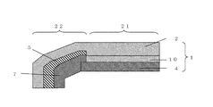
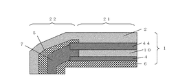
- a transparent conductive film layer 4 is formed on the inner surface of a transparent substrate 2 having a flat central portion 21 and an outer shape portion 22 standing up.
- This is a touch sensor with decoration on which the transparent conductive sensor 3 of the formed film base 6 is pasted.
- a transparent conductive film layer is formed on the inner surface of the transparent base 2 having a flat central portion 21 and an outer portion 22 standing up.
- Reference numeral 4 denotes a decorative touch sensor formed by transfer.
- an electrical signal from the circuit of the transparent conductive film layer 4 is applied to the rising shape portion of the outer portion 22.
- a routing circuit 7 to be detected and a decorative print layer 5 that covers the routing circuit 7 are formed.
- the polarizing film layer 10 is laminated and formed between the transparent substrate 2 and the transparent conductive film layer 4.
- the transparent substrate 2 is formed by processing a three-dimensional shape of soda glass, borosilicate glass, aluminosilicate glass, etc. in addition to a transparent resin molded product obtained by molding a transparent resin material such as polycarbonate, acrylic, or cycloolefin into a three-dimensional shape. A glass plate is mentioned.
- a transparent base material 2 having excellent strength is selected, the touch sensor 1 with decoration is thinned by reducing the thickness of the transparent base material 2, and an electronic device such as a mobile phone or a tablet including the touch sensor 1 with decoration is used. Thinning can be achieved.
- Chemically strengthened aluminosilicate glass is particularly preferred in that it has several times the pressure resistance compared to other materials and can be strengthened even when it is thin.
- molten aluminosilicate glass is immersed in a salt bath containing 85% by weight or more of a potassium salt, for example, potassium nitrate, and having a bath temperature of 300 to 600 ° C. for 1 to 15 hours, and is then immersed in the glass.
- a potassium salt for example, potassium nitrate
- the shape of the outer shape portion 22 is preferably a rising height of 1 to 5 mm, and the corner radius of the rising portion is a shape having a radius of 0.5 to 5 mm. preferable. This is because when the rising height is less than 1 mm, the frame is insufficiently narrowed, and when it is higher than 5 mm, it becomes difficult to bond. Further, by setting the corner radius of the rising portion to a radius of 0.5 mm or more, not only the external impact applied to the corner of the outer shape portion is dispersed and the transparent base material 2 is not easily broken, but also the transparent conductive material to be attached. There is an advantage that the sensor 3 and the transfer sheet 33 can easily follow and can be bonded easily.
- the transparent conductive sensor 3 to be attached to the transparent base material 2 will be described with reference to FIG.
- the transparent conductive sensor 3 at least the transparent conductive layer 4 is formed on the film substrate 6.
- the polarizing film layer 10 may be formed in advance on the transparent conductive film layer 4.
- a resin film such as polycarbonate, cycloolefin, acrylic, polyethylene terephthalate, polybutylene terephthalate, or the like can be used.
- the thickness of the film base is generally about 30 to 500 ⁇ m.
- the film substrate 6 referred to here is a substrate having bending characteristics with a bending stress of less than 150 MPa when the bending radius is 5 cm when a bending test is performed using a test apparatus of JIS K-7171.
- a material other than the resin film may be used.
- a flexible base material having bending characteristics comparable to the resin film such as non-alkali borosilicate glass having a thickness of 50 to 100 ⁇ m, is also included.
- the material for the transparent conductive film layer 4 generally, metal oxides such as tin oxide, indium oxide, antimony oxide, zinc oxide, cadmium oxide, and indium tin oxide (ITO) can be used. However, in the present invention, a part of the transparent conductive film layer 4 may be formed to follow the rising portion, so that it is preferable that the transparent conductive film layer 4 is formed of a material more flexible than these metal oxides.
- an ultrafine conductor fiber made of a conductive metal such as gold, silver, copper, tin, nickel, aluminum, palladium, or carbon (that is, metal nanofiber, metal nanowire, or carbon nanotube).
- transparent conductive films such as gold, silver, copper, tin, nickel, aluminum, palladium, etc., formed by patterning or self-organizing with fine wires that cannot be visually confirmed, and transparent in appearance
- a transparent conductive film made of a thiophene-based conductive polymer such as PEDOT (polyethylenedioxythiophene).
- the ultrafine conductor fibers having a cross-sectional diameter of 10 to 200 nm and an aspect ratio of 10 to 100,000 are preferable from the viewpoint of optical properties and conductivity.
- the transparent conductive film layer 4 can be patterned by a method in which the conductive fiber is contained in a transparent binder to form an ink by a general-purpose printing method, a method of forming a pattern by clear coating and forming a pattern by lift-off, or the like. .
- Examples of the conductive metal pattern that cannot be visually confirmed include a lattice pattern and a honeycomb pattern having a line width of 100 ⁇ m or less and an aperture ratio (a ratio in which a conductive metal pattern per unit area is not formed) of 90% or more.
- This pattern is formed by a method such as lift-off or etching.
- the pattern may be formed by a self-organization method combining a hydrophobic solvent-based solution cast film forming method and water vapor condensation phenomenon, or the pattern may be formed by a silver salt photographic technique.
- graphene when used as a transparent conductive film layer, there is a method of forming a pattern by a general-purpose printing method by adding it to the transparent binder, but copper, nickel, etc. on a film substrate having releasability
- a transparent conductive film with better quality is provided by providing a catalyst metal layer, forming graphene by a method such as CVD, patterning by lift-off, etc., transferring the transparent conductive film layer together with the catalyst metal layer, and removing the catalyst metal layer after transfer It is preferable at the point which can form a film layer.
- the catalyst metal layer is formed with a thickness of 10 to 80 nm by a method such as vacuum deposition, sputtering, ion plating, or plating.
- a CVD method plasma CVD is preferable because it can be formed at a low temperature.
- the method for removing the catalyst metal layer after the transfer include a method of immersing in an acid or alkali aqueous solution for several seconds and immediately washing with water.
- the transparent conductive film layer 4 has sufficient conductivity, it can be formed as it is to a terminal portion for connecting to an external circuit. However, since transparency and conductivity are generally in a contradictory relationship, it is preferable to separately form a routing circuit 7 for smoothly transmitting an electric signal except for the display portion.
- the routing circuit 7 is generally formed by forming a conductive ink such as silver paste by a general-purpose printing method, or by forming a conductive metal such as copper foil by a method such as lift-off or etching.
- Examples of the attaching method include a method in which the transparent conductive sensor 3 is placed on the transparent base material 2 and the film base material 6 is pressed and attached from the back surface with an elastic pad. In this method, since the elastic pad is freely deformed, it is possible to apply pressure even in a complicated shape of the transparent substrate 2 and to bond them together.
- the film is formed by moving the elastic rolls 12 while sequentially pressing them instead of the elastic pads. It is also possible to press and paste the substrate 6. In this method, since the rolls are moved while being sequentially pressed, the bonding can be performed at a high speed, so that productivity is improved. It is preferable that the transparent conductive sensor 3 be bent a little in advance in order to make it easier to follow.
- the pasting may be performed via an optically transparent double-sided tape (OCA) that is highly adhesive and optically transparent, or a tape (PSA) on which a pressure-sensitive adhesive is formed.
- OCA optically transparent double-sided tape
- PSA tape
- the main adhesive material is polymethacrylic acid.
- the elastic pad include a pad made of silicon rubber having a hardness of about 45-60.
- Examples of the elastic roll 12 include a roll made of silicon rubber having a hardness of about 60 to 90.
- the pressing force is preferably set to about 0.5 to 2 MPa.
- a transfer sheet 33 for transferring and forming the transparent conductive film layer 4 on the transparent substrate 2 will be described with reference to FIG.
- the transfer sheet 33 at least the transparent conductive film layer 4 is formed on a film substrate 36 having releasability, and an adhesive layer or the like is formed as necessary.
- the polarizing film layer 10 may be provided on the transparent conductive film layer 4 in advance.
- the material etc. of the transparent conductive film layer 4 and the polarizing film layer 10 the same as the above-mentioned transparent conductive sensor 3 may be sufficient.
- a resin film such as polyvinyl chloride, polypropylene, or polyethylene terephthalate that is inexpensive and excellent in workability may be used.
- the thickness of the film substrate is generally about 15 to 50 ⁇ m.
- the adhesive layer can be formed by general-purpose printing methods such as gravure, screen, offset, painting, dipping, reverse coating, etc.
- the main material of the adhesive layer when the transparent substrate 2 is a transparent resin material, acrylic, examples of the resin include vinyl, urethane, and epoxy.
- a resin such as polyamide and acrylic may be used, and a silane coupling agent may be added to improve adhesion.
- the transfer method is a method in which the transfer sheet 33 is placed on the transparent substrate 2 and the transfer sheet 33 is pressed from the back with an elastic pad to transfer and form the transparent conductive film layer 4 on the transparent substrate 2. Is mentioned. In this method, since the elastic pad is freely deformed, it is possible to apply pressure even when the transparent substrate has a complicated shape, and transfer can be formed. Examples of the elastic pad include a pad made of silicon rubber having a hardness of about 45-60. *
- the transfer is performed by moving the elastic roll 12 while sequentially pressing it instead of the elastic pad.
- the sheet 33 can be pressed and transferred.
- the transfer sheet 33 is narrowed down to a curved surface or a three-dimensional shape in advance.
- the elastic roll 12 include a roll made of silicon rubber having a hardness of about 60 to 90.
- the pressing force is preferably set to about 0.5 to 2 MPa.
- the transparent conductive sensor 3 and the transfer sheet 33 shown above are the cases where the transparent conductive film layer 4 is a single layer, a plurality of stacked layers may be formed.
- the transparent conductive film layer 4 may be formed on both the front and back surfaces of the film substrate 6.
- the transparent conductive film layer 4 and the routing circuit 7 are shown on the surface of the film base 6 on the transparent base 2 side. You may form in the surface side of the other side.
- the decorative print layer 5 not only functions as a frame of the flat central portion 21 corresponding to the display screen, but also functions to cover the routing circuit 7 that transmits the electrical signal of the transparent conductive film layer 4 to an external circuit. However, if the decorative print layer 5 is also formed on the flat central portion 21 of the transparent substrate 2, the display screen of the electronic device is reduced accordingly, so that the transparent substrate as shown in FIGS. Most preferably, the flat central portion 21 of the material 2 is a display screen having only the transparent conductive film layer 4 and is positioned and formed so that the frame of the decorative printing layer 5 is formed on the rising outer shape portion 22.
- the decorative print layer 5 is formed so that the central portion has a blank pattern and a frame-like pattern on the periphery thereof.
- the width and shape of the punched pattern at the center are set according to the width and shape of the input area and display area in the electronic device, but are preferably equal to the flat portion 21 of the transparent substrate 2.
- Examples of the method for forming the decorative print layer 5 on the outer shape part 22 include a method for forming the decorative print layer 5 as a constituent layer of the transparent conductive sensor 3 and the transfer sheet 33 described above.
- a step due to the thickness of the decorative printing layer 5 adversely affects the formation of the transparent conductive layer 4 and the routing circuit 7. It is necessary not to give.
- the decorative print layer 5 may be provided on the surface of the transparent substrate 2 separately from the transparent conductive sensor 3 and the transfer sheet 33. In that case, the inner surface of the transparent base material 2 may be sufficient, and an outer surface may be sufficient like FIG.
- the decorative print layer 5 may be formed directly on the transparent substrate 2 by a method such as tampo printing or mask coating, or may be previously applied to another transfer sheet by a method such as screen printing, gravure printing, or offset printing. After the decorative print layer 5 is formed, it may be provided on the transparent substrate 2 by a transfer method using a transfer pad or the like. Moreover, when the transparent base material 2 is a transparent molding resin base material, you may provide by the shaping
- the decorative print layer 5 uses a resin such as polyvinyl, polyamide, polyester, acrylic, polyurethane, polyvinyl acetal, polyester urethane, alkyd, etc. as a binder, and an appropriate color pigment or dye as a colorant. It is good to use the coloring ink to contain.
- the thickness of the decorative printing layer 5 is generally about 0.5 to 10 ⁇ m.
- the decorative print layer 5 may be a metal thin film layer or a combination of the metal thin film layer and the print layer.
- the metal thin film layer expresses metallic luster and is formed by a vacuum deposition method, a sputtering method, an ion plating method, a plating method, or the like.
- metals such as aluminum, nickel, gold, platinum, chromium iron, copper, tin, indium, silver, titanium, lead, and zinc, and alloys or compounds thereof can be used depending on the metallic luster color to be expressed.
- the thickness of the metal thin film layer is generally about 0.05 ⁇ m.
- a polarizing film layer 10 may be laminated between the transparent base material 2 and the transparent conductive film layer 4.
- the polarizing film layer 10 since the polarizing film layer 10 exhibits an antireflection effect, the light transmittance of the touch sensor 1 with decoration is improved, and the visibility of the display screen at the center is improved.
- another transparent conductive film layer 44 may be laminated between the transparent substrate 2 and the polarizing film layer 10.
- the polarizing film layer 10 is a film layer that transmits only light that vibrates in a certain direction, and is usually a layer in which a linear polarizing film and a retardation film are laminated.
- the linear polarizing film is a single layer. Including. Some of the light rays incident from the outside are reflected at the interface between the film base 6 and the transparent conductive film layer 3 and make it difficult to see the screen of a display such as an electronic device. At that time, the vibration direction of the light beam changes on the reflecting surface. Utilizing this property, the polarizing film layer 10 has an effect of blocking harmful reflected light rays that have been reflected at the interface and whose vibration direction has been changed, thereby reducing the reflectance and making the display screen easier to see.
- a linear polarizing film is a film that allows incident light to pass through only one of the orthogonally polarized components and shields the other by absorption (or reflection / scattering), and is a dichroic material such as iodine or organic dye on polyvinyl alcohol resin. Examples thereof include films obtained by dyeing and adsorbing materials, and highly stretched and oriented films, and triacetyl cellulose films. The thickness is about 10 to 100 ⁇ m.
- the retardation film is a film in which a predetermined strain is imparted to the transparent film by stretching or the like, and examples of the material of the transparent film include materials such as polycarbonate resin, cycloolefin resin, and liquid crystal polymer resin.
- the thickness is about 10 to 100 ⁇ m.
- the polarizing film layer 10 Rather than providing the polarizing film layer 10 on the entire surface, as shown in FIGS. 5 and 6, it is preferable to cut and form the polarizing film layer 10 only in a flat central portion corresponding to the vicinity of a display such as an electronic device in which polarization characteristics are particularly required. preferable. This is because the expensive polarizing film layer 10 is used without waste. Therefore, the touch sensor has excellent cost performance, and can be applied to middle-end electronic devices. Further, even when the touch sensor is attached to a transparent base material whose outer shape has a rising shape, the polarizing film layer 10 does not exist in the portion corresponding to the rising shape. This is because the desired polarization characteristic can be obtained without being stretched when 10 is attached.
- the cut cross section of the cut polarizing film layer 10 is inclined. This is because as the cut surface becomes oblique, it becomes easier to follow, so that the transparent conductive film layer 4 made of a material that is difficult to bend can be used, and the range of material selection is expanded. Moreover, it becomes difficult to generate defects such as wrinkles and bubble cavities caused by steps due to the polarizing film layer 10 that is cut when pasted on a transparent substrate, and productivity is improved.
- the cut pattern of the polarizing film layer 10 is set in accordance with the width and shape of the input area or display area of the electronic device or the like, but is slightly larger than that of the flat central portion of the transparent substrate 2. Is preferred. By doing so, there is no problem even if there is a slight misalignment in bonding.
- Examples of the method for cutting the polarizing film layer 10 include a method of cutting by irradiating a laser beam with carbon dioxide gas or the like in addition to punching with a sharp blade.
- a method of cutting by irradiating a laser beam with carbon dioxide gas or the like in addition to punching with a sharp blade.
- it is preferable to irradiate the laser beam from an oblique direction because it is easy to cut into an oblique cross section.
- the film base material 6 or mold release property is used as a method of laminating and forming the cut polarizing film layer 10 between the transparent base material 2 and the transparent conductive layer 4.
- a circuit of the transparent conductive film layer 4 is formed in the central window portion of the film base material 36, and the polarizing film layer 10 cut on the transparent conductive film layer 4 is laminated and formed on the frame portion around the central window portion.
- an optical transparent adhesive or pressure sensitive adhesive is applied on the polarizing film layer 10, or a separator is formed on both surfaces of the optical transparent adhesive layer in advance.
- the polarizing film layer 10 may be attached by peeling off one of the separators using the sheet that is used.
- the optical transparent adhesive layer include an acrylic resin adhesive layer having a thickness of 20 to 200 ⁇ m.
Landscapes
- Engineering & Computer Science (AREA)
- Chemical & Material Sciences (AREA)
- Physics & Mathematics (AREA)
- Chemical Kinetics & Catalysis (AREA)
- General Chemical & Material Sciences (AREA)
- Geochemistry & Mineralogy (AREA)
- Materials Engineering (AREA)
- Organic Chemistry (AREA)
- Life Sciences & Earth Sciences (AREA)
- Theoretical Computer Science (AREA)
- General Engineering & Computer Science (AREA)
- General Physics & Mathematics (AREA)
- Microelectronics & Electronic Packaging (AREA)
- Human Computer Interaction (AREA)
- Optics & Photonics (AREA)
- Fluid Mechanics (AREA)
- Ceramic Engineering (AREA)
- Inorganic Chemistry (AREA)
- Mechanical Engineering (AREA)
- Laminated Bodies (AREA)
- Position Input By Displaying (AREA)
Abstract
Description
2 透明基材
3 透明導電センサ
4 透明導電膜層
5 加飾印刷層
6 フィルム基材
7 引き回し回路
10 偏光フィルム層
12 弾性体のロール
21 中央部
22 外形部
33 転写シート
36 離型性を有するフィルム基材
44 別の透明導電膜層
Claims (14)
- 中央部は平坦で外形部は立ち上がり形状の透明基材の内側面に、透明導電膜層が形成されたフィルム基材の透明導電センサが貼り付け形成された装飾付きタッチセンサであって、中央部には透明導電膜層の回路が形成され、立ち上がり形状部には該透明導電膜層の回路からの電気信号を検出する引き回し回路及び該引き回し回路を覆い隠す加飾印刷層が形成されていることを特徴とする装飾付きタッチセンサ。
- 中央部は平坦で外形部は立ち上がり形状の透明基材の内側面に、透明導電膜層が転写形成された装飾付きタッチセンサであって、中央部には透明導電膜層の回路が形成され、立ち上がり形状部には該透明導電膜層の回路からの電気信号を検出する引き回し回路及び該引き回し回路を覆い隠す加飾印刷層が形成されていることを特徴とする装飾付きタッチセンサ。
- 前記加飾印刷層が立ち上がり形状の透明基材の外側面に形成されていることを特徴とする請求項1又は2に記載の装飾付きタッチセンサ。
- 前記透明基材と透明導電膜層との間に偏光フィルム層が積層形成されていることを特徴とする請求項1から3のいずれかに記載の装飾付きタッチセンサ。
- 別の透明導電膜層が、前記透明基材と偏光フィルム層との間に積層形成されていることを特徴とする請求項4に記載の装飾付きタッチセンサ。
- 前記透明導電膜層が、導電繊維及びチオフェン系導電ポリマーの少なくとも1つを含む、請求項1から5のいずれかに記載の装飾付きタッチセンサ。
- 前記透明導電膜層が、微細なメッシュパターン化させた金属膜、自己組織化させた金属微粒子パターン及びグラフェンの少なくとも1つを含む、請求項1から5のいずれかに記載の装飾付きタッチセンサ。
- 前記透明基材がアルミノケイ酸ガラスであり、外形部の立ち上がり形状を形成した後、化学処理を行って強度を向上させた化学強化ガラスであることを特徴とする請求項1から7のいずれかに記載の装飾付きタッチセンサ。
- 前記透明基材の立ち上がり形状が二次曲面であることを特徴とする請求項1から8のいずれかに記載の装飾付きタッチセンサ。
- 前記請求項4記載の装飾付きタッチセンサに用いるタッチセンサであって、フィルム基材または離型性を有するフィルム基材の中央部に透明導電膜層の回路が形成され、該透明導電膜層上にカットされた偏光フィルム層が積層形成され、前記中央部周囲の額縁部には該透明導電膜層の回路からの電気信号を検出する引き回し回路が形成されたタッチセンサ。
- 中央部は平坦で外形部は立ち上がり形状の透明基材の内側面に、透明導電膜層が形成されたフィルム基材の透明導電センサを載置し、背面から弾性体のロールを順次押圧しながら移動させることでもって該フィルム基材を押圧して貼り付け形成することを特徴とする装飾付きタッチセンサの製造方法。
- 中央部は平坦で外形部は立ち上がり形状の透明基材の内側面に、透明導電膜層が形成された転写シートを載置し、背面から弾性体のロールを順次押圧しながら移動させることでもって該転写シートを透明基材に押圧して積層後、転写シートの基材を剥離し、透明導電膜層を透明基材の内側面に、転写形成する請求項2から8のいずれかに記載の装飾付きタッチセンサの製造方法。
- 中央部は平坦で外形部は立ち上がり形状の透明基材の内側面に、透明導電膜層が形成された転写シートを載置し、背面から弾性体のパッドでもって該転写シートを透明基材に押圧して積層後、転写シートの基材を剥離し、透明導電膜層を透明基材の内側面に転写形成することを特徴とする装飾付きタッチセンサの製造方法。
- 前記透明導電膜層はグラフェンであって、転写シートの基材と透明導電膜層の間に触媒金属層が設けられ、該転写シートを透明基材に押圧して積層後、転写シートの基材を剥離し、触媒金属層、透明導電膜層を透明基材の内側面に転写形成した後、触媒金属層を除去することを特徴とする請求項7に記載の装飾付きタッチセンサの製造方法。
Priority Applications (3)
| Application Number | Priority Date | Filing Date | Title |
|---|---|---|---|
| CN201280062608.6A CN104024994B (zh) | 2011-12-22 | 2012-12-17 | 带装饰触摸传感器及其制造方法、以及其使用的触摸传感器 |
| US14/367,778 US9320140B2 (en) | 2011-12-22 | 2012-12-17 | Touch sensor with ornament, method of manufacturing same, and transparent conductive sensor used in same |
| KR1020147017302A KR101600871B1 (ko) | 2011-12-22 | 2012-12-17 | 장식 부착 터치 센서와 그 제조 방법, 및 거기에 사용되는 터치 센서 |
Applications Claiming Priority (4)
| Application Number | Priority Date | Filing Date | Title |
|---|---|---|---|
| JP2011281600A JP5464608B2 (ja) | 2011-12-22 | 2011-12-22 | 装飾付きタッチセンサ及びその製造方法 |
| JP2011-281600 | 2011-12-22 | ||
| JP2012-003961 | 2012-01-12 | ||
| JP2012003961A JP5464617B2 (ja) | 2012-01-12 | 2012-01-12 | 装飾付きタッチセンサ、及びその製造方法 |
Publications (1)
| Publication Number | Publication Date |
|---|---|
| WO2013094561A1 true WO2013094561A1 (ja) | 2013-06-27 |
Family
ID=48668451
Family Applications (1)
| Application Number | Title | Priority Date | Filing Date |
|---|---|---|---|
| PCT/JP2012/082663 Ceased WO2013094561A1 (ja) | 2011-12-22 | 2012-12-17 | 装飾付きタッチセンサとその製造方法、及びそれに用いるタッチセンサ |
Country Status (5)
| Country | Link |
|---|---|
| US (1) | US9320140B2 (ja) |
| KR (1) | KR101600871B1 (ja) |
| CN (1) | CN104024994B (ja) |
| TW (1) | TWI489339B (ja) |
| WO (1) | WO2013094561A1 (ja) |
Cited By (1)
| Publication number | Priority date | Publication date | Assignee | Title |
|---|---|---|---|---|
| CN103558934A (zh) * | 2013-09-27 | 2014-02-05 | 南昌欧菲光科技有限公司 | 触控显示模组及电子装置 |
Families Citing this family (16)
| Publication number | Priority date | Publication date | Assignee | Title |
|---|---|---|---|---|
| CN104571667B (zh) * | 2013-10-26 | 2018-05-29 | 宝宸(厦门)光学科技有限公司 | 触控面板及其制造方法 |
| KR102467260B1 (ko) * | 2014-08-27 | 2022-11-16 | 스미토모 긴조쿠 고잔 가부시키가이샤 | 적층체 필름과 전극 기판 필름 및 이들의 제조 방법 |
| CN107107656A (zh) * | 2015-01-06 | 2017-08-29 | 飞利浦照明控股有限公司 | 电子器件的液体浸渍转印方法 |
| CN104991672B (zh) * | 2015-07-06 | 2018-06-05 | 业成光电(深圳)有限公司 | 触摸装置及电子装置 |
| KR102391877B1 (ko) * | 2015-09-16 | 2022-04-29 | 솔브레인 주식회사 | 곡면부를 갖는 강화 유리 및 그 제조방법 |
| KR102376162B1 (ko) * | 2015-09-16 | 2022-03-21 | 솔브레인 주식회사 | 곡면부를 갖는 강화 유리, 강화 유리 필름 및 그 제조방법 |
| KR102679070B1 (ko) * | 2016-10-17 | 2024-07-02 | 삼성디스플레이 주식회사 | 터치 센서 및 이를 포함하는 표시 장치 |
| KR102741702B1 (ko) * | 2016-12-30 | 2024-12-12 | 엘지디스플레이 주식회사 | 스트레처블 터치 스크린, 이의 제조 방법 및 이를 이용한 표시 장치 |
| CN110402194B (zh) * | 2017-03-14 | 2022-04-29 | 松下知识产权经营株式会社 | 触摸传感器 |
| CN107167862A (zh) * | 2017-07-06 | 2017-09-15 | 京东方科技集团股份有限公司 | 偏光片、显示装置及偏光片的制备方法 |
| CN108045116B (zh) * | 2017-11-27 | 2019-06-28 | 江西合力泰科技有限公司 | 手机前盖板的丝印工艺 |
| US11304313B2 (en) | 2017-12-15 | 2022-04-12 | Hewlett-Packard Development Company, L.P. | Three-dimensional printing |
| JP2020119223A (ja) * | 2019-01-23 | 2020-08-06 | 尾池工業株式会社 | 加飾導電フィルム、抵抗膜式タッチパネルおよび電子機器 |
| DE102019127108A1 (de) * | 2019-10-09 | 2021-04-15 | Leonhard Kurz Stiftung & Co. Kg | Verfahren und Vorrichtung zur Herstellung eines Kunststoffbauteils sowie ein Kunststoffbauteil |
| EP3839617B1 (fr) | 2019-12-17 | 2024-06-26 | The Swatch Group Research and Development Ltd | Dispositif d affichage à cristaux liquides |
| CN111770675B (zh) * | 2020-06-19 | 2022-05-06 | 深圳市联得自动化装备股份有限公司 | 制作曲面模组的热压方法和热压设备、曲面模组和应用 |
Citations (3)
| Publication number | Priority date | Publication date | Assignee | Title |
|---|---|---|---|---|
| US20100284132A1 (en) * | 2009-05-08 | 2010-11-11 | Taiwan Green Point Enterprises Co., Ltd. | Touch panel module and method of making the same |
| JP2012043165A (ja) * | 2010-08-19 | 2012-03-01 | Alps Electric Co Ltd | 成形部材及び透光型入力装置 |
| JP2012208857A (ja) * | 2011-03-30 | 2012-10-25 | Alps Electric Co Ltd | 表面パネルおよびその製造方法 |
Family Cites Families (14)
| Publication number | Priority date | Publication date | Assignee | Title |
|---|---|---|---|---|
| JP4747747B2 (ja) * | 2005-09-08 | 2011-08-17 | ソニー株式会社 | 入力装置、その製造方法及び電子機器 |
| JP4624462B2 (ja) * | 2006-03-08 | 2011-02-02 | シャープ株式会社 | 表示装置 |
| KR101036044B1 (ko) * | 2007-05-31 | 2011-05-19 | 니혼샤신 인사츠 가부시키가이샤 | 인서트 성형용 적층물과 그 제조 방법, 인서트 성형품과 그 제조 방법 |
| KR100922737B1 (ko) * | 2007-12-18 | 2009-10-22 | 한국전자통신연구원 | 기가비트 이더넷(GbE) 신호를 광 전송 계위(OTH)구조에 정합하는 장치 |
| KR100894710B1 (ko) * | 2008-06-27 | 2009-04-24 | (주) 월드비젼 | 윈도우 일체형 터치스크린 및 이의 제조방법 |
| CN201247459Y (zh) * | 2008-08-25 | 2009-05-27 | 纬创资通股份有限公司 | 具有弯折成型的触控面板的触控式电子装置 |
| US20100097344A1 (en) * | 2008-10-16 | 2010-04-22 | Tpo Displays Corp. | Electronic apparatus with a capacitive touch sensor |
| WO2010074116A1 (ja) * | 2008-12-25 | 2010-07-01 | 日本写真印刷株式会社 | 押圧検出機能を有するタッチパネル及び当該タッチパネル用感圧センサ |
| JP4896178B2 (ja) | 2009-04-23 | 2012-03-14 | アルプス電気株式会社 | 座標入力装置及びそれを備えた画像表示装置と電子機器 |
| TW201040699A (en) * | 2009-05-08 | 2010-11-16 | Taiwan Green Point Entpr Co | Touch panel module and method of making the same |
| TW201120712A (en) * | 2009-12-09 | 2011-06-16 | J Touch Corp | Capacitive touch device structure. |
| TW201126377A (en) * | 2010-01-25 | 2011-08-01 | Artificial Muscle Inc | Electroactive polymer transducers for tactile feedback devices |
| KR101307296B1 (ko) * | 2010-06-22 | 2013-09-11 | 니폰샤신인사츠가부시키가이샤 | 방청성이 우수한 협소 프레임 터치 입력 시트와 그 제조 방법 |
| JP5774686B2 (ja) * | 2011-04-26 | 2015-09-09 | 日本メクトロン株式会社 | 透明プリント配線板の製造方法、および透明タッチパネルの製造方法 |
-
2012
- 2012-12-17 WO PCT/JP2012/082663 patent/WO2013094561A1/ja not_active Ceased
- 2012-12-17 CN CN201280062608.6A patent/CN104024994B/zh active Active
- 2012-12-17 KR KR1020147017302A patent/KR101600871B1/ko active Active
- 2012-12-17 US US14/367,778 patent/US9320140B2/en active Active
- 2012-12-20 TW TW101148645A patent/TWI489339B/zh not_active IP Right Cessation
Patent Citations (3)
| Publication number | Priority date | Publication date | Assignee | Title |
|---|---|---|---|---|
| US20100284132A1 (en) * | 2009-05-08 | 2010-11-11 | Taiwan Green Point Enterprises Co., Ltd. | Touch panel module and method of making the same |
| JP2012043165A (ja) * | 2010-08-19 | 2012-03-01 | Alps Electric Co Ltd | 成形部材及び透光型入力装置 |
| JP2012208857A (ja) * | 2011-03-30 | 2012-10-25 | Alps Electric Co Ltd | 表面パネルおよびその製造方法 |
Cited By (1)
| Publication number | Priority date | Publication date | Assignee | Title |
|---|---|---|---|---|
| CN103558934A (zh) * | 2013-09-27 | 2014-02-05 | 南昌欧菲光科技有限公司 | 触控显示模组及电子装置 |
Also Published As
| Publication number | Publication date |
|---|---|
| TWI489339B (zh) | 2015-06-21 |
| KR20140094642A (ko) | 2014-07-30 |
| US20150107881A1 (en) | 2015-04-23 |
| CN104024994B (zh) | 2017-02-22 |
| KR101600871B1 (ko) | 2016-03-08 |
| TW201342152A (zh) | 2013-10-16 |
| CN104024994A (zh) | 2014-09-03 |
| US9320140B2 (en) | 2016-04-19 |
Similar Documents
| Publication | Publication Date | Title |
|---|---|---|
| WO2013094561A1 (ja) | 装飾付きタッチセンサとその製造方法、及びそれに用いるタッチセンサ | |
| JP5464608B2 (ja) | 装飾付きタッチセンサ及びその製造方法 | |
| JP5066182B2 (ja) | インサート成形用積層物とその製造方法、インサート成形品とその製造方法 | |
| JP5746619B2 (ja) | ウィンドウパネル一体型静電容量式タッチセンサー及び製造方法 | |
| JP5916516B2 (ja) | 3次元曲面タッチパネル及びこれを用いた電子機器筐体 | |
| JP5906572B2 (ja) | 表示用前面板の製造方法、および表示装置の製造方法 | |
| US20110255227A1 (en) | Protection panel provided with touch input function for display window of electronic device, and manufacturing method therefor | |
| CN103631456B (zh) | 薄膜感应器、包含该感应器的电容触摸屏及其制作方法和终端产品 | |
| CN105117082B (zh) | 一种触摸屏的制作方法及触摸屏 | |
| JP5464617B2 (ja) | 装飾付きタッチセンサ、及びその製造方法 | |
| JP5805799B2 (ja) | タッチセンサおよびタッチセンサモジュール | |
| KR20140066742A (ko) | 박막 센서, 이를 갖는 용량형 터치 스크린 및 이의 준비 방법과 최종 제품 | |
| CN105324742A (zh) | 触摸屏显示单元及其制造方法 | |
| JP5754739B2 (ja) | タッチセンサ | |
| WO2003045125A1 (fr) | Materiau de fenetre transmettant la lumiere et protege contre les ondes electromagnetiques et procede de fabrication de ce materiau | |
| KR20150049174A (ko) | 터치센서 | |
| CN103543894A (zh) | 一种电容触摸屏及其制造方法 | |
| JP6416461B2 (ja) | タッチパネル用加飾カバー基材及びその製造方法 | |
| JP5768031B2 (ja) | 検知機能を有する表面パネル及びその製造方法 | |
| JP6192293B2 (ja) | カバーガラス一体型タッチセンサとその製造方法、及びそれに用いる積層用シート | |
| CN214751822U (zh) | 触控模组及采用该触控模组的触控显示屏 | |
| JP2012098973A (ja) | ガラス複合体及びそのガラス複合体を用いた入力装置 | |
| JP2007323092A (ja) | 電子機器表示窓の保護パネル及び保護パネルの製造方法 | |
| JP2015015015A (ja) | タッチセンサ用カバーシート、タッチセンサ用カバー基材、タッチセンサ及びタッチセンサ用カバーシートの製造方法 | |
| JP2014067365A (ja) | 検知機能を有する表面パネル |
Legal Events
| Date | Code | Title | Description |
|---|---|---|---|
| 121 | Ep: the epo has been informed by wipo that ep was designated in this application |
Ref document number: 12860255 Country of ref document: EP Kind code of ref document: A1 |
|
| WWE | Wipo information: entry into national phase |
Ref document number: 14367778 Country of ref document: US |
|
| NENP | Non-entry into the national phase |
Ref country code: DE |
|
| ENP | Entry into the national phase |
Ref document number: 20147017302 Country of ref document: KR Kind code of ref document: A |
|
| 122 | Ep: pct application non-entry in european phase |
Ref document number: 12860255 Country of ref document: EP Kind code of ref document: A1 |