WO2013077066A1 - インプリント用モールド及びその製造方法 - Google Patents
インプリント用モールド及びその製造方法 Download PDFInfo
- Publication number
- WO2013077066A1 WO2013077066A1 PCT/JP2012/073414 JP2012073414W WO2013077066A1 WO 2013077066 A1 WO2013077066 A1 WO 2013077066A1 JP 2012073414 W JP2012073414 W JP 2012073414W WO 2013077066 A1 WO2013077066 A1 WO 2013077066A1
- Authority
- WO
- WIPO (PCT)
- Prior art keywords
- layer
- substrate
- pattern
- mold
- main surface
- Prior art date
- Legal status (The legal status is an assumption and is not a legal conclusion. Google has not performed a legal analysis and makes no representation as to the accuracy of the status listed.)
- Ceased
Links
Images



Classifications
-
- B—PERFORMING OPERATIONS; TRANSPORTING
- B29—WORKING OF PLASTICS; WORKING OF SUBSTANCES IN A PLASTIC STATE IN GENERAL
- B29C—SHAPING OR JOINING OF PLASTICS; SHAPING OF MATERIAL IN A PLASTIC STATE, NOT OTHERWISE PROVIDED FOR; AFTER-TREATMENT OF THE SHAPED PRODUCTS, e.g. REPAIRING
- B29C59/00—Surface shaping of articles, e.g. embossing; Apparatus therefor
- B29C59/002—Component parts, details or accessories; Auxiliary operations
-
- G—PHYSICS
- G03—PHOTOGRAPHY; CINEMATOGRAPHY; ANALOGOUS TECHNIQUES USING WAVES OTHER THAN OPTICAL WAVES; ELECTROGRAPHY; HOLOGRAPHY
- G03F—PHOTOMECHANICAL PRODUCTION OF TEXTURED OR PATTERNED SURFACES, e.g. FOR PRINTING, FOR PROCESSING OF SEMICONDUCTOR DEVICES; MATERIALS THEREFOR; ORIGINALS THEREFOR; APPARATUS SPECIALLY ADAPTED THEREFOR
- G03F7/00—Photomechanical, e.g. photolithographic, production of textured or patterned surfaces, e.g. printing surfaces; Materials therefor, e.g. comprising photoresists; Apparatus specially adapted therefor
- G03F7/0002—Lithographic processes using patterning methods other than those involving the exposure to radiation, e.g. by stamping
-
- B—PERFORMING OPERATIONS; TRANSPORTING
- B29—WORKING OF PLASTICS; WORKING OF SUBSTANCES IN A PLASTIC STATE IN GENERAL
- B29C—SHAPING OR JOINING OF PLASTICS; SHAPING OF MATERIAL IN A PLASTIC STATE, NOT OTHERWISE PROVIDED FOR; AFTER-TREATMENT OF THE SHAPED PRODUCTS, e.g. REPAIRING
- B29C33/00—Moulds or cores; Details thereof or accessories therefor
- B29C33/56—Coatings, e.g. enameled or galvanised; Releasing, lubricating or separating agents
-
- B—PERFORMING OPERATIONS; TRANSPORTING
- B82—NANOTECHNOLOGY
- B82Y—SPECIFIC USES OR APPLICATIONS OF NANOSTRUCTURES; MEASUREMENT OR ANALYSIS OF NANOSTRUCTURES; MANUFACTURE OR TREATMENT OF NANOSTRUCTURES
- B82Y10/00—Nanotechnology for information processing, storage or transmission, e.g. quantum computing or single electron logic
-
- B—PERFORMING OPERATIONS; TRANSPORTING
- B82—NANOTECHNOLOGY
- B82Y—SPECIFIC USES OR APPLICATIONS OF NANOSTRUCTURES; MEASUREMENT OR ANALYSIS OF NANOSTRUCTURES; MANUFACTURE OR TREATMENT OF NANOSTRUCTURES
- B82Y40/00—Manufacture or treatment of nanostructures
-
- B—PERFORMING OPERATIONS; TRANSPORTING
- B29—WORKING OF PLASTICS; WORKING OF SUBSTANCES IN A PLASTIC STATE IN GENERAL
- B29L—INDEXING SCHEME ASSOCIATED WITH SUBCLASS B29C, RELATING TO PARTICULAR ARTICLES
- B29L2031/00—Other particular articles
- B29L2031/34—Electrical apparatus, e.g. sparking plugs or parts thereof
Definitions
- the present invention relates to an imprint mold and a method for manufacturing the same, and more particularly to an imprint mold having a concavo-convex pattern and a method for manufacturing the same.
- stepper by using light and an electron beam having a wavelength shorter than that of visible light from an ultraviolet laser or an extreme ultraviolet light source, processing from the micron order to several tens of nanometers becomes possible.
- micron-order processing takes a considerable amount of time to form a pattern. Therefore, the time required for nano-order microfabrication further increases.
- an ultraviolet laser or an extreme ultraviolet light source is used, the apparatus becomes large and the cost increases. Further, the technique of performing microfabrication by exposure / development with an electron beam is sequential processing, and the work efficiency is lowered.
- nanoimprint technology is a method of transferring a fine pattern onto a material to be transferred like a stamp using a mold in which a fine pattern of unevenness is formed.
- nanoimprint technology a fine structure of several tens of nm level can be manufactured at a low cost with good reproducibility and in large quantities.
- thermal imprinting is a method in which a mold on which a fine pattern is formed is pressed against a thermoplastic resin as a molding material while being heated, and then the molding material is cooled and released to transfer the fine pattern.
- Optical imprinting is a method in which a mold on which a fine pattern is formed is pressed against a photocurable resin that is a molding material, irradiated with ultraviolet light, and then the molding material is released to transfer the fine pattern. is there.
- Patent Document 4 there is an example in which a fine pattern made of amorphous carbon is formed on a planarizing layer.
- the amorphous carbon film that forms the convex portions of the fine pattern may be peeled off from the planarization layer during the etching for forming the fine pattern.
- Patent Document 4 even if the amorphous carbon film is peeled off from the planarization layer, it is possible to form a new amorphous carbon film and perform patterning again after peeling off the remaining amorphous carbon film. is there. That is, in the case of Patent Document 4, since the amorphous carbon film is used as the base of the fine pattern, the etching is relatively easy, and furthermore, the fine pattern can be easily reproduced by the above method.
- Patent Document 3 in the technique of directly plating copper on the main surface of the cylindrical substrate, copper cannot be plated depending on the type of the cylindrical substrate.
- the width is small but deep scratches are present on the main surface of the cylindrical substrate, it is possible that after the plating process, the scratched portion becomes a cavity, and copper may easily peel off from the main surface of the cylindrical substrate.
- the scratch is large, copper will be deposited along the shape of the scratch, and if a copper film with a considerable thickness is not formed, even if a fine pattern is formed on the copper film, the shape of the fine pattern will be There is also the possibility of being affected by the shape of the wound.
- An object of the present invention is to provide an imprint mold having a highly accurate concavo-convex pattern and a method of manufacturing the imprint mold which hardly causes peeling from a substrate.
- Patent Document 4 a planarizing layer is provided on a substrate, and a pattern layer is provided thereon. The pattern layer is peeled off from the planarization layer, thereby causing the above-described problem.
- the planarization layer has two functions: (Function 1) In the portion where the flattening layer is in contact with the substrate, the substrate is changed to a flat state by filling irregularities such as scratches on the main surface of the substrate.
- the first aspect of the present invention is: An imprint mold characterized by having a flattening agent layer in which a desired uneven pattern is formed on the outermost surface after filling irregularities (bumps) on the main surface of the substrate by applying a flattening agent.
- the base is a cylindrical substrate.
- the leveling agent layer is made of polysilazane.
- the fourth aspect of the present invention is: A leveling agent layer forming step of forming on the substrate a leveling agent layer that fills irregularities (bumps) on the main surface of the substrate by applying a leveling agent and planarizes the substrate; A pattern forming step of forming a desired concavo-convex pattern on the main surface of the planarizing agent layer itself; It is a manufacturing method of the mold for imprint characterized by having.
- the base is a cylindrical substrate.
- the leveling agent layer is made of polysilazane.
- Example 1 it is an optical microscope photograph of the main surface of the board
- A It is an external appearance photograph of the main surface of the board
- B It is an optical microscope photograph of the main surface of the board
- ⁇ Embodiment 1> a case where a mask layer and a resist layer are provided in this order over a planarizing agent layer will be described.
- ⁇ Embodiment 2> the case where a mask layer is not provided over the planarizing agent layer will be described.
- ⁇ Embodiment 3> modifications other than those described in the above embodiment will be described.
- “flat” indicates the surface roughness of the substrate, and indicates the amount of deviation from the geometric plane of the surface where there should be no scratch or the like.
- An index indicating “flatness” includes “flatness (roundness or flatness)”, which is an index defined in JIS B 0182.
- corrugated pattern is formed in what was originally used as a planarization layer. Therefore, what was originally used as a planarization layer is not flat at least on the outermost surface. Therefore, in the present embodiment, a layer having a planarizing function with respect to the main surface of the substrate and having an uneven pattern formed on the main surface is referred to as a “planarizing agent layer”.
- a factor that hinders the flattening of the main surface of the substrate is called unevenness. This is different from a desired uneven pattern formed on the main surface of the planarizing agent layer in the future.
- FIG. 1 is a diagram schematically showing a manufacturing process of an imprint mold 1 (hereinafter also simply referred to as a mold 1) in the present embodiment.
- FIG. 1A shows a base body (in this embodiment, a mold substrate 2 (hereinafter also simply referred to as a substrate 2)) as a base of the mold 1, and FIG. The mode that the leveling agent layer 6 is provided is shown.
- FIG. 1C shows a state in which a mask layer 8 and a resist layer 9 are sequentially formed on the planarizing agent layer 6, and
- FIG. 1D shows a desired pattern drawn on the resist layer 9.
- FIG. 1E shows a state where the mask layer 8 is etched to form a mask pattern 8 ′
- FIG. 1F shows that the planarizer layer 6 is etched to form the uneven pattern 6 ′.
- the state of forming is shown.
- FIG. 1G is a view showing a state in which the mold 1 is completed by performing cleaning after etching to remove the mask pattern 8 ′ and the resist pattern 9 ′.
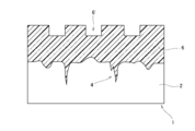
- FIG. 2 is a schematic cross-sectional view of the mold 1 in the present embodiment, and is an enlarged view of FIG. 1G, and a planarizing agent layer 6 is provided on the substrate 2.
- a mold 1 having a desired concavo-convex pattern 6 'on its main surface is obtained.
- the leveling agent layer 6 is a single layer, but the portion where the leveling agent layer 6 is in contact with the substrate 2 has irregularities 4 such as scratches on the main surface of the substrate 2. And the substrate 2 is changed to a flat state.
- a concavo-convex pattern 6 ′ is formed in a portion (a portion in contact with the atmosphere, that is, the outermost surface) facing the portion in which the planarizing layer is in contact with the substrate 2.
- FIG. 3 shows an overview when the mold 1 is used as a master mold.
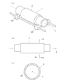
- 3A and 3B are schematic views of the mold 1 according to the present embodiment, in which FIG. 3A is a perspective view, FIG. 3B is a front view, and FIG. 3C is a cross-sectional view of the A-A ′ portion of FIG.
- FIGS. 3A and 3B are schematic views of the mold 1 according to the present embodiment, in which FIG. 3A is a perspective view, FIG. 3B is a front view, and FIG. 3C is a cross-sectional view of the A-A ′ portion of FIG.
- a substrate 2 as a substrate for a mold 1 is prepared.
- the “base” in the present embodiment includes a substrate as shown in the present specification and a substrate in which a hard mask is provided on the substrate.
- the substance includes a substrate, and refers to the substance itself that is to be provided with the planarizing agent layer 6.
- the substrate may have any composition as long as it can be used as the mold 1.
- an alloy substrate such as metal or stainless steel can be mentioned.
- glass substrates such as quartz substrates, SiC substrates, silicon wafer substrates, and silicon wafer substrates provided with an SiO 2 layer, graphite substrates, glassy carbon substrates, carbon fiber reinforced plastic (CFRP) carbon A system board
- the shape of the substrate 2 is not limited as long as it can be used as the mold 1.
- the shape of the substrate 2 includes a disk shape or a cylindrical shape. If it is disk shape, when apply
- the cylindrical shape is suitable for mass production because imprinting by a roller method is possible.
- the shape of the substrate 2 may be other than a disk shape, and may be a rectangle, a polygon, or a semicircle.
- examples of the shape of the substrate 2 include a polygonal shape such as a column, a triangular column, or a quadrangular column.
- the column or the cylinder type is uneven and uneven on the material to be transferred. It is more preferable because the pattern can be transferred.
- a substrate used as a basis for manufacturing an imprint mold is also referred to as a “substrate” regardless of the shape of the substrate 2.
- this substrate 2 has left and right mold end faces, a mold outer peripheral face 20, and a rotating shaft 3 that is not formed physically.
- leveling agent planarizing layer forming step
- the substrate used in the mold 1 may have micron-order scratches, and the micron-order scratches may greatly affect the reproducibility of the uneven pattern.
- the main surface of the substrate is flattened by a planarizing agent, instead of forming a concave / convex pattern directly on the main surface of the substrate 2 or separately providing a layer having the concave / convex pattern as in the prior art.
- a layer made of the planarized leveling agent (hereinafter also referred to as leveling agent layer 6) is formed on the substrate 2.
- leveling agent layer forming step will be described in detail.
- the “flattening agent” in the present embodiment can be applied to the main surface of the substrate, and can be any flattening obstruction factor (unevenness) present on the main surface of the substrate. good.
- this leveling agent include conventionally used liquid leveling film forming agents, and specific examples include polysilazane, methylsiloxane, and metal alkoxide.
- polysilazane methylsiloxane
- metal alkoxide metal alkoxide
- substances other than the above for example, positive resists composed of substituted naphthoquinonediazide and novolac resin, polystyrene, polymethyl methacrylate, polyvinylphenol, novolac resin, polyester, polyvinyl alcohol, polyethylene, polypropylene, polyimide, polybutadiene, polyvinyl acetate and polyvinyl Butyral or the like may be used.
- positive resists composed of substituted naphthoquinonediazide and novolac resin, polystyrene, polymethyl methacrylate, polyvinylphenol, novolac resin, polyester, polyvinyl alcohol, polyethylene, polypropylene, polyimide, polybutadiene, polyvinyl acetate and polyvinyl Butyral or the like may be used.
- the above-described materials may be used as the material constituting the leveling agent layer 6, or a mixture of the materials exemplified above may be used.
- the substrate 2 is held in a state where the rotating shaft 3 is horizontal, and a container containing a planarizing agent is prepared below the substrate 2. Thereafter, the substrate 2 is lowered, and a part of the outer peripheral surface of the substrate 2 is brought into contact with the planarizing agent. Then, a part of the substrate 2 is immersed in a planarizing agent.
- the substrate 2 is brought into contact with the planarizing agent in parallel with the rotation axis direction.
- the planarizing agent By making contact in parallel, it is possible to prevent a difference in the degree of application between the left and right mold end faces in the immersed portion of the substrate 2. As a result, unevenness is not caused in the application of the flattening agent.
- the substrate 2 is rotated by the plurality of rollers 107 to apply the planarizing agent to the mold outer peripheral surface 20 ( FIG. 1 (b)).
- a portion for rotating the substrate 2 by the roller 107 may be separately provided on the substrate 2. The rotation speed and rotation speed at this time are set so that the planarizing agent can be sufficiently applied to the substrate 2.
- the above method is applied to apply a planarizing agent to the substrate 2.
- the substrate 2 is planarized by filling the irregularities 4 on the main surface of the substrate by applying a planarizing agent.
- This “fill in the bumps” means that the recesses are filled at least.
- not only the scratches and dents are filled, but also the portions that are convex, and the portions that did not originally have any scratches or dents are also filled with the leveling agent layer. In this state, this state is preferable.
- the mask layer 8 any material may be used as the mask layer 8 as long as it has a function as a hard mask.
- the “hard mask” in the present embodiment refers to a layered layer composed of a single layer or a plurality of layers and used for etching on a substrate.
- the mask layer 8 is preferably an opaque layer.
- the transmittance of the mask layer 8 at a wavelength of 405 nm is preferably within an appropriate range.
- the “opaque layer” in the present embodiment is opaque to the extent that focusing is performed on the mask layer 8 when pattern drawing is focused on the substrate 2 on which the mask layer 8 is laminated. It means a certain layer.
- the mask layer 8 itself may be an opaque layer, or an opaque layer may be separately provided on the substrate 2.
- a chromium oxide layer (CrOx), a chromium nitride layer (CrNx), a chromium oxynitride layer (CrOxNy), a chromium and its compound containing carbon (CrOxNyCz), amorphous carbon
- CrOx chromium oxide layer
- CrNx chromium nitride layer
- CrOxNy chromium oxynitride layer
- CrOxNyCz a chromium and its compound containing carbon
- amorphous carbon Specific examples include amorphous carbon nitride and combinations thereof.
- the thickness of the chromium oxide layer is larger than 100 nm and the total thickness of the mask layer 8 is larger than 100 nm and 1 ⁇ m or less. If it is 100 nm or more, sufficient focusing can be performed on the chromium oxide layer. If it is 1 ⁇ m or more, it can withstand practical use during pattern transfer.
- the thickness of the chromium nitride layer is preferably 20 nm or more, and the total thickness of the mask layer 8 is preferably 20 nm or more and 1 ⁇ m or less.
- the thickness of the chromium nitride layer is more preferably 30 nm or more.
- the thickness of the chromium nitride layer is 20 nm or more, and the total thickness of the mask layer 8 is preferably 20 nm or more and 1 ⁇ m or less.
- amorphous carbon may be used. Since amorphous carbon does not have as high transparency as the chromium oxide layer, it is possible to prevent the substrate 2 from being focused on when the concave / convex pattern is drawn. In the case of amorphous carbon, it is preferable that the thickness of the amorphous carbon is greater than 50 nm, and the total thickness of the mask layer 8 is greater than 50 nm and 1 ⁇ m or less.
- the laser beam 109 can be reliably focused on the mask layer 8 formed on the surface of the planarizing agent layer 6. Further, if the thickness of the entire mask layer 8 is within the above range, the mask layer 8 can be reliably focused, and a concavo-convex pattern having an appropriate aspect ratio can be formed.
- a known method such as a sputtering method may be used.
- a resist is applied to the main surface of the mask layer 8.
- a coating method in this embodiment, a spin coating method is used in which a resist is coated from above the substrate 2 while rotating at a predetermined rotational speed.
- coating a resist the resist layer 9 is formed on the mask layer 8 by baking.
- a well-known thing may be sufficient and a chemically amplified resist may be sufficient. Any material having reactivity when irradiated with an energy beam may be used. Specifically, any resist that needs to be developed may be used. In this embodiment, a case where a positive resist used when pattern exposure by electron beam drawing is performed will be described. Note that when tungsten oxide (WOx) is used, laser drawing may be performed.
- WOx tungsten oxide
- the resist layer 9 is made of a positive resist, the solubility in the developer at the place where pattern exposure is performed by drawing with an electron beam, which will be described later, is improved, and the resist made of unevenness formed after development processing. It becomes a recessed part of pattern 9 ', and the part corresponds to the position of the recessed part in uneven
- the resist layer 9 is made of a negative resist, the pattern-exposed portion is cured and the solubility in the developer is reduced. As a result, a pattern having a correspondence relationship opposite to the concavo-convex relationship of the positive resist is formed.
- the adhesion layer 7 may be provided between the planarizing agent layer 6 and the mask layer 8 and / or between the mask layer 8 and the resist layer 9.
- An example of the adhesive layer 7 is amorphous silicon.
- the adhesion layer 7 may not be provided as long as the leveling agent layer 6, the mask layer 8, and the resist layer 9 can be favorably adhered.
- the pattern exposure in the present embodiment may be a known pattern exposure such as electron beam drawing or lithography. Further, the shape of the pattern is not limited, and may be a line shape, a dot shape (dot pattern), a mixed shape thereof, or the like. As an example, a desired fine pattern for manufacturing a bit patterned medium (BPM) is drawn on the resist layer 9 using an electron beam drawing machine. This fine pattern may be on the micron order, but it may be on the nano order from the viewpoint of the performance of electronic devices in recent years. Is preferred.
- a resist layer 9 for blue laser drawing may be formed on the mask layer 8 as described in b) Formation of the resist layer.
- the resist layer 9 for blue laser drawing may be a heat-sensitive material whose state changes due to a heat change, and may be suitable for the subsequent etching process. A photosensitive material may also be used.
- an inorganic resist layer made of tungsten oxide (WOx) having a composition gradient is more preferable from the viewpoint of improving resolution.
- the mask layer 8 is etched in the presence of the resist pattern 9 'to form a mask pattern 8' (FIG. 1 (e)).
- this etching method it may be determined according to the material of the mask layer 8, and dry etching, wet etching, or the like may be used according to the type of the mask layer 8. For example, when amorphous carbon is used for the mask layer, dry etching using O 2 gas may be performed. Further, the adhesion layer 7 is also etched as necessary.
- the desired concavo-convex pattern may be a pattern in the range from nano-order to micro-order, but is more preferably a nano-order periodic structure of several nm to several hundred nm. If a specific example is given, it is a fine protrusion structure consisting of a plurality of fine irregularities. Examples of the cross-sectional shape include a triangle, a trapezoid, and a square in the case of a one-dimensional periodic structure. In the case of a two-dimensional periodic structure, the shape of the fine protrusions is not limited to an accurate cone (bus line is straight) or pyramid (ridge line is straight), as long as it is tapered in consideration of extraction after imprinting.
- the ridgeline shape may be a curved surface with a side surface bulging outward. Specific examples include a bell, a cone, a truncated cone, and a cylinder. Furthermore, the tip portion may be flattened or rounded in consideration of moldability and breakage resistance. Further, this fine protrusion may be a continuous fine protrusion in one direction.
- the remaining resist pattern 9 ' is removed.
- the remaining mask pattern 8 ′ is removed using a method corresponding to the material of the mask layer.
- the resist pattern 9 ′ is made of WOx as in the present embodiment, the resist pattern 9 ′ is removed during the dry etching for polysilazane.
- the mask pattern 8 ′ is removed using O 2 gas as in the dry etching for the mask pattern 8 ′.
- the imprint mold according to the present embodiment is configured. According to the embodiment, the following effects can be obtained.
- the planarizing agent layer has the following two functions.
- (Function 1) In the portion where the flattening agent layer comes into contact with the substrate, irregularities such as scratches on the main surface of the substrate are filled to change the substrate into a flat state.
- (Function 2) On the outermost surface of the flattening agent layer (the surface facing the portion where the flattening agent layer contacts the substrate), a concavo-convex pattern to be transferred to the transfer target is formed.
- unevenness which is a factor that obstructs flattening of the main surface of the substrate
- unevenness can be filled by applying a flattening agent, and the upper portion of the main surface of the substrate can be made flat for the time being.
- unevenness (a part with no flaw and a part with a scratch) are buried in the main surface of the substrate with a planarizing agent layer, and electron beam drawing such as blue laser or electron beam (EB) is performed.
- EB electron beam drawing
- a desired concavo-convex pattern can be formed without being affected by irregularities (bumps) on the substrate.
- the mask layer 8 in the first embodiment plays a role of pattern transfer of the resist pattern 9 ′ to the planarizing agent layer 6, but as an opaque layer for focusing at the time of pattern drawing. It also has a role. Therefore, in the present embodiment, an opaque material is used as the leveling agent. By doing so, it is possible to prevent the pattern drawing from focusing on the rough surface substrate without using the mask layer 8 (opaque layer). That is, since the planarizing agent itself is opaque, the pattern drawing focus can be surely adjusted to the surface of the planarized planarizing agent layer 6.
- the leveling agent having opacity include a leveling agent to which a dye additive is added.
- the mold 1 is formed by forming the planarizing agent layer 6 and the mask layer 8 and then using the resist layer 9 is described.
- the mask pattern 8 ′ may be obtained by performing direct drawing on the mask layer 8.
- the uneven pattern may be directly formed on the planarizing agent layer 6 by direct drawing with an electron beam or the like without using the mask layer 8 or the resist layer 9.
- the planarizing agent layer 6 is formed by applying the planarizing agent to the entire main surface of the cylindrical substrate 2 has been described.
- the planarizing agent layer 6 may be partially formed on the main surface of the substrate 2 by partially applying the planarizing agent to the main surface of the substrate 2 instead of the entire main surface of the substrate 2.
- a plurality of leveling agent layers 6 may be formed on the main surface of the substrate 2.
- Example 1 An Example is shown and this invention is demonstrated concretely.
- a leveling agent was prepared.
- As the leveling agent a solution in which 20% of polysilazane was dissolved in dibutyl ether was used.
- a planarizing agent container containing the polysilazane solution was disposed below the substrate 2.
- the substrate 2 was brought into contact with the polysilazane solution.
- a part of the outer peripheral surface 20 of the mold was immersed in the flattening agent at a depth of 0.3 mm or less from the liquid surface of the flattening agent.
- the mold was rotated three times at a rotation speed of 32 rotations / minute by a separately provided rotating shaft 3, and the polysilazane solution was applied to the entire outer peripheral surface 20 of the mold.
- a polysilazane solution was applied onto the cylindrical substrate 2 so that the planarizing agent layer 6 had a thickness of 1.5 ⁇ m.
- the cylindrical substrate 2 and the planarizing agent were separated, and the substrate 2 was dried while being rotated.
- the mask layer 8 and the inorganic resist layer 9 were laminated in this order on the applied leveling agent layer 6.
- the adhesion layer 7 was not provided.
- an amorphous carbon film was formed to a thickness of 200 nm.
- a tungsten oxide (WOx) layer was formed to a thickness of 20 nm by sputtering.
- the flow rate ratio of Ar: O 2 was continuously changed by using an ion beam sputtering method to incline the oxygen concentration in the inorganic resist layer 9. Further, Rutherford Back Scattering Spectroscopy (RBS) was used for composition analysis in the inorganic resist layer 9.
- RBS Rutherford Back Scattering Spectroscopy
- a resist pattern 9 ′ was obtained.
- the mask layer 8 was dry-etched with O 2 gas to obtain a mask pattern 8 ′.
- the planarizing agent layer 6 made of polysilazane was dry-etched with Ar and CHF 3 gas to obtain a concavo-convex pattern 6 ′. Note that dry etching using O 2 gas was also used to remove the mask pattern 8 ′. Then, the washing process was performed and the mold 1 was produced. At this time, the etching depth of the concavo-convex pattern 6 ′ was 150 nm.
- Example 2 Using the same method as in Example 1, molds 1 having different pattern periods and drawing outputs when drawing a blue laser were produced in each Example. Specifically, in Example 2, the period is 160 nm and the output is 11.6 mW, in Example 3, the period is 140 nm and the output is 11.4 mW, in Example 4, the period is 120 nm and the output is 11.4 mW, and in Example 5, the period is The power was 100 nm and the output was 11.3 mW.
- Comparative Example 1 the planarizing agent layer was not provided on the substrate 2. That is, the same cylindrical hollow substrate 2 made of stainless steel as in Example 1 (SUS304, diameter of 100 mm, that is, radius of 50 mm, of which the diameter of the hollow portion is 84 mm, the distance between the mold end faces is 300 mm) is prepared. The inorganic resist layer 9 was laminated in this order. Other than that was the same as Example 1, and the mold 1 was produced.
- Example 1 is the state shown in FIG. 1C without the adhesion layer 7, that is, the mask layer 8 and the inorganic resist layer 9 are sequentially formed on the planarizing agent layer 6.
- Comparative Example 1 shows an appearance photograph and an optical microscope photograph (magnification 50 times) with respect to the main surface of the flattening agent layer 6, the mask layer 8 and the inorganic resist layer 9).
- FIG. 5A shows an appearance photograph of the substrate after application of the planarizing agent in Example 1
- FIG. 5B shows an optical microscope photograph.
- Example 1 can realize sufficient planarization.
- Examples 1 to 5 were observed with a scanning electron microscope (magnification of 50,000 times).
- FIGS. 7 (a) to (e) show photographs in plan view
- FIGS. 8 (a) to (e) show photographs in cross section.
- the CD (Critical Dimension) in the space portion of Example 1 was 99 nm
- the CD of Example 2 was 86 nm
- the CD of Example 2 was 66 nm
- the CD of Example 4 was 62 nm.
Landscapes
- Engineering & Computer Science (AREA)
- Chemical & Material Sciences (AREA)
- Nanotechnology (AREA)
- Physics & Mathematics (AREA)
- General Physics & Mathematics (AREA)
- Crystallography & Structural Chemistry (AREA)
- Theoretical Computer Science (AREA)
- Mathematical Physics (AREA)
- Condensed Matter Physics & Semiconductors (AREA)
- Mechanical Engineering (AREA)
- Manufacturing & Machinery (AREA)
- Exposure Of Semiconductors, Excluding Electron Or Ion Beam Exposure (AREA)
- Shaping Of Tube Ends By Bending Or Straightening (AREA)
- Moulds For Moulding Plastics Or The Like (AREA)
Abstract
Description
(機能1)平坦化層が基体と接触する部分においては、基体主表面にある傷などの凸凹(でこぼこ)を埋めて基体を平坦な状態に変える。
(機能2)平坦化層が基体と接触する部分と対向する部分(雰囲気と接触する部分、即ち最表面)においては、被転写体に転写されるべき凹凸パターンを形成する。
という機能を兼ね備えさせるという知見を得た。
本発明の第1の態様は、
平坦化剤の塗布により基体主表面の凸凹(でこぼこ)を埋めた上で、最表面には所望の凹凸パターンが形成されている平坦化剤層を有することを特徴とするインプリント用モールドである。
本発明の第2の態様は、第1の態様に記載の発明において、
前記基体は円筒型基板であることを特徴とする。
本発明の第3の態様は、第1又は第2の態様に記載の発明において、
前記平坦化剤層はポリシラザンからなることを特徴とする。
本発明の第4の態様は、
平坦化剤の塗布により基体主表面の凸凹(でこぼこ)を埋めて前記基体を平坦化する平坦化剤層を前記基体上に形成する平坦化剤層形成工程と、
前記平坦化剤層自体の主表面に所望の凹凸パターンを形成するパターン形成工程と、
を有することを特徴とするインプリント用モールドの製造方法である。
本発明の第5の態様は、第4の態様に記載の発明において、
前記基体は円筒型基板であることを特徴とする。
本発明の第6の態様は、第4又は第5の態様に記載の発明において、
前記平坦化剤層はポリシラザンからなることを特徴とする。
1.インプリント用モールド及びその製造方法
A)基板の準備
B)平坦化剤の塗布(平坦化剤層形成工程)
C)凹凸パターンの形成(凹凸パターン形成工程)
a)マスク層の形成
b)レジスト層の形成
c)パターン露光
d)現像(レジストパターンの形成)
e)リンス処理・乾燥
f)マスクパターンの形成
g)平坦化剤層への凹凸パターンの形成
h)マスクパターン及びレジストパターンの除去
i)洗浄等
2.実施の形態による効果
また、<実施の形態2>においては、平坦化剤層上にマスク層を設けない場合について説明する。
また、<実施の形態3>においては、上記の実施の形態で述べた以外の変形例について説明する。
また、本実施形態においては、本来は平坦化層として用いられていたものに凹凸パターンを形成している。故に、本来は平坦化層として用いられていたものは、少なくとも最表面においては平坦となっていない。そのため、本実施形態においては、基体の主表面に対する平坦化機能を有し且つ凹凸パターンを主表面に形成されている層のことを「平坦化剤層」と言う。
また、基体主表面の平坦化を阻害する要因(例えばキズや凹みによって主表面に生ずる段差)を、凸凹(でこぼこ)と言う。これは、将来的に平坦化剤層の主表面に形成される所望の凹凸パターンとは異なるものである。
(1.インプリント用モールド及びその製造方法)
以下、本実施形態について、図1を用いて説明する。図1は、本実施形態におけるインプリント用モールド1(以降、単にモールド1とも言う。)の製造工程を概略的に示す図である。図1(a)はモールド1の基となる基体(本実施形態においてはモールド基板2(以降、単に基板2とも言う。))を示し、図1(b)は基板2に平坦化剤よりなる平坦化剤層6を設けた様子を示す。更に、図1(c)はその平坦化剤層6の上にマスク層8、レジスト層9を順に形成した様子を示し、図1(d)はこのレジスト層9に対して所望のパターンを描画・現像してレジストパターン9’を形成した様子を示す。そして図1(e)はマスク層8に対してエッチングを行ってマスクパターン8’を形成した様子を示し、図1(f)は平坦化剤層6に対してエッチングを行って凹凸パターン6’を形成した様子を示す。そして、図1(g)は、エッチング後に洗浄を行い、マスクパターン8’及びレジストパターン9’を除去し、モールド1を完成させた様子を示す図である。
まず図1(a)に示すように、モールド1のための基体である基板2を用意する。なお、本実施形態における「基体」とは、本明細書に示すような基板、その基板の上にハードマスクが設けられたものを含む。まとめると、基板を含む物質であって、平坦化剤層6が設けられるべき対象となる物質そのものを指すものとする。
上述の通り、モールド1に用いられる基板にはミクロンオーダーの傷が存在するおそれがあり、このミクロンオーダーの傷が凹凸パターンの再現性に大きな影響を与えるおそれがある。
そのため、本実施形態においては、従来のように基板2の主表面に直接に凹凸パターンを形成したり、凹凸パターンを有する層を別途設けたりするのではなく、平坦化剤により基板主表面が平坦化された平坦化剤からなる層(以降、平坦化剤層6とも言う。)を基板2上に形成する。以下、この「平坦化剤層形成工程」について詳述する。
このときの回転速度及び回転数は、平坦化剤を基板2に十分塗布することができるように設定する。
本実施形態においては、上述のように塗布された平坦化剤からなる平坦化剤層6自体に凹凸パターンを形成することになる。以下、本実施形態においては、凹凸パターンを形成する一例について述べる。
凹凸パターンを形成するため、平坦化剤層6の上に、マスク層8を積層する。その後、マスク層8の上に、レジスト層9を積層する(図1(c))。
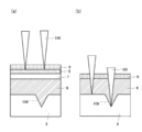
更に、マスク層8の波長405nmにおける透過率は適度な範囲内にあるのが好ましい。そうすることにより、図4(a)に示すように、マスク層8が積層された基板2の上部からレーザー光109を照射する際、パターン描画の際のレーザー光109のフォーカスをこのマスク層8上に確実に合わせることができる。より詳しく言うと、図4(b)に示すような事態を抑制、即ち、平坦化剤層6により折角基板2を平坦化したにも拘わらず、凹凸パターン描画の際のレーザー光109のフォーカスが、平坦化剤層6を通り越して粗表面基板上の傷108の部分に合わせられるのを抑制できる。
次に、マスク層8の主表面に対してレジストを塗布する。塗布方法としては、本実施形態においては所定の回転数にて回転させつつ基板2の上方からレジストを塗布するスピンコート法を用いる。このようにレジストを塗布した後、ベークを行うことにより、レジスト層9をマスク層8上に形成する。
本実施形態におけるパターン露光は、電子線描画やリソグラフィー等、公知のパターン露光であれば良い。また、パターンの形状についても限定はなく、線状・点状(ドットパターン)・それらの混合等形状等であっても良い。一例を挙げるとすれば、電子線描画機を用いて、レジスト層9に対して、ビットパターンドメディア(BPM)製造用の所望の微細パターンを描画することが挙げられる。この微細パターンはミクロンオーダーであっても良いが、近年の電子機器の性能という観点からはナノオーダーであっても良いし、パターン付き基体などにより作製される最終製品の性能を考えると、その方が好ましい。
描画済みのレジスト層9を有する基板2に対して現像を行うことにより、図1(d)に示すように、所望の凹凸からなるレジストパターン9’が得られる。なお、本実施形態における現像処理についても、公知のやり方であれば良い。
レジストパターン9’を有する基板2に対し、必要に応じてリンス処理を行った後、乾燥処理(ベーク)等を行う。
その後、レジストパターン9’が存在する状況でマスク層8をエッチングし、マスクパターン8’を形成する(図1(e))。なお、このエッチングの方法においては、マスク層8の物質に応じて決定すれば良く、ドライエッチングやウェットエッチング等をマスク層8の種類に応じて使用すれば良い。例えば、マスク層にアモルファスカーボンを用いた場合は、O2ガスを用いたドライエッチングを行えば良い。また、必要に応じて密着層7に対してもエッチングを行う。
そして、マスクパターン8’ が存在する状況で平坦化剤層6をエッチングする。その結果、所望の凹凸パターン6’を平坦化剤層6に形成することができる(図1(f))。なお、このエッチング方法としては、平坦化剤の種類に応じて決定すれば良い。例えば平坦化剤としてポリシラザンを用いた場合は、一例として挙げるとすると、Ar及びCHF3ガスにてドライエッチングを行えば良い。なお、ウェットエッチングを行う場合は、バッファードフッ酸を用いることも考えられる。
更には、成形性や耐破損性を考慮して、先端部を平坦にしたり、丸みをつけたりしても良い。更に、この微細突起は一方向に対して連続的な微細突起を作製しても良い。
その後、残存したレジストパターン9’を除去する。同様に、マスク層の物質に応じた手法を用い、残存したマスクパターン8’を除去する。なお、本実施形態のようにレジストパターン9’がWOxからなる場合、ポリシラザンに対する上記のドライエッチングの際に、レジストパターン9’を除去する。また、マスクパターン8’については、マスクパターン8’に対するドライエッチングと同様、O2ガスを用い、マスクパターン8’を除去する。
以上の工程を経た後、必要があれば基板2の洗浄等を行う。このようにして、凹凸パターンを主表面に有する平坦化剤層6を形成し、モールド1を完成させる(図1(g))。
以上のように、本実施形態に係るインプリント用モールドが構成される。実施の形態によれば、以下の効果を奏する。
(機能1)平坦化剤層が基体と接触する部分においては、基体主表面にある傷などの凸凹(でこぼこ)を埋めて基体を平坦な状態に変える。
(機能2)平坦化剤層の最表面(平坦化剤層が基体と接触する部分と対向する面)においては、被転写体に転写されるべき凹凸パターンを形成する。
実施の形態1においては、マスク層8を設けた場合について述べた。本実施形態においては、マスク層8を設けずに、平坦化剤層6の上に直接(又は密着層7の上に)レジスト層9を設ける場合について述べる。
実施の形態1においては、平坦化剤層6及びマスク層8を形成した後、レジスト層9を形成しこれを利用することによりモールド1を作製する場合について述べた。本実施形態においては、マスク層8にアモルファスカーボンを用いた場合、マスク層8に対して直接描画を行い、マスクパターン8’を得ても良い。
更に、平坦化剤層6に対し、電子線等による直接描画により、マスク層8やレジスト層9を介さずに、凹凸パターンを直接形成しても良い。
次に実施例を示し、本発明について具体的に説明する。
ステンレス製の円筒型の中空基板2(SUS304、直径100mm即ち半径50mm、そのうち中空部分の直径84mm、モールド端面間距離300mm)を用意した。
その後、円筒型の基板2と平坦化剤とを引き離し、基板2を回転させながら乾燥させた。
マスク層8としてはアモルファスカーボンを200nmの厚さで成膜した。無機レジスト層9としては酸化タングステン(WOx)層をスパッタ法により、20nmの厚さで成膜した。なお、無機レジスト層9の深さ方向への組成変化については、基板側x=0.95、レジスト最表面側x=1.60の傾斜組成とした。この無機レジスト層9の形成には、イオンビームスパッタ法を用いてAr:O2の流量比を連続的に変化させて無機レジスト層9中の酸素濃度を傾斜させた。また、無機レジスト層9中の組成分析にはラザフォード後方散乱分光法(Rutherford Back Scattering Spectroscopy:RBS)を使用した。
実施例1と同様の手法を用い、青色レーザーを描画する際のパターンの周期及び描画出力を変えたモールド1を各々の実施例にて作製した。具体的に言うと、実施例2では周期160nm及び出力11.6mWとし、実施例3では周期140nm及び出力11.4mWとし、実施例4では周期120nm及び出力11.4mWとし、実施例5では周期100nm及び出力11.3mWとした。
比較例1においては、基板2に対し、平坦化剤層を設けなかった。つまり、実施例1と同様のステンレス製の円筒型の中空基板2(SUS304、直径100mm即ち半径50mm、そのうち中空部分の直径84mm、モールド端面間距離300mm)を用意し、その上にマスク層8、無機レジスト層9をこの順に積層した。それ以外は実施例1と同様とし、モールド1を作製した。
実施例1及び比較例1における未パターニングの基板(実施例1は密着層7抜きの図1(c)の状態、即ち平坦化剤層6の上にマスク層8、無機レジスト層9を順次形成した状態である一方、比較例1は平坦化剤層6、マスク層8、無機レジスト層9のいずれも形成していない状態)の主表面に対し、外観写真及び光学顕微鏡写真(倍率50倍)を撮影した。実施例1における平坦化剤塗布後の基板の外観写真を図5(a)、光学顕微鏡写真を図5(b)に示す。また、比較例1における基板の外観写真を図6(a)、光学顕微鏡写真を図6(b)に示す。この結果を見比べると、外観写真及び光学顕微鏡写真というレベルのスケールにおいても、実施例1の方が、充分な平坦化が実現できていることがわかる。
その結果、いずれの実施例においても、モールド1の主表面においては精度の高い凹凸パターンが形成されており、フォーカス異常は生じていないことが確認できた。
2 モールド基板(基板)
20 モールド外周面
3 回転軸
4 凸凹(でこぼこ)
6 平坦化剤層
6’ 凹凸パターン
7 密着層
8 マスク層
8’ マスクパターン
9 レジスト層
9’ レジストパターン
107 ローラー
108 基板主表面の傷
109 レーザー光
Claims (6)
- 平坦化剤の塗布により基体主表面の凸凹(でこぼこ)を埋めた上で、最表面には所望の凹凸パターンが形成されている平坦化剤層を有することを特徴とするインプリント用モールド。
- 前記基体は円筒型基板であることを特徴とする請求項1に記載のインプリント用モールド。
- 前記平坦化剤層はポリシラザンからなることを特徴とする請求項1又は2に記載のインプリント用モールド。
- 平坦化剤の塗布により基体主表面の凸凹(でこぼこ)を埋めて前記基体を平坦化する平坦化剤層を前記基体上に形成する平坦化剤層形成工程と、
前記平坦化剤層自体の主表面に所望の凹凸パターンを形成するパターン形成工程と、
を有することを特徴とするインプリント用モールドの製造方法。 - 前記基体は円筒型基板であることを特徴とする請求項4に記載のインプリント用モールドの製造方法。
- 前記平坦化剤層はポリシラザンからなることを特徴とする請求項4又は5に記載のインプリント用モールドの製造方法。
Priority Applications (3)
| Application Number | Priority Date | Filing Date | Title |
|---|---|---|---|
| SG11201404231WA SG11201404231WA (en) | 2011-11-25 | 2012-09-13 | Mold for imprint and method for manufacturing the same |
| US14/360,816 US20140342030A1 (en) | 2011-11-25 | 2012-09-13 | Mold for imprint and method for manufacturing the same |
| KR20147017363A KR20140095102A (ko) | 2011-11-25 | 2012-09-13 | 임프린트용 몰드 및 그 제조 방법 |
Applications Claiming Priority (2)
| Application Number | Priority Date | Filing Date | Title |
|---|---|---|---|
| JP2011-257100 | 2011-11-25 | ||
| JP2011257100A JP5441991B2 (ja) | 2011-11-25 | 2011-11-25 | インプリント用モールド及びその製造方法 |
Publications (1)
| Publication Number | Publication Date |
|---|---|
| WO2013077066A1 true WO2013077066A1 (ja) | 2013-05-30 |
Family
ID=48469524
Family Applications (1)
| Application Number | Title | Priority Date | Filing Date |
|---|---|---|---|
| PCT/JP2012/073414 Ceased WO2013077066A1 (ja) | 2011-11-25 | 2012-09-13 | インプリント用モールド及びその製造方法 |
Country Status (5)
| Country | Link |
|---|---|
| US (1) | US20140342030A1 (ja) |
| JP (1) | JP5441991B2 (ja) |
| KR (1) | KR20140095102A (ja) |
| SG (1) | SG11201404231WA (ja) |
| WO (1) | WO2013077066A1 (ja) |
Cited By (1)
| Publication number | Priority date | Publication date | Assignee | Title |
|---|---|---|---|---|
| US9800063B2 (en) | 2013-09-12 | 2017-10-24 | Murata Manufacturing Co., Ltd. | Power transmission device and wireless power transmission system |
Families Citing this family (5)
| Publication number | Priority date | Publication date | Assignee | Title |
|---|---|---|---|---|
| KR20140076357A (ko) * | 2012-12-12 | 2014-06-20 | 삼성전자주식회사 | 고대비 정렬 마크를 가진 나노임프린트 스탬프 및 그 제조방법 |
| JP6437387B2 (ja) | 2015-05-25 | 2018-12-12 | 東芝メモリ株式会社 | 基板平坦化方法 |
| US10032633B1 (en) * | 2017-01-17 | 2018-07-24 | International Business Machines Corporation | Image transfer using EUV lithographic structure and double patterning process |
| US11365705B2 (en) | 2018-10-25 | 2022-06-21 | The Boeing Company | Laminates of polysilazane and carbon fiber reinforced polymer |
| JP7358425B2 (ja) * | 2021-08-18 | 2023-10-10 | 三菱重工業株式会社 | 複合材の加工装置及び複合材の加工方法 |
Citations (4)
| Publication number | Priority date | Publication date | Assignee | Title |
|---|---|---|---|---|
| JP2001310330A (ja) * | 2000-04-27 | 2001-11-06 | Hitachi Koki Co Ltd | 金型及びその成形品 |
| JP2010240864A (ja) * | 2009-04-01 | 2010-10-28 | Tocalo Co Ltd | インプリント部材の製造方法およびインプリント部材 |
| WO2011093356A1 (ja) * | 2010-01-29 | 2011-08-04 | Hoya株式会社 | インプリント用回転式モールド及びその製造方法 |
| WO2011093357A1 (ja) * | 2010-01-29 | 2011-08-04 | Hoya株式会社 | インプリント用モールド及びその製造方法 |
-
2011
- 2011-11-25 JP JP2011257100A patent/JP5441991B2/ja active Active
-
2012
- 2012-09-13 WO PCT/JP2012/073414 patent/WO2013077066A1/ja not_active Ceased
- 2012-09-13 US US14/360,816 patent/US20140342030A1/en not_active Abandoned
- 2012-09-13 SG SG11201404231WA patent/SG11201404231WA/en unknown
- 2012-09-13 KR KR20147017363A patent/KR20140095102A/ko not_active Withdrawn
Patent Citations (4)
| Publication number | Priority date | Publication date | Assignee | Title |
|---|---|---|---|---|
| JP2001310330A (ja) * | 2000-04-27 | 2001-11-06 | Hitachi Koki Co Ltd | 金型及びその成形品 |
| JP2010240864A (ja) * | 2009-04-01 | 2010-10-28 | Tocalo Co Ltd | インプリント部材の製造方法およびインプリント部材 |
| WO2011093356A1 (ja) * | 2010-01-29 | 2011-08-04 | Hoya株式会社 | インプリント用回転式モールド及びその製造方法 |
| WO2011093357A1 (ja) * | 2010-01-29 | 2011-08-04 | Hoya株式会社 | インプリント用モールド及びその製造方法 |
Cited By (1)
| Publication number | Priority date | Publication date | Assignee | Title |
|---|---|---|---|---|
| US9800063B2 (en) | 2013-09-12 | 2017-10-24 | Murata Manufacturing Co., Ltd. | Power transmission device and wireless power transmission system |
Also Published As
| Publication number | Publication date |
|---|---|
| US20140342030A1 (en) | 2014-11-20 |
| JP5441991B2 (ja) | 2014-03-12 |
| JP2013111763A (ja) | 2013-06-10 |
| KR20140095102A (ko) | 2014-07-31 |
| SG11201404231WA (en) | 2014-10-30 |
Similar Documents
| Publication | Publication Date | Title |
|---|---|---|
| JP5677987B2 (ja) | インプリント用モールド及びその製造方法、並びにインプリント用モールド基材 | |
| JP5441991B2 (ja) | インプリント用モールド及びその製造方法 | |
| JP6725097B2 (ja) | フィルムマスク、その製造方法、これを用いたパターンの形成方法およびこれを用いて形成されたパターン | |
| JP5935385B2 (ja) | ナノインプリント用レプリカテンプレートの製造方法及びレプリカテンプレート | |
| JP5935453B2 (ja) | 基板の製造方法、および、ナノインプリントリソグラフィ用テンプレートの製造方法 | |
| CN101952093A (zh) | 无缝塑模的制造方法 | |
| JP2013035243A (ja) | ローラーモールド、ローラーモールド用基材及びパターン転写方法 | |
| CN105408265B (zh) | 圆筒基体材料、原盘及原盘的制造方法 | |
| JP2008198746A (ja) | インプリントモールド、これを用いたインプリント評価装置、レジストパターン形成方法及びインプリントモールドの製造方法 | |
| JP5200726B2 (ja) | インプリント方法、プレインプリントモールド、プレインプリントモールド製造方法、インプリント装置 | |
| JP2024116304A (ja) | 原盤、原盤の製造方法及び転写物の製造方法 | |
| CN106547044B (zh) | 一种偏光片的加工设备及制造方法 | |
| JP2013180508A (ja) | インプリント用のモールドおよび微細構造の形成方法 | |
| JP5707342B2 (ja) | インプリント用回転式モールド及びその製造方法 | |
| JP6996333B2 (ja) | ブランクス基材、インプリントモールド、インプリントモールドの製造方法及びインプリント方法 | |
| JP6757241B2 (ja) | パターン形成方法及びレプリカモールドの製造方法 | |
| JP6417728B2 (ja) | テンプレートの製造方法 | |
| TW202330233A (zh) | 模具、模具之製造方法及微細凹凸結構體之製造方法 | |
| JP2007035998A (ja) | インプリント用モールド | |
| JP7504574B2 (ja) | 原盤、原盤の製造方法及び転写物の製造方法 | |
| JP7110598B2 (ja) | インプリントモールド及びその製造方法 | |
| JP2018157144A (ja) | インプリントモールド用マスクブランク及びその製造方法、インプリントモールド及びその製造方法、並びにインプリント方法 | |
| JP2023146116A (ja) | 基材及び基材の製造方法、並びに原盤及び原盤の製造方法 | |
| TWI626516B (zh) | Manufacturing method of micron-sized imprinting mold and imprinting mold | |
| CN121679952A (zh) | 一种配向膜的制备方法 |
Legal Events
| Date | Code | Title | Description |
|---|---|---|---|
| 121 | Ep: the epo has been informed by wipo that ep was designated in this application |
Ref document number: 12851013 Country of ref document: EP Kind code of ref document: A1 |
|
| NENP | Non-entry into the national phase |
Ref country code: DE |
|
| ENP | Entry into the national phase |
Ref document number: 20147017363 Country of ref document: KR Kind code of ref document: A |
|
| WWE | Wipo information: entry into national phase |
Ref document number: 14360816 Country of ref document: US |
|
| 122 | Ep: pct application non-entry in european phase |
Ref document number: 12851013 Country of ref document: EP Kind code of ref document: A1 |