WO2013076830A1 - Composant électronique et procédé de production de celui-ci - Google Patents
Composant électronique et procédé de production de celui-ci Download PDFInfo
- Publication number
- WO2013076830A1 WO2013076830A1 PCT/JP2011/076962 JP2011076962W WO2013076830A1 WO 2013076830 A1 WO2013076830 A1 WO 2013076830A1 JP 2011076962 W JP2011076962 W JP 2011076962W WO 2013076830 A1 WO2013076830 A1 WO 2013076830A1
- Authority
- WO
- WIPO (PCT)
- Prior art keywords
- side wall
- substrate
- outer periphery
- electronic component
- wafer
- Prior art date
Links
Images


Classifications
-
- H—ELECTRICITY
- H03—ELECTRONIC CIRCUITRY
- H03H—IMPEDANCE NETWORKS, e.g. RESONANT CIRCUITS; RESONATORS
- H03H9/00—Networks comprising electromechanical or electro-acoustic devices; Electromechanical resonators
- H03H9/02—Details
- H03H9/05—Holders; Supports
- H03H9/10—Mounting in enclosures
- H03H9/1057—Mounting in enclosures for microelectro-mechanical devices
-
- H—ELECTRICITY
- H01—ELECTRIC ELEMENTS
- H01L—SEMICONDUCTOR DEVICES NOT COVERED BY CLASS H10
- H01L23/00—Details of semiconductor or other solid state devices
- H01L23/02—Containers; Seals
- H01L23/04—Containers; Seals characterised by the shape of the container or parts, e.g. caps, walls
-
- B—PERFORMING OPERATIONS; TRANSPORTING
- B23—MACHINE TOOLS; METAL-WORKING NOT OTHERWISE PROVIDED FOR
- B23K—SOLDERING OR UNSOLDERING; WELDING; CLADDING OR PLATING BY SOLDERING OR WELDING; CUTTING BY APPLYING HEAT LOCALLY, e.g. FLAME CUTTING; WORKING BY LASER BEAM
- B23K1/00—Soldering, e.g. brazing, or unsoldering
- B23K1/0008—Soldering, e.g. brazing, or unsoldering specially adapted for particular articles or work
- B23K1/0016—Brazing of electronic components
-
- B—PERFORMING OPERATIONS; TRANSPORTING
- B81—MICROSTRUCTURAL TECHNOLOGY
- B81B—MICROSTRUCTURAL DEVICES OR SYSTEMS, e.g. MICROMECHANICAL DEVICES
- B81B7/00—Microstructural systems; Auxiliary parts of microstructural devices or systems
- B81B7/0032—Packages or encapsulation
- B81B7/0035—Packages or encapsulation for maintaining a controlled atmosphere inside of the chamber containing the MEMS
- B81B7/0041—Packages or encapsulation for maintaining a controlled atmosphere inside of the chamber containing the MEMS maintaining a controlled atmosphere with techniques not provided for in B81B7/0038
-
- B—PERFORMING OPERATIONS; TRANSPORTING
- B81—MICROSTRUCTURAL TECHNOLOGY
- B81C—PROCESSES OR APPARATUS SPECIALLY ADAPTED FOR THE MANUFACTURE OR TREATMENT OF MICROSTRUCTURAL DEVICES OR SYSTEMS
- B81C1/00—Manufacture or treatment of devices or systems in or on a substrate
- B81C1/00865—Multistep processes for the separation of wafers into individual elements
- B81C1/00873—Multistep processes for the separation of wafers into individual elements characterised by special arrangements of the devices, allowing an easier separation
-
- H—ELECTRICITY
- H01—ELECTRIC ELEMENTS
- H01L—SEMICONDUCTOR DEVICES NOT COVERED BY CLASS H10
- H01L24/00—Arrangements for connecting or disconnecting semiconductor or solid-state bodies; Methods or apparatus related thereto
- H01L24/93—Batch processes
- H01L24/94—Batch processes at wafer-level, i.e. with connecting carried out on a wafer comprising a plurality of undiced individual devices
-
- B—PERFORMING OPERATIONS; TRANSPORTING
- B23—MACHINE TOOLS; METAL-WORKING NOT OTHERWISE PROVIDED FOR
- B23K—SOLDERING OR UNSOLDERING; WELDING; CLADDING OR PLATING BY SOLDERING OR WELDING; CUTTING BY APPLYING HEAT LOCALLY, e.g. FLAME CUTTING; WORKING BY LASER BEAM
- B23K2101/00—Articles made by soldering, welding or cutting
- B23K2101/36—Electric or electronic devices
- B23K2101/42—Printed circuits
-
- B—PERFORMING OPERATIONS; TRANSPORTING
- B81—MICROSTRUCTURAL TECHNOLOGY
- B81B—MICROSTRUCTURAL DEVICES OR SYSTEMS, e.g. MICROMECHANICAL DEVICES
- B81B2201/00—Specific applications of microelectromechanical systems
- B81B2201/01—Switches
- B81B2201/012—Switches characterised by the shape
- B81B2201/014—Switches characterised by the shape having a cantilever fixed on one side connected to one or more dimples
-
- H—ELECTRICITY
- H01—ELECTRIC ELEMENTS
- H01L—SEMICONDUCTOR DEVICES NOT COVERED BY CLASS H10
- H01L21/00—Processes or apparatus adapted for the manufacture or treatment of semiconductor or solid state devices or of parts thereof
- H01L21/02—Manufacture or treatment of semiconductor devices or of parts thereof
- H01L21/04—Manufacture or treatment of semiconductor devices or of parts thereof the devices having at least one potential-jump barrier or surface barrier, e.g. PN junction, depletion layer or carrier concentration layer
- H01L21/50—Assembly of semiconductor devices using processes or apparatus not provided for in a single one of the subgroups H01L21/06 - H01L21/326, e.g. sealing of a cap to a base of a container
-
- H—ELECTRICITY
- H01—ELECTRIC ELEMENTS
- H01L—SEMICONDUCTOR DEVICES NOT COVERED BY CLASS H10
- H01L23/00—Details of semiconductor or other solid state devices
- H01L23/02—Containers; Seals
- H01L23/10—Containers; Seals characterised by the material or arrangement of seals between parts, e.g. between cap and base of the container or between leads and walls of the container
-
- H—ELECTRICITY
- H01—ELECTRIC ELEMENTS
- H01L—SEMICONDUCTOR DEVICES NOT COVERED BY CLASS H10
- H01L2924/00—Indexing scheme for arrangements or methods for connecting or disconnecting semiconductor or solid-state bodies as covered by H01L24/00
- H01L2924/10—Details of semiconductor or other solid state devices to be connected
- H01L2924/146—Mixed devices
- H01L2924/1461—MEMS
-
- H—ELECTRICITY
- H03—ELECTRONIC CIRCUITRY
- H03H—IMPEDANCE NETWORKS, e.g. RESONANT CIRCUITS; RESONATORS
- H03H3/00—Apparatus or processes specially adapted for the manufacture of impedance networks, resonating circuits, resonators
- H03H3/007—Apparatus or processes specially adapted for the manufacture of impedance networks, resonating circuits, resonators for the manufacture of electromechanical resonators or networks
- H03H3/0072—Apparatus or processes specially adapted for the manufacture of impedance networks, resonating circuits, resonators for the manufacture of electromechanical resonators or networks of microelectro-mechanical resonators or networks
Definitions
- the embodiment described below relates to an electronic component and a manufacturing method thereof.
- Wafer level packaging technology is a technology that encapsulates a large number of elements formed on a semiconductor wafer in a lump before dividing the semiconductor wafer into individual chips. Since it can be formed in the size of individual chips, it is widely used in the manufacture of small semiconductor devices.
- an electronic component has a movable part
- a lid member covering the element is placed on the wafer, and the lid member is placed on the wafer. It is desirable to seal so as to define a space surrounding the element.
- Patent Document 1 discloses a method in which an element is formed in a recess on the wafer surface, and a lid member is bonded to the surface of the wafer via a brazing material to seal the element. Further, in Patent Document 2, a lid member is bonded to the upper surface of an outer peripheral wall member formed on the wafer so as to surround the element via a brazing material layer, thereby sealing the element.
- the brazing material layer when joining the lid member to the wafer surface or the upper surface of the outer peripheral wall member formed on the wafer surface via the brazing material layer, it is necessary to melt the brazing material layer, and the molten brazing material It is preferable to lightly press the lid member so that the layer can absorb the irregularities on the substrate surface and the lid member surface to obtain reliable sealing.
- the molten brazing material layer when the molten brazing material layer is pressed, the brazing material may flow out or be pushed out into the space surrounding the element.
- the brazing material that has flowed out contacts the element it not only causes an electrical failure, but particularly in the case of an element having a movable part, the operation of the movable part is hindered.
- an electronic component is disposed on a substrate, an element formed on the substrate, a side wall member surrounding the element on the substrate, and the side wall member.
- a lid member that defines a space surrounding the element on the substrate; and a sealing member that is provided outside the side wall member, joins the side wall member and the lid member to the surface of the substrate, and seals the space.
- an electronic component manufacturing method includes a step of forming a plurality of elements on a wafer in a matrix, and a plurality of lid members respectively corresponding to the plurality of elements are formed in a matrix.
- the member includes a side wall surrounding the corresponding element, the adjacent lid members are separated from each other by a groove portion, and the adjacent lid members are connected to each other by a bridging portion that bridges the groove portion.
- a method of manufacturing an electronic component includes a step of forming a plurality of elements in a matrix on a wafer, and the surface of the wafer is erected so as to surround the plurality of elements on the wafer.
- a step of forming a plurality of side wall members as a seal ring, a plurality of lid members respectively corresponding to the plurality of elements are formed in a matrix, adjacent lid members are separated from each other by a groove portion, and adjacent lid members
- An element of the sealing member is formed by enclosing the element on the substrate with the lid member and the side wall member, and sealing the element by coupling the side wall member and the lid member to the substrate surface by the sealing member outside the side wall member. It is possible to avoid the protrusion to the existing space.
- FIG. 3 is a process cross-sectional view (part 1) illustrating a process of forming a main body portion of the MEMS switch of FIG.
- FIG. 3 is a process cross-sectional view (part 2) illustrating a process of forming a main body portion of the MEMS switch of FIG.
- FIG. 6 is a process cross-sectional view (part 3) illustrating the process of forming the main body of the MEMS switch of FIG. 1;
- FIG. 6 is a process cross-sectional view (part 4) illustrating a process of forming a main body portion of the MEMS switch in FIG. 1;
- FIG. 6 is a process cross-sectional view (part 5) illustrating a process of forming a main body portion of the MEMS switch of FIG. 1;
- FIG. 6 is a process cross-sectional view (part 6) illustrating a process of forming a main body portion of the MEMS switch in FIG. 1;
- FIG. 8 is a process cross-sectional view (part 7) illustrating the process of forming the main body of the MEMS switch in FIG. 1;
- FIG. 9 is a process cross-sectional view (No. 8) for explaining the formation process of the main body portion of the MEMS switch in FIG. 1;
- FIG. 9 is a process cross-sectional view (No. 9) for explaining a formation process of the main body portion of the MEMS switch in FIG. 1;
- It is a disassembled perspective view which shows the outline
- It is a top view which shows the wafer surface in which the MEMS switch was formed. It is a top view which shows the upper surface of a cap board
- FIG. 6 is a process cross-sectional view (part 1) illustrating wafer level packaging according to the first embodiment;
- FIG. 6 is a process cross-sectional view (part 1) illustrating wafer level packaging according to the first embodiment;
- FIG. 6 is a process cross-sectional view (part 1) illustrating wafer level packaging according to the
- FIG. 6 is a process cross-sectional view (part 2) illustrating the wafer level packaging according to the first embodiment;
- FIG. 6 is a process cross-sectional view (part 3) illustrating the wafer level packaging according to the first embodiment;
- FIG. 9 is a process cross-sectional view (part 4) illustrating the wafer level packaging according to the first embodiment;
- It is another process sectional view (the 1) showing wafer level packaging by a 1st embodiment.
- FIG. 10 is another process cross-sectional view (part 2) illustrating the wafer level packaging according to the first embodiment;
- FIG. 10 is another process cross-sectional view (part 3) illustrating the wafer level packaging according to the first embodiment;
- 11 is another process cross-sectional view (part 4) illustrating the wafer level packaging according to the first embodiment; It is sectional drawing (the 1) which shows the formation process of the cap board
- FIG. 15 is an equivalent circuit diagram of the variable capacitance element of FIG. 14.
- FIG. 15 is a process cross-sectional view (part 1) illustrating a process for forming a main body portion of the variable capacitance element in FIG. 14; FIG.
- FIG. 15 is a process cross-sectional view (part 2) illustrating the process of forming the main body portion of the variable capacitance element in FIG. 14;
- FIG. 15 is a process cross-sectional view (part 3) illustrating the process of forming the main body portion of the variable capacitance element in FIG. 14;
- FIG. 15 is a process cross-sectional view (part 4) illustrating the process of forming the main body portion of the variable capacitor in FIG. 14;
- FIG. 15 is a process cross-sectional view (part 5) illustrating the process of forming the main body portion of the variable capacitor in FIG. 14;
- FIG. 15 is a process cross-sectional view (part 6) illustrating the process of forming the main body portion of the variable capacitor in FIG. 14;
- FIG. 15 is a process cross-sectional view (part 7) illustrating the process of forming the main body portion of the variable capacitance element in FIG. 14; It is process sectional drawing (the 1) explaining the formation process of the cap board
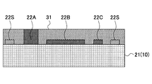
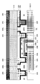
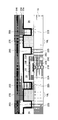
- FIG. 1 is a sectional view showing an example of an electronic component 20 according to the first embodiment
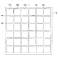
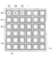
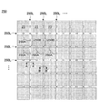
- FIG. 2 is a plan view showing a wafer 10 from which the electronic component 20 of FIG. 1 is cut out.
- the wafer 10 has, for example, a square planar shape, and on the wafer 10, a plurality of electronic component elements 10 ⁇ / b> A, 10 ⁇ / b> B, corresponding to the electronic components 20, respectively. 10C... Are separated by a scribe line 10L and formed in a matrix. 1 is obtained, for example, by dicing any one of the electronic component elements 10A, 10B, 10C,... Formed on the wafer 10 along the scribe line 10L. .
- the wafer is made of, for example, a low-temperature fired ceramic (LTCC) or the like, but can be made of glass, resin, a silicon substrate, or the like.
- LTCC low-temperature fired ceramic
- the electronic component 20 is a MEMS (micro-electromechanical system) switch, which is made of a low-temperature fired ceramic and is formed on a substrate 21 corresponding to the wafer 10.
- a MEMS (micro-electromechanical system) switch which is made of a low-temperature fired ceramic and is formed on a substrate 21 corresponding to the wafer 10.
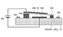
- a cantilever 23 carrying a contact 23A is formed at the tip portion via a support 22A made of copper (Cu) or the like.
- a contact 22C corresponding to the contact 23A is formed on the surface 21S of the substrate 21, and a drive electrode pattern 22B is formed for driving the cantilever 23 with electrostatic force.
- the contact 22C is actually composed of two contacts 22C 1 and 22C 2 , the cantilever 23 is attracted to the drive electrode pattern 22B, and the contact 23A is contacted with the contacts 22C 1 and 22C 1 . If contact with the 22C 2, for example, high-frequency signal incoming to the contact 22C 1 is output from the contact point 22C 2 conducts the contact 23A.
- the contact 22C includes the contacts 22C 1 and 22C 2 .
- the cantilever 23 is formed of, for example, a silicon oxide film, and carries an upper electrode pattern 23B thereon. Therefore, by applying a driving voltage between the driving electrode pattern 22B and the upper electrode pattern 23B, the cantilever 23 is generated between the driving electrode pattern 22B and the upper electrode pattern 23B. As a result, the contact 23A contacts or leaves the contact 22C.
- an electrode pattern 22D for supplying power to the upper electrode pattern 23B on the cantilever 23 through a bonding wire is formed on the surface 21S of the substrate 21.
- via plugs 21B and 21C are formed in the substrate 21 corresponding to the electrode patterns 22B and 22C, respectively. Although not shown in the cross section of FIG. 1, similar through via plugs are formed in the substrate 21 corresponding to the electrode patterns 22D.
- the through via plugs 21B and 21C, the support 22A, and the upper electrode pattern 23B are made of copper (Cu), for example, and the drive electrode pattern 22B and the contacts 22C and 23A are acid resistant such as gold (Au), for example. It is composed of a changeable metal.
- the support 22A, the electrode patterns 22B and 22D, the cantilever 23 and the contact 22C are continuously surrounded, and made of, for example, gold (Au) or gold / titanium (Au / A seal ring 22S having a Ti) laminated structure or a gold / chrome (Au / Cr) laminated structure is formed in an annular shape.
- a lid member 25 made of, for example, silicon and integrally including a side wall member 25S and a lid member 25C is disposed on the upper surface 21S of the substrate 21.
- the column 22A, the electrode patterns 22B to 22D, the cantilever 23, and the contact point 22C are placed so as to define an operation space 24 in which the contact point 22C is accommodated.
- the lid member 25 has an adhesion layer 25a of, for example, a gold / titanium or gold / chromium laminated structure formed on the entire upper surface thereof, ie, the surface opposite to the substrate 21.
- the side wall member 25S is bonded to the corresponding seal ring 22S via the adhesion layer 25a by placing the lid member 25 on the substrate 21. Further, a shield layer 26 made of, for example, iron-nickel alloy is bonded to the upper surface of the lid member 25.
- the outside of the side wall member 25S is filled with a space between the upper surface 21S of the substrate 21 and the lower surface 26S of the shield layer 26, and is in contact with the adhesion layer 25a covering the side wall surface of the side wall member 25S.
- a sealing member 27 made of tin-bismuth solder is formed.
- the side wall member 25S is further formed with a stepped portion made of a surface 25s facing the upper surface 21S of the substrate 21, and the sealing member 27 is only the side wall surface of the side wall member 25S of the lid member 25.
- the shield layer 26 and the lid member 25 are firmly bonded to the upper surface 21S of the substrate 21 by the sealing member 27.
- the sealing member 27 has a sidewall surface obtained by extending the sidewall surface 21SW of the substrate 21. Note that it is defined by 27SW.
- the sealing member 27 is formed outside the side wall member 25S when viewed from the working space 24.
- the sealing member 27 is bonded to the lid member 25 and the substrate 21, or the shield layer 26 and the substrate.
- the molten sealing member 27 does not flow into the working space 24 in order to promote the joining to the substrate 21.
- a close and strong joint can be realized directly between the seal ring 22S and the lid member 25 or via the sealing member 27, and the size of the working space 24 is made larger than necessary. A desirable feature that there is no need to set can be obtained.
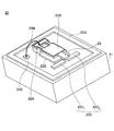
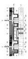
- FIG. 3 is a perspective view showing the main body of the MEMS switch 20 in more detail with the lid member 25, the shield layer 26, and the sealing member 27 removed.
- the electrode pattern 22D is formed on the upper surface 21S of the substrate 21 in the vicinity of the support 22A.
- the electrode pattern 22D is an upper electrode pattern 23B on the cantilever 23. It can be seen that they are connected by a bonding wire 23W. Further, as described above, through electrodes not shown corresponding to the electrode patterns 22D are formed in the substrate 21 in the same manner as the through electrode patterns 21B and 21C.
- the corresponds to the contact 22C has two contacts 22C 1 and 22C 2 is formed, a state where no driving voltage is applied between the electrode pattern 22B and 23B as shown in FIG. 4A in the two contacts 22C 1 and 22C 2 whereas in an electrically non-conductive, said state of Figure 4B where the DC drive voltage from the DC power supply 220 between the electrode pattern 22B and 23B is applied the contact 22C 1 and 22C 2 and conducted through the contact 23A, a high-frequency signal is output to the contact 22C 2, for example the incoming to an input terminal of the contact 22C 1.
- the seal ring 22S and the drive electrode pattern are formed on the surface 21S of the substrate 21 corresponding to the wafer 10.
- 22B and further contacts 22C 1 and 22C 2 are formed to a thickness of 1 ⁇ m, for example, by depositing and patterning a gold film, for example.
- the seal ring 22S is formed with a width of, for example, 150 ⁇ m along a scribe line 10L that defines an element region having a size of, for example, 1500 ⁇ m ⁇ 1000 ⁇ m, and is formed in the element region as described above.
- the pillars 22A, the electrode patterns 22B and 22D, and the contacts 22C 1 and 22C 2 are formed in an annular shape so as to continuously surround the structure.
- the seal ring 22S, the drive electrode pattern 22B, and the contacts 22C 1 and 22C 2 are not shown, but a thin gold film is formed as a seed layer on the surface of the substrate 21, that is, the wafer 10, and each of them is formed thereon.
- a resist film having a resist opening corresponding to the electrode pattern is formed, and the resist film can be formed by an electrolytic plating method using the resist film as a mask.
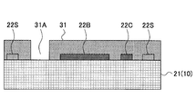
- a resist film 31 is formed on the substrate 21 so as to cover the structure on the surface 21S. Further, as shown in FIG. 5C, the resist film 31 corresponds to the support 22A. Thus, an opening 31A exposing the surface 21S is formed.
- the support 22A is formed to a height of 8 ⁇ m, for example, as shown in FIG.
- the gold film previously formed on the surface of the wafer 10 in the step of FIG. 5A can be used as a plating seed layer.
- an opening 31B for the contact 23A corresponding to the contacts 22C 1 and 22C 2 is formed to a predetermined depth of 2 ⁇ m, for example, as shown in FIG. 5E.
- a gold pattern filling the opening 31B is formed as the contact 23A to a thickness of 2 ⁇ m.
- the cantilever 23 is formed on the resist film 31 by, for example, a silicon oxide film having a thickness of 5 ⁇ m so as to extend from the support 22A to the contact 23A, and further on the cantilever 23.
- the upper electrode pattern 23B is formed by a copper pattern having a thickness of 0.5 ⁇ m, for example.
- the resist film 31 is dissolved in a solvent or removed by ashing in an oxygen atmosphere, and the upper electrode pattern 23B is not shown in the cross section of FIG. 5I.
- the MEMS switch 20 is formed by connecting the bonding wires 22W as described above with reference to FIG.
- the thin plating seed layer remaining on the surface of the wafer 10 in the step of FIG. 5A is removed by wet etching or the like. Since the plating seed layer is extremely thin, the structure formed in the element region is not substantially affected even when wet etching is performed in this way.
- the main body of the MEMS switch 20 shown in the perspective view of FIG. 3 is formed in all the element regions 10A, 10B, 10C... On the wafer 10 of FIG. It is formed.
- the MEMS switches 20 shown in the perspective view of FIG. 3 are formed in a matrix form on the wafer 10 and separated from each other by a scribe line 10L.
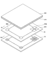
- a cap substrate 250 formed by joining the lid member 25 in a matrix corresponding to the element region on the wafer 10 is bonded onto the wafer 10 and further melted from above the cap substrate 250 to the lower surface.
- the shield substrate 260 carrying the sealant layer 270 such as solder is pressed.
- slit portions 250L corresponding to the scribe lines 10L on the wafer 10 are formed vertically and horizontally so as to surround the lid member 25, and the shield substrate 260 is formed on the cap substrate 250 from above.
- the sealant layer 270 flows under the cap substrate 250 from the slit portion 250L, and is a space between the plurality of MEMS switches 20 having the cross-sectional structure of FIG. Fill.
- FIG. 7 is a plan view showing the wafer 10 in the exploded perspective view of FIG.
- a body portion of the MEMS switch 20 shown in the perspective view of FIG. 3 is formed in the plurality of element regions 10A, 10B, 10C,.
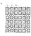
- FIG. 8A is a plan view of the cap substrate 250 in the exploded perspective view of FIG. 6 as viewed from the top, that is, the shield substrate 260 in FIG. 6, and FIG. 8B is the bottom of the cap substrate 250, that is, the wafer 10 in FIG. It is the top view seen from the side.
- the substrate 21 in FIG. 1 is formed by cutting the wafer 10 along the scribe line 10L.
- slits 250L extend vertically and horizontally corresponding to the scribe lines 10L of the wafer 10, and individual lid members 25 are defined.
- each lid member 25 is connected to the adjacent lid member 25 by a rib-like bridge portion 250A.
- Mechanically coupled by 250B the bridging portion 250A couples one lid member 25 to the lid member 25 adjacent in the row direction or the column direction, and the bridging portion 250B couples one lid member 25 to the lid member 25 adjacent in the oblique direction.
- the lower surface of the silicon substrate constituting the cap substrate 250 surrounds a recess corresponding to the working space 24 of FIG. It can be seen that it is formed in a ring shape in the form of a pattern.
- a method for manufacturing such a cap substrate 250 will be described later with reference to FIGS. 11A to 11D.
- FIGS. 9A to 9D are cross-sectional views along line AA ′ in FIG. 8A
- FIGS. 10A to 10D are cross-sectional views along line BB ′ in FIG. 8A.
- the adhesion layer 25a is formed on the lower surface of the cap substrate 250, and the side wall member 25S is disposed on the wafer 10 via the adhesion layer 25a.
- the side wall member 25S is disposed so as to contact the seal ring 22S and further presses the cap substrate 250 against the wafer 10 with a pressure of, for example, 1 MPa while being heated to a temperature of, for example, 280 ° C. Even if the seal ring 22S has some unevenness on the surfaces of the side wall member 25S and the seal ring 22S, the seal ring 22S is reliably bonded via the adhesion layer 25a.
- the working space 24 is defined. In the following description, only the working space 24 is illustrated for the element region adjacent to the element region, and the illustration of the MEMS switch 20 main body is omitted.
- a shield substrate 260 carrying a solder layer 270 on the lower surface is disposed on the structure of FIG. 9A.
- the solder layer 270 is melted in an inert atmosphere such as nitrogen, and the shield substrate 260 is pressed in the direction of the arrow, so that the molten solder layer 270 corresponds to the scribe line 10L from the slit 250L. It pushes out into the space 250V formed between each side wall member 25S and 25S between one element area and the adjacent element area.
- the space 250V is connected on the wafer 10, and the nitrogen gas filling the space 250V and excess molten solder pass through the space 250V and pass through the wafer 10.
- the space 250V is filled with the molten solder layer 270.
- the side wall member 25S is joined to the corresponding seal ring 22S in each element region.
- the working space 24 is filled with an inert gas such as nitrogen gas.
- an inert gas such as nitrogen gas.
- the wafer 10 is caused to act along the scribe line 10L, for example, the dicing blade 31 as indicated by an arrow, thereby causing the wafer 10 to move. Is divided into individual element regions, and the MEMS switch 20 described above with reference to FIG. 1 is obtained.
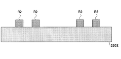
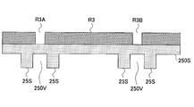
- 11A to 11D are process cross-sectional views illustrating a method for manufacturing the cap substrate 250.
- a resist pattern R1 corresponding to the side wall member 25S shown in the plan view of FIG. 8B is formed on a silicon substrate 250S formed in a square shape corresponding to the wafer 10.
- the silicon substrate 250S is etched to a predetermined depth corresponding to the height of the working space 24, for example, 50 ⁇ m, using the resist pattern R1 as a mask.
- the side wall member 25S is formed on the silicon substrate 250S, and the space 250V is formed between the side wall member 25S defining one element region and the side wall member 25S defining an adjacent element region. Is formed.
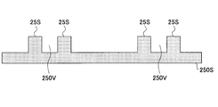
- the silicon substrate 250S in the state of FIG. 11B is turned upside down, and a resist pattern R3 having a resist opening R3A corresponding to the slit 250L is formed on the upper surface, and the resist pattern R3 is further formed.
- the slit 250L is formed in communication with the space 250V as shown in FIG. 11D.
- the process from the surface in which the space 250V is formed is also possible without turning the substrate 250S upside down.
- the silicon substrate 250S in the state of FIG. 11D is turned upside down, and the adhesion layer 25a is formed with a film thickness of, for example, 0.5 ⁇ m on the surface on which the side wall member 25S is formed.
- the cap substrate 250 is formed.
- the cap substrate 250 is formed of the silicon substrate 250S, and the lid member 25 is also formed of silicon. Accordingly, the present embodiment is not limited to such a specific material.
- the cap substrate 250 and the lid member 25 can be made of glass, metal, ceramic, or the like in addition to silicon.
- FIG. 12 is a cross-sectional view showing a configuration of a MEMS switch 20A according to a modification of the present embodiment.
- the same reference numerals are given to the portions corresponding to the previous embodiment, and the description will be omitted.
- a seal ring 32S having a height corresponding to the height of the working space 24 is formed by, for example, electrolytic plating of copper, and the like. Further, the working space 24 is defined by joining a flat lid member 35.
- the flat lid member 35 is made of, for example, silicon and has the same configuration as the lid member 35 made of silicon, but lacks the side wall portion 25S and has a flat lower surface.
- the adhesion layer 25a is formed on the lower surface and the side wall surface of the lid member 35, and the lid member 35 is disposed outside the seal ring 32S constituting the side wall member via a sealing member 27 such as solder.
- the substrate 21 is firmly bonded to the surface 21S.
- the shield layer 26 has an outer shape corresponding to the outer shape of the substrate 21, and the side wall surface defining the outer periphery of the lid member 35 is the side wall surface defining the outer periphery of the shield layer 26. 12 and the side wall surface defining the outer periphery of the seal ring 32S is formed at a position further retracted from the side wall surface of the lid member.
- Two step portions are formed as shown in FIG. In the embodiment of FIG. 12, both of the two stepped portions are filled with solder constituting the sealing portion 27, and as a result, the lid member 35 is firmly bonded to the surface of the substrate 21. .
- FIG. 12 uses a substrate having a flat bottom surface in which the side wall member 25S is not formed in the plan view of FIG. 8B as the cap substrate 250 in the wafer level packaging described with reference to FIG. 9A to 9D and FIGS. 10A to 10D can be formed in the same manner.
- FIG. 13 is a cross-sectional view showing a configuration of a MEMS switch 20B according to another modification of the present embodiment.
- portions corresponding to the previous embodiment are denoted by the same reference numerals, and description thereof is omitted.
- the side wall surface defining the outer periphery of the lid member 35 is the side wall member 32S that also serves as the side wall surface defining the outer periphery of the shield layer 26 that coincides with the outer periphery of the substrate 21 and the seal ring. It should be noted that it is formed at a position that is recessed from any of the side wall surfaces that define the outer periphery.
- a stepped portion filled with the sealing member 27 is formed as shown in the figure, and the shield layer 26 is formed on the substrate 21 by the sealing member 27. Tightly coupled.
- the lid member 35 is firmly coupled to the substrate 11.
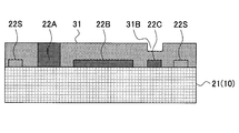
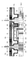
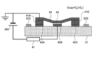
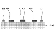
- FIG. 14 is a cross-sectional view showing the configuration of the variable capacitance element 40 according to the second embodiment
- FIG. 15 is a perspective view showing the configuration of the main body of the variable capacitance element 40 of FIG.
- the cross-sectional view of FIG. 14 shows a cross section taken along line CC ′ in the perspective view of FIG.
- portions corresponding to the portions described above are denoted by the same reference numerals, and description thereof is omitted.
- a ground electrode pattern made of gold instead of the support 22A and the electrode pattern 22C on the substrate 21 corresponding to one element region of the wafer 10.
- 42A and 42C are formed, respectively, and pillars 41A and 41C made of copper are formed on the ground electrode patterns 42A and 42C, for example, at a height of 2 ⁇ m.
- An upper electrode pattern 42 of an air bridge structure made of a gold film is formed between the support posts 41A and 41C with a film thickness of, for example, 1 ⁇ m.
- a lower electrode pattern 42B is formed to face the upper electrode 42.
- the upper electrode pattern 42 is provided so as to be displaceable with respect to the opposed lower electrode pattern 42B, and the upper electrode pattern 42 and the lower electrode pattern 42B constitute a variable capacitance element.
- a capacitor dielectric film 43 made of a silicon oxide film or the like is formed on the lower electrode pattern 42B so that the upper electrode pattern 42 and the lower electrode pattern 42B are not short-circuited.
- the seal ring 22S defines an element region on the substrate 21 as in the previous embodiment, and the lower electrode pattern 42B is on the surface 21S of the substrate 21. It can be seen that it extends under the upper electrode pattern 42 from the high frequency signal input side (RFin) to the high frequency signal output side (RFout). Also in the substrate 21, the via plug 21B 1 and 21B 2 shown in cross section in FIG. 14, it is formed to correspond to and the output side to each of the input side.
- the seal ring 22S and the electrode patterns 42A and 42C are grounded via through via plugs 21A and 21C formed in the substrate 21, respectively (GND).
- the variable capacitance element 40 is connected to a high-frequency transmission path formed by the lower electrode pattern 42B by a capacitance Ccap formed between the upper electrode pattern 42 and the lower electrode pattern 42B. An element having the above structure is formed.
- FIG. 16A and 16B are diagrams for explaining the operation of the variable capacitance element 40.
- FIG. 16A and 16B are diagrams for explaining the operation of the variable capacitance element 40.
- variable capacitance element 40 by applying a DC voltage between the upper electrode 42 and the lower electrode 42B, the lower electrode pattern 42B is formed as shown in the equivalent circuit diagram of FIG. 16C.
- the capacitance of the capacitor connected to the transmission path of the high frequency signal to be configured can be changed.
- the adhesion layer 25 a having an Au / Ti laminated structure is removed from the portion of the lid member 25 facing the substrate 21 in the working space 24. It should be noted that. According to this configuration, no parasitic capacitance is generated between the electrode pattern to which a high frequency signal is supplied on the substrate 21 and the lid member 25, and the influence of the parasitic capacitance on the operation of the variable capacitance element 40 is suppressed. can do.
- variable capacitance element 40 of FIG. 14 will be described.
- the seal ring 22S and the ground electrode pattern are formed on the surface 21S of the substrate 21 corresponding to the wafer 10.
- 42A, 42C and the lower electrode pattern 42B are formed to a thickness of 1 ⁇ m, for example, by depositing and patterning a gold film, for example.
- the seal ring 22S is formed with a width of, for example, 150 ⁇ m along the scribe line 10L that defines an element region having a dimension of, for example, 1500 ⁇ m ⁇ 1000 ⁇ m.
- the electrode patterns 42A to 42C and the like formed in the element region are formed in an annular shape so as to continuously surround the structure.
- a thin gold film that is not shown in the drawing and serves as a plating seed layer is formed on the surface 21S of the substrate 21, and thus on the surface of the wafer 10.
- the seal ring 22S and the electrode patterns 42A to 42C are formed by electrolytic plating using a resist pattern formed on the plating seed layer and having a resist opening corresponding to each of the electrode patterns 42A to 42C as a mask.
- a dielectric film such as a silicon oxide film is formed on the substrate 21 and further patterned by a resist process (not shown), thereby forming the dielectric film on the lower electrode pattern 42B as shown in FIG. 17B.
- a capacitor insulating film 43 made of, for example, a silicon oxide film is formed.
- a resist film 45 is formed on the substrate 21 so as to cover the seal ring 22S and the electrode patterns 42A to 42C, and further, the ground electrode is formed in the resist film 45 as shown in FIG. 17D.
- openings 45A and 45C are formed so as to expose the ground electrode patterns 42A and 42C.
- a copper film is formed on the ground electrode patterns 42A and 42C so as to fill the resist openings 45A and 45C.
- a support post 41A made of copper and a support post 41C made of copper are formed on the ground electrode pattern 42C by electrolytic plating.
- the gold film previously formed on the surface of the wafer 10 in the step of FIG. 17A can be used as a plating seed layer.
- a gold film is formed on the resist film 45 by a low temperature process such as sputtering, and further patterned to form an upper electrode pattern 42 that bridges the support columns 41A and 41C.
- the resist film 45 is dissolved in a solvent or the like, or is removed by ashing in an oxygen atmosphere, whereby the variable capacitance element 40 of FIG. 14 is formed.
- the seal ring 22S, the electrode patterns 22B, 22C, etc. are formed by the electrolytic plating method in the process of FIG. 17A, the plating seed layer remaining on the surface of the wafer 10 is After the resist film 45 is removed, the resist film 45 is removed by wet etching or the like.
- variable capacitance element 40 is formed in each of the element regions 10A, 10B, 10C,..., FIGS. 6, 7, 8A to 8B, and 9A to 9D are previously described.
- the variable capacitance element 40 shown in FIG. 14 is completed.
- the adhesive layer 25a is removed from the lower surface of the lid member 25 made of silicon in order to reduce parasitic capacitance. Should.
- the process of FIGS. 18A and 18B is further performed following the process of FIG.
- the adhesion layer 25 a is removed from the portion of the substrate 250 that faces the surface 21 ⁇ / b> S of the substrate 21 when the lid member 25 is mounted on the substrate 21.
- a resist pattern R4 is formed on the silicon substrate 250S constituting the cap substrate 250 so as to cover the slit portion 250L and the side wall member 25S, and further, the silicon substrate using the resist pattern R4 as a mask.
- the adhesion layer 25a exposed on 250S is removed by, for example, sputter etching or wet etching.
- variable capacitor 40 having the structure described above with reference to FIG. 14 can be obtained.
- the lid member 25, and thus the cap substrate 250 is not limited to silicon, but can be formed of an insulating material such as glass or ceramic.
- the lid member 25, and hence the cap substrate 250 is formed of silicon, it is preferable to use an insulating silicon substrate having a specific resistance of 1000 ⁇ cm or more.
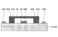
- FIG. 19 is a cross-sectional view showing a configuration of a variable capacitor 40A according to a modification of the present embodiment.
- the same reference numerals are assigned to portions corresponding to the previous embodiment, and the description thereof is omitted.
- a seal ring 32 ⁇ / b> S having a height corresponding to the height of the working space 24 is replaced with, for example, copper.
- the working space 24 is defined by joining a flat lid member 35 thereon.
- the flat lid member 35 is made of, for example, silicon and has the same configuration as the lid member 35 made of silicon, but lacks the side wall portion 25S and has a flat lower surface.
- the adhesion layer 25a is formed on the lower surface and the side wall surface of the lid member 35, and the lid member 35 is disposed outside the seal ring 32S constituting the side wall member via a sealing member 27 such as solder.
- the substrate 21 is firmly bonded to the surface 21S.
- the shield layer 26 has an outer shape corresponding to the outer shape of the substrate 21, and the side wall surface defining the outer periphery of the lid member 35 is the side wall surface defining the outer periphery of the shield layer 26. 19 and the side wall surface defining the outer periphery of the seal ring 32S is formed at a position further retracted from the side wall surface of the lid member.
- Two step portions are formed as shown in FIG. In the embodiment of FIG. 19, both of the two stepped portions are filled with solder constituting the sealing portion 27, and as a result, the lid member 35 is firmly bonded to the surface of the substrate 21. .
- FIG. 19 uses a substrate having a flat bottom surface in which the side wall member 25S is not formed in the plan view of FIG. 8B as the cap substrate 250 in the wafer level packaging described with reference to FIG. 9A to 9D and FIGS. 10A to 10D can be formed in the same manner.
- FIG. 20 is a cross-sectional view showing a configuration of a variable capacitor 40B according to another modification of the present embodiment.
- parts corresponding to those of the previous embodiment are denoted by the same reference numerals, and description thereof is omitted.
- the side wall surface that defines the outer periphery of the lid member 35 is the side wall member 32 ⁇ / b> S that also functions as the side wall surface that defines the outer periphery of the shield layer 26 that coincides with the outer periphery of the substrate 21. It should be noted that it is formed at a position that is recessed from any of the side wall surfaces that define the outer periphery.
- a stepped portion filled with the sealing member 27 is formed as shown in the figure, and the shield layer 26 is formed on the substrate 21 by the sealing member 27. Tightly coupled.
- the lid member 35 is firmly coupled to the substrate 11.
- the size of the lid member 35 is reduced, and the variable capacitance element 40B can be further downsized.
- the sealing member 27 is not limited to solder, and for example, a resin can be used. By using a resin as the sealing member 27, the electronic component can be reduced in weight.
- the element formed in the working space 24 is not limited to a MEMS switch or a variable capacitance element, and it is also possible to form a crystal resonator, for example.
Abstract
La présente invention porte sur un composant électronique qui comporte : un substrat ; un élément qui est formé sur le substrat ; un élément de paroi latérale qui entoure l'élément sur le substrat ; un élément de couverture qui est agencé sur l'élément de paroi latérale et forme un espace, qui entoure l'élément au-dessus du substrat, conjointement avec l'élément de paroi latérale ; et un élément d'étanchéité qui est agencé à l'extérieur de l'élément de paroi latérale et lie l'élément de paroi latérale et l'élément de couverture à la surface du substrat, scellant ainsi l'espace.
Priority Applications (4)
| Application Number | Priority Date | Filing Date | Title |
|---|---|---|---|
| PCT/JP2011/076962 WO2013076830A1 (fr) | 2011-11-22 | 2011-11-22 | Composant électronique et procédé de production de celui-ci |
| JP2013545705A JP5842929B2 (ja) | 2011-11-22 | 2011-11-22 | 電子部品およびその製造方法 |
| CN201180074343.7A CN103890932B (zh) | 2011-11-22 | 2011-11-22 | 电子部件及其制造方法 |
| US14/251,004 US9343382B2 (en) | 2011-11-22 | 2014-04-11 | Electronic device and manufacturing method thereof |
Applications Claiming Priority (1)
| Application Number | Priority Date | Filing Date | Title |
|---|---|---|---|
| PCT/JP2011/076962 WO2013076830A1 (fr) | 2011-11-22 | 2011-11-22 | Composant électronique et procédé de production de celui-ci |
Related Child Applications (1)
| Application Number | Title | Priority Date | Filing Date |
|---|---|---|---|
| US14/251,004 Continuation US9343382B2 (en) | 2011-11-22 | 2014-04-11 | Electronic device and manufacturing method thereof |
Publications (1)
| Publication Number | Publication Date |
|---|---|
| WO2013076830A1 true WO2013076830A1 (fr) | 2013-05-30 |
Family
ID=48469309
Family Applications (1)
| Application Number | Title | Priority Date | Filing Date |
|---|---|---|---|
| PCT/JP2011/076962 WO2013076830A1 (fr) | 2011-11-22 | 2011-11-22 | Composant électronique et procédé de production de celui-ci |
Country Status (4)
| Country | Link |
|---|---|
| US (1) | US9343382B2 (fr) |
| JP (1) | JP5842929B2 (fr) |
| CN (1) | CN103890932B (fr) |
| WO (1) | WO2013076830A1 (fr) |
Cited By (4)
| Publication number | Priority date | Publication date | Assignee | Title |
|---|---|---|---|---|
| JP2015130394A (ja) * | 2014-01-07 | 2015-07-16 | 株式会社デンソー | モールドパッケージ |
| JP2019169703A (ja) * | 2018-03-23 | 2019-10-03 | 日本ケミコン株式会社 | バスバー積層体及びそれを備える電子部品実装モジュール、バスバー積層体の製造方法 |
| US11539346B2 (en) | 2019-01-31 | 2022-12-27 | Seiko Epson Corporation | Resonator device, resonator module, electronic apparatus, and vehicle |
| US11575361B2 (en) | 2019-01-31 | 2023-02-07 | Seiko Epson Corporation | Resonator device, resonator module, electronic apparatus, and vehicle |
Families Citing this family (7)
| Publication number | Priority date | Publication date | Assignee | Title |
|---|---|---|---|---|
| US9560781B2 (en) * | 2013-07-19 | 2017-01-31 | Materion Corporation | Metal cap assembly for optical communications |
| CN105765716B (zh) * | 2014-05-15 | 2018-06-22 | 富士电机株式会社 | 功率半导体模块和复合模块 |
| CN104900540B (zh) * | 2015-06-17 | 2018-04-06 | 上海集成电路研发中心有限公司 | 一种晶圆级真空封装的mems晶振及其制备方法 |
| KR101658033B1 (ko) * | 2015-07-10 | 2016-09-30 | 룩씨스 주식회사 | 칩형 전자부품의 하드코팅 제조방법 |
| CN106711121B (zh) * | 2015-11-12 | 2019-09-06 | 中国科学院上海微系统与信息技术研究所 | 一种硅柱通孔互连结构及其制作方法 |
| CN105826275B (zh) * | 2016-03-21 | 2018-10-26 | 中国电子科技集团公司第五十五研究所 | 硅基多通道tr组件及设计方法 |
| WO2019181846A1 (fr) * | 2018-03-23 | 2019-09-26 | 日本ケミコン株式会社 | Corps stratifié de barre omnibus, module de montage de composant électronique pourvu de celui-ci, et procédé de fabrication de corps stratifié de barre omnibus |
Citations (5)
| Publication number | Priority date | Publication date | Assignee | Title |
|---|---|---|---|---|
| JPH11150201A (ja) * | 1997-11-18 | 1999-06-02 | Kyocera Corp | 電子部品収納用パッケージ |
| JP2002231919A (ja) * | 2001-02-06 | 2002-08-16 | Olympus Optical Co Ltd | 固体撮像装置及びその製造方法 |
| JP2006013330A (ja) * | 2004-06-29 | 2006-01-12 | Shinko Electric Ind Co Ltd | 貫通電極及びその製造方法 |
| JP2007013573A (ja) * | 2005-06-30 | 2007-01-18 | Kyocera Kinseki Corp | 圧電デバイスの製造方法 |
| JP2009107041A (ja) * | 2007-10-29 | 2009-05-21 | Nippon Telegr & Teleph Corp <Ntt> | 微細構造体及びその製造方法 |
Family Cites Families (9)
| Publication number | Priority date | Publication date | Assignee | Title |
|---|---|---|---|---|
| JPH11340350A (ja) | 1998-05-27 | 1999-12-10 | Kyocera Corp | 電子装置用容器およびその封止方法 |
| US6777263B1 (en) * | 2003-08-21 | 2004-08-17 | Agilent Technologies, Inc. | Film deposition to enhance sealing yield of microcap wafer-level package with vias |
| JP2006074291A (ja) | 2004-08-31 | 2006-03-16 | Kyocera Kinseki Corp | 電子装置の製造方法 |
| US20090212657A1 (en) * | 2005-02-07 | 2009-08-27 | National University Corporation Saitama University | Equivalent-capacitance type actuator drive device |
| US20070190747A1 (en) * | 2006-01-23 | 2007-08-16 | Tessera Technologies Hungary Kft. | Wafer level packaging to lidded chips |
| US20080142946A1 (en) * | 2006-12-13 | 2008-06-19 | Advanced Chip Engineering Technology Inc. | Wafer level package with good cte performance |
| JP5540911B2 (ja) * | 2010-06-09 | 2014-07-02 | 三菱電機株式会社 | 半導体装置 |
| US8754529B2 (en) * | 2011-03-28 | 2014-06-17 | Miradia, Inc. | MEMS device with simplified electrical conducting paths |
| US8604576B2 (en) * | 2011-07-19 | 2013-12-10 | Opitz, Inc. | Low stress cavity package for back side illuminated image sensor, and method of making same |
-
2011
- 2011-11-22 JP JP2013545705A patent/JP5842929B2/ja not_active Expired - Fee Related
- 2011-11-22 CN CN201180074343.7A patent/CN103890932B/zh not_active Expired - Fee Related
- 2011-11-22 WO PCT/JP2011/076962 patent/WO2013076830A1/fr active Application Filing
-
2014
- 2014-04-11 US US14/251,004 patent/US9343382B2/en not_active Expired - Fee Related
Patent Citations (5)
| Publication number | Priority date | Publication date | Assignee | Title |
|---|---|---|---|---|
| JPH11150201A (ja) * | 1997-11-18 | 1999-06-02 | Kyocera Corp | 電子部品収納用パッケージ |
| JP2002231919A (ja) * | 2001-02-06 | 2002-08-16 | Olympus Optical Co Ltd | 固体撮像装置及びその製造方法 |
| JP2006013330A (ja) * | 2004-06-29 | 2006-01-12 | Shinko Electric Ind Co Ltd | 貫通電極及びその製造方法 |
| JP2007013573A (ja) * | 2005-06-30 | 2007-01-18 | Kyocera Kinseki Corp | 圧電デバイスの製造方法 |
| JP2009107041A (ja) * | 2007-10-29 | 2009-05-21 | Nippon Telegr & Teleph Corp <Ntt> | 微細構造体及びその製造方法 |
Cited By (5)
| Publication number | Priority date | Publication date | Assignee | Title |
|---|---|---|---|---|
| JP2015130394A (ja) * | 2014-01-07 | 2015-07-16 | 株式会社デンソー | モールドパッケージ |
| JP2019169703A (ja) * | 2018-03-23 | 2019-10-03 | 日本ケミコン株式会社 | バスバー積層体及びそれを備える電子部品実装モジュール、バスバー積層体の製造方法 |
| JP7199639B2 (ja) | 2018-03-23 | 2023-01-06 | 日本ケミコン株式会社 | バスバー積層体及びそれを備える電子部品実装モジュール、バスバー積層体の製造方法 |
| US11539346B2 (en) | 2019-01-31 | 2022-12-27 | Seiko Epson Corporation | Resonator device, resonator module, electronic apparatus, and vehicle |
| US11575361B2 (en) | 2019-01-31 | 2023-02-07 | Seiko Epson Corporation | Resonator device, resonator module, electronic apparatus, and vehicle |
Also Published As
| Publication number | Publication date |
|---|---|
| US9343382B2 (en) | 2016-05-17 |
| CN103890932B (zh) | 2017-03-29 |
| US20140203424A1 (en) | 2014-07-24 |
| CN103890932A (zh) | 2014-06-25 |
| JPWO2013076830A1 (ja) | 2015-04-27 |
| JP5842929B2 (ja) | 2016-01-13 |
Similar Documents
| Publication | Publication Date | Title |
|---|---|---|
| JP5842929B2 (ja) | 電子部品およびその製造方法 | |
| JP4312631B2 (ja) | ウエハレベルパッケージ構造体とその製造方法、及びそのウエハレベルパッケージ構造体から分割された素子 | |
| JP5026038B2 (ja) | 電子部品装置 | |
| US6384353B1 (en) | Micro-electromechanical system device | |
| US7696004B2 (en) | Wafer level package fabrication method | |
| CN104051408A (zh) | 模块及其制造方法 | |
| JP2001196488A (ja) | 電子部品装置及びその製造方法 | |
| KR20110054710A (ko) | 소자 패키지 및 그 제조 방법 | |
| US20110114355A1 (en) | Hermetically sealed housing for electronic components and manufacturing method | |
| WO2005104616A1 (fr) | Microphone a condensateur a electret | |
| KR100558439B1 (ko) | 웨이퍼 레벨 패키지의 fbar 소자 및 그 제조 방법 | |
| JP4403977B2 (ja) | 機能素子体及びその製造方法並びに回路モジュール | |
| US20080018415A1 (en) | Surface acoustic wave device | |
| JP5465002B2 (ja) | 蓋部材ウエハの製造方法及び蓋部材の製造方法 | |
| JP2007042786A (ja) | マイクロデバイス及びそのパッケージング方法 | |
| JP2008034515A (ja) | 電子装置およびパッケージ | |
| JP4268480B2 (ja) | 電子部品封止用基板およびそれを用いた電子装置 | |
| JP2005262382A (ja) | 電子装置およびその製造方法 | |
| JP4761713B2 (ja) | 電子部品封止用基板および多数個取り用電子部品封止用基板ならびに電子装置の製造方法 | |
| JP6675181B2 (ja) | トランスデューサ装置及びその製造方法 | |
| JP2016006946A (ja) | 水晶デバイスの製造方法 | |
| JP2003133452A (ja) | 電子装置の製造方法 | |
| JP4434870B2 (ja) | 多数個取り電子部品封止用基板および電子装置ならびに電子装置の製造方法 | |
| JP2005212016A (ja) | 電子部品封止用基板および多数個取り用電子部品封止用基板ならびに電子装置の製造方法 | |
| JP4780700B2 (ja) | 素子保護用電子部品およびその製造方法 |
Legal Events
| Date | Code | Title | Description |
|---|---|---|---|
| 121 | Ep: the epo has been informed by wipo that ep was designated in this application |
Ref document number: 11876311 Country of ref document: EP Kind code of ref document: A1 |
|
| ENP | Entry into the national phase |
Ref document number: 2013545705 Country of ref document: JP Kind code of ref document: A |
|
| NENP | Non-entry into the national phase |
Ref country code: DE |
|
| 122 | Ep: pct application non-entry in european phase |
Ref document number: 11876311 Country of ref document: EP Kind code of ref document: A1 |