WO2013073080A1 - 光源装置及び波長変換方法 - Google Patents
光源装置及び波長変換方法 Download PDFInfo
- Publication number
- WO2013073080A1 WO2013073080A1 PCT/JP2012/005205 JP2012005205W WO2013073080A1 WO 2013073080 A1 WO2013073080 A1 WO 2013073080A1 JP 2012005205 W JP2012005205 W JP 2012005205W WO 2013073080 A1 WO2013073080 A1 WO 2013073080A1
- Authority
- WO
- WIPO (PCT)
- Prior art keywords
- output
- light
- temperature control
- light source
- source device
- Prior art date
- Legal status (The legal status is an assumption and is not a legal conclusion. Google has not performed a legal analysis and makes no representation as to the accuracy of the status listed.)
- Ceased
Links
Images




Classifications
-
- G—PHYSICS
- G02—OPTICS
- G02F—OPTICAL DEVICES OR ARRANGEMENTS FOR THE CONTROL OF LIGHT BY MODIFICATION OF THE OPTICAL PROPERTIES OF THE MEDIA OF THE ELEMENTS INVOLVED THEREIN; NON-LINEAR OPTICS; FREQUENCY-CHANGING OF LIGHT; OPTICAL LOGIC ELEMENTS; OPTICAL ANALOGUE/DIGITAL CONVERTERS
- G02F1/00—Devices or arrangements for the control of the intensity, colour, phase, polarisation or direction of light arriving from an independent light source, e.g. switching, gating or modulating; Non-linear optics
- G02F1/01—Devices or arrangements for the control of the intensity, colour, phase, polarisation or direction of light arriving from an independent light source, e.g. switching, gating or modulating; Non-linear optics for the control of the intensity, phase, polarisation or colour
- G02F1/0147—Devices or arrangements for the control of the intensity, colour, phase, polarisation or direction of light arriving from an independent light source, e.g. switching, gating or modulating; Non-linear optics for the control of the intensity, phase, polarisation or colour based on thermo-optic effects
-
- G—PHYSICS
- G02—OPTICS
- G02F—OPTICAL DEVICES OR ARRANGEMENTS FOR THE CONTROL OF LIGHT BY MODIFICATION OF THE OPTICAL PROPERTIES OF THE MEDIA OF THE ELEMENTS INVOLVED THEREIN; NON-LINEAR OPTICS; FREQUENCY-CHANGING OF LIGHT; OPTICAL LOGIC ELEMENTS; OPTICAL ANALOGUE/DIGITAL CONVERTERS
- G02F1/00—Devices or arrangements for the control of the intensity, colour, phase, polarisation or direction of light arriving from an independent light source, e.g. switching, gating or modulating; Non-linear optics
- G02F1/35—Non-linear optics
- G02F1/37—Non-linear optics for second-harmonic generation
- G02F1/377—Non-linear optics for second-harmonic generation in an optical waveguide structure
- G02F1/3775—Non-linear optics for second-harmonic generation in an optical waveguide structure with a periodic structure, e.g. domain inversion, for quasi-phase-matching [QPM]
-
- G—PHYSICS
- G02—OPTICS
- G02F—OPTICAL DEVICES OR ARRANGEMENTS FOR THE CONTROL OF LIGHT BY MODIFICATION OF THE OPTICAL PROPERTIES OF THE MEDIA OF THE ELEMENTS INVOLVED THEREIN; NON-LINEAR OPTICS; FREQUENCY-CHANGING OF LIGHT; OPTICAL LOGIC ELEMENTS; OPTICAL ANALOGUE/DIGITAL CONVERTERS
- G02F1/00—Devices or arrangements for the control of the intensity, colour, phase, polarisation or direction of light arriving from an independent light source, e.g. switching, gating or modulating; Non-linear optics
- G02F1/35—Non-linear optics
- G02F1/353—Frequency conversion, i.e. wherein a light beam is generated with frequency components different from those of the incident light beams
- G02F1/3544—Particular phase matching techniques
- G02F1/3546—Active phase matching, e.g. by electro- or thermo-optic tuning
Definitions
- the present invention relates to a light source device provided with a waveguide having a polarization inversion structure and a wavelength conversion method.
- the quasi phase matching is performed using an element in which a polarization inversion structure is periodically formed in a ferroelectric crystal.
- Patent Document 1 describes that a thin film heater is provided in a waveguide having a polarization inversion structure.
- Patent Document 2 describes that a plurality of temperature control elements are provided along a waveguide having a polarization inversion structure.
- a Peltier element is used as a temperature control element.
- Heaters and Peltier elements have long time constants. For this reason, when temperature control of the polarization inversion structure is performed using a heater or a Peltier element, it takes time to bring the polarization inversion structure to a desired temperature.
- the present invention has been made in view of the above circumstances, and an object of the present invention is to provide a light source device and a wavelength conversion method in which the time taken to bring the polarization inversion structure to a desired temperature is short.
- a light source device includes a ferroelectric crystal, an output light incident unit, a temperature control light irradiation unit, and a control unit.
- the ferroelectric crystal has a light input portion, a light output portion, and a polarization inversion structure.
- a polarization inversion structure is provided between the input and the output.
- the output light incident portion inputs the output light to the input portion of the ferroelectric crystal.
- the output light is wavelength converted by the polarization inversion structure of the ferroelectric crystal.
- the temperature control light irradiation unit irradiates the temperature control light to the polarization inversion structure of the ferroelectric crystal.
- the temperature control light has a wavelength that is absorbed by the ferroelectric crystal.
- the control unit controls the output of the temperature control light.
- the wavelength conversion method irradiates temperature control light, which is light of a wavelength absorbed by the ferroelectric crystal, on the polarization inversion structure provided between the light input and output parts of the ferroelectric crystal. Do. Thereby, the temperature of the polarization inversion structure is controlled. Then, the output light wavelength-converted by the polarization inversion structure is input to the input portion of the ferroelectric crystal, and the output light wavelength-converted by the polarization inversion structure is output from the output portion of the ferroelectric crystal.
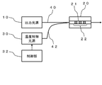
- FIG. 1 is a view showing the configuration of a light source device according to the first embodiment.
- the light source device includes a ferroelectric crystal 20, an output light source 10, a temperature control light source 30, and a control unit 32.
- the ferroelectric crystal 20 is, for example, LiNbO 3 doped with Mg, but is not limited thereto.
- the ferroelectric crystal 20 has an input portion and an output portion of light.
- the waveguide 21 is formed in the ferroelectric crystal 20.
- the structure of the waveguide 21 is not limited.
- the waveguide 21 may be, for example, a ridge structure or an embedded type.
- One end of the waveguide 21 is an input portion of light, and the other end is an output portion of light.
- the polarization inversion structure 22 is provided in the waveguide 21. The period of polarization inversion of the polarization inversion structure 22 is determined based on the wavelength of light output from the output light source 10.
- the output light source 10 is coupled to the input end of the waveguide 21 through an optical fiber 40.
- the output light source 10 injects output light into the waveguide 21.
- the output light has a wavelength whose wavelength is converted by the polarization inversion structure 22 of the waveguide 21. That is, the output light of the output light source 10 is wavelength-converted by the polarization inversion structure 22 of the waveguide 21 and then emitted from the output side end of the waveguide 21.
- the temperature control light source 30 irradiates the polarization control structure 22 of the waveguide 21 with temperature control light.
- the temperature control light has a wavelength absorbed by the ferroelectric crystal 20.
- the temperature control light preferably has an absorptivity of 10% or more and 90% or less in the ferroelectric crystal 20.
- the wavelength of the temperature control light is shorter than, for example, the absorption edge of the absorption region on the short wavelength side of the ferroelectric crystal 20, or longer than the absorption edge of the absorption region on the long wavelength side of the ferroelectric crystal 20.
- the wavelength of the temperature control light is, for example, 300 nm or less, or 4.5 ⁇ m or more.
- the temperature control light source 30 has temperature control light incident on the input side end of the waveguide 21. Specifically, the temperature control light source 30 outputs temperature control light to the optical fiber 42.
- the optical fiber 42 is connected to the optical fiber 40 via a multiplexer 50 (for example, a coupler). Therefore, the temperature control light incident on the optical fiber 42 is input to the input side end of the waveguide 21 through the multiplexing unit 50 and the optical fiber 40.
- the ferroelectric crystal 20 may be used in bulk without forming a waveguide in the ferroelectric crystal 20. Further, in the temperature control light source 30, the wavelength of the light to be emitted may be fixed or variable. In the example shown in the figure, only one temperature control light source 30 is provided. However, a plurality of temperature control light sources 30 that emit light of different wavelengths may be provided.
- optical path between the output light source 10 and the ferroelectric crystal 20 may be formed by a lens or a mirror instead of the optical fiber 40.
- optical path between the temperature control light source 30 and the ferroelectric crystal 20 may be formed not by the optical fiber 42 but by a lens or a mirror.
- the controller 32 controls the output of the temperature control light source 30.
- the temperature control light source 30 irradiates the polarization inversion structure 22 with temperature control light.
- the temperature control light has a wavelength that is absorbed by the ferroelectric crystal 20. Therefore, by controlling the output of the temperature control light source 30, the temperature of the polarization inversion structure 22 can be controlled.
- the controllability of the output of the temperature control light source 30 is high. Therefore, compared with the case where temperature control is performed only with a heater or a Peltier element, the time for the polarization inversion structure 22 to reach a desired temperature is shortened.
- the temperature control light is incident from the input side end of the waveguide 21. Therefore, the polarization inversion structure 22 can be locally heated. Therefore, the time for the polarization inversion structure 22 to reach the desired temperature is further shortened.
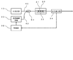
- FIG. 2 is a view showing the configuration of a light source device according to the second embodiment.
- This light source device has the same configuration as the light source device according to the first embodiment except that the optical fiber 42 is directly connected to the ferroelectric crystal 20. Also according to this embodiment, the same effect as that of the first embodiment can be obtained.
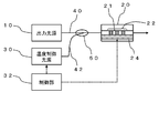
- FIG. 3 is a view showing the configuration of a light source device according to a third embodiment.
- This light source device has the same configuration as the light source device according to the first embodiment except that the temperature control light source 30 irradiates the temperature control light to the side portion of the polarization inversion structure 22. Also according to this embodiment, the same effect as that of the first embodiment can be obtained.
- FIG. 4 is a view showing the configuration of the light source device according to the fourth embodiment.
- This light source device has the same configuration as the light source device shown in any of the first to third embodiments except that it has the output detection unit 34. This figure shows the same case as the first embodiment.
- the output detection unit 34 detects the intensity of the output light output from the output side end of the waveguide 21.
- the detection result by the output detection unit 34 is transmitted to the control unit 32.
- the control unit 32 controls the output of the temperature control light source 30 based on the detection result received from the output detection unit 34. Specifically, the control unit 32 controls the output of the temperature control light source 30 such that the intensity detected by the output detection unit 34 is maximized.
- part of the output light output from the ferroelectric crystal 20 may be branched by using the branch part 52 and may be input to the output detection unit 34. In this way, the influence of the output detection unit 34 on the output of the ferroelectric crystal 20 can be reduced.
- control unit 32 controls the output of the temperature control light source 30 based on the detection result received from the output detection unit 34. Therefore, temperature control of the polarization inversion structure 22 can be easily performed.
- FIG. 6 is a view showing the configuration of a light source device according to the fifth embodiment.
- This light source device has the same configuration as the light source device shown in any of the first to third embodiments, except that the light source device has the temperature detection unit. This figure shows the same case as the first embodiment.
- the temperature detection unit 36 detects the temperature of the polarization inversion structure 22.
- the detection result of the temperature detection unit 36 is transmitted to the control unit 32.
- the control unit 32 controls the output of the temperature control light source 30 based on the detection result received from the temperature detection unit 36. Specifically, the control unit 32 controls the output of the temperature control light source 30 so that the temperature detected by the temperature detection unit 36 becomes a predetermined value.
- control unit 32 controls the output of the temperature control light source 30 based on the detection result received from the temperature detection unit 36. Therefore, temperature control of the polarization inversion structure 22 can be easily performed.
- FIG. 7 is a view showing a configuration of a light source device according to a sixth embodiment.
- This light source device has the same configuration as the light source device shown in any of the first to fifth embodiments except that the light source device has the temperature control element 24. This figure shows the same case as the first embodiment.
- the temperature control element 24 is attached in the vicinity of the waveguide 21 in the ferroelectric crystal 20, and performs at least one of heat generation and heat absorption.
- the temperature control element 24 is, for example, a heater or a Peltier element.
- the temperature control element 24 is controlled by the control unit 32.
- the control unit 32 uses the temperature control element 24 as a main temperature control mechanism, and uses the temperature control light source 30 as a sub temperature control mechanism. Specifically, the temperature control element 24 is used to control the temperature of the polarization inversion structure 22 to some extent, and the temperature control light source 30 is used to finely adjust the temperature of the polarization inversion structure 22. For this reason, the operation time of the temperature control element 24 is longer than the operation time of the temperature control light source 30.
- the same effect as that of the first embodiment can be obtained. Further, since the temperature control element 24 is used as a main temperature control mechanism, the temperature control range of the polarization inversion structure 22 is broadened.
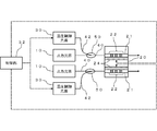
- FIG. 8 is a view showing a configuration of a light source device according to a seventh embodiment.
- This light source device is the same as any of the first to sixth embodiments except for the following points. This figure shows the same case as the sixth embodiment.
- a plurality of waveguides 21 are provided in the ferroelectric crystal 20, a plurality of waveguides 21 are provided.
- Each of the plurality of waveguides 21 has a polarization inversion structure 22.
- the output light source 10, the temperature control element 24, the temperature control light source 30, the optical fibers 40 and 42, and the multiplexing unit 50 are provided for each of the plurality of waveguides 21.
- the control unit 32 controls the plurality of temperature control elements 24 and the temperature control light source 30. In the example shown in FIG. 8, one temperature control light source 30 is provided for each of the plurality of waveguides 21, but one temperature control light source 30 may be used for each of the plurality of waveguides 21. .
- the same effect as that of the first embodiment can be obtained.
- the temperatures of the plurality of waveguides 21 can be locally controlled. Therefore, even if the plurality of waveguides 21 are formed in the same ferroelectric crystal 20, the temperature of the waveguides 21 can be individually and precisely controlled.
Landscapes
- Physics & Mathematics (AREA)
- Nonlinear Science (AREA)
- General Physics & Mathematics (AREA)
- Optics & Photonics (AREA)
- Optical Modulation, Optical Deflection, Nonlinear Optics, Optical Demodulation, Optical Logic Elements (AREA)
Abstract
強誘電体結晶(20)は、光の入力部、光の出力部、及び分極反転構造(22)を有する。分極反転構造(22)は、入力部と出力部の間に設けられている。出力光源(10)は、強誘電体結晶の入力部に出力光を入射する。出力光は、強誘電体結晶(20)の分極反転構造(22)によって波長変換される。温度制御光源(30)は、強誘電体結晶(20)の分極反転構造(22)に温度制御光を照射する。温度制御光は、強誘電体結晶(20)に吸収される波長を有している。制御部(32)は、温度制御光源(30)の出力を制御する。
Description
本発明は、分極反転構造を有する導波路を備えた光源装置及び波長変換方法に関する。
近年、擬似位相整合を用いて波長変換を行う技術が開発されている。擬似位相整合は、強誘電体結晶に分極反転構造を周期的に形成した素子を用いて行われる。
一方、擬似位相整合を用いた波長変換の効率を高くするためには、分極反転構造部分の温度を制御する必要がある。例えば特許文献1には、分極反転構造を有する導波路に薄膜ヒータを設けることが記載されている。また特許文献2には、分極反転構造を有する導波路に沿って、複数の温度制御用素子を設けることが記載されている。温度調節用素子としては、ペルチェ素子が用いられている。
ヒータやペルチェ素子は時定数が長い。このため、ヒータやペルチェ素子を用いて分極反転構造の温度制御を行った場合、分極反転構造を所望の温度にするまでに時間を要してしまう。
本発明は上記事情に鑑みてなされたものであり、その目的とするところは、分極反転構造を所望の温度にするまでの時間が短い光源装置及び波長変換方法を提供することにある。
本発明に係る光源装置は、強誘電体結晶、出力光入射部、温度制御光照射部、及び制御部を有している。強誘電体結晶は、光の入力部、光の出力部、及び分極反転構造を有する。分極反転構造は、入力部と出力部の間に設けられている。出力光入射部は、強誘電体結晶の入力部に出力光を入射する。出力光は、強誘電体結晶の分極反転構造によって波長変換される。温度制御光照射部は、強誘電体結晶の分極反転構造に温度制御光を照射する。温度制御光は、強誘電体結晶に吸収される波長を有している。制御部は、温度制御光の出力を制御する。
本発明に係る波長変換方法は、強誘電体結晶の光の入力部及び出力部の間に設けられた分極反転構造に、強誘電体結晶に吸収される波長の光である温度制御光を照射する。これにより、分極反転構造の温度が制御される。そして強誘電体結晶の入力部に、分極反転構造によって波長変換される出力光を入射することで、強誘電体結晶の出力部から、分極反転構造によって波長変換された出力光を出力させる。
本発明によれば、分極反転構造を所望の温度にするまでの時間を短くすることができる。
上述した目的、およびその他の目的、特徴および利点は、以下に述べる好適な実施の形態、およびそれに付随する以下の図面によってさらに明らかになる。
以下、本発明の実施の形態について、図面を用いて説明する。尚、すべての図面において、同様な構成要素には同様の符号を付し、適宜説明を省略する。
(第1の実施形態)
図1は、第1の実施形態に係る光源装置の構成を示す図である。この光源装置は、強誘電体結晶20、出力光源10、温度制御光源30、及び制御部32を備えている。
図1は、第1の実施形態に係る光源装置の構成を示す図である。この光源装置は、強誘電体結晶20、出力光源10、温度制御光源30、及び制御部32を備えている。
強誘電体結晶20は、例えばMgを添加したLiNbO3であるが、これに限定されない。強誘電体結晶20は、光の入力部及び出力部を有している。本図に示す例では、強誘電体結晶20には導波路21が形成されている。導波路21の構造は限定されない。導波路21は、例えばリッジ構造であっても良いし、埋め込み形であってもよい。そして導波路21の一端が光の入力部になっており、他端が光の出力部になっている。分極反転構造22は、導波路21に設けられている。分極反転構造22の分極反転の周期は、出力光源10が出力する光の波長に基づいて定められている。
出力光源10は、光ファイバ40を介して導波路21の入力側端部に結合している。出力光源10は、導波路21に、出力光を入射する。この出力光は、導波路21の分極反転構造22によって波長変換される波長を有している。すなわち出力光源10の出力光は、導波路21の分極反転構造22で波長変換された後、導波路21の出力側端部から出射される。
温度制御光源30は、導波路21の分極反転構造22に、温度制御光を照射する。温度制御光は、強誘電体結晶20に吸収される波長を有する。温度制御光は、強誘電体結晶20における吸収率が10%以上90%以下の範囲であるのが好ましい。温度制御光の波長は、例えば強誘電体結晶20の短波長側の吸収領域の吸収端よりも短いか、又は、強誘電体結晶20の長波長側の吸収領域の吸収端よりも長い。例えば強誘電体結晶20がMgを添加したLiNbO3である場合、温度制御光の波長は、例えば300nm以下、又は4.5μm以上である。
本図に示す例では、温度制御光源30は、導波路21の入力側端部に温度制御光を入射している。具体的には、温度制御光源30は、光ファイバ42に温度制御光を出力する。光ファイバ42は、合波部50(例えばカプラ)を介して光ファイバ40に繋がっている。このため光ファイバ42に入射した温度制御光は、合波部50及び光ファイバ40を介して、導波路21の入力側端部に入力される。
なお、強誘電体結晶20に導波路を形成せず、強誘電体結晶20をバルクのまま使用しても良い。また温度制御光源30は、発光する光の波長が固定されていても良いし、可変であっても良い。また本図に示す例では、温度制御光源30を一つのみ設けている。ただし、互いに異なる波長の光を発光する複数の温度制御光源30を設けても良い。
また、出力光源10と強誘電体結晶20の間の光路は光ファイバ40ではなく、レンズやミラーによって形成されていても良い。同様に、温度制御光源30と強誘電体結晶20の間の光路は光ファイバ42ではなく、レンズやミラーによって形成されていても良い。
制御部32は、温度制御光源30の出力を制御する。
次に、本実施形態の作用及び効果について説明する。本実施形態において、温度制御光源30は、分極反転構造22に温度制御光を照射する。温度制御光は、強誘電体結晶20に吸収される波長を有している。このため、温度制御光源30の出力を制御することにより、分極反転構造22の温度を制御することができる。温度制御光源30の出力の制御性は高い。従って、ヒータやペルチェ素子のみで温度調節を行う場合と比較して、分極反転構造22が所望の温度になるまでの時間は短くなる。
また本実施形態では、温度調節光を導波路21の入力側端部から入射している。従って、分極反転構造22を局所的に加熱することができる。従って、分極反転構造22が所望の温度になるまでの時間は、さらに短くなる。
(第2の実施形態)
図2は、第2の実施形態に係る光源装置の構成を示す図である。この光源装置は、光ファイバ42が直接強誘電体結晶20に接続している点を除いて、第1の実施形態に係る光源装置と同様の構成である。
本実施形態によっても、第1の実施形態と同様の効果を得ることができる。
図2は、第2の実施形態に係る光源装置の構成を示す図である。この光源装置は、光ファイバ42が直接強誘電体結晶20に接続している点を除いて、第1の実施形態に係る光源装置と同様の構成である。
本実施形態によっても、第1の実施形態と同様の効果を得ることができる。
(第3の実施形態)
図3は、第3の実施形態に係る光源装置の構成を示す図である。この光源装置は、温度制御光源30が温度制御光を分極反転構造22の側部に照射する点を除いて、第1の実施形態に係る光源装置と同様の構成である。
本実施形態によっても、第1の実施形態と同様の効果を得ることができる。
図3は、第3の実施形態に係る光源装置の構成を示す図である。この光源装置は、温度制御光源30が温度制御光を分極反転構造22の側部に照射する点を除いて、第1の実施形態に係る光源装置と同様の構成である。
本実施形態によっても、第1の実施形態と同様の効果を得ることができる。
(第4の実施形態)
図4は、第4の実施形態に係る光源装置の構成を示す図である。この光源装置は、出力検出部34を有している点を除いて、第1~第3の実施形態のいずれかに示した光源装置と同様の構成である。本図は、第1の実施形態と同様の場合を示している。
図4は、第4の実施形態に係る光源装置の構成を示す図である。この光源装置は、出力検出部34を有している点を除いて、第1~第3の実施形態のいずれかに示した光源装置と同様の構成である。本図は、第1の実施形態と同様の場合を示している。
出力検出部34は、導波路21の出力側端部から出力される出力光の強度を検出する。出力検出部34による検出結果は、制御部32に送信される。制御部32は、出力検出部34から受信した検出結果に基づいて、温度制御光源30の出力を制御する。具体的には、制御部32は、出力検出部34が検出した強度が最大となるように、温度制御光源30の出力を制御する。
なお図5に示すように、分岐部52を用いることで強誘電体結晶20から出力された出力光の一部を分岐し、出力検出部34に入射するようにしてもよい。このようにすると、出力検出部34が強誘電体結晶20の出力に与える影響を少なくすることができる。
本実施形態によっても、第1の実施形態と同様の効果を得ることができる。また、制御部32は、出力検出部34から受信した検出結果に基づいて、温度制御光源30の出力を制御する。従って、分極反転構造22の温度制御を容易に行うことができる。
(第5の実施形態)
図6は、第5の実施形態に係る光源装置の構成を示す図である。この光源装置は、温度検出部36を有している点を除いて、第1~第3の実施形態のいずれかに示した光源装置と同様の構成である。本図は、第1の実施形態と同様の場合を示している。
図6は、第5の実施形態に係る光源装置の構成を示す図である。この光源装置は、温度検出部36を有している点を除いて、第1~第3の実施形態のいずれかに示した光源装置と同様の構成である。本図は、第1の実施形態と同様の場合を示している。
温度検出部36は、分極反転構造22の温度を検出する。温度検出部36による検出結果は、制御部32に送信される。制御部32は、温度検出部36から受信した検出結果に基づいて、温度制御光源30の出力を制御する。具体的には、制御部32は、温度検出部36が検出した温度が予め定められた値となるように、温度制御光源30の出力を制御する。
本実施形態によっても、第1の実施形態と同様の効果を得ることができる。また、制御部32は、温度検出部36から受信した検出結果に基づいて、温度制御光源30の出力を制御する。従って、分極反転構造22の温度制御を容易に行うことができる。
(第6の実施形態)
図7は、第6の実施形態に係る光源装置の構成を示す図である。この光源装置は、温度調節素子24を有している点を除いて、第1~第5の実施形態のいずれかに示した光源装置と同様の構成である。本図は、第1の実施形態と同様の場合を示している。
図7は、第6の実施形態に係る光源装置の構成を示す図である。この光源装置は、温度調節素子24を有している点を除いて、第1~第5の実施形態のいずれかに示した光源装置と同様の構成である。本図は、第1の実施形態と同様の場合を示している。
温度調節素子24は、強誘電体結晶20のうち導波路21の近傍に取り付けられており、発熱及び吸熱の少なくとも一方を行う。温度調節素子24は、例えばヒータ又はペルチェ素子である。温度調節素子24は、制御部32によって制御される。
制御部32は、温度調節素子24をメインの温度調節機構として使用し、温度制御光源30をサブの温度調節機構として用いる。具体的には、温度調節素子24を用いてある程度分極反転構造22の温度を制御しておき、温度制御光源30を用いて分極反転構造22の温度の微調整を行う。このため、温度調節素子24の稼働時間は、温度制御光源30の稼働時間よりも長くなる。
本実施形態によっても、第1の実施形態と同様の効果を得ることができる。また温度調節素子24をメインの温度調節機構として使用しているため、分極反転構造22の温度制御範囲が広くなる。
(第7の実施形態)
図8は、第7の実施形態に係る光源装置の構成を示す図である。この光源装置は、以下の点を除いて第1~第6の実施形態のいずれかと同様である。本図は、第6の実施形態と同様の場合を示している。
図8は、第7の実施形態に係る光源装置の構成を示す図である。この光源装置は、以下の点を除いて第1~第6の実施形態のいずれかと同様である。本図は、第6の実施形態と同様の場合を示している。
まず、強誘電体結晶20には、複数の導波路21が設けられている。複数の導波路21は、いずれも分極反転構造22を有している。
そして出力光源10、温度調節素子24、温度制御光源30、光ファイバ40,42、及び合波部50は、複数の導波路21それぞれに対して設けられている。制御部32は、複数の温度調節素子24及び温度制御光源30を制御している。なお、図8に示す例では、複数の導波路21に対して温度制御光源30を一つずつ設けているが、複数の導波路21に対して、一つの温度制御光源30を用いてもよい。
本実施形態によっても、第1の実施形態と同様の効果を得ることができる。また、温度制御光源30を制御することにより、複数の導波路21の温度を局所的に制御することができる。従って、複数の導波路21が同一の強誘電体結晶20に形成されていても、導波路21の温度を個別に精度よく制御することができる。
以上、図面を参照して本発明の実施形態について述べたが、これらは本発明の例示であり、上記以外の様々な構成を採用することもできる。
この出願は、2011年11月14日に出願された日本出願特願2011-248395を基礎とする優先権を主張し、その開示の全てをここに取り込む。
Claims (8)
- 光の入力部、前記光の出力部、及び前記入力部と前記出力部の間に設けられた分極反転構造を有する強誘電体結晶と、
前記入力部に、前記分極反転構造によって波長変換される出力光を入射する出力光入射部と、
前記分極反転構造に、前記強誘電体結晶に吸収される波長の光である温度制御光を照射する温度制御光照射部と、
前記温度制御光の出力を制御する制御部と、
を備える光源装置。 - 請求項1に記載の光源装置において、
前記温度制御光照射部は、前記入力部に前記温度制御光を入射する光源装置。 - 請求項1又は2に記載の光源装置において、
前記分極反転構造に設けられ、発熱及び吸熱の少なくとも一方を行う温度調節素子を備える光源装置。 - 請求項3に記載の光源装置において、
前記制御部は、前記温度調節素子の出力を制御し、
前記温度調節素子の稼働時間は、前記温度制御光照射部の稼働時間よりも長い光源装置。 - 請求項1~4のいずれか一項に記載の光源装置において、
前記出力部から出力される前記出力光の強度を検出する出力検出部を備え、
前記制御部は、前記出力検出部の検出結果に基づいて、前記温度制御光の強度を制御する光源装置。 - 請求項1~4のいずれか一項に記載の光源装置において、
前記分極反転構造の温度を検出する温度検出部を備え、
前記制御部は、前記温度検出部の検出結果に基づいて、前記温度制御光の強度を制御する光源装置。 - 請求項1~6のいずれか一項に記載の光源装置において、
前記強誘電体結晶は、複数の導波路を備え、
前記複数の導波路は、それぞれ前記入力部及び前記出力部を有しており、
前記出力光入射部及び前記温度制御光照射部は、前記複数の導波路それぞれに対して設けられている光源装置。 - 強誘電体結晶の光の入力部及び出力部の間に設けられた分極反転構造に、前記強誘電体結晶に吸収される波長の光である温度制御光を照射することで前記分極反転構造の温度を制御し、
前記入力部に、前記分極反転構造によって波長変換される出力光を入射することで、前記出力部から、前記分極反転構造によって波長変換された前記出力光を出力させる、波長変換方法。
Applications Claiming Priority (2)
| Application Number | Priority Date | Filing Date | Title |
|---|---|---|---|
| JP2011248395A JP2015025825A (ja) | 2011-11-14 | 2011-11-14 | 光源装置及び波長変換方法 |
| JP2011-248395 | 2011-11-14 |
Publications (1)
| Publication Number | Publication Date |
|---|---|
| WO2013073080A1 true WO2013073080A1 (ja) | 2013-05-23 |
Family
ID=48429185
Family Applications (1)
| Application Number | Title | Priority Date | Filing Date |
|---|---|---|---|
| PCT/JP2012/005205 Ceased WO2013073080A1 (ja) | 2011-11-14 | 2012-08-20 | 光源装置及び波長変換方法 |
Country Status (3)
| Country | Link |
|---|---|
| JP (1) | JP2015025825A (ja) |
| TW (1) | TW201326935A (ja) |
| WO (1) | WO2013073080A1 (ja) |
Families Citing this family (1)
| Publication number | Priority date | Publication date | Assignee | Title |
|---|---|---|---|---|
| WO2022157858A1 (ja) * | 2021-01-20 | 2022-07-28 | 日本電信電話株式会社 | 波長変換装置 |
Citations (6)
| Publication number | Priority date | Publication date | Assignee | Title |
|---|---|---|---|---|
| JPH04109226A (ja) * | 1990-08-30 | 1992-04-10 | Hitachi Metals Ltd | 波長変換素子 |
| JPH0876160A (ja) * | 1994-09-06 | 1996-03-22 | Oki Electric Ind Co Ltd | 波長変換装置およびその製造方法 |
| WO2008050802A1 (en) * | 2006-10-27 | 2008-05-02 | Panasonic Corporation | Short wavelength light source and laser image forming device |
| WO2008093545A1 (ja) * | 2007-01-29 | 2008-08-07 | Panasonic Corporation | 固体レーザー装置、表示装置及び波長変換素子 |
| JP2009122252A (ja) * | 2007-11-13 | 2009-06-04 | Seiko Epson Corp | 複数波長光源装置 |
| JP2010217250A (ja) * | 2009-03-13 | 2010-09-30 | Seiko Epson Corp | 波長変換装置、光源装置及びプロジェクター |
-
2011
- 2011-11-14 JP JP2011248395A patent/JP2015025825A/ja active Pending
-
2012
- 2012-08-20 WO PCT/JP2012/005205 patent/WO2013073080A1/ja not_active Ceased
- 2012-11-12 TW TW101142029A patent/TW201326935A/zh unknown
Patent Citations (6)
| Publication number | Priority date | Publication date | Assignee | Title |
|---|---|---|---|---|
| JPH04109226A (ja) * | 1990-08-30 | 1992-04-10 | Hitachi Metals Ltd | 波長変換素子 |
| JPH0876160A (ja) * | 1994-09-06 | 1996-03-22 | Oki Electric Ind Co Ltd | 波長変換装置およびその製造方法 |
| WO2008050802A1 (en) * | 2006-10-27 | 2008-05-02 | Panasonic Corporation | Short wavelength light source and laser image forming device |
| WO2008093545A1 (ja) * | 2007-01-29 | 2008-08-07 | Panasonic Corporation | 固体レーザー装置、表示装置及び波長変換素子 |
| JP2009122252A (ja) * | 2007-11-13 | 2009-06-04 | Seiko Epson Corp | 複数波長光源装置 |
| JP2010217250A (ja) * | 2009-03-13 | 2010-09-30 | Seiko Epson Corp | 波長変換装置、光源装置及びプロジェクター |
Also Published As
| Publication number | Publication date |
|---|---|
| JP2015025825A (ja) | 2015-02-05 |
| TW201326935A (zh) | 2013-07-01 |
Similar Documents
| Publication | Publication Date | Title |
|---|---|---|
| KR102090454B1 (ko) | 레이저 장치, 그 레이저 장치를 구비한 노광 장치 및 검사 장치 | |
| WO2012033105A1 (ja) | レーザ装置 | |
| TWI567471B (zh) | A light source device, an analyzing device, and a light generating method | |
| JP6016086B2 (ja) | 紫外レーザ装置、この紫外レーザ装置を備えた露光装置及び検査装置 | |
| JP6016124B2 (ja) | パルスレーザ装置、露光装置および検査装置 | |
| WO2013073080A1 (ja) | 光源装置及び波長変換方法 | |
| WO2013069179A1 (ja) | 光源装置及び波長変換方法 | |
| JP2013156448A (ja) | レーザ装置、露光装置及び検査装置 | |
| CN103348286A (zh) | 紫外线激光装置 | |
| JP2011158869A (ja) | 波長変換装置 | |
| JP2015087729A (ja) | 波長変換レーザ装置 | |
| JP2015180903A (ja) | レーザ装置、該レーザ装置を備えた露光装置及び検査装置 | |
| JP2015187636A (ja) | 光モジュール | |
| US7974320B2 (en) | Method for having laser light source in standby status | |
| JP5305823B2 (ja) | 温調装置 | |
| JP5566966B2 (ja) | 半導体光素子 | |
| JP2013007931A (ja) | レーザ装置、露光装置及び検査装置 | |
| JP5780457B2 (ja) | レーザ装置、レーザ装置を備えた露光装置及び検査装置 | |
| WO2023037560A1 (ja) | 波長変換器およびその制御方法 | |
| US9166359B2 (en) | Method and laser oscillator for the generation of a laser beam | |
| JP2013044764A (ja) | レーザ装置、疑似位相整合型の波長変換光学素子のフォトリフラクティブ効果抑制方法、露光装置及び検査装置 | |
| JP5464972B2 (ja) | レーザ加工装置 | |
| JP2014033044A (ja) | ダブルクラッドファイバ、このダブルクラッドファイバを備えたレーザ装置、露光装置及び検査装置 | |
| KR20100086835A (ko) | 레이저 광분할 제어시스템 | |
| JP2012175102A (ja) | 投影露光装置へ電磁放射を案内する装置 |
Legal Events
| Date | Code | Title | Description |
|---|---|---|---|
| 121 | Ep: the epo has been informed by wipo that ep was designated in this application |
Ref document number: 12849168 Country of ref document: EP Kind code of ref document: A1 |
|
| NENP | Non-entry into the national phase |
Ref country code: DE |
|
| 122 | Ep: pct application non-entry in european phase |
Ref document number: 12849168 Country of ref document: EP Kind code of ref document: A1 |
|
| NENP | Non-entry into the national phase |
Ref country code: JP |