WO2013065146A1 - 発光装置 - Google Patents
発光装置 Download PDFInfo
- Publication number
- WO2013065146A1 WO2013065146A1 PCT/JP2011/075308 JP2011075308W WO2013065146A1 WO 2013065146 A1 WO2013065146 A1 WO 2013065146A1 JP 2011075308 W JP2011075308 W JP 2011075308W WO 2013065146 A1 WO2013065146 A1 WO 2013065146A1
- Authority
- WO
- WIPO (PCT)
- Prior art keywords
- optical member
- light emitting
- emitting device
- wall
- mounting substrate
- Prior art date
Links
Images


Classifications
-
- F—MECHANICAL ENGINEERING; LIGHTING; HEATING; WEAPONS; BLASTING
- F21—LIGHTING
- F21V—FUNCTIONAL FEATURES OR DETAILS OF LIGHTING DEVICES OR SYSTEMS THEREOF; STRUCTURAL COMBINATIONS OF LIGHTING DEVICES WITH OTHER ARTICLES, NOT OTHERWISE PROVIDED FOR
- F21V5/00—Refractors for light sources
- F21V5/007—Array of lenses or refractors for a cluster of light sources, e.g. for arrangement of multiple light sources in one plane
-
- F—MECHANICAL ENGINEERING; LIGHTING; HEATING; WEAPONS; BLASTING
- F21—LIGHTING
- F21S—NON-PORTABLE LIGHTING DEVICES; SYSTEMS THEREOF; VEHICLE LIGHTING DEVICES SPECIALLY ADAPTED FOR VEHICLE EXTERIORS
- F21S4/00—Lighting devices or systems using a string or strip of light sources
- F21S4/20—Lighting devices or systems using a string or strip of light sources with light sources held by or within elongate supports
- F21S4/28—Lighting devices or systems using a string or strip of light sources with light sources held by or within elongate supports rigid, e.g. LED bars
-
- F—MECHANICAL ENGINEERING; LIGHTING; HEATING; WEAPONS; BLASTING
- F21—LIGHTING
- F21V—FUNCTIONAL FEATURES OR DETAILS OF LIGHTING DEVICES OR SYSTEMS THEREOF; STRUCTURAL COMBINATIONS OF LIGHTING DEVICES WITH OTHER ARTICLES, NOT OTHERWISE PROVIDED FOR
- F21V17/00—Fastening of component parts of lighting devices, e.g. shades, globes, refractors, reflectors, filters, screens, grids or protective cages
- F21V17/005—Fastening of component parts of lighting devices, e.g. shades, globes, refractors, reflectors, filters, screens, grids or protective cages with keying means, i.e. for enabling the assembling of component parts in distinctive positions, e.g. for preventing wrong mounting
-
- F—MECHANICAL ENGINEERING; LIGHTING; HEATING; WEAPONS; BLASTING
- F21—LIGHTING
- F21V—FUNCTIONAL FEATURES OR DETAILS OF LIGHTING DEVICES OR SYSTEMS THEREOF; STRUCTURAL COMBINATIONS OF LIGHTING DEVICES WITH OTHER ARTICLES, NOT OTHERWISE PROVIDED FOR
- F21V19/00—Fastening of light sources or lamp holders
- F21V19/001—Fastening of light sources or lamp holders the light sources being semiconductors devices, e.g. LEDs
- F21V19/003—Fastening of light source holders, e.g. of circuit boards or substrates holding light sources
- F21V19/0035—Fastening of light source holders, e.g. of circuit boards or substrates holding light sources the fastening means being capable of simultaneously attaching of an other part, e.g. a housing portion or an optical component
-
- F—MECHANICAL ENGINEERING; LIGHTING; HEATING; WEAPONS; BLASTING
- F21—LIGHTING
- F21V—FUNCTIONAL FEATURES OR DETAILS OF LIGHTING DEVICES OR SYSTEMS THEREOF; STRUCTURAL COMBINATIONS OF LIGHTING DEVICES WITH OTHER ARTICLES, NOT OTHERWISE PROVIDED FOR
- F21V19/00—Fastening of light sources or lamp holders
- F21V19/001—Fastening of light sources or lamp holders the light sources being semiconductors devices, e.g. LEDs
- F21V19/003—Fastening of light source holders, e.g. of circuit boards or substrates holding light sources
- F21V19/0055—Fastening of light source holders, e.g. of circuit boards or substrates holding light sources by screwing
-
- F—MECHANICAL ENGINEERING; LIGHTING; HEATING; WEAPONS; BLASTING
- F21—LIGHTING
- F21V—FUNCTIONAL FEATURES OR DETAILS OF LIGHTING DEVICES OR SYSTEMS THEREOF; STRUCTURAL COMBINATIONS OF LIGHTING DEVICES WITH OTHER ARTICLES, NOT OTHERWISE PROVIDED FOR
- F21V23/00—Arrangement of electric circuit elements in or on lighting devices
- F21V23/06—Arrangement of electric circuit elements in or on lighting devices the elements being coupling devices, e.g. connectors
-
- F—MECHANICAL ENGINEERING; LIGHTING; HEATING; WEAPONS; BLASTING
- F21—LIGHTING
- F21Y—INDEXING SCHEME ASSOCIATED WITH SUBCLASSES F21K, F21L, F21S and F21V, RELATING TO THE FORM OR THE KIND OF THE LIGHT SOURCES OR OF THE COLOUR OF THE LIGHT EMITTED
- F21Y2103/00—Elongate light sources, e.g. fluorescent tubes
- F21Y2103/10—Elongate light sources, e.g. fluorescent tubes comprising a linear array of point-like light-generating elements
-
- F—MECHANICAL ENGINEERING; LIGHTING; HEATING; WEAPONS; BLASTING
- F21—LIGHTING
- F21Y—INDEXING SCHEME ASSOCIATED WITH SUBCLASSES F21K, F21L, F21S and F21V, RELATING TO THE FORM OR THE KIND OF THE LIGHT SOURCES OR OF THE COLOUR OF THE LIGHT EMITTED
- F21Y2115/00—Light-generating elements of semiconductor light sources
- F21Y2115/10—Light-emitting diodes [LED]
Definitions
- the present invention relates to a light emitting device.
- an LED illumination device As a light-emitting device, in the following Patent Document 1, an LED illumination device is proposed.
- This LED illumination device includes a box-shaped housing that opens upward and a lid that closes the opening of the housing.
- a substrate on which a plurality of LEDs are mounted is housed inside the housing, and a lens unit for collecting and distributing light emitted from the LEDs is provided on the substrate.
- the lens unit includes a bottom plate portion on which a lens is provided, and a pair of side plate portions disposed in the vertical direction perpendicular to the bottom plate portion on both sides of the bottom plate portion.
- a long hole extending in the lateral direction is formed in a penetrating manner at an upper position in each of the side plate portions.
- a protruding portion that protrudes upward is formed on the top surface, and a leg portion that protrudes downward is formed on the bottom surface.
- the leg portion In the lens unit housed in the housing, the leg portion is inserted into an attachment hole provided in the substrate, and the protruding portion is pressed from above by the lid. Thereby, in each side plate part of a lens unit, the part around a long hole is compressed up and down, and is elastically deformed. That is, the lens unit is elastically held in the housing.
- the light-emitting device can be used in various environments, it is necessary to assume the use in an environment that is susceptible to vibration and impact.
- the lens unit since the lens unit is elastically held in the housing, it is not fixed at a fixed position. Therefore, when vibration or impact is applied to the LED lighting device, the lens in the housing is The unit position may change. As the position of the lens unit changes, the relative position between the lens unit and the LED shifts. Therefore, the light condensing characteristics and light distribution characteristics (from the LEDs) in the lens unit (hereinafter collectively referred to as “optical characteristics”). May cause a problem that changes.
- an object of the present invention is to provide a light emitting device capable of improving vibration resistance and impact resistance.
- the invention according to claim 1 includes a housing (2) having an opening (18) and an internal space (19), and a light emitting element (16) disposed in the internal space.
- a light emitting device (3) including a mounted substrate (3) mounted, an optical member (4) disposed forward on the optical axis (X) of the light emitting element, and a transparent cover (5) attached to the opening. 1), a fixing wall (20) for partitioning a part of the internal space and fixing the mounting board in a fixed position, and a light emission provided and mounted on the mounting board.
- the optical member is attached to the mounting substrate by fitting the positioning convex portion of the optical member to the positioning concave portion of the mounting substrate fixed in place by the fixing wall of the housing. It is positioned and fixed with respect to it. Further, the pressing member of the transparent cover presses the optical member so that the fitting between the positioning concave portion and the convex portion does not shift, so that the optical member is fixed to the transparent cover and the mounting substrate (in other words, the mounting substrate is fixed). Between the housing and the housing.
- the relative position between the optical member and the mounting substrate is firmly fixed, even if vibration or impact is applied to the light emitting device, the relative position does not change, and the optical member (from the light emitting element) is not changed. )
- the optical characteristics of light can be kept constant.
- the optical member is not elastically held in the housing, even if vibration or impact is applied to the light emitting device, fatigue is less likely to accumulate in the optical member. Therefore, the optical member is caused by vibration or impact. There is no damage.
- the casing rises from a side edge (20B, 20C) of the fixing wall, defines a part of the internal space, and supports a side portion of the optical member.
- (21) It is a light-emitting device of Claim 1. According to this configuration, since the side of the optical member is supported by the side wall of the housing, the position of the optical member is further stabilized. Therefore, even if vibration or impact is applied to the light emitting device, the optical member and the mounting substrate It is possible to further suppress the change in the relative position. Therefore, the vibration resistance and impact resistance of the light emitting device can be further improved.
- the side edges of the fixing wall include at least a pair of side edges opposed to each other, and a pair of the side walls are provided so as to rise from each of the pair of side edges.
- the side portions on both sides of the optical member are supported by the pair of side walls, so that the position of the optical member is further stabilized. Therefore, even if vibration or impact is applied to the light emitting device, it is possible to further suppress the change in the relative position between the optical member and the mounting substrate. Therefore, the vibration resistance and impact resistance of the light emitting device can be further improved.
- the casing rises from the outer edge (22D) of the shelf wall and faces each other across the opening, and supports a pair of side surfaces (5C, 5D) of the transparent cover.
- the optical member has an engaging convex portion (13) projecting outward, and the pair of side walls have an engaging concave portion (28) for receiving the engaging convex portion.
- the optical member and the mounting board are positioned with respect to a common object called a housing, it is possible to further suppress the change in the relative position between the optical member and the mounting board. Therefore, the vibration resistance and impact resistance of the light emitting device can be further improved.
- the engaging concave portion is open to the shelf wall side, and an upper end of the engaging convex portion received in the engaging concave portion is substantially flush with the shelf wall.
- the light-emitting device according to claim 6. according to this configuration, in a state where the side portion of the transparent cover is received by the shelf wall of the housing, the side portion of the transparent cover (corresponding to the pressing portion) is the engagement convex portion (strictly speaking, in the optical member). Only the upper end portion exposed to the shelf wall side from the engaging recess is pressed down.
- the transparent cover presses only a part of the outer peripheral side (engagement convex portion) of the optical member, so that no extra stress (distortion or the like) is generated on the entire optical member. Therefore, it is possible to suppress a change in the relative position between the optical member and the mounting substrate due to the transparent cover, so that the optical characteristics of light (from the light emitting element) in the optical member can be maintained constant.
- the invention according to claim 8 is characterized in that the optical member has a support column (9) depending from a peripheral portion thereof, and the positioning convex portion is provided at a lower end of the support column.
- Item 8 The light emitting device according to any one of Items 1 to 7. According to this configuration, the positioning convex portion can be provided on the optical member with a simple configuration in which the support is provided on the optical member.
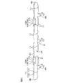
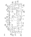
- FIG. 1 is a perspective view of a light emitting device 1 according to an embodiment of the present invention as viewed from above.
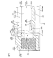
- FIG. 2 is an exploded perspective view of the light emitting device 1 as viewed from above.
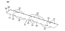
- FIG. 3A is a perspective view of one optical member 4 in the light emitting device 1 as viewed from below.
- FIG. 3B is a side view of the optical member 4 viewed from a predetermined direction.
- 3C is a side view of the optical member 4 viewed from a direction different from that in FIG. 3B.
- FIG. 4 is a perspective view of the mounting substrate 3 in the light emitting device 1 as viewed from below.
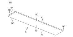
- FIG. 5 is a perspective view of the transparent cover 5 in the light emitting device 1 as viewed from below.
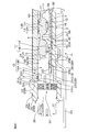
- FIG. 6 is a plan view of the housing 2 in the light emitting device 1.
- FIG. 7A is an AA arrow view of FIG.
- FIG. 7B is a BB arrow view of FIG.
- FIG. 7C is a CC arrow view of FIG.
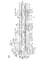
- FIG. 8 is a plan view of the light emitting device 1 in a completed state.
- FIG. 9A is an AA arrow view of FIG.
- FIG. 9B is a BB arrow view of FIG.
- FIG. 9C is a CC arrow view of FIG.
- FIG. 9D is a DD arrow view of FIG.
- FIG. 9E is an EE arrow view of FIG.
- FIG. 1 is a perspective view of a light emitting device 1 according to an embodiment of the present invention as viewed from above.
- the light-emitting device 1 which concerns on one Embodiment of this invention has comprised the rectangular parallelepiped shape elongated in the predetermined direction.
- the horizontal direction, the width direction, and the vertical direction of the light emitting device 1 will be used.
- the lateral direction is the longitudinal direction of the light emitting device 1, and is the direction connecting the upper left and the lower right in FIG.
- the width direction is the short direction perpendicular to the longitudinal direction in the light emitting device 1, In FIG. 1, it is the direction connecting the lower left and the upper right.
- the vertical direction is a direction orthogonal to both the long direction and the short direction.
- FIG. 2 is an exploded perspective view of the light emitting device 1 as viewed from above.
- the light emitting device 1 includes a housing 2, a mounting substrate 3 serving as a light source, and a plurality (here, three) optical members 4 that collect and distribute light from the mounting substrate 3. And a transparent cover 5, a plurality (here, six) fixing screws 6, a connector block 7, and a plurality (here, two) fixing bolts 8 are mainly included.
- FIG. 3A is a perspective view of one optical member 4 in the light emitting device 1 as viewed from below.
- FIG. 3B is a side view of the optical member 4 viewed from a predetermined direction.
- 3C is a side view of the optical member 4 viewed from a direction different from that in FIG. 3B.
- FIG. 3A to FIG. 3C are referred to as needed in addition to FIG.
- the optical member 4 is formed of a transparent (including translucent) resin.
- the optical member 4 has a thin plate shape in the vertical direction. Since the optical member 4 in plan view has a long rectangular shape in the horizontal direction, it has a pair of long sides 4A extending in parallel along the horizontal direction and a pair of short sides 4B extending in the width direction. ing.
- both end portions in the width direction are bent downward at substantially right angles over the entire lateral direction, and the width direction outer end surfaces of the portions bent at the both end portions are the aforementioned.
- the long side 4A is defined.
- both end portions in the width direction have portions that hang downward.
- a plurality (three in this case) of columns 9 are provided at equal positions in the lateral direction at positions extending along the inner side in the width direction at the respective hanging portions of the both end portions. Therefore, six struts 9 are provided for one optical member 4.
- the support column 9 has a cylindrical shape extending vertically and is integrated with the optical member 4.
- the three support pillars 9 located on the same side in the width direction are suspended from a position (peripheral edge of the optical member 4) along the width direction inner side with respect to the long side 4A on the same side in the width direction.
- a positioning convex portion 10 that protrudes downward from the circular center position of the column 9 is integrally provided on the lower end surface 9 ⁇ / b> A of each column 9, a positioning convex portion 10 that protrudes downward from the circular center position of the column 9 is integrally provided.
- the positioning convex portion 10 has a columnar shape that is thinner than the column 9.
- the lower end of the positioning convex portion 10 is the lower end of the entire optical member 4 (see FIG. 3B).
- the positioning convex portion 10 can be provided on the optical member 4 with a simple configuration in which only the support column 9 is provided.
- each lens 11 bulges downward from the bottom surface 4 ⁇ / b> C of the optical member 4 in a circular arc shape and from the top surface 4 ⁇ / b> D of the optical member 4 to an upward arc shape. And an upper bulging portion 11B.
- the lower bulge portion 11A has a larger bulge amount (thickness in the vertical direction) than the upper bulge portion 11B.
- the lower end surface of the lower bulging portion 11 ⁇ / b> A is located above the lower end surface 9 ⁇ / b> A of each column 9.
- the lower end surface of the lower bulging portion 11A is flat along the lateral direction and the width direction (sometimes collectively referred to as the “horizontal direction”), and the lower end surface has a depression 12 that is slightly recessed upward. Is formed.
- the width direction end portions (portions bent downward), the columns 9 and the portions other than the lower bulging portion 11A of the lens 11 are substantially flat along the horizontal direction.
- two engaging convex portions 13 are provided at positions along each of the pair of long sides 4 ⁇ / b> A on the top surface 4 ⁇ / b> D of the optical member 4. That is, one optical member 4 has four engagement convex portions 13. In each long side 4A, the two engaging convex parts 13 are spaced apart in the lateral direction.
- One engaging convex portion 13 is arranged (see FIGS. 3A and 3C).
- Each engagement convex part 13 has protruded to the outer side (width direction outer side) rather than 4 A of long sides. Strictly, with reference to FIG. 3B, each engaging convex part 13 once extends upward from the long side 4A (end part in the width direction of the optical member 4) and then extends outward in the width direction. In a plan view, each engagement convex portion 13 has a substantially isosceles trapezoidal shape that becomes narrower toward the outside in the width direction (see FIGS. 2 and 3A). In each engaging convex portion 13, an upper convex portion 13A that rises upward is integrally provided in front (inner side) of the width direction outer end. The upper end surface 13B of the upper convex portion 13A is flat along the horizontal direction.
- the upper end surface 13B is the upper end of the engaging convex portion 13, and is also the upper end of the entire optical member 4. Therefore, the upper end surface of the upper bulging portion 11B of each lens 11 is positioned below the upper end surface 13B of the upper convex portion 13A.
- FIG. 4 is a perspective view of the mounting substrate 3 in the light emitting device 1 as viewed from below.
- the mounting substrate 3 has a thin plate shape in the vertical direction, and has a rectangular shape that is long in the horizontal direction in plan view. In the horizontal direction, the mounting substrate 3 has substantially the same length as the group of three optical members 4 connected in the horizontal direction (see FIG. 2).
- One of the four corners of the mounting substrate 3 in plan view is a cutout portion 3 ⁇ / b> A cut obliquely.
- the top surface 3B (see FIG. 2) and the bottom surface 3C (see FIG. 4) of the mounting substrate 3 are both flat along the horizontal direction.
- each positioning recess 14 is provided in the top surface 3 ⁇ / b> B of the mounting substrate 3.
- the positioning recess 14 is for positioning the optical member 4 on the mounting substrate 3.
- Nine positioning recesses 14 are arranged at equal intervals in the lateral direction at each of the widthwise ends of the top surface 3B.
- Each positioning recess 14 is recessed downward from the top surface 3B.
- the positioning recess 14 penetrates the mounting substrate 3 in the vertical direction (thickness direction) (see FIG. 4), but does not have to penetrate the mounting substrate 3.
- each positioning recess 14 has a circular shape slightly larger in diameter than the positioning protrusion 10 (see FIG. 3A) described above.
- each of the widthwise end portions of the top surface 3B of the mounting substrate 3 a plurality (three in this case) of screws are inserted into the region between the positioning recesses 14 at both ends in the positioning recesses 14 arranged in the lateral direction.
- the holes 15 are formed at predetermined intervals (not necessarily equal intervals) in the lateral direction.
- a total of six screw insertion holes 15 are formed in the mounting substrate 3.
- Each screw insertion hole 15 is a round hole penetrating the mounting substrate 3 in the vertical direction, and is formed so as to avoid the positioning recess 14.
- One fixing screw 6 is inserted into each screw insertion hole 15 from the top surface 3B side (above) (described later).
- a plurality of (in this case, 18) light emitting elements 16 are disposed in the entire region in the lateral direction in the region sandwiched between the positioning recesses 14 and the screw insertion holes 15 on both sides in the width direction. It is mounted at equal intervals.
- the light emitting element 16 in this embodiment is an LED (light emitting diode). Light is emitted from the upper surface of the light emitting element 16. Note that a large number of small holes (not shown) for releasing the heat of the light emitting elements 16 may be formed around the light emitting elements 16 in the mounting substrate 3.
- FIG. 5 is a perspective view of the transparent cover 5 in the light emitting device 1 as viewed from below.
- FIG. 5 is also referred to together with FIG.
- the transparent cover 5 has a thin plate shape in the top and bottom formed of transparent (including translucent) resin or glass.
- transparent (including translucent) resin or glass In addition, when using the light-emitting device 1 in the situation (a factory etc.) which mechanical oil can adhere, it is good to form the transparent cover 5 with the resin material and glass material which have oil-and-fat resistance.
- the transparent cover 5 has a rectangular shape that is long in the lateral direction, and is slightly larger than the mounting substrate 3 (see FIG. 2).
- the four corners of the transparent cover 5 are pointed at right angles and are not cut off obliquely.
- the top surface 5A (see FIG. 2) and the bottom surface 5B (see FIG. 5) are both flat along the horizontal direction, and the side surfaces orthogonal to the top surface 5A and the bottom surface 5B are both in the vertical direction.
- the side surface includes a pair of long surfaces 5 ⁇ / b> C that define the long sides of the transparent cover 5 and a pair of short surfaces 5 ⁇ / b> D that define the short sides of the transparent cover 5.
- FIG. 6 is a plan view of the housing 2 in the light emitting device 1.
- FIG. 7A is an AA arrow view of FIG.
- FIG. 7B is a BB arrow view of FIG.
- FIG. 7C is a CC arrow view of FIG.
- the housing 2 is a portion that forms an outline of the light emitting device 1, and is formed of, for example, a material (here, aluminum) having oil and grease resistance.
- casing 2 is a rectangular parallelepiped shape long in a horizontal direction.
- An opening 18 is formed on the upper surface 2 ⁇ / b> A of the housing 2.
- the opening 18 has a horizontally long rectangular shape that is substantially the same size as the transparent cover 5.
- the housing 2 is formed with a concave internal space 19 that is recessed downward continuously from the opening 18.
- the internal space 19 is a horizontally long rectangular parallelepiped space, and includes an upper portion 19A and a lower portion 19B. In plan view, the upper portion 19A is slightly larger than the lower portion 19B.
- the housing 2 integrally includes a fixing wall 20, a side wall 21, a shelf wall 22, and an opening wall 23. Moreover, the housing
- the fixing wall 20 has a flat plate shape in the horizontal direction, and its upper surface 20A is flat in the horizontal direction and defines a bottom surface that is a part of the internal space 19 (lower part 19B) ( See also FIGS. 7A-7C). In a plan view, the fixing wall 20 has a rectangular shape that is long in the horizontal direction and is slightly larger than the mounting substrate 3.
- the upper surface 20A of the fixing wall 20 has a pair of long sides 20B and a pair of short sides 20C.
- the pair of long sides 20B are opposed to each other in the width direction, and are both side edges in the width direction of the upper surface 20A (fixing wall 20).
- the pair of short sides 20 ⁇ / b> C are opposed to each other in the lateral direction and are both side edges of the upper surface 20 ⁇ / b> A (fixing wall 20) in the lateral direction.
- a positioning portion 25 is integrally provided at one of the four corners (upper left corner in FIG. 6) of the upper surface 20A of the fixing wall 20.
- the positioning portion 25 is a plate that is laminated on the fixing wall 20 and is a member that determines the orientation of the mounting substrate 3 in the lateral direction (see also FIG. 2).
- the positioning portion 25 has a positioning edge 38 extending so as to connect one long side 20B and one short side 20C of the fixing wall 20 in plan view.
- the positioning edge 38 includes an inclined portion 38A, a first straight portion 38B, and a second straight portion 38C.
- the inclined portion 38A extends while inclining from both the long side 20B and the short side 20C toward the short side 20C from the long side 20B.
- the first straight portion 38B extends continuously from the inclined portion 38A and parallel to the short side 20C.
- the second straight portion 38C extends continuously from the first straight portion 38B in parallel with the long side 20B and is connected to the short side 20C.
- a plurality (three in this case) of screw assembly holes 26 are formed in the width direction both ends of the fixing wall 20 at intervals in the lateral direction.
- a threaded portion (not shown) is formed in a portion of the fixing wall 20 that defines the screw assembly hole 26.
- the side wall 21 rises substantially vertically upward from each of the pair of long sides 20B and short sides 20C which are side edges of the fixing wall 20 (see FIGS. 7A to 7C). Therefore, a total of four side walls 21 are provided, one for each of the long side 20B and the short side 20C.
- the pair of side walls 21 rising from each of the pair of long sides 20B is referred to as a long side wall 21A
- the pair of side walls 21 rising from each of the pair of short sides 20C is referred to as the short side wall 21B.
- the four side walls 21 define a lower portion 19B that is a part of the internal space 19 (see also FIG. 2).
- the shelf wall 22 projects outward from the upper edge of each side wall 21 in a direction orthogonal to the side wall 21. Therefore, a total of four side walls 21 are provided, one for each of the pair of long side walls 21A and the short side wall 21B.
- the pair of shelf walls 22 projecting outward from each of the pair of long side walls 21A in the orthogonal direction are referred to as long shelf walls 22A, and a pair of short side walls.
- a pair of shelf walls 22 projecting outward from each of 21B in the orthogonal direction (in this case, the lateral direction) are referred to as short shelf walls 22B.
- each shelf wall 22 the upper surface is flat in the horizontal direction, but only the inner edge 22C connected to the side wall 21 slightly protrudes upward (see FIG. 7A).
- the edge opposite to the inner edge 22 ⁇ / b> C is referred to as an outer edge 22 ⁇ / b> D
- the outer edge 22 ⁇ / b> D on the upper surface of each shelf wall 22, between the inner edge 22 ⁇ / b> C and the outer edge 22 ⁇ / b> D protruding upward.
- a recess 27 having a depth corresponding to the protruding amount of the inner edge 22C is formed (see FIGS. 7A to 7C).
- each engagement recess 28 is recessed downward so as to continuously cut out the long side wall 21A and the long shelf wall 22A on the same side in the width direction (see FIG. 7B). Therefore, each engagement recessed part 28 is open
- each engagement recess 28 in plan view is a substantially isosceles trapezoidal shape that becomes narrower from the inner edge 22C of the long shelf wall 22A toward the outer edge 22D, and each engagement protrusion 13 of the optical member 4 (FIG. 3A). Has a size that can be fitted just from above.
- the opening wall 23 stands substantially vertically upward from the outer edge 22D of each shelf wall 22. Therefore, a total of four opening walls 23 are provided for each of the pair of long shelf walls 22A and the short shelf walls 22B.
- the four opening walls 23 define the upper portion 19A of the internal space 19.
- the pair of opening walls 23 rising from the respective outer edges 22D of the pair of long shelf walls 22A are referred to as long opening walls 23A and rising from the respective outer edges 22D of the pair of short shelf walls 22B.
- the pair of opening walls 23 are referred to as short opening walls 23B.
- a portion surrounded by the upper edges of the four opening walls 23 is the opening 18. Therefore, the pair of long opening walls 23 ⁇ / b> A are opposed to each other in the width direction across the opening 18, and the pair of short opening walls 23 ⁇ / b> B are opposed to each other in the lateral direction across the opening 18.
- the outer wall 24 extends downward from the upper edge of each opening wall 23 and then bends and extends downward. Therefore, a total of four outer walls 24 are provided for each of the pair of long opening walls 23A and the short opening walls 23B.
- the pair of outer walls 24 extending from the upper edges of the pair of long opening walls 23A is referred to as a long outer wall 24A, and extends from the upper edges of the pair of short opening walls 23B.
- the pair of outer walls 24 are referred to as short outer walls 24B.
- the lower end of each outer wall 24 is below the fixing wall 20 and is also the lower end of the entire housing 2 (see FIGS. 7A to 7C).
- the pair of long outer walls 24A separates the gap S in the width direction from the long side wall 21A on the same side in the width direction (see FIGS. 7A and 7B). Therefore, the longitudinal section along the width direction of the housing 2 is substantially M-shaped (see the hatched portions in FIGS. 7A and 7B).
- Each of the pair of short outer walls 24B is integrated with the short side wall 21B on the same side in the lateral direction (see FIG. 7C).
- a group of integrated short outer wall 24B and short side wall 21B (referred to as “short wall 29”) is present on each side in the lateral direction as both lateral ends of housing 2.
- Each short wall 29 is formed with a through hole 30 penetrating the short wall 29 in the lateral direction (see FIGS. 2 and 7C).
- One short wall 29A on the positioning portion 25 side is thicker in the lateral direction than the other short wall 29B.
- a positioning claw 31 is integrally provided on the upper end surface of one short wall 29A (see also FIG. 7C).
- the tip 31A of the positioning claw 31 protrudes into the opening 18 from the opening wall 23 (short opening wall 23B) on the same side in the lateral direction.
- One screw assembly hole 32 is formed on each laterally outer end face of the other short wall 29B on both outer sides in the width direction with respect to the through hole 30 (see FIG. 2).
- a threaded portion (not shown) is formed in a portion of the short wall 29 ⁇ / b> B that defines the screw assembly hole 32.
- an attachment stay 33 formed of a metal plate or the like is attached to the bottom surface of the housing 2 so as to protrude outward in the lateral direction from the housing 2.
- a screw (not shown)
- a fixed object (not shown)
- the connector block 7 has a rectangular parallelepiped shape that is long in the width direction, and has the same outline as that when the other short wall 29B is viewed from the lateral direction.
- a socket 35 is assembled to the laterally outer end surface 7A of the connector block 7 at the center in the width direction, and one screw insertion hole 36 is formed on each outer side of the socket 35 in the width direction.
- a positioning claw 37 is integrally provided on the upper end surface of the connector block 7. The distal end 37A of the positioning claw 37 protrudes outward in the lateral direction from the end surface 7B opposite to the lateral outer end surface 7A of the connector block 7.
- FIG. 8 is a plan view of the light emitting device 1 in a completed state.
- FIG. 9A is an AA arrow view of FIG.
- FIG. 9B is a BB arrow view of FIG.
- FIG. 9C is a CC arrow view of FIG.
- FIG. 9D is a DD arrow view of FIG.
- FIG. 9E is an EE arrow view of FIG.
- an assembly procedure of the light emitting device 1 will be described with reference to FIG. 2, FIG. 8, and FIGS. 9A to 9E.
- the mounting substrate 3 in which each light emitting element 16 faces upward is inserted into the opening 18 of the housing 2 from above, and is lowered in the internal space 19 while maintaining the same posture. Note that the orientation of the mounting substrate 3 in the lateral direction is determined, and the cutout portion 3A of the mounting substrate 3 and the inclined portion 38A of the positioning edge 38 of the positioning portion 25 of the fixing wall 20 substantially overlap in plan view. To do.
- each screw insertion hole 15 in the mounting substrate 3 overlaps with any one of the screw assembly holes 26 (at the same position in plan view) in the fixing wall 20 in plan view.
- the fixing screw 6 is inserted into each screw insertion hole 15 from above the mounting substrate 3 and assembled to a screw portion (not shown) of the screw assembly hole 26.
- the mounting substrate 3 is fixed to the fixing wall 20 from above in a state where the mounting substrate 3 is disposed in the lower portion 19B of the internal space 19. At this time, the mounting substrate 3 is fixed at a fixed position by the fixing wall 20.
- the fixed position may be a position where the bottom surface 3C of the mounting substrate 3 contacts the top surface 20A of the fixing wall 20, or a position where the bottom surface 3C is spaced apart from the top surface 20A by a predetermined amount (FIGS. 9A to 9E). Reference).
- the three optical members 4 are arranged in the horizontal direction as shown in FIG. 18 is inserted from above. Then, each optical member 4 is lowered toward the top surface 3B of the mounting substrate 3 in the internal space 19 while maintaining the same posture.
- the left end optical member 4 is placed on a region near the left end portion on the top surface 3 ⁇ / b> B of the mounting substrate 3, and each support column 9 of the left end optical member 4.
- the positioning convex portion 10 (see FIG. 3A) is fitted from above to any one of the six positioning concave portions 14 on the left side in the region (the same in the plan view).
- each of the engagement convex portions 13 of the left end optical member 4 is viewed from above with respect to one of the four engagement concave portions 28 closer to the left end of the pair of long side walls 21A (in the same position in plan view). Mates (accepted by any engagement recess 28).
- the rightmost optical member 4 is placed on a region near the right end portion of the top surface 3B of the mounting substrate 3 and is used for positioning each support column 9 of the rightmost optical member 4.
- the convex portion 10 is fitted from above to any one of the six positioning concave portions 14 on the right side in the region (the same position in plan view).
- Each of the engagement convex portions 13 of the right end optical member 4 is viewed from above with respect to one of the four engagement concave portions 28 near the right end portion of the pair of long side walls 21A (in the same position in plan view). Mating.
- the middle optical member 4 is placed on the middle region of the top surface 3B of the mounting substrate 3, and the positioning convex portion of each column 9 of the middle optical member 4 is positioned. 10 is fitted from above to any one of the middle six positioning recesses 14 in the region (in the same position in plan view).
- each engagement convex portion 13 of the middle optical member 4 is fitted from above to any one of the four middle engagement concave portions 28 in the pair of long side walls 21A (in the same position in plan view). To do.
- each positioning projection 10 is fitted in the positioning recess 14, and the lower end surface 9 ⁇ / b> A of the column 9 is in surface contact with the top surface 3 ⁇ / b> B of the mounting substrate 3 from above. Therefore, it is positioned and fixed so as not to move relative to the mounting substrate 3 (see FIGS. 9B and 9E).
- each lens 11 of each optical member 4 is directly above one of the light emitting elements 16 (located in the same position in the horizontal direction) mounted on the mounting substrate 3 (front of the light emitting element 16 on the optical axis X). ) (See FIG. 9A).
- each lens 11 and the light emitting element 16 the recess 12 of one lens 11 and the one light emitting element 16 are in the same position in the lateral direction and overlap in a plan view (FIG. 9E). reference).
- the positioning recess 14 functions to attach the optical member 4 to the light emitting element 16 mounted on the mounting substrate 3 in a fixed positional relationship.
- the pair of long side walls 21A receives the engaging convex portion 13 of the optical member 4 in the engaging concave portion 28, thereby allowing the long side 4A side portion (both sides in the width direction) of each optical member 4 to be Support).
- the upper end of the engaging convex portion 13 received in the engaging concave portion 28 is substantially flush with the upper surface of the shelf wall 22. More specifically, the upper end surface 13B of the upper convex portion 13A of the engaging convex portion 13 is flush with the upper end of the inner edge 22C of the shelf wall 22 (see FIG. 9B).
- the upper end surface 13C of the more distal portion is flush with the portion where the recess 27 is formed (the bottom of the recess 27) on the upper surface of the shelf wall 22 (see FIG. 9A).
- the adhesive Y is poured into the entire area of the depression 27 on the upper surface of each shelf wall 22 of the housing 2.
- the transparent cover 5 is attached to the opening 18 and accommodated in the upper portion 19 ⁇ / b> A of the internal space 19.
- one end of the transparent cover 5 in the horizontal direction (the left short surface 5 ⁇ / b> D in FIG. 2) is made to enter the positioning claw 31 by being submerged below the tip 31 ⁇ / b> A of the positioning claw 31 of the housing 2.
- the transparent cover 5 is fitted into the opening 18. Referring to FIGS.
- both sides in the horizontal direction (around short surface 5D) and both sides in the width direction (around long surface 5C) are shelf walls.
- the upper end of 22 (specifically, the upper end of the inner edge 22C) is received and held from below.
- each of the long surface 5C and the short surface 5D of the transparent cover 5 is in contact with the opening wall 23 of the housing 2 (the long opening wall 23A or the short opening wall 23B at the same position in plan view). This is supported by the opening wall 23.
- FIG. 9B to FIG. 9E for convenience of explanation, a slight gap is provided between each of the long surface 5C and the short surface 5D and the opening wall 23, but this gap is practically scarce.
- the pressing portions 17 on both ends in the width direction of the transparent cover 5 are the upper end surfaces 13B of the upper convex portions 13A of the respective engaging convex portions 13 of the optical members 4.
- the upper convex portion 13A is pressed from above.
- the part which is not pressing down the engagement convex part 13 in the outer periphery part of the bottom face 5B of the transparent cover 5 is contacting the adhesive agent Y poured into the hollow 27 of each shelf wall 22.
- FIG. Thereby, the transparent cover 5 is bonded and fixed to the shelf wall 22 (that is, the housing 2) in a state where the adhesive Y is dry.
- the light emitting device 1 can be made thinner because there is no screw compared to the case where the transparent cover 5 is fixed by screws.
- the adhesive Y also enters between the engaging convex portion 13 and the engaging concave portion 28 that receives the engaging convex portion 13 (the portion that defines the engaging concave portion 28 in the housing 2).
- the engaging projection 13 is bonded and fixed to the housing 2. Therefore, the optical member 4 is surely prevented from floating from the mounting substrate 3 so that the fitting between the positioning concave portion 14 and the positioning convex portion 10 is shifted and the engaging convex portion 13 is disengaged from the engaging concave portion 28.
- the pressing portion 17 and the engaging convex portion 13 of the transparent cover 5 may be bonded and fixed with an adhesive Y.
- the connector block 7 is attached to the short wall 29 ⁇ / b> B of the housing 2 from the outside in the lateral direction (right side in FIG. 2).
- the tip 37A of the positioning claw 37 protrudes into the opening 18 in a plan view and engages with the other lateral end of the transparent cover 5 (the right end in FIG. 2) from above. (See FIG. 9D).
- the socket 35 and each light emitting element 16 of the mounting substrate 3 are electrically connected.
- each screw insertion hole 36 of the connector block 7 overlaps with the screw assembly hole 32 at the same position in the width direction in the housing 2 when viewed from the lateral direction.
- the light emitting device 1 is completed as shown in FIG. In this state, when power is supplied to each light emitting element 16 of the mounting substrate 3 via the socket 35, the light emitting element 16 emits light, and the light is on the optical axis X (see FIG. 9A) of the light emitting element 16. The light is collected and distributed by passing through the lens 11 disposed in front of the light, and then passes through the transparent cover 5 and travels upward. Thereby, the light of the light emitting element 16 is irradiated to the object above the light emitting device 1.
- a plurality of light emitting devices 1 can be electrically connected.
- the positioning convex portion of the optical member 4 is positioned in the positioning concave portion 14 of the mounting substrate 3 fixed in place by the fixing wall 20 of the housing 2.
- the optical member 4 is positioned and fixed with respect to the mounting substrate 3.
- the pressing member 17 of the transparent cover 5 presses the optical member 4 so that the fitting between the positioning concave portion 14 and the positioning convex portion 10 does not shift, so that the optical member 4 has the transparent cover 5 and the mounting substrate 3 ( In other words, it is sandwiched between the housing 2) to which the mounting substrate 3 is fixed.
- the relative position between the optical member 4 and the mounting substrate 3 is firmly fixed, even if vibration or impact is applied to the light emitting device 1, the relative position does not change and the ( The optical properties of the light (from the light emitting element 16) can be kept constant.
- the optical member 4 is not elastically held in the housing 2, even if vibration or impact is applied to the light emitting device 1, fatigue is less likely to be accumulated in the optical member 4. Thus, the optical member 4 is not damaged.
- the vibration resistance and impact resistance of the light emitting device 1 can be improved.
- the position of the optical member 4 is further stabilized by the engagement convex portion 13 on the side of the optical member 4 being supported by the side wall 21 (engagement concave portion 28) of the housing 2. Even when an impact is applied, it is possible to further suppress the change in the relative position between the optical member 4 and the mounting substrate 3. Therefore, the vibration resistance and impact resistance of the light emitting device 1 can be further improved.
- the vibration resistance and impact resistance of the light emitting device 1 can be further improved.
- the transparent cover 5 attached to the opening 18 on the shelf wall 22, it is possible to position the transparent cover 5 with respect to the shelf wall 22 of the housing 2 on the side in the width direction.
- the position of the optical member 4 to be pressed by is further stabilized. Therefore, even if vibration or impact is applied to the light emitting device 1, it is possible to further suppress the change in the relative position between the optical member 4 and the mounting substrate 3. Therefore, the vibration resistance and impact resistance of the light emitting device 1 can be further improved.
- the transparent cover 5 is positioned with respect to the housing 2 also on the long surface 5C and the short surface 5D which are the side surfaces thereof (see FIGS. 9A to 9D), the transparent cover 5 is pressed by the pressing portion 17 of the transparent cover 5.
- the position of the optical member 4 is further stabilized. Therefore, even if vibration or impact is applied to the light emitting device 1, it is possible to further suppress the change in the relative position between the optical member 4 and the mounting substrate 3. Therefore, the vibration resistance and impact resistance of the light emitting device 1 can be further improved.
- the optical member 4 since the engaging convex portion 13 of the optical member 4 is received in the engaging concave portion 28 of the side wall (that is, the housing 2), the optical member 4 is not only mounted on the mounting substrate 3 but also on the mounting substrate 3. Is also positioned with respect to the housing 2 to which is fixed. That is, since the optical member 4 and the mounting board 3 are positioned with respect to a common object called the housing 2, it is possible to further suppress the change in the relative position between the optical member 4 and the mounting board 3. Therefore, the vibration resistance and impact resistance of the light emitting device 1 can be further improved.
- the optical member 4 can be attached to the housing 2 and the mounting substrate 3 only by fitting the positioning convex portion 10 into the positioning concave portion 14 and fitting the engaging convex portion 13 into the engaging concave portion 28. Since positioning is performed at a time, it is possible to reduce the number of work steps involved in the production of the light emitting device 1.
- the side portion of the transparent cover 5 (corresponding to the pressing portion 17) is the engagement convex portion 13 (strictly speaking) in the optical member 4. Only the upper end portion exposed from the engagement recess 28 to the shelf wall 22 side is pressed (see FIG. 9A). That is, when the transparent cover 5 is attached to the opening 18, the transparent cover 5 presses only a part of the outer peripheral side (engagement convex portion 13) of the optical member 4 (directly sandwiched between the side wall 21), No extra stress (distortion or the like) is generated on the entire optical member 4.
- the transparent cover 5 abuts on the lens 11 and gives stress to the lens 11. Absent. Therefore, since it can suppress that a change arises in the relative position of the optical member 4 and the mounting substrate 3 resulting from the transparent cover 5, the optical characteristic of the light (from the light emitting element 16) in the optical member 4 is maintained constant. be able to.
- the mounting substrate 3 is fixed to the housing 2 (fixing wall 20) by the fixing screw 6 (see FIG. 2), but may be fixed to the housing 2 by an adhesive.
- the number of the light emitting elements 16 on the mounting substrate 3 can be arbitrarily set, and the number of the optical members 4 and the number of the lenses 11 provided on each optical member 4 are also arbitrarily set in accordance with the number of the light emitting elements 16. Can be set.
- each optical member 4 at both ends in the lateral direction may be supported not only by the long side wall 21A but also by the nearest short side wall 21B (see FIG. 2). Therefore, each optical member 4 at both ends in the lateral direction has an engaging convex portion 13 that protrudes laterally outward from the short side 4B, and the engaging convex portion 13 is additionally provided on the nearest short side wall 21B. It may be received in the provided engagement recess 28. If it does so, each optical member 4 of a horizontal direction both ends can be fixed to the housing
- the light emitting device 1 may not be a rectangular parallelepiped that is long in the lateral direction, and may be, for example, a square shape in a plan view or an elliptical shape with rounded four corners.
- the positioning convex portion 10 is provided on the optical member 4 and the positioning concave portion 14 is provided on the mounting substrate 3 (see FIG. 9B), the positioning convex portion 10 is provided on the mounting substrate 3 and the positioning concave portion 14 is optically provided. There may be a reverse configuration of providing the member 4.
Abstract
発光装置1は、開口部18および内部空間19を備えた筐体2と、内部空間19に配置された発光素子16が実装された実装基板3と、発光素子16の光軸X上前方に配置された光学部材4と、開口部18に取り付けられる透明カバー5と、を含む。発光装置1は、筐体2に設けられて実装基板3を定位置に固定するための固定用壁20と、実装基板3に設けられ、実装した発光素子16に対して一定の位置関係で光学部材4を取り付けるための位置決め用凹部14と、光学部材4に設けられて位置決め用凹部14に嵌合する位置決め用凸部10と、透明カバー5に設けられて光学部材4を押さえる押さえ部17と、を有する。
Description
この発明は、発光装置に関する。
発光装置として、下記特許文献1では、LED照明装置が提案されている。このLED照明装置は、上方に開口する箱状の筐体と、筐体の開口部を閉塞する蓋体とを備えている。筐体の内部には、複数のLEDが搭載された基板が収容されていて、基板上には、LEDから出射された光を集光および配光するためのレンズユニットが設けられている。
レンズユニットは、レンズが設けられた底板部と、底板部の両側部において底板部と直交する上下方向に配設された一対の側板部とを有している。側板部のそれぞれにおける上寄りの位置には、横方向に延びる長孔が貫通形成されている。各側板部において、上面には、上方に突出する突出部が形成されていて、底面には、下方に突出する脚部が形成されている。
レンズユニットは、レンズが設けられた底板部と、底板部の両側部において底板部と直交する上下方向に配設された一対の側板部とを有している。側板部のそれぞれにおける上寄りの位置には、横方向に延びる長孔が貫通形成されている。各側板部において、上面には、上方に突出する突出部が形成されていて、底面には、下方に突出する脚部が形成されている。
筐体内部に収容されたレンズユニットでは、脚部が、基板に設けられた取付孔に挿入されていて、突出部が蓋体によって上方から押圧されている。これにより、レンズユニットの各側板部では、長孔の周囲の部分が上下に圧縮されて弾性変形している。つまり、レンズユニットは、筐体内で弾性保持されている。
特開2010-92700号公報
発光装置は様々な環境下で使用され得るので、振動や衝撃を受け易い環境下での使用も想定しておく必要がある。
しかしながら、特許文献1のLED照明装置において、レンズユニットは、筐体内で弾性保持されていることから、定位置で固定されていないので、LED照明装置に振動や衝撃が加わると、筐体内におけるレンズユニットの位置が変わってしまう虞がある。レンズユニットの位置が変わることにより、レンズユニットとLEDとの相対位置にずれが生じるので、レンズユニットにおける(LEDからの)光の集光特性や配光特性(以下では、まとめて「光学特性」ということにする)が変わってしまう不具合が生じ得る。
しかしながら、特許文献1のLED照明装置において、レンズユニットは、筐体内で弾性保持されていることから、定位置で固定されていないので、LED照明装置に振動や衝撃が加わると、筐体内におけるレンズユニットの位置が変わってしまう虞がある。レンズユニットの位置が変わることにより、レンズユニットとLEDとの相対位置にずれが生じるので、レンズユニットにおける(LEDからの)光の集光特性や配光特性(以下では、まとめて「光学特性」ということにする)が変わってしまう不具合が生じ得る。
また、レンズユニットにおいて弾性変形する部分には、振動や衝撃によって疲労が蓄積されるので、レンズユニットは、当該部分において破損し易い。
そこで、この発明の目的は、耐振動性や耐衝撃性の向上を図ることができる発光装置を提供することを目的とする。
そこで、この発明の目的は、耐振動性や耐衝撃性の向上を図ることができる発光装置を提供することを目的とする。
上記の目的を達成するための請求項1記載の発明は、開口部(18)および内部空間(19)を備えた筐体(2)と、前記内部空間に配置された発光素子(16)が実装された実装基板(3)と、前記発光素子の光軸(X)上前方に配置された光学部材(4)と、前記開口部に取り付けられる透明カバー(5)と、を含む発光装置(1)において、前記筐体に設けられ、前記内部空間の一部を区画し、前記実装基板を定位置に固定するための固定用壁(20)と、前記実装基板に設けられ、実装した発光素子に対して一定の位置関係で前記光学部材を取り付けるための光学部材位置決め用凹部(14)と、前記光学部材に設けられ、前記位置決め用凹部に嵌合する位置決め用凸部(10)と、前記透明カバーに設けられ、前記光学部材が前記実装基板から浮き上がって前記位置決め用凹部と凸部との嵌合がずれないように、前記光学部材を押さえる押さえ部(17)と、を有することを特徴とする、発光装置である。
なお、この項において、括弧内の英数字は、後述の実施形態における対応構成要素の参照符号を示すが、これらの参考符号により発明を限定する趣旨ではない。
この構成によれば、筐体の固定用壁によって定位置に固定された実装基板の位置決め用凹部に、光学部材の位置決め用凸部が嵌合されていることによって、光学部材は、実装基板に対して位置決めされて固定されている。さらに、位置決め用凹部と凸部との嵌合がずれないように透明カバーの押さえ部が光学部材を押さえることによって、光学部材は、透明カバーと実装基板(換言すれば、実装基板が固定された筐体)とに挟持されている。
この構成によれば、筐体の固定用壁によって定位置に固定された実装基板の位置決め用凹部に、光学部材の位置決め用凸部が嵌合されていることによって、光学部材は、実装基板に対して位置決めされて固定されている。さらに、位置決め用凹部と凸部との嵌合がずれないように透明カバーの押さえ部が光学部材を押さえることによって、光学部材は、透明カバーと実装基板(換言すれば、実装基板が固定された筐体)とに挟持されている。
そのため、光学部材と実装基板との相対位置が強固に固定されているので、発光装置に振動や衝撃が加わっても、当該相対位置に変化が生じることはなく、光学部材における(発光素子からの)光の光学特性を一定に維持することができる。また、光学部材は、筐体内で弾性保持されている訳でないから、発光装置に振動や衝撃が加わっても、光学部材に疲労が蓄積されにくくなるので、振動や衝撃に起因して光学部材が破損することはない。
よって、発光装置における耐振動性や耐衝撃性の向上を図ることができる。
請求項2記載の発明は、前記筐体は、前記固定用壁の側縁(20B,20C)から立ち上がり、前記内部空間の一部を区画し、前記光学部材の側部を支持するための側壁(21)を有することを特徴とする、請求項1記載の発光装置である。
この構成によれば、光学部材の側部が筐体の側壁に支持されることによって、光学部材の位置が一層安定するので、発光装置に振動や衝撃が加わっても、光学部材と実装基板との相対位置に変化が生じることを一層抑制できる。よって、発光装置における耐振動性や耐衝撃性の一層の向上を図ることができる。
請求項2記載の発明は、前記筐体は、前記固定用壁の側縁(20B,20C)から立ち上がり、前記内部空間の一部を区画し、前記光学部材の側部を支持するための側壁(21)を有することを特徴とする、請求項1記載の発光装置である。
この構成によれば、光学部材の側部が筐体の側壁に支持されることによって、光学部材の位置が一層安定するので、発光装置に振動や衝撃が加わっても、光学部材と実装基板との相対位置に変化が生じることを一層抑制できる。よって、発光装置における耐振動性や耐衝撃性の一層の向上を図ることができる。
請求項3記載の発明は、前記固定用壁の側縁は、対向配置される少なくとも一対の側縁を含み、前記側壁は、前記一対の側縁のそれぞれから立ち上がるように一対設けられていることを特徴とする、請求項2記載の発光装置である。
この構成によれば、一対の側壁によって、光学部材における両側の側部が支持されるので、光学部材の位置がより一層安定する。そのため、発光装置に振動や衝撃が加わっても、光学部材と実装基板との相対位置に変化が生じることをより一層抑制できる。よって、発光装置における耐振動性や耐衝撃性のより一層の向上を図ることができる。
この構成によれば、一対の側壁によって、光学部材における両側の側部が支持されるので、光学部材の位置がより一層安定する。そのため、発光装置に振動や衝撃が加わっても、光学部材と実装基板との相対位置に変化が生じることをより一層抑制できる。よって、発光装置における耐振動性や耐衝撃性のより一層の向上を図ることができる。
請求項4記載の発明は、前記筐体は、前記一対の側壁の上縁から側壁と直交方向に外方へ張り出した、前記透明カバーの側部を受け止めて保持するための棚壁(22)を有することを特徴とする、請求項3記載の発光装置である。
この構成によれば、開口部に取り付けられた透明カバーを、その側部において筐体の棚壁に対して位置決めできるので、透明カバーの押さえ部によって押さえられる光学部材の位置がより一層安定する。そのため、発光装置に振動や衝撃が加わっても、光学部材と実装基板との相対位置に変化が生じることをより一層抑制できる。よって、発光装置における耐振動性や耐衝撃性のより一層の向上を図ることができる。
この構成によれば、開口部に取り付けられた透明カバーを、その側部において筐体の棚壁に対して位置決めできるので、透明カバーの押さえ部によって押さえられる光学部材の位置がより一層安定する。そのため、発光装置に振動や衝撃が加わっても、光学部材と実装基板との相対位置に変化が生じることをより一層抑制できる。よって、発光装置における耐振動性や耐衝撃性のより一層の向上を図ることができる。
請求項5記載の発明は、前記筐体は、前記棚壁の外縁(22D)から立ち上がり、前記開口部を隔てて互いに対向しており、前記透明カバーの側面(5C,5D)を支持する一対の開口壁(23)を有することを特徴とする、請求項4記載の発光装置である。
この構成によれば、透明カバーは、その側面においても筐体に対して位置決めされるので、透明カバーの押さえ部によって押さえられる光学部材の位置がより一層安定する。そのため、発光装置に振動や衝撃が加わっても、光学部材と実装基板との相対位置に変化が生じることをより一層抑制できる。よって、発光装置における耐振動性や耐衝撃性のより一層の向上を図ることができる。
この構成によれば、透明カバーは、その側面においても筐体に対して位置決めされるので、透明カバーの押さえ部によって押さえられる光学部材の位置がより一層安定する。そのため、発光装置に振動や衝撃が加わっても、光学部材と実装基板との相対位置に変化が生じることをより一層抑制できる。よって、発光装置における耐振動性や耐衝撃性のより一層の向上を図ることができる。
請求項6記載の発明は、前記光学部材は、外側方へ張り出した係合凸部(13)を有し、前記一対の側壁は、前記係合凸部を受け入れる係合凹部(28)を有することを特徴とする、請求項4または5記載の発光装置である。
この構成によれば、光学部材の係合凸部が、側壁(つまり、筐体)の係合凹部に受け入れられることで、光学部材は、実装基板に対してだけでなく、実装基板が固定された筐体に対しても位置決めされたことになる。つまり、光学部材および実装基板は、筐体という共通の物体に対して位置決めされることから、光学部材と実装基板との相対位置に変化が生じることをより一層抑制できる。よって、発光装置における耐振動性や耐衝撃性のより一層の向上を図ることができる。
この構成によれば、光学部材の係合凸部が、側壁(つまり、筐体)の係合凹部に受け入れられることで、光学部材は、実装基板に対してだけでなく、実装基板が固定された筐体に対しても位置決めされたことになる。つまり、光学部材および実装基板は、筐体という共通の物体に対して位置決めされることから、光学部材と実装基板との相対位置に変化が生じることをより一層抑制できる。よって、発光装置における耐振動性や耐衝撃性のより一層の向上を図ることができる。
請求項7記載の発明は、前記係合凹部は、前記棚壁側に開放しており、前記係合凹部に受け入れられた前記係合凸部の上端は、前記棚壁と略面一となっていることを特徴とする、請求項6記載の発光装置である。
この構成によれば、透明カバーの側部が筐体の棚壁に受け止められた状態では、透明カバーの側部(押さえ部に相当する)は、光学部材において係合凸部(厳密には、係合凹部から棚壁側に露出された上端部分)だけを押さえつけている。つまり、透明カバーを開口部に取り付けると、透明カバーは、光学部材における外周側の一部(係合凸部)だけを押さえつけるから、光学部材全体に余計なストレス(歪み等)が生じない。そのため、透明カバーに起因して光学部材と実装基板との相対位置に変化が生じることを抑制できるので、光学部材における(発光素子からの)光の光学特性を一定に維持することができる。
この構成によれば、透明カバーの側部が筐体の棚壁に受け止められた状態では、透明カバーの側部(押さえ部に相当する)は、光学部材において係合凸部(厳密には、係合凹部から棚壁側に露出された上端部分)だけを押さえつけている。つまり、透明カバーを開口部に取り付けると、透明カバーは、光学部材における外周側の一部(係合凸部)だけを押さえつけるから、光学部材全体に余計なストレス(歪み等)が生じない。そのため、透明カバーに起因して光学部材と実装基板との相対位置に変化が生じることを抑制できるので、光学部材における(発光素子からの)光の光学特性を一定に維持することができる。
請求項8記載の発明は、前記光学部材は、その周縁部から垂下する支柱(9)を有し、当該支柱の下端に、前記位置決め用凸部が設けられていることを特徴とする、請求項1~7のいずれかに記載の発光装置である。
この構成によれば、光学部材に支柱を設けるだけの簡易な構成で、光学部材に位置決め用凸部を設けることができる。
この構成によれば、光学部材に支柱を設けるだけの簡易な構成で、光学部材に位置決め用凸部を設けることができる。
以下には、図面を参照して、この発明の実施形態について具体的に説明する。
図1は、この発明の実施形態に係る発光装置1を上方から見た斜視図である。
図1を参照して、この発明の一実施形態に係る発光装置1は、所定方向に細長い直方体形状をなしている。以下では、発光装置1および発光装置1の構成部品について説明する場合に、発光装置1の横方向、幅方向および上下方向を用いることにする。横方向とは、発光装置1の長手方向であって、図1では左上と右下とを結ぶ方向であり、幅方向とは、発光装置1において長手方向に直交する短手方向であって、図1では左下と右上とを結ぶ方向である。上下方向とは、長手方向および短手方向の両方に直交する方向である。発光装置1は、横方向に長いものの、上下方向に薄いので、発光装置1の配置に関する省スペース化や発光装置1自身の薄型化が図られている。
図2は、発光装置1を上方から見た分解斜視図である。
図2を参照して、発光装置1は、筐体2と、光源となる実装基板3と、実装基板3からの光の集光や配光を行う複数(ここでは3つ)の光学部材4と、透明カバー5と、複数(ここでは6つ)の固定ねじ6と、コネクターブロック7と、複数(ここでは2つ)の固定ボルト8とを主に含んでいる。
図2を参照して、発光装置1は、筐体2と、光源となる実装基板3と、実装基板3からの光の集光や配光を行う複数(ここでは3つ)の光学部材4と、透明カバー5と、複数(ここでは6つ)の固定ねじ6と、コネクターブロック7と、複数(ここでは2つ)の固定ボルト8とを主に含んでいる。
以下では、光学部材4、実装基板3、透明カバー5、筐体2、コネクターブロック7の順番で、これらの部品について個別に説明する。
図3Aは、発光装置1における1つの光学部材4を下方から見た斜視図である。図3Bは、所定方向から光学部材4を見た側面図である。図3Cは、図3Bとは別の方向から光学部材4を見た側面図である。
図3Aは、発光装置1における1つの光学部材4を下方から見た斜視図である。図3Bは、所定方向から光学部材4を見た側面図である。図3Cは、図3Bとは別の方向から光学部材4を見た側面図である。
光学部材4の説明に際し、図2以外に、必要に応じて、図3A~図3Cを参照する。
光学部材4は、透明(半透明も含む)の樹脂で形成されている。光学部材4は、上下に薄い板状である。平面視における光学部材4は、横方向に長手の長方形をなしているので、横方向に沿って平行に延びる一対の長辺4Aと、幅方向に沿って延びる一対の短辺4Bとを有している。
光学部材4は、透明(半透明も含む)の樹脂で形成されている。光学部材4は、上下に薄い板状である。平面視における光学部材4は、横方向に長手の長方形をなしているので、横方向に沿って平行に延びる一対の長辺4Aと、幅方向に沿って延びる一対の短辺4Bとを有している。
図3Aを参照して、光学部材4では、幅方向における両端部が横方向全域に亘って下方へ略直角に折り曲げられており、当該両端部において折り曲げられた部分の幅方向外側端面が、前述した長辺4Aを区画している。
光学部材4の底面4Cにおいて、その幅方向両端部は、下方へ垂設された部分を有している。当該両端部のその各垂設部分には、幅方向内側に沿う位置に、複数(ここでは片側あたり3つ)の支柱9が、横方向に等間隔を隔てた状態で設けられている。そのため、支柱9は、1つの光学部材4に対して6つ設けられている。支柱9は、上下に延びる円柱状であり、光学部材4に対して一体化されている。幅方向で同じ側に位置する3つの支柱9は、幅方向で同じ側の長辺4Aに対して幅方向内側で沿う位置(光学部材4の周縁部)から垂下している。各支柱9の下端面9Aには、支柱9の円中心位置から下方へ突出する位置決め用凸部10が一体的に設けられている。位置決め用凸部10は、支柱9よりも細い円柱状である。位置決め用凸部10の下端が、光学部材4全体の下端である(図3B参照)。光学部材4では、支柱9を設けるだけの簡易な構成で、光学部材4に位置決め用凸部10を設けることができる。
光学部材4の底面4Cにおいて、その幅方向両端部は、下方へ垂設された部分を有している。当該両端部のその各垂設部分には、幅方向内側に沿う位置に、複数(ここでは片側あたり3つ)の支柱9が、横方向に等間隔を隔てた状態で設けられている。そのため、支柱9は、1つの光学部材4に対して6つ設けられている。支柱9は、上下に延びる円柱状であり、光学部材4に対して一体化されている。幅方向で同じ側に位置する3つの支柱9は、幅方向で同じ側の長辺4Aに対して幅方向内側で沿う位置(光学部材4の周縁部)から垂下している。各支柱9の下端面9Aには、支柱9の円中心位置から下方へ突出する位置決め用凸部10が一体的に設けられている。位置決め用凸部10は、支柱9よりも細い円柱状である。位置決め用凸部10の下端が、光学部材4全体の下端である(図3B参照)。光学部材4では、支柱9を設けるだけの簡易な構成で、光学部材4に位置決め用凸部10を設けることができる。
光学部材4では、幅方向両側の支柱9に挟まれた領域に、複数(ここでは6つ)のレンズ11が一体的に設けられている。複数のレンズ11は、幅方向両側の支柱9に挟まれた領域における横方向全域に亘って配置されていて、横方向に等間隔を隔てて並んでいる。図3Bを参照して、各レンズ11は、光学部材4の底面4Cから下方へ円弧状に膨出する下膨出部11Aと、光学部材4の天面4Dから上方ヘ円弧状に膨出する上膨出部11Bとを含んでいる。下膨出部11Aの方が、上膨出部11Bよりも、膨出量(上下方向における厚み)が大きい。下膨出部11Aの下端面は、各支柱9の下端面9Aよりも上方に位置している。下膨出部11Aの下端面は、横方向および幅方向(まとめて「水平方向」という場合がある)に沿って平坦になっており、この下端面には、上方ヘ少し窪む窪み12が形成されている。
光学部材4の底面4Cにおいて、幅方向両端部(下方へ折れ曲った部分)、支柱9およびレンズ11の下膨出部11A以外の部分は、水平方向に沿って略平坦になっている。
図2を参照して、光学部材4の天面4Dにおいて一対の長辺4Aのそれぞれに沿う位置には、係合凸部13が2つずつ設けられている。つまり、1つの光学部材4は、4つの係合凸部13を有している。各長辺4Aにおいて、2つの係合凸部13は、横方向に間隔を隔てている。各長辺4Aでは、横方向に3つ並ぶ支柱9のうち両端の2つの支柱9のそれぞれと真ん中の支柱9との間(詳しくは、両端の2つの支柱9側に偏った位置)に、係合凸部13が1つずつ配置されている(図3Aおよび図3C参照)。
図2を参照して、光学部材4の天面4Dにおいて一対の長辺4Aのそれぞれに沿う位置には、係合凸部13が2つずつ設けられている。つまり、1つの光学部材4は、4つの係合凸部13を有している。各長辺4Aにおいて、2つの係合凸部13は、横方向に間隔を隔てている。各長辺4Aでは、横方向に3つ並ぶ支柱9のうち両端の2つの支柱9のそれぞれと真ん中の支柱9との間(詳しくは、両端の2つの支柱9側に偏った位置)に、係合凸部13が1つずつ配置されている(図3Aおよび図3C参照)。
各係合凸部13は、長辺4Aよりも外側方(幅方向外側)へ張り出している。厳密には、図3Bを参照して、各係合凸部13は、長辺4A(光学部材4の幅方向端部)から一旦上方に延びてから、幅方向外側へ延びている。平面視において、各係合凸部13は、幅方向外側へ向かって幅狭となる略等脚台形状である(図2および図3A参照)。各係合凸部13において、幅方向外側端よりも手前(内側)には、上方ヘ盛り上がる上凸部13Aが一体的に設けられている。上凸部13Aの上端面13Bは、水平方向に沿って平坦になっている。上端面13Bは、係合凸部13の上端であり、光学部材4全体の上端でもある。よって、各レンズ11の上膨出部11Bの上端面は、上凸部13Aの上端面13Bよりも下方に位置している。
次に、実装基板3について説明する。
図4は、発光装置1における実装基板3を下方から見た斜視図である。
実装基板3の説明の際、図2とともに、図4も参照する。
実装基板3は、上下方向に薄い板状であり、平面視で横方向に長手の長方形状をなしている。横方向において、実装基板3は、横方向につなげた3つの光学部材4のまとまりとほぼ同じ長さを有している(図2参照)。実装基板3の平面視における四隅のうちのひとつは、斜めに切り欠かれた切欠き部3Aになっている。実装基板3の天面3B(図2参照)および底面3C(図4参照)は、いずれも水平方向に沿って平坦である。
図4は、発光装置1における実装基板3を下方から見た斜視図である。
実装基板3の説明の際、図2とともに、図4も参照する。
実装基板3は、上下方向に薄い板状であり、平面視で横方向に長手の長方形状をなしている。横方向において、実装基板3は、横方向につなげた3つの光学部材4のまとまりとほぼ同じ長さを有している(図2参照)。実装基板3の平面視における四隅のうちのひとつは、斜めに切り欠かれた切欠き部3Aになっている。実装基板3の天面3B(図2参照)および底面3C(図4参照)は、いずれも水平方向に沿って平坦である。
図2を参照して、実装基板3の天面3Bにおいて、幅方向両端部(幅方向両端から少し内側の部分)のそれぞれには、複数(ここでは9つ)の(光学部材)位置決め用凹部14が、横方向全域に亘って設けられている。位置決め用凹部14は、光学部材4を実装基板3に位置決めするためのものである。天面3Bの幅方向両端部のそれぞれにおいて、9つの位置決め用凹部14は、横方向に等間隔を隔てて配置されている。各位置決め用凹部14は、天面3Bから下方へ窪んでいる。この実施形態では、位置決め用凹部14は、実装基板3を上下方向(厚さ方向)に貫通しているが(図4参照)、実装基板3を貫通していなくてもよい。平面視において、各位置決め用凹部14は、前述した位置決め用凸部10(図3A参照)より僅かに大径の円形状である。
実装基板3の天面3Bの幅方向両端部のそれぞれにおいて、横方向に9つ並ぶ位置決め用凹部14における両端の位置決め用凹部14の間の領域には、複数(ここでは3つ)のねじ挿通孔15が、横方向に所定の間隔(等間隔でなくてもよい)を隔てて形成されている。実装基板3には、全部で6つのねじ挿通孔15が形成されている。各ねじ挿通孔15は、実装基板3を上下方向に貫通する丸孔であり、位置決め用凹部14を避けるように形成されている。各ねじ挿通孔15には、固定ねじ6が天面3B側(上方)から1つ挿通される(後述する)。
実装基板3の天面3Bにおいて、幅方向両側の位置決め用凹部14およびねじ挿通孔15によって挟まれた領域には、複数(ここでは18個)の発光素子16が、当該領域の横方向全域に亘って、等間隔で実装されている。この実施形態における発光素子16は、LED(発光ダイオード)である。発光素子16の上面から、光が出射される。なお、実装基板3には、発光素子16の熱を逃がすための小孔(図示せず)が各発光素子16の周囲に多数形成されていてもよい。
次に、透明カバー5について説明する。
図5は、発光装置1における透明カバー5を下方から見た斜視図である。
透明カバー5の説明の際、図2とともに、図5も参照する。
透明カバー5は、透明(半透明も含む)の樹脂またはガラスで形成された上下に薄い板状である。なお、発光装置1を機械油が付着し得る状況(工場等)で使用する場合には、透明カバー5を、耐油脂性を有する樹脂素材やガラス素材で形成するとよい。
平面視において、透明カバー5は、横方向に長手の長方形状をなしており、実装基板3よりも一回り大きい(図2参照)。ただし、透明カバー5には、実装基板3と異なり、平面視における四隅のいずれもが、直角に尖っていて、斜めに切り欠かれていない。透明カバー5では、天面5A(図2参照)および底面5B(図5参照)がいずれも水平方向に沿って平坦であり、天面5Aおよび底面5Bに直交する側面は、いずれも上下方向に沿って平坦である。当該側面は、透明カバー5の長辺を区画する一対の長手面5Cと、透明カバー5の短辺を区画する一対の短手面5Dとを含んでいる。
透明カバー5の底面5Bにおいて、一対の長手面5Cの周囲の部分(幅方向両端部)を、押さえ部17ということにする(図5参照)。
次に、筐体2について説明する。
図6は、発光装置1における筐体2の平面図である。図7Aは、図6のA-A矢視図である。図7Bは、図6のB-B矢視図である。図7Cは、図6のC-C矢視図である。
次に、筐体2について説明する。
図6は、発光装置1における筐体2の平面図である。図7Aは、図6のA-A矢視図である。図7Bは、図6のB-B矢視図である。図7Cは、図6のC-C矢視図である。
筐体2の説明の際、図2とともに、図6や図7A~図7Cも参照する。
図2を参照して、筐体2は、発光装置1の外郭をなす部分であり、たとえば耐油脂性を有する素材(ここではアルミニウム)で形成されている。筐体2は、横方向に長手の直方体形状である。筐体2の上面2Aには、開口部18が形成されている。平面視において、開口部18は、透明カバー5とほぼ同じ大きさの横長長方形状である。そして、筐体2には、開口部18から連続して下方へ窪む凹状の内部空間19が形成されている。内部空間19は、横長直方体形状の空間であり、上側部分19Aと、下側部分19Bとを含んでいる。平面視において、上側部分19Aは、下側部分19Bよりも一回り大きい。
図2を参照して、筐体2は、発光装置1の外郭をなす部分であり、たとえば耐油脂性を有する素材(ここではアルミニウム)で形成されている。筐体2は、横方向に長手の直方体形状である。筐体2の上面2Aには、開口部18が形成されている。平面視において、開口部18は、透明カバー5とほぼ同じ大きさの横長長方形状である。そして、筐体2には、開口部18から連続して下方へ窪む凹状の内部空間19が形成されている。内部空間19は、横長直方体形状の空間であり、上側部分19Aと、下側部分19Bとを含んでいる。平面視において、上側部分19Aは、下側部分19Bよりも一回り大きい。
内部空間19に関連して、筐体2は、固定用壁20と、側壁21と、棚壁22と、開口壁23とを一体的に有している。また、筐体2は、その外表面を区画する外側壁24も有している。
固定用壁20は、水平方向に平坦な板状であり、その上面20Aが、水平方向に平坦であって、内部空間19(下側部分19B)の一部である底面を区画している(図7A~図7Cも参照)。平面視において、固定用壁20は、横方向に長手の長方形状であり、実装基板3よりも僅かに大きい。
固定用壁20は、水平方向に平坦な板状であり、その上面20Aが、水平方向に平坦であって、内部空間19(下側部分19B)の一部である底面を区画している(図7A~図7Cも参照)。平面視において、固定用壁20は、横方向に長手の長方形状であり、実装基板3よりも僅かに大きい。
図6を参照して、固定用壁20の上面20Aは、一対の長辺20Bと、一対の短辺20Cとを有している。一対の長辺20Bは、幅方向において対向配置されていて、上面20A(固定用壁20)の幅方向における両側縁になっている。一対の短辺20Cは、横方向において対向配置されていて、上面20A(固定用壁20)の横方向における両側縁になっている。
固定用壁20の上面20Aにおける四隅のひとつ(図6における左上の隅)には、位置決め部25が一体的に設けられている。位置決め部25は、固定用壁20に積層された板状であり、実装基板3の横方向における向きを決める部材である(図2も参照)。位置決め部25は、平面視において、固定用壁20の1つの長辺20Bと1つの短辺20Cとをつなぐように延びる位置決め縁38を有している。位置決め縁38は、傾斜部38Aと、第1直線部38Bと、第2直線部38Cとを含んでいる。傾斜部38Aは、長辺20Bから短辺20Cへ向けて長辺20Bおよび短辺20Cの両方に傾斜して延びている。第1直線部38Bは、傾斜部38Aから連続して短辺20Cと平行に延びている。第2直線部38Cは、第1直線部38Bから連続して長辺20Bと平行に延び、短辺20Cにつながっている。
固定用壁20の幅方向両端部のそれぞれには、複数(ここでは3つ)のねじ組付孔26が横方向に間隔を隔てて形成されている。固定用壁20においてねじ組付孔26を区画する部分には、ねじ部(図示せず)が形成されている。
側壁21は、固定用壁20の側縁である一対の長辺20Bおよび短辺20Cのそれぞれから上方へ略垂直に立ち上がっている(図7A~図7C参照)。そのため、側壁21は、長辺20Bおよび短辺20Cのそれぞれに対して一対ずつ、合計で4つ設けられている。4つの側壁21のうち、一対の長辺20Bのそれぞれから立ち上がっている一対の側壁21を、長側壁21Aといい、一対の短辺20Cのそれぞれから立ち上がっている一対の側壁21を、短側壁21Bということにする。4つの側壁21によって、内部空間19の一部である下側部分19Bが区画されている(図2も参照)。
側壁21は、固定用壁20の側縁である一対の長辺20Bおよび短辺20Cのそれぞれから上方へ略垂直に立ち上がっている(図7A~図7C参照)。そのため、側壁21は、長辺20Bおよび短辺20Cのそれぞれに対して一対ずつ、合計で4つ設けられている。4つの側壁21のうち、一対の長辺20Bのそれぞれから立ち上がっている一対の側壁21を、長側壁21Aといい、一対の短辺20Cのそれぞれから立ち上がっている一対の側壁21を、短側壁21Bということにする。4つの側壁21によって、内部空間19の一部である下側部分19Bが区画されている(図2も参照)。
棚壁22は、各側壁21の上縁から側壁21と直交方向に外方へ張り出している。そのため、側壁21は、一対の長側壁21Aおよび短側壁21Bのそれぞれに対して一対ずつ、合計で4つ設けられている。4つの棚壁22のうち、一対の長側壁21Aのそれぞれから前記直交方向(この場合は幅方向)に外側へ張り出している一対の棚壁22を、長棚壁22Aといい、一対の短側壁21Bのそれぞれから前記直交方向(この場合は横方向)に外側へ張り出している一対の棚壁22を、短棚壁22Bという。各棚壁22では、上面は、水平方向に平坦であるが、側壁21につながる内縁22Cだけは、上方へ少し突出している(図7A参照)。ここで、各棚壁22において、内縁22Cとは反対側(前記直交方向外側)の縁を外縁22Dということにすると、各棚壁22の上面において、上方へ突出した内縁22Cと外縁22Dの間には、内縁22Cの突出量に相当する深さの窪み27が形成されている(図7A~図7C参照)。
ここで、一対の長側壁21Aのそれぞれの上端(対応する長棚壁22Aの内縁22Cでもある)には、複数(ここでは6つ)の係合凹部28が横方向に等間隔を隔てて形成されている。各係合凹部28は、幅方向で同じ側にある長側壁21Aおよび長棚壁22Aを連続して切り欠くように下方へ窪んでいる(図7B参照)。そのため、各係合凹部28は、長側壁21Aおよび長棚壁22Aのそれぞれの側に開放している。平面視における各係合凹部28の形状は、長棚壁22Aの内縁22Cから外縁22Dへ向かって幅狭となる略等脚台形状であり、光学部材4の各係合凸部13(図3A参照)が上方からちょうど嵌り込める大きさを有している。
開口壁23は、各棚壁22の外縁22Dから上方へ略垂直に立ち上がっている。そのため、開口壁23は、一対の長棚壁22Aおよび短棚壁22Bのそれぞれに対して一対ずつ、合計で4つ設けられている。4つの開口壁23によって、内部空間19の上側部分19Aが区画されている。4つの開口壁23のうち、一対の長棚壁22Aのそれぞれの外縁22Dから立ち上がっている一対の開口壁23を、長開口壁23Aといい、一対の短棚壁22Bのそれぞれの外縁22Dから立ち上がっている一対の開口壁23を、短開口壁23Bという。4つの開口壁23の上縁によって囲まれた部分が、開口部18である。そのため、一対の長開口壁23Aは、開口部18を隔てて幅方向において互いに対向しており、一対の短開口壁23Bは、開口部18を隔てて横方向において互いに対向している。
外側壁24は、各開口壁23の上縁から水平方向外側へ延びた後に折れ曲がって下方へ延びている。そのため、外側壁24は、一対の長開口壁23Aおよび短開口壁23Bのそれぞれに対して一対ずつ、合計で4つ設けられている。4つの外側壁24のうち、一対の長開口壁23Aのそれぞれの上縁から延びている一対の外側壁24を、長外側壁24Aといい、一対の短開口壁23Bのそれぞれの上縁から延びている一対の外側壁24を、短外側壁24Bという。各外側壁24の下端は、固定用壁20よりも下方にあり、筐体2全体の下端でもある(図7A~図7C参照)。
一対の長外側壁24Aは、幅方向で同じ側にある長側壁21Aとの間に、幅方向の隙間Sを隔てている(図7Aおよび図7B参照)。そのため、筐体2の幅方向に沿った縦断面は、略M字形状になっている(図7Aおよび図7Bにおいてハッチングを付した部分を参照)。
一対の短外側壁24Bのそれぞれは、横方向で同じ側にある短側壁21Bと一体化されている(図7C参照)。一体化された短外側壁24Bおよび短側壁21Bのまとまり(「短壁29」ということにする)は、筐体2の横方向両端部として横方向両側に1つずつ存在している。各短壁29には、短壁29を横方向に貫通する貫通孔30が形成されている(図2および図7C参照)。また、前述した位置決め部25側(図6における左側)の一方の短壁29Aは、他方の短壁29Bよりも横方向に厚手である。一方の短壁29Aの上端面には、位置決め爪31が一体的に設けられている(図7Cも参照)。位置決め爪31の先端31Aは、横方向で同じ側にある開口壁23(短開口壁23B)よりも開口部18内部へはみ出ている。他方の短壁29Bの横方向外側端面には、貫通孔30に対する幅方向両外側に、ねじ組付孔32が1つずつ形成されている(図2参照)。短壁29Bにおいてねじ組付孔32を区画する部分には、ねじ部(図示せず)が形成されている。
一対の短外側壁24Bのそれぞれは、横方向で同じ側にある短側壁21Bと一体化されている(図7C参照)。一体化された短外側壁24Bおよび短側壁21Bのまとまり(「短壁29」ということにする)は、筐体2の横方向両端部として横方向両側に1つずつ存在している。各短壁29には、短壁29を横方向に貫通する貫通孔30が形成されている(図2および図7C参照)。また、前述した位置決め部25側(図6における左側)の一方の短壁29Aは、他方の短壁29Bよりも横方向に厚手である。一方の短壁29Aの上端面には、位置決め爪31が一体的に設けられている(図7Cも参照)。位置決め爪31の先端31Aは、横方向で同じ側にある開口壁23(短開口壁23B)よりも開口部18内部へはみ出ている。他方の短壁29Bの横方向外側端面には、貫通孔30に対する幅方向両外側に、ねじ組付孔32が1つずつ形成されている(図2参照)。短壁29Bにおいてねじ組付孔32を区画する部分には、ねじ部(図示せず)が形成されている。
図2を参照して、筐体2の底面には、金属板等で形成された取付ステー33が、筐体2から横方向外側へはみ出るように取り付けられている。取付ステー33に設けられたねじ挿通孔34にねじ(図示せず)を挿通して固定物(図示せず)に組み付けることによって、発光装置1全体を当該固定物に固定することができる。
コネクターブロック7は、幅方向に長手の直方体形状であり、前述した他方の短壁29Bを横方向から見たときと同じ大きさの輪郭を有している。コネクターブロック7の横方向外側端面7Aには、幅方向中央位置にソケット35が組み付けられていて、ソケット35の幅方向両外側に、ねじ挿通孔36が1つずつ形成されている。ソケット35には、外部の電源(図示せず)につながった電気ケーブル(図示せず)が接続されている。各ねじ挿通孔36は、コネクターブロック7を横方向に貫通している。コネクターブロック7の上端面には、位置決め爪37が一体的に設けられている。位置決め爪37の先端37Aは、コネクターブロック7の横方向外側端面7Aとは反対側の端面7Bから横方向外方へはみ出している。
コネクターブロック7は、幅方向に長手の直方体形状であり、前述した他方の短壁29Bを横方向から見たときと同じ大きさの輪郭を有している。コネクターブロック7の横方向外側端面7Aには、幅方向中央位置にソケット35が組み付けられていて、ソケット35の幅方向両外側に、ねじ挿通孔36が1つずつ形成されている。ソケット35には、外部の電源(図示せず)につながった電気ケーブル(図示せず)が接続されている。各ねじ挿通孔36は、コネクターブロック7を横方向に貫通している。コネクターブロック7の上端面には、位置決め爪37が一体的に設けられている。位置決め爪37の先端37Aは、コネクターブロック7の横方向外側端面7Aとは反対側の端面7Bから横方向外方へはみ出している。
図8は、完成状態にある発光装置1の平面図である。図9Aは、図8のA-A矢視図である。図9Bは、図8のB-B矢視図である。図9Cは、図8のC-C矢視図である。図9Dは、図8のD-D矢視図である。図9Eは、図8のE-E矢視図である。
次に、図2や図8や図9A~図9Eを参照しながら、発光装置1の組み立て手順について説明する。
次に、図2や図8や図9A~図9Eを参照しながら、発光装置1の組み立て手順について説明する。
まず、図2に示すように各部品を準備する。そして、筐体2の開口部18に対して、各発光素子16が上を向いた姿勢にある実装基板3を上方から嵌め入れ、同じ姿勢を保ちながら内部空間19内で下降させる。なお、実装基板3の横方向における向きは決まっており、実装基板3の切欠き部3Aと、固定用壁20の位置決め部25の位置決め縁38における傾斜部38Aとが平面視でほぼ重なるようにする。
実装基板3の底面3Cが固定用壁20の上面20Aに対して上から当接すると、実装基板3の下降が停止する。このとき、位置決め部25の位置決め縁38における傾斜部38Aが、実装基板3の切欠き部3Aに対して横方向外側から沿っている。また、実装基板3における各ねじ挿通孔15が、固定用壁20におけるいずれか(平面視で同じ位置にある)のねじ組付孔26と平面視で重なっている。この状態で、実装基板3の上方から、固定ねじ6を各ねじ挿通孔15に挿通し、ねじ組付孔26のねじ部(図示せず)に組み付ける。これにより、実装基板3が、内部空間19の下側部分19Bに配置された状態で、固定用壁20に対して上から固定される。このとき、実装基板3は、固定用壁20によって定位置で固定されている。なお、この定位置とは、実装基板3の底面3Cが固定用壁20の上面20Aに当接する位置でも良いし、底面3Cが上面20Aから所定量だけ上方へ離間した位置(図9A~図9E参照)であってもよい。
実装基板3が定位置に固定された後、図2に示すよう3つの光学部材4を横方向に並べ、各光学部材4を、支柱9が下方へ延びた姿勢で、筐体2の開口部18に対して上方から嵌め入れる。そして、各光学部材4を、同じ姿勢を保ちながら、内部空間19内において実装基板3の天面3Bへ向けて下降させる。
図2において左右に並んだ3つの光学部材4において、左端の光学部材4は、実装基板3の天面3Bにおける左端部寄りの領域上に載置され、当該左端の光学部材4の各支柱9の位置決め用凸部10(図3A参照)は、当該領域における左寄り6つの位置決め用凹部14のいずれか(平面視で同じ位置にあるもの)に対して上から嵌合する。また、当該左端の光学部材4の各係合凸部13は、一対の長側壁21Aにおける左端部寄り4つの係合凹部28のいずれか(平面視で同じ位置にあるもの)に対して上から嵌合する(いずれかの係合凹部28によって受け入れられる)。
図2において左右に並んだ3つの光学部材4において、左端の光学部材4は、実装基板3の天面3Bにおける左端部寄りの領域上に載置され、当該左端の光学部材4の各支柱9の位置決め用凸部10(図3A参照)は、当該領域における左寄り6つの位置決め用凹部14のいずれか(平面視で同じ位置にあるもの)に対して上から嵌合する。また、当該左端の光学部材4の各係合凸部13は、一対の長側壁21Aにおける左端部寄り4つの係合凹部28のいずれか(平面視で同じ位置にあるもの)に対して上から嵌合する(いずれかの係合凹部28によって受け入れられる)。
左右に並んだ3つの光学部材4において、右端の光学部材4は、実装基板3の天面3Bにおける右端部寄りの領域上に載置され、当該右端の光学部材4の各支柱9の位置決め用凸部10は、当該領域における右寄り6つの位置決め用凹部14のいずれか(平面視で同じ位置にあるもの)に対して上から嵌合する。また、当該右端の光学部材4の各係合凸部13は、一対の長側壁21Aにおける右端部寄り4つの係合凹部28のいずれか(平面視で同じ位置にあるもの)に対して上から嵌合する。
左右に並んだ3つの光学部材4において、真ん中の光学部材4は、実装基板3の天面3Bにおける真ん中の領域上に載置され、当該真ん中の光学部材4の各支柱9の位置決め用凸部10は、当該領域における真ん中6つの位置決め用凹部14のいずれか(平面視で同じ位置にあるもの)に対して上から嵌合する。また、当該真ん中の光学部材4の各係合凸部13は、一対の長側壁21Aにおける真ん中4つの係合凹部28のいずれか(平面視で同じ位置にあるもの)に対して上から嵌合する。
この状態にある各光学部材4は、各位置決め用凸部10が位置決め用凹部14に嵌合し、かつ、支柱9の下端面9Aが実装基板3の天面3Bに対して上から面接触していることによって、実装基板3に対して相対移動不能に位置決め固定されている(図9Bおよび図9E参照)。また、各光学部材4の各レンズ11は、実装基板3に実装されたいずれか(横方向で同じ位置にある)1つの発光素子16の真上(当該発光素子16の光軸X上の前方)に配置されている(図9A参照)。具体的には、それぞれのレンズ11および発光素子16において、1つのレンズ11の窪み12と、1つの発光素子16とが、横方向において同じ位置にあって、平面視で重なっている(図9E参照)。このように、位置決め用凹部14は、実装基板3に実装された発光素子16に対して一定の位置関係で光学部材4を取り付けるために機能する。
また、図9Aに示すように、一対の長側壁21Aは、係合凹部28において光学部材4の係合凸部13を受け入れることによって、各光学部材4の長辺4A側部分(幅方向における両側部)を支持している。係合凹部28に受け入れられた係合凸部13の上端は、棚壁22の上面と略面一になっている。詳しくは、係合凸部13の上凸部13Aの上端面13Bは、棚壁22の内縁22Cの上端と面一になっており(図9B参照)、係合凸部13において上凸部13Aより先端側の部分の上端面13Cは、棚壁22の上面において窪み27が形成された部分(窪み27の底)と面一になっている(図9A参照)。
次いで、筐体2の各棚壁22の上面の窪み27の全域に接着剤Yを流し込む。その直後に、透明カバー5を開口部18に取り付けて内部空間19の上側部分19Aに収容する。詳しくは、図2を参照して、透明カバー5の横方向一端(図2における左側の短手面5D)を筐体2の位置決め爪31の先端31Aの下方に潜り込ませることで位置決め爪31に係合してから、透明カバー5を開口部18に嵌め込む。図9B~図9Eを参照して、開口部18に取り付けられた透明カバー5では、横方向両側部(短手面5Dの周囲)および幅方向両側部(長手面5Cの周囲)が、棚壁22の上端(詳しくは、内縁22Cの上端)によって下から受け止められて保持されている。
この状態では、透明カバー5の長手面5Cおよび短手面5Dのそれぞれが、筐体2の開口壁23(平面視で同じ位置にある長開口壁23Aまたは短開口壁23B)に当接しており、これによって開口壁23によって支持されている。なお、図9B~図9Eでは、説明の便宜上、長手面5Cおよび短手面5Dのそれぞれと開口壁23との間に僅かな隙間を設けているが、この隙間は、実際にはほとんどない。
また、この状態では、図9Aおよび図9Bを参照して、透明カバー5の幅方向両端側における押さえ部17が、各光学部材4の各係合凸部13の上凸部13Aの上端面13Bに接触することで、上凸部13Aを上方から押さえている。そして、透明カバー5の底面5Bの外周縁部において係合凸部13を押さえていない部分は、各棚壁22の窪み27に流し込まれた接着剤Yに接触している。これにより、接着剤Yが乾いた状態において、透明カバー5は、棚壁22(つまり、筐体2)に対して接着固定されている。この状態では、透明カバー5の押さえ部17が、各光学部材4の各係合凸部13を引き続き上から押さえているので、光学部材4が実装基板3から浮き上がって位置決め用凹部14と位置決め用凸部10との嵌合(図9B参照)がずれないようになっている。なお、透明カバー5を棚壁22に対して接着固定する場合には、ねじ固定する場合に比べて、ねじが存在しない分、発光装置1の薄型化を図ることができる。
また、接着剤Yは、係合凸部13と、係合凸部13を受け入れた係合凹部28(筐体2において係合凹部28を区画する部分)との間にも入り込んでいて、これにより、係合凸部13は、筐体2に対して接着固定されている。そのため、光学部材4が実装基板3から浮き上がって、位置決め用凹部14と位置決め用凸部10との嵌合がずれることや、係合凸部13が係合凹部28から外れることが確実に防止されている。なお、透明カバー5の押さえ部17と係合凸部13とが接着剤Yによって接着固定されていてもよい。
次いで、図2を参照して、コネクターブロック7を、筐体2の短壁29Bに対して横方向外側(図2では右側)から取り付ける。取り付けが完了したコネクターブロック7では、位置決め爪37の先端37Aが、平面視において開口部18内まではみ出ていて、透明カバー5の横方向他端(図2における右端)に対して上側から係合している(図9D参照)。また、ソケット35と実装基板3の各発光素子16とが電気的に接続される。このとき、コネクターブロック7の各ねじ挿通孔36が、横方向から見て、筐体2において幅方向で同じ位置にあるねじ組付孔32と重なっている。
なお、位置決め爪31の先端31Aおよび位置決め爪37の先端37Aが透明カバー5に係合しているので(図9Cおよび図9D参照)、仮に透明カバー5と棚壁22との接着が弱くても、透明カバー5が筐体2から外れることはない。
そして、最後に、固定ボルト8を各ねじ挿通孔36に挿通して、対応するねじ組付孔32のねじ部(図示せず)に組み付けると、コネクターブロック7が筐体2に対して固定され、これにより、図1に示すように発光装置1が完成する。この状態で、ソケット35を介して実装基板3の各発光素子16に電力が供給されると、発光素子16は光を発し、その光は、発光素子16の光軸X(図9A参照)上の前方に配置されたレンズ11を通過することによって集光・配光され、その後、透明カバー5を透過して、上方へ向かう。これにより、発光装置1の上方にある物に対して発光素子16の光が照射される。
そして、最後に、固定ボルト8を各ねじ挿通孔36に挿通して、対応するねじ組付孔32のねじ部(図示せず)に組み付けると、コネクターブロック7が筐体2に対して固定され、これにより、図1に示すように発光装置1が完成する。この状態で、ソケット35を介して実装基板3の各発光素子16に電力が供給されると、発光素子16は光を発し、その光は、発光素子16の光軸X(図9A参照)上の前方に配置されたレンズ11を通過することによって集光・配光され、その後、透明カバー5を透過して、上方へ向かう。これにより、発光装置1の上方にある物に対して発光素子16の光が照射される。
なお、筐体2においてコネクターブロック7が取り付けられた側とは反対側の短壁29Aの貫通孔30に対して別のソケット35を挿入すれば(図9C参照)、このソケット35を介して、複数の発光装置1を電気的に連結することができる。
図9Aおよび図9Bを参照して、完成した発光装置1では、筐体2の固定用壁20によって定位置に固定された実装基板3の位置決め用凹部14に、光学部材4の位置決め用凸部10が嵌合されていることによって、光学部材4は、実装基板3に対して位置決めされて固定されている。さらに、位置決め用凹部14と位置決め用凸部10との嵌合がずれないように透明カバー5の押さえ部17が光学部材4を押さえることによって、光学部材4は、透明カバー5と実装基板3(換言すれば、実装基板3が固定された筐体2)とに挟持されている。
図9Aおよび図9Bを参照して、完成した発光装置1では、筐体2の固定用壁20によって定位置に固定された実装基板3の位置決め用凹部14に、光学部材4の位置決め用凸部10が嵌合されていることによって、光学部材4は、実装基板3に対して位置決めされて固定されている。さらに、位置決め用凹部14と位置決め用凸部10との嵌合がずれないように透明カバー5の押さえ部17が光学部材4を押さえることによって、光学部材4は、透明カバー5と実装基板3(換言すれば、実装基板3が固定された筐体2)とに挟持されている。
そのため、光学部材4と実装基板3との相対位置が強固に固定されているので、発光装置1に振動や衝撃が加わっても、当該相対位置に変化が生じることはなく、光学部材4における(発光素子16からの)光の光学特性を一定に維持することができる。また、光学部材4は、筐体2内で弾性保持されている訳でないから、発光装置1に振動や衝撃が加わっても、光学部材4に疲労が蓄積されにくくなるので、振動や衝撃に起因して光学部材4が破損することはない。
よって、発光装置1における耐振動性や耐衝撃性の向上を図ることができる。
また、光学部材4の側部の係合凸部13が筐体2の側壁21(係合凹部28)に支持されることによって、光学部材4の位置が一層安定するので、発光装置1に振動や衝撃が加わっても、光学部材4と実装基板3との相対位置に変化が生じることを一層抑制できる。よって、発光装置1における耐振動性や耐衝撃性の一層の向上を図ることができる。
また、光学部材4の側部の係合凸部13が筐体2の側壁21(係合凹部28)に支持されることによって、光学部材4の位置が一層安定するので、発光装置1に振動や衝撃が加わっても、光学部材4と実装基板3との相対位置に変化が生じることを一層抑制できる。よって、発光装置1における耐振動性や耐衝撃性の一層の向上を図ることができる。
また、一対の側壁21によって、光学部材4における幅方向両側の側部(係合凸部13)が支持されるので、光学部材4の位置がより一層安定する。そのため、発光装置1に振動や衝撃が加わっても、光学部材4と実装基板3との相対位置に変化が生じることをより一層抑制できる。よって、発光装置1における耐振動性や耐衝撃性のより一層の向上を図ることができる。
また、開口部18に取り付けられた透明カバー5を、棚壁22に保持することによって、その幅方向側部において筐体2の棚壁22に対して位置決めできるので、透明カバー5の押さえ部17によって押さえられる光学部材4の位置がより一層安定する。そのため、発光装置1に振動や衝撃が加わっても、光学部材4と実装基板3との相対位置に変化が生じることをより一層抑制できる。よって、発光装置1における耐振動性や耐衝撃性のより一層の向上を図ることができる。
また、透明カバー5は、その側面である長手面5Cおよび短手面5Dにおいても筐体2に対して位置決めされるので(図9A~図9D参照)、透明カバー5の押さえ部17によって押さえられる光学部材4の位置がより一層安定する。そのため、発光装置1に振動や衝撃が加わっても、光学部材4と実装基板3との相対位置に変化が生じることをより一層抑制できる。よって、発光装置1における耐振動性や耐衝撃性のより一層の向上を図ることができる。
また、光学部材4の係合凸部13が、側壁(つまり、筐体2)の係合凹部28に受け入れられることで、光学部材4は、実装基板3に対してだけでなく、実装基板3が固定された筐体2に対しても位置決めされたことになる。つまり、光学部材4および実装基板3は、筐体2という共通の物体に対して位置決めされることから、光学部材4と実装基板3との相対位置に変化が生じることをより一層抑制できる。よって、発光装置1における耐振動性や耐衝撃性のより一層の向上を図ることができる。また、位置決め用凸部10を位置決め用凹部14に嵌合して、係合凸部13を係合凹部28に嵌め込むだけで、光学部材4が筐体2および実装基板3のそれぞれに対して一度に位置決めされるため、発光装置1の生産に係る作業工数の低減を図ることができる。
また、透明カバー5の側部が筐体2の棚壁22に受け止められた状態では、透明カバー5の側部(押さえ部17に相当する)は、光学部材4において係合凸部13(厳密には、係合凹部28から棚壁22側に露出された上端部分)だけを押さえつけている(図9A参照)。つまり、透明カバー5を開口部18に取り付けると、透明カバー5は、光学部材4における外周側の一部(係合凸部13)だけを押さえつける(側壁21との間で直接挟持する)から、光学部材4全体に余計なストレス(歪み等)が生じない。特に、係合凸部13の上端(上端面13B)は、レンズ11の上膨出部11Bよりも高い位置にあるので、透明カバー5がレンズ11に当接してレンズ11にストレスを与えることはない。そのため、透明カバー5に起因して光学部材4と実装基板3との相対位置に変化が生じることを抑制できるので、光学部材4における(発光素子16からの)光の光学特性を一定に維持することができる。
この発明は、以上に説明した実施形態に限定されるものではなく、請求項記載の範囲内において種々の変更が可能である。
たとえば、実装基板3は、固定ねじ6によって筐体2(固定用壁20)に固定されているが(図2参照)、接着剤によって筐体2に固定されてもよい。また、実装基板3における発光素子16の数は任意に設定可能であり、発光素子16の数に対応して、光学部材4の数や、各光学部材4に設けられるレンズ11の数も任意に設定できる。
たとえば、実装基板3は、固定ねじ6によって筐体2(固定用壁20)に固定されているが(図2参照)、接着剤によって筐体2に固定されてもよい。また、実装基板3における発光素子16の数は任意に設定可能であり、発光素子16の数に対応して、光学部材4の数や、各光学部材4に設けられるレンズ11の数も任意に設定できる。
また、発光素子16には、LED以外のものも適用できる。
また、横方向に並ぶ光学部材4のうち、横方向両端の光学部材4は、長側壁21Aだけでなく、最寄りの短側壁21Bによっても支持されてもよい(図2参照)。そのために、横方向両端の各光学部材4は、短辺4Bから横方向外側へ張り出す係合凸部13を有していて、当該係合凸部13が、最寄りの短側壁21Bに追加で設けられた係合凹部28に受け入れられるとよい。そうすれば、横方向両端の各光学部材4を筐体2に対して一層強固に固定できる。
また、横方向に並ぶ光学部材4のうち、横方向両端の光学部材4は、長側壁21Aだけでなく、最寄りの短側壁21Bによっても支持されてもよい(図2参照)。そのために、横方向両端の各光学部材4は、短辺4Bから横方向外側へ張り出す係合凸部13を有していて、当該係合凸部13が、最寄りの短側壁21Bに追加で設けられた係合凹部28に受け入れられるとよい。そうすれば、横方向両端の各光学部材4を筐体2に対して一層強固に固定できる。
また、発光装置1は、横方向に長手の直方体形状でなくてもよく、たとえば、平面視で正方形状であってもよいし、四隅が丸められた楕円形状であってもよい。
また、位置決め用凸部10を光学部材4に設け、位置決め用凹部14を実装基板3に設けたが(図9B参照)、位置決め用凸部10を実装基板3に設け、位置決め用凹部14を光学部材4に設けるという逆の構成もあり得る。
また、位置決め用凸部10を光学部材4に設け、位置決め用凹部14を実装基板3に設けたが(図9B参照)、位置決め用凸部10を実装基板3に設け、位置決め用凹部14を光学部材4に設けるという逆の構成もあり得る。
1…発光装置
2…筐体
3…実装基板
4…光学部材
5…透明カバー
5C…長手面
5D…短手面
9…支柱
10…位置決め用凸部
13…係合凸部
14…位置決め用凹部
16…発光素子
17…押さえ部
18…開口部
19…内部空間
20…固定用壁
20B…長辺
20C…短辺
21…側壁
22…棚壁
22D…外縁
23…開口壁
28…係合凹部
X…光軸
2…筐体
3…実装基板
4…光学部材
5…透明カバー
5C…長手面
5D…短手面
9…支柱
10…位置決め用凸部
13…係合凸部
14…位置決め用凹部
16…発光素子
17…押さえ部
18…開口部
19…内部空間
20…固定用壁
20B…長辺
20C…短辺
21…側壁
22…棚壁
22D…外縁
23…開口壁
28…係合凹部
X…光軸
Claims (8)
- 開口部および内部空間を備えた筐体と、
前記内部空間に配置された発光素子が実装された実装基板と、
前記発光素子の光軸上前方に配置された光学部材と、
前記開口部に取り付けられる透明カバーと、を含む発光装置において、
前記筐体に設けられ、前記内部空間の一部を区画し、前記実装基板を定位置に固定するための固定用壁と、
前記実装基板に設けられ、実装した発光素子に対して一定の位置関係で前記光学部材を取り付けるための光学部材位置決め用凹部と、
前記光学部材に設けられ、前記位置決め用凹部に嵌合する位置決め用凸部と、
前記透明カバーに設けられ、前記光学部材が前記実装基板から浮き上がって前記位置決め用凹部と凸部との嵌合がずれないように、前記光学部材を押さえる押さえ部と、を有することを特徴とする、発光装置。 - 前記筐体は、前記固定用壁の側縁から立ち上がり、前記内部空間の一部を区画し、前記光学部材の側部を支持するための側壁を有することを特徴とする、請求項1記載の発光装置。
- 前記固定用壁の側縁は、対向配置される少なくとも一対の側縁を含み、
前記側壁は、前記一対の側縁のそれぞれから立ち上がるように一対設けられていることを特徴とする、請求項2記載の発光装置。 - 前記筐体は、前記一対の側壁の上縁から側壁と直交方向に外方へ張り出した、前記透明カバーの側部を受け止めて保持するための棚壁を有することを特徴とする、請求項3記載の発光装置。
- 前記筐体は、前記棚壁の外縁から立ち上がり、前記開口部を隔てて互いに対向しており、前記透明カバーの側面を支持する一対の開口壁を有することを特徴とする、請求項4記載の発光装置。
- 前記光学部材は、外側方へ張り出した係合凸部を有し、
前記一対の側壁は、前記係合凸部を受け入れる係合凹部を有することを特徴とする、請求項4または5記載の発光装置。 - 前記係合凹部は、前記棚壁側に開放しており、
前記係合凹部に受け入れられた前記係合凸部の上端は、前記棚壁と略面一となっていることを特徴とする、請求項6記載の発光装置。 - 前記光学部材は、その周縁部から垂下する支柱を有し、
当該支柱の下端に、前記位置決め用凸部が設けられていることを特徴とする、請求項1~7のいずれかに記載の発光装置。
Priority Applications (2)
| Application Number | Priority Date | Filing Date | Title |
|---|---|---|---|
| JP2013541540A JP5776950B2 (ja) | 2011-11-02 | 2011-11-02 | 発光装置 |
| PCT/JP2011/075308 WO2013065146A1 (ja) | 2011-11-02 | 2011-11-02 | 発光装置 |
Applications Claiming Priority (1)
| Application Number | Priority Date | Filing Date | Title |
|---|---|---|---|
| PCT/JP2011/075308 WO2013065146A1 (ja) | 2011-11-02 | 2011-11-02 | 発光装置 |
Publications (1)
| Publication Number | Publication Date |
|---|---|
| WO2013065146A1 true WO2013065146A1 (ja) | 2013-05-10 |
Family
ID=48191539
Family Applications (1)
| Application Number | Title | Priority Date | Filing Date |
|---|---|---|---|
| PCT/JP2011/075308 WO2013065146A1 (ja) | 2011-11-02 | 2011-11-02 | 発光装置 |
Country Status (2)
| Country | Link |
|---|---|
| JP (1) | JP5776950B2 (ja) |
| WO (1) | WO2013065146A1 (ja) |
Cited By (6)
| Publication number | Priority date | Publication date | Assignee | Title |
|---|---|---|---|---|
| EP2873913A1 (de) * | 2013-11-19 | 2015-05-20 | Zumtobel Lighting GmbH | LED-Leuchte |
| EP3015757A1 (en) * | 2014-10-27 | 2016-05-04 | LG Electronics Inc. | Lighting device |
| WO2016177584A1 (en) * | 2015-05-04 | 2016-11-10 | Philips Lighting Holding B.V. | Repeatable louver accessory for luminaires |
| CN107044602A (zh) * | 2016-12-14 | 2017-08-15 | 江西塔罗亚科技股份有限公司 | 一种可快速安装的吸顶灯 |
| EP3477190A1 (de) * | 2017-10-24 | 2019-05-01 | TRILUX GmbH & Co. KG | Optisches system für eine led leuchte |
| IT201900012570A1 (it) * | 2019-07-22 | 2021-01-22 | Aec Illuminazione S R L | Modulo illuminante led e sistema di montaggio della scheda led di detto modulo |
Citations (4)
| Publication number | Priority date | Publication date | Assignee | Title |
|---|---|---|---|---|
| JPH07227999A (ja) * | 1994-02-16 | 1995-08-29 | Kyocera Corp | 画像装置 |
| JP2005243919A (ja) * | 2004-02-26 | 2005-09-08 | Tanimura Gangu Kenkyusho:Kk | 発光装置 |
| WO2010013540A1 (ja) * | 2008-07-30 | 2010-02-04 | シーシーエス株式会社 | 光照射装置 |
| JP2010102955A (ja) * | 2008-10-23 | 2010-05-06 | Sharp Corp | 照明装置 |
-
2011
- 2011-11-02 WO PCT/JP2011/075308 patent/WO2013065146A1/ja active Application Filing
- 2011-11-02 JP JP2013541540A patent/JP5776950B2/ja active Active
Patent Citations (4)
| Publication number | Priority date | Publication date | Assignee | Title |
|---|---|---|---|---|
| JPH07227999A (ja) * | 1994-02-16 | 1995-08-29 | Kyocera Corp | 画像装置 |
| JP2005243919A (ja) * | 2004-02-26 | 2005-09-08 | Tanimura Gangu Kenkyusho:Kk | 発光装置 |
| WO2010013540A1 (ja) * | 2008-07-30 | 2010-02-04 | シーシーエス株式会社 | 光照射装置 |
| JP2010102955A (ja) * | 2008-10-23 | 2010-05-06 | Sharp Corp | 照明装置 |
Cited By (9)
| Publication number | Priority date | Publication date | Assignee | Title |
|---|---|---|---|---|
| EP2873913A1 (de) * | 2013-11-19 | 2015-05-20 | Zumtobel Lighting GmbH | LED-Leuchte |
| EP3015757A1 (en) * | 2014-10-27 | 2016-05-04 | LG Electronics Inc. | Lighting device |
| US9752760B2 (en) | 2014-10-27 | 2017-09-05 | Lg Electronics Inc. | Lighting Device |
| WO2016177584A1 (en) * | 2015-05-04 | 2016-11-10 | Philips Lighting Holding B.V. | Repeatable louver accessory for luminaires |
| US10544920B2 (en) | 2015-05-04 | 2020-01-28 | Signify Holding B.V. | Repeatable louver accessory for luminaires |
| CN107044602A (zh) * | 2016-12-14 | 2017-08-15 | 江西塔罗亚科技股份有限公司 | 一种可快速安装的吸顶灯 |
| CN107044602B (zh) * | 2016-12-14 | 2023-09-22 | 江西塔罗亚科技股份有限公司 | 一种可快速安装的吸顶灯 |
| EP3477190A1 (de) * | 2017-10-24 | 2019-05-01 | TRILUX GmbH & Co. KG | Optisches system für eine led leuchte |
| IT201900012570A1 (it) * | 2019-07-22 | 2021-01-22 | Aec Illuminazione S R L | Modulo illuminante led e sistema di montaggio della scheda led di detto modulo |
Also Published As
| Publication number | Publication date |
|---|---|
| JP5776950B2 (ja) | 2015-09-09 |
| JPWO2013065146A1 (ja) | 2015-04-02 |
Similar Documents
| Publication | Publication Date | Title |
|---|---|---|
| JP5776950B2 (ja) | 発光装置 | |
| US8556454B2 (en) | Light tube | |
| JP2014179207A (ja) | 光源ユニット及びそれを用いた照明器具 | |
| JP2014179209A (ja) | 照明器具 | |
| JP2014116299A (ja) | 光源ユニット及び照明器具 | |
| JP2015109216A (ja) | 光源ユニット及びそれを用いた照明器具 | |
| JP6111494B2 (ja) | 照明器具 | |
| JP2011133544A (ja) | 液晶モジュール | |
| JP6198121B2 (ja) | 発光モジュール及びそれを用いた照明装置 | |
| EP2998640A1 (en) | Lighting apparatus | |
| EP2716968A1 (en) | Lighting device | |
| JP2014038809A (ja) | 照明器具 | |
| JP5605243B2 (ja) | 表示装置 | |
| JP5641334B2 (ja) | 照明装置及び液晶表示装置 | |
| KR101152844B1 (ko) | 백라이트유닛의 도광판 장착구조 | |
| JP2014103100A (ja) | 照明器具 | |
| JP2014179211A (ja) | 光源ユニット及びそれを用いた照明器具 | |
| US8523423B2 (en) | LED mounting seat | |
| JP2013015768A (ja) | 反射部材、発光装置および表示装置 | |
| US10563848B2 (en) | Backlight module and display apparatus | |
| JP6516955B2 (ja) | 発光素子用の基板及びこれを用いた照明装置 | |
| TWI468780B (zh) | 具有簡易組裝結構之液晶顯示器模組 | |
| JP2013149534A (ja) | 照明装置及び照明用パネル | |
| KR101647952B1 (ko) | 엘이디 모듈, 엘이디 모듈 어셈블리 및 그 조립 방법 | |
| KR20080055092A (ko) | 백라이트 램프 유닛용 소켓 |
Legal Events
| Date | Code | Title | Description |
|---|---|---|---|
| 121 | Ep: the epo has been informed by wipo that ep was designated in this application |
Ref document number: 11875079 Country of ref document: EP Kind code of ref document: A1 |
|
| ENP | Entry into the national phase |
Ref document number: 2013541540 Country of ref document: JP Kind code of ref document: A |
|
| NENP | Non-entry into the national phase |
Ref country code: DE |
|
| 122 | Ep: pct application non-entry in european phase |
Ref document number: 11875079 Country of ref document: EP Kind code of ref document: A1 |