WO2013061981A1 - 積層体及びパワー半導体モジュール用部品の製造方法 - Google Patents
積層体及びパワー半導体モジュール用部品の製造方法 Download PDFInfo
- Publication number
- WO2013061981A1 WO2013061981A1 PCT/JP2012/077406 JP2012077406W WO2013061981A1 WO 2013061981 A1 WO2013061981 A1 WO 2013061981A1 JP 2012077406 W JP2012077406 W JP 2012077406W WO 2013061981 A1 WO2013061981 A1 WO 2013061981A1
- Authority
- WO
- WIPO (PCT)
- Prior art keywords
- insulating layer
- less
- inorganic filler
- cured product
- weight
- Prior art date
- Legal status (The legal status is an assumption and is not a legal conclusion. Google has not performed a legal analysis and makes no representation as to the accuracy of the status listed.)
- Ceased
Links
Images
Classifications
-
- H—ELECTRICITY
- H10—SEMICONDUCTOR DEVICES; ELECTRIC SOLID-STATE DEVICES NOT OTHERWISE PROVIDED FOR
- H10W—GENERIC PACKAGES, INTERCONNECTIONS, CONNECTORS OR OTHER CONSTRUCTIONAL DETAILS OF DEVICES COVERED BY CLASS H10
- H10W40/00—Arrangements for thermal protection or thermal control
- H10W40/20—Arrangements for cooling
- H10W40/25—Arrangements for cooling characterised by their materials
-
- B—PERFORMING OPERATIONS; TRANSPORTING
- B32—LAYERED PRODUCTS
- B32B—LAYERED PRODUCTS, i.e. PRODUCTS BUILT-UP OF STRATA OF FLAT OR NON-FLAT, e.g. CELLULAR OR HONEYCOMB, FORM
- B32B27/00—Layered products comprising a layer of synthetic resin
- B32B27/18—Layered products comprising a layer of synthetic resin characterised by the use of special additives
- B32B27/20—Layered products comprising a layer of synthetic resin characterised by the use of special additives using fillers, pigments, thixotroping agents
-
- B—PERFORMING OPERATIONS; TRANSPORTING
- B32—LAYERED PRODUCTS
- B32B—LAYERED PRODUCTS, i.e. PRODUCTS BUILT-UP OF STRATA OF FLAT OR NON-FLAT, e.g. CELLULAR OR HONEYCOMB, FORM
- B32B27/00—Layered products comprising a layer of synthetic resin
- B32B27/06—Layered products comprising a layer of synthetic resin as the main or only constituent of a layer, which is next to another layer of the same or of a different material
- B32B27/08—Layered products comprising a layer of synthetic resin as the main or only constituent of a layer, which is next to another layer of the same or of a different material of synthetic resin
-
- H—ELECTRICITY
- H10—SEMICONDUCTOR DEVICES; ELECTRIC SOLID-STATE DEVICES NOT OTHERWISE PROVIDED FOR
- H10W—GENERIC PACKAGES, INTERCONNECTIONS, CONNECTORS OR OTHER CONSTRUCTIONAL DETAILS OF DEVICES COVERED BY CLASS H10
- H10W40/00—Arrangements for thermal protection or thermal control
- H10W40/10—Arrangements for heating
-
- H—ELECTRICITY
- H10—SEMICONDUCTOR DEVICES; ELECTRIC SOLID-STATE DEVICES NOT OTHERWISE PROVIDED FOR
- H10W—GENERIC PACKAGES, INTERCONNECTIONS, CONNECTORS OR OTHER CONSTRUCTIONAL DETAILS OF DEVICES COVERED BY CLASS H10
- H10W40/00—Arrangements for thermal protection or thermal control
- H10W40/20—Arrangements for cooling
- H10W40/25—Arrangements for cooling characterised by their materials
- H10W40/251—Organics
-
- H—ELECTRICITY
- H10—SEMICONDUCTOR DEVICES; ELECTRIC SOLID-STATE DEVICES NOT OTHERWISE PROVIDED FOR
- H10W—GENERIC PACKAGES, INTERCONNECTIONS, CONNECTORS OR OTHER CONSTRUCTIONAL DETAILS OF DEVICES COVERED BY CLASS H10
- H10W40/00—Arrangements for thermal protection or thermal control
- H10W40/20—Arrangements for cooling
- H10W40/25—Arrangements for cooling characterised by their materials
- H10W40/255—Arrangements for cooling characterised by their materials having a laminate or multilayered structure, e.g. direct bond copper [DBC] ceramic substrates
-
- H—ELECTRICITY
- H10—SEMICONDUCTOR DEVICES; ELECTRIC SOLID-STATE DEVICES NOT OTHERWISE PROVIDED FOR
- H10W—GENERIC PACKAGES, INTERCONNECTIONS, CONNECTORS OR OTHER CONSTRUCTIONAL DETAILS OF DEVICES COVERED BY CLASS H10
- H10W40/00—Arrangements for thermal protection or thermal control
- H10W40/70—Fillings or auxiliary members in containers or in encapsulations for thermal protection or control
- H10W40/77—Auxiliary members characterised by their shape
- H10W40/778—Auxiliary members characterised by their shape in encapsulations
-
- B—PERFORMING OPERATIONS; TRANSPORTING
- B32—LAYERED PRODUCTS
- B32B—LAYERED PRODUCTS, i.e. PRODUCTS BUILT-UP OF STRATA OF FLAT OR NON-FLAT, e.g. CELLULAR OR HONEYCOMB, FORM
- B32B2307/00—Properties of the layers or laminate
- B32B2307/30—Properties of the layers or laminate having particular thermal properties
- B32B2307/302—Conductive
-
- B—PERFORMING OPERATIONS; TRANSPORTING
- B32—LAYERED PRODUCTS
- B32B—LAYERED PRODUCTS, i.e. PRODUCTS BUILT-UP OF STRATA OF FLAT OR NON-FLAT, e.g. CELLULAR OR HONEYCOMB, FORM
- B32B2457/00—Electrical equipment
- B32B2457/14—Semiconductor wafers
Definitions
- the present invention relates to a laminate including a thermal conductor having a thermal conductivity of 10 W / m ⁇ K or more and an insulating layer, and a conductive layer laminated on the insulating layer. Moreover, this invention relates to the manufacturing method of the components for power semiconductor modules using this laminated body.
- Patent Document 1 discloses a power semiconductor device in which a plurality of leads protrude from a mold resin. Specifically, in Patent Document 1, a first lead including a first die pad portion, a power chip placed on the surface of the first die pad portion, and a back surface of the first die pad portion are attached.
- an insulating sheet formed of a resin having a higher thermal conductivity than the mold resin, a second lead including a second die pad portion, a control chip placed on the second die pad portion, the power chip, and the above
- the mold that embeds the control chip and the power chip so that the wire that is directly connected to the control chip and whose main component is gold and the ends of the first lead and the second lead protrude from each other.
- a power semiconductor device including a resin is disclosed. This power semiconductor device has a mixed layer in which the respective materials are mixed at the interface between the insulating sheet and the mold resin.
- the insulating sheet contains fine particles of at least one material selected from ceramics such as Al 2 O 3 , Si 3 N 4 , and AlN, SiO 2 , and metal coated with an insulating material. It is described that a resin may be used.
- An object of the present invention is to provide a laminate that can increase the thermal conductivity of an insulating layer and can improve the adhesion between the insulating layer and the conductive layer.
- Another object of the present invention is to provide a power semiconductor module component manufacturing method capable of obtaining a power semiconductor module component having a high thermal conductivity of the insulating layer and a high adhesion between the insulating layer and the conductive layer. That is.
- a thermal conductor having a thermal conductivity of 10 W / m ⁇ K or more, and a first layer which is laminated on the surface of the thermal conductor and is a semi-cured product or a cured product.
- the layer includes an inorganic filler having a thermal conductivity of 10 W / m ⁇ K or more in an amount of 86 wt% or more and less than 97 wt%, and the second insulating layer includes an inorganic filler in an amount of 67 wt% or more and 95 wt%.
- the curing rate of the first insulating layer is 50% or more, the curing rate of the second insulating layer is less than 80%, and the curing rate of the first insulating layer is the second rate.
- a laminate is provided that is greater than the cure rate of the insulating layer.
- a heat conductor having a thermal conductivity of 10 W / m ⁇ K or more, a layer laminated on the surface of the heat conductor, and a semi-cured product or a cured product.
- a laminated body comprising a first insulating layer and a second insulating layer that is laminated on a surface opposite to the heat conductor side of the first insulating layer and is an uncured or semi-cured material.
- the first insulating layer contains an inorganic filler having a thermal conductivity of 10 W / m ⁇ K or more in an amount of 86 wt% or more and less than 97 wt%, and the second insulating layer contains an inorganic filler 67 1% by weight or more and less than 95% by weight, the curing rate of the first insulating layer is 50% or more, the curing rate of the second insulating layer is less than 80%, and the first insulating layer Using a laminate having a curing rate greater than that of the second insulating layer, A step of laminating a conductive layer on the surface of the second insulating layer opposite to the first insulating layer side, curing the second insulating layer, and the first insulating layer being a semi-cured product A step of curing the first insulating layer, and a step of embedding the thermal conductor, the first insulating layer, the second insulating layer, and the conductive layer in a mold resin.
- both the invention relating to the above-described laminated body and the invention relating to the above-described method for manufacturing a module part for a power semiconductor device are disclosed.
- the content of the inorganic filler in 100% by weight of the first insulating layer is larger than the content of the inorganic filler in 100% by weight of the second layer.
- the laminate according to the present invention is preferably a laminate used for obtaining a power semiconductor module component.
- the thermal expansion coefficient of the first insulating layer, which is a cured product is 20 ppm / ° C. or less
- curing is performed when the first insulating layer is a semi-cured product.
- the thermal expansion coefficient of the first insulating layer, which is a later cured product is 20 ppm / ° C. or less.
- the viscosity at 130 ° C. of the second insulating layer which is an uncured or semi-cured material before curing in the laminate is 1000 Pa ⁇ s or more and 20000 Pa ⁇ s or less.
- the ratio of the thickness of the second insulating layer to the thickness of the first insulating layer is preferably 0.3 or more and 1 or less.
- the maximum particle size of the inorganic filler contained in the first insulating layer is 50 ⁇ m or less, and the maximum particle size of the inorganic filler contained in the second insulating layer is 50 ⁇ m or less.
- the inorganic filler contained in the first insulating layer is at least one selected from the group consisting of alumina, crystalline silica, boron nitride, and aluminum nitride.
- the inorganic filler contained in the first insulating layer and the inorganic filler contained in the second insulating layer are each selected from the group consisting of alumina, crystalline silica, boron nitride and aluminum nitride. It is preferable that at least one selected from the above. It is also preferable that the inorganic filler contained in the first insulating layer is at least one selected from the group consisting of alumina, crystalline silica, and boron nitride.
- the first insulating layer is formed using a curable compound having a cyclic ether group and a curing agent.
- the curing agent used for the first insulating layer is preferably an amine curing agent having a melting point of 180 ° C. or higher.
- the curable compound having a cyclic ether group used in the first insulating layer preferably includes a curable compound having a cyclic ether group and a polycyclic aromatic skeleton.
- the polycyclic aromatic skeleton is preferably a biphenyl skeleton.
- the second insulating layer is preferably formed using a curable compound having a cyclic ether group and a curing agent.
- the curing agent used for the second insulating layer is preferably an amine curing agent having a melting point of 180 ° C. or higher.
- the thickness of the heat conductor is preferably 100 ⁇ m or more and 1 mm or less.
- the laminated body according to the present invention includes a thermal conductor having a thermal conductivity of 10 W / m ⁇ K or more, and a first insulation that is laminated on the surface of the thermal conductor and is a semi-cured product or a cured product. And a second insulating layer that is laminated on a surface opposite to the heat conductor side of the first insulating layer and is an uncured or semi-cured material, and includes the first insulating layer.
- the insulating layer contains an inorganic filler having a thermal conductivity of 10 W / m ⁇ K or more in an amount of 86 wt% or more and less than 97 wt%, and the second insulating layer contains an inorganic filler in an amount of 67 wt% or more and 95 wt%. %,
- the curing rate of the first insulating layer is 50% or more, the curing rate of the second insulating layer is less than 80%, and the curing rate of the first insulating layer is the first rate. Since the curing rate of the insulating layer 2 is larger, the thermal conductivity of the insulating layer can be increased. Further, by laminating a conductive layer on the surface of the second insulating layer opposite to the first insulating layer side, adhesion between the insulating layer and the conductive layer can be improved.
- the method for manufacturing a power semiconductor module component according to the present invention includes a thermal conductor having a thermal conductivity of 10 W / m ⁇ K or more, a laminate on the surface of the thermal conductor, and a semi-cured product or a cured product.
- a first insulating layer, and a second insulating layer that is laminated on the surface of the first insulating layer opposite to the heat conductor side and that is an uncured or semi-cured material.
- the first insulating layer includes an inorganic filler having a thermal conductivity of 10 W / m ⁇ K or more in an amount of 86 wt% or more and less than 97 wt%
- the second insulating layer is an inorganic substance.
- the filler contains 67% by weight or more and less than 95% by weight, the curing rate of the first insulating layer is 50% or more, the curing rate of the second insulating layer is less than 80%, and the first Using a laminate in which the curing rate of the insulating layer is greater than the curing rate of the second insulating layer, A step of laminating a conductive layer on a surface of the layer body opposite to the first insulating layer side of the second insulating layer; curing the second insulating layer; and Curing the first insulating layer in the case of a cured product, and embedding the thermal conductor, the first insulating layer, the second insulating layer, and the conductive layer in a mold resin. Therefore, a power semiconductor module component having high thermal conductivity of the insulating layer and high adhesiveness between the insulating layer and the conductive layer can be obtained.
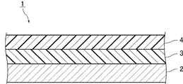
- FIG. 1 is a cross-sectional view schematically showing a laminate according to an embodiment of the present invention.
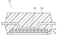
- FIG. 2 is a cross-sectional view schematically showing a power semiconductor module component obtained by the method for manufacturing a power semiconductor module component according to an embodiment of the present invention.
- the laminated body according to the present invention includes a thermal conductor having a thermal conductivity of 10 W / m ⁇ K or more, and a first insulation that is laminated on the surface of the thermal conductor and is a semi-cured product or a cured product. And a second insulating layer which is laminated on the surface of the first insulating layer opposite to the heat conductor side and which is an uncured or semi-cured material.
- the first insulating layer includes an inorganic filler having a thermal conductivity of 10 W / m ⁇ K or more in an amount of 86 wt% or more and less than 97 wt%.
- the second insulating layer contains an inorganic filler at 67 wt% or more and less than 95 wt%.
- the curing rate of the first insulating layer is 50% or more, the curing rate of the second insulating layer is less than 80%, and the curing rate of the first insulating layer is that of the second insulating layer. Greater than
- the thermal conductivity of the insulating layer can be increased by adopting the above configuration in the laminate according to the present invention. Further, by laminating a conductive layer on the surface of the second insulating layer opposite to the first insulating layer side, adhesion between the insulating layer and the conductive layer can be improved.
- the above-described laminate is used.
- a conductive layer is stacked on the surface of the stacked body opposite to the first insulating layer side using the stacked body.
- a step of curing the second insulating layer, and a step of curing the first insulating layer when the first insulating layer is a semi-cured material, and the thermal conductor and the first A step of embedding the insulating layer, the second insulating layer, and the conductive layer in a mold resin.
- a power semiconductor module component having a high thermal conductivity of the insulating layer and a high adhesiveness between the insulating layer and the conductive layer can be obtained.
- the first insulating layer contains an inorganic filler having a thermal conductivity of 10 W / m ⁇ K or more in an amount of 86 wt% or more and less than 97 wt%
- the second insulating layer contains an inorganic filler 67 Inclusion in an amount of not less than 95% by weight can effectively increase the thermal conductivity of the entire insulating layer while maintaining high adhesion between the second insulating layer, which is a cured product, and the conductive layer. it can.
- the curing rate of the first insulating layer is 50% or more
- the curing rate of the second insulating layer is less than 80%
- the curing rate of the first insulating layer is the second insulating layer.
- the first insulating layer may be a semi-cured product that has been cured and can be further cured, or a cured product that has been cured.
- the second insulating layer may be an uncured material that is not cured at all and can be cured, or may be a semi-cured material that has been cured and can be further cured.
- the curing rate of the first insulating layer that is a semi-cured product or a cured product before curing in the laminate is 50% or more, more preferably 60% or more, and still more preferably 70% or more.
- the curing rate of the first insulating layer may be 80% or more, 90% or more, 95% or more, or 100%.
- the curing rate of the second insulating layer which is an uncured or semi-cured product before curing in the laminate, is less than 80%.
- the curing rate of the second insulating layer is preferably 1% or more, may be 10% or more, and may be 20% or more.
- the curing rate of the second insulating layer may be less than 70%, less than 60%, or less than 50%.
- the curing rate of the first insulating layer is It is preferably 1% or more, more preferably 5% or more, and still more preferably 10% or more larger than the curing rate of the insulating layer 2.
- the curing rate of the first insulating layer may be 20% or more larger than the curing rate of the second insulating layer, or 30% or more.
- the curing rate of the first and second insulating layers can be obtained by measuring the heat of curing when the uncured insulating layer is heated.
- a differential scanning calorimetry (DSC) apparatus (“DSC7020” manufactured by SII Nanotechnology) or the like is used.
- the curing rates of the first and second insulating layers are measured as follows.
- the temperature of the first insulating layer or the second insulating layer is increased to 180 ° C. at a measurement start temperature of 30 ° C. and a heating rate of 8 ° C./min, and held for 1 hour.
- the amount of heat generated when the first insulating layer or the second insulating layer is cured at this temperature rise (hereinafter referred to as heat amount A) is measured.
- a curable composition for forming the first insulating layer or the second insulating layer was applied to a release PET (polyethylene terephthalate) sheet having a thickness of 50 ⁇ m so as to have a thickness of 80 ⁇ m.
- a non-cured and uncured insulating layer is prepared in the same manner as the first insulating layer or the second insulating layer in the above laminate except that it is dried for 1 hour under a room temperature vacuum of 0.01 atm. .
- the amount of heat (hereinafter, referred to as the amount of heat B) generated when the temperature is hardened is measured in the same manner as in the measurement of the amount of heat A. From the obtained heat quantity A and heat quantity B, the curing rates of the first and second insulating layers are obtained by the following formula.
- Curing rate (%) [1- (heat amount A / heat amount B)] ⁇ 100
- the viscosity ⁇ at 130 ° C. of the second insulating layer which is an uncured or semi-cured material before curing in the laminate is preferably 1000 Pa ⁇ s or more, more preferably 5000 Pa ⁇ s or more, and still more preferably 6000 Pa ⁇ s. s or more, preferably 20000 Pa ⁇ s or less, more preferably 15000 Pa ⁇ s or less.
- the viscosity ⁇ is not less than the above lower limit and not more than the above upper limit, the thickness of the second insulating layer hardly changes during adhesion of the conductive layer, the withstand voltage of the cured product is stabilized, and the cured product is deformed to some extent. The adhesion between the second insulating layer and the conductive layer is even higher.
- the viscosity ⁇ indicates the viscosity at 130 ° C. when the second insulating layer, which is an uncured or semi-cured product before curing, is heated from 23 ° C. at a temperature rising rate of 8 ° C./min.
- the reason why the temperature defining the viscosity ⁇ is 130 ° C. is that the temperature suitable for bonding with the conductive layer is around 130 ° C.
- VAR-100 manufactured by Rheologicala Instruments
- the first insulating layer is a cured product.
- the first insulating layer which is a cured product, has a coefficient of thermal expansion of 20 ppm / ° C. or less, and when the first insulating layer is a semi-cured product, the first cured product is a cured product.
- the thermal expansion coefficient of the insulating layer is preferably 20 ppm / ° C. or less.
- the first insulating layer which is a cured product
- the coefficient of thermal expansion of is preferably 3 ppm / ° C. or higher, more preferably 18 ppm / ° C. or lower.
- thermomechanical analyzer (TMA / SS7000” manufactured by SII Nanotechnology) or the like is used.
- the first insulating layer in the laminate is a semi-cured product
- the first insulating layer which is a cured product for measuring the coefficient of thermal expansion
- the layer is preferably obtained by curing at 200 ° C. for 1 hour.
- the ratio of the thickness of the second insulating layer to the thickness of the first insulating layer is preferably 0.03 or more, more preferably 0.00. 1 or more, more preferably 0.3 or more, preferably 10 or less, more preferably 3 or less, still more preferably 1 or less.
- the thickness of the first insulating layer is the first thickness.
- the ratio of the insulating layer to the thickness is particularly preferably 0.3 or more and 1 or less.
- the total thickness of the first and second insulating layers is not particularly limited.
- the total thickness of the first and second insulating layers is preferably 80 ⁇ m or more, more preferably 100 ⁇ m or more, preferably 200 ⁇ m or less, more preferably 170 ⁇ m or less.
- the total thickness of the first and second insulating layers is equal to or more than the above lower limit, the heat dissipation in the entire insulating layer, the adhesiveness between the second insulating layer and the conductive layer, which is a cured product, and the entire insulating layer The withstand voltage is improved in a well-balanced manner.
- the first insulating layer is preferably formed using a curable compound (A) and a curing agent (B).
- the first insulating layer is preferably formed using a first curable composition containing a curable compound (A) and a curing agent (B). From the viewpoint of forming a first insulating layer having good curability, the first insulating layer is formed using a curable compound (A1) having a cyclic ether group and a curing agent (B). Is preferred.
- the first insulating layer contains an inorganic filler (C). It is preferable that a 1st curable composition contains an inorganic filler (C).
- the inorganic filler (C) contained in the first insulating layer and the first curable composition is an inorganic filler having a thermal conductivity of 10 W / m ⁇ K or more.
- the second insulating layer is preferably formed using a curable compound (A) and a curing agent (B). It is preferable that the said 2nd insulating layer is formed using the 2nd curable composition containing a sclerosing
- the second insulating layer contains an inorganic filler (C). Accordingly, the second curable composition preferably contains an inorganic filler (C).
- the inorganic filler (C) contained in the second insulating layer and the second curable composition may be an inorganic filler having a thermal conductivity of 10 W / m ⁇ K or more, and a thermal conductivity of 10 W.
- the inorganic filler may be less than / m ⁇ K.
- the thermal conductivity of the inorganic filler (C) contained in the second insulating layer and the second curable composition is 10 W / m ⁇ K. The above is preferable.
- Each of the first and second insulating layers is preferably formed using a curable compound (A).
- Each of the first and second curable compositions contains a curable compound (A).
- the curable compound (A) is preferably a thermosetting compound.
- the curable compound (A) is preferably a curable compound (A1) having a cyclic ether group. Examples of the cyclic ether group include an epoxy group and an oxetanyl group.
- the curable compound (A1) having a cyclic ether group is preferably a curable compound having an epoxy group or an oxetanyl group.
- the curable compound (A) is cured by the action of the curing agent (B).
- curable compound (A) used for each of the first and second insulating layers only one type may be used, or two or more types may be used in combination.
- the curable compound (A) used for the first insulating layer and the curable compound (A) used for the second insulating layer may be the same or different.
- the curable compound (A1) may contain an epoxy compound (A1a) having an epoxy group, or may contain an oxetane compound (A1b) having an oxetanyl group.
- the curable compound (A) preferably has an aromatic skeleton from the viewpoint of further improving the heat resistance and voltage resistance of an insulating layer that is a cured product (hereinafter sometimes simply referred to as a cured product).
- the curable compound (A) used for the first insulating layer preferably contains a curable compound having a polycyclic aromatic skeleton. More preferably, it contains a curable compound having a cyclic ether group and a polycyclic aromatic skeleton.
- polycyclic aromatic skeleton examples include a naphthalene skeleton, an anthracene skeleton, a xanthene skeleton, a fluorene skeleton, and a biphenyl skeleton. From the viewpoint of further improving the thermal conductivity and voltage resistance of the cured product, the polycyclic aromatic skeleton is preferably a biphenyl skeleton.
- the content of the curable compound having a polycyclic aromatic skeleton in the total 100% by weight of the curable compound (A) is preferably 30% by weight or more, more preferably 50% by weight or more, and further preferably 60% by weight. That's it.
- the total amount of the curable compound (A) may be a curable compound having a polycyclic aromatic skeleton.
- the epoxy compound (A1a) having an epoxy group examples include an epoxy monomer having a bisphenol skeleton, an epoxy monomer having a dicyclopentadiene skeleton, an epoxy monomer having a naphthalene skeleton, an epoxy monomer having an adamantane skeleton, and an epoxy having a fluorene skeleton.
- the monomer examples include an epoxy monomer having a biphenyl skeleton, an epoxy monomer having a bi (glycidyloxyphenyl) methane skeleton, an epoxy monomer having a xanthene skeleton, an epoxy monomer having an anthracene skeleton, and an epoxy monomer having a pyrene skeleton.
- These hydrogenated products or modified products may be used.
- an epoxy compound (A1a) only 1 type may be used and 2 or more types may be used together.
- Examples of the epoxy monomer having a bisphenol skeleton include an epoxy monomer having a bisphenol A type, bisphenol F type, or bisphenol S type bisphenol skeleton.
- Examples of the epoxy monomer having a dicyclopentadiene skeleton include dicyclopentadiene dioxide and a phenol novolac epoxy monomer having a dicyclopentadiene skeleton.
- Examples of the epoxy monomer having a naphthalene skeleton include 1-glycidylnaphthalene, 2-glycidylnaphthalene, 1,2-diglycidylnaphthalene, 1,5-diglycidylnaphthalene, 1,6-diglycidylnaphthalene, 1,7-diglycidyl.
- Examples include naphthalene, 2,7-diglycidylnaphthalene, triglycidylnaphthalene, and 1,2,5,6-tetraglycidylnaphthalene.
- Examples of the epoxy monomer having an adamantane skeleton include 1,3-bis (4-glycidyloxyphenyl) adamantane and 2,2-bis (4-glycidyloxyphenyl) adamantane.
- Examples of the epoxy monomer having a fluorene skeleton include 9,9-bis (4-glycidyloxyphenyl) fluorene, 9,9-bis (4-glycidyloxy-3-methylphenyl) fluorene, and 9,9-bis (4- Glycidyloxy-3-chlorophenyl) fluorene, 9,9-bis (4-glycidyloxy-3-bromophenyl) fluorene, 9,9-bis (4-glycidyloxy-3-fluorophenyl) fluorene, 9,9-bis (4-Glycidyloxy-3-methoxyphenyl) fluorene, 9,9-bis (4-glycidyloxy-3,5-dimethylphenyl) fluorene, 9,9-bis (4-glycidyloxy-3,5-dichlorophenyl) Fluorene and 9,9-bis (4-glycidyloxy-3,5-dibromophenyl) Fluorene,
- Examples of the epoxy monomer having a biphenyl skeleton include 4,4'-diglycidylbiphenyl and 4,4'-diglycidyl-3,3 ', 5,5'-tetramethylbiphenyl.
- Examples of the epoxy monomer having a bi (glycidyloxyphenyl) methane skeleton include 1,1′-bi (2,7-glycidyloxynaphthyl) methane, 1,8′-bi (2,7-glycidyloxynaphthyl) methane, 1,1′-bi (3,7-glycidyloxynaphthyl) methane, 1,8′-bi (3,7-glycidyloxynaphthyl) methane, 1,1′-bi (3,5-glycidyloxynaphthyl) methane 1,8'-bi (3,5-glycidyloxynaphthyl) methane, 1,2'-bi (2,7-glycidyloxynaphthyl) methane, 1,2'-bi (3,7-glycidyloxynaphthyl) And methane and 1,2
- Examples of the epoxy monomer having a xanthene skeleton include 1,3,4,5,6,8-hexamethyl-2,7-bis-oxiranylmethoxy-9-phenyl-9H-xanthene.
- oxetane compound (A1b) having an oxetanyl group include, for example, 4,4′-bis [(3-ethyl-3-oxetanyl) methoxymethyl] biphenyl, 1,4-benzenedicarboxylate bis [(3- Ethyl-3-oxetanyl) methyl] ester, 1,4-bis [(3-ethyl-3-oxetanyl) methoxymethyl] benzene, and oxetane-modified phenol novolac.
- an oxetane compound (A1b) only 1 type may be used and 2 or more types may be used together.
- the curable compound (A) preferably has two or more cyclic ether groups.
- the content of the curable compound having two or more cyclic ether groups in the total 100% by weight of the curable compound (A) is preferably 70% by weight or more. More preferably, it is 80% by weight or more and 100% by weight or less.
- the content of the curable compound having two or more cyclic ether groups in the total 100% by weight of the curable compound (A) may be 10% by weight or more and 100% by weight or less.
- the entire curable compound (A) may be a curable compound having two or more cyclic ether groups.
- the molecular weight of the curable compound (A) is preferably less than 10,000.
- the molecular weight of the curable compound (A) is preferably 200 or more, more preferably 1200 or less, still more preferably 600 or less, and particularly preferably 550 or less.
- the adhesiveness of the surface of the insulating layer is lowered, and the handleability of the laminate is further enhanced.
- the molecular weight of the curable compound (A) is not more than the above upper limit, the adhesiveness of the cured product is further enhanced. Furthermore, the cured product is hard and hard to be brittle, and the adhesiveness of the cured product is further enhanced.
- the molecular weight in the curable compound (A) means a molecular weight that can be calculated from the structural formula when it is not a polymer and when the structural formula can be specified. Means weight average molecular weight.
- the content of the curable compound (A) is preferably 50% in a total of 100% by weight of the total resin components (hereinafter sometimes abbreviated as “total resin component X1”) contained in the first curable composition. % Or more, more preferably 60% by weight or more, preferably 99.5% by weight or less, more preferably 99% by weight or less, and still more preferably 98% by weight or less.
- total resin component X1 refers to the total of the curable compound (A), the curing agent (B), and other resin components added as necessary.
- the inorganic filler (C) is not included in all the resin components X1.
- the content of the curable compound (A) is preferably 50% in a total of 100% by weight of the total resin components (hereinafter sometimes abbreviated as “total resin component X2”) contained in the second curable composition. % Or more, more preferably 60% by weight or more, preferably 99.5% by weight or less, more preferably 99% by weight or less, and still more preferably 98% by weight or less.
- total resin component X2 total resin component contained in the second curable composition.
- the total resin component X2 refers to the total of the curable compound (A), the curing agent (B), and other resin components added as necessary.
- the inorganic filler (C) is not included in all the resin components X2.
- the resin component is a non-volatile component and refers to a component that does not volatilize during molding or heating of the curable composition or the insulating layer.
- the resin component is a solid content
- the solid content is a non-volatile content and refers to a component that does not volatilize during molding or heating of the curable composition or the insulating layer.
- Each of the first and second insulating layers is preferably formed using a curing agent (B).
- Each of the first and second curable compositions contains a curing agent (B).
- the curing agent (B) is not particularly limited as long as the first and second curable compositions can be cured.
- the curing agent (B) is preferably a thermosetting agent.
- As the curing agent (B) used for each of the first and second insulating layers only one kind may be used, or two or more kinds may be used in combination.
- the curing agent (B) used for the first insulating layer and the curing agent (B) used for the second insulating layer may be the same or different.
- the curing agent (B) preferably has an aromatic skeleton or an alicyclic skeleton.
- the curing agent (B) preferably includes an amine curing agent (amine compound), an imidazole curing agent, a phenol curing agent (phenol compound) or an acid anhydride curing agent (acid anhydride), and includes an amine curing agent. More preferred.
- the acid anhydride curing agent includes an acid anhydride having an aromatic skeleton, a water additive of the acid anhydride or a modified product of the acid anhydride, or an acid anhydride having an alicyclic skeleton, It is preferable to include a water additive of an acid anhydride or a modified product of the acid anhydride.
- the curing agent (B) contains a basic curing agent. Is preferred.
- the curing agent (B) is an amine curing agent. Or it is more preferable that an imidazole hardening
- curing agent (B) contains both a dicyandiamide and an imidazole hardening
- the amine curing agent examples include dicyandiamide, an imidazole compound, diaminodiphenylmethane, and diaminodiphenylsulfone.
- the amine curing agent more preferably contains a dicyandiamide or an imidazole compound.
- the curing agent (B) preferably contains a curing agent having a melting point of 180 ° C. or higher, and an amine curing agent having a melting point of 180 ° C. or higher. It is more preferable to contain.
- imidazole curing agent examples include 2-undecylimidazole, 2-heptadecylimidazole, 2-methylimidazole, 2-ethyl-4-methylimidazole, 2-phenylimidazole, 2-phenyl-4-methylimidazole, and 1-benzyl.
- phenol curing agent examples include phenol novolak, o-cresol novolak, p-cresol novolak, t-butylphenol novolak, dicyclopentadiene cresol, polyparavinylphenol, bisphenol A type novolak, xylylene modified novolak, decalin modified novolak, poly ( And di-o-hydroxyphenyl) methane, poly (di-m-hydroxyphenyl) methane, and poly (di-p-hydroxyphenyl) methane.
- a phenol resin having a melamine skeleton, a phenol resin having a triazine skeleton, or a phenol resin having an allyl group is preferable.
- phenol curing agent Commercially available products of the phenol curing agent include MEH-8005, MEH-8010 and MEH-8015 (all of which are manufactured by Meiwa Kasei Co., Ltd.), YLH903 (manufactured by Mitsubishi Chemical), LA-7052, LA-7054, and LA-7751. LA-1356 and LA-3018-50P (all of which are manufactured by DIC), and PS6313 and PS6492 (all of which are manufactured by Gunei Chemical Co., Ltd.).
- Examples of the acid anhydride having an aromatic skeleton, a water additive of the acid anhydride, or a modified product of the acid anhydride include, for example, a styrene / maleic anhydride copolymer, a benzophenone tetracarboxylic acid anhydride, and a pyromellitic acid anhydride.
- Trimellitic anhydride 4,4'-oxydiphthalic anhydride, phenylethynyl phthalic anhydride, glycerol bis (anhydrotrimellitate) monoacetate, ethylene glycol bis (anhydrotrimellitate), methyltetrahydroanhydride
- Examples include phthalic acid, methylhexahydrophthalic anhydride, and trialkyltetrahydrophthalic anhydride.
- Examples of commercially available acid anhydrides having an aromatic skeleton, water additives of the acid anhydrides, or modified products of the acid anhydrides include SMA Resin EF30, SMA Resin EF40, SMA Resin EF60, and SMA Resin EF80.
- the acid anhydride having an alicyclic skeleton, a water additive of the acid anhydride, or a modified product of the acid anhydride is an acid anhydride having a polyalicyclic skeleton, a water additive of the acid anhydride, or the A modified product of an acid anhydride, or an acid anhydride having an alicyclic skeleton obtained by addition reaction of a terpene compound and maleic anhydride, a water additive of the acid anhydride, or a modified product of the acid anhydride It is preferable. By using these curing agents, the flexibility of the cured product and the moisture resistance and adhesion of the cured product are further increased.
- Examples of the acid anhydride having an alicyclic skeleton, a water addition of the acid anhydride, or a modified product of the acid anhydride include methyl nadic acid anhydride, acid anhydride having a dicyclopentadiene skeleton, and the acid anhydride And the like.
- Examples of commercially available acid anhydrides having the alicyclic skeleton, water additions of the acid anhydrides, or modified products of the acid anhydrides include Jamaicacid HNA and Ricacid HNA-100 (all of which are manufactured by Shin Nippon Rika Co., Ltd.) , And EpiCure YH306, EpiCure YH307, EpiCure YH308H, EpiCure YH309 (all of which are manufactured by Mitsubishi Chemical Corporation) and the like.
- the curing agent (B) is also preferably methyl nadic acid anhydride or trialkyltetrahydrophthalic anhydride. Use of methyl nadic anhydride or trialkyltetrahydrophthalic anhydride increases the water resistance of the cured product.
- the content of the curing agent (B) is preferably 0.5% by weight or more, more preferably 1% by weight or more in the total 100% by weight of all the resin components X1 contained in the first curable composition. , Preferably 50% by weight or less, more preferably 40% by weight or less.
- the content of the curing agent (B) is not less than the above lower limit, it is easy to sufficiently cure the first curable composition.
- the content of the curing agent (B) is not more than the above upper limit, it is difficult to generate an excessive curing agent (B) that does not participate in curing. For this reason, the heat resistance and adhesiveness of hardened
- the content of the curing agent (B) is preferably 0.5% by weight or more, more preferably 1% by weight or more. , Preferably 50% by weight or less, more preferably 40% by weight or less. It is easy to fully harden a 2nd curable composition as content of a hardening
- Each of the first and second insulating layers contains an inorganic filler (C).
- the thermal conductivity of the inorganic filler (C) contained in the first insulating layer is 10 W / m ⁇ K or more.
- Each of the first and second curable compositions preferably contains an inorganic filler (C).
- the inorganic filler (C) contained in the first curable composition has a thermal conductivity of 10 W / m ⁇ K or more.
- the use of the inorganic filler (C) increases the thermal conductivity of the cured product. As a result, the thermal conductivity of the cured product is increased.
- the inorganic filler (C) used for each of the first and second insulating layers only one kind may be used, or two or more kinds may be used in combination.
- the inorganic filler (C) used for the first insulating layer and the inorganic filler (C) used for the second insulating layer may be the same or different.
- the thermal conductivity of the inorganic filler (C) contained in the first insulating layer and the first curable composition is preferably 15 W / m ⁇ K or more. More preferably, it is 20 W / m ⁇ K or more.
- the thermal conductivity of the inorganic filler (C) contained in the second insulating layer and the second curable composition is preferably 10 W / m ⁇ K or more. More preferably, it is 15 W / m ⁇ K or more, and further preferably 20 W / m ⁇ K or more.
- the upper limit of the thermal conductivity of the inorganic filler (C) is not particularly limited. Inorganic fillers having a thermal conductivity of about 300 W / m ⁇ K are widely known, and inorganic fillers having a thermal conductivity of about 200 W / m ⁇ K are easily available.
- the inorganic filler (C) is preferably at least one selected from the group consisting of alumina, synthetic magnesite, crystalline silica, boron nitride, aluminum nitride, silicon nitride, silicon carbide, zinc oxide and magnesium oxide, More preferably, it is at least one selected from the group consisting of alumina, crystalline silica, boron nitride and aluminum nitride. Use of these preferable inorganic fillers further increases the thermal conductivity of the cured product.
- the inorganic filler contained in the first insulating layer and the inorganic filler contained in the second insulating layer are respectively alumina, It is preferably at least one selected from the group consisting of crystalline silica, boron nitride and aluminum nitride.
- the inorganic filler contained in the first insulating layer is at least one selected from the group consisting of alumina, crystalline silica, and boron nitride. Is also preferable.
- the inorganic filler contained in the second insulating layer may be at least one selected from the group consisting of alumina, crystalline silica, and boron nitride.
- the inorganic filler (C) is more preferably at least one selected from the group consisting of spherical alumina, crushed alumina, crystalline silica, boron nitride, aggregated particles, and spherical aluminum nitride. Use of these preferable fillers further increases the thermal conductivity of the cured product.
- the boron nitride and the aggregated particles are preferably boron nitride and boron nitride aggregated particles that are not aggregated particles.
- the inorganic filler (C) preferably contains an inorganic filler having a new Mohs hardness of 12 or less.
- the new Mohs hardness of the inorganic filler having the new Mohs hardness of 12 or less is more preferably 9 or less.
- Use of an inorganic filler having a new Mohs hardness of not more than the above upper limit further increases the workability of the cured product.
- the inorganic filler (C) is preferably at least one selected from the group consisting of synthetic magnesite, crystalline silica, zinc oxide, and magnesium oxide.
- the new Mohs hardness of these inorganic fillers is 9 or less.
- the inorganic filler (C) may contain a spherical filler (spherical filler), may contain a crushed filler (crushed filler), or may contain a plate-like filler (plate-like filler). Good. It is particularly preferable that the inorganic filler (C) includes a spherical filler. Since spherical fillers can be filled at high density, the use of spherical fillers further increases the thermal conductivity of the cured product.
- Crushed filler may be mentioned as the crushed filler.
- the crushing filler is obtained, for example, by crushing a lump-like inorganic substance using a uniaxial crusher, a biaxial crusher, a hammer crusher, a ball mill, or the like.
- the filler in the insulating layer tends to be bridged or have a structure in which the filler is effectively brought into close proximity. Therefore, the thermal conductivity of the cured product is further increased.
- the crushing filler is cheap compared with a normal filler. For this reason, the cost of a laminated body becomes low by use of a crushing filler.
- the average particle size of the crushed filler is preferably 12 ⁇ m or less, more preferably 10 ⁇ m or less, and preferably 1 ⁇ m or more.
- the crushed filler can be dispersed with high density in the first and second curable compositions, and the withstand voltage of the cured product is further improved. Get higher.
- the average particle diameter of the crushed filler is not less than the above lower limit, it becomes easy to fill the crushed filler with high density.
- the aspect ratio of the crushed filler is not particularly limited.
- the aspect ratio of the crushed filler is preferably 1.5 or more, and preferably 20 or less. Fillers with an aspect ratio of less than 1.5 are relatively expensive and increase the cost of the laminate. When the aspect ratio is 20 or less, filling of the crushed filler is easy.
- the aspect ratio of the crushed filler can be determined, for example, by measuring the crushed surface of the filler using a digital image analysis particle size distribution measuring device (“FPA” manufactured by Nippon Lucas).
- FPA digital image analysis particle size distribution measuring device
- the average particle diameter of the spherical filler is preferably 0.1 ⁇ m or more, and preferably 40 ⁇ m or less.
- the average particle size is 0.1 ⁇ m or more, the inorganic filler (C) can be easily filled at a high density.
- the average particle size is 40 ⁇ m or less, the voltage resistance of the cured product is further enhanced.
- the above-mentioned “average particle diameter” is an average particle diameter obtained from a volume average particle size distribution measurement result measured with a laser diffraction particle size distribution measuring apparatus.
- the average major axis of the plate-like filler is preferably 0.1 ⁇ m or more, more preferably 0.5 ⁇ m or more, further preferably 1 ⁇ m or more, preferably 10 ⁇ m or less, more preferably 9 ⁇ m or less.
- the average major axis of the plate-like filler is not less than the above lower limit and not more than the above upper limit, a plurality of inorganic fillers can easily come into contact with each other. For this reason, the heat conductivity of hardened
- cured material becomes it high that the average major axis of a plate-shaped filler is below the said upper limit.
- the average thickness of the plate filler is preferably 100 nm or more. When the thickness of the plate filler is not less than the above lower limit, the thermal conductivity of the cured product is further increased.
- the aspect ratio of the plate-like filler is preferably 2 or more, more preferably 3 or more, preferably 50 or less, more preferably 45 or less. When the aspect ratio of the plate filler is not more than the above upper limit, the plate filler can be easily filled.
- the aspect ratio of the plate filler is more preferably in the range of 3 to 45.
- the plate filler is preferably at least one of alumina and boron nitride. In this case, the thermal conductivity of the cured product is further increased.
- the inorganic filler (C) contained in the first insulating layer preferably contains a plate-like filler.
- the inorganic filler (C) contained in the first insulating layer preferably contains a crushed filler or a spherical filler and a plate-like filler.
- the content of the plate-like filler is preferably less than 50% by weight, more preferably less than 30% by weight, and still more preferably less than 10% by weight.
- the inorganic filler (C) contained in the first insulating layer includes a crushed filler or a spherical filler and a plate-like filler
- the first insulating layer comprises a crushed filler, a spherical filler and a plate.
- the filler is preferably contained in a weight ratio of 9.5: 0.5 to 5: 5, more preferably 9: 1 to 7: 3.
- the maximum particle size of the inorganic filler (C) is preferably 70 ⁇ m or less, more preferably 50 ⁇ m or less.
- the maximum particle diameter of the said crushing filler and the said plate-shaped filler means the major axis of the largest particle.
- the maximum particle size of the inorganic filler is determined by measuring the maximum particle size when 100 inorganic fillers are observed using, for example, a digital image analysis type particle size distribution measuring apparatus (“FPA” manufactured by Nippon Lucas). Is possible.
- FPA digital image analysis type particle size distribution measuring apparatus
- the content of the inorganic filler (C) is 86% by weight or more and less than 97% by weight. In 100% by weight of the first curable composition, the content of the inorganic filler (C) is preferably 86% by weight or more and less than 97% by weight.
- the cured state of the first insulating layer that is a cured product is It becomes better and the thermal conductivity is considerably higher.
- the content of the inorganic filler (C) is 67% by weight or more and less than 95% by weight. In 100% by weight of the second curable composition, the content of the inorganic filler (C) is preferably 67% by weight or more and less than 95% by weight.
- the cured state of the second insulating layer that is a cured product is The adhesion between the second insulating layer, which is a cured product, and the conductive layer becomes considerably high.
- an inorganic filler (100 wt% of the first insulating layer)
- the content of C) is preferably greater than the content of the inorganic filler (C) in 100% by weight of the second insulating layer, more preferably 1% by weight or more, and more preferably 5% by weight or more. Preferably, it is more than 10% by weight.
- the content of the inorganic filler (C) in 100% by weight of the insulating layer) is preferably 0.7 or more, and preferably 0.95 or less.
- At least one of the first and second insulating layers preferably includes a flame retardant.
- the flame retardant preferably contains a phosphorus compound.
- the first insulating layer may contain a phosphorus compound
- the second insulating layer may contain a phosphorus compound
- both the first and second insulating layers contain a phosphorus compound. May be.
- the said phosphorus compound only 1 type may be used and 2 or more types may be used together.
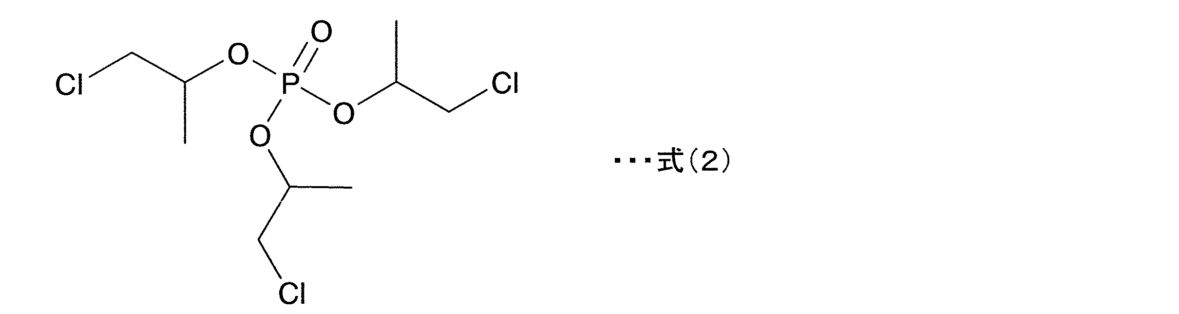
- the phosphorus compound is preferably a phosphorus compound represented by the following formula (1) or the following formula (2). Therefore, it is preferable that at least one of the first and second insulating layers contains a phosphorus compound represented by the following formula (1) or the following formula (2). At least one of the first and second insulating layers preferably contains triphenylphosphine or trischloroethyl phosphate.
- the content of the phosphorus compound in 100% by weight of the first insulating layer is preferably 0.5% by weight or more, more preferably 1% by weight or more, preferably 20% by weight or less, more preferably 15% by weight or less. is there.
- the content of the phosphorus compound in 100% by weight of the second insulating layer is preferably 0.5% by weight or more, more preferably 1% by weight or more, preferably 20% by weight or less, more preferably 15% by weight or less. is there.
- the content of the phosphorus compound is preferably 0.5% by weight or more, more preferably 1% by weight or more, preferably 20% by weight or less, more preferably in 100% by weight of the total of the first and second insulating layers. 15% by weight or less.
- the first and second insulating layers and the first and second curable compositions may include a polymer having a weight average molecular weight of 10,000 or more. As for this polymer, only 1 type may be used and 2 or more types may be used together.
- a curable resin such as a thermoplastic resin and a thermosetting resin can be used.
- the polymer is preferably a curable resin.
- thermoplastic resin and thermosetting resin are not particularly limited.
- the thermoplastic resin is not particularly limited, and examples thereof include styrene resin, phenoxy resin, phthalate resin, thermoplastic urethane resin, polyamide resin, thermoplastic polyimide resin, ketone resin, and norbornene resin.
- the thermosetting resin is not particularly limited, and examples thereof include amino resins, phenol resins, thermosetting urethane resins, epoxy resins, thermosetting polyimide resins, and amino alkyd resins. Examples of the amino resin include urea resin and melamine resin.
- the polymer is a styrene resin, phenoxy resin or epoxy resin. It is preferable that it is a phenoxy resin or an epoxy resin, more preferably a phenoxy resin.
- a phenoxy resin or an epoxy resin further increases the heat resistance of the cured product.
- use of a phenoxy resin further lowers the elastic modulus of the cured product and further improves the cold-heat cycle characteristics of the cured product.
- the polymer may not have a cyclic ether group such as an epoxy group.
- styrene resin specifically, a homopolymer of a styrene monomer, a copolymer of a styrene monomer and an acrylic monomer, or the like can be used. Of these, a styrene polymer having a styrene-glycidyl methacrylate structure is preferred.
- styrene monomer examples include styrene, o-methyl styrene, m-methyl styrene, p-methyl styrene, p-methoxy styrene, p-phenyl styrene, p-chloro styrene, p-ethyl styrene, pn- Butyl styrene, p-tert-butyl styrene, pn-hexyl styrene, pn-octyl styrene, pn-nonyl styrene, pn-decyl styrene, pn-dodecyl styrene, 2,4-dimethyl Examples include styrene and 3,4-dichlorostyrene.
- the phenoxy resin is specifically a resin obtained by reacting, for example, an epihalohydrin and a divalent phenol compound, or a resin obtained by reacting a divalent epoxy compound and a divalent phenol compound.
- the phenoxy resin comprises a bisphenol A skeleton, a bisphenol F skeleton, a bisphenol A / F mixed skeleton, a naphthalene skeleton, a fluorene skeleton, a biphenyl skeleton, an anthracene skeleton, a pyrene skeleton, a xanthene skeleton, an adamantane skeleton, and a dicyclopentadiene skeleton. It is preferred to have at least one skeleton selected from the group.
- the phenoxy resin preferably has at least one skeleton selected from the group consisting of a bisphenol A skeleton, a bisphenol F skeleton, a bisphenol A / F mixed skeleton, a naphthalene skeleton, a fluorene skeleton, and a biphenyl skeleton.
- it has at least one skeleton of a fluorene skeleton and a biphenyl skeleton.
- Use of the phenoxy resin having these preferable skeletons further increases the heat resistance of the cured product.
- the epoxy resin is an epoxy resin other than the phenoxy resin.
- the epoxy resins include styrene skeleton-containing epoxy resins, bisphenol A type epoxy resins, bisphenol F type epoxy resins, bisphenol S type epoxy resins, phenol novolac type epoxy resins, biphenol type epoxy resins, naphthalene type epoxy resins, and fluorene type epoxy resins. , Phenol aralkyl type epoxy resin, naphthol aralkyl type epoxy resin, dicyclopentadiene type epoxy resin, anthracene type epoxy resin, epoxy resin having adamantane skeleton, epoxy resin having tricyclodecane skeleton, and epoxy resin having triazine nucleus in skeleton Etc.
- the polymer is included in the resin component.
- the first and second insulating layers and the first and second curable compositions may contain rubber particles. Use of the rubber particles increases the stress relaxation property and flexibility of the cured product.
- the rubber particles are included in the resin component.
- the first and second insulating layers and the first and second curable compositions may contain a dispersant. Use of the dispersant further increases the thermal conductivity and voltage resistance of the cured product.
- the dispersant preferably has a functional group containing a hydrogen atom having hydrogen bonding properties.
- the thermal conductivity and voltage resistance of the cured product are further enhanced.
- the pKa of the functional group containing a hydrogen atom having hydrogen bonding property is preferably 2 or more, more preferably 3 or more, preferably 10 or less, more preferably 9 or less.
- the pKa of the functional group is not less than the lower limit, the acidity of the dispersant does not become too high. Therefore, the storage stability of the 1st, 2nd curable composition and the 1st, 2nd insulating layer before hardening becomes still higher.
- the pKa of the functional group is not more than the above upper limit, the function as the dispersant is sufficiently achieved, and the thermal conductivity and voltage resistance of the cured product are further enhanced.
- the functional group containing a hydrogen atom having hydrogen bonding properties is preferably a carboxyl group or a phosphate group. In this case, the thermal conductivity and voltage resistance of the cured product are further increased.
- the dispersant examples include a polyester carboxylic acid, a polyether carboxylic acid, a polyacrylic carboxylic acid, an aliphatic carboxylic acid, a polysiloxane carboxylic acid, a polyester phosphoric acid, and a polyether type.
- examples thereof include phosphoric acid, polyacrylic phosphoric acid, aliphatic phosphoric acid, polysiloxane phosphoric acid, polyester phenol, polyether phenol, polyacrylic phenol, aliphatic phenol, and polysiloxane phenol.
- the said dispersing agent only 1 type may be used and 2 or more types may be used together.
- the content of the dispersant is preferably 0.01% by weight or more, more preferably 0.1% by weight or more, preferably 20% by weight. Below, more preferably 10% by weight or less.
- the content of the dispersant is not less than the above lower limit and not more than the upper limit, the aggregation of the inorganic filler (C) is suppressed, and the thermal conductivity and voltage resistance of the cured product are further enhanced.
- the dispersant is included in the resin component.
- the first and second insulating layers and the first and second curable compositions may contain a base material such as glass cloth, glass nonwoven fabric, and aramid nonwoven fabric.
- Each of the first and second insulating layers may be a prepreg, but is preferably not a prepreg.
- the first and second insulating layers and the first and second curable compositions preferably do not contain a base material, and particularly preferably do not contain glass cloth.
- the first and second insulating layers and the first and second curable compositions do not contain the base material, the thickness of the entire insulating layer is reduced, and the thermal conductivity of the cured product is further improved. It becomes higher, and various processing such as laser processing or drilling can be easily performed on the insulating layer as necessary.
- first and second insulating layers and the first and second curable compositions may include a silane coupling agent, an antioxidant, an ion scavenger, a tackifier, and a plasticizer as necessary.
- a thixotropic agent, a photosensitizer, a colorant and the like may be contained.
- the silane coupling agent is included in the resin component.
- the manufacturing method of the said laminated body is not specifically limited.
- the first curable composition described above is applied on a heat conductor by a solvent casting method or the like, and the first curable composition is allowed to proceed to be cured, thereby first insulation.
- the second curable composition described above is applied onto the first insulating layer by a solvent casting method or the like, and the curing of the second curable composition proceeds as necessary.
- the first curable composition is applied onto the release film by the solvent casting method or the like, and the first curable composition is cured.
- the second curable composition described above is applied onto the first insulating layer by a solvent cast method or the like, and the second curable composition is applied as necessary. After curing of the composition proceeds to form a second insulating layer to obtain a laminated film, the release film is peeled off, and the first and second insulating layers are removed.
- hardening of a 1st curable composition may be performed after application
- coating of a 2nd curable composition. Curing of the first curable composition may be performed before or after the first insulating layer is laminated on the thermal conductor.
- the first and second insulating layers may be formed by an extrusion method.
- the manufacturing method of the said laminated body is not limited to these methods.
- the thermal conductivity of the first insulating layer is preferably 3 W / m ⁇ K or more, more preferably 4 W / m ⁇ K or more, and further preferably 5 W / m ⁇ K or more.
- the thermal conductivity of the second insulating layer is preferably 1 W / m ⁇ K or more, more preferably 1.5 W / m ⁇ K or more, and further preferably 2 W / m ⁇ K or more.
- the dielectric breakdown voltage of the first and second insulating layers as a cured product is preferably 30 kV or more, more preferably 40 kV or more, still more preferably 50 kV or more, particularly preferably 80 kV or more, and most preferably 100 kV or more. .
- FIG. 1 An example of the laminated body which concerns on one Embodiment of this invention is shown with sectional drawing.
- a laminated body 1 shown in FIG. 1 includes a thermal conductor 2 having a thermal conductivity of 10 W / m ⁇ K or more, a first insulating layer 3 that is a semi-cured product or a cured product, and an uncured product or a semi-cured product. And a second insulating layer 4.
- the first insulating layer 3 is laminated on the surface of the heat conductor 2.
- the first insulating layer 3 only needs to be stacked on at least one surface of the heat conductor 2, and two first insulating layers may be stacked one on each side of the heat conductor. Good.
- the second insulating layer 4 is laminated on the surface of the first insulating layer 3 opposite to the heat conductor 2 side.
- the first insulating layer 3 includes an inorganic filler having a thermal conductivity of 10 W / m ⁇ K or more in an amount of 86 wt% or more and less than 97 wt%, and the second insulating layer 4 includes an inorganic filler of 67 wt%.
- the content is less than 95% by weight.
- the curing rate of the first insulating layer 3 is 50% or more, the curing rate of the second insulating layer 4 is less than 80%, and the curing rate of the first insulating layer 3 is that of the second insulating layer 4. Greater than cure rate.
- FIG. 2 is a cross-sectional view showing an example of a power semiconductor module component obtained by the method for manufacturing a power semiconductor module component according to an embodiment of the present invention.
- the second insulating layer 4 in the laminate 1 is an uncured product or a semi-cured product, whereas in the power semiconductor module component 11, the second insulating layer 4 is cured.
- the power semiconductor module component 11 includes a thermal conductor 2 having a thermal conductivity of 10 W / m ⁇ K or more, a first insulating layer 3 that is a cured product, a second insulating layer 4 that is a cured product, A conductive layer 12 and a mold resin 13 are provided.
- the conductive layer 12 is laminated on the surface of the second insulating layer 4 opposite to the first insulating layer 3 side.
- the thermal conductor 2, the first insulating layer 3, the second insulating layer 4, and the conductive layer 12 are embedded in the mold resin 13. Part of the conductive layer 12 is preferably exposed from the mold resin 13.
- the conductive layer 12 is laminated on the surface of the laminate 1 opposite to the first insulating layer 3 side of the second insulating layer 4, and then the second insulating layer 4 is cured. And when the 1st insulating layer 3 is a semi-hardened material, the 1st insulating layer 3 is hardened, Furthermore, the heat conductor 2, the 1st insulating layer 3, the 2nd insulating layer 4, and the conductive layer 12 Is embedded in the mold resin 13. At this time, it is preferable that the thermal conductor 2, the first insulating layer 3, the second insulating layer 4, and the conductive layer 12 are embedded in the mold resin 13 so that a part of the conductive layer 12 is exposed.
- the first and second insulating layers 3 and 4 are cured. Also good.
- the first and second insulating layers 3 and 4 may be cured when the mold resin 13 is cured.
- the laminate according to the present invention is preferably a laminate used for obtaining a power semiconductor module component.
- the use of the laminate is not limited to the power semiconductor module component described above.
- the first and second insulating layers are applied to each conductive layer such as a laminate or multilayer wiring board provided with copper circuits on both sides, a copper foil, a copper plate, a semiconductor element, or a semiconductor package.
- Various electric parts to which a metal body is bonded may be obtained.
- the laminate is suitably used for adhering a heat conductor to a conductive layer of a semiconductor device in which a semiconductor element is mounted on a substrate.
- the laminated body adheres a thermal conductor having a thermal conductivity of 10 W / m ⁇ K or more to a conductive layer of an electronic component device in which electronic component elements other than semiconductor elements are mounted on a substrate.
- a thermal conductor having a thermal conductivity of 10 W / m ⁇ K or more to a conductive layer of an electronic component device in which electronic component elements other than semiconductor elements are mounted on a substrate.
- the thermal conductor having a thermal conductivity of 10 W / m ⁇ K or more is not particularly limited.
- Examples of the heat conductor having a thermal conductivity of 10 W / m ⁇ K or more include aluminum, copper, alumina, beryllia, silicon carbide, silicon nitride, aluminum nitride, and a graphite sheet.
- the heat conductor whose said heat conductivity is 10 W / m * K or more is copper or aluminum. Copper or aluminum is excellent in heat dissipation.
- [Curing agent (B)] (1) Alicyclic skeleton acid anhydride (“MH-700” manufactured by Shin Nippon Rika Co., Ltd.) (2) Biphenyl skeleton phenolic resin (“MEH-7851-S” manufactured by Meiwa Kasei Co., Ltd.) (3) Diaminodiphenylmethane (melting point 90 ° C) (4) Dicyandiamide (melting point 208 ° C) (5) Isocyanur-modified solid dispersion type imidazole (“2MZA-PW” manufactured by Shikoku Kasei Co., Ltd., melting point 253 ° C.)
- TPP Triphenylphosphine
- TCEP Trischloroethyl phosphate
- Epoxysilane coupling agent (“KBE403” manufactured by Shin-Etsu Chemical Co., Ltd.)
- Example 1 A first curable composition for forming a first insulating layer, using a homodisper type stirrer, blending and kneading each component in the proportions shown in Table 1 below (the blending unit is parts by weight), and A second curable composition for forming a second insulating layer was prepared.
- the first curable composition was coated on a release PET sheet having a thickness of 50 ⁇ m and dried in an oven at 90 ° C. for 30 minutes to produce a first insulating layer having a thickness of 80 ⁇ m on the PET sheet.
- the second curable composition is coated on a 50 ⁇ m thick release PET sheet and dried in an oven at 90 ° C. for 30 minutes to produce a second insulating layer having a thickness of 80 ⁇ m on the PET sheet. did.
- the obtained first insulating layer was bonded onto a copper plate having a thickness of 0.5 mm using a thermal laminator and then cured at 200 ° C. for 1 hour (curing conditions for the first curable composition). Thereafter, the second insulating layer is bonded onto the first insulating layer using a thermal laminator, and then cured at 130 ° C. for 3 minutes (curing conditions for the second curable composition) to produce a laminate. did.
- an electrolytic copper foil having a thickness of 35 ⁇ m was pressed against the second insulating layer side of the laminate at a pressure of 1 MPa, and heated at 200 ° C. for 1 hour to obtain a laminate structure. Obtained.
- Examples 2 to 54 and Comparative Examples 1 to 7 The types and blending amounts of the components used in the first and second curable compositions, the curing conditions for the first and second curable compositions, the thicknesses of the first and second insulating layers, and a laminate are obtained.
- the first and second curable compositions were prepared in the same manner as in Example 1 except that the thickness of the copper plate used was as shown in Tables 1 to 12 below. Was made.
- Viscosity at 130 ° C. of second insulating layer which is uncured or semi-cured material before curing in laminate The second insulating layer of the laminate was processed into a disk shape having a diameter of 2 cm.
- a rotary dynamic viscoelasticity measuring device (“VAR-100” manufactured by Rheologicala Instruments)
- the viscosity of the second insulating layer at 130 ° C. is controlled by an oscillation strain control mode using a parallel plate with a diameter of 2 cm. The measurement was carried out while heating at 23 ° C. and a heating rate of 8 ° C./min under the conditions of an initial stress of 10 Pa, a frequency of 1 Hz, and a strain of 1%.
- Thermal conductivity The 1st insulating layer and 2nd insulating layer of the laminated body were taken out. The thermal conductivity of the first insulating layer and the thermal conductivity of the second insulating layer were measured using a thermal conductivity meter (“rapid thermal conductivity meter QTM-500” manufactured by Kyoto Electronics Industry Co., Ltd.).
- the first insulating layer in the laminate was cut into a size of 3 mm ⁇ 25 mm.
- the cured product was used as a test sample.
- the first insulating layer was a semi-cured product
- the first insulating layer was cured in an oven at 200 ° C. for 1 hour to prepare a test sample that was a cured product.
- TMA apparatus (“TMA / SS7000” manufactured by SII Nanotechnology Co., Ltd.)
- the obtained test sample was heated once to 320 ° C. at a temperature rising rate of 10 ° C./min, then cooled to ⁇ 45 ° C.
- the slope of the temperature-TMA line when the temperature was raised from ⁇ 45 ° C. to 130 ° C. at 10 ° C./min was measured, and the reciprocal thereof was calculated as the coefficient of thermal expansion at ⁇ 45 to 130 ° C.
- Dielectric breakdown voltage (withstand voltage)
- the first and second insulating layers of the laminate were taken out.
- the first and second insulating layers were cut into a size of 100 mm ⁇ 100 mm to obtain a test sample.
- the obtained test sample was cured in an oven at 200 ° C. for 1 hour to obtain an insulating layer as a cured product.
- a withstand voltage tester (“MODEL7473” manufactured by EXTECH Electronics)
- an AC voltage was applied between the insulating layers so that the voltage increased at a rate of 1 kV / sec.
- the voltage at which the insulating layer was broken was taken as the breakdown voltage.
- the laminated body is processed to a size of 10 mm ⁇ 500 mm, placed on a horizontal base with the copper plate side facing down, and the maximum and minimum heights of the top surface of the laminated body was evaluated as the warpage of the laminate.
- the warpage of the laminate was determined according to the following criteria.
- Warpage is less than 0.1 mm ⁇ : Warpage is 0.1 mm or more and less than 0.5 mm ⁇ : Warpage is 0.5 mm or more
- the laminated body was router-processed using a drill having a diameter of 2.0 mm ("RA series" manufactured by Union Tool Co., Ltd.) under conditions of a rotation speed of 30000 and a table feed speed of 0.5 m / min. The processing distance until the flash was generated was measured. Workability was evaluated according to the following criteria.
- the laminate was cured in an oven at 200 ° C. for 1 hour.
- the laminated body after curing was pressed from the side of the second insulating layer, which was a cured product, to a heating element with a smooth surface controlled to 60 ° C. of the same size at a pressure of 196 N / cm 2 .
- the surface temperature of the copper plate was measured by a thermocouple. The heat dissipation was determined according to the following criteria.
Landscapes
- Laminated Bodies (AREA)
- Cooling Or The Like Of Semiconductors Or Solid State Devices (AREA)
Abstract
Description
上記第1,第2の絶縁層はそれぞれ、硬化性化合物(A)を用いて形成されていることが好ましい。上記第1,第2の硬化性組成物はそれぞれ、硬化性化合物(A)を含む。硬化性化合物(A)は、熱硬化性化合物であることが好ましい。硬化性化合物(A)は、環状エーテル基を有する硬化性化合物(A1)であること好ましい。該環状エーテル基としては、エポキシ基及びオキセタニル基等が挙げられる。環状エーテル基を有する硬化性化合物(A1)は、エポキシ基又はオキセタニル基を有する硬化性化合物であることが好ましい。硬化性化合物(A)は、硬化剤(B)の作用により硬化する。第1,第2の絶縁層にそれぞれ用いる硬化性化合物(A)は、1種のみが用いられてもよく、2種以上が併用されてもよい。第1の絶縁層に用いる硬化性化合物(A)と第2の絶縁層に用いる硬化性化合物(A)とは同一であってもよく、異なっていてもよい。
上記第1,第2の絶縁層はそれぞれ、硬化剤(B)を用いて形成されていることが好ましい。上記第1,第2の硬化性組成物はそれぞれ、硬化剤(B)を含む。硬化剤(B)は、第1,第2の硬化性組成物を硬化させることが可能であれば特に限定されない。硬化剤(B)は、熱硬化剤であることが好ましい。第1,第2の絶縁層にそれぞれ用いる硬化剤(B)は、1種のみが用いられてもよく、2種以上が併用されてもよい。第1の絶縁層に用いる硬化剤(B)と第2の絶縁層に用いる硬化剤(B)とは同一であってもよく、異なっていてもよい。
上記第1,第2の絶縁層はそれぞれ、無機フィラー(C)を含む。上記第1の絶縁層に含まれている無機フィラー(C)の熱伝導率は10W/m・K以上である。上記第1,第2の硬化性組成物はそれぞれ、無機フィラー(C)を含むことが好ましい。上記第1の硬化性組成物に含まれている無機フィラー(C)の熱伝導率は10W/m・K以上である。無機フィラー(C)の使用により、硬化物の熱伝導性が高くなる。この結果、硬化物の熱伝導性が高くなる。上記第1,第2の絶縁層にそれぞれ用いる無機フィラー(C)は、1種のみが用いられてもよく、2種以上が併用されてもよい。上記第1の絶縁層に用いる無機フィラー(C)と上記第2の絶縁層に用いる無機フィラー(C)とは同一であってもよく、異なっていてもよい。
上記第1,第2の絶縁層の内の少なくとも一方は、難燃剤を含むことが好ましい。該難燃剤は、リン化合物を含むことが好ましい。リン化合物の使用により、硬化物の難燃性がより一層良好になる。上記第1の絶縁層が、リン化合物を含んでいてもよく、上記第2の絶縁層がリン化合物を含んでいてもよく、上記第1,第2の絶縁層の双方がリン化合物を含んでいてもよい。上記リン化合物は1種のみが用いられてもよく、2種以上が併用されてもよい。

上記第1,第2の絶縁層及び上記第1,第2の硬化性組成物は、重量平均分子量が10000以上であるポリマーを含んでいてもよい。該ポリマーは、1種のみが用いられてもよく、2種以上が併用されてもよい。
上記積層体の製造方法は特に限定されない。この製造方法として、例えば、熱伝導体上に、上述した第1の硬化性組成物を溶剤キャスト法等で塗工して、第1の硬化性組成物の硬化を進行させて第1の絶縁層を形成した後、該第1の絶縁層上に、上述した第2の硬化性組成物を溶剤キャスト法等で塗工して、必要に応じて第2の硬化性組成物の硬化を進行させて第2の絶縁層を形成する方法、並びに離型フィルム上に、上述した第1の硬化性組成物を溶剤キャスト法等で塗工して、第1の硬化性組成物の硬化を進行させて第1の絶縁層を形成した後、該第1の絶縁層上に、上述した第2の硬化性組成物を溶剤キャスト法等で塗工して、必要に応じて第2の硬化性組成物の硬化を進行させて第2の絶縁層を形成して積層フィルムを得た後、離型フィルムを剥離して、第1,第2の絶縁層を第1の絶縁層側から熱伝導体上に積層する方法等が挙げられる。また、第1の硬化性組成物の硬化は、第2の硬化性組成物の塗工の後に行われてもよい。第1の硬化性組成物の硬化は、第1の絶縁層が熱伝導体に積層される前に行われてもよく、積層された後に行われてもよい。また、第1,第2の絶縁層を、押出成形法により形成してもよい。また上記積層体の製造方法は、これらの方法に限定されない。
図1に、本発明の一実施形態に係る積層体の一例を断面図で示す。
(1)ビスフェノールA型液状エポキシ樹脂(三菱化学社製「エピコート828US」、Mw=370)
(2)ビスフェノールF型液状エポキシ樹脂(三菱化学社製「エピコート806L」、Mw=370)
(3)ナフタレン骨格液状エポキシ樹脂(DIC社製「EPICLON HP-4032D」、Mw=304)
(4)ビフェニル骨格エポキシ樹脂(三菱化学社製「エピコートYX4000」、Mw=368)
(1)ビスフェノールA型フェノキシ樹脂(三菱化学社製「E1256」、Mw=51000)
(2)ポリスチレン(東洋スチレン社製「HRM26」、Mw=30万)
(1)脂環式骨格酸無水物(新日本理化社製「MH-700」)
(2)ビフェニル骨格フェノール樹脂(明和化成社製「MEH-7851-S」)
(3)ジアミノジフェニルメタン(融点90℃)
(4)ジシアンジアミド(融点208℃)
(5)イソシアヌル変性固体分散型イミダゾール(四国化成社製「2MZA-PW」、融点253℃)
(1)5μm破砕アルミナ(破砕フィラー、日本軽金属社製「LT300C」、平均粒子径5μm、最大粒子径15μm、熱伝導率36W/m・K、新モース硬度12)
(2)2μm破砕アルミナ(破砕フィラー、日本軽金属社製「LS-242C」、平均粒子径2μm、最大粒子径20μm、熱伝導率36W/m・K、新モース硬度12)
(3)球状アルミナ(デンカ社製「DAM-10」、平均粒子径10μm、最大粒子径30μm、熱伝導率36W/m・K、新モース硬度12)
(4)窒化アルミニウム(東洋アルミニウム社製「TOYALNITE-FLX」、平均粒子径14μm、最大粒子径30μm、熱伝導率200W/m・K、新モース硬度11)
(5)結晶性シリカ(龍森社製「クリスタライトCMC-12」、平均粒子径5μm、最大粒子径20μm、熱伝導率10W/m・K、新モース硬度9)
(6)板状窒化ホウ素(昭和電工社製「UHP-1」、平均粒子径8μm、最大粒子径50μm、熱伝導率60W/m・K、新モース硬度2)
(7)窒化ホウ素凝集粒子(モーメンティブ社製「TPX25」、平均粒子径25μm、最大粒子径100μm、熱伝導率60W/m・K、新モース硬度2)
(1)溶融シリカ(トクヤマ社製「SE15」、平均粒子径15μm、最大粒子径60μm、熱伝導率2W/m・K、新モース硬度7)
(1)トリフェニルホスフィン(TPP)
(2)トリスクロロエチルホスフェート(TCEP)
(1)エポキシシランカップリング剤(信越化学工業社製「KBE403」)
(1)メチルエチルケトン
ホモディスパー型攪拌機を用い、下記の表1に示す割合(配合単位は重量部)で各成分を配合し、混練し、第1の絶縁層を形成するための第1の硬化性組成物、及び第2の絶縁層を形成するための第2の硬化性組成物を調製した。
第1,第2の硬化性組成物に用いた各成分の種類及び配合量、第1,第2の硬化性組成物の硬化条件、第1,第2の絶縁層の厚み、積層体を得る際に用いた銅板の厚みを下記の表1~12に示すようにしたこと以外は、実施例1と同様にして第1,第2の硬化性組成物を調製し、積層体及び積層構造体を作製した。
(1)積層体における硬化前の未硬化物又は半硬化物である第2の絶縁層の130℃での粘度
積層体の第2の絶縁層を、直径2cmの円板状に加工した。回転型動的粘弾性測定装置(レオロジカ・インスツルメンツ社製「VAR-100」)を用いて、第2の絶縁層の130℃での粘度を、直径2cmのパラレル型プレートにより、オシレーション歪み制御モード、開始応力10Pa、周波数1Hz及び歪み1%の条件で、23℃から昇温速度8℃/分の条件で加熱しながら測定した。
積層体の第1の絶縁層及び第2の絶縁層を取り出した。熱伝導率計(京都電子工業社製「迅速熱伝導率計QTM-500」)を用いて、第1の絶縁層の熱伝導率及び第2の絶縁層の熱伝導率を測定した。
得られた積層構造体の電解銅箔を10mm幅にエッチングした。その後、第2の絶縁層から電解銅箔を90度の角度で50mm/分の引っ張り速度で剥離した際の引き剥がし強さを測定した。
積層体における第1の絶縁層を3mm×25mmの大きさに切り出した。第1の絶縁層が硬化物である場合には、その硬化物をテストサンプルとした。第1の絶縁層が半硬化物である場合に、第1の絶縁層を200℃のオーブン内で1時間硬化させ、硬化物であるテストサンプルを作製した。TMA装置(SIIナノテクノロジー社製「TMA/SS7000」)を用いて、得られたテストサンプルを10℃/分の昇温速度で320℃まで1回昇温した後、-45℃まで冷却し、次に-45℃から130℃まで10℃/分で昇温した時の温度-TMA直線の傾きを測定し、その逆数を-45~130℃での熱線膨張率として算出した。
積層体の第1,第2の絶縁層を取り出した。第1,第2の絶縁層を100mm×100mmの大きさに切り出して、テストサンプルを得た。得られたテストサンプルを200℃のオーブン内で1時間硬化させ、硬化物である絶縁層を得た。耐電圧試験器(EXTECH Electronics社製「MODEL7473」)を用いて、絶縁層間に1kV/秒の速度で電圧が上昇するように、交流電圧を印加した。絶縁層が破壊した電圧を、絶縁破壊電圧とした。
積層体を10mm×500mmの大きさに加工して、銅板側を下に向けて水平な台の上に置いて、積層体の上面の高さの最大値と最小値との差を積層体の反りとして評価した。積層体の反りを下記の基準で判定した。
○:反りが0.1mm未満
△:反りが0.1mm以上、0.5mm未満
×:反りが0.5mm以上
得られた積層構造体の電解銅箔を10mm幅にエッチングした。その後、積層構造体を40℃のオーブン内で1ヶ月放置した。次に、第2の絶縁層から電解銅箔を90度の角度で50mm/分の引っ張り速度で剥離した際の引き剥がし強さを測定した。
○:剥離強度が初期値の70%以上
△:剥離強度が初期値の50%以上、70%未満
×:剥離強度が初期値の50%未満
積層体を直径2.0mmのドリル(ユニオンツール社製「RA series」)を用いて、回転数30000及びテーブル送り速度0.5m/分の条件でルーター加工した。ばりが発生するまでの加工距離を測定した。加工性を以下の基準で評価した。
○:ばりが発生することなく5m以上加工可能
△:ばりが発生することなく1m以上、5m未満加工可能
×:1m未満の加工により、ばりが発生
積層体を200℃のオーブン内で1時間硬化させた。硬化物である第1,第2の絶縁層を13cm×12.5cmの大きさに切り出し、試験片を得た。UL94規格に準拠して、長さ方向が上下方向となるように垂直に保持した試験片の下端にガスバーナーの炎を10秒接炎させて、燃焼が止まったら更に10秒接炎させ、試験片の燃焼の程度を調べた。難燃性を下記の基準で判定した。
○○:試験片長さの5%未満が燃焼
○:試験片長さの5%以上、10%未満が燃焼
△:試験片長さの10%以上、50%未満が燃焼
×:試験片長さの50%以上が燃焼
積層体を200℃のオーブン内で1時間硬化させた。硬化後の積層体を硬化物である第2の絶縁層側から、同じサイズの60℃に制御された表面平滑な発熱体に196N/cm2の圧力で押し付けた。銅板の表面の温度を熱伝対により測定した。放熱性を下記の基準で判定した。
○:発熱体と銅板の表面の温度差が3℃を超え、6℃以下
△:発熱体と銅板の表面の温度差が6℃を超え、10℃以下
×:発熱体を銅板の表面の温度差が10℃を超える


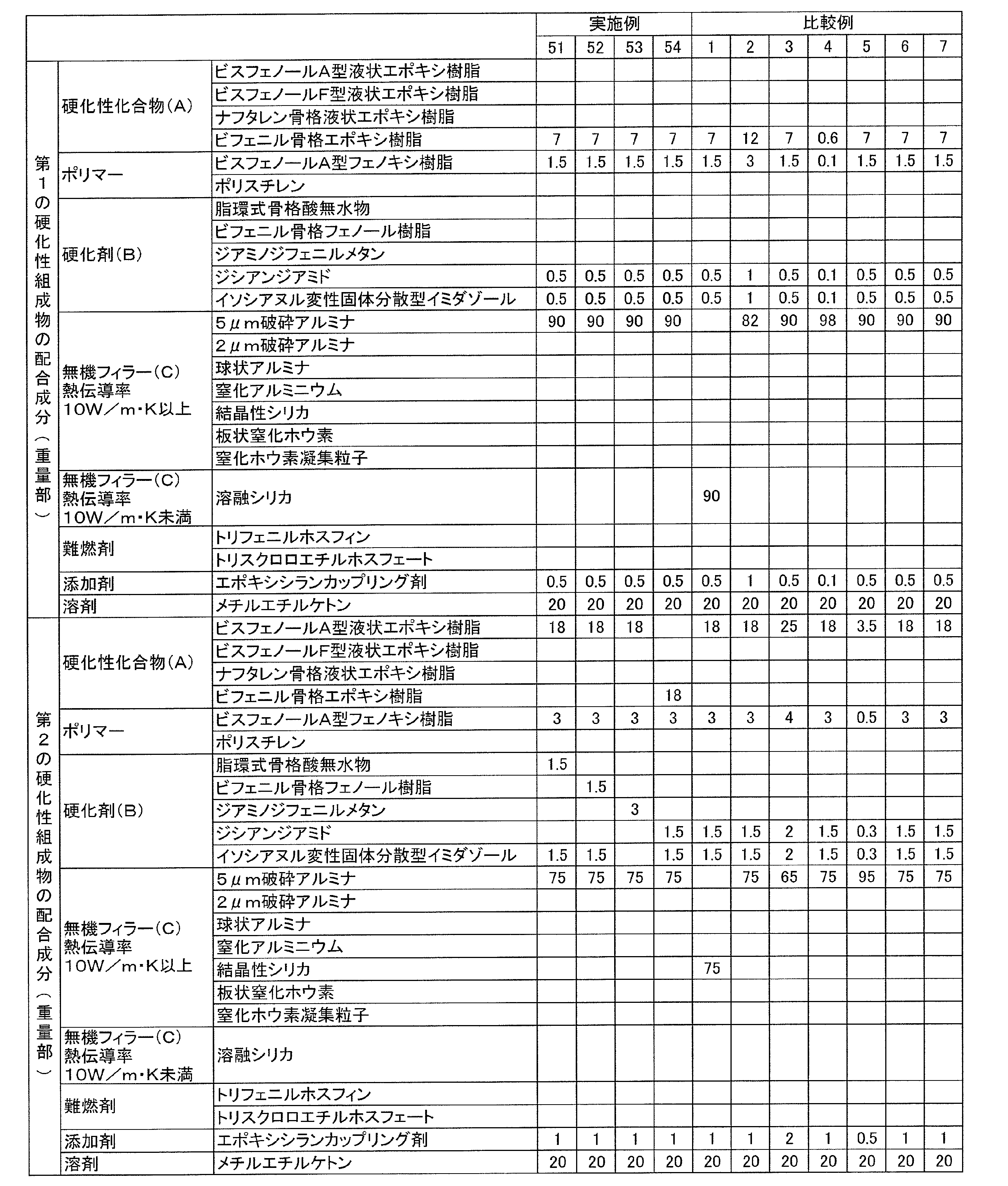


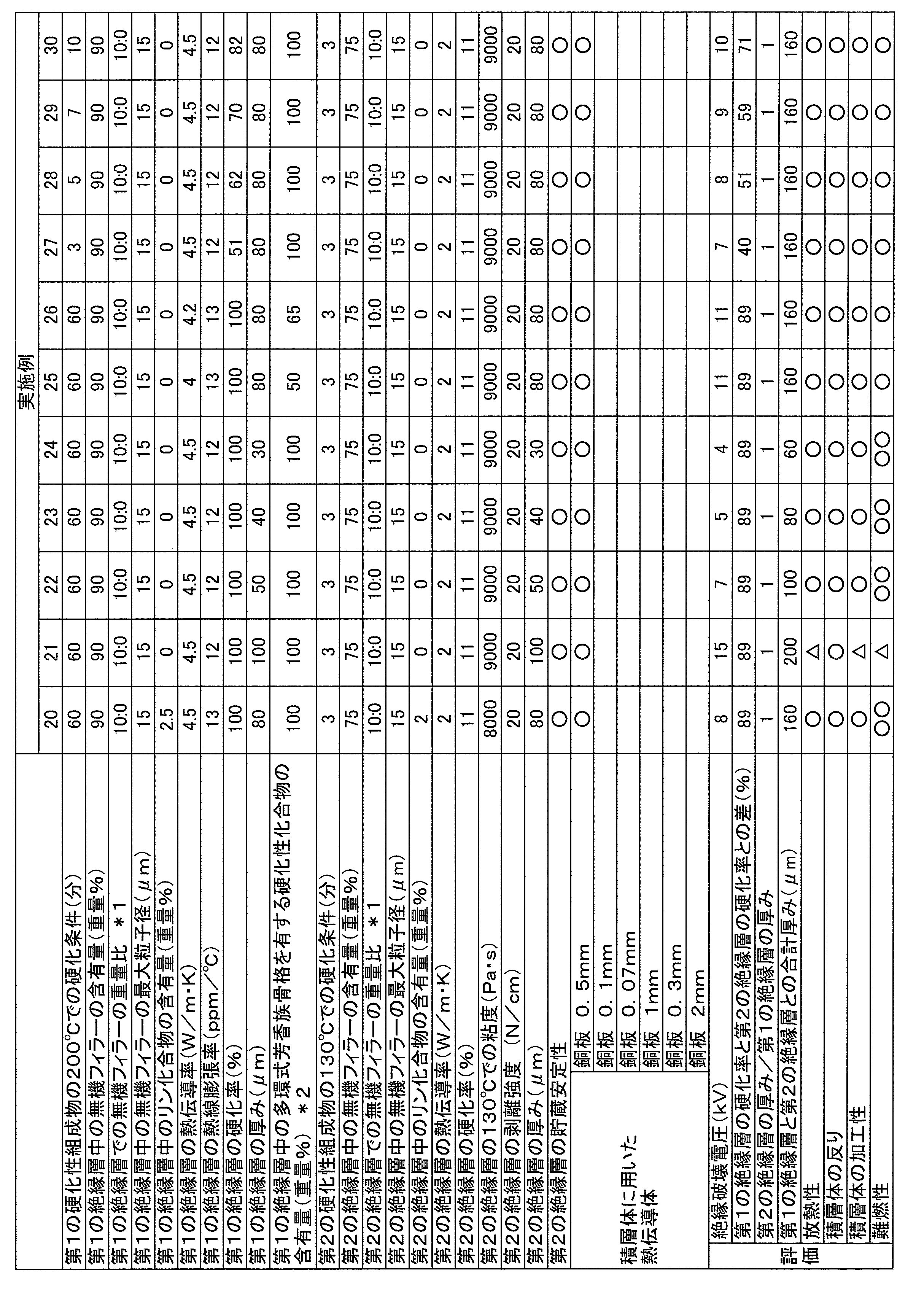
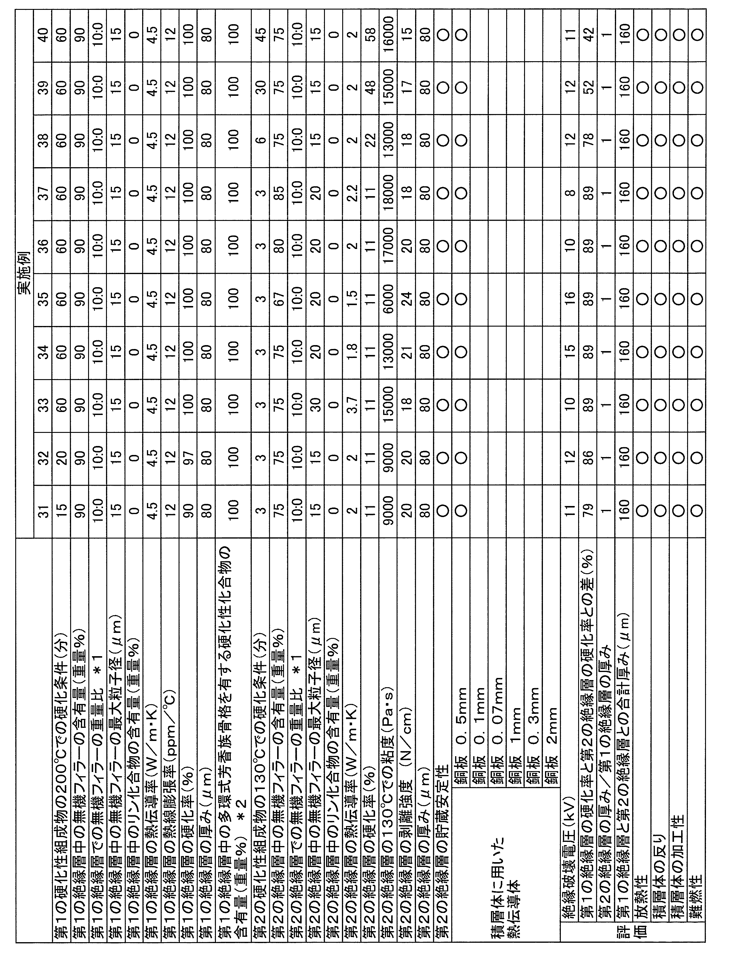
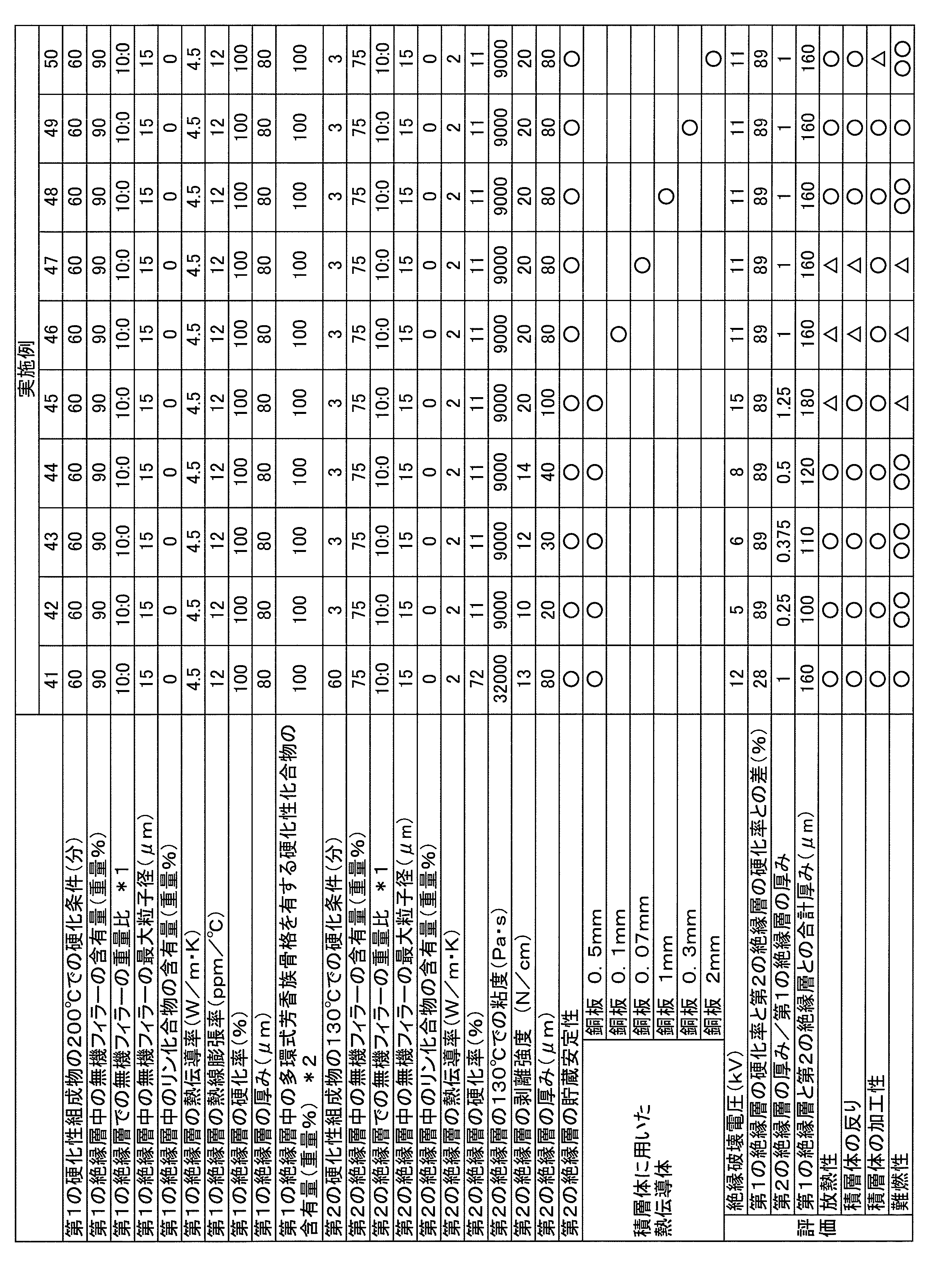
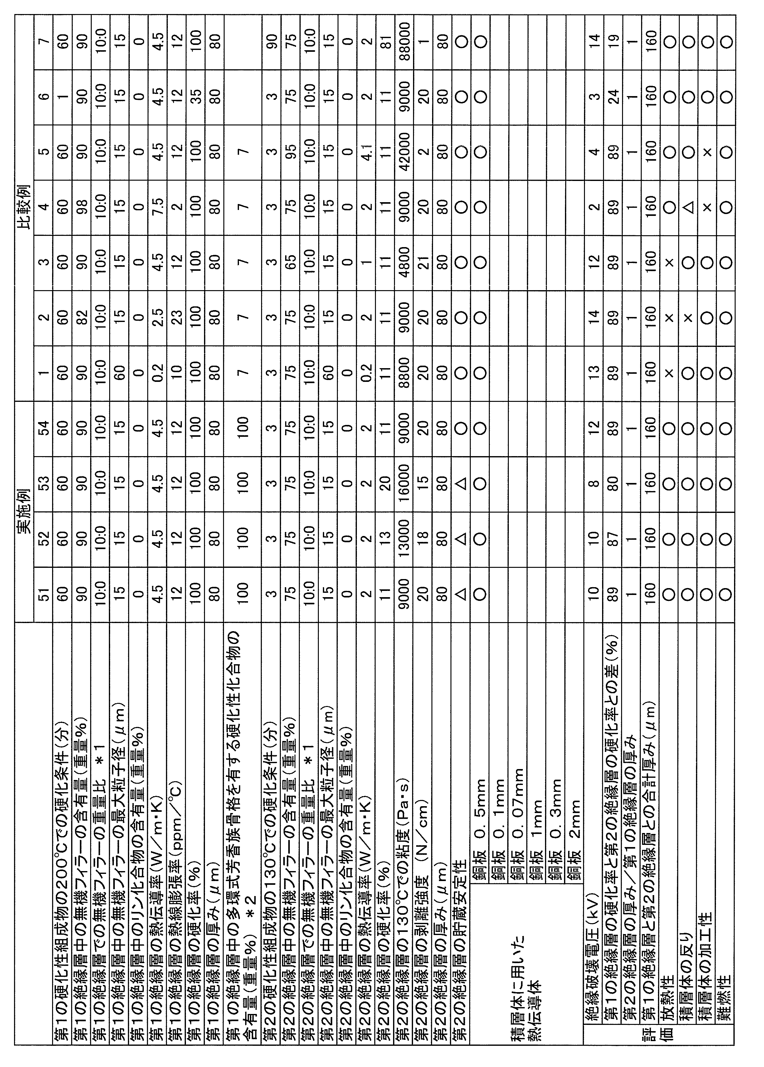
2…熱伝導体
3…第1の絶縁層
4…第2の絶縁層
11…パワー半導体モジュール用部品
12…導電層
13…モールド樹脂
Claims (19)
- 熱伝導率が10W/m・K以上である熱伝導体と、
前記熱伝導体の表面に積層されており、かつ半硬化物又は硬化物である第1の絶縁層と、
前記第1の絶縁層の前記熱伝導体側とは反対の表面に積層されており、かつ未硬化物又は半硬化物である第2の絶縁層とを備え、
前記第1の絶縁層が、熱伝導率が10W/m・K以上である無機フィラーを86重量%以上、97重量%未満で含み、かつ前記第2の絶縁層が、無機フィラーを67重量%以上、95重量%未満で含み、
前記第1の絶縁層の硬化率が50%以上であり、前記第2の絶縁層の硬化率が80%未満であり、かつ前記第1の絶縁層の硬化率が前記第2の絶縁層の硬化率よりも大きい、積層体。 - 前記第1の絶縁層100重量%中の前記無機フィラーの含有量が、前記第2の層100重量%中の前記無機フィラーの含有量よりも多い、請求項1に記載の積層体。
- パワー半導体モジュール用部品を得るために用いられる積層体である、請求項1又は2に記載の積層体。
- 前記第1の絶縁層100重量%中の前記無機フィラーの含有量が、前記第2の層100重量%中の前記無機フィラーの含有量よりも多く、
パワー半導体モジュール用部品を得るために用いられる積層体である、請求項1に記載の積層体。 - 前記第1の絶縁層が硬化物である場合に硬化物である前記第1の絶縁層の熱線膨張率が20ppm/℃以下であり、
前記第1の絶縁層が半硬化物である場合に硬化後の硬化物である前記第1の絶縁層の熱線膨張率が20ppm/℃以下である、請求項1~4のいずれか1項に記載の積層体。 - 前記第2の絶縁層の130℃での粘度が1000Pa・s以上、20000Pa・s以下である、請求項1~5のいずれか1項に記載の積層体。
- 前記第2の絶縁層の厚みの前記第1の絶縁層の厚みに対する比が、0.3以上、1以下である、請求項1~6のいずれか1項に記載の積層体。
- 前記第1の絶縁層に含まれている前記無機フィラーの最大粒子径が50μm以下であり、かつ前記第2の絶縁層に含まれている前記無機フィラーの最大粒子径が50μm以下である、請求項1~7のいずれか1項に記載の積層体。
- 前記第1の絶縁層に含まれている前記無機フィラーが、アルミナ、結晶性シリカ、窒化ホウ素及び窒化アルミニウムからなる群から選択された少なくとも1種である、請求項1~8のいずれか1項に記載の積層体。
- 前記第1の絶縁層に含まれている前記無機フィラー、及び、前記第2の絶縁層に含まれている前記無機フィラーがそれぞれ、アルミナ、結晶性シリカ、窒化ホウ素及び窒化アルミニウムからなる群から選択された少なくとも1種である、請求項1~9のいずれか1項に記載の積層体。
- 前記第1の絶縁層に含まれている前記無機フィラーが、アルミナ、結晶性シリカ及び窒化ホウ素からなる群から選択された少なくとも1種である、請求項1~10のいずれか1項に記載の積層体。
- 前記第1の絶縁層が、環状エーテル基を有する硬化性化合物と硬化剤とを用いて形成されている、請求項1~11のいずれか1項に記載の積層体。
- 前記第1の絶縁層に用いられている硬化剤が、融点が180℃以上であるアミン硬化剤である、請求項12に記載の積層体。
- 前記第1の絶縁層に用いられている前記環状エーテル基を有する硬化性化合物が、環状エーテル基及び多環式芳香族骨格を有する硬化性化合物を含む、請求項12又は13に記載の積層体。
- 前記多環式芳香族骨格がビフェニル骨格である、請求項14に記載の積層体。
- 前記第2の絶縁層が、環状エーテル基を有する硬化性化合物と硬化剤とを用いて形成されている、請求項1~15のいずれか1項に記載の積層体。
- 前記第2の絶縁層に用いられている硬化剤が、融点が180℃以上であるアミン硬化剤である、請求項16に記載の積層体。
- 前記熱伝導体の厚みが100μm以上、1mm以下である、請求項1~17のいずれか1項に記載の積層体。
- 請求項1~18のいずれか1項に記載の積層体を用いて、
前記積層体における前記第2の絶縁層の前記第1の絶縁層側とは反対の表面に導電層を積層する工程と、
前記第2の絶縁層を硬化させ、かつ前記第1の絶縁層が半硬化物である場合に前記第1の絶縁層を硬化させる工程と、
前記熱伝導体と前記第1の絶縁層と前記第2の絶縁層と前記導電層とをモールド樹脂内に埋め込む工程とを備える、パワー半導体モジュール用部品の製造方法。
Priority Applications (2)
| Application Number | Priority Date | Filing Date | Title |
|---|---|---|---|
| CN201280040555.8A CN103748673B (zh) | 2011-10-28 | 2012-10-24 | 叠层体及功率半导体模块用部件的制造方法 |
| KR1020137029905A KR101612596B1 (ko) | 2011-10-28 | 2012-10-24 | 적층체 및 파워 반도체 모듈용 부품의 제조 방법 |
Applications Claiming Priority (2)
| Application Number | Priority Date | Filing Date | Title |
|---|---|---|---|
| JP2011-237076 | 2011-10-28 | ||
| JP2011237076 | 2011-10-28 |
Publications (1)
| Publication Number | Publication Date |
|---|---|
| WO2013061981A1 true WO2013061981A1 (ja) | 2013-05-02 |
Family
ID=48167808
Family Applications (1)
| Application Number | Title | Priority Date | Filing Date |
|---|---|---|---|
| PCT/JP2012/077406 Ceased WO2013061981A1 (ja) | 2011-10-28 | 2012-10-24 | 積層体及びパワー半導体モジュール用部品の製造方法 |
Country Status (4)
| Country | Link |
|---|---|
| KR (1) | KR101612596B1 (ja) |
| CN (1) | CN103748673B (ja) |
| TW (1) | TWI543312B (ja) |
| WO (1) | WO2013061981A1 (ja) |
Cited By (1)
| Publication number | Priority date | Publication date | Assignee | Title |
|---|---|---|---|---|
| JP2021150638A (ja) * | 2020-03-13 | 2021-09-27 | 大日本印刷株式会社 | リードフレーム、リードフレームの製造方法及び半導体装置の製造方法 |
Families Citing this family (8)
| Publication number | Priority date | Publication date | Assignee | Title |
|---|---|---|---|---|
| WO2017057553A1 (ja) * | 2015-09-30 | 2017-04-06 | 積水化学工業株式会社 | 積層体 |
| TWI622139B (zh) * | 2016-03-08 | 2018-04-21 | 恆勁科技股份有限公司 | 封裝基板 |
| WO2018235919A1 (ja) * | 2017-06-23 | 2018-12-27 | 積水化学工業株式会社 | 放熱シート、放熱シートの製造方法及び積層体 |
| US11548264B2 (en) | 2018-04-17 | 2023-01-10 | Sekisui Chemical Co., Ltd. | Insulation sheet, laminate, and substrate |
| CN108610629A (zh) * | 2018-04-27 | 2018-10-02 | 川叶电子科技(上海)股份有限公司 | 一种改性增强耐电晕电线及其制备方法 |
| KR102849602B1 (ko) * | 2019-09-30 | 2025-08-21 | 가부시키가이샤 플로스피아 | 적층 구조체 및 반도체 장치 |
| CN111508902B (zh) * | 2020-04-26 | 2021-09-10 | 全球能源互联网研究院有限公司 | 一种绝缘结构、包覆芯片周缘的绝缘件及其制备方法 |
| JP7248867B2 (ja) * | 2020-05-15 | 2023-03-29 | デンカ株式会社 | 複合体シート及び積層体 |
Citations (6)
| Publication number | Priority date | Publication date | Assignee | Title |
|---|---|---|---|---|
| JPS607195A (ja) * | 1983-06-24 | 1985-01-14 | 松下電器産業株式会社 | 高熱伝導性金属ベ−スプリント基板の製造方法 |
| JPH08332696A (ja) * | 1995-06-06 | 1996-12-17 | Hitachi Chem Co Ltd | 絶縁接着材料付き金属体及びその製造方法 |
| JP2001203313A (ja) * | 1999-11-09 | 2001-07-27 | Matsushita Electric Ind Co Ltd | 熱伝導基板およびその製造方法 |
| JP2009227947A (ja) * | 2008-03-25 | 2009-10-08 | Mitsubishi Electric Corp | 熱伝導性樹脂組成物、熱伝導性樹脂シート及びパワーモジュール |
| JP2011070930A (ja) * | 2009-09-25 | 2011-04-07 | Sekisui Chem Co Ltd | 多層絶縁シート及び積層構造体 |
| JP2011176024A (ja) * | 2010-02-23 | 2011-09-08 | Mitsubishi Electric Corp | 熱硬化性樹脂組成物、bステージ熱伝導性シート及びパワーモジュール |
Family Cites Families (3)
| Publication number | Priority date | Publication date | Assignee | Title |
|---|---|---|---|---|
| US6570099B1 (en) * | 1999-11-09 | 2003-05-27 | Matsushita Electric Industrial Co., Ltd. | Thermal conductive substrate and the method for manufacturing the same |
| US6919504B2 (en) * | 2002-12-19 | 2005-07-19 | 3M Innovative Properties Company | Flexible heat sink |
| JP2005109100A (ja) * | 2003-09-30 | 2005-04-21 | Mitsubishi Electric Corp | 半導体装置およびその製造方法 |
-
2012
- 2012-10-24 CN CN201280040555.8A patent/CN103748673B/zh active Active
- 2012-10-24 KR KR1020137029905A patent/KR101612596B1/ko active Active
- 2012-10-24 WO PCT/JP2012/077406 patent/WO2013061981A1/ja not_active Ceased
- 2012-10-26 TW TW101139807A patent/TWI543312B/zh not_active IP Right Cessation
Patent Citations (6)
| Publication number | Priority date | Publication date | Assignee | Title |
|---|---|---|---|---|
| JPS607195A (ja) * | 1983-06-24 | 1985-01-14 | 松下電器産業株式会社 | 高熱伝導性金属ベ−スプリント基板の製造方法 |
| JPH08332696A (ja) * | 1995-06-06 | 1996-12-17 | Hitachi Chem Co Ltd | 絶縁接着材料付き金属体及びその製造方法 |
| JP2001203313A (ja) * | 1999-11-09 | 2001-07-27 | Matsushita Electric Ind Co Ltd | 熱伝導基板およびその製造方法 |
| JP2009227947A (ja) * | 2008-03-25 | 2009-10-08 | Mitsubishi Electric Corp | 熱伝導性樹脂組成物、熱伝導性樹脂シート及びパワーモジュール |
| JP2011070930A (ja) * | 2009-09-25 | 2011-04-07 | Sekisui Chem Co Ltd | 多層絶縁シート及び積層構造体 |
| JP2011176024A (ja) * | 2010-02-23 | 2011-09-08 | Mitsubishi Electric Corp | 熱硬化性樹脂組成物、bステージ熱伝導性シート及びパワーモジュール |
Cited By (2)
| Publication number | Priority date | Publication date | Assignee | Title |
|---|---|---|---|---|
| JP2021150638A (ja) * | 2020-03-13 | 2021-09-27 | 大日本印刷株式会社 | リードフレーム、リードフレームの製造方法及び半導体装置の製造方法 |
| JP7620867B2 (ja) | 2020-03-13 | 2025-01-24 | 大日本印刷株式会社 | リードフレーム、リードフレームの製造方法及び半導体装置の製造方法 |
Also Published As
| Publication number | Publication date |
|---|---|
| CN103748673A (zh) | 2014-04-23 |
| KR101612596B1 (ko) | 2016-04-14 |
| TW201320260A (zh) | 2013-05-16 |
| CN103748673B (zh) | 2016-12-14 |
| TWI543312B (zh) | 2016-07-21 |
| KR20140088047A (ko) | 2014-07-09 |
Similar Documents
| Publication | Publication Date | Title |
|---|---|---|
| KR101174971B1 (ko) | 절연 시트 및 적층 구조체 | |
| CN103748673B (zh) | 叠层体及功率半导体模块用部件的制造方法 | |
| JP4495772B1 (ja) | 絶縁シート及び積層構造体 | |
| JP4922220B2 (ja) | 絶縁シート及び積層構造体 | |
| JP2009144072A (ja) | 絶縁シート及び積層構造体 | |
| WO2010016480A1 (ja) | 絶縁シート及び積層構造体 | |
| JP2011070930A (ja) | 多層絶縁シート及び積層構造体 | |
| JP2011168672A (ja) | 絶縁シート | |
| JP2013098217A (ja) | パワー半導体モジュール用部品の製造方法 | |
| WO2012073360A1 (ja) | 絶縁シート及び積層構造体 | |
| JP6235733B2 (ja) | 積層体 | |
| JP4987161B1 (ja) | 絶縁材料 | |
| JP5346363B2 (ja) | 積層体 | |
| JP5092050B1 (ja) | 積層体 | |
| JP2013206902A (ja) | パワー半導体モジュール用部品の製造方法 | |
| JP2017217882A (ja) | 積層体、接着層及び金属材付き半導体チップ、及び半導体装置の製造方法 | |
| JP2011124078A (ja) | 絶縁シート、積層構造体及び積層構造体の製造方法 | |
| JP2009224110A (ja) | 絶縁シート及び積層構造体 | |
| JP2013201338A (ja) | パワー半導体モジュール用部品の製造方法 | |
| JP5114597B1 (ja) | 積層体及び切断積層体 | |
| JP5837839B2 (ja) | 積層構造体 | |
| JP2013107353A (ja) | 積層構造体 | |
| JP2012229319A (ja) | 絶縁材料及び積層構造体 | |
| JP2017186483A (ja) | 積層シート、接着層及び金属材付き半導体チップの製造方法、及び半導体装置の製造方法 | |
| JP5276193B1 (ja) | 積層体の製造方法 |
Legal Events
| Date | Code | Title | Description |
|---|---|---|---|
| 121 | Ep: the epo has been informed by wipo that ep was designated in this application |
Ref document number: 12842795 Country of ref document: EP Kind code of ref document: A1 |
|
| ENP | Entry into the national phase |
Ref document number: 20137029905 Country of ref document: KR Kind code of ref document: A |
|
| NENP | Non-entry into the national phase |
Ref country code: DE |
|
| 122 | Ep: pct application non-entry in european phase |
Ref document number: 12842795 Country of ref document: EP Kind code of ref document: A1 |
|
| NENP | Non-entry into the national phase |
Ref country code: JP |