WO2013046292A1 - Module émetteur de lumière et appareil d'éclairage - Google Patents
Module émetteur de lumière et appareil d'éclairage Download PDFInfo
- Publication number
- WO2013046292A1 WO2013046292A1 PCT/JP2011/071865 JP2011071865W WO2013046292A1 WO 2013046292 A1 WO2013046292 A1 WO 2013046292A1 JP 2011071865 W JP2011071865 W JP 2011071865W WO 2013046292 A1 WO2013046292 A1 WO 2013046292A1
- Authority
- WO
- WIPO (PCT)
- Prior art keywords
- light emitting
- emitting module
- light
- sealing member
- substrate
- Prior art date
Links
- 239000000758 substrate Substances 0.000 claims abstract description 68
- 239000004065 semiconductor Substances 0.000 claims abstract description 16
- 238000007789 sealing Methods 0.000 claims description 56
- 230000000630 rising effect Effects 0.000 claims description 2
- 238000000605 extraction Methods 0.000 description 19
- 229910052802 copper Inorganic materials 0.000 description 10
- 239000010949 copper Substances 0.000 description 10
- RYGMFSIKBFXOCR-UHFFFAOYSA-N Copper Chemical compound [Cu] RYGMFSIKBFXOCR-UHFFFAOYSA-N 0.000 description 9
- 239000000919 ceramic Substances 0.000 description 8
- OAICVXFJPJFONN-UHFFFAOYSA-N Phosphorus Chemical compound [P] OAICVXFJPJFONN-UHFFFAOYSA-N 0.000 description 7
- 230000004907 flux Effects 0.000 description 7
- 239000000463 material Substances 0.000 description 7
- 229910052751 metal Inorganic materials 0.000 description 6
- 239000002184 metal Substances 0.000 description 6
- 229910052782 aluminium Inorganic materials 0.000 description 5
- XAGFODPZIPBFFR-UHFFFAOYSA-N aluminium Chemical compound [Al] XAGFODPZIPBFFR-UHFFFAOYSA-N 0.000 description 5
- PXHVJJICTQNCMI-UHFFFAOYSA-N Nickel Chemical compound [Ni] PXHVJJICTQNCMI-UHFFFAOYSA-N 0.000 description 4
- 230000002596 correlated effect Effects 0.000 description 4
- 238000009434 installation Methods 0.000 description 4
- BQCADISMDOOEFD-UHFFFAOYSA-N Silver Chemical compound [Ag] BQCADISMDOOEFD-UHFFFAOYSA-N 0.000 description 3
- 238000005219 brazing Methods 0.000 description 3
- 230000007423 decrease Effects 0.000 description 3
- PCHJSUWPFVWCPO-UHFFFAOYSA-N gold Chemical compound [Au] PCHJSUWPFVWCPO-UHFFFAOYSA-N 0.000 description 3
- 229910052737 gold Inorganic materials 0.000 description 3
- 239000010931 gold Substances 0.000 description 3
- 230000004048 modification Effects 0.000 description 3
- 238000012986 modification Methods 0.000 description 3
- 229910052709 silver Inorganic materials 0.000 description 3
- 239000004332 silver Substances 0.000 description 3
- 230000017525 heat dissipation Effects 0.000 description 2
- 238000005286 illumination Methods 0.000 description 2
- 229910052759 nickel Inorganic materials 0.000 description 2
- 238000007747 plating Methods 0.000 description 2
- 229920001707 polybutylene terephthalate Polymers 0.000 description 2
- 229920005989 resin Polymers 0.000 description 2
- 239000011347 resin Substances 0.000 description 2
- 229910018072 Al 2 O 3 Inorganic materials 0.000 description 1
- 239000004593 Epoxy Substances 0.000 description 1
- 238000006243 chemical reaction Methods 0.000 description 1
- 230000000295 complement effect Effects 0.000 description 1
- 230000003247 decreasing effect Effects 0.000 description 1
- 230000006866 deterioration Effects 0.000 description 1
- 238000004512 die casting Methods 0.000 description 1
- 230000000694 effects Effects 0.000 description 1
- 238000010292 electrical insulation Methods 0.000 description 1
- 238000005530 etching Methods 0.000 description 1
- 230000005496 eutectics Effects 0.000 description 1
- 239000011521 glass Substances 0.000 description 1
- 238000001746 injection moulding Methods 0.000 description 1
- 238000004519 manufacturing process Methods 0.000 description 1
- 239000000203 mixture Substances 0.000 description 1
- 239000002245 particle Substances 0.000 description 1
- 238000000059 patterning Methods 0.000 description 1
- 230000002093 peripheral effect Effects 0.000 description 1
- -1 polybutylene terephthalate Polymers 0.000 description 1
- 230000009103 reabsorption Effects 0.000 description 1
- 229910000679 solder Inorganic materials 0.000 description 1
- 229920003002 synthetic resin Polymers 0.000 description 1
- 239000000057 synthetic resin Substances 0.000 description 1
Images


Classifications
-
- F—MECHANICAL ENGINEERING; LIGHTING; HEATING; WEAPONS; BLASTING
- F21—LIGHTING
- F21S—NON-PORTABLE LIGHTING DEVICES; SYSTEMS THEREOF; VEHICLE LIGHTING DEVICES SPECIALLY ADAPTED FOR VEHICLE EXTERIORS
- F21S8/00—Lighting devices intended for fixed installation
- F21S8/02—Lighting devices intended for fixed installation of recess-mounted type, e.g. downlighters
- F21S8/026—Lighting devices intended for fixed installation of recess-mounted type, e.g. downlighters intended to be recessed in a ceiling or like overhead structure, e.g. suspended ceiling
-
- F—MECHANICAL ENGINEERING; LIGHTING; HEATING; WEAPONS; BLASTING
- F21—LIGHTING
- F21V—FUNCTIONAL FEATURES OR DETAILS OF LIGHTING DEVICES OR SYSTEMS THEREOF; STRUCTURAL COMBINATIONS OF LIGHTING DEVICES WITH OTHER ARTICLES, NOT OTHERWISE PROVIDED FOR
- F21V29/00—Protecting lighting devices from thermal damage; Cooling or heating arrangements specially adapted for lighting devices or systems
- F21V29/85—Protecting lighting devices from thermal damage; Cooling or heating arrangements specially adapted for lighting devices or systems characterised by the material
-
- F—MECHANICAL ENGINEERING; LIGHTING; HEATING; WEAPONS; BLASTING
- F21—LIGHTING
- F21Y—INDEXING SCHEME ASSOCIATED WITH SUBCLASSES F21K, F21L, F21S and F21V, RELATING TO THE FORM OR THE KIND OF THE LIGHT SOURCES OR OF THE COLOUR OF THE LIGHT EMITTED
- F21Y2105/00—Planar light sources
- F21Y2105/10—Planar light sources comprising a two-dimensional array of point-like light-generating elements
-
- F—MECHANICAL ENGINEERING; LIGHTING; HEATING; WEAPONS; BLASTING
- F21—LIGHTING
- F21Y—INDEXING SCHEME ASSOCIATED WITH SUBCLASSES F21K, F21L, F21S and F21V, RELATING TO THE FORM OR THE KIND OF THE LIGHT SOURCES OR OF THE COLOUR OF THE LIGHT EMITTED
- F21Y2115/00—Light-generating elements of semiconductor light sources
- F21Y2115/10—Light-emitting diodes [LED]
-
- H—ELECTRICITY
- H01—ELECTRIC ELEMENTS
- H01L—SEMICONDUCTOR DEVICES NOT COVERED BY CLASS H10
- H01L2924/00—Indexing scheme for arrangements or methods for connecting or disconnecting semiconductor or solid-state bodies as covered by H01L24/00
- H01L2924/0001—Technical content checked by a classifier
- H01L2924/0002—Not covered by any one of groups H01L24/00, H01L24/00 and H01L2224/00
-
- H—ELECTRICITY
- H01—ELECTRIC ELEMENTS
- H01L—SEMICONDUCTOR DEVICES NOT COVERED BY CLASS H10
- H01L33/00—Semiconductor devices having potential barriers specially adapted for light emission; Processes or apparatus specially adapted for the manufacture or treatment thereof or of parts thereof; Details thereof
- H01L33/48—Semiconductor devices having potential barriers specially adapted for light emission; Processes or apparatus specially adapted for the manufacture or treatment thereof or of parts thereof; Details thereof characterised by the semiconductor body packages
- H01L33/52—Encapsulations
- H01L33/54—Encapsulations having a particular shape
Definitions
- Embodiments of the present invention relate to a light emitting module in which a semiconductor light emitting element such as an LED (light emitting diode) is mounted on a substrate, and a lighting fixture incorporating the light emitting module.
- a semiconductor light emitting element such as an LED (light emitting diode) is mounted on a substrate
- a lighting fixture incorporating the light emitting module.
- a lens type in which a plurality of LEDs arranged side by side on a substrate are individually sealed with a sealing member, a line type in which a plurality of LEDs are arranged in a row and sealed, or a frame surrounding a plurality of LEDs A bank type in which a (bank) is provided and a plurality of LEDs are sealed together is generally known.
- the sealing member that seals the LED to the substrate is a translucent material including phosphor particles that excite and emit light having a complementary color relationship with the emission color of the LED, and light emitted directly from the LED. Mix to emit white light.
- a sealing member that includes a phosphor that is excited by blue light and emits yellow light or red light is sealed with a sealing member that includes a phosphor that is excited by blue light and emits yellow light or red light.
- the light-emitting module includes a plurality of semiconductor light-emitting elements mounted on the substrate surface, and a sealing member that seals the semiconductor light-emitting elements on the substrate surface at intervals.
- the surface of the sealing member that individually seals the semiconductor light emitting element includes a side surface that rises linearly in a direction away from the substrate surface, and a top surface that is continuous with the side surface on the side away from the substrate surface.
- the light extraction efficiency can be increased.
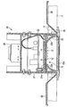
- FIG. 1 is a sectional view of the lighting fixture concerning an embodiment.
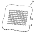
- FIG. 2 is a front view of the lighting apparatus of FIG. 1 as viewed from the light extraction side.
- FIG. 3 is a perspective view of the light emitting module according to the embodiment as viewed from the light extraction side. 4 is a partially enlarged cross-sectional view of the light emitting module of FIG.
- FIG. 5 is a cross-sectional view showing a mounted state of the LED chip incorporated in the light emitting module of FIG.
- FIG. 6 is a cross-sectional view showing a modification of the sealing member in which the LED chip of the light emitting module of FIG. 3 is sealed.
- FIG. 7 is a cross-sectional view showing another modification of the sealing member in which the LED chip of the light emitting module of FIG.
- FIG. 8 is a perspective view of a conventional bank type light emitting module as seen from the light extraction side.
- FIG. 9 is a partially enlarged cross-sectional view of the light emitting module of FIG.
- FIG. 10 is a perspective view of a conventional line type light emitting module as seen from the light extraction side.
- FIG. 11 is a perspective view of a conventional lens-type light emitting module as seen from the light extraction side.
- 12 is a partially enlarged cross-sectional view of the light emitting module of FIGS.
- Drawing 1 is a sectional view of lighting fixture 20 concerning an embodiment.
- FIG. 2 is the front view which looked at this lighting fixture 20 from the light extraction side.
- the lighting fixture 20 is a downlight using a light emitting module 10 described later as a light source, and includes a case 21 to which the light emitting module 10 is attached and a lighting device 22 that lights the light emitting module 10.
- the case 21 is made of, for example, aluminum die casting and has a cylindrical shape having openings at both ends, and integrally includes a mounting plate 21a for mounting the light emitting module 10 therein.
- the light emitting module 10 is attached to the case 21 by fastening the substrate 11 to the attachment plate 21a with screws. At this time, the copper metal member 14 provided on the back surface of the substrate 11 is in close contact with the flat surface of the aluminum mounting plate 21a. As a result, heat generated from each light emitting unit 13 (to be described later) of the light emitting module 10 is efficiently radiated to the mounting plate 21 a through the substrate 11 and the metal member 14.
- the reflector 23 is attached to the inside of the case 21 on the surface side of the light emitting module 10.
- the reflector 23 is made of a white synthetic resin having light resistance, heat resistance and electrical insulation, for example, polybutylene terephthalate (PBT).
- PBT polybutylene terephthalate
- the reflector 23 has a circular opening 23a that surrounds the plurality of light emitting portions 13, and a so-called “mortar-shaped” reflecting surface 23b that expands from the edge of the opening 23a.
- the lighting device 22 includes a lighting circuit and a power supply circuit for lighting the plurality of light emitting units 13 of the light emitting module 10.
- the lighting device 22 converts an AC voltage of 100 V obtained from a commercial power source into a DC voltage of 24 V, and supplies a constant DC current to each light emitting unit 13.
- the lighting device 22 is housed inside the case 21.
- a power terminal block 24 for supplying power from the commercial power source to the lighting device 22 is provided at the end of the case 21 on the side opposite to the light extraction side.
- a decorative frame 25 is attached to the end of the case 21 on the light extraction side.
- the decorative frame 25 is adjacent to the light emitting area where the plurality of light emitting units 13 are arranged, and is covered with a transparent cover member 25a.
- a support 26 for holding the case 21 on the ceiling X is attached to the end of the case 21 on the light extraction side.
- the support 26 is a leaf spring.
- the power line wired in the installation hole H formed in the ceiling X is connected to the power terminal block 24.
- the support tool 26 is bent inward by hand, and the tip is inserted into the installation hole H together with the case 21, and then the hand is released from the support tool 26.
- the support 26 is restored by its own elasticity and pressed against the inner surface of the installation hole H, and the decorative frame 25 is brought into contact with the ceiling X so as to sandwich the ceiling X between the support 26 and the support X.
- the edge of the installation hole H is covered with the decorative frame 25.
- each light emitting unit 13 When the lighting fixture 20 having the above structure is turned on, most of the light emitted from each light emitting unit 13 is reflected directly or by the reflection surface 23b of the reflector 23 and spreads downward and radiated. At this time, part of the light emitted from the light emitting unit 13 is also reflected on the wiring pattern on the substrate surface and the substrate surface.
- the surface of the wiring pattern is plated with nickel, silver, gold or the like.
- the substrate 11 is made of white ceramics. For this reason, the light is well reflected on the surface of the wiring pattern and the surface of the substrate 11 so that the entire lighting fixture 20 can maintain a desired light emission amount.
- the LED chip 2 of each light emitting unit 13 when the lighting fixture 20 is turned on as described above, the LED chip 2 of each light emitting unit 13 generates heat. In order to prevent deterioration over time due to heat of the light emitting unit 13, it is necessary to efficiently dissipate this heat.
- the metal member 14 attached to the back side of the substrate 11 is made of copper having excellent thermal conductivity
- the substrate 11 itself is made of ceramics having good thermal conductivity
- the case 21 is also made of Since it is formed of aluminum having excellent thermal conductivity, the heat generated from the light emitting portion 13 is transmitted from the wiring pattern 12 to the metal member 14 through the insulating substrate 11, and further, the heat transfer surface of the mounting plate 21a. Is transmitted to the case 21 via.
- the heat transmitted to the case 21 is radiated to the outside of the lighting fixture 20. That is, the heat from each light emitting part 13 is effectively radiated to the outside from the side wall of the case 21 having a large surface area.
- the lighting fixture 20 of this embodiment suppresses a decrease in the light conversion efficiency of each light-emitting unit 13 by the above-described heat dissipation action, and performs illumination with bright illuminance. Moreover, the lifetime of the light emission part 13 is also extended by the above-mentioned heat dissipation action.
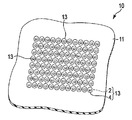
- FIG. 3 is a perspective view of the light emitting module 10 of this embodiment incorporated in the lighting fixture 20 as seen from the light extraction side.
- FIG. 4 is a partially enlarged cross-sectional view of the light emitting module 10 of FIG. 1 and 2, the light emitting module 10 having 25 light emitting units 13 has been described. However, the number of the light emitting units 13 may be any number, and at least one may be used. Here, 96 light emitting units 13 are provided. The light emitting module 10 having the above will be described.
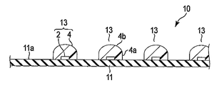
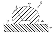
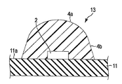
- the light emitting module 10 includes a substrate 11 having a wiring pattern (not shown) on the surface, a plurality of LED chips 2 (semiconductor light emitting elements) mounted on the surface 11a of the substrate 11 and electrically connected to the wiring pattern, And it has the some sealing member 4 which seals each LED chip 2 on the surface 11a of the board
- Each LED chip 2 and the sealing member 4 that seals it constitute the light emitting unit 13 described above.
- the substrate 11 is a DCB (Direct Copper Bonding) substrate, DBA (Direct Brazing Aluminum) substrate, AMC (Active Metal Brazed Copper) substrate, DPC (Direct Plated Copper) substrate, metal substrate, ceramic substrate, glass epoxy substrate, or the like.
- the DCB substrate is formed by directly bonding a copper plate to a ceramic base material.
- the DBA substrate is formed by brazing an aluminum plate on a ceramic base material.
- the AMC substrate is formed by brazing a copper plate on a ceramic base material.
- the DPC board is a ceramic base material plated with copper. Incidentally, it is possible to use as a ceramic substrate, Al 2 O 3, AlN, etc. Si 3 N 4.
- a wiring pattern (not shown) is provided on the surface 11 a of the substrate 11.
- the wiring pattern is formed by etching copper provided on the substrate surface 11a and patterning the gold pattern or silver plating on the copper pattern via nickel plating.
- the LED chip 2 of this embodiment is of a type that is flip-chip connected to the substrate surface 11a, and the light emitting layer 2a is close to the substrate surface 11a.
- Each LED chip 2 has a bump 2b for connecting to the wiring pattern.
- the LED chip 2 is connected to the wiring pattern on the substrate surface 11a by eutectic solder 3, for example.
- silver paste or gold bumps may be used.
- the LED chip 2 of the present embodiment is a blue light emitting diode that emits blue light when energized.
- the sealing member 4 is a translucent resin containing a phosphor.
- the sealing member 4 including a phosphor that is excited by blue light and emits yellow light and red light is used.
- the sealing member 4 is provided on the substrate surface 11 a so as to cover the entire surface of the LED chip 2.
- the shape of the sealing member 4 is designed such that the surface thereof includes a side surface 4a that rises linearly in a direction away from the substrate surface 11a, and a top surface 4b that is continuous with the side surface 4a on the side away from the substrate surface 11a.
- This shape is a so-called bullet shape.
- the side surface 4a may be substantially perpendicular to the substrate surface 11a.
- the side surface 4a may be inclined slightly inward toward the substrate surface 11a (downward in the drawing).
- it may be slightly inclined outward toward the substrate surface 11a. That is, the expression “rising up in a straight line” described above includes those in FIGS. 6 and 7.
- the sealing member 4 is formed by resin injection molding, it is desirable to design the sealing member 4 so as to slightly widen the bottom of the sealing member 4 as shown in FIG.
- the top surface 4b is not limited to a spherical surface, and may be any shape as long as it can increase the light emission efficiency, such as a flat surface, a concave surface, or a concave and convex surface. You can choose. For example, when it is desired to reduce the luminous intensity of the central part and spread the light to the peripheral part, it is preferable to use a concave surface, and to increase the degree of color mixing of the light emitted from the sealing member 4, it is preferable to use an uneven surface.
- the shape of the top surface 4b is, for example, a spherical shape that is smoothly continuous with an end portion (upper end in the drawing) of the side surface 4a that is spaced from the substrate surface 11a. preferable.
- the LED chip 2 of the present embodiment has a flat rectangular block shape, is a square having a side length of 1 mm, and a mounting height from the substrate surface 11a is 0.17 mm.
- 96 LED chips 2 are arranged 8 ⁇ 12 vertically and horizontally on the substrate surface 11a. At this time, the pitch of each LED chip 2 was set to 3.0 mm in length and 2.5 mm in width.
- the sealing member 4 of the present embodiment has the above-mentioned bullet shape, its side surface 4a has a cylindrical shape with a diameter of 1.7 mm and a height of 0.41 mm, and its top surface 4b has a curvature radius of 1.1 mm. It is made spherical. In this case, the height of the sealing member 4 including the top surface 4b from the substrate surface 11a is about 1 mm.
- the sealing member 4 since the sealing member 4 has the side surface 4a that rises substantially perpendicularly from the substrate surface 11a, in addition to the light directly emitted through the side surface 4a, the light toward the substrate surface 11a and the side surface 4a A large amount of light that is effective for illumination in the light extraction direction, such as light that is reflected on the inside and emitted through the top surface 4b, can be extracted.
- the light extraction efficiency can be further increased. That is, at a pitch at which light emitted from one light emitting unit 13 through the sealing member 4 is not absorbed by the sealing member 4 of the adjacent light emitting unit 13 and does not cause luminance unevenness. It is desirable to design.
- each part of the light emitting part 13 it is desirable to mount the LED chip 2 on the substrate surface 11a as in the present embodiment.
- the face-up type LED chip is wire-bonded to the wiring pattern on the substrate surface, it is necessary to connect the bonding wire by arranging an electrode pad at the end of the chip on the light extraction side, resulting in a decrease in luminous efficiency. At the same time, the diameter of the sealing member is increased.
- the light emitted from the LED chip 2 may be absorbed before exiting the sealing member, and the light emission efficiency may be decreased accordingly.
- the pitch between the chips is not changed, the distance between the sealing member surfaces in the adjacent light emitting parts is shortened, and light is reabsorbed by the adjacent light emitting parts, and the luminous efficiency is accordingly increased. descend.
- the diameter of the sealing member is increased, the material cost is increased accordingly, and the module is also increased in size.
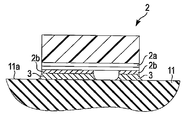
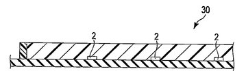
- the light emitting module 30 has a structure in which a bank 32 surrounding all the LED chips 2 arranged in the vertical and horizontal directions is provided, and a sealing member 34 is filled in the bank 32 to seal all the LED chips 2.
- Other structures have the same structure as the light emitting module 10 of the above-described embodiment.
- the conventional bank type light emitting module 30 emitted light at a correlated color temperature of 5037K, and a light flux of 10900 lm was obtained.
- the light emitting module 10 using the bullet-shaped sealing member 4 of the present embodiment emitted light with a correlated color temperature of 4967K, and a light flux of 14000 lm was obtained. That is, when the light emitting module 10 of the present embodiment and the conventional light emitting module 30 are lit under the same conditions, the light emitting module 10 using the shell-shaped sealing member 4 of the present embodiment is different from the conventional bank type. The light extraction efficiency of 1.29 times could be obtained.
- the luminous flux was 8409lm at the correlated color temperature 5043K
- the lens type light emitting module 50 the luminous flux was 9423lm at the correlated color temperature 5018K.
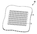
- a cross-sectional view of these conventional light emitting modules 40 and 50 is shown in FIG.
- the light extraction efficiency can be increased and the luminous flux can be increased as compared with the conventional bank type, line type, or lens type light emitting modules 30, 40, and 50. it can. Further, according to the present embodiment, the amount of a relatively expensive sealing member used can be reduced and the material cost can be reduced as compared with the conventional bank type light emitting module 30 and line type light emitting module 40. .
- each LED chip 2 can be individually sealed with a space therebetween, and thus such a problem of reabsorption occurs. Absent.
- the height of the side surface 4a of the sealing member 4 is determined based on the mounting height of the LED chip 2. Various changes were made, and the light emission characteristics of the light emitting module 10 in each case were measured. As a result, when the height t of the side surface 4a of the sealing member 4 is set to a value satisfying 0.4 ⁇ t / d ⁇ 1.5 with respect to the mounting height d of the LED chip 2, good characteristics are obtained. It turns out that it is obtained.
- the inter-chip pitch was variously changed based on the length of one side of the LED chip 2, and the light emission characteristics of the light emitting module 10 in each case were measured. As a result, it has been found that good characteristics can be obtained when the pitch is set to 2 to 3.5 times the length of one side of the LED chip 2.
- the pitch of the LED chips 2 when the pitch of the LED chips 2 is set to be twice or less the length of one side of the LED chip 2, the surfaces of the sealing member 4 that seals each LED chip 2 come close to each other, and one light emitting portion The white light and blue light emitted from 13 are reabsorbed by the other light emitting unit 13 adjacent thereto, and the light emission efficiency is reduced accordingly. Further, when the pitch of the LED chips 2 is set to be 3.5 times or more of the length of one side of the LED chip 2, although the light emission efficiency is hardly lowered, the light emitting area of the light emitting module 10 as a whole increases, and the lighting fixture 20 also becomes large. For this reason, it is desirable to set the pitch of the LED chips 2 to be larger than twice the length of one side of the LED chip 2 and smaller than 3.5 times.
- the diameter R of the sealing member 4 is variously changed on the basis of the diagonal length L of the LED chip 2, and the light emission of the light emitting module 10 in each case Characteristics were measured. As a result, good characteristics can be obtained when the diameter R of the sealing member 4 is set to a value satisfying 1.13 ⁇ R / L ⁇ 1.5 with respect to the diagonal length L of the LED chip 2. I understood.
- the present invention is not limited thereto, and the present invention may be applied to other lighting fixtures such as a light bulb and a ceiling light. .
- the light emitting module 10 having the flip chip type LED chip 2 has been described.
- the present invention is not limited to this, and the present invention can also be applied to a light emitting module having a face up type LED chip.
- the height of the side surface 4a of the sealing member 4 becomes higher than the height of the light emitting layer of the LED chip.
- the light emitting module and the lighting fixture of the embodiment can increase the light extraction efficiency and increase the luminous flux.
Landscapes
- Engineering & Computer Science (AREA)
- General Engineering & Computer Science (AREA)
- Non-Portable Lighting Devices Or Systems Thereof (AREA)
- Led Device Packages (AREA)
Abstract
Un mode de réalisation de la présente invention porte sur un module émetteur de lumière, lequel module a des éléments émetteurs de lumière à semi-conducteurs montés sur une surface de substrat, et des éléments d'encapsulation, qui encapsulent respectivement les éléments émetteurs de lumière à semi-conducteurs par intervalles sur la surface de substrat. La surface de chacun des éléments d'encapsulation ayant respectivement les éléments émetteurs de lumière à semi-conducteurs encapsulés à l'intérieur de ceux-ci comprend une surface latérale annulaire qui s'élève de façon linéaire dans la direction d'éloignement à partir de la surface de substrat, et une surface supérieure continue à partir de la surface latérale, ladite surface supérieure étant sur le côté séparé vis-à-vis de la surface de substrat.
Priority Applications (1)
| Application Number | Priority Date | Filing Date | Title |
|---|---|---|---|
| PCT/JP2011/071865 WO2013046292A1 (fr) | 2011-09-26 | 2011-09-26 | Module émetteur de lumière et appareil d'éclairage |
Applications Claiming Priority (1)
| Application Number | Priority Date | Filing Date | Title |
|---|---|---|---|
| PCT/JP2011/071865 WO2013046292A1 (fr) | 2011-09-26 | 2011-09-26 | Module émetteur de lumière et appareil d'éclairage |
Publications (1)
| Publication Number | Publication Date |
|---|---|
| WO2013046292A1 true WO2013046292A1 (fr) | 2013-04-04 |
Family
ID=47994411
Family Applications (1)
| Application Number | Title | Priority Date | Filing Date |
|---|---|---|---|
| PCT/JP2011/071865 WO2013046292A1 (fr) | 2011-09-26 | 2011-09-26 | Module émetteur de lumière et appareil d'éclairage |
Country Status (1)
| Country | Link |
|---|---|
| WO (1) | WO2013046292A1 (fr) |
Cited By (1)
| Publication number | Priority date | Publication date | Assignee | Title |
|---|---|---|---|---|
| CN107636390A (zh) * | 2015-03-20 | 2018-01-26 | 沙特基础工业全球技术公司 | 用于照明设备的塑料散热件 |
Citations (5)
| Publication number | Priority date | Publication date | Assignee | Title |
|---|---|---|---|---|
| JP2004172586A (ja) * | 2002-11-07 | 2004-06-17 | Matsushita Electric Ind Co Ltd | Led照明光源 |
| JP2006210490A (ja) * | 2005-01-26 | 2006-08-10 | Matsushita Electric Ind Co Ltd | 発光装置および発光装置の製造方法 |
| JP2008108952A (ja) * | 2006-10-26 | 2008-05-08 | Matsushita Electric Ind Co Ltd | 半導体発光装置および半導体発光装置の製造方法 |
| JP2008270314A (ja) * | 2007-04-17 | 2008-11-06 | Toyoda Gosei Co Ltd | 発光装置及び発光装置の製造方法 |
| JP2011159769A (ja) * | 2010-01-29 | 2011-08-18 | Mitsubishi Chemicals Corp | 半導体発光装置 |
-
2011
- 2011-09-26 WO PCT/JP2011/071865 patent/WO2013046292A1/fr active Application Filing
Patent Citations (5)
| Publication number | Priority date | Publication date | Assignee | Title |
|---|---|---|---|---|
| JP2004172586A (ja) * | 2002-11-07 | 2004-06-17 | Matsushita Electric Ind Co Ltd | Led照明光源 |
| JP2006210490A (ja) * | 2005-01-26 | 2006-08-10 | Matsushita Electric Ind Co Ltd | 発光装置および発光装置の製造方法 |
| JP2008108952A (ja) * | 2006-10-26 | 2008-05-08 | Matsushita Electric Ind Co Ltd | 半導体発光装置および半導体発光装置の製造方法 |
| JP2008270314A (ja) * | 2007-04-17 | 2008-11-06 | Toyoda Gosei Co Ltd | 発光装置及び発光装置の製造方法 |
| JP2011159769A (ja) * | 2010-01-29 | 2011-08-18 | Mitsubishi Chemicals Corp | 半導体発光装置 |
Cited By (3)
| Publication number | Priority date | Publication date | Assignee | Title |
|---|---|---|---|---|
| CN107636390A (zh) * | 2015-03-20 | 2018-01-26 | 沙特基础工业全球技术公司 | 用于照明设备的塑料散热件 |
| JP2018508111A (ja) * | 2015-03-20 | 2018-03-22 | サビック グローバル テクノロジーズ ベスローテン フェンノートシャップ | 照明器具のためのプラスチック製ヒートシンク |
| US10480768B2 (en) | 2015-03-20 | 2019-11-19 | Sabic Global Technologies B.V. | Plastic heat sink for luminaires |
Similar Documents
| Publication | Publication Date | Title |
|---|---|---|
| US20230184394A1 (en) | Led lamp | |
| JP5320560B2 (ja) | 光源ユニット及び照明装置 | |
| US7868345B2 (en) | Light emitting device mounting substrate, light emitting device housing package, light emitting apparatus, and illuminating apparatus | |
| JP2014139950A (ja) | ランプ及び照明装置 | |
| JP2011192703A (ja) | 発光装置及び照明装置 | |
| JP5993497B2 (ja) | Led照明装置 | |
| JP2007294621A (ja) | Led照明装置 | |
| US9443832B2 (en) | Light emitting device, light source for illumination, and illumination apparatus | |
| US10490721B2 (en) | Light-emitting device and illuminating apparatus | |
| TW201334227A (zh) | 發光模組 | |
| JP2012243643A (ja) | 電球形ランプ及び照明装置 | |
| JP2011134934A (ja) | 発光モジュールおよび照明装置 | |
| KR100634301B1 (ko) | 발광다이오드 | |
| JP2015133455A (ja) | 発光装置、照明用光源、および照明装置 | |
| JP2011181252A (ja) | 照明器具 | |
| WO2013046292A1 (fr) | Module émetteur de lumière et appareil d'éclairage | |
| JP5569759B2 (ja) | 光源ユニット | |
| JP4601404B2 (ja) | 発光装置および照明装置 | |
| JP2012142167A (ja) | ランプ及び照明装置 | |
| JP2014013924A (ja) | 発光モジュールおよび照明装置 | |
| JP2013073983A (ja) | 発光装置及び照明装置 | |
| JP2019087570A (ja) | 発光装置およびledパッケージ | |
| JP2018120962A (ja) | 発光装置、及び、照明装置 | |
| JP2018022733A (ja) | 発光装置、照明用光源及び照明装置 | |
| JP2015133450A (ja) | 発光装置、照明用光源、および照明装置 |
Legal Events
| Date | Code | Title | Description |
|---|---|---|---|
| 121 | Ep: the epo has been informed by wipo that ep was designated in this application |
Ref document number: 11873405 Country of ref document: EP Kind code of ref document: A1 |
|
| NENP | Non-entry into the national phase |
Ref country code: DE |
|
| 122 | Ep: pct application non-entry in european phase |
Ref document number: 11873405 Country of ref document: EP Kind code of ref document: A1 |
|
| NENP | Non-entry into the national phase |
Ref country code: JP |