WO2013046292A1 - Light emitting module and illuminating apparatus - Google Patents
Light emitting module and illuminating apparatus Download PDFInfo
- Publication number
- WO2013046292A1 WO2013046292A1 PCT/JP2011/071865 JP2011071865W WO2013046292A1 WO 2013046292 A1 WO2013046292 A1 WO 2013046292A1 JP 2011071865 W JP2011071865 W JP 2011071865W WO 2013046292 A1 WO2013046292 A1 WO 2013046292A1
- Authority
- WO
- WIPO (PCT)
- Prior art keywords
- light emitting
- emitting module
- light
- sealing member
- substrate
- Prior art date
- Legal status (The legal status is an assumption and is not a legal conclusion. Google has not performed a legal analysis and makes no representation as to the accuracy of the status listed.)
- Ceased
Links
Images


Classifications
-
- F—MECHANICAL ENGINEERING; LIGHTING; HEATING; WEAPONS; BLASTING
- F21—LIGHTING
- F21S—NON-PORTABLE LIGHTING DEVICES; SYSTEMS THEREOF; VEHICLE LIGHTING DEVICES SPECIALLY ADAPTED FOR VEHICLE EXTERIORS
- F21S8/00—Lighting devices intended for fixed installation
- F21S8/02—Lighting devices intended for fixed installation of recess-mounted type, e.g. downlighters
- F21S8/026—Lighting devices intended for fixed installation of recess-mounted type, e.g. downlighters intended to be recessed in a ceiling or like overhead structure, e.g. suspended ceiling
-
- F—MECHANICAL ENGINEERING; LIGHTING; HEATING; WEAPONS; BLASTING
- F21—LIGHTING
- F21V—FUNCTIONAL FEATURES OR DETAILS OF LIGHTING DEVICES OR SYSTEMS THEREOF; STRUCTURAL COMBINATIONS OF LIGHTING DEVICES WITH OTHER ARTICLES, NOT OTHERWISE PROVIDED FOR
- F21V29/00—Protecting lighting devices from thermal damage; Cooling or heating arrangements specially adapted for lighting devices or systems
- F21V29/85—Protecting lighting devices from thermal damage; Cooling or heating arrangements specially adapted for lighting devices or systems characterised by the material
-
- F—MECHANICAL ENGINEERING; LIGHTING; HEATING; WEAPONS; BLASTING
- F21—LIGHTING
- F21Y—INDEXING SCHEME ASSOCIATED WITH SUBCLASSES F21K, F21L, F21S and F21V, RELATING TO THE FORM OR THE KIND OF THE LIGHT SOURCES OR OF THE COLOUR OF THE LIGHT EMITTED
- F21Y2105/00—Planar light sources
- F21Y2105/10—Planar light sources comprising a two-dimensional [2D] array of point-like light-generating elements
-
- F—MECHANICAL ENGINEERING; LIGHTING; HEATING; WEAPONS; BLASTING
- F21—LIGHTING
- F21Y—INDEXING SCHEME ASSOCIATED WITH SUBCLASSES F21K, F21L, F21S and F21V, RELATING TO THE FORM OR THE KIND OF THE LIGHT SOURCES OR OF THE COLOUR OF THE LIGHT EMITTED
- F21Y2115/00—Light-generating elements of semiconductor light sources
- F21Y2115/10—Light-emitting diodes [LED]
-
- H—ELECTRICITY
- H10—SEMICONDUCTOR DEVICES; ELECTRIC SOLID-STATE DEVICES NOT OTHERWISE PROVIDED FOR
- H10H—INORGANIC LIGHT-EMITTING SEMICONDUCTOR DEVICES HAVING POTENTIAL BARRIERS
- H10H20/00—Individual inorganic light-emitting semiconductor devices having potential barriers, e.g. light-emitting diodes [LED]
- H10H20/80—Constructional details
- H10H20/85—Packages
- H10H20/852—Encapsulations
- H10H20/853—Encapsulations characterised by their shape
Definitions
- Embodiments of the present invention relate to a light emitting module in which a semiconductor light emitting element such as an LED (light emitting diode) is mounted on a substrate, and a lighting fixture incorporating the light emitting module.
- a semiconductor light emitting element such as an LED (light emitting diode) is mounted on a substrate
- a lighting fixture incorporating the light emitting module.
- a lens type in which a plurality of LEDs arranged side by side on a substrate are individually sealed with a sealing member, a line type in which a plurality of LEDs are arranged in a row and sealed, or a frame surrounding a plurality of LEDs A bank type in which a (bank) is provided and a plurality of LEDs are sealed together is generally known.
- the sealing member that seals the LED to the substrate is a translucent material including phosphor particles that excite and emit light having a complementary color relationship with the emission color of the LED, and light emitted directly from the LED. Mix to emit white light.
- a sealing member that includes a phosphor that is excited by blue light and emits yellow light or red light is sealed with a sealing member that includes a phosphor that is excited by blue light and emits yellow light or red light.
- the light-emitting module includes a plurality of semiconductor light-emitting elements mounted on the substrate surface, and a sealing member that seals the semiconductor light-emitting elements on the substrate surface at intervals.
- the surface of the sealing member that individually seals the semiconductor light emitting element includes a side surface that rises linearly in a direction away from the substrate surface, and a top surface that is continuous with the side surface on the side away from the substrate surface.
- the light extraction efficiency can be increased.
- FIG. 1 is a sectional view of the lighting fixture concerning an embodiment.
- FIG. 2 is a front view of the lighting apparatus of FIG. 1 as viewed from the light extraction side.
- FIG. 3 is a perspective view of the light emitting module according to the embodiment as viewed from the light extraction side. 4 is a partially enlarged cross-sectional view of the light emitting module of FIG.
- FIG. 5 is a cross-sectional view showing a mounted state of the LED chip incorporated in the light emitting module of FIG.
- FIG. 6 is a cross-sectional view showing a modification of the sealing member in which the LED chip of the light emitting module of FIG. 3 is sealed.
- FIG. 7 is a cross-sectional view showing another modification of the sealing member in which the LED chip of the light emitting module of FIG.
- FIG. 8 is a perspective view of a conventional bank type light emitting module as seen from the light extraction side.
- FIG. 9 is a partially enlarged cross-sectional view of the light emitting module of FIG.
- FIG. 10 is a perspective view of a conventional line type light emitting module as seen from the light extraction side.
- FIG. 11 is a perspective view of a conventional lens-type light emitting module as seen from the light extraction side.
- 12 is a partially enlarged cross-sectional view of the light emitting module of FIGS.
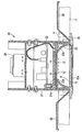
- Drawing 1 is a sectional view of lighting fixture 20 concerning an embodiment.
- FIG. 2 is the front view which looked at this lighting fixture 20 from the light extraction side.
- the lighting fixture 20 is a downlight using a light emitting module 10 described later as a light source, and includes a case 21 to which the light emitting module 10 is attached and a lighting device 22 that lights the light emitting module 10.
- the case 21 is made of, for example, aluminum die casting and has a cylindrical shape having openings at both ends, and integrally includes a mounting plate 21a for mounting the light emitting module 10 therein.
- the light emitting module 10 is attached to the case 21 by fastening the substrate 11 to the attachment plate 21a with screws. At this time, the copper metal member 14 provided on the back surface of the substrate 11 is in close contact with the flat surface of the aluminum mounting plate 21a. As a result, heat generated from each light emitting unit 13 (to be described later) of the light emitting module 10 is efficiently radiated to the mounting plate 21 a through the substrate 11 and the metal member 14.
- the reflector 23 is attached to the inside of the case 21 on the surface side of the light emitting module 10.
- the reflector 23 is made of a white synthetic resin having light resistance, heat resistance and electrical insulation, for example, polybutylene terephthalate (PBT).
- PBT polybutylene terephthalate
- the reflector 23 has a circular opening 23a that surrounds the plurality of light emitting portions 13, and a so-called “mortar-shaped” reflecting surface 23b that expands from the edge of the opening 23a.
- the lighting device 22 includes a lighting circuit and a power supply circuit for lighting the plurality of light emitting units 13 of the light emitting module 10.
- the lighting device 22 converts an AC voltage of 100 V obtained from a commercial power source into a DC voltage of 24 V, and supplies a constant DC current to each light emitting unit 13.
- the lighting device 22 is housed inside the case 21.
- a power terminal block 24 for supplying power from the commercial power source to the lighting device 22 is provided at the end of the case 21 on the side opposite to the light extraction side.
- a decorative frame 25 is attached to the end of the case 21 on the light extraction side.
- the decorative frame 25 is adjacent to the light emitting area where the plurality of light emitting units 13 are arranged, and is covered with a transparent cover member 25a.
- a support 26 for holding the case 21 on the ceiling X is attached to the end of the case 21 on the light extraction side.
- the support 26 is a leaf spring.
- the power line wired in the installation hole H formed in the ceiling X is connected to the power terminal block 24.
- the support tool 26 is bent inward by hand, and the tip is inserted into the installation hole H together with the case 21, and then the hand is released from the support tool 26.
- the support 26 is restored by its own elasticity and pressed against the inner surface of the installation hole H, and the decorative frame 25 is brought into contact with the ceiling X so as to sandwich the ceiling X between the support 26 and the support X.
- the edge of the installation hole H is covered with the decorative frame 25.
- each light emitting unit 13 When the lighting fixture 20 having the above structure is turned on, most of the light emitted from each light emitting unit 13 is reflected directly or by the reflection surface 23b of the reflector 23 and spreads downward and radiated. At this time, part of the light emitted from the light emitting unit 13 is also reflected on the wiring pattern on the substrate surface and the substrate surface.
- the surface of the wiring pattern is plated with nickel, silver, gold or the like.
- the substrate 11 is made of white ceramics. For this reason, the light is well reflected on the surface of the wiring pattern and the surface of the substrate 11 so that the entire lighting fixture 20 can maintain a desired light emission amount.
- the LED chip 2 of each light emitting unit 13 when the lighting fixture 20 is turned on as described above, the LED chip 2 of each light emitting unit 13 generates heat. In order to prevent deterioration over time due to heat of the light emitting unit 13, it is necessary to efficiently dissipate this heat.
- the metal member 14 attached to the back side of the substrate 11 is made of copper having excellent thermal conductivity
- the substrate 11 itself is made of ceramics having good thermal conductivity
- the case 21 is also made of Since it is formed of aluminum having excellent thermal conductivity, the heat generated from the light emitting portion 13 is transmitted from the wiring pattern 12 to the metal member 14 through the insulating substrate 11, and further, the heat transfer surface of the mounting plate 21a. Is transmitted to the case 21 via.
- the heat transmitted to the case 21 is radiated to the outside of the lighting fixture 20. That is, the heat from each light emitting part 13 is effectively radiated to the outside from the side wall of the case 21 having a large surface area.
- the lighting fixture 20 of this embodiment suppresses a decrease in the light conversion efficiency of each light-emitting unit 13 by the above-described heat dissipation action, and performs illumination with bright illuminance. Moreover, the lifetime of the light emission part 13 is also extended by the above-mentioned heat dissipation action.
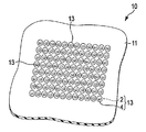
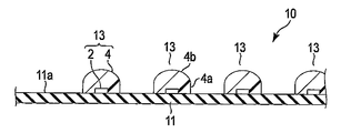
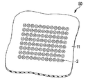
- FIG. 3 is a perspective view of the light emitting module 10 of this embodiment incorporated in the lighting fixture 20 as seen from the light extraction side.
- FIG. 4 is a partially enlarged cross-sectional view of the light emitting module 10 of FIG. 1 and 2, the light emitting module 10 having 25 light emitting units 13 has been described. However, the number of the light emitting units 13 may be any number, and at least one may be used. Here, 96 light emitting units 13 are provided. The light emitting module 10 having the above will be described.
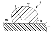
- the light emitting module 10 includes a substrate 11 having a wiring pattern (not shown) on the surface, a plurality of LED chips 2 (semiconductor light emitting elements) mounted on the surface 11a of the substrate 11 and electrically connected to the wiring pattern, And it has the some sealing member 4 which seals each LED chip 2 on the surface 11a of the board
- Each LED chip 2 and the sealing member 4 that seals it constitute the light emitting unit 13 described above.
- the substrate 11 is a DCB (Direct Copper Bonding) substrate, DBA (Direct Brazing Aluminum) substrate, AMC (Active Metal Brazed Copper) substrate, DPC (Direct Plated Copper) substrate, metal substrate, ceramic substrate, glass epoxy substrate, or the like.
- the DCB substrate is formed by directly bonding a copper plate to a ceramic base material.
- the DBA substrate is formed by brazing an aluminum plate on a ceramic base material.
- the AMC substrate is formed by brazing a copper plate on a ceramic base material.
- the DPC board is a ceramic base material plated with copper. Incidentally, it is possible to use as a ceramic substrate, Al 2 O 3, AlN, etc. Si 3 N 4.
- a wiring pattern (not shown) is provided on the surface 11 a of the substrate 11.
- the wiring pattern is formed by etching copper provided on the substrate surface 11a and patterning the gold pattern or silver plating on the copper pattern via nickel plating.
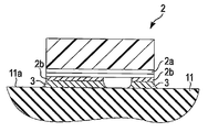
- the LED chip 2 of this embodiment is of a type that is flip-chip connected to the substrate surface 11a, and the light emitting layer 2a is close to the substrate surface 11a.
- Each LED chip 2 has a bump 2b for connecting to the wiring pattern.
- the LED chip 2 is connected to the wiring pattern on the substrate surface 11a by eutectic solder 3, for example.
- silver paste or gold bumps may be used.
- the LED chip 2 of the present embodiment is a blue light emitting diode that emits blue light when energized.
- the sealing member 4 is a translucent resin containing a phosphor.
- the sealing member 4 including a phosphor that is excited by blue light and emits yellow light and red light is used.
- the sealing member 4 is provided on the substrate surface 11 a so as to cover the entire surface of the LED chip 2.
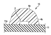
- the shape of the sealing member 4 is designed such that the surface thereof includes a side surface 4a that rises linearly in a direction away from the substrate surface 11a, and a top surface 4b that is continuous with the side surface 4a on the side away from the substrate surface 11a.
- This shape is a so-called bullet shape.
- the side surface 4a may be substantially perpendicular to the substrate surface 11a.
- the side surface 4a may be inclined slightly inward toward the substrate surface 11a (downward in the drawing).
- it may be slightly inclined outward toward the substrate surface 11a. That is, the expression “rising up in a straight line” described above includes those in FIGS. 6 and 7.
- the sealing member 4 is formed by resin injection molding, it is desirable to design the sealing member 4 so as to slightly widen the bottom of the sealing member 4 as shown in FIG.
- the top surface 4b is not limited to a spherical surface, and may be any shape as long as it can increase the light emission efficiency, such as a flat surface, a concave surface, or a concave and convex surface. You can choose. For example, when it is desired to reduce the luminous intensity of the central part and spread the light to the peripheral part, it is preferable to use a concave surface, and to increase the degree of color mixing of the light emitted from the sealing member 4, it is preferable to use an uneven surface.
- the shape of the top surface 4b is, for example, a spherical shape that is smoothly continuous with an end portion (upper end in the drawing) of the side surface 4a that is spaced from the substrate surface 11a. preferable.
- the LED chip 2 of the present embodiment has a flat rectangular block shape, is a square having a side length of 1 mm, and a mounting height from the substrate surface 11a is 0.17 mm.
- 96 LED chips 2 are arranged 8 ⁇ 12 vertically and horizontally on the substrate surface 11a. At this time, the pitch of each LED chip 2 was set to 3.0 mm in length and 2.5 mm in width.
- the sealing member 4 of the present embodiment has the above-mentioned bullet shape, its side surface 4a has a cylindrical shape with a diameter of 1.7 mm and a height of 0.41 mm, and its top surface 4b has a curvature radius of 1.1 mm. It is made spherical. In this case, the height of the sealing member 4 including the top surface 4b from the substrate surface 11a is about 1 mm.
- the sealing member 4 since the sealing member 4 has the side surface 4a that rises substantially perpendicularly from the substrate surface 11a, in addition to the light directly emitted through the side surface 4a, the light toward the substrate surface 11a and the side surface 4a A large amount of light that is effective for illumination in the light extraction direction, such as light that is reflected on the inside and emitted through the top surface 4b, can be extracted.
- the light extraction efficiency can be further increased. That is, at a pitch at which light emitted from one light emitting unit 13 through the sealing member 4 is not absorbed by the sealing member 4 of the adjacent light emitting unit 13 and does not cause luminance unevenness. It is desirable to design.
- each part of the light emitting part 13 it is desirable to mount the LED chip 2 on the substrate surface 11a as in the present embodiment.
- the face-up type LED chip is wire-bonded to the wiring pattern on the substrate surface, it is necessary to connect the bonding wire by arranging an electrode pad at the end of the chip on the light extraction side, resulting in a decrease in luminous efficiency. At the same time, the diameter of the sealing member is increased.
- the light emitted from the LED chip 2 may be absorbed before exiting the sealing member, and the light emission efficiency may be decreased accordingly.
- the pitch between the chips is not changed, the distance between the sealing member surfaces in the adjacent light emitting parts is shortened, and light is reabsorbed by the adjacent light emitting parts, and the luminous efficiency is accordingly increased. descend.
- the diameter of the sealing member is increased, the material cost is increased accordingly, and the module is also increased in size.
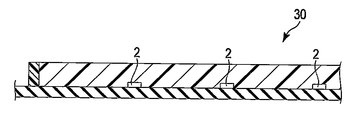
- the light emitting module 30 has a structure in which a bank 32 surrounding all the LED chips 2 arranged in the vertical and horizontal directions is provided, and a sealing member 34 is filled in the bank 32 to seal all the LED chips 2.
- Other structures have the same structure as the light emitting module 10 of the above-described embodiment.
- the conventional bank type light emitting module 30 emitted light at a correlated color temperature of 5037K, and a light flux of 10900 lm was obtained.
- the light emitting module 10 using the bullet-shaped sealing member 4 of the present embodiment emitted light with a correlated color temperature of 4967K, and a light flux of 14000 lm was obtained. That is, when the light emitting module 10 of the present embodiment and the conventional light emitting module 30 are lit under the same conditions, the light emitting module 10 using the shell-shaped sealing member 4 of the present embodiment is different from the conventional bank type. The light extraction efficiency of 1.29 times could be obtained.
- the luminous flux was 8409lm at the correlated color temperature 5043K
- the lens type light emitting module 50 the luminous flux was 9423lm at the correlated color temperature 5018K.
- a cross-sectional view of these conventional light emitting modules 40 and 50 is shown in FIG.
- the light extraction efficiency can be increased and the luminous flux can be increased as compared with the conventional bank type, line type, or lens type light emitting modules 30, 40, and 50. it can. Further, according to the present embodiment, the amount of a relatively expensive sealing member used can be reduced and the material cost can be reduced as compared with the conventional bank type light emitting module 30 and line type light emitting module 40. .
- each LED chip 2 can be individually sealed with a space therebetween, and thus such a problem of reabsorption occurs. Absent.
- the height of the side surface 4a of the sealing member 4 is determined based on the mounting height of the LED chip 2. Various changes were made, and the light emission characteristics of the light emitting module 10 in each case were measured. As a result, when the height t of the side surface 4a of the sealing member 4 is set to a value satisfying 0.4 ⁇ t / d ⁇ 1.5 with respect to the mounting height d of the LED chip 2, good characteristics are obtained. It turns out that it is obtained.
- the inter-chip pitch was variously changed based on the length of one side of the LED chip 2, and the light emission characteristics of the light emitting module 10 in each case were measured. As a result, it has been found that good characteristics can be obtained when the pitch is set to 2 to 3.5 times the length of one side of the LED chip 2.
- the pitch of the LED chips 2 when the pitch of the LED chips 2 is set to be twice or less the length of one side of the LED chip 2, the surfaces of the sealing member 4 that seals each LED chip 2 come close to each other, and one light emitting portion The white light and blue light emitted from 13 are reabsorbed by the other light emitting unit 13 adjacent thereto, and the light emission efficiency is reduced accordingly. Further, when the pitch of the LED chips 2 is set to be 3.5 times or more of the length of one side of the LED chip 2, although the light emission efficiency is hardly lowered, the light emitting area of the light emitting module 10 as a whole increases, and the lighting fixture 20 also becomes large. For this reason, it is desirable to set the pitch of the LED chips 2 to be larger than twice the length of one side of the LED chip 2 and smaller than 3.5 times.
- the diameter R of the sealing member 4 is variously changed on the basis of the diagonal length L of the LED chip 2, and the light emission of the light emitting module 10 in each case Characteristics were measured. As a result, good characteristics can be obtained when the diameter R of the sealing member 4 is set to a value satisfying 1.13 ⁇ R / L ⁇ 1.5 with respect to the diagonal length L of the LED chip 2. I understood.
- the present invention is not limited thereto, and the present invention may be applied to other lighting fixtures such as a light bulb and a ceiling light. .
- the light emitting module 10 having the flip chip type LED chip 2 has been described.
- the present invention is not limited to this, and the present invention can also be applied to a light emitting module having a face up type LED chip.
- the height of the side surface 4a of the sealing member 4 becomes higher than the height of the light emitting layer of the LED chip.
- the light emitting module and the lighting fixture of the embodiment can increase the light extraction efficiency and increase the luminous flux.
Landscapes
- Engineering & Computer Science (AREA)
- General Engineering & Computer Science (AREA)
- Non-Portable Lighting Devices Or Systems Thereof (AREA)
- Led Device Packages (AREA)
Abstract
Description
本発明の実施形態は、LED(発光ダイオード)等の半導体発光素子を基板に実装した発光モジュール、およびこの発光モジュールを組み込んだ照明器具に関する。 Embodiments of the present invention relate to a light emitting module in which a semiconductor light emitting element such as an LED (light emitting diode) is mounted on a substrate, and a lighting fixture incorporating the light emitting module.
近年、LEDを基板に実装した発光モジュールや、この発光モジュールを組み込んだ照明器具が普及されつつある。 In recent years, a light-emitting module in which an LED is mounted on a substrate and a lighting apparatus incorporating the light-emitting module are becoming popular.
発光モジュールとして、基板上に並べて配列した複数個のLEDを個々に封止部材で封止したレンズタイプ、複数個のLEDを1列に並べて封止したラインタイプ、或いは複数個のLEDを囲む枠(バンク)を設け、複数のLEDをまとめて封止したバンクタイプなどが一般に知られている。 As a light emitting module, a lens type in which a plurality of LEDs arranged side by side on a substrate are individually sealed with a sealing member, a line type in which a plurality of LEDs are arranged in a row and sealed, or a frame surrounding a plurality of LEDs A bank type in which a (bank) is provided and a plurality of LEDs are sealed together is generally known.
通常、LEDを基板に封止する封止部材は、LEDの発光色と補色の関係にある光を励起発光する蛍光体粒子を含んだ透光性材料であり、LEDから直接放出される光と混ぜて白色光を放出する。例えば、青色光を発光するLEDを、青色光で励起されて黄色光や赤色光を発光する蛍光体を含む封止部材で封止する。 Usually, the sealing member that seals the LED to the substrate is a translucent material including phosphor particles that excite and emit light having a complementary color relationship with the emission color of the LED, and light emitted directly from the LED. Mix to emit white light. For example, an LED that emits blue light is sealed with a sealing member that includes a phosphor that is excited by blue light and emits yellow light or red light.
しかし、現状では、上述した各タイプの発光モジュールにおいて、十分に満足のいく光束を得るには至っていない。また、光取出し効率も十分に満足のいくものではない。 However, at present, the above-mentioned types of light emitting modules have not yet obtained a sufficiently satisfactory luminous flux. Also, the light extraction efficiency is not fully satisfactory.
よって、光取出し効率が高い発光モジュール、および照明器具の開発が望まれている。 Therefore, it is desired to develop a light emitting module and a lighting fixture with high light extraction efficiency.
実施形態に係る発光モジュールは、基板表面に実装された複数個の半導体発光素子、およびこの半導体発光素子を基板表面に個別に間隔を開けて封止した封止部材を有する。半導体発光素子を個別に封止した封止部材の表面は、基板表面から離れる方向に直線状に立ち上がる側面、および基板表面から離間した側で側面に連続した頂面を含む。 The light-emitting module according to the embodiment includes a plurality of semiconductor light-emitting elements mounted on the substrate surface, and a sealing member that seals the semiconductor light-emitting elements on the substrate surface at intervals. The surface of the sealing member that individually seals the semiconductor light emitting element includes a side surface that rises linearly in a direction away from the substrate surface, and a top surface that is continuous with the side surface on the side away from the substrate surface.
実施形態に係る発光モジュール、および照明器具によると、光取出し効率を高くすることができる。 According to the light emitting module and the lighting fixture according to the embodiment, the light extraction efficiency can be increased.
以下、図面を参照しながら実施形態について詳細に説明する。
図1は、実施形態に係る照明器具20の断面図である。また、図2は、この照明器具20を光の取り出し側から見た正面図である。
Hereinafter, embodiments will be described in detail with reference to the drawings.
この照明器具20は、後述する発光モジュール10を光源としたダウンライトであって、発光モジュール10を取り付けたケース21、および発光モジュール10を点灯させる点灯装置22を有する。ケース21は、例えばアルミダイカスト製で、両端部に開口を有する円筒形であり、その内部に発光モジュール10を取り付けるための取付板21aを一体に有する。
The
発光モジュール10は、基板11をネジにより取付板21aに締結固定することで、ケース21に取り付けられる。この際、基板11の裏面に設けられた銅製の金属部材14がアルミニウム製の取付板21aの平坦な面に密着する。これにより、発光モジュール10の後述する各発光部13から発生される熱が、基板11および金属部材14を通して取付板21aに効率よく放熱されるようになる。
The
反射体23は、発光モジュール10の表面側で、ケース21の内側に取り付けられる。反射体23は、耐光性、耐熱性および電気絶縁性を有する白色の合成樹脂、例えば、ポリブチレンテレフタレート(PBT)等で構成される。反射体23は、複数個の発光部13を囲む円形の開口部23a、および開口部23aの縁から拡開したいわゆる「すり鉢状」の反射面23bを有する。
The
点灯装置22は、発光モジュール10の複数個の発光部13を点灯させるための点灯回路および電源回路を有する。点灯装置22は、商用電源から得られる100Vの交流電圧を24Vの直流電圧に変換し、各発光部13に一定の直流電流を供給する。この点灯装置22は、ケース21の内部に収納される。
The
点灯装置22に商用電源からの電力を供給するための電源端子台24は、光の取り出し側とは反対側で、ケース21の端部に設けられている。
A
ケース21の光の取り出し側の端部には、化粧枠25が取り付けられている。化粧枠25は、複数の発光部13が配置された発光領域に隣接しており、透明なカバー部材25aによって覆われている。
A
また、ケース21の光の取り出し側の端部には、ケース21を天井Xに保持するための支持具26が取り付けられている。この支持具26は、板バネである。
Further, a
上記構造の照明器具20を天井Xに取り付ける場合、まず、天井Xに形成された設置孔Hに配線された電源線を電源端子台24に接続する。そして、支持具26を手で内方に撓ませ、その先端をケース21と共に設置孔Hに挿入したのち、支持具26から手を放す。これにより、支持具26が自らの弾性により復元して設置孔Hの内面に圧接し、支持具26との間に天井Xを挟むように化粧枠25が天井Xに当接される。この状態で、設置孔Hの縁は、化粧枠25によって覆われる。
When attaching the
上記構造の照明器具20を点灯すると、各発光部13から出射された光の多くは、直接、或いは反射体23の反射面23bで反射されて、下向きに広がって放射される。この際、発光部13から放射された光の一部は、基板表面の配線パターンや基板表面でも反射される。配線パターンは、ニッケル、銀、金などで表面がメッキされている。また、基板11は、白色のセラミックスで構成されている。このため、配線パターンの表面や基板11の表面でも光が良好に反射され、照明器具20全体として所望の発光量を保つことができるようになっている。
When the
また、上記のように照明器具20を点灯させると、各発光部13のLEDチップ2が発熱する。発光部13の熱による経時的な劣化を防止するため、この熱を効率良く放熱させる必要がある。本実施形態では、基板11の裏面側に貼り付けた金属部材14が熱伝導性に優れた銅製であるとともに、基板11自体も良好な熱伝導性を有するセラミックス製であり、さらに、ケース21も熱伝導性に優れたアルミニウムで形成されているため、発光部13から発生した熱は、配線パターン12から絶縁性の基板11を通って金属部材14へ伝達され、さらに取付板21aの熱伝達面を介してケース21に伝達される。そして、ケース21に伝達された熱は、照明器具20の外部へ放熱される。つまり、各発光部13からの熱は、表面積の大きなケース21の側壁から、効果的に外部に放熱されることになる。
Further, when the
以上のように、本実施形態の照明器具20は、上述の放熱作用によって、各発光部13の光変換効率の低下を抑制し、照度の明るい照明を行なう。また、上述の放熱作用によって、発光部13の寿命も延びる。
As described above, the
図3は、上記照明器具20に組み込まれた本実施形態の発光モジュール10を光の取り出し側から見た斜視図である。また、図4は、図3の発光モジュール10の部分拡大断面図である。図1および図2では、25個の発光部13を有する発光モジュール10について説明したが、発光部13の個数はいくつでも良く、少なくとも1つあれば良く、ここでは、96個の発光部13を有する発光モジュール10について説明する。
FIG. 3 is a perspective view of the
発光モジュール10は、表面に配線パターン(図示せず)を有する基板11、この基板11の表面11aに実装されて配線パターンに電気的に接続される複数個のLEDチップ2(半導体発光素子)、および各LEDチップ2を基板11の表面11aに個別に間隔を開けて封止する複数の封止部材4を有する。各LEDチップ2およびそれを封止した封止部材4は、上述した発光部13を構成している。
The
基板11は、DCB(Direct Copper Bonding)基板、DBA(Direct Brazing Aluminum)基板、AMC(Active Metal Brazed Copper)基板、DPC(Direct Plated Copper)基板、メタル基板、セラミック基板、ガラスエポキシ基板などである。DCB基板は、セラミックス基材に銅板を直接接合して形成されたものである。DBA基板は、セラミックス基材にアルミニウム板を蝋着して形成されたものである。AMC基板は、セラミックス基材に銅板を蝋着して形成されたものである。DPC基板は、セラミック基材に銅をメッキ成長させたものである。なお、セラミック基材として、Al2O3、AlN、Si3N4などを用いることができる。
The
基板11の表面11aには、図示しない配線パターンが設けられている。配線パターンは、基板表面11aに設けた銅をエッチングしてパターン化し、この銅パターン上にニッケルメッキを介して金メッキ或いは銀メッキをして形成される。
A wiring pattern (not shown) is provided on the
本実施形態のLEDチップ2は、図5に示すように、基板表面11aにフリップチップ接続されるタイプのものであり、発光層2aが基板表面11aに近接している。また、各LEDチップ2は、配線パターンに接続するためのバンプ2bを有する。LEDチップ2は、例えば、共晶はんだ3によって基板表面11aの配線パターンに接続される。この他に、銀ペーストや金バンプなどを用いても良い。なお、本実施形態のLEDチップ2は、通電により青色光を発光する青色発光ダイオードである。
As shown in FIG. 5, the
封止部材4は、蛍光体を含む透光性の樹脂である。本実施形態では、青色発光するLEDチップ2を用いたため、青色光によって励起されて黄色光と赤色光とを発光する蛍光体を含む封止部材4を用いた。封止部材4は、LEDチップ2の表面を全て覆うように基板表面11aに設けられる。
The sealing
この封止部材4の形状は、その表面が、基板表面11aから離れる方向に直線状に立ち上がった側面4a、および基板表面11aから離間した側で側面4aに連続した頂面4bを含む形状に設計されている。この形状は、いわゆる砲弾形である。
The shape of the sealing
側面4aは、基板表面11aに対して略垂直であれば良く、例えば、図6に示すように、基板表面11aに向けて(図示下方に向けて)僅かに内側に傾斜しても良く、図7に示すように、基板表面11aに向けて僅かに外側に傾斜しても良い。つまり、上述した「直線状に立ち上がる」という表現には、図6や図7のものも含まれる。特に、この封止部材4を樹脂の射出成形によって形成する場合、図7のように封止部材4の裾を僅かに広げる形状に設計することが望ましい。
The
また、頂面4bは、球面に限らず、平面、凹面、凸凹面など、発光効率を高めることができるものであれば、いかなる形状であってもよいが、所望の配光を得るために適宜選択することができる。例えば、中心部の光度を落とし、周辺部に光を広げたい場合には、凹面とし、封止部材4から出射する光の混色度合を高める場合には、凸凹面などにするとよい。しかしながら、頂面4bの形状は、側面4aの基板表面11aから離間した端部(図示上端)に滑らかに連続する例えば球面形状であることが、配光制御や製造性及び光取出し効率の点から好ましい。
In addition, the
ここで、本実施形態の発光モジュール10の各構成要素の具体的な寸法、形状、配置などについて説明する。
本実施形態のLEDチップ2は、偏平な矩形ブロック状であり、1辺の長さが1mmの正方形で基板表面11aからの実装高さが0.17mmである。本実施形態では、96個のLEDチップ2を縦横に8×12個ずつ並べて基板表面11a上に配置した。この際、各LEDチップ2のピッチは、縦3.0mm、横2.5mmに設定した。
Here, specific dimensions, shapes, arrangements, and the like of the respective components of the
The
本実施形態の封止部材4は、上述した砲弾形であり、その側面4aは、直径1.7mm、高さ0.41mmの円筒形であり、その頂面4bは、曲率半径1.1mmの球面にされている。この場合、頂面4bを含む封止部材4の基板表面11aからの高さは、1mm程度となる。
The sealing
以上のように、封止部材4が基板表面11aから略垂直に立ち上がる側面4aを有することで、この側面4aを介して直接放出される光に加え、基板表面11aに向かう光や、側面4aの内側で反射されて頂面4bを介して放出される光など、光の取り出し方向に向かう照明に有効な光を多く取り出すことができる。
As described above, since the sealing
また、上述した砲弾形の封止部材4を採用した上で、LEDチップ2同士のピッチを一定のピッチに設計することで、光の取り出し効率をより高めることができる。つまり、封止部材4を介して1つの発光部13から放出される光が隣接する発光部13の封止部材4に吸収されることのないピッチで、且つ輝度斑を生じることのないピッチに設計することが望ましい。
In addition, by adopting the above-described bullet-shaped
さらに、発光部13の各部の寸法を所望する寸法に設計するため、本実施形態のようにLEDチップ2を基板表面11aにフリップチップ実装することが望ましい。
Furthermore, in order to design each part of the
仮に、フェースアップタイプのLEDチップを基板表面の配線パターンにワイヤーボンディングする場合、チップの光の取り出し側の端部に電極パッドを配置してボンディングワイヤーを接続する必要があり、発光効率が低下するとともに、封止部材の径が大きくなってしまう。 If the face-up type LED chip is wire-bonded to the wiring pattern on the substrate surface, it is necessary to connect the bonding wire by arranging an electrode pad at the end of the chip on the light extraction side, resulting in a decrease in luminous efficiency. At the same time, the diameter of the sealing member is increased.
このように、封止部材の径が大きくなると、LEDチップ2から放出された光が封止部材から出る前に吸収されてしまうことが考えられ、その分、発光効率が低下することが考えられる。また、同時に、チップ間ピッチを変えない場合、隣接する発光部同士における封止部材表面間の距離が短くなり、隣接する発光部に光が再吸収されることになり、その分、発光効率が低下する。さらに、封止部材の径が大きくなると、その分、材料コストも高くなり、モジュールも大型化する。
As described above, when the diameter of the sealing member is increased, the light emitted from the
上述した本実施形態の発光モジュール10の特性を調べるため、図8および図9に示すような従来のバンクタイプの発光モジュール30を比較のため試作した。この発光モジュール30は、縦横に並べた全てのLEDチップ2を囲むバンク32を設け、このバンク32内に封止部材34を充填して全てのLEDチップ2を封止した構造を有する。これ以外の構造は、上述した実施形態の発光モジュール10と同じ構造を有する。
In order to investigate the characteristics of the
そして、本実施形態の発光モジュール10および従来の発光モジュール30を、1チップ当たりIf=350mAでそれぞれ点灯させた。この結果、従来のバンクタイプの発光モジュール30は、相関色温度5037Kで発光し、10900lmの光束が得られた。それに対し、本実施形態の砲弾形の封止部材4を用いた発光モジュール10は、相関色温度4967Kで発光し、14000lmの光束が得られた。つまり、本実施形態の発光モジュール10および従来の発光モジュール30を同条件で点灯させた場合、従来のバンクタイプに対して、本実施形態の砲弾形の封止部材4を用いた発光モジュール10が、1.29倍の光取出し効率を得ることができた。
Then, the
また、比較のため、図10に示すような従来のラインタイプの発光モジュール40や、図11に示すような従来のレンズタイプの発光モジュール50についても、封止部材以外の構造を同じものを試作して、同じ条件で点灯させた。その結果、ラインタイプの発光モジュール40では相関色温度5043Kで光束が8409lmとなり、レンズタイプの発光モジュール50では相関色温度5018Kで光束が9423lmとなった。なお、これら従来の発光モジュール40、50の断面図は、図12に示す。
For comparison, a conventional line type
以上のように、本実施形態によると、従来のバンクタイプ、ラインタイプ、またはレンズタイプの発光モジュール30、40、50と比較して、光取出し効率を高めることができ、光束を多くすることができる。また、本実施形態によると、従来のバンクタイプの発光モジュール30やラインタイプの発光モジュール40と比較して、比較的高価な封止部材の使用量を少なくでき、材料コストを低減させることができる。
As described above, according to the present embodiment, the light extraction efficiency can be increased and the luminous flux can be increased as compared with the conventional bank type, line type, or lens type
特に、従来のバンクタイプの発光モジュール30では、全てのLEDチップ2を一つながりの封止部材で封止したため、各LEDチップ2から放出された青色光によって蛍光体が励起されて発光した黄色光が、封止部材の蛍光体やバンクによって再吸収されてしまい、その分、電力効率(lm/W)が低下してしまう。このことは、ラインタイプの発光モジュール40にも言える。これに対し、本実施形態の砲弾形の封止部材4を用いた発光モジュール10では、各LEDチップ2を個別に間隔を開けて封止できるため、このような再吸収の問題が生じることはない。
In particular, in the conventional bank-type
ここで、上述した本実施形態の効果を奏することのできる、封止部材4の側面4aの高さの適正値を調べるため、LEDチップ2の実装高さを基準にして側面4aの高さを種々変更し、各場合における発光モジュール10の発光特性を測定した。その結果、LEDチップ2の実装高さdに対し、封止部材4の側面4aの高さtを、0.4<t/d<1.5を満たす値に設定したとき、良好な特性が得られることが分かった。
Here, in order to investigate the appropriate value of the height of the
つまり、t/dを0.4以下に設定すると、レンズタイプに近付くことになり、十分に満足のいく発光特性を得るためには、蛍光体濃度を高くする必要があり、モジュールの製造が困難になる。また、t/dを1.5以上に設定すると、封止部材4の側面4aを通る光が多くなり、隣接する発光部13の封止部材4に光が入り易くなり、その分、発光効率が低下する。この場合、発光効率を維持するため、隣接する発光部13同士のピッチを広げる必要があり、モジュールの発光面積が大きくなってしまう。このため、封止部材4の側面4aの高さtは、0.4<t/d<1.5を満たす値に設定することが望ましい。
In other words, when t / d is set to 0.4 or less, the lens type is approached, and in order to obtain sufficiently satisfactory light emission characteristics, it is necessary to increase the phosphor concentration, which makes it difficult to manufacture the module. become. Moreover, when t / d is set to 1.5 or more, the light passing through the
また、LEDチップ2の適正ピッチを調べるため、LEDチップ2の1辺の長さを基準にしてチップ間ピッチを種々変更し、各場合における発光モジュール10の発光特性を測定した。その結果、LEDチップ2の1辺の長さの2~3.5倍のピッチに設定したとき、良好な特性が得られることが分かった。
Also, in order to investigate the appropriate pitch of the
つまり、LEDチップ2のピッチをLEDチップ2の1辺の長さの2倍以下に設定すると、各LEDチップ2を封止した封止部材4の表面同士が近付くことになり、一方の発光部13から発光された白色光や青色光が隣接する他方の発光部13に再吸収され、その分、発光効率が低下する。また、LEDチップ2のピッチをLEDチップ2の1辺の長さの3.5倍以上に設定すると、発光効率の低下は殆ど無いものの、発光モジュール10全体としての発光面積が大きくなり、照明器具20も大型化してしまう。このため、LEDチップ2のピッチをLEDチップ2の1辺の長さの2倍より大きく3.5倍より小さく設定することが望ましい。
That is, when the pitch of the
さらに、封止部材4の直径Rの適正値を調べるため、LEDチップ2の対角線の長さLを基準にして、封止部材4の直径Rを種々変更し、各場合における発光モジュール10の発光特性を測定した。その結果、LEDチップ2の対角線の長さLに対し、封止部材4の直径Rを、1.13<R/L<1.5を満たす値に設定したとき、良好な特性が得られることが分かった。
Furthermore, in order to investigate the appropriate value of the diameter R of the sealing
つまり、R/Lを1.13以下に設定すると、封止部材4の側面4aがLEDチップ2の角部に近接することになり、封止の信頼性が低下するとともに、LEDチップ2から放出された青色光が蛍光体を励起することなく放出される割合が高くなり、色むらの原因になる。また、この場合、隣接する発光部13に再吸収される光の量が多くなり、発光効率が低下する。
That is, when R / L is set to 1.13 or less, the
一方、R/Lを1.5以上に設定すると、LEDチップ2と封止部材4の側面4aとの間の距離が長くなり、LEDチップ2から放出された光が封止部材4から出る前に吸収されてしまう割合が高くなり、その分、発光効率が低下する。また、同時に、チップ間ピッチを変えない場合、隣接する発光部13同士における封止部材4間の距離が短くなり、隣接する発光部13に光が再吸収されることになり、その分、発光効率が低下する。このため、LEDチップ2の対角線の長さLに対し、封止部材4の直径Rを、1.13<R/L<1.5を満たす値に設定することが望ましい。
On the other hand, when R / L is set to 1.5 or more, the distance between the
上述した実施形態は、例として提示したものであり、発明の範囲を限定することは意図していない。この実施形態は、その他の様々な形態で実施されることが可能であり、発明の要旨を逸脱しない範囲で、種々の省略、置き換え、変更を行うことができる。この実施形態やその変形は、発明の範囲や要旨に含まれると同様に、特許請求の範囲に記載された発明とその均等の範囲に含まれるものである。 The above-described embodiment is presented as an example, and is not intended to limit the scope of the invention. This embodiment can be implemented in various other forms, and various omissions, replacements, and changes can be made without departing from the spirit of the invention. This embodiment and its modifications are included in the scope of the present invention and the gist thereof, and are also included in the invention described in the claims and the equivalent scope thereof.
例えば、上述した実施形態では、照明器具の一例としてダウンライトに本発明を適用した場合について説明したが、これに限らず、電球やシーリングライトなど他の照明器具に本発明を適用しても良い。 For example, in the above-described embodiment, the case where the present invention is applied to a downlight as an example of a lighting fixture has been described. However, the present invention is not limited thereto, and the present invention may be applied to other lighting fixtures such as a light bulb and a ceiling light. .
また、上述した実施形態では、フリップチップタイプのLEDチップ2を有する発光モジュール10について説明したが、これに限らず、フェースアップタイプのLEDチップを有する発光モジュールに本発明を適用することもできる。この場合、LEDチップの発光層が基板表面11aから離れることに伴い、封止部材4の側面4aの高さは、LEDチップの発光層の高さより高くなる。
In the above-described embodiment, the
実施形態の発光モジュール、および照明器具は、光取出し効率を高くすることができ、光束を多くすることができる。 The light emitting module and the lighting fixture of the embodiment can increase the light extraction efficiency and increase the luminous flux.
2…LEDチップ、4…封止部材、4a…側面、4b…頂面、10…発光モジュール、11…基板、11a…基板表面、13…発光部、20…照明器具。 2 ... LED chip, 4 ... sealing member, 4a ... side face, 4b ... top face, 10 ... light emitting module, 11 ... substrate, 11a ... substrate surface, 13 ... light emitting part, 20 ... lighting fixture.
Claims (6)
上記基板表面に実装されて上記配線パターンに接続された複数の半導体発光素子と、
この半導体発光素子を上記基板表面に個別に間隔を開けて封止する封止部材と、を有し、
上記封止部材の表面は、上記基板表面から離れる方向に直線状に立ち上がる側面、および上記基板表面から離間した側で上記側面に連続した頂面を含む、発光モジュール。 A substrate having a wiring pattern on its surface;
A plurality of semiconductor light emitting devices mounted on the substrate surface and connected to the wiring pattern;
A sealing member that seals the semiconductor light emitting element on the surface of the substrate individually with a gap therebetween,
The surface of the sealing member includes a side surface that rises linearly in a direction away from the substrate surface, and a top surface that is continuous with the side surface on a side away from the substrate surface.
0.4<t/d<1.5
を満たす値に設定されている請求項1の発光モジュール。 The rising height t from the substrate surface of the side surface of the sealing member is, when the mounting height from the substrate surface of the semiconductor light emitting element is d,
0.4 <t / d <1.5
The light emitting module of Claim 1 set to the value which satisfy | fills.
1.13<R/L<1.5
を満たす値に設定されている請求項3の発光モジュール。 The diameter R of the sealing member that individually seals the semiconductor light emitting element is, when the length of the diagonal line of the semiconductor light emitting element is L,
1.13 <R / L <1.5
The light emitting module according to claim 3, wherein the light emitting module is set to a value satisfying
Priority Applications (1)
| Application Number | Priority Date | Filing Date | Title |
|---|---|---|---|
| PCT/JP2011/071865 WO2013046292A1 (en) | 2011-09-26 | 2011-09-26 | Light emitting module and illuminating apparatus |
Applications Claiming Priority (1)
| Application Number | Priority Date | Filing Date | Title |
|---|---|---|---|
| PCT/JP2011/071865 WO2013046292A1 (en) | 2011-09-26 | 2011-09-26 | Light emitting module and illuminating apparatus |
Publications (1)
| Publication Number | Publication Date |
|---|---|
| WO2013046292A1 true WO2013046292A1 (en) | 2013-04-04 |
Family
ID=47994411
Family Applications (1)
| Application Number | Title | Priority Date | Filing Date |
|---|---|---|---|
| PCT/JP2011/071865 Ceased WO2013046292A1 (en) | 2011-09-26 | 2011-09-26 | Light emitting module and illuminating apparatus |
Country Status (1)
| Country | Link |
|---|---|
| WO (1) | WO2013046292A1 (en) |
Cited By (1)
| Publication number | Priority date | Publication date | Assignee | Title |
|---|---|---|---|---|
| CN107636390A (en) * | 2015-03-20 | 2018-01-26 | 沙特基础工业全球技术公司 | Plastic heat radiation part for lighting apparatus |
Citations (5)
| Publication number | Priority date | Publication date | Assignee | Title |
|---|---|---|---|---|
| JP2004172586A (en) * | 2002-11-07 | 2004-06-17 | Matsushita Electric Ind Co Ltd | LED lighting light source |
| JP2006210490A (en) * | 2005-01-26 | 2006-08-10 | Matsushita Electric Ind Co Ltd | Light emitting device and method for manufacturing light emitting device |
| JP2008108952A (en) * | 2006-10-26 | 2008-05-08 | Matsushita Electric Ind Co Ltd | Semiconductor light emitting device and method for manufacturing semiconductor light emitting device |
| JP2008270314A (en) * | 2007-04-17 | 2008-11-06 | Toyoda Gosei Co Ltd | LIGHT EMITTING DEVICE AND LIGHT EMITTING DEVICE MANUFACTURING METHOD |
| JP2011159769A (en) * | 2010-01-29 | 2011-08-18 | Mitsubishi Chemicals Corp | Semiconductor light emitting device |
-
2011
- 2011-09-26 WO PCT/JP2011/071865 patent/WO2013046292A1/en not_active Ceased
Patent Citations (5)
| Publication number | Priority date | Publication date | Assignee | Title |
|---|---|---|---|---|
| JP2004172586A (en) * | 2002-11-07 | 2004-06-17 | Matsushita Electric Ind Co Ltd | LED lighting light source |
| JP2006210490A (en) * | 2005-01-26 | 2006-08-10 | Matsushita Electric Ind Co Ltd | Light emitting device and method for manufacturing light emitting device |
| JP2008108952A (en) * | 2006-10-26 | 2008-05-08 | Matsushita Electric Ind Co Ltd | Semiconductor light emitting device and method for manufacturing semiconductor light emitting device |
| JP2008270314A (en) * | 2007-04-17 | 2008-11-06 | Toyoda Gosei Co Ltd | LIGHT EMITTING DEVICE AND LIGHT EMITTING DEVICE MANUFACTURING METHOD |
| JP2011159769A (en) * | 2010-01-29 | 2011-08-18 | Mitsubishi Chemicals Corp | Semiconductor light emitting device |
Cited By (3)
| Publication number | Priority date | Publication date | Assignee | Title |
|---|---|---|---|---|
| CN107636390A (en) * | 2015-03-20 | 2018-01-26 | 沙特基础工业全球技术公司 | Plastic heat radiation part for lighting apparatus |
| JP2018508111A (en) * | 2015-03-20 | 2018-03-22 | サビック グローバル テクノロジーズ ベスローテン フェンノートシャップ | Plastic heat sink for lighting fixtures |
| US10480768B2 (en) | 2015-03-20 | 2019-11-19 | Sabic Global Technologies B.V. | Plastic heat sink for luminaires |
Similar Documents
| Publication | Publication Date | Title |
|---|---|---|
| JP5320560B2 (en) | Light source unit and lighting device | |
| US7868345B2 (en) | Light emitting device mounting substrate, light emitting device housing package, light emitting apparatus, and illuminating apparatus | |
| JP5340763B2 (en) | LED lamp | |
| TWI414095B (en) | LED unit and LED illumination lamp using the same | |
| JP2014139950A (en) | Lamp and lighting device | |
| CN102263095A (en) | Light emitting device and lighting apparatus | |
| JP2011192703A (en) | Light emitting device, and illumination apparatus | |
| JP5993497B2 (en) | LED lighting device | |
| US9443832B2 (en) | Light emitting device, light source for illumination, and illumination apparatus | |
| US10490721B2 (en) | Light-emitting device and illuminating apparatus | |
| TW201334227A (en) | Light module | |
| JP2012243643A (en) | Bulb type lamp and lighting device | |
| JP2011134934A (en) | Light emitting module, and lighting device | |
| KR100634301B1 (en) | Light emitting diode | |
| JP2015133455A (en) | Light-emitting device, illumination light source, and luminaire | |
| JP5569759B2 (en) | Light source unit | |
| JP2011181252A (en) | Lighting fixture | |
| WO2013046292A1 (en) | Light emitting module and illuminating apparatus | |
| JP4601404B2 (en) | Light emitting device and lighting device | |
| JP2012142167A (en) | Lamp and lighting system | |
| JP2015133450A (en) | Light-emitting device, illumination light source, and luminaire | |
| JP2014013924A (en) | Light-emitting module and lighting device | |
| JP2013073983A (en) | Light-emitting device and luminaire | |
| CN204573616U (en) | Bulb-shaped lamp and lighting device | |
| KR100646642B1 (en) | Light emitting diode lighting device and manufacturing method |
Legal Events
| Date | Code | Title | Description |
|---|---|---|---|
| 121 | Ep: the epo has been informed by wipo that ep was designated in this application |
Ref document number: 11873405 Country of ref document: EP Kind code of ref document: A1 |
|
| NENP | Non-entry into the national phase |
Ref country code: DE |
|
| 122 | Ep: pct application non-entry in european phase |
Ref document number: 11873405 Country of ref document: EP Kind code of ref document: A1 |
|
| NENP | Non-entry into the national phase |
Ref country code: JP |