WO2013042673A1 - Led点灯回路 - Google Patents
Led点灯回路 Download PDFInfo
- Publication number
- WO2013042673A1 WO2013042673A1 PCT/JP2012/073879 JP2012073879W WO2013042673A1 WO 2013042673 A1 WO2013042673 A1 WO 2013042673A1 JP 2012073879 W JP2012073879 W JP 2012073879W WO 2013042673 A1 WO2013042673 A1 WO 2013042673A1
- Authority
- WO
- WIPO (PCT)
- Prior art keywords
- input voltage
- led
- led lighting
- winding
- output
- Prior art date
- Legal status (The legal status is an assumption and is not a legal conclusion. Google has not performed a legal analysis and makes no representation as to the accuracy of the status listed.)
- Ceased
Links
Images

Classifications
-
- H—ELECTRICITY
- H02—GENERATION; CONVERSION OR DISTRIBUTION OF ELECTRIC POWER
- H02M—APPARATUS FOR CONVERSION BETWEEN AC AND AC, BETWEEN AC AND DC, OR BETWEEN DC AND DC, AND FOR USE WITH MAINS OR SIMILAR POWER SUPPLY SYSTEMS; CONVERSION OF DC OR AC INPUT POWER INTO SURGE OUTPUT POWER; CONTROL OR REGULATION THEREOF
- H02M3/00—Conversion of DC power input into DC power output
- H02M3/22—Conversion of DC power input into DC power output with intermediate conversion into AC
- H02M3/24—Conversion of DC power input into DC power output with intermediate conversion into AC by static converters
- H02M3/28—Conversion of DC power input into DC power output with intermediate conversion into AC by static converters using discharge tubes with control electrode or semiconductor devices with control electrode to produce the intermediate AC
- H02M3/325—Conversion of DC power input into DC power output with intermediate conversion into AC by static converters using discharge tubes with control electrode or semiconductor devices with control electrode to produce the intermediate AC using devices of a triode or a transistor type requiring continuous application of a control signal
- H02M3/335—Conversion of DC power input into DC power output with intermediate conversion into AC by static converters using discharge tubes with control electrode or semiconductor devices with control electrode to produce the intermediate AC using devices of a triode or a transistor type requiring continuous application of a control signal using semiconductor devices only
- H02M3/33507—Conversion of DC power input into DC power output with intermediate conversion into AC by static converters using discharge tubes with control electrode or semiconductor devices with control electrode to produce the intermediate AC using devices of a triode or a transistor type requiring continuous application of a control signal using semiconductor devices only with automatic control of the output voltage or current, e.g. flyback converters
-
- H—ELECTRICITY
- H05—ELECTRIC TECHNIQUES NOT OTHERWISE PROVIDED FOR
- H05B—ELECTRIC HEATING; ELECTRIC LIGHT SOURCES NOT OTHERWISE PROVIDED FOR; CIRCUIT ARRANGEMENTS FOR ELECTRIC LIGHT SOURCES, IN GENERAL
- H05B45/00—Circuit arrangements for operating light-emitting diodes [LED]
- H05B45/30—Driver circuits
- H05B45/32—Pulse-control circuits
- H05B45/325—Pulse-width modulation [PWM]
-
- H—ELECTRICITY
- H05—ELECTRIC TECHNIQUES NOT OTHERWISE PROVIDED FOR
- H05B—ELECTRIC HEATING; ELECTRIC LIGHT SOURCES NOT OTHERWISE PROVIDED FOR; CIRCUIT ARRANGEMENTS FOR ELECTRIC LIGHT SOURCES, IN GENERAL
- H05B45/00—Circuit arrangements for operating light-emitting diodes [LED]
- H05B45/30—Driver circuits
- H05B45/37—Converter circuits
- H05B45/3725—Switched mode power supply [SMPS]
- H05B45/385—Switched mode power supply [SMPS] using flyback topology
-
- H—ELECTRICITY
- H05—ELECTRIC TECHNIQUES NOT OTHERWISE PROVIDED FOR
- H05B—ELECTRIC HEATING; ELECTRIC LIGHT SOURCES NOT OTHERWISE PROVIDED FOR; CIRCUIT ARRANGEMENTS FOR ELECTRIC LIGHT SOURCES, IN GENERAL
- H05B47/00—Circuit arrangements for operating light sources in general, i.e. where the type of light source is not relevant
- H05B47/20—Responsive to malfunctions or to light source life; for protection
- H05B47/26—Circuit arrangements for protecting against earth faults
-
- Y—GENERAL TAGGING OF NEW TECHNOLOGICAL DEVELOPMENTS; GENERAL TAGGING OF CROSS-SECTIONAL TECHNOLOGIES SPANNING OVER SEVERAL SECTIONS OF THE IPC; TECHNICAL SUBJECTS COVERED BY FORMER USPC CROSS-REFERENCE ART COLLECTIONS [XRACs] AND DIGESTS
- Y02—TECHNOLOGIES OR APPLICATIONS FOR MITIGATION OR ADAPTATION AGAINST CLIMATE CHANGE
- Y02B—CLIMATE CHANGE MITIGATION TECHNOLOGIES RELATED TO BUILDINGS, e.g. HOUSING, HOUSE APPLIANCES OR RELATED END-USER APPLICATIONS
- Y02B20/00—Energy efficient lighting technologies, e.g. halogen lamps or gas discharge lamps
- Y02B20/30—Semiconductor lamps, e.g. solid state lamps [SSL] light emitting diodes [LED] or organic LED [OLED]
Definitions
- the present invention relates to an insulated LED lighting circuit that lights an LED (Light Emitting Diode) as a light source.
- LED Light Emitting Diode
- LEDs have come to be used as light sources for general lighting devices for home use and the like, not only in the form corresponding to fluorescent lamps such as straight tube type and ring type, but also in the light bulb type corresponding to incandescent bulbs. Lighting devices have been manufactured. Further, in general, lighting devices that can be touched relatively easily by humans are required to have safety such as prevention of electric shock. Therefore, the LED lighting circuit includes a commercial power source and a load (LED ) And a transformer that is electrically insulated from each other.
- Patent Document 1 discloses an insulated LED lighting circuit including a transformer as described above.
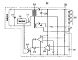
- the conventional LED lighting device 300 described in Patent Document 1 includes an LED driving device 201 and an LED 202.
- the LED driving device 201 includes an input capacitor 211, a transformer 212, a MOSFET 213, a controller 219, and an output capacitor 220. Further, the LED driving device 201 includes an error amplifier 215, a diode 216, and a photocoupler 217.
- the error amplifier 215 of the conventional LED lighting device 300 performs a calculation based on the voltage generated in the current detection resistor 218 and the voltage value of the reference voltage source, and feeds back the calculation result to the controller 219 via the photocoupler 217.
- the LED driving device 201 controls the current flowing through the LED 202 to be constant.
- the present invention provides an LED lighting circuit that can be handled safely by quickly reducing the output voltage when the input voltage from a commercial power source or the like is lost.
- an LED lighting circuit that converts an input voltage into a desired DC voltage and supplies the LED to an LED, the transformer having at least a primary winding and a secondary winding, a switching element, and a control A transformer, an output capacitor, an input voltage detector, and a discharger, wherein the transformer receives the input voltage at one end of the primary winding, and the direct current is applied to the LED through the secondary winding.
- a voltage is supplied, and the switching element is connected to the other end of the primary winding and performs a switching operation according to a control signal output from the controller, and the output capacitor is connected to both ends of the secondary winding.
- the input voltage detector detects the input voltage and outputs a discharge signal corresponding to the detected height of the input voltage to the discharger, and the discharger is connected to both ends of the output capacitor. Connected To discharge the charge stored in the output capacitor in response to the discharge signal output from the input voltage detector.
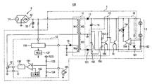
- FIG. 1 is a circuit diagram showing a configuration of an LED lighting circuit according to an embodiment of the present invention.
- the LED lighting circuit 1 according to the present embodiment includes a transformer 11 having at least a primary winding W1 and a secondary winding W2, a switching element 12, a controller 13, an output capacitor 14, an input voltage detector 15, And a discharger 16.
- the LED lighting circuit 1 includes an insulated power conversion circuit that converts an input voltage into a desired DC voltage and outputs the converted voltage.
- the LED 2 includes at least one LED element, and includes a series connection package and a parallel connection package including a plurality of LED elements, or a combination thereof.
- the input power source 3 is composed of a power source that outputs a DC input voltage, and may be composed of a DC power source such as a battery, or may be composed of a combination of an AC power source such as a commercial power source and a rectifying and smoothing circuit.
- the LED lighting circuit 1, LED 2, and input power source 3 are connected to each other, and the LED lighting circuit 1 and LED 2 constitute the LED lighting device 100 according to this embodiment.
- black dots added to the primary winding W1 and the secondary winding W2 of the transformer 11 indicate the polarity of the transformer.
- the primary winding W1 and the secondary winding W2 are wound in opposite polarities so that the secondary winding W2 becomes a flyback output winding.
- the primary winding W1 of the transformer 11 is connected to the input power supply 3, and the secondary winding W2 of the transformer 11 is connected to the LED2.
- the transformer 11 receives an input voltage from the input power source 3 at one end (positive side) of the primary winding W1, and supplies a DC voltage to the LED 2 connected to both ends of the secondary winding W2.
- the switching element 12 is composed of a MOSFET (Metal-Oxide-Semiconductor Field Effect Transistor).
- MOSFET Metal-Oxide-Semiconductor Field Effect Transistor
- the drain of the switching element 12 is connected to the other end (negative electrode side) of the primary winding W1 of the transformer 11, the source of the switching element 12 is connected to the primary side ground, and the gate of the switching element 12 is connected to the controller 13.
- the switching element 12 performs a switching operation (on / off operation) in accordance with a high-level or low-level control signal output from the controller 13, and conducts or cuts off a current flowing from the input power source 3 to the primary winding W1.
- An AC voltage is generated in the secondary winding W2 by the switching operation of the switching element 12.
- the output capacitor 14 is composed of an electrolytic capacitor or a ceramic capacitor, is connected to both ends of the secondary winding W2, and is equivalently connected in parallel to the LED2. One end of the output capacitor 14 is connected to one end (negative electrode side) of the secondary winding W2 via the diode 17, and the other end of the output capacitor 14 is connected to the other end (positive electrode side) of the secondary winding W2 and the secondary side ground. Connected to.
- the output capacitor 14 and the diode 17 constitute a rectifying / smoothing circuit, and convert an AC voltage generated in the secondary winding W2 to be supplied to the LED 2 into a DC voltage.
- the input voltage detector 15 is connected to the discharger 16, detects the input voltage output from the input power supply 3, and outputs a discharge signal corresponding to the level of the input voltage to the discharger 16.
- the input voltage detector 15 is configured to detect that at least the LED lighting circuit 1 is disconnected from the input power supply 3 and the input voltage is lost, and to allow the discharger 16 to perform a discharging operation when the input voltage is lost. .
- the discharger 16 is a well-known switch that can connect and disconnect between two terminals, and is connected to both ends of the output capacitor 14.
- the discharger 16 operates in response to the discharge signal output from the input voltage detector 15, and discharges the charge stored in the output capacitor 14 when the LED lighting circuit 1 is disconnected from the input power supply 3 and the input voltage is lost. To do.
- FIG. 2 is a circuit diagram showing a detailed configuration of the LED lighting circuit according to the embodiment of the present invention.
- the LED lighting circuit 1 according to the present embodiment further includes a feedback circuit 18 and an auxiliary power source 19.
- the LED 2 includes an LED string in which a plurality of LED elements are connected in series, and the input power source 3 includes a rectifying and smoothing circuit including a diode bridge 32 and a capacitor 33 and a commercial power source 31.
- the transformer 11 further includes a tertiary winding W3 and an auxiliary winding Wa, and one end (positive side) of the primary winding W1 is connected to one end of a capacitor 33 that is an output end of the rectifying and smoothing circuit.
- the tertiary winding W3 is a forward output winding different from the secondary winding W2, and the auxiliary winding is a flyback output winding.
- One end (negative electrode side) of the tertiary winding W3 is connected to the secondary side ground, and the other end (positive electrode side) is connected to the anode of the diode 151 of the input voltage detector 15.
- auxiliary winding Wa One end (negative electrode side) of the auxiliary winding Wa is connected to the controller 13 via a rectifying and smoothing circuit composed of a diode and a capacitor, and the other end (positive electrode side) is connected to the primary side ground.
- the auxiliary winding Wa and the rectifying / smoothing circuit constitute an auxiliary power source 19 that supplies driving power to the controller 13.
- the controller 13 is a PWM (Pulse Width Modulation) control system control circuit, and includes a PWM comparator 131, a triangular wave generator 132, voltage dividing resistors 133 and 134, a driver 135, a start circuit 136, and a regulator 137.
- the PWM comparator 131 compares a feedback signal described later and a triangular wave signal, and outputs a PWM signal for controlling the switching element 12 from the output terminal via the driver 135.
- the triangular wave generator 132 is connected to the inverting input terminal of the PWM comparator 131 and outputs a triangular wave signal.
- One end of the voltage dividing resistor 133 is connected to the regulator 137, the other end of the voltage dividing resistor 133 and one end of the voltage dividing resistor 134 are connected to each other, and the other end of the voltage dividing resistor 134 is connected to the primary side ground.
- the connection point of the voltage dividing resistors 133 and 134 is connected to the non-inverting input terminal of the PWM comparator 131 and the phototransistor 185 connected to the outside of the controller 13, and outputs a feedback signal corresponding to the current flowing through the LED 2.
- the start circuit 136 is connected to one end of the capacitor 33, the auxiliary power supply 19, and the regulator 137 through a resistor, and the regulator 137 supplies driving power to each part of the controller 13.
- the input voltage detector 15 in the LED lighting circuit 1 includes a diode 151, a capacitor 152, voltage dividing resistors 153 and 154, and a transistor 155.
- the anode of the diode 151 is connected to the other end of the tertiary winding W3, and the cathode is connected to one end of the capacitor 152 and the base of the transistor 155.
- the other end of the capacitor 152 is connected to the secondary side ground.
- the transistor 155 is an npn transistor.
- the collector of the transistor 155 is connected to one end of the output capacitor 14 via a resistor, and the emitter of the transistor 155 is connected to the secondary side ground.
- the charging voltage of the capacitor 152 is divided by the voltage dividing resistors 153 and 154 and applied to the base of the transistor 155.
- the tertiary winding W3 of the transformer 11 may be regarded as a part of the input voltage detector 15.
- the discharger 16 in the LED lighting circuit 1 is composed of an npn transistor, the collector of the discharger 16 is connected to one end of the output capacitor 14, and the emitter of the discharger 16 is connected to the secondary side ground.
- the base of electrical device 16 is connected to the collector of transistor 155. That is, the discharge signal of the input voltage detector 15 is output from the collector of the transistor 155 to the discharger 16.
- the feedback circuit 18 includes an error amplifier 181, a detection resistor 182, a Zener diode 183, a photodiode 184, and a phototransistor 185.
- the error amplifier 181 calculates an error between the current flowing through the LED 2 and the reference value and outputs the error to the photodiode 184.
- One end of the detection resistor 182 is connected in series with the LED 2 and connected to the inverting input terminal of the error amplifier 181, and the other end is connected to the secondary side ground.
- the detection resistor 182 outputs a voltage signal (detection signal) based on the current flowing through the LED 2.
- the anode of the Zener diode 183 is connected to the secondary side ground, and the cathode is connected to one end of the output capacitor 14 and the non-inverting input terminal of the error amplifier 181 through a resistor.
- the Zener diode 183 functions as a reference voltage source that outputs a reference value by clamping the voltage of the output capacitor 14.
- the anode of the photodiode 184 is connected to one end of the output capacitor 14, and the cathode is connected to the output terminal of the error amplifier 181.
- the collector of the phototransistor 185 is connected to the controller 13, and the emitter of the phototransistor 185 is connected to the primary side ground.
- the photodiode 184 and the phototransistor 185 constitute a photocoupler.
- the feedback circuit 18 outputs a feedback signal based on an error between the current flowing through the LED 2 and the reference value to the controller 13 via the photocoupler.
- a forward voltage based on the input voltage is generated in the tertiary winding W3 that is a forward output winding.
- the forward voltage is rectified and smoothed by the diode 151 and the capacitor 152 and converted to a DC signal corresponding to the level of the input voltage.
- a DC signal based on the input voltage is divided by voltage dividing resistors 153 and 154 and supplied to the base of the transistor 155. Therefore, a current flows between the collector and emitter of the transistor 155, and the discharger 16 is turned off.
- the level of the DC signal based on the forward voltage is lowered and the collector potential of the transistor 155 is increased. Turn on. Since the electric charge stored in the output capacitor 14 is rapidly discharged by the conduction of the discharger 16, the output voltage of the LED lighting circuit 1 immediately drops to near the base-emitter voltage (about 0.6V).
- the output capacitor 14 starts to be discharged under the following conditions.
- the voltage drop due to the diode bridge 32 is VF1
- the voltage drop due to the diode 151 is VF2
- the base emitter voltage drop due to the transistor 155 is VBE
- the resistance values of the voltage dividing resistors 153 and 154 are R1, R2, respectively.
- the number of turns of the primary winding W1 is nW1
- the number of turns of the tertiary winding W3 is nW3.
- the condition is that the effective value of the AC input voltage is (VF1 + (VF2 + VBE ⁇ (R1 + R2) / R2) ⁇ nW1 / nW3 or less).
- the instantaneous value of the AC input voltage is VF1 + VBE ⁇ (R1 + R2) / R2 ⁇ nW1 / nW3 or less.
- the LED lighting circuit it is possible to detect that the input voltage has become equal to or lower than a predetermined value and to rapidly discharge the charge stored in the output capacitor. Thereby, when the input voltage supplied from the input power source to the LED lighting device is lost in the operation of removing the LED lighting device or the like, it is possible to reduce the possibility of discharge to surrounding people or objects.
Landscapes
- Engineering & Computer Science (AREA)
- Power Engineering (AREA)
- Circuit Arrangement For Electric Light Sources In General (AREA)
- Led Devices (AREA)
- Dc-Dc Converters (AREA)
Abstract
本発明は、商用電源等からの入力電圧が無くなった場合に出力電圧をすみやかに降下させることで、安全に取り扱うことができるLED点灯回路を提供する。入力電圧を所望の直流電圧に変換してLEDに供給するLED点灯回路であって、少なくとも一次巻線および二次巻線を有するトランスと、スイッチング素子と、制御器と、出力コンデンサと、入力電圧検出器と、放電器と、を備え、前記入力電圧検出器は、前記入力電圧を検出し、検出された前記入力電圧の高さに応じた放電信号を前記放電器に出力し、前記放電器は、前記出力コンデンサの両端に接続され、前記入力電圧検出器から出力される前記放電信号に応じて前記出力コンデンサに蓄えられた電荷を放電する。
Description
本発明は、光源としてLED(Light Emitting Diode)を点灯させる絶縁型のLED点灯回路に関する。
LEDは、家庭用等の一般的な照明装置の光源にも近年利用されるようになり、直管型、環状型等の蛍光灯に対応する形態ばかりでなく、白熱電球に対応する電球型の照明装置が製造されるようになった。また、一般的に人が比較的容易に手を触れることができる用途の照明装置においては、感電防止等の安全性を備えることが要求されるため、LED点灯回路は、商用電源と負荷(LED)との間を電気的に絶縁するトランスを含んで構成される。
特許文献1には、上記のようにトランスを含む絶縁型のLED点灯回路が開示される。詳細には、図3に示すように、特許文献1に記載される従来のLED照明装置300は、LED駆動装置201とLED202とを有する。LED駆動装置201は、入力コンデンサ211と、トランス212と、MOSFET213と、制御器219と、出力コンデンサ220とを有する。また、LED駆動装置201は、誤差増幅器215と、ダイオード216と、フォトカプラ217とを有する。
従来のLED照明装置300の誤差増幅器215は、電流検出抵抗218に発生する電圧と基準電圧源の電圧値とに基づいて演算を行い、フォトカプラ217を介して制御器219に演算結果をフィードバックすることで、LED駆動装置201がLED202に流れる電流を一定に制御する。
ところで、従来のLED照明装置300を取り外すとき等、LED照明装置300が商用電源から切り離され入力電圧が無くなった場合、出力コンデンサ220に蓄えられた電荷が放電されにくく、出力電圧が0V付近まで降下せずLED202に触れた人や物に放電する可能性があった。このような可能性は、入力電圧がバッテリ等の直流電源から供給される場合においても同様である。
本発明は、商用電源等からの入力電圧が無くなった場合に出力電圧をすみやかに降下させることで、安全に取り扱うことができるLED点灯回路を提供するものである。
本発明の一態様によれば、入力電圧を所望の直流電圧に変換してLEDに供給するLED点灯回路であって、少なくとも一次巻線および二次巻線を有するトランスと、スイッチング素子と、制御器と、出力コンデンサと、入力電圧検出器と、放電器と、を備え、前記トランスは、前記一次巻線の一端に前記入力電圧を受け、前記二次巻線を介して前記LEDに前記直流電圧を供給し、前記スイッチング素子は、前記一次巻線の他端に接続され、前記制御器から出力される制御信号に応じてスイッチング動作し、前記出力コンデンサは、前記二次巻線の両端に接続され、前記入力電圧検出器は、前記入力電圧を検出し、検出された前記入力電圧の高さに応じた放電信号を前記放電器に出力し、前記放電器は、前記出力コンデンサの両端に接続され、前記入力電圧検出器から出力される前記放電信号に応じて前記出力コンデンサに蓄えられた電荷を放電する。
本発明によれば、商用電源等からの入力電圧が無くなった場合に出力電圧をすみやかに降下させることで、安全に取り扱うことができるLED点灯回路を提供することができる。
次に、図面を参照して、本発明の実施形態を説明する。以下の図面の記載において、同一又は類似の部分には同一又は類似の符号を付している。又、以下に示す実施形態は、この発明の技術的思想を具体化するための装置や方法を例示するものであって、この発明の技術的思想は、構成部品の形状、構造、配置等を下記のものに特定されるものでなく、この発明の実施形態は、種々の変更を加えることができる。
図1は、本発明の実施形態に係るLED点灯回路の構成を示す回路図である。本実施形態に係るLED点灯回路1は、少なくとも一次巻線W1および二次巻線W2を有するトランス11と、スイッチング素子12と、制御器13と、出力コンデンサ14と、入力電圧検出器15と、放電器16と、を備える。
LED点灯回路1は、入力電圧を所望の直流電圧に変換して出力する絶縁型の電力変換回路を含んで構成される。LED2は、少なくとも1つのLED素子を含んで構成され、複数のLED素子を含む直列接続パッケージおよび並列接続パッケージあるいはこれらの組合せにより構成される。入力電源3は、直流入力電圧を出力する電源からなり、バッテリ等の直流電源より構成されても良く、商用電源等の交流電源と整流平滑回路との組合せより構成されても良い。LED点灯回路1とLED2と入力電源3とは、それぞれ互いに接続され、LED点灯回路1とLED2とは、本実施形態に係るLED照明装置100を構成する。
図1においてトランス11の一次巻線W1および二次巻線W2に付記される黒点は、トランスの極性を示す。二次巻線W2がフライバック出力の巻線となるように、一次巻線W1と二次巻線W2とは互いに逆極性に巻き回される。トランス11の一次巻線W1は入力電源3に接続され、トランス11の二次巻線W2はLED2が接続される。トランス11は、一次巻線W1の一端(正極側)に入力電源3から入力電圧を受け、二次巻線W2の両端に接続されるLED2に直流電圧を供給する。
スイッチング素子12は、MOSFET(Metal-Oxide-Semiconductor Field Effect Transistor)からなる。スイッチング素子12のドレインは、トランス11の一次巻線W1の他端(負極側)に接続され、スイッチング素子12のソースは一次側接地に接続され、スイッチング素子12のゲートは制御器13に接続される。スイッチング素子12は、制御器13から出力されるハイレベルまたはローレベルの制御信号に応じてスイッチング動作(オンオフ動作)し、入力電源3から一次巻線W1に流れる電流を導通または遮断させる。スイッチング素子12のスイッチング動作により、交流電圧が二次巻線W2に発生する。
出力コンデンサ14は、電解コンデンサまたはセラミックコンデンサからなり、二次巻線W2の両端に接続され、LED2と等価的に並列接続される。出力コンデンサ14の一端はダイオード17を介して二次巻線W2の一端(負極側)に接続され、出力コンデンサ14の他端は二次巻線W2の他端(正極側)および二次側接地に接続される。出力コンデンサ14とダイオード17とは、整流平滑回路を構成し、LED2に供給するために二次巻線W2に発生する交流電圧を直流電圧に変換する。
入力電圧検出器15は、放電器16に接続され、入力電源3から出力される入力電圧を検出し、入力電圧の高低に応じた放電信号を放電器16に出力する。入力電圧検出器15は、少なくともLED点灯回路1が入力電源3から切り離され入力電圧が無くなったことを検出し、入力電圧が無くなったときに放電器16に放電動作をさせられるように構成される。
放電器16は、2つの端子間を導通および遮断させることができる周知の開閉器からなり、出力コンデンサ14の両端に接続される。放電器16は、入力電圧検出器15から出力される放電信号に応じて動作し、LED点灯回路1が入力電源3から切り離され入力電圧が無くなった場合に出力コンデンサ14に蓄えられた電荷を放電する。
図2は、本発明の実施形態に係るLED点灯回路の詳細な構成を示す回路図である。本実施形態に係るLED点灯回路1は、さらにフィードバック回路18と補助電源19とを備える。LED2は、複数のLED素子が直列接続されたLEDストリングからなり、入力電源3は、ダイオードブリッジ32およびコンデンサ33を含む整流平滑回路と商用電源31とからなる。
本実施形態において、トランス11はさらに三次巻線W3と補助巻線Waとを有し、一次巻線W1の一端(正極側)は、整流平滑回路の出力端であるコンデンサ33の一端に接続される。三次巻線W3は上記の二次巻線W2と異なるフォワード出力の巻線であり、補助巻線はフライバック出力の巻線である。三次巻線W3の一端(負極側)は二次側接地に接続され、他端(正極側)は入力電圧検出器15のダイオード151のアノードに接続される。補助巻線Waの一端(負極側)は、ダイオードとコンデンサとからなる整流平滑回路を介して制御器13に接続され、他端(正極側)は一次側接地に接続される。補助巻線Waと整流平滑回路とは、制御器13に駆動電力を供給する補助電源19を構成する。
本実施形態において、制御器13はPWM(Pulse Width Modulation)制御方式の制御回路であり、PWMコンパレータ131と三角波発生器132と分圧抵抗133、134とドライバ135とスタート回路136とレギュレータ137とを備える。PWMコンパレータ131は、後述するフィードバック信号と三角波信号とを比較して、出力端子からドライバ135を介してスイッチング素子12を制御するためのPWM信号を出力する。三角波発生器132は、PWMコンパレータ131の反転入力端子に接続され、三角波信号を出力する。分圧抵抗133の一端はレギュレータ137に接続され、分圧抵抗133の他端と分圧抵抗134の一端とは互いに接続され、分圧抵抗134の他端は一次側接地に接続される。分圧抵抗133、134の接続点は、PWMコンパレータ131の非反転入力端子と制御器13の外部に接続されるフォトトランジスタ185とに接続され、LED2に流れる電流に応じたフィードバック信号を出力する。スタート回路136は、抵抗を介してコンデンサ33の一端と補助電源19とレギュレータ137とに接続され、レギュレータ137は制御器13の各部に駆動電力を供給する。
本実施形態に係るLED点灯回路1における入力電圧検出器15は、ダイオード151とコンデンサ152と分圧抵抗153、154とトランジスタ155とを備える。ダイオード151のアノードは三次巻線W3の他端に接続され、カソードはコンデンサ152の一端とトランジスタ155のベースとに接続される。コンデンサ152の他端は二次側接地に接続される。トランジスタ155はnpnトランジスタからなり、トランジスタ155のコレクタは、抵抗を介して出力コンデンサ14の一端に接続され、トランジスタ155のエミッタは二次側接地に接される。また、トランジスタ155のベースには、コンデンサ152の充電電圧が分圧抵抗153、154で分圧されて印加される。なお、本実施形態において、トランス11の三次巻線W3を入力電圧検出器15の一部とみなしても良い。
本実施形態に係るLED点灯回路1における放電器16は、npnトランジスタからなり、放電器16のコレクタは出力コンデンサ14の一端に接続され、放電器16のエミッタは二次側接地に接続され、放電器16のベースはトランジスタ155のコレクタに接続される。すなわち、入力電圧検出器15の放電信号はトランジスタ155のコレクタから放電器16に出力される。
フィードバック回路18は、誤差増幅器181と検出抵抗182とツェナーダイオード183とフォトダイオード184とフォトトランジスタ185とを備える。誤差増幅器181はLED2に流れる電流と基準値との誤差を求め、フォトダイオード184に出力する。検出抵抗182の一端はLED2と直列に接続され、且つ誤差増幅器181の反転入力端子に接続され、他端は二次側接地に接続される。検出抵抗182は、LED2に流れる電流に基づく電圧信号(検出信号)を出力する。ツェナーダイオード183のアノードは二次側接地に接続され、カソードは抵抗を介して出力コンデンサ14の一端と誤差増幅器181の非反転入力端子とに接続される。ツェナーダイオード183は、出力コンデンサ14の電圧をクランプすることで基準値を出力する基準電圧源として機能する。フォトダイオード184のアノードは出力コンデンサ14の一端に接続され、カソードは誤差増幅器181の出力端子に接続される。フォトトランジスタ185のコレクタは制御器13に接続され、フォトトランジスタ185のエミッタは一次側接地に接続される。フォトダイオード184とフォトトランジスタ185とはフォトカプラを構成する。フィードバック回路18は、LED2に流れる電流と基準値との誤差に基づくフィードバック信号を、フォトカプラを介して制御器13に出力する。
本実施形態に係るLED点灯回路1における入力電圧検出器15および放電器16の動作について説明する。まず、入力電源3からLED点灯回路1に電力が供給される場合、フォワード出力巻線である三次巻線W3には入力電圧に基づくフォワード電圧が発生する。フォワード電圧は、ダイオード151およびコンデンサ152により整流平滑され、入力電圧の高低に応じた直流信号に変換される。入力電圧に基づく直流信号は、分圧抵抗153、154により分圧され、トランジスタ155のベースに供給される。そのため、トランジスタ155のコレクタ・エミッタ間には電流が流れ、放電器16はオフする。
次に、入力電源3からの入力電圧が無く、LED点灯回路1に電力が供給されない場合、フォワード電圧に基づく直流信号のレベルが低くなり、トランジスタ155のコレクタ電位が上昇するため、放電器16がオンする。出力コンデンサ14に蓄えられた電荷は、放電器16の導通により急速に放電されるため、LED点灯回路1の出力電圧はすみやかにベース・エミッタ電圧(約0.6V)付近まで降下する。
本実施形態に係るLED点灯回路1によれば、以下の条件で出力コンデンサ14が放電され始める。ただし、以下の式において、ダイオードブリッジ32による電圧降下をVF1、ダイオード151による電圧降下をVF2、トランジスタ155によるベース・エミッタ電圧降下をVBE、分圧抵抗153、154の抵抗値をそれぞれR1、R2、一次巻線W1の巻数をnW1、三次巻線W3の巻数をnW3とする。まず、入力コンデンサ14として容量が比較的大きい電解コンデンサ等を用いる場合、交流入力電圧の実効値が(VF1+(VF2+VBE×(R1+R2)/R2)×nW1/nW3以下であることが条件となる。次に、入力コンデンサ14として容量が比較的小さいフィルムコンデンサ等を用いる場合、交流入力電圧の瞬時値がVF1+VBE×(R1+R2)/R2×nW1/nW3以下であることが条件となる。
本実施形態に係るLED点灯回路によれば、入力電圧が所定値以下になったことを検出し、出力コンデンサに蓄えられた電荷を急速に放電することができる。これにより、LED照明装置の取り外し作業等において入力電源からLED照明装置に供給されていた入力電圧が無くなった場合に、周囲の人や物に放電してしまう可能性を低減することができる。
上記のように、本発明は実施形態によって記載したが、この開示の一部をなす論述及び図面はこの発明を限定するものであると理解すべきではない。この開示から当業者には様々な代替実施形態、実施例及び運用技術が明らかとなろう。即ち、本発明はここでは記載していない様々な実施形態等を含む。
本発明によれば、作業者が安全に取り扱うことができるLED点灯回路ならびにLED照明装置を提供することができる。
1 LED点灯回路
2 LED
3 入力電源
11 トランス
12 スイッチング素子
13 制御器
14 出力コンデンサ
15 入力電圧検出器
16 放電器
17 ダイオード
18 フィードバック回路
19 補助電源
2 LED
3 入力電源
11 トランス
12 スイッチング素子
13 制御器
14 出力コンデンサ
15 入力電圧検出器
16 放電器
17 ダイオード
18 フィードバック回路
19 補助電源
Claims (4)
- 入力電圧を所望の直流電圧に変換してLEDに供給するLED点灯回路であって、
少なくとも一次巻線および二次巻線を有するトランスと、スイッチング素子と、制御器と、出力コンデンサと、入力電圧検出器と、放電器と、を備え、
前記トランスは、前記一次巻線の一端に前記入力電圧を受け、前記二次巻線を介して前記LEDに前記直流電圧を供給し、
前記スイッチング素子は、前記一次巻線の他端に接続され、前記制御器から出力される制御信号に応じてスイッチング動作し、
前記出力コンデンサは、前記二次巻線の両端に接続され、
前記入力電圧検出器は、前記入力電圧を検出し、検出された前記入力電圧の高さに応じた放電信号を前記放電器に出力し、
前記放電器は、前記出力コンデンサの両端に接続され、前記入力電圧検出器から出力される前記放電信号に応じて前記出力コンデンサに蓄えられた電荷を放電するLED点灯回路。 - 前記トランスは少なくとも三次巻線を有し、前記三次巻線はフォワード出力巻線であり、前記入力電圧検出器は前記三次巻線を介して前記入力電圧を検出する請求項1に記載のLED点灯回路。
- 前記入力電圧検出器は、前記入力電圧が所定値以下になったことを検出し、前記放電器を動作させ、前記出力コンデンサに蓄えられた電荷を放電させる請求項1または2に記載のLED点灯回路。
- 前記二次巻線はフライバック出力巻線である請求項1乃至3のいずれか1項に記載のLED点灯回路。
Applications Claiming Priority (2)
| Application Number | Priority Date | Filing Date | Title |
|---|---|---|---|
| JP2011-205201 | 2011-09-20 | ||
| JP2011205201A JP2013069426A (ja) | 2011-09-20 | 2011-09-20 | Led点灯回路 |
Publications (1)
| Publication Number | Publication Date |
|---|---|
| WO2013042673A1 true WO2013042673A1 (ja) | 2013-03-28 |
Family
ID=47914436
Family Applications (1)
| Application Number | Title | Priority Date | Filing Date |
|---|---|---|---|
| PCT/JP2012/073879 Ceased WO2013042673A1 (ja) | 2011-09-20 | 2012-09-19 | Led点灯回路 |
Country Status (2)
| Country | Link |
|---|---|
| JP (1) | JP2013069426A (ja) |
| WO (1) | WO2013042673A1 (ja) |
Cited By (1)
| Publication number | Priority date | Publication date | Assignee | Title |
|---|---|---|---|---|
| CN112986787A (zh) * | 2021-05-20 | 2021-06-18 | 江西省兆驰光电有限公司 | 一种发光二极管测试装置 |
Citations (4)
| Publication number | Priority date | Publication date | Assignee | Title |
|---|---|---|---|---|
| JP2005019266A (ja) * | 2003-06-27 | 2005-01-20 | Tabuchi Electric Co Ltd | 高調波電流抑制回路を備えた放電ランプ用電源回路 |
| JP2009296790A (ja) * | 2008-06-05 | 2009-12-17 | Sharp Corp | スイッチング電源装置 |
| JP2010055824A (ja) * | 2008-08-26 | 2010-03-11 | Panasonic Electric Works Co Ltd | Led駆動装置、照明装置及び照明器具 |
| JP2010153599A (ja) * | 2008-12-25 | 2010-07-08 | Funai Electric Co Ltd | 電源回路およびそれを備えた電子機器 |
-
2011
- 2011-09-20 JP JP2011205201A patent/JP2013069426A/ja active Pending
-
2012
- 2012-09-19 WO PCT/JP2012/073879 patent/WO2013042673A1/ja not_active Ceased
Patent Citations (4)
| Publication number | Priority date | Publication date | Assignee | Title |
|---|---|---|---|---|
| JP2005019266A (ja) * | 2003-06-27 | 2005-01-20 | Tabuchi Electric Co Ltd | 高調波電流抑制回路を備えた放電ランプ用電源回路 |
| JP2009296790A (ja) * | 2008-06-05 | 2009-12-17 | Sharp Corp | スイッチング電源装置 |
| JP2010055824A (ja) * | 2008-08-26 | 2010-03-11 | Panasonic Electric Works Co Ltd | Led駆動装置、照明装置及び照明器具 |
| JP2010153599A (ja) * | 2008-12-25 | 2010-07-08 | Funai Electric Co Ltd | 電源回路およびそれを備えた電子機器 |
Cited By (2)
| Publication number | Priority date | Publication date | Assignee | Title |
|---|---|---|---|---|
| CN112986787A (zh) * | 2021-05-20 | 2021-06-18 | 江西省兆驰光电有限公司 | 一种发光二极管测试装置 |
| CN112986787B (zh) * | 2021-05-20 | 2021-07-30 | 江西省兆驰光电有限公司 | 一种发光二极管测试装置 |
Also Published As
| Publication number | Publication date |
|---|---|
| JP2013069426A (ja) | 2013-04-18 |
Similar Documents
| Publication | Publication Date | Title |
|---|---|---|
| US8310169B2 (en) | Power conversion driving circuit and fluorescent lamp driving circuit | |
| CN104145529B (zh) | Led光源和减少通过led光源的led负载的漏电流的方法 | |
| CN107637169B (zh) | 可延时照明电路及装置 | |
| TWI481140B (zh) | Switching power supply circuit and electronic equipment with protection function | |
| CN103038992B (zh) | 带保护功能的开关电源电路 | |
| JP2012216766A (ja) | Led駆動装置及びled照明装置 | |
| JP5732072B2 (ja) | Led照明 | |
| JP6087937B2 (ja) | Ledを電子バラストに接続するためのドライバ | |
| JP5595255B2 (ja) | Led電源装置 | |
| JP6136173B2 (ja) | 直流電源装置 | |
| US9306387B2 (en) | Current limiting circuit and method for LED driver | |
| JP4968399B2 (ja) | Led駆動装置及びled照明装置 | |
| JP2015053225A (ja) | Led駆動回路 | |
| KR101365307B1 (ko) | 발광다이오드 조명 기기를 위한 스위칭 전원 공급 장치 회로 | |
| US10334673B2 (en) | Lighting system | |
| JP2006352975A (ja) | スイッチング電源装置 | |
| WO2013042673A1 (ja) | Led点灯回路 | |
| US9265120B2 (en) | Lighting device and luminaire using same | |
| KR101568855B1 (ko) | Led 컨버터 lc 피드백 안정화 회로 | |
| JP6405863B2 (ja) | 照明装置 | |
| JP7327123B2 (ja) | 点灯装置および照明装置 | |
| CN110351920B (zh) | 驱动器和照明模块 | |
| JP5842129B2 (ja) | Led点灯装置及びそれを用いた照明器具 | |
| JP7027964B2 (ja) | 点灯装置、照明器具および照明システム | |
| CN114641109B (zh) | 一种多模式调光电路及灯具 |
Legal Events
| Date | Code | Title | Description |
|---|---|---|---|
| 121 | Ep: the epo has been informed by wipo that ep was designated in this application |
Ref document number: 12834278 Country of ref document: EP Kind code of ref document: A1 |
|
| NENP | Non-entry into the national phase |
Ref country code: DE |
|
| 122 | Ep: pct application non-entry in european phase |
Ref document number: 12834278 Country of ref document: EP Kind code of ref document: A1 |