WO2013031943A1 - 照明方法及び発光装置 - Google Patents
照明方法及び発光装置 Download PDFInfo
- Publication number
- WO2013031943A1 WO2013031943A1 PCT/JP2012/072144 JP2012072144W WO2013031943A1 WO 2013031943 A1 WO2013031943 A1 WO 2013031943A1 JP 2012072144 W JP2012072144 W JP 2012072144W WO 2013031943 A1 WO2013031943 A1 WO 2013031943A1
- Authority
- WO
- WIPO (PCT)
- Prior art keywords
- light
- emitting device
- light emitting
- ssl
- ref
- Prior art date
Links
Images


Classifications
-
- C—CHEMISTRY; METALLURGY
- C09—DYES; PAINTS; POLISHES; NATURAL RESINS; ADHESIVES; COMPOSITIONS NOT OTHERWISE PROVIDED FOR; APPLICATIONS OF MATERIALS NOT OTHERWISE PROVIDED FOR
- C09K—MATERIALS FOR MISCELLANEOUS APPLICATIONS, NOT PROVIDED FOR ELSEWHERE
- C09K11/00—Luminescent, e.g. electroluminescent, chemiluminescent materials
- C09K11/08—Luminescent, e.g. electroluminescent, chemiluminescent materials containing inorganic luminescent materials
-
- H—ELECTRICITY
- H01—ELECTRIC ELEMENTS
- H01L—SEMICONDUCTOR DEVICES NOT COVERED BY CLASS H10
- H01L33/00—Semiconductor devices with at least one potential-jump barrier or surface barrier specially adapted for light emission; Processes or apparatus specially adapted for the manufacture or treatment thereof or of parts thereof; Details thereof
- H01L33/02—Semiconductor devices with at least one potential-jump barrier or surface barrier specially adapted for light emission; Processes or apparatus specially adapted for the manufacture or treatment thereof or of parts thereof; Details thereof characterised by the semiconductor bodies
- H01L33/26—Materials of the light emitting region
- H01L33/30—Materials of the light emitting region containing only elements of group III and group V of the periodic system
- H01L33/32—Materials of the light emitting region containing only elements of group III and group V of the periodic system containing nitrogen
-
- H—ELECTRICITY
- H01—ELECTRIC ELEMENTS
- H01L—SEMICONDUCTOR DEVICES NOT COVERED BY CLASS H10
- H01L33/00—Semiconductor devices with at least one potential-jump barrier or surface barrier specially adapted for light emission; Processes or apparatus specially adapted for the manufacture or treatment thereof or of parts thereof; Details thereof
- H01L33/48—Semiconductor devices with at least one potential-jump barrier or surface barrier specially adapted for light emission; Processes or apparatus specially adapted for the manufacture or treatment thereof or of parts thereof; Details thereof characterised by the semiconductor body packages
- H01L33/50—Wavelength conversion elements
- H01L33/501—Wavelength conversion elements characterised by the materials, e.g. binder
- H01L33/502—Wavelength conversion materials
- H01L33/504—Elements with two or more wavelength conversion materials
-
- H—ELECTRICITY
- H05—ELECTRIC TECHNIQUES NOT OTHERWISE PROVIDED FOR
- H05B—ELECTRIC HEATING; ELECTRIC LIGHT SOURCES NOT OTHERWISE PROVIDED FOR; CIRCUIT ARRANGEMENTS FOR ELECTRIC LIGHT SOURCES, IN GENERAL
- H05B45/00—Circuit arrangements for operating light-emitting diodes [LED]
- H05B45/20—Controlling the colour of the light
- H05B45/22—Controlling the colour of the light using optical feedback
-
- H—ELECTRICITY
- H05—ELECTRIC TECHNIQUES NOT OTHERWISE PROVIDED FOR
- H05B—ELECTRIC HEATING; ELECTRIC LIGHT SOURCES NOT OTHERWISE PROVIDED FOR; CIRCUIT ARRANGEMENTS FOR ELECTRIC LIGHT SOURCES, IN GENERAL
- H05B45/00—Circuit arrangements for operating light-emitting diodes [LED]
- H05B45/20—Controlling the colour of the light
- H05B45/24—Controlling the colour of the light using electrical feedback from LEDs or from LED modules
-
- H—ELECTRICITY
- H01—ELECTRIC ELEMENTS
- H01L—SEMICONDUCTOR DEVICES NOT COVERED BY CLASS H10
- H01L2924/00—Indexing scheme for arrangements or methods for connecting or disconnecting semiconductor or solid-state bodies as covered by H01L24/00
- H01L2924/0001—Technical content checked by a classifier
- H01L2924/0002—Not covered by any one of groups H01L24/00, H01L24/00 and H01L2224/00
-
- H—ELECTRICITY
- H01—ELECTRIC ELEMENTS
- H01L—SEMICONDUCTOR DEVICES NOT COVERED BY CLASS H10
- H01L33/00—Semiconductor devices with at least one potential-jump barrier or surface barrier specially adapted for light emission; Processes or apparatus specially adapted for the manufacture or treatment thereof or of parts thereof; Details thereof
- H01L33/48—Semiconductor devices with at least one potential-jump barrier or surface barrier specially adapted for light emission; Processes or apparatus specially adapted for the manufacture or treatment thereof or of parts thereof; Details thereof characterised by the semiconductor body packages
- H01L33/50—Wavelength conversion elements
- H01L33/501—Wavelength conversion elements characterised by the materials, e.g. binder
- H01L33/502—Wavelength conversion materials
Definitions
- the present invention relates to an illumination method in which light emitted from a light-emitting device including a semiconductor light-emitting element that is a light-emitting element illuminates an object, and a light-emitting device that includes a semiconductor light-emitting element that is a light-emitting element.
- a GaN-based blue light-emitting element is included as an excitation light source of a yellow phosphor, and a so-called pseudo-white light source is created from the spectrum of the GaN-based blue light-emitting element and the spectrum of the yellow phosphor, or an illumination light source, or It is widely practiced to use a lighting fixture that includes this, and a lighting system in which a plurality of such fixtures are arranged in a space. (See Patent Document 1)
- a packaged LED for example, the package material includes the GaN-based blue light emitting element, yellow phosphor, sealant, etc.
- the package material includes the GaN-based blue light emitting element, yellow phosphor, sealant, etc.
- the package material includes the GaN-based blue light emitting element, yellow phosphor, sealant, etc.
- the temperature (Correlated Color Temperature / CCT) region there is a product whose light source efficiency as a package LED exceeds 150 lm / W. (See Non-Patent Document 2) Further, the efficiency and power saving of the light source for liquid crystal backlights is also progressing.
- Non-Patent Document 1 describes an illumination light source having a red color tone.
- the color rendering index is the color when illuminated with the test light against the appearance of the color illuminated with the “reference light” selected corresponding to the CCT of the light (test light) of the light emitting device to be evaluated. It is an index showing how close the appearance of the is. That is, the color rendering index is an index indicating the fidelity of the light emitting device to be evaluated.
- the average color rendering index (R a ) or special color rendering index (R i (i is 1 to 14, i is 1 to 15 according to JIS regulations in Japan)) is high. It is becoming clear that it does not induce good color perception. That is, there is a problem that these methods for improving the score of the color rendering evaluation number do not always realize a good color appearance.
- the effect of changing the color appearance depending on the illuminance of the object to be illuminated is not included in various current color rendering evaluation indices (color rendition metrics).
- color rendering evaluation indices color rendition metrics.
- the degree of saturation related to the appearance of the color of an object depends on the illuminance, and the degree of saturation decreases as the illuminance decreases even if the illuminated spectral distribution is the same. That is, the color appearance is dull. This is known as the Hunt effect.
- the hunt effect greatly affects the color rendering, it is not actively considered in the evaluation of light emitting devices such as current light sources, fixtures, and systems.
- the simplest compensation method for the hunt effect is to extremely increase the room illuminance, but this unnecessarily increases the energy consumption.
- the present invention has been made in order to solve the above-described problems, and includes an indoor illumination environment that is about 5000 lx or less, or generally about 1500 lx or less, including the case where fine work is performed.
- the color appearance perceived by humans is natural, lively, and highly visible, as seen in an outdoor high-light environment, regardless of the scores of various color rendering metrics (color rendition metrics).
- an object of the present invention is to realize a comfortable lighting environment with high efficiency.
- It is another object of the present invention to provide design guidelines for such a preferred light emitting device.
- An illumination method including an illumination object preparation step of preparing an illumination object, and an illumination step of illuminating the object with light emitted from a light emitting device including a semiconductor light emitting element that is a light emitting element,
- illumination is performed so that the light measured at the position of the object satisfies the following (1), (2), and (3)
- a lighting method characterized by: (1) Distance D from the black body radiation locus defined by ANSI C78.377 of the light measured at the position of the object. UVSSL -0.0350 ⁇ D uvSSL ⁇ 0.0040.
- the illumination method according to [1] The spectral distribution of light measured at the position of the object is ⁇ SSL ( ⁇ ), T of light measured at the position of the object SSL
- the spectral distribution of the reference light selected according to (K) is ⁇ ref ( ⁇ ), the tristimulus value of light measured at the position of the object (X SSL , Y SSL , Z SSL ) T of light measured at the position of the object SSL
- the lighting method characterized by being.
- the semiconductor light emitting element is on any substrate selected from the group consisting of a sapphire substrate, a GaN substrate, a GaAs substrate, and a GaP substrate.
- Lighting method characterized by being created in [22] The illumination method according to any one of [1] to [20], wherein the semiconductor light emitting element is formed on a GaN substrate or a GaP substrate, and the thickness of the substrate is not less than 100 ⁇ m and not more than 2 mm.
- c, d and x are 2.7 ⁇ c ⁇ 3.3, 0.9 ⁇ d ⁇ 1.1, 0.3 ⁇ x ⁇ .
- An illumination method comprising a phosphor having a wavelength of 2 nm to 130 nm.
- Kx trivalent rare earth element
- k, x, and y represent numbers satisfying 2.8 ⁇ k ⁇ 5, 0.1 ⁇ x ⁇ 0.7, and 0.005 ⁇ y ⁇ 0.015, respectively.
- A is calcium (Ca), strontium (Sr), barium (Ba), zinc (Zn), or a mixture thereof.
- the lighting method characterized by being.
- the illumination method according to any one of [1] to [34] which is used for production.
- the illumination method according to any one of [1] to [34] which is used for medical purposes.
- a light-emitting device comprising at least a semiconductor light-emitting element as a light-emitting element, The light emitted from the light emitting device is a distance D from the black body radiation locus defined by ANSI C78.377.
- the spectral distribution of light emitted from the light emitting device in the radiation direction is ⁇ SSL ( ⁇ ), T of light emitted from the light emitting device in the radiation direction SSL
- the spectral distribution of the reference light selected according to (K) is ⁇ ref ( ⁇ ), the tristimulus value of light emitted in the radiation direction from the light emitting device (X SSL , Y SSL , Z SSL ) T of light emitted from the light emitting device in the radiation direction SSL
- the reference light tristimulus values selected according to (K) are expressed as (X ref , Y ref , Z ref )age, Standardized spectral distribution S of light emitted from the light emitting device in the radiation direction SSL ( ⁇ ) and T of light emitted from the light emitting device in the radiation direction SSL Normalized spectral distribution S of the reference light selected according to (K) ref ( ⁇ ) and the difference ⁇ S
- a light emitting device including at least a semiconductor light emitting element as a light emitting element,
- the light emitted from the light emitting device is a distance D from the black body radiation locus defined by ANSI C78.377.
- the spectral distribution of light emitted from the light emitting device in the radiation direction is ⁇ SSL ( ⁇ ), T of light emitted from the light emitting device in the radiation direction SSL
- the spectral distribution of the reference light selected according to (K) is ⁇ ref ( ⁇ ), the tristimulus value of light emitted in the radiation direction from the light emitting device (X SSL , Y SSL , Z SSL ) T of light emitted from the light emitting device in the radiation direction SSL
- the reference light tristimulus values selected according to (K) are expressed as (X ref , Y ref , Z ref )age, Standardized spectral distribution S
- the light-emitting device according to any one of [44] to [56], wherein the light-emitting device is emitted from one to six types of light-emitting elements including light emitted from the semiconductor light-emitting element.
- a light emitting device that emits light in the radiation direction.
- the peak wavelength of the emission spectrum of the semiconductor light-emitting element is 380 nm or more and less than 495 nm, and the full width at half maximum is 2 nm or more and 45 nm or less.
- the light-emitting device according to any one of [44] to [63], wherein the semiconductor light-emitting element is on any substrate selected from the group consisting of a sapphire substrate, a GaN substrate, a GaAs substrate, and a GaP substrate.
- the light-emitting device according to any one of [44] to [63], wherein the semiconductor light-emitting element is formed on a GaN substrate or a GaP substrate, and the thickness of the substrate is not less than 100 ⁇ m and not more than 2 mm.
- [66] The light emitting device according to any one of [44] to [63], wherein the semiconductor light emitting element is formed on a sapphire substrate or a GaAs substrate, and the semiconductor light emitting element is peeled off from the substrate.
- the phosphor includes one to five types of phosphors having different emission spectra.
- a light emitting device comprising a phosphor having a thickness of 2 nm to 90 nm.
- c, d and x are 2.7 ⁇ c ⁇ 3.3, 0.9 ⁇ d ⁇ 1.1, 0.3 ⁇ x ⁇ .
- a light-emitting device including a phosphor with a thickness of 2 nm to 130 nm.
- the phosphor is represented by the following general formula (7), the phosphor represented by the following general formula (7) ', (Sr, Ca , Ba) 2 Al x Si 5-x O x N 8-x : Eu (where 0 ⁇ x ⁇ 2), Eu y (Sr, Ca, Ba) 1-y : Al 1 + x Si 4-x O x N 7-x (Where 0 ⁇ x ⁇ 4, 0 ⁇ y ⁇ 0.2), K 2 SiF 6 : Mn 4+ , A 2 + x M y Mn z F n (A is Na and / or K; M is Si and Al; ⁇ 1 ⁇ x ⁇ 1 and 0.9 ⁇ y + z ⁇ 1.1 and 0.001 ⁇ z ⁇ 0.4 and 5 ⁇ n ⁇ 7), Ca,
- A is calcium (Ca), strontium (Sr), barium (Ba), zinc (Zn), or a mixture thereof.
- the light-emitting device according to any one of [44] to [57], comprising a phosphor as a light-emitting element, wherein the semiconductor light-emitting element has an emission spectrum peak wavelength of 395 nm or more and less than 420 nm,
- the light emitting device characterized in that the body includes SCA, ⁇ -SiAlON, and CASON.
- the light-emitting device according to any one of [44] to [76], which is any one selected from the group consisting of a packaged LED, an LED module, an LED lighting fixture, and an LED lighting system.
- the light emitting device according to any one of [44] to [77], which is used as a home lighting device.
- the third embodiment of the present invention for achieving the above object relates to the following matters.
- the spectral distribution of light emitted from the light emitting device in the radiation direction is ⁇ SSL ( ⁇ ), T of light emitted from the light emitting device in the radiation direction SSL
- the spectral distribution of the reference light selected according to (K) is ⁇ ref ( ⁇ ), the tristimulus value of light emitted in the radiation direction from the light emitting device (X SSL , Y SSL , Z SSL ) T of light emitted from the light emitting device in the radiation direction SSL
- the reference light tristimulus values selected according to (K) are expressed as (X ref , Y ref , Z ref )age, Standardized spectral distribution S of light emitted from the light emitting device in the radiation direction SSL ( ⁇ ) and T of light emitted from the light emitting device in the radiation direction SSL Normalized spectral distribution S of the reference light selected according to (K) ref ( ⁇ ) and
- a method for designing a light-emitting device including at least a semiconductor light-emitting element as a light-emitting element is the light emitted from the light emitting device.
- the spectral distribution of light emitted from the light emitting device in the radiation direction is ⁇ SSL ( ⁇ ), T of light emitted from the light emitting device in the radiation direction SSL
- the spectral distribution of the reference light selected according to (K) is ⁇ ref ( ⁇ ), the tristimulus value of light emitted in the radiation direction from the light emitting device (X SSL , Y SSL , Z SSL ) T of light emitted from the light emitting device in the radiation direction SSL
- the reference light tristimulus values selected according to (K) are expressed as (X ref , Y ref , Z ref )age, Standardized spectral distribution S of light emitted from the light emitting device in the radiation direction SSL ( ⁇ ) and T of light emitted from the light emitting device in the radiation direction SSL Normalized spectral distribution S of the reference light selected according to (K) ref ( ⁇ ) and
- the present invention when illuminated with (if there is described a laboratory reference light) reference light and a high R a and high R i becomes color appearance close to the light of the reference light Compared to the case of illuminating with a light emitting device that emits (which may be described as a pseudo-reference light for experiments), even if the CCT and the illuminance are almost the same, a large number of subjects are statistically more An illumination method and a light-emitting device capable of realizing a truly good color appearance of an object that is determined to be good are realized.
- the effects realized by the present invention are as follows. First, when illuminated by the illumination method of the present invention, or when illuminated by a light-emitting device such as a light source, instrument, or system according to the present invention, when illuminated with experimental reference light or experimental simulated reference light, etc. In contrast, even with almost the same CCT and almost the same illuminance, white is whiter and looks natural and comfortable. Furthermore, it becomes easy to visually recognize the brightness difference between achromatic colors such as white, gray, and black. For this reason, for example, black characters on general white paper are easy to read. Although details will be described later, such an effect is completely unexpected in light of conventional common sense.
- the illuminance when illuminated by the illumination method of the present invention, or the illuminance realized by the light emitting device according to the present invention is purple even if it is about a normal indoor environment of several thousand Lx to several hundred Lx. , Violet, blue, blue-green, green, yellow-green, yellow, yellow-red, red, red-purple, etc. A truly natural color appearance as seen below about lx is achieved.
- the skin color of subjects Japanese people
- various foods, clothing, wood colors, and the like which have intermediate saturation, have natural colors that many subjects feel more preferable.
- the illumination method of the present invention illuminates even with substantially the same CCT and substantially the same illuminance, or When illuminated with a light source, instrument, or system according to the present invention, the object can be more clearly and easily seen as if viewed in a high illumination environment.
- a semiconductor light emitting device having a peak wavelength of 475 nm is incorporated, and is emitted from a package LED including a green phosphor and a red phosphor.
- a spectral distribution is assumed to illuminate 15 kinds of modified Munsell color charts, and is illuminated by the LED.
- a spectral distribution assuming that a semiconductor light emitting element having a peak wavelength of 405 nm is embedded, emitted from a package LED including a blue phosphor, a green phosphor, and a red phosphor and illuminated 15 kinds of modified Munsell color charts, and the LED
- FIG. 3 is a diagram illustrating a normalized test light spectral distribution (solid line) of the test light 5 and a normalized reference light spectral distribution (dotted line) of the calculation reference light corresponding to the test light 5;
- FIG. 6 is a diagram illustrating a CIELAB color space in which are plotted together.
- FIG. 3 is a diagram illustrating a normalized test light spectral distribution (solid line) of the test light 15 and a normalized reference light spectral distribution (dotted line) of the calculation reference light corresponding to the test light 15.
- FIG. 6 is a diagram illustrating a CIELAB color space in which are plotted together.
- FIG. 3 is a diagram illustrating a normalized test light spectral distribution (solid line) of the test light 19 and a normalized reference light spectral distribution (dotted line) of the calculation reference light corresponding to the test light 19;
- FIG. 6 is a diagram illustrating a CIELAB color space in which are plotted together.
- FIG. 4 is a diagram showing a normalized test light spectral distribution (solid line) of the comparative test light 14 and a normalized reference light spectral distribution (dotted line) of the calculation reference light corresponding to the comparative test light 14.
- the a * value and b of the fifteen kinds of corrected Munsell color charts assuming that the object is illuminated with the comparative test light 14 (solid line) and the case where the object is illuminated with the reference light for calculation corresponding to the comparative test light 14, respectively.
- the illumination method according to the first embodiment of the present invention is an invention in which light emitted from a light emitting device used in the illumination method illuminates the object, using light at a position where the object is illuminated. Is specified. Therefore, an illumination method using a light emitting device that can emit light at a “position where an object is illuminated” that satisfies the requirements of the present invention belongs to the scope of the present invention.
- the invention is specified by the light in the “main radiation direction” among the light emitted by the light emitting device. Therefore, a light-emitting device capable of emitting radiation including “main radiation direction” that satisfies the requirements of the present invention belongs to the scope of the present invention.
- the “main radiant direction” in the second and third embodiments of the present invention has a suitable range in accordance with the use state of the light emitting device, and a suitable orientation. Indicates the direction in which light is emitted. For example, it may be a direction in which the luminous intensity or luminance of the light emitting device is maximized or maximized. Further, the light emitting device may have a finite range including a direction in which the luminous intensity or luminance of the light emitting device is maximized or maximized. In addition, the radiant intensity or radiance of the light emitting device may be in the maximum or maximum direction.
- the light emitting device is a single light emitting diode (LED), a single package LED, a single LED module, a single LED bulb, a single composite lamp of a fluorescent lamp and a semiconductor light emitting element, a single composite lamp of an incandescent bulb and a semiconductor light emitting element, etc.
- the main radiation direction may be the vertical direction of each light emitting device and a finite solid angle including the vertical direction, for example, ⁇ (sr) at the maximum and ⁇ / 100 (sr) at the minimum.
- the light emitting device is an LED lighting device in which a lens, a reflection mechanism or the like is added to the packaged LED or the like, a lighting device including a fluorescent lamp and a semiconductor light emitting element, so-called direct type lighting application, semi-direct type lighting application, general diffusion
- the main radiation direction is a finite including the vertical direction and vertical direction of each light emitting device For example, ⁇ (sr) at the maximum and ⁇ / 100 (sr) at the minimum.
- the luminous intensity or luminance of the light emitting device may be in a direction that is maximized or maximized.
- the radiant intensity or radiance of the light emitting device may be in a direction that maximizes or maximizes.
- it may be within a finite solid angle including a direction in which the radiant intensity or radiance of the light emitting device is maximized or maximized, for example, ⁇ (sr) at the maximum and ⁇ / 100 (sr) at the minimum.
- the main radiation direction is a vertical direction of the planar center of each light-emitting device and a finite number including the vertical direction. It can be within a solid angle, for example, ⁇ (sr) at the maximum and ⁇ / 100 (sr) at the minimum.
- the luminous intensity or luminance of the light emitting device may be in a direction that is maximized or maximized. Further, it may be within a finite solid angle including the direction in which the luminous intensity or luminance of the light emitting device is maximized or maximized, for example, ⁇ (sr) at the maximum and ⁇ / 100 (sr) at the minimum.
- the radiant intensity or radiance of the light emitting device may be in a direction that maximizes or maximizes. Further, it may be within a finite solid angle including a direction in which the radiant intensity or radiance of the light emitting device is maximized or maximized, for example, ⁇ (sr) at the maximum and ⁇ / 100 (sr) at the minimum.
- ⁇ (sr) at the maximum
- ⁇ / 100 (sr) at the minimum.
- it is preferable to measure at a distance at which the illuminance at the measurement point becomes practical illuminance 150 lx to 5000 lx as described later).
- the reference light defined by the CIE used for calculation when predicting the appearance of mathematical colors is sometimes referred to as reference light, calculation reference light, calculation reference light, or the like.
- the experimental reference light used in the actual visual comparison that is, the incandescent bulb light in which the tungsten filament is contained, may be described as the reference light, the experimental reference light, and the experimental reference light.
- light having a high Ra and high Ri which is expected to have a color appearance close to the reference light, for example, an LED light source, which is used as a substitute light for the experimental reference light in the comparative visual experiment, Sometimes referred to as reference light, experimental pseudo-reference light, and experimental pseudo-reference light.
- the light that is mathematically and experimentally studied may be described as test light with respect to the reference light.
- the light-emitting device used in the illumination method according to the first embodiment of the present invention includes a semiconductor light-emitting element that is a light-emitting element.
- the light-emitting device according to the second embodiment of the present invention includes a semiconductor light-emitting element that is a light-emitting element.
- the other configurations are not particularly limited, and may be a single semiconductor light emitting element provided with a lead wire or the like as an energization mechanism, or a packaged LED that is further provided with a heat dissipation mechanism or the like and integrated with a phosphor or the like.
- an LED module in which a more robust heat dissipation mechanism is provided to one or more packaged LEDs and a plurality of packaged LEDs are mounted may be used.
- the LED lighting fixture which provided the lens, the light reflection mechanism, etc. to package LED etc. may be sufficient.
- the lighting system which supported many LED lighting fixtures etc. and was able to illuminate a target object may be sufficient.
- the light emitting device according to this embodiment includes all of them.
- the present inventor has a natural, lively, highly visible, comfortable, color appearance, and object appearance as seen in an outdoor high illumination environment even in a general indoor illumination environment.
- radiometric properties and photometric properties common to spectra or spectral distributions that can realize the above.
- how the color chart's color appearance having specific spectral reflection characteristics when illumination with light having the spectrum or spectral distribution is assumed is compared to when illumination with calculation reference light is assumed. From the viewpoint of colorimetry, whether the object can be realized when it changes (or when it does not change) has arrived at the present invention as a whole.
- the present invention has also been made based on experimental facts that overturn common sense. The outline until the specific invention was achieved was as follows.
- A) a package LED light source that has a high degree of freedom in setting a spectral distribution A) a package LED light source that includes both a semiconductor light emitting element and a phosphor, and B) a package LED that does not include a phosphor and includes only a semiconductor light emitting element
- a basic mathematical study was conducted.
- a guideline is provided for mathematical changes in the color appearance of the color chart having a specific spectral reflection characteristic between the case of assuming illumination with the reference light for calculation and the case of illumination using the test light to be studied.
- detailed examination was performed on test light in which hue, saturation (saturation), and the like change. Especially focusing on the light that changes the saturation of the color appearance of the illuminated object, considering the hunt effect in a normal indoor environment where the illuminance drops to about 1/10 to 1/1000 of the outdoors Mathematically examined.
- an incandescent bulb having a tungsten filament was prepared as a reference light for experiments for a comparative visual experiment performed in the third step.
- the calculation reference of the light source may be a light (experimental pseudo reference light) becomes color appearance close to light the high R a and high R i, also the prototype luminaire inherent this.
- a comparative visual experiment was conducted as the third step.
- the color of the observation target consideration was given to preparing a chromatic color target covering all hues such as purple, blue-violet, blue, blue-green, green, yellow-green, yellow, yellow-red, red, red-purple.
- achromatic objects such as white and black were also prepared. Many kinds of these were prepared such as still life, fresh flowers, food, clothing and printed matter.
- the subject evaluated the color appearance when the object was illuminated with the experimental reference light or the experimental reference light and the color appearance when the object was illuminated with the test light. Comparison between the former and the latter was performed with similar CCT and similar illuminance. The evaluation is performed from the viewpoint of which light, which is natural, lively, highly visible, comfortable, color appearance, and object appearance, as seen outdoors, can be realized. received. At the same time, he asked why he was superior or inferior.
- the radiometric characteristics and photometric characteristics of the experimental reference light / experimental pseudo reference light and the test light were extracted from the measured values. Furthermore, regarding the colorimetric characteristics relating to the color appearance of the color chart having a specific spectral reflection characteristic, which is different from the above-mentioned observation object, when the calculation light is assumed to be calculated with the spectral distribution of the reference light for calculation, and the actual measurement Illumination that is judged to be truly comfortable by comparing the difference between the calculated experimental reference light / experimental pseudo-reference light / test light with the spectrally distributed light and the assumption of calculation in the visual test. The characteristics of the method or light emitting device were extracted.
- the contents of the third step and the fourth step are also examples / comparative examples of the illumination method according to the first embodiment of the present invention, and the contents of the second step, the third step, and the fourth step are It is also an Example / comparative example according to the second and third embodiments of the invention.
- the light emitted from the light emitting device mainly studied in the illumination method of the present invention has the spectral distribution at the position where the object is illuminated, or the light in the main radiation direction emitted from the light emitting device of the present invention.
- the spectral distribution is assumed to change from the case of illumination with the reference light.
- the following selections were made to quantify the color appearance and its changes.
- a color chart with a clear mathematical spectral reflection characteristic is defined, assuming illumination with a reference light for calculation, and illumination with test light.
- the test colors used in CRI can be an option, but the R 1 to R 8 color charts used when deriving the average color rendering index and the like are medium saturation color charts and have high saturation. I thought it was not suitable for discussing the saturation of various colors.
- R 9 to R 12 are highly saturated color charts, but the number of samples is insufficient for a detailed discussion of the entire hue angle range.
- the appearance of the colors of these 15 kinds of color charts is assumed between the case where illumination with calculation reference light is assumed and the case where illumination with test light is assumed. , How it changes (or does not change), even in a general indoor illuminance environment, as seen in an outdoor high illuminance environment. We tried to quantify whether it was high, comfortable, color appearance, or object appearance, and extracted it as the color rendering properties that the light-emitting device should have.
- CIE 1976 L * a * b * CIELAB
- CCMCAT2000 Color Measurement Committee's Chroma Adaptation Transform of 2000
- the selection of the chromaticity point of the light source is also important for making various prototypes of packaged LED light sources.
- the chromaticity derived from the light source, the spectral distribution at the position where the object is illuminated by the light from the light source, or the spectral distribution of the light in the main radiation direction emitted from the light emitting device is, for example, CIE 1931 (x, y) Although it can be defined by a chromaticity diagram, it is preferable to discuss with a CIE 1976 (u ′, v ′) chromaticity diagram which is a more uniform chromaticity diagram.
- the positive sign indicates that the chromaticity point of the light emitting device is located above the black body radiation locus (v ′ is larger), and the negative sign indicates that the chromaticity point of the light emitting device is below the black body radiation locus (v ′ is small). Means to be located on the side).
- the color appearance of the object can be changed.
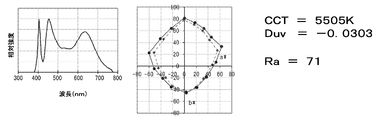
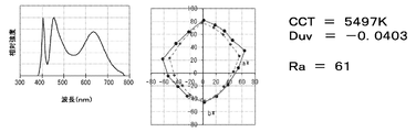
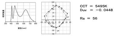
- the three types of spectral distributions (test light) shown in FIGS. 1, 2, and 3 include semiconductor light emitting elements having peak wavelengths of 425 to 475 nm, which are excited by green phosphors and red phosphors. This is an example in which the appearance of the color of the illuminated object is different in the same chromaticity (CCT is 5500 K, D uv is 0.0000), assuming a package LED as a light source.
- the green phosphor and red phosphor constituting the respective spectral distributions are assumed to be the same material, but the peak wavelength of the blue semiconductor light-emitting element is 459 nm in FIG. 1, 475 nm in FIG. In FIG. 3, it was 425 nm.
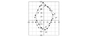
- the expected color appearance of the 15 color chart is shown in the CIELAB color space of FIGS. It becomes like.
- the points connected by dotted lines in the figure are cases where illumination with calculation reference light is assumed, and the solid lines are cases where illumination with respective test lights is assumed.
- the vertical direction on the paper is lightness, only the a * and b * axes are plotted here for convenience.
- Ra calculated from the spectral distribution shown in FIG. From the calculations assuming illumination with the reference light for calculation and the calculations assuming illumination with the test light in the figure, the appearance of the colors of the 15 color charts was expected to be close. Ra calculated from the spectral distribution was as high as 95. When it is assumed that the test light shown in FIG. 2 is illuminated, red and blue appear to be vivid, but purple and green are expected to be dull compared to the case where the test light is assumed to be illuminated. It was. Ra calculated from the spectral distribution was as low as 76. On the contrary, when it is assumed that the illumination is performed with the test light shown in FIG. 3, the purple and green appear to be vivid, but the red and blue are dull compared to the assumption that the illumination is performed with the calculation reference light. Was expected. Ra calculated from the spectral distribution was as low as 76. Thus, it can be understood that the appearance of the color can be changed at the same chromaticity point.
- the degree of freedom is low to change. Specifically, it was as follows.
- the present inventor mathematically compares the appearance of the color of the 15-color chart when different D uv values are given to a plurality of spectral distributions with a case where illumination with a calculation reference light is assumed. It was examined. In general, when D uv is positively biased, white appears to be greenish, when D uv is negative, white appears to be reddish, and when D uv is away from 0, the color appearance is unnatural as a whole. It is supposed to be visible. In particular, white coloring is believed to induce such perception.
- the present inventor has conducted the following studies in order to improve the controllability of the saturation.
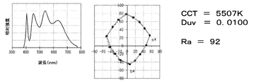
- the eight spectral distributions shown in FIGS. 4 to 11 include a blue semiconductor light emitting device having a peak wavelength of 459 nm, which is assumed to be a package LED using the green phosphor and the red phosphor as the excitation light source. This is a calculation result when D uv is changed from ⁇ 0.0500 to +0.0150 at (2700 K).
- the appearance of the colors of the 15 color charts expected when illumination with each spectral distribution (test light) is assumed and when illumination with calculation reference light for each test light is assumed is shown in FIG. It was as shown in CIELAB color space in FIG.
- the points connected by the dotted lines in the figure are the results of the reference light for calculation, and the solid lines are the results of the respective test lights.
- the vertical direction on the paper is lightness, only the a * and b * axes are plotted here for convenience.
- the test light in FIGS. 5 and 6 is an example in which D uv is shifted in the positive direction from +0.0100 to +0.0150.
- the appearance of the colors of the 15 kinds of color charts is excluding the blue-blue region when D uv is shifted in the positive direction. It was expected that almost all colors would appear dull.
- the saturation level decreased as D uv became positive. Ra calculated from the spectral distributions of FIGS. 5 and 6 was 94 and 89, respectively.
- the test light in FIGS. 7 to 11 is an example in which D uv is shifted in the negative direction from ⁇ 0.0100 to ⁇ 0.0500.
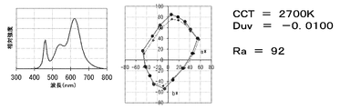
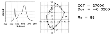
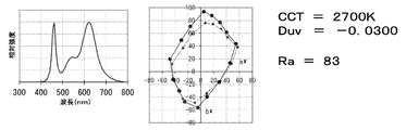
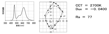
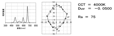
- FIG. 12 to FIG. 21 The 10 types of spectral distributions shown in FIG. 12 to FIG. 21 assume that the package LED containing four types of semiconductor light emitting elements is assumed and D uv is changed from ⁇ 0.0500 to +0.0400 in the same CCT (4000K). It is a result.
- the peak wavelengths of the four types of semiconductor light emitting devices were 459 nm, 528 nm, 591 nm, and 662 nm.
- Figure 10 shows the expected color appearance of the 15 color charts when assuming illumination with 10 types of test light and assuming illumination with reference light for calculation corresponding to each test light. 12 to CIELAB color space of FIG.
- the points connected by the dotted lines in the figure are the results of the calculation reference light
- the solid lines are the results of the respective test lights.
- the vertical direction on the paper is lightness, only the a * and b * axes are plotted here for convenience.
- the test light in FIGS. 13 to 16 is an example in which D uv is shifted in the positive direction from +0.0100 to +0.0400.
- the test light in FIGS. 17 to 21 is an example in which D uv is shifted in the negative direction from ⁇ 0.0100 to ⁇ 0.0500.
- the present invention gives various D uv values to the test light having different light-emitting elements (light-emitting materials) that form the spectrum
- the present inventors have developed the 15 most vivid colors on the outermost circumference of the modified Munsell color system. We examined mathematically what kind of color the votes would look like, comparing with the reference light for calculation.
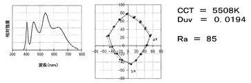
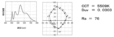
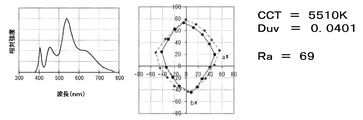
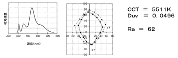
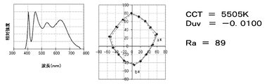
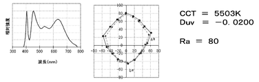
- the 11 types of spectral distributions shown in FIG. 22 to FIG. 32 are adjacent to each other, assuming a package LED in which a purple semiconductor light emitting element is inherently used as an excitation light source of a blue phosphor, a green phosphor, and a red phosphor.
- This is a calculation result when D uv is changed from ⁇ 0.0448 to +0.0496 in CCT (about 5500 K).
- the peak wavelength of the incorporated semiconductor light emitting device was 405 nm. Note that the result of FIG. 32 is a result realized without including a green phosphor so that D uv is extremely negative.
- FIG. The appearance of the color of the fifteen color charts predicted mathematically when assuming illumination with test light for each of the 11 types and assuming illumination with reference light for calculation with respect to the test light is shown in FIG. This is as shown in the CIELAB color space of FIG.
- the points connected by the dotted lines in the figure are the results of the reference light for calculation
- the solid lines are the results of the respective test lights.
- the vertical direction on the paper is lightness, only the a * and b * axes are plotted here for convenience.
- the test light in FIGS. 23 to 27 is an example in which D uv is shifted in the positive direction from +0.0100 to +0.0496.
- the test light in FIGS. 28 to 32 is an example in which D uv is shifted in the negative direction from ⁇ 0.0100 to ⁇ 0.0448.
- the hue angles of the 15 color charts are set to ⁇ nSSL (degrees) (where n is a natural number from 1 to 15), and the calculation reference light is selected according to the CCT of the test light.
- 5000K is the blackbody radiation light, in the above 5000K the CIE daylight
- the absolute value of the hue angle difference ⁇ h n (degree) (where n is a natural number from 1 to 15) of each of the 15 types of modified Munsell color charts when illuminated with the two lights is
- the following formula (1) which is an average value of the saturation difference of the 15 types of modified Munsell color charts, was also considered an important index.
- the index A cg is the difference between the color appearance due to the experimental reference light or the experimental pseudo reference light and the color appearance due to the test light, as a radiometric characteristic and a photometric characteristic of the spectral distribution or spectrum shape. I tried to describe it. As a result of various studies, the index A cg is defined as follows in the present invention.
- Spectral distributions of calculation reference light and test light that are color stimuli are ⁇ ref ( ⁇ ) and ⁇ SSL ( ⁇ ), respectively, and color matching functions are x ( ⁇ ), y ( ⁇ ), z ( ⁇ ), and for calculation
- ⁇ ref ( ⁇ ) and ⁇ SSL ( ⁇ ) color stimuli
- color matching functions are x ( ⁇ ), y ( ⁇ ), z ( ⁇ )
- tristimulus values corresponding to the reference light and the test light be (X ref , Y ref , Z ref ) and (X SSL , Y SSL , Z SSL ), respectively.
- k is a constant.
- Y ref k ⁇ ref ( ⁇ ) ⁇ y ( ⁇ ) d ⁇
- Y SSL k ⁇ SSL ( ⁇ ) ⁇ y ( ⁇ ) d ⁇
- S ref ( ⁇ ) ⁇ ref ( ⁇ ) / Y ref
- S SSL ( ⁇ ) ⁇ SSL ( ⁇ ) / Y SSL
- ⁇ S ( ⁇ ) S ref ( ⁇ ) ⁇ S SSL ( ⁇ ) It was.
- the index A cg is defined as follows.
- ⁇ 4 was defined separately in the following two cases.
- S SSL ( ⁇ ) the wavelength giving the longest wavelength maximum value within 380 nm to 780 nm is ⁇ R (nm), and the spectral intensity is S SSL ( ⁇ R ).
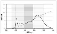
- the indicator A cg has a large visible range related to radiation that causes color stimulation, a short wavelength region (or a blue region including purple), an intermediate wavelength region (a green region including yellow), and a long wavelength region (a red region including orange). This is an index that determines whether or not there is unevenness in the spectrum at an appropriate position in the standardized test light spectral distribution compared to the mathematical standardized standard light spectral distribution. is there.
- the long wavelength integration range varies depending on the position of the longest wavelength maximum value.
- the selection of the reference light for calculation differs depending on the CCT of the test light. In the case of FIG.
- CIE daylight CIE daylight
- black body radiation light is selected as the reference light as indicated by the dotted line in the drawing.
- the shaded portion schematically shows the integration range of the short wavelength region, the intermediate wavelength region, and the long wavelength region.
- the first term of the index A cg (integral of ⁇ S ( ⁇ )) is a negative value when the spectral intensity of the normalized test light spectral distribution is stronger than the mathematical standardized reference light spectral distribution. It is easy to take.
- the second term of the index A cg (integral of ⁇ S ( ⁇ )) is negative. Easy to take value.
- the third term (integral of ⁇ S ( ⁇ )) of the index A cg has a negative value. It is an easy-to-take index.
- the calculation reference light is changed by the CCT of the test light. That is, as the reference light for calculation, black body radiation is used when the CCT of the test light is less than 5000K, and the defined CIE daylight (CIE daylight) is used when the CCT of the test light is 5000K or more. Used.
- CIE daylight CIE daylight
- ⁇ ref ( ⁇ ) uses the mathematically defined black body radiation or CIE daylight
- ⁇ SSL ( ⁇ ) is the function used in the simulation, Or the value actually measured by experiment was used.
- the radiation efficiency K (lm / W) of the distribution ⁇ SSL ( ⁇ ) is the efficiency that the spectral distribution has as its shape, and the efficiency related to all the material characteristics that constitute the light emitting device (for example, the internal quantum efficiency of the semiconductor light emitting element, When the light extraction efficiency, the internal quantum efficiency of the phosphor, the external quantum efficiency, the light transmission characteristics of the encapsulant, etc.) are 100%, the light source efficiency is ⁇ (lm / W).
- BAM or SBCA was used as the blue phosphor.
- BSS, ⁇ -SiAlON, or BSON was used as the green phosphor.
- YAG was used as the yellow phosphor.
- CASON or SCASN was used as the red phosphor.
- the usual method was used. Specifically, a semiconductor light emitting element (chip) was flip-chip mounted on a ceramic package in which a metal wiring capable of electrical conduction was contained. Next, the slurry which mixed the fluorescent substance and binder resin to be used was arrange
- LED bulbs After preparing package LEDs, they were used to make LED bulbs of MR16 Gu10, MR16 Gu5.3, and the like. This LED bulb incorporates a driving circuit, and is also equipped with a reflection mirror, a lens, etc., and finished in one kind of lighting fixture. Some commercially available LED bulbs were also prepared. In addition, an incandescent bulb containing a tungsten filament was also prepared as a reference light for experiments.
- LED bulbs were arranged to produce an illumination system for comparative visual experiments.
- One type of drive power line is dedicated to an incandescent lamp (experimental reference light) having a tungsten filament, and a variable transformer is arranged at the subsequent stage to increase the drive voltage from 110 V to 130 V with respect to an input voltage of 100 V.
- the CCT can be changed.
- the remaining two systems of the drive power line are for LED bulbs, one of which is for experimental pseudo reference light (LED light source), and the other one is for test light.
- test reference light or the experimental reference light
- test light were switched to allow the subject to evaluate the color appearance of many observation objects.
- the lighting system was installed in a dark room to eliminate disturbance.
- the illuminance at the position of the observation object was made approximately the same by changing the number of instruments of the experimental reference light (or experimental pseudo reference light) and test light mounted on the illumination system.
- the experiment was performed with the illuminance ranging from about 150 lx to about 5000 lx. Illustrated below are objects that are actually illuminated objects and observed objects.
- chromatic objects that cover all hues such as purple, blue-violet, blue, blue-green, green, yellow-green, yellow, yellow-red, red, and red-purple. Furthermore, achromatic objects such as white and black were also prepared. A lighting object having a color was prepared. Many kinds of still life, fresh flowers, food, clothing, printed matter, etc. were prepared. In the experiment, the subject's own skin was also observed. It should be noted that the color names partly added before the object names below are not strict color representations in the sense that they appear to be so under normal circumstances.
- the visual experiment was performed according to the following procedure. Prepared experimental reference light, experimental pseudo reference light, test light for each CCT measured at the position of the illumination object (according to the illumination method of the present invention), or prepared experimental reference light, experimental pseudo The light emitted in the main radiation direction of the reference light and the test light was measured, and classified into 6 experiments for each CCT (according to the light emitting device of the present invention). That is, it is as follows.
- the same object is illuminated by switching between experimental reference light (or experimental pseudo-reference light) and test light, and each light is natural and lively as seen outdoors.
- the subjects were asked to make a relative judgment as to whether high visibility and comfortable color appearance and object appearance could be realized. At that time, he asked why he was superior or inferior.
- the overall evaluation of the test light with respect to the reference light is centered on “0” indicating the same degree of appearance, the evaluation that the test light is slightly preferable is “1”, and the evaluation that the test light is preferable is “2”, the evaluation that the test light is more preferable is “3”, the evaluation that the test light is very preferable is “4”, and the evaluation that the test light is extremely preferable is “5”.
- the evaluation that test light is slightly unfavorable is “ ⁇ 1”
- the evaluation that test light is not preferable is “ ⁇ 2”
- the evaluation that test light is not preferable is “ ⁇ 3”
- the test light is very
- the evaluation that the test light is not preferable is “ ⁇ 4”
- the evaluation that the test light is not particularly preferable is “ ⁇ 5”.
- the fourth step in particular, in visual experiments, it was determined that the color appearance of the illumination object was better when illuminated with test light than when illuminated with experimental reference light or experimental reference light.
- test light The test light and comparative test light in the table may be collectively referred to as “test light”.
- Tables 4, 5, and 7 show that the D uv of the test light is the experimental reference light.
- the result on the positive side of the light (or the pseudo reference light for experiment) is included. From this, it can be seen that the more the test light D uv becomes positive, the more the subject is judged to be unfavorable regarding the color appearance of the illumination object and the appearance of the object. Specifically, it was as follows.
- the appearance of various illuminated chromatic colors becomes more unnatural as the D uv of the test light becomes more positive as compared to the case of illumination with the experimental reference light (or the experimental pseudo reference light).
- the subjects pointed out that the various color samples of the exterior wall materials that were illuminated were perceived very different from the color appearance seen outdoors, and that their skin color also looked unnatural and unhealthy.
- the D uv of the test light when the D uv of the test light is negative in the proper range and the various indicators in the table are in the proper range, it is compared with the case of illuminating with the experimental reference light (or the experimental reference light).
- the subject judged that the yellowishness (greenishness) was reduced, it looked slightly white, looked white, looked whiter, looked very white, and looked much whiter. He pointed out that the closer to the optimum range, the better the natural and better appearance. This was an unexpected result.
- the gray portion of the color checker is illuminated with experimental reference light (or experimental pseudo reference light) when the D uv of the test light is negative in the appropriate range and the various indicators in the table are in the appropriate range.
- each achromatic color chart also has an experimental reference light (or an experimental pseudo reference light) when the D uv of the test light is negative in the appropriate range and the various indicators in the table are in the appropriate range.
- the subject judged that it was slightly clearer, more clearly visible, more clearly visible, very clearly visible, and much more clearly visible than when illuminated in ().
- the subjects also noted that as they approached the optimal range, they became more natural and more visible. This was an unexpected result.
- the print characters in the negative in D uv is proper range of the test light, and, in the case various indices in the table is in the proper range, when illuminated by a laboratory reference light (or experimental pseudo reference light)
- the subjects judged that it was slightly easier to see, easier to see, easier to see, much easier to see, and much easier to see.
- the subjects also pointed out that as they approached the optimum range, the characters became more natural and more visible. This was an unexpected result.
- the color appearance of the various color samples of the outer wall material is such that when the D uv of the test light is negative within the proper range and the various indicators in the table are within the proper range, the experimental reference light (or the experimental pseudo reference) Compared to the case of illuminating with light), the memory when viewed outdoors was slightly close, close, close, very close, and much closer The subject judged that he was. The subjects also pointed out that as they approached the optimum range, they became more natural and looked like a favorable color closer to memory when viewed outdoors. This was an unexpected result.
- the appearance of the skin color of the subject himself is experimental reference light (or experiment) when the D uv of the test light is negative within the appropriate range and the various indicators in the table are within the appropriate range.
- the subject judged that it looked somewhat natural, looked natural, looked more natural, looked very natural, and looked much more natural than when illuminated with pseudo-standard light) .
- the subjects also pointed out that as they approached the optimal range, they became more natural and healthy in appearance. This was an unexpected result.
- the color difference of the same kind of similar color petals is the experimental reference light (or experimental pseudo reference light) when the D uv of the test light is negative within the appropriate range and the various indicators in the table are within the appropriate range.
- ) of the 15 color chart between the illumination by the test light and the illumination by the calculation reference light is relatively small, and the average saturation of the 15 color chart of the illumination by the test light However, it was higher in the appropriate range than that of the illumination with the reference light for calculation. Further, not only the average value but also the saturation degree ( ⁇ C n ) of the 15 color charts individually, each ⁇ C n of the 15 color charts of the illumination by the test light is different from those of the illumination by the reference light for calculation. In comparison, there is neither extremely decreased nor improved extremely, all are in the appropriate range, and as a result, the difference between the maximum and minimum saturation differences ( ⁇ C max ⁇ C min ) is in the appropriate range. It was narrow.
- the hue angle in all hues of the 15 color chart when the illumination with the test light is assumed as compared with the case where the illumination with the reference light is assumed for the 15 color chart, the hue angle in all hues of the 15 color chart. It can be inferred that the ideal is the case where the difference is small and the saturation of the 15 color chart is improved relatively evenly in an appropriate range.
- the solid line in FIG. 35 is the normalized test light spectral distribution of the test light 5 determined in Table 3 as “remarkably preferable” as a comprehensive judgment.
- the dotted line in the figure is the normalized spectral distribution of the reference light for calculation (black body radiation light) calculated from the CCT of the test light.
- FIG. 36 relates to the appearance of the color of the 15 color chart, assuming that the illumination is performed with the test light 5 (solid line) and the illumination with the reference light for calculation (light of black body radiation) (dotted line). CIELAB plot.
- the vertical direction on the paper is lightness, only the a * and b * axes are plotted here for convenience.
- FIGS. 37 and 38 summarize the results of the test light 15 determined as “remarkably preferable” as the overall determination in Table 5 in the same manner as described above.
- D uv in the illumination method according to the first embodiment of the present invention is ⁇ 0.0040 or less, slightly preferably ⁇ 0.0042 or less, preferably ⁇ 0.0070 or less, More preferably, it was ⁇ 0.0100 or less, very preferably ⁇ 0.0120 or less, and particularly preferably ⁇ 0.0160 or less.
- D uv in the illumination method according to the first embodiment of the present invention is ⁇ 0.0350 or more, slightly preferably ⁇ 0.0340 or more, and preferably ⁇ 0.0290 or more. More preferably, it is -0.0250 or more, very preferably -0.0230 or more, and particularly preferably -0.0200 or more.
- is 9.0 or less, very preferably 8.4 or less, and particularly preferably 7.3 or less. Further,
- the illumination method according to the first embodiment of the present invention Is 1.0 or more, slightly preferably 1.1 or more, preferably 1.9 or more, very preferably 2.3 or more, and particularly preferably 2. It was 6 or more. Moreover, it was 7.0 or less, Preferably it was 6.4 or less, Very preferably, it was 5.1 or less, Most preferably, it was 4.7 or less. In addition, the examination using the actual test light was made in the visual experiment, and the preferred range of the above index inside the preferred experimental result under the examination was 1.2 or more and 6.3 or less.
- ⁇ C n is ⁇ 3.8 or more, slightly preferably ⁇ 3.5 or more, and very preferably ⁇ 2.5 or more.
- the remarkably preferable value was ⁇ 0.7 or more.
- ⁇ C n in the lighting method according to the first embodiment of the present invention is 18.6 or less, very preferably 17.0 or less, and particularly preferably 15.0 or less.
- an examination using actual test light was performed in a visual experiment, and a preferable range of ⁇ C n inside a preferable experimental result under the examination was ⁇ 3.4 or more and 16.8 or less.
- ( ⁇ C max ⁇ C min ) is 19.6 or less, but is preferably 17.9 or less, and is preferably 15.2 or less. It was much better. In addition, it is considered more preferable that ( ⁇ C max ⁇ C min ) is small, and 14.0 or less is even more preferable, and 13.0 or less is considered to be very particularly preferable. In the illumination method according to the first embodiment of the present invention, ( ⁇ C max ⁇ C min ) was 2.8 or more, and the minimum value during the visual experiment was 3.16. Further, a study using a real test light was performed in a visual experiment, and a preferable range of ( ⁇ C max ⁇ C min ) inside a preferable experimental result under study was 3.2 or more and 17.8 or less. .
- the D uv value is as discussed above, and is ⁇ 0.0040 or less, slightly preferably ⁇ 0.0042 or less, and preferably ⁇ 0.0070 or less. More preferably, it was ⁇ 0.0100 or less, very preferably ⁇ 0.0120 or less, and much more preferably ⁇ 0.0160 or less. Further, D uv in the present invention is ⁇ 0.0350 or more, slightly preferably ⁇ 0.0340 or more, preferably ⁇ 0.0290 or more, more preferably ⁇ 0.0250 or more. Further, it was very preferably ⁇ 0.0230 or more, and particularly preferably ⁇ 0.0200 or more.
- the index A cg was as follows. From the results of Tables 2 to 7, the preferred spectral distribution of the illumination method according to the first embodiment of the present invention was A cg of ⁇ 10 or less and ⁇ 360 or more. The exact definition is as described above, but the approximate physical meaning and good interpretation are as follows.
- a cg takes a negative value in an appropriate range means that there is an appropriate unevenness in the standardized test light spectral distribution, and in the short wavelength region between 380 nm and 495 nm, the mathematical standardized reference light spectral distribution is Tends to have a higher radiant flux intensity of the normalized test light spectral distribution and / or in the intermediate wavelength region from 495 nm to 590 nm, the radiant flux of the normalized test light spectral distribution than the mathematical standardized reference light spectral distribution.
- a cg is the sum of the respective elements in the short wavelength region, the intermediate wavelength region, and the long wavelength region, each individual element may not necessarily have the above tendency.
- a cg is quantitatively ⁇ 10 or less and ⁇ 360 or more, good color appearance and good object appearance are obtained.
- a cg in the lighting method according to the first embodiment of the present invention is preferably ⁇ 10 or less, slightly preferably ⁇ 11 or less, more preferably ⁇ 28 or less, and very preferably.
- a cg is preferably ⁇ 360 or more, slightly preferably ⁇ 330 or more, and preferably ⁇ 260 or more. In particular, it was -181 or more, and particularly preferably -178 or more.
- the radiation efficiency of the spectral distribution by the illumination method according to the first embodiment of the present invention is preferably in the range of 180 (lm / W) to 320 (lm / W), and is a value of a normal incandescent bulb or the like. Was at least 20% higher than 150 (lm / W). This is considered to be because radiation from the semiconductor light emitting element and radiation from the phosphor are inherent, and there are appropriate irregularities at appropriate positions in the spectral distribution in relation to V ( ⁇ ). From the viewpoint of coexistence with color appearance, the radiation efficiency of the illumination method of the present invention is preferably in the following range.
- the radiation efficiency K by the illumination method according to the first embodiment of the present invention is preferably 180 (lm / W) or more, but is preferably 205 (lm / W) or more, preferably 208. (Lm / W) or more, and very preferably 215 (lm / W) or more.
- the radiation efficiency K is ideally high, but in the present invention, it is preferably 320 (lm / W) or less, and 282 (lm / W) or less from the balance with the color appearance. Is slightly preferred, preferably 232 (lm / W) or less, and particularly preferably 231 (lm / W) or less.
- the examination using the actual test light was made in the visual experiment, and the preferable range of K inside the preferable experiment result under the examination was 206 (lm / W) or more and 288 (lm / W) or less. .
- the CCT in the illumination method according to the first embodiment of the present invention is preferably slightly from 1800K to 15000K, preferably from 2000K to 10,000K, more preferably from 2300K to 7000K, and from 2600K to 6600K. It is very particularly preferred that it is 2900K to 5800K, most preferably 3400K to 5100K.
- the examination using the actual test light was made in the visual experiment, and the preferable range of CCT inside the preferable experimental result under the examination was 2550 (K) or more and 5650 (K) or less.
- the index A cg described in Tables 2 to 7 needs to be within an appropriate range in addition to D uv. It was. Further, various indexes, that is, radiation efficiency K (lm / W),
- D uv and index A cg were as follows from the result of the test light judged to be good in the visual experiment.
- the D uv value is ⁇ 0.0040 or less, slightly preferably ⁇ 0.0042 or less, preferably ⁇ 0.0070 or less, more preferably ⁇ 0.0100 or less. Therefore, it was very preferably ⁇ 0.0120 or less, and particularly preferably ⁇ 0.0160 or less. Further, D uv in the present invention is ⁇ 0.0350 or more, slightly preferably ⁇ 0.0340 or more, preferably ⁇ 0.0290 or more, more preferably ⁇ 0.0250 or more. Further, it was very preferably ⁇ 0.0230 or more, and particularly preferably ⁇ 0.0200 or more.
- the spectral distribution was A cg of ⁇ 10 or less and ⁇ 360 or more.
- the exact definition is as described above, but the approximate physical meaning and good interpretation are as follows.
- a cg takes a negative value in an appropriate range means that there is an appropriate unevenness in the standardized test light spectral distribution, and in the short wavelength region between 380 nm and 495 nm, the mathematical standardized reference light spectral distribution is Tends to have a higher radiant flux intensity of the normalized test light spectral distribution and / or in the intermediate wavelength region from 495 nm to 590 nm, the radiant flux of the normalized test light spectral distribution than the mathematical standardized reference light spectral distribution.
- the intensity tends to be weak and / or, in the long wavelength region from 590 nm to ⁇ 4, the radiant flux intensity of the normalized test light spectral distribution tends to be stronger than the mathematical standardized reference light spectral distribution. is doing.
- a cg is quantitatively ⁇ 10 or less and ⁇ 360 or more, good color appearance and good object appearance are obtained.
- a cg derived from the spectral distribution of light emitted in the main radiation direction from the light emitting device according to the second embodiment of the present invention is ⁇ 10 or less, preferably slightly ⁇ 11 or less, and more It was preferably -28 or less, very preferably -41 or less, and particularly preferably -114 or less. Further, A cg derived from the spectral distribution of the light emitted in the main radiation direction from the light emitting device according to the second embodiment of the present invention is ⁇ 360 or more, and is preferably ⁇ 330 or more, It was preferably -260 or more, very preferably -181 or more, and particularly preferably -178 or more. Incidentally, consider using real test light in the visual experiments have been made, the preferable range of A cg inside the preferred experimental results in the study, -322 or higher, was -12.
- the radiation efficiency of the spectral distribution by the light emitting device according to the second embodiment of the present invention is preferably in the range of 180 (lm / W) to 320 (lm / W), and is a value of a normal incandescent bulb or the like. Was at least 20% higher than 150 (lm / W). This is considered to be because radiation from the semiconductor light emitting element and radiation from the phosphor are inherent, and there are appropriate irregularities at appropriate positions in the spectral distribution in relation to V ( ⁇ ). From the standpoint of compatibility with color appearance, the following range is preferable for the radiation efficiency obtained from the spectral distribution of the light emitted in the main radiation direction from the light emitting device according to the second embodiment of the present invention. It was.
- the radiation efficiency K of the light emitting device according to the second embodiment of the present invention is preferably 180 (lm / W) or more, but is preferably 205 (lm / W) or more, preferably 208. (Lm / W) or more, and very preferably 215 (lm / W) or more.
- the radiation efficiency K is ideally high, but in the present invention, it is preferably 320 (lm / W) or less, and 282 (lm / W) or less from the balance with the color appearance. Is slightly preferred, preferably 232 (lm / W) or less, and particularly preferably 231 (lm / W) or less.
- the examination using the actual test light was made in the visual experiment, and the preferable range of K inside the preferable experiment result under the examination was 206 (lm / W) or more and 288 (lm / W) or less. .
- ) of the 15 color chart between the illumination by the test light and the illumination by the calculation reference light is relatively small, and the average saturation of the 15 color chart of the illumination by the test light However, it was higher in the appropriate range than that of the illumination with the reference light for calculation. Further, not only the average value but also the saturation degree ( ⁇ C n ) of the 15 color charts individually, each ⁇ C n of the 15 color charts of the illumination by the test light is different from those of the illumination by the reference light for calculation. In comparison, there is neither extremely decreased nor improved extremely, all are in the appropriate range, and as a result, the difference between the maximum and minimum saturation differences ( ⁇ C max ⁇ C min ) is in the appropriate range. It was narrow.
- the hue angle in all hues of the 15 color chart when the illumination with the test light is assumed as compared with the case where the illumination with the reference light is assumed for the 15 color chart, the hue angle in all hues of the 15 color chart. It can be inferred that the ideal is the case where the difference is small and the saturation of the 15 color chart is improved relatively evenly in an appropriate range.
- the solid line in FIG. 35 is the normalized test light spectral distribution of the test light 5 determined in Table 3 as “remarkably preferable” as a comprehensive judgment.
- the dotted line in the figure is the normalized spectral distribution of the reference light for calculation (black body radiation light) calculated from the CCT of the test light.
- FIG. 36 relates to the appearance of the color of the 15 color chart, assuming that the illumination is performed with the test light 5 (solid line) and the illumination with the reference light for calculation (light of black body radiation) (dotted line). CIELAB plot.
- the vertical direction on the paper is lightness, only the a * and b * axes are plotted here for convenience.
- FIGS. 37 and 38 summarize the results of the test light 15 determined as “remarkably preferable” as the overall determination in Table 5 in the same manner as described above.
- D uv in the light emitting device according to the second embodiment of the present invention is ⁇ 0.0040 or less, slightly preferably ⁇ 0.0042 or less, and preferably ⁇ 0.0070 or less. More preferably, it was ⁇ 0.0100 or less, very preferably ⁇ 0.0120 or less, and particularly preferably ⁇ 0.0160 or less.
- D uv in the light emitting device according to the second embodiment of the present invention is ⁇ 0.0350 or more, slightly preferably ⁇ 0.0340 or more, and preferably ⁇ 0.0290 or more. More preferably, it was -0.0250 or more, very preferably -0.0230 or more, and much more preferably -0.0200 or more.
- is preferably 9.0 or less, very preferably 8.4 or less, and particularly preferably 7.3 or less. . Further,
- is preferably 0 or more, and the minimum value during a visual experiment is 0.0029. Furthermore, examination using actual test light was performed in a visual experiment, and a preferable range of
- the light emitting device Is preferably 1.0 or more, slightly preferably 1.1 or more, preferably 1.9 or more, very preferably 2.3 or more, and particularly preferably 2 .6 or more. Also, it is preferably 7.0 or less, preferably 6.4 or less, very preferably 5.1 or less, and particularly preferably 4.7 or less.
- the examination using the actual test light was made in the visual experiment, and the preferred range of the above index inside the preferred experimental result under the examination was 1.2 or more and 6.3 or less.
- ⁇ C n in the light emitting device according to the second embodiment of the present invention is preferably ⁇ 3.8 or more, more preferably ⁇ 3.5 or more, and most preferably ⁇ 2. It was 5 or more, and particularly preferably ⁇ 0.7 or more.
- ⁇ C n in the light emitting device according to the second embodiment of the present invention is preferably 18.6 or less, very preferably 17.0 or less, and particularly preferably 15. 0 or less.
- a visual test was performed using actual test light, and a preferable range of ⁇ C n inside the preferable experimental result under consideration was ⁇ 3.4 or more and 16.8 or less.
- ( ⁇ C max ⁇ C min ) is preferably 19.6 or less, very preferably 17.9 or less, and 15.2 or less. It was much better to be. In addition, it is considered more preferable that ( ⁇ C max ⁇ C min ) is small, and 14.0 or less is even more preferable, and 13.0 or less is considered to be very particularly preferable. In the light emitting device according to the second embodiment of the present invention, ( ⁇ C max ⁇ C min ) is preferably 2.8 or more, and the minimum value during the visual experiment is 3.16. Further, a study using a real test light was performed in a visual experiment, and a preferable range of ( ⁇ C max ⁇ C min ) inside a preferable experimental result under study was 3.2 or more and 17.8 or less. .
- CCT in the light emitting device according to the second embodiment of the present invention.
- Various indexes determined to be preferable by comparative visual experiments, that is,
- ⁇ C n and ( ⁇ C max ⁇ C min ) it is preferable that the CCT take a value close to 4000 K in the light emitting device according to the second embodiment of the present invention. This is because the spectral distribution of light near 4000K is isoenergetic without much dependence on wavelength even when the reference light is viewed, and a test light spectral distribution in which irregularities are easily formed with respect to the reference light is realized. This is thought to be possible. In other words,
- the CCT in the light emitting device is slightly preferably from 1800K to 15000K, more preferably from 2000K to 10,000K, more preferably from 2300K to 7000K, and from 2600K to 6600K. It is very particularly preferred that it is 2900K to 5800K, most preferably 3400K to 5100K.
- the examination using the actual test light was made in the visual experiment, and the preferable range of CCT inside the preferable experimental result under the examination was 2550 (K) or more and 5650 (K) or less.
- the fifteen colors are assumed assuming that the photometric characteristics of the test light that is emitted to the object to be illuminated and is a color stimulus are in an appropriate range and are illuminated with the reference light for calculation. If the difference between the color appearance of the vote and the color appearance of the 15-color chart assuming the illumination with the measured test light spectral distribution is within an appropriate range, there are no restrictions on the configuration, material, and the like of the light emitting device.
- the light-emitting device of the present invention emits light from the light-emitting device in the main radiation direction, and the light-measuring device is suitable if the radiometric characteristics and the photometric characteristics of the test light that is a color stimulus for the illumination object are within an appropriate range. There are no restrictions on the configuration, materials, etc.
- a light emitting device for implementing the illumination method or the light emitting device of the present invention a lighting device including the lighting light source, a light emitting device such as a lighting system including the lighting light source or the lighting device, and a semiconductor light emitting element that is at least one light emitting element Is included.
- the illumination light source including the semiconductor light emitting element may include, for example, a plurality of semiconductor light emitting elements of different types of blue, green, and red in one illumination light source.
- the light emitted as the lighting system may satisfy the desired characteristics at the position of the lighting object by additive color mixing with light from different lighting fixtures existing in the lighting system.
- the light in the main radiation direction among the light emitted as the illumination system may satisfy the desired characteristics.
- the light as the color stimulus that is finally irradiated to the illumination object or the light in the main radiation direction among the light emitted from the light emitting device is suitable for the present invention. It only has to satisfy the conditions.
- the light-emitting device for carrying out the illumination method according to the first embodiment of the present invention and the light-emitting device according to the second embodiment of the present invention are preferably satisfied after satisfying the appropriate conditions. Describe the properties that should be present.
- the light-emitting device for performing the illumination method according to the first embodiment of the present invention or the light-emitting device according to the second embodiment of the present invention is within a short wavelength region of ⁇ 1 (380 nm) to ⁇ 2 (495 nm). And another light emitting element (luminescent material) having a peak in the intermediate wavelength region of ⁇ 2 (495 nm) to ⁇ 3 (590 nm), and ⁇ 3 ( It is preferable to have another light emitting element (light emitting material) having a peak in a long wavelength region from 590 nm to 780 nm. This is because it is possible to easily realize a preferable color appearance by independently setting or controlling the intensity of each light emitting element.
- the light-emitting device for implementing the illumination method according to the first embodiment of the present invention or the light-emitting device according to the second embodiment of the present invention has a light emission peak in each of the above three wavelength regions. It is preferable to have at least one type of light-emitting element (light-emitting material), one type in two of the three wavelength regions, and the other one region to have a plurality of light-emitting elements (light-emitting materials). More preferably, it is very preferable that one of the three wavelength regions has one kind and the other two regions have a plurality of light emitting elements (light emitting materials). It is particularly preferred to have a light emitting element. This is because the control of the spectral distribution is remarkably improved by incorporating the light-emitting elements so as to have two or more peak wavelengths in one region, and mathematically, the color appearance of the illuminated object is desired. This is because it becomes easier to control.
- an actual light-emitting device using a semiconductor light-emitting element as an excitation light source for a phosphor there are two types of phosphors in one light-emitting device, and the peak wavelength is set in each of the three wavelength regions together with the wavelength of the semiconductor light-emitting element. It is preferable to have. Furthermore, it is more preferable that there are three types of phosphors, and two types of light emitting elements are present in at least one of the three wavelength regions together with the wavelength of the semiconductor light emitting element. From such an idea, 4 or more types of phosphors are very preferable, and 5 types are extremely preferable.
- the controllability of the spectrum is adversely reduced due to mutual absorption between the phosphors.
- the phosphor type may be one, and the light-emitting device may be configured with two types of light-emitting elements together with the light emission peak of the semiconductor light-emitting element. I do not care.
- the blue light emitting element and two kinds of phosphors may be mounted in one light source.
- the element and three types of phosphors may be mounted in one light source.
- a single light source is equipped with a blue light emitting element and two types of phosphors (green and red), and a purple light emitting element and three types of phosphors (blue, green and red). The portion that is present may be included.
- At least one of the light emitting elements (light emitting materials) in each of the three wavelength regions is relatively It preferably includes a narrow band light emitting element.
- the light emitting element having a relatively narrow band may be a light emitting element in a wavelength region where only the light emitting element is present, but there are a plurality of types of light emitting elements having a relatively narrow band in the wavelength region. It is more preferable that the light emitting element having a relatively narrow band and the light emitting element having a relatively wide band are both present in the wavelength region.
- the comparatively narrow band here means that the full width at half maximum of the light emitting element (light emitting material) is a short wavelength region (380 nm to 495 nm), an intermediate wavelength region (495 nm to 590 nm), and a long wavelength region (590 nm to 780 nm). That is, 2/3 or less with respect to the respective region widths of 115 nm, 95 nm, and 190 nm.
- the full width at half maximum is preferably 1/2 or less, more preferably 1/3 or less, and 1/4 or less with respect to the width of each region. It is very preferable that it is 1/5 or less.
- the full width at half maximum is preferably 2 nm or more, and 4 nm or more. More preferably, 6 nm or more is very preferable, and 8 nm or more is particularly preferable.
- the index A cg , the radiation efficiency K (lm / W), and the like are preferable because they are easily set to desired values.
- the difference between the color appearance of the 15 color chart when the light is regarded as a color stimulus and the illumination with the light emitting device is assumed and the color appearance when the illumination with the calculation reference light is assumed.
- a relatively narrow band in the light emitting element a suitable range has been revealed by saturation control, particularly visual experiments
- the following light-emitting material, phosphor material, and semiconductor light-emitting element are inherent in the light-emitting device as light-emitting elements.
- heat radiation from a hot filament discharge radiation from a fluorescent tube, high pressure sodium lamp, etc., laser, etc.
- any light source such as spontaneous emission light, spontaneous emission light from a semiconductor light emitting element, spontaneous emission light from a phosphor, and the like.
- light emission from a photoexcited phosphor, light emission from a semiconductor light emitting element, and light emission from a semiconductor laser are preferable because they are small in size, high in energy efficiency, and capable of relatively narrow band light emission.
- a purple light emitting element peak wavelength is about 395 nm to about 420 nm
- a blue purple light emitting element peak A blue light emitting element (having a peak wavelength of about 455 nm to 485 nm) is preferable.
- a blue light emitting element peak wavelength is about 455 nm to 485 nm
- Zn (Cd) (S) Se-based material formed on a GaAs substrate in the active layer structure is also preferable.
- the spectral distribution of the radiant flux exhibited by light emitting elements (light emitting materials) such as semiconductor light emitting elements and phosphors, and the peak wavelength thereof are the ambient temperature, the heat radiation environment of light emitting devices such as packages and lamps, injection current, circuit configuration, Or, in some cases, it is usually slightly changed due to deterioration or the like. Therefore, a semiconductor light emitting device having a peak wavelength of 418 nm under a certain driving condition may exhibit a peak wavelength of 421 nm, for example, when the temperature of the surrounding environment increases.
- the spectral distribution of the radiant flux and the peak wavelength exhibited by light emitting elements (light emitting materials) such as semiconductor light emitting elements and phosphors described below.
- the active layer structure may be a multiple quantum well structure in which a quantum well layer and a barrier layer are stacked, or a single or double hetero structure including a relatively thick active layer and a barrier layer (or a clad layer), which consists of a single pn junction. It may be homozygous.
- the blue-violet light-emitting element and the violet light-emitting element whose In concentration is lower in the active layer structure than the blue light-emitting element are emitted by the segregation of In. This is preferable because fluctuation is reduced and the full width at half maximum of the emission spectrum is reduced. Further, the blue-violet light-emitting element and the violet light-emitting element are preferable because they are positioned relatively on the outer side (short wavelength side) of wavelengths from 380 nm to 495 nm, which is the wavelength region, and D uv can be easily controlled.
- the semiconductor light emitting device having a light emission peak in the short wavelength region of ⁇ 1 (380 nm) to ⁇ 2 (495 nm) is preferably a blue light emitting device (peak wavelength is about 455 nm to 485 nm), and a blue-violet color having a shorter wavelength than this.
- a light emitting element peak wavelength is about 420 nm to about 455 nm
- a purple light emitting element peak wavelength is about 395 nm to about 420 nm
- a semiconductor laser As the light emitting element.
- a blue semiconductor laser (oscillation wavelength is about 455 nm to 485 nm) is preferable, and a blue-violet semiconductor laser having a longer wavelength (oscillation wavelength from 420 nm) is preferable.
- About 455 nm) is more preferable, and a violet semiconductor laser (with an oscillation wavelength of about 395 nm to 420 nm) is very preferable.
- the semiconductor light emitting element in the short wavelength region used in the illumination method or the light emitting device of the present invention preferably has a narrow full width at half maximum of its emission spectrum.
- the full width at half maximum of the semiconductor light emitting element used in the short wavelength region is preferably 45 nm or less, more preferably 40 nm or less, very preferably 35 nm or less, and particularly preferably 30 nm or less.
- the full width at half maximum of the semiconductor light emitting element used in the short wavelength region is 2 nm or more. Is preferable, 4 nm or more is more preferable, 6 nm or more is very preferable, and 8 nm or more is particularly preferable.
- the semiconductor light emitting element in the short wavelength region used in the illumination method or the light emitting device of the present invention preferably includes an In (Al) GaN-based material in the active layer structure, it is formed on a sapphire substrate or a GaN substrate.
- a light emitting element is preferable.
- the degree of In segregation in the active layer of the light emitting device formed on the GaN substrate is better than that formed on the sapphire substrate. This depends on the lattice matching between the substrate and the active layer structure material. For this reason, since the full width at half maximum of the In (Al) GaN emission spectrum on the GaN substrate can be made narrower, a remarkable synergistic effect with the present invention can be expected, which is very preferable.
- the element formed especially on the semipolar surface and the nonpolar surface is preferable. This reduces the piezoelectric polarization effect with respect to the crystal growth direction, which increases the spatial overlap of the spatial electron and hole wave functions in the quantum well layer, which in principle improves luminous efficiency and narrows the spectrum. This is because bandwidth can be realized. Therefore, it is very preferable to use a semiconductor light emitting element on a semipolar or nonpolar GaN substrate because a remarkable synergistic effect with the present invention can be expected.
- the substrate is either thick or completely peeled from the semiconductor light emitting device.
- the substrate is preferably thick, preferably 100 ⁇ m or more, more preferably 200 ⁇ m or more, so as to facilitate light extraction from the side wall of the GaN substrate. 400 ⁇ m or more is very preferable, and 600 ⁇ m or more is particularly preferable.
- the thickness of the substrate is preferably 2 mm or less, more preferably 1.8 mm or less, very preferably 1.6 mm or less, and particularly preferably 1.4 mm or less from the viewpoint of device preparation.
- the substrate is preferably peeled off by a method such as laser lift-off.
- a method such as laser lift-off.
- the stress applied to the quantum well layer that promotes the broadband due to the extreme lattice mismatch with the substrate is reduced, and as a result, the spectrum of the light emitting element can be narrowed. Therefore, a light-emitting element from which a sapphire substrate or the like is peeled off can be expected to have a remarkable synergistic effect with the present invention, which is very preferable.
- the full width at half maximum is preferably narrow.
- the full width at half maximum of the emission spectrum of the phosphor material used in the short wavelength region when excited at room temperature is preferably 90 nm or less, more preferably 80 nm or less, very preferably 70 nm or less, and particularly 60 nm or less. Is preferable.
- the full width at half maximum of the phosphor material used in the short wavelength region is 2 nm or more. Is preferable, 4 nm or more is more preferable, 6 nm or more is very preferable, and 8 nm or more is particularly preferable.
- the phosphor material in the short wavelength region preferably has a peak wavelength in the following range in consideration of the convenience of exciting the phosphor material and the controllability of D uv .
- the peak wavelength is preferably 455 nm to 485 nm, and more preferably 420 nm to 455 nm, which is shorter than this.
- the peak wavelength is preferably from 455 nm to 485 nm, more preferably from 420 nm to 455 nm, which is shorter than this, and the peak wavelength is very preferably from 395 nm to 420 nm. .
- Eu2 + is an activator and alkaline earth aluminin.
- thermal radiation from a hot filament, discharge radiation from a fluorescent tube, high-pressure sodium lamp, etc. nonlinear optical effect
- any light source such as stimulated emission light from a laser including second harmonic generation (SHG) using SEM, spontaneous emission light from a semiconductor light emitting device, spontaneous emission light from a phosphor, etc.
- SHG second harmonic generation
- spontaneous emission light from a semiconductor light emitting device spontaneous emission light from a phosphor, etc.
- light emission from a photoexcited phosphor, light emission from a semiconductor light emitting element, light emission from a semiconductor laser, and an SHG laser are preferable because they are small in size, high in energy efficiency, and capable of relatively narrow band light emission. .
- a blue-green light emitting device peak wavelength is about 495 nm to about 500 nm
- a green light emitting device peak wavelength is 500 nm
- an In (Al) GaN-based material on a sapphire substrate or a GaN substrate in an active layer structure.
- a yellow-green light emitting element peak wavelength is about 530 nm to 570 nm
- a yellow light emitting element peak wavelength is about 570 nm to 580 nm).
- a yellow-green light emitting element by GaP on the GaP substrate peak wavelength is about 530 nm to 570 nm
- a yellow light emitting element by GaAsP on the GaP substrate peak wavelength is about 570 nm to 580 nm
- a yellow light emitting element (peak wavelength is about 570 nm to about 580 nm) by AlInGaP on a GaAs substrate is also preferable.
- the active layer structure may be a multiple quantum well structure in which a quantum well layer and a barrier layer are stacked, or a single or double hetero structure including a relatively thick active layer and a barrier layer (or a clad layer), which consists of a single pn junction. It may be homozygous.
- the yellow-green light-emitting element, the green light-emitting element, and the blue-green light-emitting element whose In concentration is lower in the active layer structure than the yellow light-emitting element are segregated in In. Is preferable because the fluctuation of the emission wavelength due to is reduced and the full width at half maximum of the emission spectrum is reduced.
- the semiconductor light emitting device having a light emission peak in the intermediate wavelength region of ⁇ 2 (495 nm) to ⁇ 3 (590 nm) is preferably a yellow light emitting device (peak wavelength is about 570 nm to 580 nm), and a yellowish green having a shorter wavelength than this.
- a light emitting element peak wavelength is about 530 nm to 570 nm
- a green light emitting element having a shorter wavelength peak wavelength is about 500 nm to about 530 nm
- a blue-green light emitting element peak wavelength is about 495 nm to about 500 nm). It is particularly preferable.
- the oscillation wavelength is preferably in the yellow (peak wavelength is about 570 nm to 580 nm) region for the same reason as described above, and in the yellow-green region (the peak wavelength is about 530 nm to 570 nm) shorter than this. More preferably, it is very preferable to be in the green region (peak wavelength is about 500 nm to 530 nm) with a shorter wavelength than this, and it is particularly preferable to be in the blue green region (peak wavelength is about 495 nm to 500 nm). Is preferred.
- the semiconductor light emitting element in the intermediate wavelength region used in the illumination method or the light emitting device of the present invention preferably has a narrow full width at half maximum of its emission spectrum.
- the full width at half maximum of the semiconductor light emitting element used in the intermediate wavelength region is preferably 75 nm or less, more preferably 60 nm or less, very preferably 50 nm or less, and particularly preferably 40 nm or less.
- the full width at half maximum of the semiconductor light emitting element used in the intermediate wavelength region is 2 nm or more. Is preferable, 4 nm or more is more preferable, 6 nm or more is very preferable, and 8 nm or more is particularly preferable.
- the semiconductor light emitting device in the intermediate wavelength region used in the present invention is preferably a light emitting device formed on a sapphire substrate or a GaN substrate when an In (Al) GaN-based material is included in the active layer structure.
- a light emitting element formed on a GaN substrate is more preferable.
- a light emitting element in the intermediate wavelength region on the GaN substrate is preferable because a remarkable synergistic effect is expected. Furthermore, even if it is a light emitting element on a GaN substrate, the element formed especially on the semipolar surface and the nonpolar surface is preferable.
- the thickness of the substrate is either thick or completely removed.
- the substrate is preferably thick, preferably 100 ⁇ m or more, more preferably 200 ⁇ m or more, so as to facilitate light extraction from the side wall of the GaN substrate. 400 ⁇ m or more is very preferable, and 600 ⁇ m or more is particularly preferable.
- the thickness of the substrate is preferably 2 mm or less, more preferably 1.8 mm or less, very preferably 1.6 mm or less, and particularly preferably 1.4 mm or less from the viewpoint of device preparation.
- the substrate is preferably thick, preferably 100 ⁇ m or more, and 200 ⁇ m or more so as to promote light extraction from the GaP substrate side wall. More preferably, 400 ⁇ m or more is very preferable, and 600 ⁇ m or more is particularly preferable.
- the thickness of the substrate is preferably 2 mm or less, more preferably 1.8 mm or less, very preferably 1.6 mm or less, and particularly preferably 1.4 mm or less from the viewpoint of device preparation.
- the band gap of the substrate is smaller than the band gap of the material forming the active layer structure, so that light in the emission wavelength region is absorbed.
- substrate is thin is preferable, and the case where it peeled completely from the semiconductor light-emitting device is preferable.
- a semiconductor light emitting element is formed on a sapphire substrate or the like, it is preferable to peel off the substrate by a method such as laser lift-off.
- a method such as laser lift-off.
- the stress applied to the quantum well layer which is broadened due to an extreme lattice mismatch with the substrate, is reduced, and as a result, the spectrum of the light emitting element can be narrowed. Therefore, a semiconductor light emitting device from which a sapphire substrate or the like is peeled off can be expected to have a significant synergistic effect with the present invention, and is very preferable.
- the full width at half maximum of the phosphor material in the intermediate wavelength region used in the illumination method or the light emitting device of the present invention is narrow.
- the full width at half maximum of the emission spectrum of the phosphor material used in the intermediate wavelength region when excited at room temperature is preferably 130 nm or less, more preferably 110 nm or less, very preferably 90 nm or less, and particularly 70 nm or less. Is preferred.
- the full width at half maximum of the phosphor material used in the intermediate wavelength region is 2 nm or more.
- the peak wavelength is preferably from 495 nm to 500 nm, the peak wavelength is from 500 nm to 530 nm, and the peak wavelength is from 570 nm to 580 nm. The case is more preferred to the same extent, and the peak wavelength is very preferably from 530 nm to 570 nm.
- any phosphor material satisfying the full width at half maximum can be preferably used.
- Specific examples thereof include green phosphors containing Eu 2+ , Ce 3+, etc. as activators.
- a preferred green phosphor using Eu 2+ as an activator is a green phosphor based on a crystal composed of alkaline earth silicate, alkaline earth silicate nitride or sialon. This type of green phosphor can usually be excited using ultraviolet to blue semiconductor light emitting devices.
- an alkaline earth silicate crystal as a base examples include a phosphor represented by the following general formula (6) and a phosphor represented by the following general formula (6) ′.
- the alkaline earth silicate represented by the general formula (6) is referred to as a BSS phosphor.
- Ba 1-xy Sr x Eu y Mg 1-z Mn z Al 10 O 17 (6) ′ (In the general formula (6) ′, x, y, and z satisfy 0.1 ⁇ x ⁇ 0.4, 0.25 ⁇ y ⁇ 0.6, and 0.05 ⁇ z ⁇ 0.5, respectively.)
- the alkaline earth aluminate phosphor represented by the formula (6) ′ is referred to as a G-BAM phosphor.
- a specific example of a material having a sialon crystal as a base includes a phosphor represented by Si 6-z Al z O z N 8-z : Eu (where 0 ⁇ z ⁇ 4.2) (this is expressed as ⁇ - Called SiAlON phosphor).
- Suitable green phosphors using Ce 3+ as an activator include green phosphors based on garnet-type oxide crystals, such as Ca 3 (Sc, Mg) 2 Si 3 O 12 : Ce and alkaline earths There are green phosphors based on metal scandate crystals, such as CaSc 2 O 4 : Ce.
- Other examples include SrGaS 4 : Eu 2+ .
- Still another example is an oxynitride phosphor represented by (Ba, Ca, Sr, Mg, Zn, Eu) 3 Si 6 O 12 N 2 (this is referred to as a BSON phosphor).
- YAG phosphor Yttrium / aluminum / garnet-based phosphor
- Ca 1.5x La 3-X Si 6 N 11 Ce (where x is 0 ⁇ x ⁇ 1), and a lanthanum silicon nitride phosphor (referred to as an LSN phosphor).
- BSS phosphors BSS phosphors, ⁇ -SiAlON phosphors, BSON phosphors, G-BAM phosphors, YAG phosphors, SrGaS 4 : Eu 2+ phosphors and the like can be preferably exemplified.
- Light emitted from any light source such as light, spontaneous emission from a semiconductor light emitting device, spontaneous emission from a phosphor, and the like can be included.
- light emission from a photoexcited phosphor, light emission from a semiconductor light emitting element, and light emission from a semiconductor laser are preferable because they are small in size, high in energy efficiency, and capable of relatively narrow band light emission.
- the semiconductor light emitting element an AlGaAs material formed on a GaAs substrate, an orange light emitting element including an (Al) InGaP material formed on a GaAs substrate in an active layer structure (peak wavelength is about 590 nm to about 600 nm), Red light emitting elements (600 nm to 780 nm) are preferred.
- a red light emitting element (600 nm to 780 nm) including a GaAsP-based material formed on a GaP substrate in the active layer structure is preferable.
- the active layer structure may be a multiple quantum well structure in which a quantum well layer and a barrier layer are stacked, or a single or double hetero structure including a relatively thick active layer and a barrier layer (or a clad layer), which consists of a single pn junction. It may be homozygous.
- the peak wavelength is preferably close to 630 nm in consideration of both D uv controllability and radiation efficiency.
- the red light emitting element is more preferable than the orange light emitting element. That is, in the present invention, the semiconductor light emitting device having an emission peak in the long wavelength region from ⁇ 3 (590 nm) to 780 nm is preferably an orange light emitting device (peak wavelength is about 590 nm to 600 nm), and a red light emitting device (peak wavelength is 600 nm to 780 nm).
- a red light emitting element having a peak wavelength close to about 630 nm is very preferable.
- a red light emitting device having a peak wavelength of 615 nm to 645 nm is very preferable.
- the oscillation wavelength preferably has an oscillation wavelength in an orange (peak wavelength is about 590 to 600 nm) region, and has an oscillation wavelength in a red (peak wavelength about 600 to 780 nm) region. More preferably, the oscillation wavelength is very preferably in the red region close to about 630 nm. In particular, a red semiconductor laser having an oscillation wavelength of 615 nm to 645 nm is very preferable.
- the long wavelength full width at half maximum of the semiconductor light emitting element in the long wavelength region used in the illumination method or the light emitting device of the present invention is preferably narrow.
- the full width at half maximum of the semiconductor light emitting element used in the long wavelength region is preferably 30 nm or less, more preferably 25 nm or less, very preferably 20 nm or less, and particularly preferably 15 nm or less.
- the full width at half maximum of the semiconductor light emitting element used in the long wavelength region is 2 nm or more. Is preferable, 4 nm or more is more preferable, 6 nm or more is very preferable, and 8 nm or more is particularly preferable.
- the band gap of the GaAs substrate is smaller than the band gap of the material forming the active layer structure, light in the emission wavelength region is absorbed. For this reason, it is preferable that the thickness of the substrate is thin, and it is preferable that the substrate is completely removed.
- the full width at half maximum of the phosphor material in the long wavelength region used in the illumination method or the light emitting device of the present invention is narrow.
- the full width at half maximum of the emission spectrum of the phosphor material used in the long wavelength region when excited at room temperature is preferably 130 nm or less, more preferably 110 nm or less, very preferably 90 nm or less, and particularly 70 nm or less. Is preferred.
- the full width at half maximum of the phosphor material used in the long wavelength region is 2 nm or more.
- the peak wavelength may be close to 630 nm when a light emitting device is manufactured as a unit with other materials in consideration of both D uv controllability and radiation efficiency.
- a phosphor material having an emission peak in a long wavelength region from ⁇ 3 (590 nm) to 780 nm preferably has a peak between 590 nm and 600 nm, and has a peak at about 600 nm to 780 nm. It is more preferable that the peak wavelength is close to 630 nm.
- a phosphor material having a peak wavelength of 620 nm to 655 nm is very preferable.
- any phosphor material satisfying the full width at half maximum can be preferably used.
- Specific examples thereof include phosphors having Eu 2+ as an activator and based on a crystal made of alkaline earth silicon nitride, ⁇ sialon or alkaline earth silicate. This type of red phosphor can usually be excited using ultraviolet to blue semiconductor light emitting devices.
- Specific examples of an alkaline earth silicon nitride crystal as a base material include phosphors represented by (Ca, Sr, Ba, Mg) AlSiN 3 : Eu and / or (Ca, Sr, Ba) AlSiN 3 : Eu.
- SCASN phosphor (This is called SCASN phosphor), (CaAlSiN 3 ) 1-x (Si 2 N 2 O) x : Eu (where x is 0 ⁇ x ⁇ 0.5) (this is CASON) (Referred to as a phosphor), (Sr, Ca, Ba) 2 Al x Si 5-x O x N 8-x : a phosphor represented by Eu (where 0 ⁇ x ⁇ 2), Eu y (Sr, Ca, Ba) 1-y : A phosphor represented by Al 1 + x Si 4-x O x N 7-x (where 0 ⁇ x ⁇ 4, 0 ⁇ y ⁇ 0.2).
- an Mn 4+ activated fluoride complex phosphor is also included.
- the Mn 4+ activated fluoride complex phosphor is a phosphor using Mn 4+ as an activator and an alkali metal, amine or alkaline earth metal fluoride complex salt as a base crystal.
- Fluoride complexes that form host crystals include those whose coordination center is a trivalent metal (B, Al, Ga, In, Y, Sc, lanthanoid), and tetravalent metal (Si, Ge, Sn, Ti, Zr, Re, Hf) and pentavalent metals (V, P, Nb, Ta), and the number of fluorine atoms coordinated around them is 5-7.
- Preferred Mn 4+ -activated fluoride complex phosphor, the alkali metal hexafluoro complex salt as host crystals A 2 + x M y Mn z F n (A is Na and / or K; M is Si and Al; -1 ⁇ x ⁇ 1, 0.9 ⁇ y + z ⁇ 1.1, 0.001 ⁇ z ⁇ 0.4, and 5 ⁇ n ⁇ 7).
- A is one or more selected from K (potassium) or Na (sodium) and M is Si (silicon) or Ti (titanium), for example, K 2 SiF 6 : Mn (this Is referred to as a KSF phosphor), and K 2 Si 1-x Na x Al x F 6 : Mn, K 2 TiF 6 : Mn in which a part of this constituent element (preferably 10 mol% or less) is substituted with Al and Na. (This is called a KSNAF phosphor).
- a phosphor represented by the following general formula (7) and a phosphor represented by the following general formula (7) ′ are also included.
- (La 1-x-y, Eu x, Ln y) 2 O 2 S (7) In the general formula (7), x and y represent numbers satisfying 0.02 ⁇ x ⁇ 0.50 and 0 ⁇ y ⁇ 0.50, respectively, and Ln represents Y, Gd, Lu, Sc, Sm and Er. Represents at least one trivalent rare earth element.
- the lanthanum oxysulfide phosphor represented by the general formula (7) is referred to as a LOS phosphor).
- LOS phosphor MGOF phosphor, KSF phosphor, KSNAF phosphor, SCASN phosphor, CASON phosphor, (Sr, Ca, Ba) 2 Si 5 N 8 : Eu phosphor, (Sr , Ca, Ba) AlSi 4 N 7 phosphor and the like can be preferably exemplified.
- the material for appropriately controlling the spectral distribution of the light emitting device there is no particular limitation on the material for appropriately controlling the spectral distribution of the light emitting device.
- the light emitting device to be embodied is as follows.
- a purple LED (with a peak wavelength of about 395 nm to 420 nm) is used as a light emitting element in a short wavelength region, and at least selected from among SBCA, SCA, and BAM that are relatively narrow band phosphors as a light emitting element in a short wavelength region
- One or more are included in the light source, and at least one or more selected from ⁇ -SiAlON, BSS, BSON, and G-BAM, which are relatively narrow-band phosphors as light emitting elements in the intermediate wavelength region, are included in the light source, It is preferable that at least one or more selected from among CASON, SCASN, LOS, KSF, and KSNAF is included in the light source as the light emitting element in the long wavelength region.
- a violet LED (with a peak wavelength of about 395 nm to 420 nm) is used as a first light emitting element in a short wavelength region
- a SBCA which is a relatively narrow band phosphor
- ⁇ -SiAlON which is a relatively narrow-band phosphor
- CASON CASON
- a purple LED (with a peak wavelength of about 395 nm to 420 nm) is used as the first light emitting element in the short wavelength region, and an SCA that is a relatively narrow-band phosphor is incorporated in the light source as the second light emitting element in the short wavelength region.
- ⁇ -SiAlON which is a relatively narrow-band phosphor
- CASON CASON
- a purple LED (with a peak wavelength of about 395 nm to 420 nm) is used as the first light emitting element in the short wavelength region
- BAM which is a relatively narrow band phosphor
- BSS which is a relatively narrow-band phosphor
- CASON CASON
- a blue-violet LED peak wavelength is about 420 nm to 455 nm
- a blue LED peak wavelength is about 455 nm to 485 nm
- a relatively narrow band fluorescence is used as a light emitting element in an intermediate wavelength region.
- a blue-violet LED (with a peak wavelength of about 420 nm to 455 nm) and / or a blue LED (with a peak wavelength of about 455 nm to 485 nm) is used as a light emitting element in a short wavelength region and a relatively narrow band as a first light emitting element in an intermediate wavelength region. It is very preferable to use BCAS, which is a phosphor, and SCASN as the first light emitting element in the long wavelength region.
- a blue-violet LED (with a peak wavelength of about 420 nm to 455 nm) and / or a blue LED (with a peak wavelength of about 455 nm to 485 nm) is used as a light emitting element in a short wavelength region and a relatively narrow band as a first light emitting element in an intermediate wavelength region. It is very preferable to use ⁇ -SiAlON, which is a phosphor, and CASON as the first light emitting element in the long wavelength region.
- a blue-violet LED (with a peak wavelength of about 420 nm to 455 nm) and / or a blue LED (with a peak wavelength of about 455 nm to 485 nm) is used as a light emitting element in a short wavelength region and a relatively narrow band as a first light emitting element in an intermediate wavelength region. It is very preferable to use ⁇ -SiAlON which is a phosphor, use CASON as the first light emitting element in the long wavelength region, and use KSF or KSNAF as the second light emitting element in the long wavelength region.
- a blue-violet LED (with a peak wavelength of about 420 nm to 455 nm) and / or a blue LED (with a peak wavelength of about 455 nm to 485 nm) is used as a light emitting element in a short wavelength region and a relatively narrow band as a first light emitting element in an intermediate wavelength region. It is very preferable to use ⁇ -SiAlON, which is a phosphor, and SCASN as the first light emitting element in the long wavelength region.
- a blue-violet LED (with a peak wavelength of about 420 nm to 455 nm) and / or a blue LED (with a peak wavelength of about 455 nm to 485 nm) is used as a light emitting element in a short wavelength region and a relatively narrow band as a first light emitting element in an intermediate wavelength region. It is very preferable to use ⁇ -SiAlON which is a phosphor, use SCASN as the first light emitting element in the long wavelength region, and use KSF or KSNAF as the second light emitting element in the long wavelength region.
- the combination of these light emitting elements is very convenient for realizing the appearance of the color and the object that the subject has preferred in the visual experiment, such as the peak wavelength position and the full width at half maximum of each light emitting element.
- the index A cg , the radiation efficiency K (lm / W), D uv, and the like can be easily set to desired values. Therefore, it is preferable.
- the light as a color stimulus regarding the difference between the color appearance of the 15 color chart when the illumination by the light emitting device is assumed and the color appearance when the illumination with the calculation reference light is assumed.
- , , ⁇ C n and ( ⁇ C max ⁇ C min ) are also preferable when the above-described light-emitting element is used because it is easy to set a desired value.
- D uv 0 to an appropriate negative value.
- the light-emitting position of the light-emitting element in the long-wavelength region is moved further to the short-wavelength side.
- the relative light emission intensity of the light emitting element in the short wavelength region is increased, the relative light emission intensity of the light emitting element in the long wavelength region is increased, the relative light emission intensity of the light emitting element in the intermediate wavelength region is decreased, etc. Is possible.
- the light emitting position of the light emitting element in the short wavelength region is moved to the short wavelength side, and the light emitting position of the light emitting element in the long wavelength region is changed. What is necessary is just to perform moving to the long wavelength side simultaneously. Further, in order to change D uv to the positive side, an operation reverse to the above description may be performed.
- a wide variety of illumination objects having various hues in an illuminance range of about 150 lx to about 5000 lx in which visual experiments were performed were viewed in a high illumination environment exceeding 10,000 lx such as outdoors.
- Such as natural, lively, highly visible, comfortable, color appearance and object appearance are clarified.
- each hue can be naturally vivid, and at the same time, a white object can be perceived as whiter than the experimental reference light.
- the means for making a natural, lively, high-visibility, comfortable, color appearance, and object appearance as seen in a high-illuminance environment is the illumination object.
- An index such as ⁇ C n and ( ⁇ C max ⁇ C min ) is set to an appropriate range.
- the illumination method of the present invention includes light emitted from the semiconductor light emitting element as a component in the spectral distribution, and
- Any device may be used as long as it can illuminate.
- the device may be a single illumination light source or an illumination module in which at least one of the light sources is mounted on a heat sink or the like.
- the lighting fixture which provided the circuit etc. may be sufficient.
- it may be an illumination system having a mechanism that collects at least a light source, a module, a fixture, and the like and supports them at least.
- the means for making natural, lively, highly visible, comfortable, color appearance, and object appearance as seen in a high illumination environment is the main radiation.
- the light emitting device has a D uv obtained from the spectral distribution of light emitted in the direction within an appropriate range, and the light emitting device has an index A cg within an appropriate range.
- the present invention includes light emitted from the semiconductor light emitting element as a spectral component in the spectral distribution in the main radiation direction, and is derived from the spectral distribution of the light in the radiation direction, D uv, index A cg Is a light emitting device in an appropriate range, and any device having any configuration may be used as long as it is such a light emitting device.
- the device may be a single illumination light source or an illumination module in which at least one of the light sources is mounted on a heat sink or the like.
- the lighting fixture which provided the circuit etc. may be sufficient.
- it may be an illumination system having a mechanism that collects at least a light source, a module, a fixture, and the like and supports them at least.
- the lighting method of the present invention or the light emitting device such as the lighting light source, the lighting fixture, and the lighting system has a very wide application field, and can be used without being limited to a specific application. However, in view of the features of the illumination method or the light-emitting device of the present invention, application to the following fields is preferable.
- white when illuminated with the illumination method or the light emitting device of the present invention, white is whiter and naturally even with substantially the same CCT and substantially the same illuminance as compared with the conventional illumination method or light emitting device. Looks comfortable. Furthermore, it becomes easy to visually recognize the brightness difference between achromatic colors such as white, gray, and black. For this reason, for example, black characters on general white paper are easy to read. Taking advantage of such features, it is preferable to apply it to work lights such as reading lights, learning desk lights, and office lights.
- the illumination method or the light-emitting device of the present invention When illuminated by the illumination method or the light-emitting device of the present invention, even if the illuminance is about several thousand Lx to several hundred Lx, purple, blue-violet, blue, blue-green, green, yellow-green, yellow, yellow-red Realize the natural appearance of most colors, such as red, purple, and sometimes all colors, as seen under tens of thousands of lx, such as under sunny day outdoors Is done.
- the skin color, various foods, clothing, wood color, etc. of the subject (Japanese) having an intermediate saturation have a natural color appearance that many subjects feel more preferable.
- the lighting method or light-emitting device of the present invention is applied to general lighting for home use, the food looks fresh and appetizing, it is easy to read newspapers and magazines, etc., and the visibility of steps, etc. It is thought that it will also increase safety in the home. Therefore, it is preferable to apply the present invention to household lighting. Moreover, it is also preferable as illumination for exhibits such as clothing, food, cars, bags, shoes, decorations, furniture, etc., and illumination that can be visually recognized from the periphery is possible. It is also preferable for illumination of articles such as cosmetics whose subtle color differences are decisive for purchase.
- achromatic colors can be easily identified, and chromatic colors also become natural vivid, so in a limited space where many types of activities are performed. It is also suitable as a light source. For example, in a passenger seat on an aircraft, reading is done, work is done, and food is also served. The situation is similar for trains, long-distance buses, and the like.
- the present invention can be suitably used as such interior lighting for transportation.
- the present invention can be suitably used as an illumination for art works.
- the present invention can be suitably used as illumination for elderly people. That is, even when fine characters are difficult to see under normal illuminance, steps, etc. are difficult to see, by applying the illumination method or the light emitting device of the present invention, between achromatic colors or between chromatic colors. Since identification becomes easy, these problems can be solved. Therefore, it can be suitably used for lighting in public facilities used by an unspecified number of people such as nursing homes, hospital waiting rooms, bookstores, and libraries.
- the illumination method or light-emitting device of the present invention can be suitably used in applications that ensure visibility by adapting to illumination environments that tend to have relatively low illuminance due to various circumstances.
Abstract
細かな作業をするような場合も含め5000lx程度以下、あるいは一般的には1500lx程度以下である室内照度環境下において、人間の知覚する色の見えが、様々な演色評価指標(color rendition metric)のスコアによらず、屋外の高照度環境下で見たような、自然で、生き生きとした、視認性の高い、快適な、色の見え、物体の見えを実現できる照明方法及び発光装置を提供することを目的とする。発光装置から出射される光が対象物を照明した際に、対象物の位置で測定した光が特定の要件を満たすように照明する。発光装置から主たる放射方向へ出射される光が特定の要件を満たすことを特徴とする発光装置とする。
Description
本発明は発光要素である半導体発光素子を含む発光装置から出射する光が対象物を照明する照明方法、及び、発光要素である半導体発光素子を備える発光装置に関する。
近年、GaN系半導体発光素子の高出力化、高効率化は目覚ましく進展している。また、半導体発光素子、もしくは、電子線を励起源とした各種蛍光体の高効率化も盛んに研究されている。これらの結果、旧来のものに比較して、現在の光源、光源を含む光源モジュール、光源モジュールを含む器具、器具を含むシステム等の発光装置は急速に省電力化している。
たとえば、GaN系青色発光素子を黄色蛍光体の励起光源として内在させ、かつ、当該GaN系青色発光素子のスペクトルと当該黄色蛍光体のスペクトルから、いわゆる擬似白色光源を作り、照明用光源、または、これを内在させた照明用器具、さらには、空間内で当該器具を複数配置させた照明システムとすることが広く行われている。(特許文献1参照)
これら形態に内在しうる照明用光源の一種であるパッケージ化されたLED(たとえばパッケージ材中に、当該GaN系青色発光素子、黄色蛍光体、封止剤等を含む)は、6000K程度の相関色温度(Correlated Color Temperature/CCT)領域で、パッケージLEDとしての光源効率が150lm/Wを超える商品もある。(非特許文献2参照)
さらに、液晶バックライト用光源等も同様に高効率化、省電力化が進展している。
さらに、液晶バックライト用光源等も同様に高効率化、省電力化が進展している。
しかし、これらの高効率化を目指した発光装置は、色の見えに対する配慮は不十分であることが各方面から指摘されている。特に照明用途として用いた場合には、光源/器具/システム等の発光装置の高効率化とともに、物体を照らした際の「色の見え(Color appearance)」は非常に重要である。
これらに配慮する試みとしては、国際照明委員会(Commission Internationale de I’Eclairage/CIE)で確立された演色評価数(Colour Rendering Index/CRI)(CIE(13.3))のスコアを向上させるべく、青色発光素子のスペクトルと黄色蛍光体のスペクトルに対して赤色蛍光体や赤色半導体発光素子のスペクトルを重畳させる試み等がなされている。例えば、赤色源を含まない場合の典型的なスペクトル(CCT=6800K程度)では、平均演色評価数(Ra)と、鮮やかな赤色の色票に対する特殊演色評価数(R9)はそれぞれRa=81、R9=24であるが、赤色源を含む場合にはRa=98、R9=95と演色評価数のスコアを上げることができる。(特許文献2参照)
また、別の試みとしては、特に特殊照明用途において、発光装置から発せられるスペクトルを調整し、物体の色の見えを所望の色を基調とすることもなされている。例えば、非特許文献1には赤色基調となる照明光源が記載されている。
"一般蛍光灯 ミートくん"、[online]、プリンス電機株式会社、[平成23年5月16日検索]、インターネット<URL:http://www.prince-d.co.jp/pdct/docs/pdf/catalog_pdf/fl_nrb_ca2011.pdf>
"LEDs MAGAZINE、[平成23年8月22日検索]、インターネット<URL:http://www.ledsmagazine.com/news/8/8/2>
演色評価数は、評価対象となる発光装置の光(試験光)が有するCCTに対応させて選択される「基準の光」で照明した色の見えに対して、試験光で照明した場合の色の見えがいかに近接しているかを示す指標である。すなわち、演色評価数は評価対象となる発光装置の忠実度を示す指標である。しかし、近年の研究から平均演色評価数(Ra)や特殊演色評価数(Ri (iは1から14、日本においてはJISの規定によりiは1から15))が高いことは、必ずしも人間に対して良好な色の知覚を誘発する訳ではないことが明らかになりつつある。すなわち、演色評価数のスコアを向上させるこれらの手法は、必ずしも良好な色の見えを実現する訳ではないという問題がある。
さらに、色の見えが照明される物体の照度によって変化する効果は、現在の種々の演色評価指標(color rendition metric)には含まれていない。通常10000lx程度以上の照度である屋外で見た鮮やかな花の色が、500lx程度の室内に持ち込むと、本来同じ色であるにも関わらず、色がくすんで彩度が下がった別物ように見えることは通常経験される。一般には、物体の色の見えに関する飽和度は照度に依存し、たとえ照明している分光分布が同一であったとしても、照度が下がると飽和度は下がる。すなわち、色の見えはくすむ。これはハント効果(Hunt effect)として知られている。
ハント効果は演色性に大きく影響を与えるものの、現状の光源、器具、システム等の発光装置全般の評価には積極的には考慮されない。また、最も単純なハント効果の補償方法は、室内照度を極端に上げていくことであるが、これはエネルギー消費量を不要に増大させてしまう。また、具体的にどのようにすれば、室内照明環境程度の照度で、屋外で見たような、自然で、生き生きとした、視認性の高い、快適な、色の見え、物体の見えを実現できるかは、明らかとされていない。
一方、飲食店用、食品照明用等の特殊照明用に、例えば赤色の彩度を上げる方向にスペクトルを調整した光においては、基準光と比較して、黄色が赤みかかって見える、青色が緑かかって見えるなどの色相(角)ずれが大きくなる等の問題があった。すなわち、照明対象として限定されたもの以外の色の見えは自然でなくなってしまう。また、このような光で白色の物体を照らした場合には、白色物体そのものが着色し、白色に見えないという問題もあった。
本発明は、上記のような課題を解決するためになされたものであって、細かな作業をするような場合も含め5000lx程度以下、あるいは一般的には1500lx程度以下である室内照度環境下において、人間の知覚する色の見えが、様々な演色評価指標(color rendition metric)のスコアによらず、屋外の高照度環境下で見たような、自然で、生き生きとした、視認性の高い、快適な、色の見え、物体の見えを実現できる照明方法、及び、照明光源、照明器具、照明システム等の発光装置全般を提供することを主たる目的とする。同時に本発明は、快適な照明環境を高効率で実現することも目的とする。さらに本発明はそのような好ましい発光装置の設計指針も提供することを目的とする。
上記目的を達成するため、本発明の第一の実施態様は以下の事項に関する。
[1]照明対象物を準備する照明対象物準備工程、および、発光要素である半導体発光素子を含む発光装置から出射される光により対象物を照明する照明工程、を含む照明方法であって、
前記照明工程において、前記発光装置から出射される光が対象物を照明した際に、前記対象物の位置で測定した光が以下の(1)、(2)及び(3)を満たすように照明することを特徴とする照明方法。
(1)前記対象物の位置で測定した光のANSI C78.377で定義される黒体放射軌跡からの距離DUVSSLが、-0.0350 ≦ DuvSSL ≦ -0.0040である。
(2)前記対象物の位置で測定した光による照明を数学的に仮定した場合の#01から#15の下記15種類の修正マンセル色票のCIE 1976 L*a*b*色空間におけるa*値、b*値をそれぞれa* nSSL、b* nSSL(ただしnは1から15の自然数)とし、
前記対象物の位置で測定した光の相関色温度TSSL(K)に応じて選択される基準の光による照明を数学的に仮定した場合の当該15種類の修正マンセル色票のCIE 1976 L*a*b*色空間におけるa*値、b*値をそれぞれa* nref、b* nref(ただしnは1から15の自然数)とした場合に、飽和度差ΔCnが
-3.8 ≦ ΔCn ≦ 18.6 (nは1から15の自然数)
を満たし、
下記式(1)で表される飽和度差の平均が下記式(2)を満たし、

(1)

(2)
かつ、飽和度差の最大値をΔCmax、飽和度差の最小値をΔCminとした場合に、飽和度差の最大値と、飽和度差の最小値との間の差ΔCmax-ΔCminが
2.8 ≦ (ΔCmax-ΔCmin) ≦ 19.6
を満たす。
ただし、ΔCn=√{(a* nSSL)2+(b* nSSL)2}-√{(a* nref)2+(b* nref)2}とする。
15種類の修正マンセル色票
#01 7.5 P 4 /10
#02 10 PB 4 /10
#03 5 PB 4 /12
#04 7.5 B 5 /10
#05 10 BG 6 / 8
#06 2.5 BG 6 /10
#07 2.5 G 6 /12
#08 7.5 GY 7 /10
#09 2.5 GY 8 /10
#10 5 Y 8.5/12
#11 10 YR 7 /12
#12 5 YR 7 /12
#13 10 R 6 /12
#14 5 R 4 /14
#15 7.5 RP 4 /12
(3)前記対象物の位置で測定した光による照明を数学的に仮定した場合の上記15種類の修正マンセル色票のCIE 1976 L*a*b*色空間における色相角をθnSSL(度)(ただしnは1から15の自然数)とし、
前記対象物の位置で測定した光の相関色温度TSSL(K)に応じて選択される基準の光による照明を数学的に仮定した場合の当該15種類の修正マンセル色票のCIE 1976 L*a*b*色空間における色相角をθnref(度)(ただしnは1から15の自然数)とした場合に、色相角差の絶対値|Δhn|が
0 ≦ |Δhn| ≦ 9.0(度)(nは1から15の自然数)
を満たす。
ただし、Δhn=θnSSL-θnrefとする。
[2][1]に記載の照明方法であって、
前記対象物の位置で測定した光の分光分布をφSSL(λ)、前記対象物の位置で測定した光のTSSL(K)に応じて選択される基準の光の分光分布をφref(λ)、前記対象物の位置で測定した光の三刺激値を(XSSL、YSSL、ZSSL)、前記対象物の位置で測定した光のTSSL(K)に応じて選択される基準の光の三刺激値を(Xref、Yref、Zref)とし、
前記対象物の位置で測定した光の規格化分光分布SSSL(λ)と、前記対象物の位置で測定した光のTSSL(K)に応じて選択される基準の光の規格化分光分布Sref(λ)と、これら規格化分光分布の差ΔS(λ)をそれぞれ、
SSSL(λ)=φSSL(λ)/YSSL
Sref(λ)=φref(λ)/Yref
ΔS(λ)=Sref(λ)-SSSL(λ)
と定義し、
波長380nm以上780nm以内の範囲で、SSSL(λ)の最長波長極大値を与える波長をλR(nm)とした際に、λRよりも長波長側にSSSL(λR)/2となる波長Λ4が存在し、
前記対象物の位置で測定した光の下記数式(3)で表される指標Acgが、-360 ≦ Acg ≦ -10を満たすことを特徴とする照明方法。

(3)
[3][1]に記載の照明方法であって、
前記対象物の位置で測定した光の分光分布をφSSL(λ)、前記対象物の位置で測定した光のTSSL(K)に応じて選択される基準の光の分光分布をφref(λ)、前記対象物の位置で測定した光の三刺激値を(XSSL、YSSL、ZSSL)、前記対象物の位置で測定した光のTSSL(K)に応じて選択される基準の光の三刺激値を(Xref、Yref、Zref)とし、
前記対象物の位置で測定した光の規格化分光分布SSSL(λ)と、前記対象物の位置で測定した光のTSSL(K)に応じて選択される基準の光の規格化分光分布Sref(λ)と、これら規格化分光分布の差ΔS(λ)をそれぞれ、
SSSL(λ)=φSSL(λ)/YSSL
Sref(λ)=φref(λ)/Yref
ΔS(λ)=Sref(λ)-SSSL(λ)
と定義し、
波長380nm以上780nm以内の範囲で、SSSL(λ)の最長波長極大値を与える波長をλR(nm)とした際に、λRよりも長波長側にSSSL(λR)/2となる波長Λ4が存在せず、
前記対象物の位置で測定した光の下記数式(4)で表される指標Acgが、-360 ≦ Acg ≦ -10を満たすことを特徴とする照明方法。

(4)
[4][1]~[3]のいずれかに記載の照明方法であって、
前記対象物の位置で測定した光の分光分布φSSL(λ)から導出される波長380nm以上780nm以下の範囲の放射効率K(lm/W)が
180(lm/W) ≦ K(lm/W) ≦ 320(lm/W)
を満たすことを特徴とする照明方法。
[5][1]~[4]のいずれかに記載の照明方法であって、前記色相角差の絶対値|Δhn|が
0.003 ≦ |Δhn| ≦ 8.3(度)(nは1から15の自然数)
を満たすことを特徴とする照明方法。
[6][1]~[5]のいずれかに記載の照明方法であって、前記一般式(1)で表される飽和度差の平均が下記式(2)´
を満たすことを特徴とする照明方法。

(2)´
[7][1]~[6]のいずれかに記載の照明方法であって、前記飽和度差ΔCnが
-3.4 ≦ ΔCn ≦ 16.8 (nは1から15の自然数)
を満たすことを特徴とする照明方法。
[8][1]~[7]のいずれかに記載の照明方法であって、前記飽和度差の最大値と、前記飽和度差の最小値との間の差ΔCmax-ΔCminが
3.2 ≦ (ΔCmax-ΔCmin) ≦ 17.8
を満たすことを特徴とする照明方法。
[9][1]~[8]のいずれかに記載の照明方法であって、
前記対象物の位置で測定した光は、黒体放射軌跡からの距離DUVSSLが
-0.0250 ≦ DuvSSL ≦ -0.0100
を満たすことを特徴とする照明方法。
[10][2]または[3]に記載の照明方法であって、前記数式(3)または(4)で表される指標Acgが
-322 ≦ Acg ≦ -12
を満たすことを特徴とする照明方法。
[11][1]~[10]のいずれかに記載の照明方法であって、
前記対象物の位置で測定した光は、分光分布φSSL(λ)から導出される波長380nm以上780nm以下の範囲の放射効率K(lm/W)が
206(lm/W) ≦ K(lm/W) ≦ 288(lm/W)
を満たすことを特徴とする照明方法。
[12][1]~[11]のいずれかに記載の照明方法であって、前記対象物の位置で測定した光の相関色温度TSSL(K)が
2550(K) ≦ TSSL(K) ≦ 5650(K)
を満たすことを特徴とする照明方法。
[13][1]~[12]のいずれかに記載の照明方法であって、前記対象物を照明する照度が150lx以上5000lx以下であることを特徴とする照明方法。
[14][1]~[13]のいずれかに記載の照明方法であって、前記発光装置は、前記半導体発光素子が出射する光を含めて1種類以上6種類以下の発光要素から出射される光を発することを特徴とする照明方法。
[15][1]~[14]のいずれかに記載の照明方法であって、前記半導体発光素子の発光スペクトルのピーク波長が380nm以上495nm未満であって、かつ、半値全幅が2nm以上45nm以下であることを特徴とする照明方法。
[16][15]に記載の照明方法であって、前記半導体発光素子の発光スペクトルのピーク波長が395nm以上420nm未満であることを特徴とする照明方法。
[17][15]に記載の照明方法であって、前記半導体発光素子の発光スペクトルのピーク波長が420nm以上455nm未満であることを特徴とする照明方法。
[18][15]に記載の照明方法であって、当該半導体発光素子の発光スペクトルのピーク波長が455nm以上485nm未満であることを特徴とする照明方法。
[19][1]~[14]のいずれかに記載の照明方法であって、前記半導体発光素子の発光スペクトルのピーク波長が495nm以上590nm未満であって、かつ、半値全幅が2nm以上75nm以下であることを特徴とする照明方法。
[20][1]~[14]のいずれかに記載の照明方法であって、前記半導体発光素子の発光スペクトルのピーク波長が590nm以上780nm未満であって、かつ、半値全幅が2nm以上30nm以下であることを特徴とする照明方法。
[21][1]~[20]のいずれかに記載の照明方法であって、前記半導体発光素子はサファイア基板、GaN基板、GaAs基板、GaP基板からなる群から選択されるいずれかの基板上で作成されたことを特徴とする照明方法。
[22][1]~[20]のいずれかに記載の照明方法であって、前記半導体発光素子はGaN基板、またはGaP基板上で作成され、かつ前記基板の厚みが100μm以上2mm以下であることを特徴とする照明方法。
[23][1]~[20]のいずれかに記載の照明方法であって、前記半導体発光素子はサファイア基板、またはGaAs基板上で作成され、かつ半導体発光素子は基板から剥離されてなることを特徴とする照明方法。
[24][1]~[23]のいずれかに記載の照明方法であって、発光要素として蛍光体を備えることを特徴とする照明方法。
[25][24]に記載の照明方法であって、前記蛍光体は、発光スペクトルの異なる蛍光体を1種類以上5種類以下含むことを特徴とする照明方法。
[26][24]または[25]に記載の照明方法であって、前記蛍光体は、室温で光励起した場合の単体発光スペクトルのピーク波長が380nm以上495nm未満であって、かつ、半値全幅が2nm以上90nm以下である蛍光体を含むことを特徴とする照明方法。
[27][26]に記載の照明方法であって、前記蛍光体が下記一般式(5)で表される蛍光体、下記一般式(5)´で表される蛍光体、(Sr,Ba)3MgSi2O8:Eu2+、および(Ba,Sr,Ca,Mg)Si2O2N2:Euからなる群から選択される1種以上を含むことを特徴とする照明方法。
(Ba、Sr、Ca)MgAl10O17:Mn,Eu (5)
SraBabEux(PO4)cXd (5)´
(一般式(5)´において、XはClである。また、c、d及びxは、2.7≦c≦3.3、0.9≦d≦1.1、0.3≦x≦1.2を満足する数である。さらに、a及びbは、a+b=5-xかつ0≦b/(a+b)≦0.6の条件を満足する。)
[28][24]または[25]に記載の照明方法であって、前記蛍光体は、室温で光励起した場合の単体発光スペクトルのピーク波長が495nm以上590nm未満であって、かつ、半値全幅が2nm以上130nm以下である蛍光体を含むことを特徴とする照明方法。
[29][28]に記載の照明方法であって、前記蛍光体がSi6-zAlzOzN8-z:Eu(ただし0<z<4.2)、下記一般式(6)で表される蛍光体、下記一般式(6)´で表される蛍光体、およびSrGaS4:Eu2+からなる群から選択される1種以上を含むことを特徴とする照明方法。
(BaaCabSrcMgdEux)SiO4 (6)
(一般式(6)においてa、b、c、dおよびxが、a+b+c+d+x=2、1.0 ≦ a ≦ 2.0、0 ≦ b < 0.2、0.2 ≦ c ≦ 0.8、0 ≦ d < 0.2および0 < x ≦ 0.5を満たす。)
Ba1-x-y SrxEuy Mg1-z Mnz Al10O17 (6)´
(一般式(6)´においてx、yおよびzはそれぞれ0.1≦x≦0.4、0.25≦y≦0.6及び0.05≦z≦0.5を満たす。)
[30][24]または[25]に記載の照明方法であって、前記蛍光体は、室温で光励起した場合の単体発光スペクトルのピーク波長が590nm以上780nm未満であって、かつ、半値全幅が2nm以上130nm以下である蛍光体を含むことを特徴とする照明方法。
[31][30]に記載の照明方法であって、前記蛍光体が下記一般式(7)で表される蛍光体、下記一般式(7)´で表される蛍光体、(Sr,Ca,Ba)2AlxSi5-xOxN8-x:Eu(ただし0≦x≦2)、Euy(Sr,Ca,Ba)1-y:Al1+xSi4-xOxN7-x(ただし0≦x<4、0≦y<0.2)、K2SiF6:Mn4+、A2+xMyMnzFn(AはNaおよび/またはK;MはSiおよびAl;-1≦x≦1かつ0.9≦y+z≦1.1かつ0.001≦z≦0.4かつ5≦n≦7)、(Ca,Sr,Ba,Mg)AlSiN3:Euおよび/または(Ca,Sr,Ba)AlSiN3:Eu、並びに(CaAlSiN3)1-x(Si2N2O)x:Eu(ただし、xは0<x<0.5)からなる群から選択される1種以上を含むことを特徴とする照明方法。
(La1-x-y,Eux,Lny)2O2S (7)
(一般式(7)において、x及びyはそれぞれ0.02≦x≦0.50及び0≦y≦0.50を満たす数を表し、LnはY、Gd、Lu、Sc、Sm及びErの少なくとも1種の3価希土類元素を表す。)
(k-x)MgO・xAF2・GeO2:yMn4+ (7)´
(一般式(7)´において、k、x、yは、各々、2.8≦k≦5、0.1≦x≦0.7、0.005≦y≦0.015を満たす数を表し、Aはカルシウム(Ca)、ストロンチウム(Sr)、バリウム(Ba)、亜鉛(Zn)、またはこれらの混合物である。)
[32][1]~[14]のいずれかに記載の照明方法であって、発光要素として蛍光体を備え、前記半導体発光素子は発光スペクトルのピーク波長が395nm以上420nm未満であり、前記蛍光体は、SBCA、β-SiAlON、およびCASONを含むことを特徴とする照明方法。
[33][1]~[14]のいずれかに記載の照明方法であって、発光要素として蛍光体を備え、前記半導体発光素子は発光スペクトルのピーク波長が395nm以上420nm未満であり、前記蛍光体は、SCA、β-SiAlON、およびCASONを含むことを特徴とする照明方法。
[34][1]~[33]のいずれかに記載の照明方法であって、前記発光装置はパッケージ化LED、LEDモジュール、LED照明器具、およびLED照明システムからなる群から選択されるいずれかであることを特徴とする照明方法。
[35]家庭用に用いられる、[1]~[34]のいずれかに記載の照明方法。
[36]展示用に用いられる、[1]~[34]のいずれかに記載の照明方法。
[37]演出用に用いられる、[1]~[34]のいずれかに記載の照明方法。
[38]医療用に用いられる、[1]~[34]のいずれかに記載の照明方法。
[39]作業用に用いられる、[1]~[34]のいずれかに記載の照明方法。
[40]工業機器内用に用いられる、[1]~[34]のいずれかに記載の照明方法。
[41]交通機関内装用に用いられる、[1]~[34]のいずれかに記載の照明方法。
[42]美術品用に用いられる、[1]~[34]のいずれかに記載の照明方法。
[43]高齢者用に用いられる、[1]~[34]のいずれかに記載の照明方法。
また、上記目的を達成するための本発明の第二の実施態様は以下の事項に関する。
[44]少なくとも半導体発光素子を発光要素として備える発光装置であって、
前記発光装置から出射される光は、ANSI C78.377で定義される黒体放射軌跡からの距離DUVSSLが、-0.0350 ≦ DuvSSL ≦ -0.0040となる光を主たる放射方向に含み、
かつ、
前記発光装置から当該放射方向に出射される光の分光分布をφSSL(λ)、前記発光装置から当該放射方向に出射される光のTSSL(K)に応じて選択される基準の光の分光分布をφref(λ)、前記発光装置から当該放射方向に出射される光の三刺激値を(XSSL、YSSL、ZSSL)、前記発光装置から当該放射方向に出射される光のTSSL(K)に応じて選択される基準の光の三刺激値を(Xref、Yref、Zref)とし、
前記発光装置から当該放射方向に出射される光の規格化分光分布SSSL(λ)と、前記発光装置から当該放射方向に出射される光のTSSL(K)に応じて選択される基準の光の規格化分光分布Sref(λ)と、これら規格化分光分布の差ΔS(λ)をそれぞれ、
SSSL(λ)=φSSL(λ)/YSSL
Sref(λ)=φref(λ)/Yref
ΔS(λ)=Sref(λ)-SSSL(λ)
と定義し、
波長380nm以上780nm以内の範囲で、SSSL(λ)の最長波長極大値を与える波長をλR(nm)とした際に、λRよりも長波長側にSSSL(λR)/2となる波長Λ4が存在し、
下記数式(3)で表される指標Acgが、-360 ≦ Acg ≦ -10を満たすことを特徴とする発光装置。

(3)
[45]少なくとも半導体発光素子を発光要素として備える発光装置であって、
前記発光装置から出射される光は、ANSI C78.377で定義される黒体放射軌跡からの距離DUVSSLが、-0.0350 ≦ DuvSSL ≦ -0.0040となる光を主たる放射方向に含み、
かつ、
前記発光装置から当該放射方向に出射される光の分光分布をφSSL(λ)、前記発光装置から当該放射方向に出射される光のTSSL(K)に応じて選択される基準の光の分光分布をφref(λ)、前記発光装置から当該放射方向に出射される光の三刺激値を(XSSL、YSSL、ZSSL)、前記発光装置から当該放射方向に出射される光のTSSL(K)に応じて選択される基準の光の三刺激値を(Xref、Yref、Zref)とし、
前記発光装置から当該放射方向に出射される光の規格化分光分布SSSL(λ)と、前記発光装置から当該放射方向に出射される光のTSSL(K)に応じて選択される基準の光の規格化分光分布Sref(λ)と、これら規格化分光分布の差ΔS(λ)をそれぞれ、
SSSL(λ)=φSSL(λ)/YSSL
Sref(λ)=φref(λ)/Yref
ΔS(λ)=Sref(λ)-SSSL(λ)
と定義し、
波長380nm以上780nm以内の範囲で、SSSL(λ)の最長波長極大値を与える波長をλR(nm)とした際に、λRよりも長波長側にSSSL(λR)/2となる波長Λ4が存在せず、
下記数式(4)で表される指標Acgが、-360 ≦ Acg ≦ -10を満たすことを特徴とする発光装置。
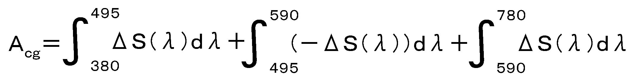
(4)
[46][44]または[45]に記載の発光装置であって、
前記発光装置から当該放射方向に出射される光が以下の(1)及び(2)を満たすことを特徴とする発光装置。
(1)前記発光装置から当該放射方向に出射される光による照明を数学的に仮定した場合の#01から#15の下記15種類の修正マンセル色票のCIE 1976 L*a*b*色空間におけるa*値、b*値をそれぞれa* nSSL、b* nSSL(ただしnは1から15の自然数)とし、
当該放射方向に出射される光の相関色温度TSSL(K)に応じて選択される基準の光での照明を数学的に仮定した場合の当該15種類の修正マンセル色票のCIE 1976 L*a*b*色空間におけるa*値、b*値をそれぞれa* nref、b* nref(ただしnは1から15の自然数)とした場合に、飽和度差ΔCnが
-3.8 ≦ ΔCn ≦ 18.6 (nは1から15の自然数)
を満たし、下記式(1)で表される飽和度差の平均が下記式(2)を満たし、

(1)
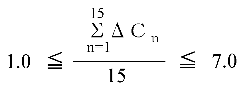
(2)
かつ飽和度差の最大値をΔCmax、飽和度差の最小値をΔCminとした場合に、飽和度差の最大値と、飽和度差の最小値との間の差ΔCmax-ΔCminが
2.8 ≦ (ΔCmax-ΔCmin) ≦ 19.6
を満たす。
ただし、ΔCn=√{(a* nSSL)2+(b* nSSL)2}-√{(a* nref)2+(b* nref)2}とする。
15種類の修正マンセル色票
#01 7.5 P 4 /10
#02 10 PB 4 /10
#03 5 PB 4 /12
#04 7.5 B 5 /10
#05 10 BG 6 / 8
#06 2.5 BG 6 /10
#07 2.5 G 6 /12
#08 7.5 GY 7 /10
#09 2.5 GY 8 /10
#10 5 Y 8.5/12
#11 10 YR 7 /12
#12 5 YR 7 /12
#13 10 R 6 /12
#14 5 R 4 /14
#15 7.5 RP 4 /12
(2)前記発光装置から当該放射方向に出射される光による照明を数学的に仮定した場合の上記15種類の修正マンセル色票のCIE 1976 L*a*b*色空間における色相角をθnSSL(度)(ただしnは1から15の自然数)とし、
当該放射方向に出射される光の相関色温度TSSL(K)に応じて選択される基準の光での照明を数学的に仮定した場合の当該15種類の修正マンセル色票のCIE 1976 L*a*b*色空間における色相角をθnref(度)(ただしnは1から15の自然数)とした場合に、色相角差の絶対値|Δhn|が
0 ≦ |Δhn| ≦ 9.0(度)(nは1から15の自然数)
を満たす。
ただし、Δhn=θnSSL-θnrefとする。
[47][44]~[46]のいずれかに記載の発光装置であって、
前記発光装置から当該放射方向に出射される光は、分光分布φSSL(λ)から導出される波長380nm以上780nm以下の範囲の放射効率K(lm/W)が
180(lm/W) ≦ K(lm/W) ≦ 320(lm/W)
を満たすことを特徴とする発光装置。
[48][46]に記載の発光装置であって、前記色相角差の絶対値|Δhn|が
0.003 ≦ |Δhn| ≦ 8.3(度)(nは1から15の自然数)
を満たすことを特徴とする発光装置。
[49][46]に記載の発光装置であって、前記一般式(1)で表される飽和度差の平均が下記式(2)´
を満たすことを特徴とする発光装置。

(2)´
[50][46]に記載の発光装置であって、前記飽和度差ΔCnが
-3.4 ≦ ΔCn ≦ 16.8 (nは1から15の自然数)
を満たすことを特徴とする発光装置。
[51][46]に記載の発光装置であって、前記飽和度差の最大値と、前記飽和度差の最小値との間の差ΔCmax-ΔCminが
3.2 ≦ (ΔCmax-ΔCmin) ≦ 17.8
を満たすことを特徴とする発光装置。
[52][44]~[51]のいずれかに記載の発光装置であって、
前記発光装置から当該放射方向に出射される光は、黒体放射軌跡からの距離DUVSSLが
-0.0250 ≦ DuvSSL ≦ -0.0100
を満たすことを特徴とする発光装置。
[53][44]~[52]のいずれかに記載の発光装置であって、前記数式(3)または(4)で表される指標Acgが
-322 ≦ Acg ≦ -12
を満たすことを特徴とする発光装置。
[54][44]~[53]のいずれかに記載の発光装置であって、
前記発光装置から当該放射方向に出射される光は、分光分布φSSL(λ)から導出される波長380nm以上780nm以下の範囲の放射効率K(lm/W)が、
206(lm/W) ≦ K(lm/W) ≦ 288(lm/W)
を満たすことを特徴とする発光装置。
[55][44]~[54]のいずれかに記載の発光装置であって、前記相関色温度TSSL(K)が
2550(K) ≦ TSSL(K) ≦ 5650(K)
を満たすことを特徴とする発光装置。
[56][44]~[55]のいずれかに記載の発光装置であって、前記発光装置から当該放射方向に出射される光が対象物を照明する照度が150lx以上5000lx以下であることを特徴とする発光装置。
[57][44]~[56]のいずれかに記載の発光装置であって、前記発光装置は、前記半導体発光素子が出射する光を含めて1種類以上6種類以下の発光要素から出射される光を当該放射方向に発することを特徴とする発光装置。
[58][44]~[57]のいずれかに記載の発光装置であって、前記半導体発光素子の発光スペクトルのピーク波長が380nm以上495nm未満であって、かつ、半値全幅が2nm以上45nm以下であることを特徴とする発光装置。
[59][58]に記載の発光装置であって、前記半導体発光素子の発光スペクトルのピーク波長が395nm以上420nm未満であることを特徴とする発光装置。
[60][58]に記載の発光装置であって、前記半導体発光素子の発光スペクトルのピーク波長が420nm以上455nm未満であることを特徴とする発光装置。
[61][58]に記載の発光装置であって、当該半導体発光素子の発光スペクトルのピーク波長が455nm以上485nm未満であることを特徴とする発光装置。
[62][44]~[57]のいずれかに記載の発光装置であって、前記半導体発光素子の発光スペクトルのピーク波長が495nm以上590nm未満であって、かつ、半値全幅が2nm以上75nm以下であることを特徴とする発光装置。
[63][44]~[57]のいずれかに記載の発光装置であって、前記半導体発光素子の発光スペクトルのピーク波長が590nm以上780nm未満であって、かつ、半値全幅が2nm以上30nm以下であることを特徴とする発光装置。
[64][44]~[63]のいずれかに記載の発光装置であって、前記半導体発光素子はサファイア基板、GaN基板、GaAs基板、GaP基板からなる群から選択されるいずれかの基板上で作成されたことを特徴とする発光装置。
[65][44]~[63]のいずれかに記載の発光装置であって、前記半導体発光素子はGaN基板、またはGaP基板上で作成され、かつ前記基板の厚みが100μm以上2mm以下であることを特徴とする発光装置。
[66][44]~[63]のいずれかに記載の発光装置であって、前記半導体発光素子はサファイア基板、またはGaAs基板上で作成され、かつ半導体発光素子は基板から剥離されてなることを特徴とする発光装置。
[67][44]~[66]のいずれかに記載の発光装置であって、発光要素として蛍光体を備えることを特徴とする発光装置。
[68][67]に記載の発光装置であって、前記蛍光体は、発光スペクトルの異なる蛍光体を1種類以上5種類以下含むことを特徴とする発光装置。
[69][67]または[68]に記載の発光装置であって、前記蛍光体は、室温で光励起した場合の単体発光スペクトルのピーク波長が380nm以上495nm未満であって、かつ、半値全幅が2nm以上90nm以下である蛍光体を含むことを特徴とする発光装置。
[70][69]に記載の発光装置であって、前記蛍光体が下記一般式(5)で表される蛍光体、下記一般式(5)´で表される蛍光体、(Sr,Ba)3MgSi2O8:Eu2+、および(Ba,Sr,Ca,Mg)Si2O2N2:Euからなる群から選択される1種以上を含むことを特徴とする発光装置。
(Ba、Sr、Ca)MgAl10O17:Mn,Eu (5)
SraBabEux(PO4)cXd (5)´
(一般式(5)´において、XはClである。また、c、d及びxは、2.7≦c≦3.3、0.9≦d≦1.1、0.3≦x≦1.2を満足する数である。さらに、a及びbは、a+b=5-xかつ0≦b/(a+b)≦0.6の条件を満足する。)
[71][67]または[68]に記載の発光装置であって、前記蛍光体は、室温で光励起した場合の単体発光スペクトルのピーク波長が495nm以上590nm未満であって、かつ、半値全幅が2nm以上130nm以下である蛍光体を含むことを特徴とする発光装置。
[72][71]に記載の発光装置であって、前記蛍光体がSi6-zAlzOzN8-z:Eu(ただし0<z<4.2)、下記一般式(6)で表される蛍光体、下記一般式(6)´で表される蛍光体、およびSrGaS4:Eu2+からなる群から選択される1種以上を含むことを特徴とする発光装置。
(BaaCabSrcMgdEux)SiO4 (6)
(一般式(6)においてa、b、c、dおよびxが、a+b+c+d+x=2、1.0 ≦ a ≦ 2.0、0 ≦ b < 0.2、0.2 ≦ c ≦ 0.8、0 ≦ d < 0.2および0 < x ≦ 0.5を満たす。)
Ba1-x-y SrxEuy Mg1-z Mnz Al10O17 (6)´
(一般式(6)´においてx、yおよびzはそれぞれ0.1≦x≦0.4、0.25≦y≦0.6及び0.05≦z≦0.5を満たす。)
[73][67]または[68]に記載の発光装置であって、前記蛍光体は、室温で光励起した場合の単体発光スペクトルのピーク波長が590nm以上780nm未満であって、かつ、半値全幅が2nm以上130nm以下である蛍光体を含むことを特徴とする発光装置。
[74][73]に記載の発光装置であって、前記蛍光体が下記一般式(7)で表される蛍光体、下記一般式(7)´で表される蛍光体、(Sr,Ca,Ba)2AlxSi5-xOxN8-x:Eu(ただし0≦x≦2)、Euy(Sr,Ca,Ba)1-y:Al1+xSi4-xOxN7-x(ただし0≦x<4、0≦y<0.2)、K2SiF6:Mn4+、A2+xMyMnzFn(AはNaおよび/またはK;MはSiおよびAl;-1≦x≦1かつ0.9≦y+z≦1.1かつ0.001≦z≦0.4かつ5≦n≦7)、(Ca,Sr,Ba,Mg)AlSiN3:Euおよび/または(Ca,Sr,Ba)AlSiN3:Eu、並びに(CaAlSiN3)1-x(Si2N2O)x:Eu(ただし、xは0<x<0.5)からなる群から選択される1種以上を含むことを特徴とする発光装置。
(La1-x-y,Eux,Lny)2O2S (7)
(一般式(7)において、x及びyはそれぞれ0.02≦x≦0.50及び0≦y≦0.50を満たす数を表し、LnはY、Gd、Lu、Sc、Sm及びErの少なくとも1種の3価希土類元素を表す。)
(k-x)MgO・xAF2・GeO2:yMn4+ (7)´
(一般式(7)´において、k、x、yは、各々、2.8≦k≦5、0.1≦x≦0.7、0.005≦y≦0.015を満たす数を表し、Aはカルシウム(Ca)、ストロンチウム(Sr)、バリウム(Ba)、亜鉛(Zn)、またはこれらの混合物である。)
[75][44]~[57]のいずれかに記載の発光装置であって、発光要素として蛍光体を備え、前記半導体発光素子は発光スペクトルのピーク波長が395nm以上420nm未満であり、前記蛍光体は、SBCA、β-SiAlON、およびCASONを含むことを特徴とする発光装置。
[76][44]~[57]のいずれかに記載の発光装置であって、発光要素として蛍光体を備え、前記半導体発光素子は発光スペクトルのピーク波長が395nm以上420nm未満であり、前記蛍光体は、SCA、β-SiAlON、およびCASONを含むことを特徴とする発光装置。
[77][44]~[76]のいずれかに記載の発光装置であって、パッケージ化LED、LEDモジュール、LED照明器具、およびLED照明システムからなる群から選択されるいずれかであることを特徴とする発光装置。
[78]家庭用照明装置として用いられる、[44]~[77]のいずれかに記載の発光装置。
[79]展示物用照明装置として用いられる、[44]~[77]のいずれかに記載の発光装置。
[80]演出用照明装置として用いられる、[44]~[77]のいずれかに記載の発光装置。
[81]医療用照明装置として用いられる、[44]~[77]のいずれかに記載の発光装置。
[82]作業用照明装置として用いられる、[44]~[77]のいずれかに記載の発光装置。
[83]工業機器内用照明装置として用いられる、[44]~[77]のいずれかに記載の発光装置。
[84]交通機関内装用照明装置として用いられる、[44]~[77]のいずれかに記載の発光装置。
[85]美術品用照明装置として用いられる、[44]~[77]のいずれかに記載の発光装置。
[86]高齢者用照明装置として用いられる、[44]~[77]のいずれかに記載の発光装置。
また、上記目的を達成するための本発明の第三の実施態様は以下の事項に関する。
[87]少なくとも半導体発光素子を発光要素として備える発光装置の設計方法であって、
前記発光装置から出射される光が、ANSI C78.377で定義される黒体放射軌跡からの距離DUVSSLが-0.0350 ≦ DuvSSL ≦ -0.0040である光を、主たる放射方向に含むようにし、
かつ、
前記発光装置から当該放射方向に出射される光の分光分布をφSSL(λ)、前記発光装置から当該放射方向に出射される光のTSSL(K)に応じて選択される基準の光の分光分布をφref(λ)、前記発光装置から当該放射方向に出射される光の三刺激値を(XSSL、YSSL、ZSSL)、前記発光装置から当該放射方向に出射される光のTSSL(K)に応じて選択される基準の光の三刺激値を(Xref、Yref、Zref)とし、
前記発光装置から当該放射方向に出射される光の規格化分光分布SSSL(λ)と、前記発光装置から当該放射方向に出射される光のTSSL(K)に応じて選択される基準の光の規格化分光分布Sref(λ)と、これら規格化分光分布の差ΔS(λ)をそれぞれ、
SSSL(λ)=φSSL(λ)/YSSL
Sref(λ)=φref(λ)/Yref
ΔS(λ)=Sref(λ)-SSSL(λ)
と定義し、
波長380nm以上780nm以内の範囲で、SSSL(λ)の最長波長極大値を与える波長をλR(nm)とした際に、λRよりも長波長側にSSSL(λR)/2となる波長Λ4が存在し、
下記数式(3)で表される指標Acgが、-360 ≦ Acg ≦ -10となるように調整することを特徴とする発光装置の設計方法。

(3)
[88]少なくとも半導体発光素子を発光要素として備える発光装置の設計方法であって、
前記発光装置から出射される光が、ANSI C78.377で定義される黒体放射軌跡からの距離DUVSSLが-0.0350 ≦ DuvSSL ≦ -0.0040である光を、主たる放射方向に含むようにし、
かつ、
前記発光装置から当該放射方向に出射される光の分光分布をφSSL(λ)、前記発光装置から当該放射方向に出射される光のTSSL(K)に応じて選択される基準の光の分光分布をφref(λ)、前記発光装置から当該放射方向に出射される光の三刺激値を(XSSL、YSSL、ZSSL)、前記発光装置から当該放射方向に出射される光のTSSL(K)に応じて選択される基準の光の三刺激値を(Xref、Yref、Zref)とし、
前記発光装置から当該放射方向に出射される光の規格化分光分布SSSL(λ)と、前記発光装置から当該放射方向に出射される光のTSSL(K)に応じて選択される基準の光の規格化分光分布Sref(λ)と、これら規格化分光分布の差ΔS(λ)をそれぞれ、
SSSL(λ)=φSSL(λ)/YSSL
Sref(λ)=φref(λ)/Yref
ΔS(λ)=Sref(λ)-SSSL(λ)
と定義し、
波長380nm以上780nm以内の範囲で、SSSL(λ)の最長波長極大値を与える波長をλR(nm)とした際に、λRよりも長波長側にSSSL(λR)/2となる波長Λ4が存在せず、
下記数式(4)で表される指標Acgが、-360 ≦ Acg ≦ -10となるように調整することを特徴とする発光装置の設計方法。

(4)
[1]照明対象物を準備する照明対象物準備工程、および、発光要素である半導体発光素子を含む発光装置から出射される光により対象物を照明する照明工程、を含む照明方法であって、
前記照明工程において、前記発光装置から出射される光が対象物を照明した際に、前記対象物の位置で測定した光が以下の(1)、(2)及び(3)を満たすように照明することを特徴とする照明方法。
(1)前記対象物の位置で測定した光のANSI C78.377で定義される黒体放射軌跡からの距離DUVSSLが、-0.0350 ≦ DuvSSL ≦ -0.0040である。
(2)前記対象物の位置で測定した光による照明を数学的に仮定した場合の#01から#15の下記15種類の修正マンセル色票のCIE 1976 L*a*b*色空間におけるa*値、b*値をそれぞれa* nSSL、b* nSSL(ただしnは1から15の自然数)とし、
前記対象物の位置で測定した光の相関色温度TSSL(K)に応じて選択される基準の光による照明を数学的に仮定した場合の当該15種類の修正マンセル色票のCIE 1976 L*a*b*色空間におけるa*値、b*値をそれぞれa* nref、b* nref(ただしnは1から15の自然数)とした場合に、飽和度差ΔCnが
-3.8 ≦ ΔCn ≦ 18.6 (nは1から15の自然数)
を満たし、
下記式(1)で表される飽和度差の平均が下記式(2)を満たし、
かつ、飽和度差の最大値をΔCmax、飽和度差の最小値をΔCminとした場合に、飽和度差の最大値と、飽和度差の最小値との間の差ΔCmax-ΔCminが
2.8 ≦ (ΔCmax-ΔCmin) ≦ 19.6
を満たす。
ただし、ΔCn=√{(a* nSSL)2+(b* nSSL)2}-√{(a* nref)2+(b* nref)2}とする。
15種類の修正マンセル色票
#01 7.5 P 4 /10
#02 10 PB 4 /10
#03 5 PB 4 /12
#04 7.5 B 5 /10
#05 10 BG 6 / 8
#06 2.5 BG 6 /10
#07 2.5 G 6 /12
#08 7.5 GY 7 /10
#09 2.5 GY 8 /10
#10 5 Y 8.5/12
#11 10 YR 7 /12
#12 5 YR 7 /12
#13 10 R 6 /12
#14 5 R 4 /14
#15 7.5 RP 4 /12
(3)前記対象物の位置で測定した光による照明を数学的に仮定した場合の上記15種類の修正マンセル色票のCIE 1976 L*a*b*色空間における色相角をθnSSL(度)(ただしnは1から15の自然数)とし、
前記対象物の位置で測定した光の相関色温度TSSL(K)に応じて選択される基準の光による照明を数学的に仮定した場合の当該15種類の修正マンセル色票のCIE 1976 L*a*b*色空間における色相角をθnref(度)(ただしnは1から15の自然数)とした場合に、色相角差の絶対値|Δhn|が
0 ≦ |Δhn| ≦ 9.0(度)(nは1から15の自然数)
を満たす。
ただし、Δhn=θnSSL-θnrefとする。
[2][1]に記載の照明方法であって、
前記対象物の位置で測定した光の分光分布をφSSL(λ)、前記対象物の位置で測定した光のTSSL(K)に応じて選択される基準の光の分光分布をφref(λ)、前記対象物の位置で測定した光の三刺激値を(XSSL、YSSL、ZSSL)、前記対象物の位置で測定した光のTSSL(K)に応じて選択される基準の光の三刺激値を(Xref、Yref、Zref)とし、
前記対象物の位置で測定した光の規格化分光分布SSSL(λ)と、前記対象物の位置で測定した光のTSSL(K)に応じて選択される基準の光の規格化分光分布Sref(λ)と、これら規格化分光分布の差ΔS(λ)をそれぞれ、
SSSL(λ)=φSSL(λ)/YSSL
Sref(λ)=φref(λ)/Yref
ΔS(λ)=Sref(λ)-SSSL(λ)
と定義し、
波長380nm以上780nm以内の範囲で、SSSL(λ)の最長波長極大値を与える波長をλR(nm)とした際に、λRよりも長波長側にSSSL(λR)/2となる波長Λ4が存在し、
前記対象物の位置で測定した光の下記数式(3)で表される指標Acgが、-360 ≦ Acg ≦ -10を満たすことを特徴とする照明方法。
[3][1]に記載の照明方法であって、
前記対象物の位置で測定した光の分光分布をφSSL(λ)、前記対象物の位置で測定した光のTSSL(K)に応じて選択される基準の光の分光分布をφref(λ)、前記対象物の位置で測定した光の三刺激値を(XSSL、YSSL、ZSSL)、前記対象物の位置で測定した光のTSSL(K)に応じて選択される基準の光の三刺激値を(Xref、Yref、Zref)とし、
前記対象物の位置で測定した光の規格化分光分布SSSL(λ)と、前記対象物の位置で測定した光のTSSL(K)に応じて選択される基準の光の規格化分光分布Sref(λ)と、これら規格化分光分布の差ΔS(λ)をそれぞれ、
SSSL(λ)=φSSL(λ)/YSSL
Sref(λ)=φref(λ)/Yref
ΔS(λ)=Sref(λ)-SSSL(λ)
と定義し、
波長380nm以上780nm以内の範囲で、SSSL(λ)の最長波長極大値を与える波長をλR(nm)とした際に、λRよりも長波長側にSSSL(λR)/2となる波長Λ4が存在せず、
前記対象物の位置で測定した光の下記数式(4)で表される指標Acgが、-360 ≦ Acg ≦ -10を満たすことを特徴とする照明方法。
[4][1]~[3]のいずれかに記載の照明方法であって、
前記対象物の位置で測定した光の分光分布φSSL(λ)から導出される波長380nm以上780nm以下の範囲の放射効率K(lm/W)が
180(lm/W) ≦ K(lm/W) ≦ 320(lm/W)
を満たすことを特徴とする照明方法。
[5][1]~[4]のいずれかに記載の照明方法であって、前記色相角差の絶対値|Δhn|が
0.003 ≦ |Δhn| ≦ 8.3(度)(nは1から15の自然数)
を満たすことを特徴とする照明方法。
[6][1]~[5]のいずれかに記載の照明方法であって、前記一般式(1)で表される飽和度差の平均が下記式(2)´
を満たすことを特徴とする照明方法。
[7][1]~[6]のいずれかに記載の照明方法であって、前記飽和度差ΔCnが
-3.4 ≦ ΔCn ≦ 16.8 (nは1から15の自然数)
を満たすことを特徴とする照明方法。
[8][1]~[7]のいずれかに記載の照明方法であって、前記飽和度差の最大値と、前記飽和度差の最小値との間の差ΔCmax-ΔCminが
3.2 ≦ (ΔCmax-ΔCmin) ≦ 17.8
を満たすことを特徴とする照明方法。
[9][1]~[8]のいずれかに記載の照明方法であって、
前記対象物の位置で測定した光は、黒体放射軌跡からの距離DUVSSLが
-0.0250 ≦ DuvSSL ≦ -0.0100
を満たすことを特徴とする照明方法。
[10][2]または[3]に記載の照明方法であって、前記数式(3)または(4)で表される指標Acgが
-322 ≦ Acg ≦ -12
を満たすことを特徴とする照明方法。
[11][1]~[10]のいずれかに記載の照明方法であって、
前記対象物の位置で測定した光は、分光分布φSSL(λ)から導出される波長380nm以上780nm以下の範囲の放射効率K(lm/W)が
206(lm/W) ≦ K(lm/W) ≦ 288(lm/W)
を満たすことを特徴とする照明方法。
[12][1]~[11]のいずれかに記載の照明方法であって、前記対象物の位置で測定した光の相関色温度TSSL(K)が
2550(K) ≦ TSSL(K) ≦ 5650(K)
を満たすことを特徴とする照明方法。
[13][1]~[12]のいずれかに記載の照明方法であって、前記対象物を照明する照度が150lx以上5000lx以下であることを特徴とする照明方法。
[14][1]~[13]のいずれかに記載の照明方法であって、前記発光装置は、前記半導体発光素子が出射する光を含めて1種類以上6種類以下の発光要素から出射される光を発することを特徴とする照明方法。
[15][1]~[14]のいずれかに記載の照明方法であって、前記半導体発光素子の発光スペクトルのピーク波長が380nm以上495nm未満であって、かつ、半値全幅が2nm以上45nm以下であることを特徴とする照明方法。
[16][15]に記載の照明方法であって、前記半導体発光素子の発光スペクトルのピーク波長が395nm以上420nm未満であることを特徴とする照明方法。
[17][15]に記載の照明方法であって、前記半導体発光素子の発光スペクトルのピーク波長が420nm以上455nm未満であることを特徴とする照明方法。
[18][15]に記載の照明方法であって、当該半導体発光素子の発光スペクトルのピーク波長が455nm以上485nm未満であることを特徴とする照明方法。
[19][1]~[14]のいずれかに記載の照明方法であって、前記半導体発光素子の発光スペクトルのピーク波長が495nm以上590nm未満であって、かつ、半値全幅が2nm以上75nm以下であることを特徴とする照明方法。
[20][1]~[14]のいずれかに記載の照明方法であって、前記半導体発光素子の発光スペクトルのピーク波長が590nm以上780nm未満であって、かつ、半値全幅が2nm以上30nm以下であることを特徴とする照明方法。
[21][1]~[20]のいずれかに記載の照明方法であって、前記半導体発光素子はサファイア基板、GaN基板、GaAs基板、GaP基板からなる群から選択されるいずれかの基板上で作成されたことを特徴とする照明方法。
[22][1]~[20]のいずれかに記載の照明方法であって、前記半導体発光素子はGaN基板、またはGaP基板上で作成され、かつ前記基板の厚みが100μm以上2mm以下であることを特徴とする照明方法。
[23][1]~[20]のいずれかに記載の照明方法であって、前記半導体発光素子はサファイア基板、またはGaAs基板上で作成され、かつ半導体発光素子は基板から剥離されてなることを特徴とする照明方法。
[24][1]~[23]のいずれかに記載の照明方法であって、発光要素として蛍光体を備えることを特徴とする照明方法。
[25][24]に記載の照明方法であって、前記蛍光体は、発光スペクトルの異なる蛍光体を1種類以上5種類以下含むことを特徴とする照明方法。
[26][24]または[25]に記載の照明方法であって、前記蛍光体は、室温で光励起した場合の単体発光スペクトルのピーク波長が380nm以上495nm未満であって、かつ、半値全幅が2nm以上90nm以下である蛍光体を含むことを特徴とする照明方法。
[27][26]に記載の照明方法であって、前記蛍光体が下記一般式(5)で表される蛍光体、下記一般式(5)´で表される蛍光体、(Sr,Ba)3MgSi2O8:Eu2+、および(Ba,Sr,Ca,Mg)Si2O2N2:Euからなる群から選択される1種以上を含むことを特徴とする照明方法。
(Ba、Sr、Ca)MgAl10O17:Mn,Eu (5)
SraBabEux(PO4)cXd (5)´
(一般式(5)´において、XはClである。また、c、d及びxは、2.7≦c≦3.3、0.9≦d≦1.1、0.3≦x≦1.2を満足する数である。さらに、a及びbは、a+b=5-xかつ0≦b/(a+b)≦0.6の条件を満足する。)
[28][24]または[25]に記載の照明方法であって、前記蛍光体は、室温で光励起した場合の単体発光スペクトルのピーク波長が495nm以上590nm未満であって、かつ、半値全幅が2nm以上130nm以下である蛍光体を含むことを特徴とする照明方法。
[29][28]に記載の照明方法であって、前記蛍光体がSi6-zAlzOzN8-z:Eu(ただし0<z<4.2)、下記一般式(6)で表される蛍光体、下記一般式(6)´で表される蛍光体、およびSrGaS4:Eu2+からなる群から選択される1種以上を含むことを特徴とする照明方法。
(BaaCabSrcMgdEux)SiO4 (6)
(一般式(6)においてa、b、c、dおよびxが、a+b+c+d+x=2、1.0 ≦ a ≦ 2.0、0 ≦ b < 0.2、0.2 ≦ c ≦ 0.8、0 ≦ d < 0.2および0 < x ≦ 0.5を満たす。)
Ba1-x-y SrxEuy Mg1-z Mnz Al10O17 (6)´
(一般式(6)´においてx、yおよびzはそれぞれ0.1≦x≦0.4、0.25≦y≦0.6及び0.05≦z≦0.5を満たす。)
[30][24]または[25]に記載の照明方法であって、前記蛍光体は、室温で光励起した場合の単体発光スペクトルのピーク波長が590nm以上780nm未満であって、かつ、半値全幅が2nm以上130nm以下である蛍光体を含むことを特徴とする照明方法。
[31][30]に記載の照明方法であって、前記蛍光体が下記一般式(7)で表される蛍光体、下記一般式(7)´で表される蛍光体、(Sr,Ca,Ba)2AlxSi5-xOxN8-x:Eu(ただし0≦x≦2)、Euy(Sr,Ca,Ba)1-y:Al1+xSi4-xOxN7-x(ただし0≦x<4、0≦y<0.2)、K2SiF6:Mn4+、A2+xMyMnzFn(AはNaおよび/またはK;MはSiおよびAl;-1≦x≦1かつ0.9≦y+z≦1.1かつ0.001≦z≦0.4かつ5≦n≦7)、(Ca,Sr,Ba,Mg)AlSiN3:Euおよび/または(Ca,Sr,Ba)AlSiN3:Eu、並びに(CaAlSiN3)1-x(Si2N2O)x:Eu(ただし、xは0<x<0.5)からなる群から選択される1種以上を含むことを特徴とする照明方法。
(La1-x-y,Eux,Lny)2O2S (7)
(一般式(7)において、x及びyはそれぞれ0.02≦x≦0.50及び0≦y≦0.50を満たす数を表し、LnはY、Gd、Lu、Sc、Sm及びErの少なくとも1種の3価希土類元素を表す。)
(k-x)MgO・xAF2・GeO2:yMn4+ (7)´
(一般式(7)´において、k、x、yは、各々、2.8≦k≦5、0.1≦x≦0.7、0.005≦y≦0.015を満たす数を表し、Aはカルシウム(Ca)、ストロンチウム(Sr)、バリウム(Ba)、亜鉛(Zn)、またはこれらの混合物である。)
[32][1]~[14]のいずれかに記載の照明方法であって、発光要素として蛍光体を備え、前記半導体発光素子は発光スペクトルのピーク波長が395nm以上420nm未満であり、前記蛍光体は、SBCA、β-SiAlON、およびCASONを含むことを特徴とする照明方法。
[33][1]~[14]のいずれかに記載の照明方法であって、発光要素として蛍光体を備え、前記半導体発光素子は発光スペクトルのピーク波長が395nm以上420nm未満であり、前記蛍光体は、SCA、β-SiAlON、およびCASONを含むことを特徴とする照明方法。
[34][1]~[33]のいずれかに記載の照明方法であって、前記発光装置はパッケージ化LED、LEDモジュール、LED照明器具、およびLED照明システムからなる群から選択されるいずれかであることを特徴とする照明方法。
[35]家庭用に用いられる、[1]~[34]のいずれかに記載の照明方法。
[36]展示用に用いられる、[1]~[34]のいずれかに記載の照明方法。
[37]演出用に用いられる、[1]~[34]のいずれかに記載の照明方法。
[38]医療用に用いられる、[1]~[34]のいずれかに記載の照明方法。
[39]作業用に用いられる、[1]~[34]のいずれかに記載の照明方法。
[40]工業機器内用に用いられる、[1]~[34]のいずれかに記載の照明方法。
[41]交通機関内装用に用いられる、[1]~[34]のいずれかに記載の照明方法。
[42]美術品用に用いられる、[1]~[34]のいずれかに記載の照明方法。
[43]高齢者用に用いられる、[1]~[34]のいずれかに記載の照明方法。
また、上記目的を達成するための本発明の第二の実施態様は以下の事項に関する。
[44]少なくとも半導体発光素子を発光要素として備える発光装置であって、
前記発光装置から出射される光は、ANSI C78.377で定義される黒体放射軌跡からの距離DUVSSLが、-0.0350 ≦ DuvSSL ≦ -0.0040となる光を主たる放射方向に含み、
かつ、
前記発光装置から当該放射方向に出射される光の分光分布をφSSL(λ)、前記発光装置から当該放射方向に出射される光のTSSL(K)に応じて選択される基準の光の分光分布をφref(λ)、前記発光装置から当該放射方向に出射される光の三刺激値を(XSSL、YSSL、ZSSL)、前記発光装置から当該放射方向に出射される光のTSSL(K)に応じて選択される基準の光の三刺激値を(Xref、Yref、Zref)とし、
前記発光装置から当該放射方向に出射される光の規格化分光分布SSSL(λ)と、前記発光装置から当該放射方向に出射される光のTSSL(K)に応じて選択される基準の光の規格化分光分布Sref(λ)と、これら規格化分光分布の差ΔS(λ)をそれぞれ、
SSSL(λ)=φSSL(λ)/YSSL
Sref(λ)=φref(λ)/Yref
ΔS(λ)=Sref(λ)-SSSL(λ)
と定義し、
波長380nm以上780nm以内の範囲で、SSSL(λ)の最長波長極大値を与える波長をλR(nm)とした際に、λRよりも長波長側にSSSL(λR)/2となる波長Λ4が存在し、
下記数式(3)で表される指標Acgが、-360 ≦ Acg ≦ -10を満たすことを特徴とする発光装置。
[45]少なくとも半導体発光素子を発光要素として備える発光装置であって、
前記発光装置から出射される光は、ANSI C78.377で定義される黒体放射軌跡からの距離DUVSSLが、-0.0350 ≦ DuvSSL ≦ -0.0040となる光を主たる放射方向に含み、
かつ、
前記発光装置から当該放射方向に出射される光の分光分布をφSSL(λ)、前記発光装置から当該放射方向に出射される光のTSSL(K)に応じて選択される基準の光の分光分布をφref(λ)、前記発光装置から当該放射方向に出射される光の三刺激値を(XSSL、YSSL、ZSSL)、前記発光装置から当該放射方向に出射される光のTSSL(K)に応じて選択される基準の光の三刺激値を(Xref、Yref、Zref)とし、
前記発光装置から当該放射方向に出射される光の規格化分光分布SSSL(λ)と、前記発光装置から当該放射方向に出射される光のTSSL(K)に応じて選択される基準の光の規格化分光分布Sref(λ)と、これら規格化分光分布の差ΔS(λ)をそれぞれ、
SSSL(λ)=φSSL(λ)/YSSL
Sref(λ)=φref(λ)/Yref
ΔS(λ)=Sref(λ)-SSSL(λ)
と定義し、
波長380nm以上780nm以内の範囲で、SSSL(λ)の最長波長極大値を与える波長をλR(nm)とした際に、λRよりも長波長側にSSSL(λR)/2となる波長Λ4が存在せず、
下記数式(4)で表される指標Acgが、-360 ≦ Acg ≦ -10を満たすことを特徴とする発光装置。
[46][44]または[45]に記載の発光装置であって、
前記発光装置から当該放射方向に出射される光が以下の(1)及び(2)を満たすことを特徴とする発光装置。
(1)前記発光装置から当該放射方向に出射される光による照明を数学的に仮定した場合の#01から#15の下記15種類の修正マンセル色票のCIE 1976 L*a*b*色空間におけるa*値、b*値をそれぞれa* nSSL、b* nSSL(ただしnは1から15の自然数)とし、
当該放射方向に出射される光の相関色温度TSSL(K)に応じて選択される基準の光での照明を数学的に仮定した場合の当該15種類の修正マンセル色票のCIE 1976 L*a*b*色空間におけるa*値、b*値をそれぞれa* nref、b* nref(ただしnは1から15の自然数)とした場合に、飽和度差ΔCnが
-3.8 ≦ ΔCn ≦ 18.6 (nは1から15の自然数)
を満たし、下記式(1)で表される飽和度差の平均が下記式(2)を満たし、
かつ飽和度差の最大値をΔCmax、飽和度差の最小値をΔCminとした場合に、飽和度差の最大値と、飽和度差の最小値との間の差ΔCmax-ΔCminが
2.8 ≦ (ΔCmax-ΔCmin) ≦ 19.6
を満たす。
ただし、ΔCn=√{(a* nSSL)2+(b* nSSL)2}-√{(a* nref)2+(b* nref)2}とする。
15種類の修正マンセル色票
#01 7.5 P 4 /10
#02 10 PB 4 /10
#03 5 PB 4 /12
#04 7.5 B 5 /10
#05 10 BG 6 / 8
#06 2.5 BG 6 /10
#07 2.5 G 6 /12
#08 7.5 GY 7 /10
#09 2.5 GY 8 /10
#10 5 Y 8.5/12
#11 10 YR 7 /12
#12 5 YR 7 /12
#13 10 R 6 /12
#14 5 R 4 /14
#15 7.5 RP 4 /12
(2)前記発光装置から当該放射方向に出射される光による照明を数学的に仮定した場合の上記15種類の修正マンセル色票のCIE 1976 L*a*b*色空間における色相角をθnSSL(度)(ただしnは1から15の自然数)とし、
当該放射方向に出射される光の相関色温度TSSL(K)に応じて選択される基準の光での照明を数学的に仮定した場合の当該15種類の修正マンセル色票のCIE 1976 L*a*b*色空間における色相角をθnref(度)(ただしnは1から15の自然数)とした場合に、色相角差の絶対値|Δhn|が
0 ≦ |Δhn| ≦ 9.0(度)(nは1から15の自然数)
を満たす。
ただし、Δhn=θnSSL-θnrefとする。
[47][44]~[46]のいずれかに記載の発光装置であって、
前記発光装置から当該放射方向に出射される光は、分光分布φSSL(λ)から導出される波長380nm以上780nm以下の範囲の放射効率K(lm/W)が
180(lm/W) ≦ K(lm/W) ≦ 320(lm/W)
を満たすことを特徴とする発光装置。
[48][46]に記載の発光装置であって、前記色相角差の絶対値|Δhn|が
0.003 ≦ |Δhn| ≦ 8.3(度)(nは1から15の自然数)
を満たすことを特徴とする発光装置。
[49][46]に記載の発光装置であって、前記一般式(1)で表される飽和度差の平均が下記式(2)´
を満たすことを特徴とする発光装置。
[50][46]に記載の発光装置であって、前記飽和度差ΔCnが
-3.4 ≦ ΔCn ≦ 16.8 (nは1から15の自然数)
を満たすことを特徴とする発光装置。
[51][46]に記載の発光装置であって、前記飽和度差の最大値と、前記飽和度差の最小値との間の差ΔCmax-ΔCminが
3.2 ≦ (ΔCmax-ΔCmin) ≦ 17.8
を満たすことを特徴とする発光装置。
[52][44]~[51]のいずれかに記載の発光装置であって、
前記発光装置から当該放射方向に出射される光は、黒体放射軌跡からの距離DUVSSLが
-0.0250 ≦ DuvSSL ≦ -0.0100
を満たすことを特徴とする発光装置。
[53][44]~[52]のいずれかに記載の発光装置であって、前記数式(3)または(4)で表される指標Acgが
-322 ≦ Acg ≦ -12
を満たすことを特徴とする発光装置。
[54][44]~[53]のいずれかに記載の発光装置であって、
前記発光装置から当該放射方向に出射される光は、分光分布φSSL(λ)から導出される波長380nm以上780nm以下の範囲の放射効率K(lm/W)が、
206(lm/W) ≦ K(lm/W) ≦ 288(lm/W)
を満たすことを特徴とする発光装置。
[55][44]~[54]のいずれかに記載の発光装置であって、前記相関色温度TSSL(K)が
2550(K) ≦ TSSL(K) ≦ 5650(K)
を満たすことを特徴とする発光装置。
[56][44]~[55]のいずれかに記載の発光装置であって、前記発光装置から当該放射方向に出射される光が対象物を照明する照度が150lx以上5000lx以下であることを特徴とする発光装置。
[57][44]~[56]のいずれかに記載の発光装置であって、前記発光装置は、前記半導体発光素子が出射する光を含めて1種類以上6種類以下の発光要素から出射される光を当該放射方向に発することを特徴とする発光装置。
[58][44]~[57]のいずれかに記載の発光装置であって、前記半導体発光素子の発光スペクトルのピーク波長が380nm以上495nm未満であって、かつ、半値全幅が2nm以上45nm以下であることを特徴とする発光装置。
[59][58]に記載の発光装置であって、前記半導体発光素子の発光スペクトルのピーク波長が395nm以上420nm未満であることを特徴とする発光装置。
[60][58]に記載の発光装置であって、前記半導体発光素子の発光スペクトルのピーク波長が420nm以上455nm未満であることを特徴とする発光装置。
[61][58]に記載の発光装置であって、当該半導体発光素子の発光スペクトルのピーク波長が455nm以上485nm未満であることを特徴とする発光装置。
[62][44]~[57]のいずれかに記載の発光装置であって、前記半導体発光素子の発光スペクトルのピーク波長が495nm以上590nm未満であって、かつ、半値全幅が2nm以上75nm以下であることを特徴とする発光装置。
[63][44]~[57]のいずれかに記載の発光装置であって、前記半導体発光素子の発光スペクトルのピーク波長が590nm以上780nm未満であって、かつ、半値全幅が2nm以上30nm以下であることを特徴とする発光装置。
[64][44]~[63]のいずれかに記載の発光装置であって、前記半導体発光素子はサファイア基板、GaN基板、GaAs基板、GaP基板からなる群から選択されるいずれかの基板上で作成されたことを特徴とする発光装置。
[65][44]~[63]のいずれかに記載の発光装置であって、前記半導体発光素子はGaN基板、またはGaP基板上で作成され、かつ前記基板の厚みが100μm以上2mm以下であることを特徴とする発光装置。
[66][44]~[63]のいずれかに記載の発光装置であって、前記半導体発光素子はサファイア基板、またはGaAs基板上で作成され、かつ半導体発光素子は基板から剥離されてなることを特徴とする発光装置。
[67][44]~[66]のいずれかに記載の発光装置であって、発光要素として蛍光体を備えることを特徴とする発光装置。
[68][67]に記載の発光装置であって、前記蛍光体は、発光スペクトルの異なる蛍光体を1種類以上5種類以下含むことを特徴とする発光装置。
[69][67]または[68]に記載の発光装置であって、前記蛍光体は、室温で光励起した場合の単体発光スペクトルのピーク波長が380nm以上495nm未満であって、かつ、半値全幅が2nm以上90nm以下である蛍光体を含むことを特徴とする発光装置。
[70][69]に記載の発光装置であって、前記蛍光体が下記一般式(5)で表される蛍光体、下記一般式(5)´で表される蛍光体、(Sr,Ba)3MgSi2O8:Eu2+、および(Ba,Sr,Ca,Mg)Si2O2N2:Euからなる群から選択される1種以上を含むことを特徴とする発光装置。
(Ba、Sr、Ca)MgAl10O17:Mn,Eu (5)
SraBabEux(PO4)cXd (5)´
(一般式(5)´において、XはClである。また、c、d及びxは、2.7≦c≦3.3、0.9≦d≦1.1、0.3≦x≦1.2を満足する数である。さらに、a及びbは、a+b=5-xかつ0≦b/(a+b)≦0.6の条件を満足する。)
[71][67]または[68]に記載の発光装置であって、前記蛍光体は、室温で光励起した場合の単体発光スペクトルのピーク波長が495nm以上590nm未満であって、かつ、半値全幅が2nm以上130nm以下である蛍光体を含むことを特徴とする発光装置。
[72][71]に記載の発光装置であって、前記蛍光体がSi6-zAlzOzN8-z:Eu(ただし0<z<4.2)、下記一般式(6)で表される蛍光体、下記一般式(6)´で表される蛍光体、およびSrGaS4:Eu2+からなる群から選択される1種以上を含むことを特徴とする発光装置。
(BaaCabSrcMgdEux)SiO4 (6)
(一般式(6)においてa、b、c、dおよびxが、a+b+c+d+x=2、1.0 ≦ a ≦ 2.0、0 ≦ b < 0.2、0.2 ≦ c ≦ 0.8、0 ≦ d < 0.2および0 < x ≦ 0.5を満たす。)
Ba1-x-y SrxEuy Mg1-z Mnz Al10O17 (6)´
(一般式(6)´においてx、yおよびzはそれぞれ0.1≦x≦0.4、0.25≦y≦0.6及び0.05≦z≦0.5を満たす。)
[73][67]または[68]に記載の発光装置であって、前記蛍光体は、室温で光励起した場合の単体発光スペクトルのピーク波長が590nm以上780nm未満であって、かつ、半値全幅が2nm以上130nm以下である蛍光体を含むことを特徴とする発光装置。
[74][73]に記載の発光装置であって、前記蛍光体が下記一般式(7)で表される蛍光体、下記一般式(7)´で表される蛍光体、(Sr,Ca,Ba)2AlxSi5-xOxN8-x:Eu(ただし0≦x≦2)、Euy(Sr,Ca,Ba)1-y:Al1+xSi4-xOxN7-x(ただし0≦x<4、0≦y<0.2)、K2SiF6:Mn4+、A2+xMyMnzFn(AはNaおよび/またはK;MはSiおよびAl;-1≦x≦1かつ0.9≦y+z≦1.1かつ0.001≦z≦0.4かつ5≦n≦7)、(Ca,Sr,Ba,Mg)AlSiN3:Euおよび/または(Ca,Sr,Ba)AlSiN3:Eu、並びに(CaAlSiN3)1-x(Si2N2O)x:Eu(ただし、xは0<x<0.5)からなる群から選択される1種以上を含むことを特徴とする発光装置。
(La1-x-y,Eux,Lny)2O2S (7)
(一般式(7)において、x及びyはそれぞれ0.02≦x≦0.50及び0≦y≦0.50を満たす数を表し、LnはY、Gd、Lu、Sc、Sm及びErの少なくとも1種の3価希土類元素を表す。)
(k-x)MgO・xAF2・GeO2:yMn4+ (7)´
(一般式(7)´において、k、x、yは、各々、2.8≦k≦5、0.1≦x≦0.7、0.005≦y≦0.015を満たす数を表し、Aはカルシウム(Ca)、ストロンチウム(Sr)、バリウム(Ba)、亜鉛(Zn)、またはこれらの混合物である。)
[75][44]~[57]のいずれかに記載の発光装置であって、発光要素として蛍光体を備え、前記半導体発光素子は発光スペクトルのピーク波長が395nm以上420nm未満であり、前記蛍光体は、SBCA、β-SiAlON、およびCASONを含むことを特徴とする発光装置。
[76][44]~[57]のいずれかに記載の発光装置であって、発光要素として蛍光体を備え、前記半導体発光素子は発光スペクトルのピーク波長が395nm以上420nm未満であり、前記蛍光体は、SCA、β-SiAlON、およびCASONを含むことを特徴とする発光装置。
[77][44]~[76]のいずれかに記載の発光装置であって、パッケージ化LED、LEDモジュール、LED照明器具、およびLED照明システムからなる群から選択されるいずれかであることを特徴とする発光装置。
[78]家庭用照明装置として用いられる、[44]~[77]のいずれかに記載の発光装置。
[79]展示物用照明装置として用いられる、[44]~[77]のいずれかに記載の発光装置。
[80]演出用照明装置として用いられる、[44]~[77]のいずれかに記載の発光装置。
[81]医療用照明装置として用いられる、[44]~[77]のいずれかに記載の発光装置。
[82]作業用照明装置として用いられる、[44]~[77]のいずれかに記載の発光装置。
[83]工業機器内用照明装置として用いられる、[44]~[77]のいずれかに記載の発光装置。
[84]交通機関内装用照明装置として用いられる、[44]~[77]のいずれかに記載の発光装置。
[85]美術品用照明装置として用いられる、[44]~[77]のいずれかに記載の発光装置。
[86]高齢者用照明装置として用いられる、[44]~[77]のいずれかに記載の発光装置。
また、上記目的を達成するための本発明の第三の実施態様は以下の事項に関する。
[87]少なくとも半導体発光素子を発光要素として備える発光装置の設計方法であって、
前記発光装置から出射される光が、ANSI C78.377で定義される黒体放射軌跡からの距離DUVSSLが-0.0350 ≦ DuvSSL ≦ -0.0040である光を、主たる放射方向に含むようにし、
かつ、
前記発光装置から当該放射方向に出射される光の分光分布をφSSL(λ)、前記発光装置から当該放射方向に出射される光のTSSL(K)に応じて選択される基準の光の分光分布をφref(λ)、前記発光装置から当該放射方向に出射される光の三刺激値を(XSSL、YSSL、ZSSL)、前記発光装置から当該放射方向に出射される光のTSSL(K)に応じて選択される基準の光の三刺激値を(Xref、Yref、Zref)とし、
前記発光装置から当該放射方向に出射される光の規格化分光分布SSSL(λ)と、前記発光装置から当該放射方向に出射される光のTSSL(K)に応じて選択される基準の光の規格化分光分布Sref(λ)と、これら規格化分光分布の差ΔS(λ)をそれぞれ、
SSSL(λ)=φSSL(λ)/YSSL
Sref(λ)=φref(λ)/Yref
ΔS(λ)=Sref(λ)-SSSL(λ)
と定義し、
波長380nm以上780nm以内の範囲で、SSSL(λ)の最長波長極大値を与える波長をλR(nm)とした際に、λRよりも長波長側にSSSL(λR)/2となる波長Λ4が存在し、
下記数式(3)で表される指標Acgが、-360 ≦ Acg ≦ -10となるように調整することを特徴とする発光装置の設計方法。
[88]少なくとも半導体発光素子を発光要素として備える発光装置の設計方法であって、
前記発光装置から出射される光が、ANSI C78.377で定義される黒体放射軌跡からの距離DUVSSLが-0.0350 ≦ DuvSSL ≦ -0.0040である光を、主たる放射方向に含むようにし、
かつ、
前記発光装置から当該放射方向に出射される光の分光分布をφSSL(λ)、前記発光装置から当該放射方向に出射される光のTSSL(K)に応じて選択される基準の光の分光分布をφref(λ)、前記発光装置から当該放射方向に出射される光の三刺激値を(XSSL、YSSL、ZSSL)、前記発光装置から当該放射方向に出射される光のTSSL(K)に応じて選択される基準の光の三刺激値を(Xref、Yref、Zref)とし、
前記発光装置から当該放射方向に出射される光の規格化分光分布SSSL(λ)と、前記発光装置から当該放射方向に出射される光のTSSL(K)に応じて選択される基準の光の規格化分光分布Sref(λ)と、これら規格化分光分布の差ΔS(λ)をそれぞれ、
SSSL(λ)=φSSL(λ)/YSSL
Sref(λ)=φref(λ)/Yref
ΔS(λ)=Sref(λ)-SSSL(λ)
と定義し、
波長380nm以上780nm以内の範囲で、SSSL(λ)の最長波長極大値を与える波長をλR(nm)とした際に、λRよりも長波長側にSSSL(λR)/2となる波長Λ4が存在せず、
下記数式(4)で表される指標Acgが、-360 ≦ Acg ≦ -10となるように調整することを特徴とする発光装置の設計方法。
本発明によれば、基準の光(実験用基準光と記載する場合がある)で照明された場合や、また、基準の光に近接した色の見えとなり高Raかつ高Riである光(実験用疑似基準光と記載する場合がある)を放射する発光装置で照明した場合等に比較して、ほぼ同様のCCT、ほぼ同様の照度であっても、統計的に多数の被験者がより良いと判断する真に良好な物体の色の見えを実現可能な照明方法及び発光装置が実現される。
より具体的に例示すれば、本発明により実現する効果は、以下の通りである。
第一に、本発明の照明方法により照明した場合、又は、本発明による光源、器具、システム等の発光装置で照明した場合には、実験用基準光や実験用擬似基準光で照明した場合等に比較して、ほぼ同様のCCT、ほぼ同様の照度であっても、白色はより白く、自然に、心地よく見える。さらに、白、灰色、黒等の無彩色間の明度差も視認しやすくなる。このために、例えば、一般の白色紙上の黒文字等が読みやすくなる。なお、詳細は後述するが、このような効果はこれまでの常識に照らして全く予想外の効果である。
第二に、本発明の照明方法により照明した場合の照度、又は、本発明による発光装置で実現された照度は、数千Lxから数百Lx程度の通常室内環境程度であったとしても、紫色、青紫色、青色、青緑色、緑色、黄緑色、黄色、黄赤色、赤色、赤紫色などの大半の色、場合によってはすべての色について、たとえば晴れた日の屋外照度下のような数万lx程度の下で見たような真に自然な色の見えが実現される。また、中間的な彩度を有する、被験者(日本人)の肌色、各種食品、衣料品、木材色等も、多くの被験者がより好ましいと感じる、自然な色の見えとなる。
第三に、実験用基準光や実験用擬似基準光で照明した場合等に比較して、ほぼ同様のCCT、ほぼ同様の照度であっても、本発明の照明方法により照明した場合、又は、本発明による発光装置で照明した場合には、近接した色相における色識別が容易になり、あたかも高照度環境下の様な快適な作業等が可能となる。さらに具体的には、たとえば類似した赤色を有する複数の口紅などをより容易に識別可能となる。
第四に、実験用基準光や実験用擬似基準光で照明した場合等に比較して、ほぼ同様のCCT、ほぼ同様の照度であっても、本発明の照明方法により照明した場合、又は、本発明による光源、器具、システムで照明した場合には、あたかも高照度環境下で見たように、物体がよりはっきりと、容易に、視認できるようになる。
以下、本発明を詳細に説明するが、本発明は以下の実施の形態に限定されるものではなく、その要旨の範囲内であれば種々に変更して実施することができる。
なお、本発明の第一の実施態様における照明方法は、該照明方法に用いる発光装置から出射された光が対象物を照明した場合において、当該対象物が照明されている位置における光により、発明を特定するものである。そのため、本発明の要件を満たす「対象物が照明されている位置」における光を出射できる発光装置による照明方法は、本発明の範囲に属するものである。
また、本発明の第二および第三の実施態様では、発光装置が放射する光のうち「主たる放射方向」の光により発明を特定するものである。そのため、本発明の要件を満たす「主たる放射方向」の光を含む放射を行うことができる発光装置は、本発明の範囲に属するものである。
なお、本発明の第一の実施態様における照明方法は、該照明方法に用いる発光装置から出射された光が対象物を照明した場合において、当該対象物が照明されている位置における光により、発明を特定するものである。そのため、本発明の要件を満たす「対象物が照明されている位置」における光を出射できる発光装置による照明方法は、本発明の範囲に属するものである。
また、本発明の第二および第三の実施態様では、発光装置が放射する光のうち「主たる放射方向」の光により発明を特定するものである。そのため、本発明の要件を満たす「主たる放射方向」の光を含む放射を行うことができる発光装置は、本発明の範囲に属するものである。
ここで、本発明の第二および第三の実施態様における「主たる放射方向(radiant direction)」とは、発光装置の使用状況に即して、適した範囲を有し、かつ、適した向きへ光が放射されている方向を示す。
例えば、発光装置の光度(luminous intensity)もしくは輝度(luminance)が最大もしくは極大となる方向でありうる。
また、発光装置の光度もしくは輝度が最大もしくは極大となる方向を含む有限の範囲を持った方向でありうる。
また、発光装置の放射強度(radiant intensity)あるいは放射輝度(radiance)が最大もしくは極大となる方向でありうる。
また、発光装置の放射強度あるいは放射輝度が最大もしくは極大となる方向を含む有限の範囲を持った方向でありうる。
以下、具体的に例示する。
発光装置が単体発光ダイオード(LED)、単体パッケージLED,単体LEDモジュール、単体LED電球、蛍光ランプと半導体発光素子の単体複合ランプ、白熱電球と半導体発光素子の単体複合ランプ等である場合には、主たる放射方向は各発光装置の鉛直方向、鉛直方向を含む有限の立体角内、例えば最大でπ(sr)、最小でπ/100(sr)でありうる。
発光装置が前記パッケージLED等にレンズ、反射機構等を付与したLED照明器具、蛍光ランプと半導体発光素子を内在する照明器具であって、いわゆる、直接型照明用途、半直接型照明用途、全般拡散照明用途、直接/間接型照明用途、半間接型照明用途、間接型照明用途に応用可能な配光特性を有する場合には、主たる放射方向は、各発光装置の鉛直方向、鉛直方向を含む有限の立体角内、例えば最大でπ(sr)、最小でπ/100(sr)でありうる。また、発光装置の光度もしくは輝度が最大もしくは極大となる方向でありうる。また、発光装置の光度もしくは輝度が最大もしくは極大となる方向を含む有限の立体角内、例えば最大でπ(sr)、最小でπ/100(sr)でありうる。また、発光装置の放射強度あるいは放射輝度が最大もしくは極大となる方向でありうる。また、発光装置の放射強度あるいは放射輝度が最大もしくは極大となる方向を含む有限の立体角内、例えば最大でπ(sr)、最小でπ/100(sr)でありうる。
発光装置が、前記LED照明器具や蛍光ランプを内在する照明器具を複数搭載した照明システムである場合は、主たる放射方向は、各発光装置の平面的中心の鉛直方向、当該鉛直方向を含む有限の立体角内、例えば最大でπ(sr)、最小でπ/100(sr)でありうる。また、発光装置の光度もしくは輝度が最大もしくは極大となる方向でありうる。また、発光装置の光度もしくは輝度が最大もしくは極大となる方向を含む有限の立体角内、例えば最大でπ(sr)、最小でπ/100(sr)でありうる。また、発光装置の放射強度あるいは放射輝度が最大もしくは極大となる方向でありうる。また、発光装置の放射強度あるいは放射輝度が最大もしくは極大となる方向を含む有限の立体角内、例えば最大でπ(sr)、最小でπ/100(sr)でありうる。
発光装置から当該主たる放射方向に出射された光の分光分布を計測するためには、計測点における照度が実用上の照度(後述の通り150lx以上5000lx以下)となる距離で計測することが好ましい。
本明細書においては、数学的な色の見えを予想する際に計算上用いるCIEで定義された基準の光を、基準の光、計算用基準の光、計算用基準光などと記載する場合がある。一方、視覚的な実比較で用いる実験用の基準の光、すなわちタングステンフィラメントを内在する白熱電球光などは、基準の光、実験用基準の光、実験用基準光と記載する場合がある。また、基準の光に近接した色の見えとなると予想される高Raかつ高Riである光、たとえばLED光源であって、比較視覚実験で実験用基準光の代替光として用いる光は、基準の光、実験用疑似基準の光、実験用擬似基準光と記載する場合がある。また、数学的にまた実験的に検討対象とした光を、基準の光に対して、試験光と記載する場合がある。
本発明の第一の実施態様に係る照明方法に用いる発光装置は、発光要素である半導体発光素子を含む。、また、本発明の第二の実施態様に係る発光装置は、発光要素である半導体発光素子を含む。それ以外の構成は特段限定されず、単体の半導体発光素子に通電機構としてのリード線等を付与したものでも、放熱機構等をさらに付与し蛍光体等と一体にしたパッケージ化LED等でも良い。また1以上のパッケージ化LEDにさらに堅牢な放熱機構を付与し、一般的には複数のパッケージLEDを搭載したLEDモジュールでもよい。さらには、パッケージLED等にレンズ、光反射機構等を付与したLED照明器具であってもよい。さらに、LED照明器具等を多数支持し、対象物を照明できるように仕上げた照明システムであってもよい。本実施態様に係る発光装置とは、これらをすべて含んだものである。
以下、本発明に関して詳細に説明をする。
本発明者は、一般の室内照度環境下にあっても、屋外の高照度環境下で見たように、自然で、生き生きとした、視認性の高い、快適な、色の見え、物体の見えを実現できるスペクトルあるいは分光分布に共通する放射計測学的特性(radiometric property)、測光学的特性(photometric property)を見出した。さらに、当該スペクトルあるいは分光分布を有する光による照明を仮定した場合の特定の分光反射特性を有する色票の色の見えが、計算用基準光による照明を仮定した場合と比較して、どのように変化する場合(あるいは変化しない場合)に前記目的が実現可能かを、測色学(colorimetry)的観点から見出し、その全体として本発明に到達した。なお、本発明はこれまでの常識を覆す実験事実に立脚してなされたものでもある。
具体的な発明到達までの概要は以下の通りであった。
[発明到達までの概要]
第一ステップとして、分光分布設定の自由度が高い、A)半導体発光素子と蛍光体を共に内在するパッケージLED光源、B)蛍光体を含まず、半導体発光素子のみを発光要素として内在するパッケージLED光源を想定し、数学的な基礎検討を行った。
この際に、計算用基準光による照明を仮定した場合と、検討対象とする試験光による照明を仮定した場合とで、特定の分光反射特性を有する色票の色の見えに関する数学的変化を指針としつつ、色相、飽和度(彩度)等が変化する試験光に関して詳細な検討を行った。特に屋外に対して1/10から1/1000程度に照度が下がる通常の屋内環境下でのハント効果を意識し、照明された物体の色の見えの飽和度が変化するような光を中心に数学的に検討した。
第二ステップとして、前記数学的に検討した試験光を元にパッケージLED光源、これを内在した照明器具を試作した。また、第三ステップで行う比較視覚実験のために、タングステンフィラメントを有する白熱電球を実験用基準光として準備した。また、計算用基準の光に近接した色の見えとなる高Raかつ高Riである光(実験用擬似基準光)とし得る光源、これを内在した照明器具も試作した。さらに、これらを用いた視覚実験のために、実験用基準光もしくは実験用擬似基準光で対象物を照明した場合の色の見えと、パッケージLED光源を内在した照明器具の光(試験光)で対象物を照明した場合の色の見えを、被験者に評価してもらうために、多数の観察対象物に対して異なる照明光を照射可能な照明実験システムを作成した。
第三ステップとして比較視覚実験を行った。観察対象物の色は、紫色、青紫色、青色、青緑色、緑色、黄緑色、黄色、黄赤色、赤色、赤紫色等の全色相に渡る有彩色対象物を準備するように配慮した。さらに、白色物、黒色物などの無彩色の対象物も準備した。これらは静物、生花、食品、衣料品、印刷物等多数多種類なものを準備した。ここで、実験用基準光もしくは実験用擬似基準光で対象物を照明した場合の色の見えと、試験光で対象物を照明した場合の色の見えを、被験者に評価してもらった。前者と後者の比較は、類似したCCTと類似した照度で行った。評価は、いずれの光が、屋外で見たような、自然で、生き生きとした、視認性の高い、快適な、色の見え、物体の見えを相対的に実現できているかの観点で行ってもらった。また、この際に優劣の判断理由も尋ねた。
第四ステップとして、実験用基準光/実験用擬似基準光と試験光が有する放射計測学的特性、測光学的特性を実測値から抽出した。さらに、上記観察対象物とは異なる、特定の分光反射特性を有する色票の色の見えに関する測色学的特性に関し、計算用基準光の分光分布での照明を計算上仮定した場合と、実測した実験用基準光/実験用擬似基準光/試験光の分光分布光での照明を計算上仮定した場合との差を、視覚実験での被験者評価と照らし合わせ、真に快適と判断される照明方法又は発光装置の特徴を抽出した。なお、第三ステップ、第四ステップの内容は、本発明の第一の実施態様に係る照明方法の実施例/比較例でもあり、第二ステップ、第三ステップ、第四ステップの内容は、本発明の第二および第三の実施態様に係る実施例/比較例でもある。
[色票選択と色の見えの定量化手法]
第一ステップにおいて、本発明の照明方法において主として検討した発光装置から出射された光が対象物を照明した位置における分光分布、又は、本発明の発光装置から出射される主たる放射方向の光が有する分光分布は、ハント効果を意識して、飽和度が基準の光で照明した場合から変化するものとした。ここで、色の見えやその変化を定量化するために、以下の選択を行った。
第一ステップにおいて、本発明の照明方法において主として検討した発光装置から出射された光が対象物を照明した位置における分光分布、又は、本発明の発光装置から出射される主たる放射方向の光が有する分光分布は、ハント効果を意識して、飽和度が基準の光で照明した場合から変化するものとした。ここで、色の見えやその変化を定量化するために、以下の選択を行った。
上記分光分布から色の見えを定量的に評価するには、数学的な分光反射特性が明らかな色票を定義し、計算用基準光での照明を仮定した場合と、試験光での照明を仮定した場合を比較し、当該色票の色の見えの差を指標とするのが良いと考えた。
一般には、CRIで使用される試験色が選択肢となりうるが、平均演色評価数等を導出する際に使用しているR1からR8の色票は中彩度な色票であって、高彩度な色の飽和度を議論するには適さないと考えた。また、R9からR12は高彩度な色票であるが、全色相角範囲の詳細な議論にはサンプル数が足りない。
一般には、CRIで使用される試験色が選択肢となりうるが、平均演色評価数等を導出する際に使用しているR1からR8の色票は中彩度な色票であって、高彩度な色の飽和度を議論するには適さないと考えた。また、R9からR12は高彩度な色票であるが、全色相角範囲の詳細な議論にはサンプル数が足りない。
そこで、修正マンセル表色系におけるマンセル色相環の中で、最も高彩度な最外周に位置する色票から、色相別に15種類の色票を選択することとした。なお、これらは、米国NIST(National Institute of Standards and Technology)から提案されている新たな演色評価指標のひとつであるCQS(Color Quality Scale)(バージョン7.4及び7.5)で用いる色票と同じである。以下に本発明で用いた15種類の色票を列記する。また冒頭には、便宜上色票に与えた、番号を記載した。なお、本明細書中においては、これら番号をnと代表させる場合があり、たとえばn=3は、「5PB 4/12」の意味である。nは1から15の自然数である。
#01 7.5 P 4 /10
#02 10 PB 4 /10
#03 5 PB 4 /12
#04 7.5 B 5 /10
#05 10 BG 6 / 8
#06 2.5 BG 6 /10
#07 2.5 G 6 /12
#08 7.5 GY 7 /10
#09 2.5 GY 8 /10
#10 5 Y 8.5/12
#11 10 YR 7 /12
#12 5 YR 7 /12
#13 10 R 6 /12
#14 5 R 4 /14
#15 7.5 RP 4 /12
#01 7.5 P 4 /10
#02 10 PB 4 /10
#03 5 PB 4 /12
#04 7.5 B 5 /10
#05 10 BG 6 / 8
#06 2.5 BG 6 /10
#07 2.5 G 6 /12
#08 7.5 GY 7 /10
#09 2.5 GY 8 /10
#10 5 Y 8.5/12
#11 10 YR 7 /12
#12 5 YR 7 /12
#13 10 R 6 /12
#14 5 R 4 /14
#15 7.5 RP 4 /12
本発明においては、各種指標の導出の観点では、計算用基準光での照明を仮定した場合と試験光での照明を仮定した場合との間で、これら15種類の色票の色の見えが、どのように変化した場合(あるいは変化しなかった場合)に、一般の室内照度環境下にあっても、屋外の高照度環境下で見たように、自然で、生き生きとした、視認性の高い、快適な、色の見え、物体の見えとなるかを定量化し、発光装置が有すべき演色性として抽出することを試みた。
なお、上記分光分布から数学的に導出される色の見えを定量評価するためには、色空間の選択、色順応式の選択も重要である。本発明では、現在CIEによって推奨されている均等色空間であるCIE 1976 L*a*b*(CIELAB)を用いた。さらに、色順応計算には、CMCCAT2000(Colour Measurement Comittee’s Chromatic Adaptation Transform of 2000)を採用した。
[対象物が照明された位置における分光分布から、又は、発光装置から出射された主たる放射方向の光が有する分光分布から、導出される色度点]
第一ステップにおいて、パッケージLED光源を各種試作するためには、光源の色度点選択も重要である。光源、光源からの光で対象物が照明された位置における分光分布、又は、発光装置から出射された主たる放射方向の光が有する分光分布から、導出される色度は、例えばCIE 1931(x、y)色度図でも定義できるが、より均等な色度図であるCIE 1976(u’、v’)色度図で議論することが好ましい。また、色度図上の位置をCCTとDuvで記述する際には特に(u’、(2/3)v’)色度図(CIE 1960(u、v)色度図と同義)が用いられる。なお、本明細書中で記載するDuvは、ANSI C78.377で定義されている量であって、(u’、(2/3)v’)色度図における黒体放射軌跡に対して最近接となる距離をその絶対値として示している。また、正符号は発光装置の色度点が黒体放射軌跡の上方(v’が大きい側)に位置し、負符号は発光装置の色度点が黒体放射軌跡の下方(v’が小さい側)に位置することを意味する。
第一ステップにおいて、パッケージLED光源を各種試作するためには、光源の色度点選択も重要である。光源、光源からの光で対象物が照明された位置における分光分布、又は、発光装置から出射された主たる放射方向の光が有する分光分布から、導出される色度は、例えばCIE 1931(x、y)色度図でも定義できるが、より均等な色度図であるCIE 1976(u’、v’)色度図で議論することが好ましい。また、色度図上の位置をCCTとDuvで記述する際には特に(u’、(2/3)v’)色度図(CIE 1960(u、v)色度図と同義)が用いられる。なお、本明細書中で記載するDuvは、ANSI C78.377で定義されている量であって、(u’、(2/3)v’)色度図における黒体放射軌跡に対して最近接となる距離をその絶対値として示している。また、正符号は発光装置の色度点が黒体放射軌跡の上方(v’が大きい側)に位置し、負符号は発光装置の色度点が黒体放射軌跡の下方(v’が小さい側)に位置することを意味する。
[飽和度とDuv値に関する計算検討]
同一の色度点にあっても、物体の色の見えは変えることができる。例えば、図1、図2、図3に示した3種類の分光分布(試験光)は、ピーク波長が425-475nmの半導体発光素子を内在し、これを、緑色蛍光体と赤色蛍光体の励起光源としたパッケージLEDを仮定して、同一の色度(CCTは5500K、Duvは0.0000)において、照明された物体の色の見えが異なるようにした例である。それぞれの分光分布を構成する緑色蛍光体と赤色蛍光体は同一材料を仮定しているが、青色半導体発光素子のピーク波長は、飽和度を変化させるべく、図1は459nm、図2は475nm、図3は425nmとした。それぞれの分光分布での照明と、その分光分布に対応する計算用基準光での照明を仮定すると、当該15色票の予想される色の見えは、図1から図3のCIELAB色空間に示したようになる。ここで、図中点線で結んだ点は計算用基準光での照明を仮定した場合であって、実線はそれぞれの試験光での照明を仮定した場合である。なお、紙面垂直方向は明度であるが、ここでは簡便のためにa*、b*軸のみをプロットした。
同一の色度点にあっても、物体の色の見えは変えることができる。例えば、図1、図2、図3に示した3種類の分光分布(試験光)は、ピーク波長が425-475nmの半導体発光素子を内在し、これを、緑色蛍光体と赤色蛍光体の励起光源としたパッケージLEDを仮定して、同一の色度(CCTは5500K、Duvは0.0000)において、照明された物体の色の見えが異なるようにした例である。それぞれの分光分布を構成する緑色蛍光体と赤色蛍光体は同一材料を仮定しているが、青色半導体発光素子のピーク波長は、飽和度を変化させるべく、図1は459nm、図2は475nm、図3は425nmとした。それぞれの分光分布での照明と、その分光分布に対応する計算用基準光での照明を仮定すると、当該15色票の予想される色の見えは、図1から図3のCIELAB色空間に示したようになる。ここで、図中点線で結んだ点は計算用基準光での照明を仮定した場合であって、実線はそれぞれの試験光での照明を仮定した場合である。なお、紙面垂直方向は明度であるが、ここでは簡便のためにa*、b*軸のみをプロットした。
図1に示した分光分布に関しては以下のことが分かった。計算用基準光での照明を仮定した計算と、図中の試験光での照明を仮定した計算からは、当該15種類の色票の色の見えは近接することが予想された。また、当該分光分布から計算したRaは95と高かった。図2に示した試験光で照明したと仮定した場合では、計算用基準光で照明したと仮定した場合と比較して、赤色と青色は鮮やかに見えるものの、紫色と緑色はくすむことが予想された。当該分光分布から計算したRaは76と相対的に低かった。逆に、図3に示した試験光で照明したと仮定した場合では、計算用基準光で照明したと仮定した場合と比較して、紫色と緑色は鮮やかに見えるものの、赤色と青色はくすむことが予想された。当該分光分布から計算したRaは76と相対的に低かった。
このように同一色度点において色の見えは変化させ得ることが理解できる。
このように同一色度点において色の見えは変化させ得ることが理解できる。
しかし、本発明者の詳細検討によれば、黒体放射の軌跡近傍にある光、すなわちDuvが0近傍の光では、分光分布を変化させ、飽和度の高い当該15色票の色の見えを変化させるには、その自由度が低いことが分かった。具体的には以下の通りであった。
例えば図2、図3に示されるように、赤色/青色の飽和度変化と、紫色/緑色の飽和度変化は、傾向が逆と予想された。つまり、ある色相の飽和度が向上すると、別の色相の飽和度は低下してしまうと予想された。また、別の検討からは、簡便で実現可能な方法で、大多数の色相の飽和度を一度に変化させることも困難であった。よって、黒体放射軌跡近傍の光、あるいはDuv=0近傍の光で照明した場合には、高彩度な当該15色票の大多数の色相の飽和度を一度に変化させる、あるいは、多数の色相において比較的均等に飽和度を向上させる、低下させるなどのことは困難であった。
そこで、本発明者は、複数の分光分布に対して異なるDuv値を与えた場合の当該15色票の色の見えを、計算用基準光での照明を仮定した場合と比較しつつ数学的に検討した。一般に、Duvが正に偏ると白色は緑かかって見え、Duvが負の場合には白色は赤みかかって見えるとされ、Duvが0近傍から離れると色の見えは全体に不自然に見えるとされている。特に白色の着色がそのような知覚を誘発すると考えられている。しかし、本発明者は、飽和度の制御性を高めるべく、以下の検討を行った。
図4から図11に示した8つの分光分布は、ピーク波長459nmの青色半導体発光素子を内在し、これを、緑色蛍光体と赤色蛍光体の励起光源としたパッケージLEDを仮定して、同一CCT(2700K)においてDuvを-0.0500から+0.0150まで変化させた計算結果である。それぞれの分光分布(試験光)での照明を仮定した場合と、それぞれの試験光に対する計算用基準光での照明を仮定した場合に予想される当該15色票の色の見えは、図4から図11のCIELAB色空間の通りであった。ここで、図中点線で結んだ点は計算用基準光の結果であって、実線はそれぞれの試験光の結果である。なお、紙面垂直方向は明度であるが、ここでは簡便のためにa*、b*軸のみをプロットした。
図4に示したDuv=0.0000の試験光では、計算用基準光での照明を仮定した場合と、図中の試験光での照明を仮定した場合では、当該15種類の色票の色の見えは近接していることが予想された。当該分光分布から計算したRaは95と高かった。
図5、図6の試験光は、Duvを+0.0100から+0.0150まで正方向にシフトした例である。ここに見られるように、Duvを正方向にシフトさせると、Duv=0.0000の試験光の場合と比較して、より広範な色相域において当該15種類の色票の飽和度を変化させ得ることが予想された。また、Duv=0.0000の試験光の場合と比較すると、比較的均等に当該15種類の色票の飽和度を変化させ得ることも分かった。なお、計算用基準光の場合と、図中の試験光の場合とでは、当該15種類の色票の色の見えはDuvを正方向にシフトさせた場合、青から青緑領域を除いて、ほぼすべての色がくすんで見えることが予想された。さらにDuvを正にすればするほど、飽和度が低下する傾向も予想された。図5、図6の分光分布から計算されるRaは、それぞれ94と89であった。
一方、図7から図11の試験光は、Duvを-0.0100から-0.0500まで負方向にシフトした例である。ここに見られるように、Duvを負方向にシフトさせると、Duv=0.0000の試験光の場合と比較して、より広範な色相域において当該15種類の色票の飽和度を変化させ得ることが分かった。また、Duv=0.0000の試験光の場合と比較すると、比較的均等に当該15種類の色票の飽和度を変化させ得ることも分かった。なお、計算用基準光での照明を仮定した場合と、図中の試験光での照明を仮定した場合では、当該15種類の色票の色の見えは、Duvを負方向にシフトさせた場合、青から青緑領域と、紫領域を除いて、ほぼすべての色が鮮やかに見えることが予想された。さらにDuvを負にすればするほど、飽和度が上昇する傾向も予想された。図7から図11の分光分布から計算されるRaは、それぞれ92、88、83、77、71であって、現在一般に広がっている理解に従えば、Duvの値を負にすればするほど、色の見えは基準光で照明した場合から離れ、悪化すると予想された。
加えて、本発明者は、スペクトルを形成する発光要素(発光材料)が異なる試験光に、種々のDuv値を与えた場合、修正マンセル表色系の最外周にある最も鮮やかな15色票がどのような色の見えになると予想されるかを、計算用基準光との比較をしつつ、数学的に検討した。
図12から図21に示した10種類の分光分布は、4種類の半導体発光素子を内在するパッケージLEDを仮定し同一CCT(4000K)においてDuvを-0.0500から+0.0400まで変化させた結果である。4種類の半導体発光素子のピーク波長は459nm、528nm、591nm、662nmとした。10種類それぞれの試験光での照明を仮定した場合と、それぞれの試験光に対応する計算用基準光での照明を仮定した場合とで、予想される当該15色票の色の見えを、図12から図21のCIELAB色空間に示した。ここで、図中点線で結んだ点は計算用基準光での結果であって、実線はそれぞれの試験光の結果である。なお、紙面垂直方向は明度であるが、ここでは簡便のためにa*、b*軸のみをプロットした。
図12に示したDuv=0.0000の試験光では、計算用基準光での照明を仮定した場合と、図中の試験光での照明を仮定した場合とでは、当該15種類の色票の色の見えは近接していることが予想された。当該分光分布から計算したRaは98と高かった。
図13から図16の試験光は、Duvを+0.0100から+0.0400まで正方向にシフトした例である。ここに見られるように、Duvを正方向にシフトさせると、Duv=0.0000の試験光の場合と比較して、より広範な色相域において当該15種類の色票の飽和度を変化させ得ることが分かった。また、Duv=0.0000の試験光の場合と比較すると、比較的均等に当該15種類の色票の飽和度を変化させ得ることも分かった。なお、計算用基準光での照明を仮定した場合と、図中の試験光での照明を仮定した場合とでは、当該15種類の色票の色の見えはDuvを正方向にシフトさせた場合、青から青緑領域と、赤色領域を除いて、ほぼすべての色がくすんで見えると予想された。さらにDuvを正にすればするほど、飽和度が低下する傾向も予想された。図13から図16の分光分布から計算されるRaは、それぞれ95、91、86、77と、現在一般に広がっている理解に従えば、Duvの値を正にすればするほど、色の見えは基準光で照明した場合から離れ、悪化すると予想された。
一方、図17から図21の試験光は、Duvを-0.0100から-0.0500まで負方向にシフトした例である。ここに見られるように、Duvを負方向にシフトさせると、Duv=0.0000の試験光の場合と比較して、より広範な色相域において当該15種類の色票の飽和度を変化させ得ることが分かった。また、Duv=0.0000の試験光の場合と比較すると、比較的均等に当該15種類の色票の飽和度を変化させ得ることも分かった。なお、計算用基準光での照明を仮定した場合と、図中の試験光での照明を仮定した場合では、当該15種類の色票の色の見えは、Duvを負方向にシフトさせた場合、青から青緑領域と、赤領域を除いて、ほぼすべての色が鮮やかに見えると予想された。さらにDuvを負にすればするほど、飽和度が上昇する傾向も予想された。図17から図21の分光分布から計算されるRaは、それぞれ95、91、86、81、75であって、現在一般に広がっている理解に従えば、Duvの値を負にすればするほど、色の見えは基準光で照明した場合から離れ、悪化すると予想された。
加えて、本発明者は、スペクトルを形成する発光要素(発光材料)がさらに異なる試験光に、種々のDuv値を与えた場合、修正マンセル表色系の最外周にある最も鮮やかな15色票がどのような色の見えになると予想されるかを、計算用基準光との比較をしつつ、数学的に検討した。
図22から図32に示した11種類の分光分布は、紫色半導体発光素子を内在し、これを、青色蛍光体、緑色蛍光体、赤色蛍光体の励起光源としたパッケージLEDを仮定し、近接したCCT(約5500K)においてDuvを-0.0448から+0.0496まで変化させた計算結果である。内在させた半導体発光素子のピーク波長は405nmとした。なお、図32の結果は、Duvを極端に負値にすべく、緑色蛍光体を含まずに実現した結果である。11種類それぞれ試験光での照明を仮定した場合と、その試験光に対する計算用基準光での照明を仮定した場合の、数学的に予想される当該15色票の色の見えは、図22から図32のCIELAB色空間に示した通りである。ここで、図中点線で結んだ点は計算用基準光の結果であって、実線はそれぞれの試験光の結果である。なお、紙面垂直方向は明度であるが、ここでは簡便のためにa*、b*軸のみをプロットした。
図22に示したDuv=0.0001の試験光では、計算用基準光の場合と、図中の試験光の場合では、当該15種類の色票の色の見えは近接していると予想された。当該分光分布から計算したRaは96と高かった。
図23から図27の試験光は、Duvを+0.0100から+0.0496まで正方向にシフトした例である。ここに見られるように、Duvを正方向にシフトさせると、Duv=0.0001の試験光の場合と比較して、より広範な色相域において当該15種類の色票の飽和度を変化させ得ることが分かった。また、Duv=0.0001の試験光の場合と比較すると、比較的均等に当該15種類の色票の飽和度を変化させ得ることも分かった。なお、計算用基準光での照明を仮定した場合と、図中の試験光での照明を仮定した場合では、当該15種類の色票の色の見えは、Duvを正方向にシフトさせた場合、青領域を除いて、ほぼすべての色がくすんで見えることが予想された。さらにDuvを正にすればするほど、飽和度が低下する傾向も予想された。図23から図27の分光分布から計算されるRaは、それぞれ92、85、76、69、62と、現在一般に広がっている理解に従えば、Duvの値を正にすればするほど、色の見えは基準光で照明した場合から離れ、悪化すると予想された。
一方、図28から図32の試験光は、Duvを-0.0100から-0.0448まで負方向にシフトした例である。前述の通りDuv=-0.0448は緑色蛍光体を含まない系として実現したものである。ここに見られるように、Duvを負方向にシフトさせると、Duv=0.0001の試験光の場合と比較して、より広範な色相域において当該15種類の色票の飽和度を変化させ得ることが分かった。また、Duv=0.0001の試験光の場合と比較すると、比較的均等に当該15種類の色票の飽和度を変化させ得ることも分かった。なお、計算用基準光での照明を仮定した場合と、図中の試験光での照明を仮定した場合では、当該15種類の色票の色の見えは、Duvを負方向にシフトさせた場合、青領域を除いて、ほぼすべての色が鮮やかに見えることが予想された。さらにDuvを負にすればするほど、飽和度が上昇する傾向も予想された。図28から図32の分光分布から計算されるRaは、それぞれ89、80、71、61、56であって、現在一般に広がっている理解に従えば、Duvの値を負にすればするほど、色の見えは基準光で照明した場合から離れ、悪化すると予想された。
[飽和度制御とDuv値に関する計算検討まとめ]
ここまでの計算検討から、「現在広く信じられている常識に従えば」以下のことが予想された。
(1)Duv=0.0000近傍の色度点を有する試験光で、当該15色票の飽和度を変化させる自由度は低い。具体的には高彩度な当該15色票の大多数の色相の飽和度を一度に変化させる、あるいは、多数の色相において比較的均等に飽和度を向上させる、低下させるなどのことは困難である。
(2)試験光のDuvを正にすると、当該15色票の飽和度を比較的容易に低下できる。Duv=0.0000の試験光の場合と比較して、より広範な色相域において、かつ、比較的均等に当該15種類の色票の飽和度を低下させ得る。さらにDuvを正にすればするほど、飽和度がより低下する。また、Raがより低下することから、視覚実験等では、Duvを正にすればするほど、実験用基準光や実験用疑似基準光で実際の照明対象物等を照明した場合と、試験光で照明した場合の色の見えは差が大きくなり、また、それは悪化したものとなってしまうと予想された。特に白色は黄色(緑色)かかり、色の見えは全体に不自然に見えると予想された。
(3)Duvを負にすると、当該15色票の飽和度を比較的容易に上昇できる。Duv=0.0000の試験光の場合と比較して、より広範な色相域において、かつ、比較的均等に当該15種類の色票の飽和度を向上させ得る。さらにDuvを負にすればするほど、飽和度がより上昇する。また、Raがより低下することから、Duvを負にすればするほど、実験用基準光や実験用疑似基準光で実際の照明対象物等を照明した場合と、試験光で照明した場合の色の見えは差が大きくなり、また、それは悪化したものとなってしまうと予想された。特に白色は赤色(桃色)かかり、色の見えは全体に不自然に見えると予想された。
ここまでの計算検討から、以上のことが「現在広く信じられている常識に照らして」予想されたことである。
[定量指標の導入]
色の見えや、分光分布そのものが有する特徴、放射効率などを詳細に議論する準備として、また、色の見えを詳細に議論する準備として、本発明では、以下の定量指標を導入した。
[色の見えに関わる定量指標の導入]
先ず、当該試験光で対象物を照明した場合における対象物の位置で測定した試験光(本発明の照明方法に係る)、及び、発光装置が試験光を主たる放射方向に出射する場合における当該試験光(本発明の発光装置に係る)のCIE 1976 L*a*b*色空間における当該15種類の色票のa*値、b*値をそれぞれa* nSSL、b* nSSL(ただしnは1から15の自然数)、当該15種類の色票の色相角をそれぞれθnSSL(度)(ただしnは1から15の自然数)とし、上記試験光のCCTに応じて選択される計算用基準の光(5000K未満は黒体放射の光、5000K以上においてはCIE昼光)による照明を数学的に仮定した場合のCIE 1976 L*a*b*色空間における当該15種類の色票のa*値、b*値をそれぞれa* nref、b* nref(ただしnは1から15の自然数)、当該15種類の色票の色相角をそれぞれθnref(度)(ただしnは1から15の自然数)とし、当該2つの光で照明された場合の当該15種類の修正マンセル色票のそれぞれの色相角差Δhn(度)(ただしnは1から15の自然数)の絶対値を
|Δhn|=|θnSSL-θnref|
と定義した。
これは試験光と実験用基準光あるいは実験用擬似基準光を用いて視覚実験を行うに当たり、さまざまな物体、あるいは物体の色の見えを全体として評価し、自然で、生き生きとした、視認性の高い、快適な、色の見え、物体の見えを実現する手段として、本発明で特別に選択した当該15種類の修正マンセル色票に関わる数学的に予想される色相角差は重要な指標になると考えたからである。
加えて、試験光と計算用基準光の2つの光で照明された場合を仮定した当該15種類の修正マンセル色票の飽和度差ΔCn(ただしnは1から15の自然数)をそれぞれ
ΔCn=√{(a* nSSL)2+(b* nSSL)2}-√{(a* nref)2+(b* nref)2}
と定義した。また、当該15種類の修正マンセル色票の飽和度差の平均値である下記式(1)も重要な指標と考えた。
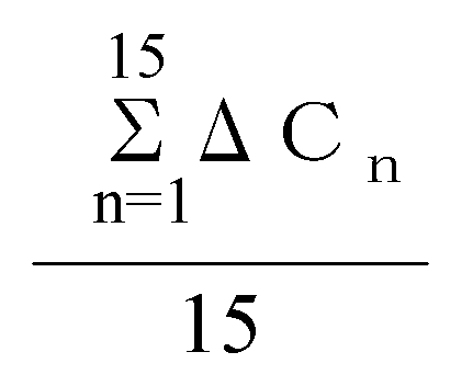
(1)
さらに、当該15種類の修正マンセル色票の飽和度差の最大値をΔCmax、飽和度差の最小値をΔCminとした場合に、最大飽和度差と最小飽和度差の間の差(最大最小飽和度差間差)である
(ΔCmax-ΔCmin)
も重要な指標と考えた。これは試験光と実験用基準光あるいは実験用擬似基準光を用いて視覚実験を行うに当たり、さまざまな物体、あるいは物体の色の見えを全体として評価し、自然で、生き生きとした、視認性の高い、快適な、色の見え、物体の見えを実現する手段として、本発明で特別に選択した当該15種類の修正マンセル色票の飽和度差に関わる種々の特性は重要な指標になると考えたからである。
ΔCn=√{(a* nSSL)2+(b* nSSL)2}-√{(a* nref)2+(b* nref)2}
と定義した。また、当該15種類の修正マンセル色票の飽和度差の平均値である下記式(1)も重要な指標と考えた。
さらに、当該15種類の修正マンセル色票の飽和度差の最大値をΔCmax、飽和度差の最小値をΔCminとした場合に、最大飽和度差と最小飽和度差の間の差(最大最小飽和度差間差)である
(ΔCmax-ΔCmin)
も重要な指標と考えた。これは試験光と実験用基準光あるいは実験用擬似基準光を用いて視覚実験を行うに当たり、さまざまな物体、あるいは物体の色の見えを全体として評価し、自然で、生き生きとした、視認性の高い、快適な、色の見え、物体の見えを実現する手段として、本発明で特別に選択した当該15種類の修正マンセル色票の飽和度差に関わる種々の特性は重要な指標になると考えたからである。
[分光分布に関する定量指標の導入]
本発明では、分光分布の放射計測学的特性、測光学的特性も議論するために、以下の2つの定量指標を導入した。ひとつは指標Acgであって、もうひとつの指標は放射効率K(lm/W)である。
本発明では、分光分布の放射計測学的特性、測光学的特性も議論するために、以下の2つの定量指標を導入した。ひとつは指標Acgであって、もうひとつの指標は放射効率K(lm/W)である。
指標Acgは、実験用基準光もしくは実験用擬似基準光による色の見えと、試験光による色の見えの差を、分光分布あるいはスペクトル形状が有する放射計測学的特性と測光学的特性としても記述することを試みたものである。種々の検討の結果、指標Acgを本発明では以下のように定義した。
照明対象物の位置で測定した場合における(本発明の照明方法に係る)、又は、発光装置からの主たる放射方向に出射される光を測定した場合における(本発明の発光装置に係る)、異なる色刺激となる計算用基準光と試験光の分光分布をそれぞれφref(λ)、 φSSL(λ)とし、等色関数をx(λ)、y(λ)、z(λ)、計算用基準光と試験光に対応する三刺激値をそれぞれ(Xref、Yref、Zref)、(XSSL、YSSL、ZSSL)とする。ここで、計算用基準光と試験光に関して、kを定数として、以下が成立する。
Yref=k∫φref(λ)・y(λ)dλ
YSSL=k∫φSSL(λ)・y(λ)dλ
ここで、計算用基準光と試験光の分光分布をそれぞれのYで規格化した規格化分光分布を
Sref(λ)=φref(λ)/Yref
SSSL(λ)=φSSL(λ)/YSSL
と定義し、これら規格化基準光分光分布と規格化試験光分光分布の差を
ΔS(λ)=Sref(λ)-SSSL(λ)
とした。さらに、ここで、指標Acgを以下のように定義した。

なお、ここで各積分の上下限波長は、それぞれ
Λ1=380nm
Λ2=495nm
Λ3=590nm
とした。
Yref=k∫φref(λ)・y(λ)dλ
YSSL=k∫φSSL(λ)・y(λ)dλ
ここで、計算用基準光と試験光の分光分布をそれぞれのYで規格化した規格化分光分布を
Sref(λ)=φref(λ)/Yref
SSSL(λ)=φSSL(λ)/YSSL
と定義し、これら規格化基準光分光分布と規格化試験光分光分布の差を
ΔS(λ)=Sref(λ)-SSSL(λ)
とした。さらに、ここで、指標Acgを以下のように定義した。
なお、ここで各積分の上下限波長は、それぞれ
Λ1=380nm
Λ2=495nm
Λ3=590nm
とした。
また、Λ4は、以下の2つの場合に分けて定義をした。まず、規格化試験光分光分SSSL(λ)において、380nmから780nm内で、最長波長極大値を与える波長をλR(nm)、その分光強度をSSSL(λR)とした際に、λRよりも長波長側にあり、強度がSSSL(λR)/2となる波長をΛ4とした。もし、そのような波長が780nmまでの範囲内に存在しない場合は、Λ4は780nmとした。
指標Acgは色刺激となる放射に関わる可視域を大きく短波長領域(あるいは紫等も含む青領域)、中間波長領域(黄色等も含む緑色領域)、長波長領域(橙色等も含む赤領域)に分割し、数学的な規格化基準光分光分布に比較して、規格化試験光分光分布内の適切な位置に、適切な強度で、スペクトルの凹凸が存在するかどうかを判断する指標である。図33、図34に例示するように、長波長積分範囲は、最長波長極大値の位置によって異なる。また、試験光のCCTによって計算用基準光の選択は異なる。図33の場合は図中実線で示された試験光のCCTが5000K以上なので、基準の光は図中点線で示されるようにCIE昼光(CIE daylight)が選択されている。図34の場合は図中実線で示された試験光のCCTが5000K未満なので、基準の光は図中点線で示されるように黒体放射の光が選択されている。なお、図中網掛け部分は短波長領域、中間波長領域、長波長領域の積分範囲を模式的に示したものである。
短波長領域においては、数学的な規格化基準光分光分布よりも規格化試験光分光分布のスペクトル強度が強い場合に、指標Acgの第一項(ΔS(λ)の積分)はマイナスの値をとりやすい。中間波長領域においては、逆に、規格化基準光分光分布よりも規格化試験光分光分布のスペクトル強度が弱い場合に、指標Acgの第二項(-ΔS(λ)の積分)はマイナスの値をとりやすい。さらに、長波長領域においては、規格化基準光分光分布よりも規格化試験光分光分布のスペクトル強度が強い場合に、指標Acgの第三項(ΔS(λ)の積分)はマイナスの値をとりやすい指標となっている。
また、前記のように、計算用基準光は試験光のCCTによって変えられる。すなわち、計算用基準光は試験光のCCTが5000K未満の際には黒体放射の光が用いられ、試験光のCCTが5000K以上の際には定義されているCIE昼光(CIE daylight)が用いられる。指標Acgの値の導出においては、φref(λ)は、数学的に定義されている黒体放射の光かCIE昼光を用い、一方、φSSL(λ)はシミュレーションに用いた関数、あるいは実験で実測した値を用いた。
さらに、照明対象物の位置で測定した場合における(本発明の照明方法に係る)、又は、発光装置から出射された主たる放射方向の光を測定した場合における(本発明の発光装置に係る)試験光分光分布φSSL(λ)を評価するに当たり、放射効率 K (Luminous Efficacy of radiation)(lm/W)は、広く使用されている以下の定義を踏襲した。
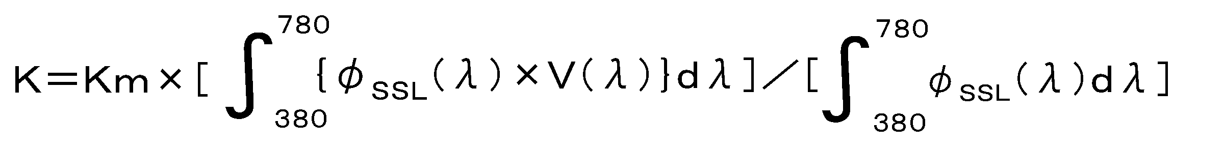
上記式において、
Km:最大視感度(lm/W)
V(λ):分光視感効率
λ:波長(nm)
である。
上記式において、
Km:最大視感度(lm/W)
V(λ):分光視感効率
λ:波長(nm)
である。
照明対象物の位置で測定した場合における(本発明の照明方法に係る)、又は、発光装置から出射された主たる放射方向の光を測定した場合における(本発明の発光装置に係る)試験光分光分布φSSL(λ)の放射効率K(lm/W)は、分光分布がその形状として有する効率であって、発光装置を構成するすべての材料特性に関する効率(例えば半導体発光素子の内部量子効率、光取り出し効率、蛍光体の内部量子効率、外部量子効率、封止剤の透光特性等々の効率)が100%であった際に、光源効率η(lm/W)となる量である。
[第二ステップ詳細]
前述の通り、第二ステップとしては、数学的に検討したスペクトル(試験光)を元に、パッケージLED光源、照明器具を試作した。また、計算用基準光に近接した色の見えとなる高Raかつ高Riである光(実験用擬似基準光)用の光源、これを内在した照明器具も試作した。
具体的には、青色半導体発光素子で緑色蛍光体、赤色蛍光体を励起した光源、青色半導体発光素子で黄色蛍光体、赤色蛍光体を励起した光源、紫色半導体発光素子で青色蛍光体、緑色蛍光体、赤色蛍光体を励起した光源を試作し、器具化した。
青色蛍光体としてはBAMまたはSBCAを用いた。緑色蛍光体としては、BSS、β-SiAlON、またはBSONを用いた。黄色蛍光体としてはYAGを用いた。赤色蛍光体としてはCASONまたはSCASNを用いた。
パッケージLEDを試作する際には、通常行われている方法を用いた。具体的には、電気的に導通可能な金属配線を内在させたセラミックパッケージ上に半導体発光素子(チップ)をフリップチップマウントした。次に、用いる蛍光体とバインダー樹脂を混合したスラリーを、蛍光体層として配置した。
パッケージLEDを準備した後には、これらを用いてMR16 Gu10、MR16 Gu5.3のLEDバルブなどに仕上げた。このLEDバルブ中には駆動用回路を内蔵させ、また、反射ミラー、レンズ等も搭載し、1種の照明器具に仕上げた。また、市販のLEDバルブも一部準備した。かつ、実験用基準光とすべくタングステンフィラメントを内在する白熱電球も準備した。
さらに、これらLEDバルブを多数配置し、比較視覚実験を行うための照明システムを製作した。ここでは、3種類のバルブを瞬時に切り替えて照明できるシステムをくみ上げた。駆動用電源線の一種は、タングステンフィラメントを有する白熱電球(実験用基準光)専用とし、その後段には可変トランスを配置し、100Vの入力電圧に対して、駆動電圧を110Vから130Vまで昇圧させることで、CCTを変化させられるようにした。また、駆動用電源線の残り2系統はLEDバルブ用とし、この中の1系統は実験用擬似基準光(LED光源)用、残り1系統は試験光用とした。
[第三ステップ詳細]
第三ステップとしては、実験用基準光(あるいは実験用擬似基準光)と試験光を切り替えて、多数の観察対象物の色の見えを被験者に評価してもらう比較視覚実験を行った。当該照明システムは暗室中に設置し外乱を排除した。また、観察対象物の位置における照度は、照明システムに搭載した実験用基準光(あるいは実験用擬似基準光)、試験光の器具数を変化させて、ほぼ一致させた。照度は約150lxから約5000lxの範囲で実験を行った。
実際に照明対象物、観察物としたものを以下に例示する。ここでは、紫色、青紫色、青色、青緑色、緑色、黄緑色、黄色、黄赤色、赤色、赤紫色等の全色相に渡る有彩色対象物を準備するように配慮した。さらに、白色物、黒色物などの無彩色の対象物も準備した。色を有する照明対象物を準備した。また、静物、生花、食品、衣料品、印刷物等、多数多種類なものを準備した。また、実験においては被験者(日本人)自身の肌も観察対象とした。なお、以下の物体名称前に一部付記した色名称は、通常の環境下でそのように見えるという意味で、厳密な色の表現ではない。
白色セラミック皿、ホワイトアスパラ、ホワイトマッシュルーム、白ガーベラ、白色ハンカチ、白Yシャツ、米飯、塩ゴマ、塩せんべい
紫色生花
青紫布製ハンカチ、ブルージーンズ、青緑タオル
緑色パプリカ、レタス、千切りキャベツ、ブロッコリー、緑ライム、緑色りんご
黄色バナナ、黄色パプリカ、黄緑色レモン、黄色ガーベラ、卵焼き
橙色オレンジ、橙色パプリカ、にんじん
赤色トマト、赤色りんご、赤色パプリカ、赤色ウインナー、梅干
ピンク色ネクタイ、ピンクガーベラ、しゃけ塩焼き
小豆色ネクタイ、ベージュ作業着、コロッケ、とんかつ、ごぼう、クッキー、チョコレート、
落花生、木製器
被験者(日本人)自身の肌
新聞紙、白背景上の黒文字を含むカラー印刷物(多色ずり)、文庫本、週刊誌
外壁材色見本(三菱樹脂社製 アルポリック 白、青、緑、黄色、赤)
カラーチェッカー(X―rite社製 Color checker classic 18色の有彩色と6種類の無彩色(白1、灰色4、黒1)を含む計24色の色票)
なお、カラーチェッカー中の各色票の名称とマンセル表記は、以下の通りである。
Name Munsell Notation
Dark skin 3.05 YR 3.69/3.20
Light skin 2.2 YR 6.47/4.10
Blue sky 4.3 PB 4.95/5.55
Foliage 6.65 GY 4.19/4.15
Blue flower 9.65 PB 5.47/6.70
Bluish green 2.5 BG 7/6
Orange 5 YR 6/11
Purplish blue 7.5 PB 4/10.7
Moderate red 2.5 R 5/10
Purple 5 P 3/7
Yellow green 5 GY 7.08/9.1
Orange yellow 10 YR 7/10.5
Blue 7.5 PB 2.90/12.75
Green 0.1 G 5.38/9.65
Red 5 R 4/12
Yellow 5 Y 8/11.1
Magenta 2.5 RP 5/12
Cyan 5 B 5/8
White N 9.5/
Neutral 8 N 8/
Neutral 6.5 N 6.5/
Neutral 5 N 5/
Neutral 3.5 N 3.5/
Black N 2/
なお、比較視覚実験で用いた各種照明対象物の色の見えと、計算で使用した15種類のマンセル色票の色の見えに関わる各種数学的指標との間に、相関があることは必ずしも自明ではない。これは視覚実験を通じて明らかとすることである。
視覚実験は、以下のような手順で行った。
準備した実験用基準光、実験用擬似基準光、試験光を、照明対象物の位置で測定したCCT毎に(本発明の照明方法に係る)、又は、準備した実験用基準光、実験用擬似基準光、試験光の、主たる放射方向に出射された光を計測し、それぞれをCCT毎に(本発明の発光装置に係る)、6実験用に分類をした。すなわち、以下の通りである。
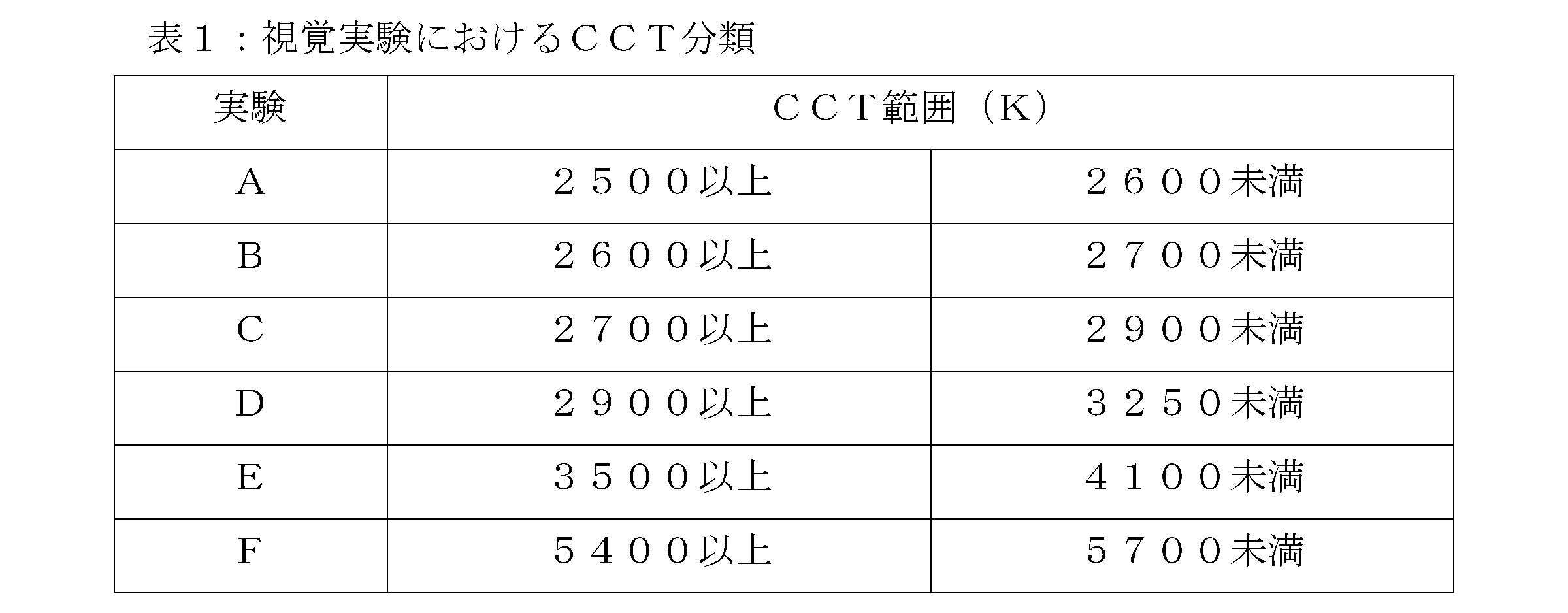
準備した実験用基準光、実験用擬似基準光、試験光を、照明対象物の位置で測定したCCT毎に(本発明の照明方法に係る)、又は、準備した実験用基準光、実験用擬似基準光、試験光の、主たる放射方向に出射された光を計測し、それぞれをCCT毎に(本発明の発光装置に係る)、6実験用に分類をした。すなわち、以下の通りである。
1つの視覚実験では、同一対象物を、実験用基準光(あるいは実験用擬似基準光)と試験光とを切り替えて照明し、いずれの光が屋外で見たような、自然で、生き生きとした、視認性の高い、快適な、色の見え、物体の見えを実現できるかを、被験者に相対的に判断してもらった。この際に優劣の判断理由も尋ねた。
[第四ステップ詳細 実験結果]
第四ステップでは、第二ステップで試作したLED光源/器具/システムを用いて、第三ステップで行った比較視覚実験の結果をまとめた。表2は実験Aに対応し、表3は実験Bに対応する結果である。以下同様に、表7は実験Fに対応する結果である。表2~7において、基準光に対する試験光の総合評価は、同程度の見えを表す「0」を中心に、試験光が若干好ましいとの評価は「1」、試験光が好ましいとの評価は「2」、試験光がより好ましいとの評価は「3」、試験光が非常に好ましいとの評価は「4」、試験光が格段に好ましいとの評価は「5」とした。一方、試験光が若干好ましくないとの評価を「-1」、試験光が好ましくないとの評価を「-2」、試験光がより好ましくないとの評価を「-3」、試験光が非常に好ましくないとの評価を「-4」、試験光が格段に好ましくないとの評価を「-5」とした。
第四ステップでは、第二ステップで試作したLED光源/器具/システムを用いて、第三ステップで行った比較視覚実験の結果をまとめた。表2は実験Aに対応し、表3は実験Bに対応する結果である。以下同様に、表7は実験Fに対応する結果である。表2~7において、基準光に対する試験光の総合評価は、同程度の見えを表す「0」を中心に、試験光が若干好ましいとの評価は「1」、試験光が好ましいとの評価は「2」、試験光がより好ましいとの評価は「3」、試験光が非常に好ましいとの評価は「4」、試験光が格段に好ましいとの評価は「5」とした。一方、試験光が若干好ましくないとの評価を「-1」、試験光が好ましくないとの評価を「-2」、試験光がより好ましくないとの評価を「-3」、試験光が非常に好ましくないとの評価を「-4」、試験光が格段に好ましくないとの評価を「-5」とした。
第四ステップでは、特に、視覚実験において、実験用基準光あるいは実験用擬似基準光で照明した場合よりも、試験光で照明した場合の照明対象物の色の見えが良好であったと判断された場合について、試験光に共通する分光分布の放射計測学的特性、測光学的特性を実測スペクトルから抽出することを試みた。すなわち、Acg、放射効率K(lm/W)、CCT(K)、Duvなどの数値に関して、照明対象物の位置(本発明の照明方法に係る)と、発光装置から主たる放射方向に出射された光(本発明の発光装置に係る)との特徴を抽出した。同時に、計算用基準光で照明した場合を仮定した当該15色票の色の見えと、照明対象物の位置で実測した試験光分光分布(本発明の照明方法に係る)、又は、発光装置から主たる放射方向に出射された光を実測した試験光分光分布(本発明の発光装置に係る)で 照明した場合を仮定した当該15色票の色の見えの間の差に関しても、|Δhn|、

、
ΔCn、(ΔCmax-ΔCmin)を指標としてまとめた。なお、|Δhn|、ΔCnは、nを選択すると値が変化するが、ここでは最大値と最小値を示した。これらの値も表2から表7に合わせて記載した。なお、照明対象物の色の見えに関して、被験者の総合的評価結果が照明対象物の位置における試験光(本発明の照明方法に係る)、又は、発光装置から出射された主たる放射方向の試験光(本発明の発光装置に係る)のDuv値に比較的依存していたので、表2から表7は、Duvの値が低下する順に並べた。
全体としては、本実験によって、Duvが適切な値で負の値をとり、かつ、|Δhn|、

、
ΔCn、(ΔCmax-ΔCmin)等が適切な範囲にある場合、又は、指標Acg等が適切な範囲にある場合に、試験光で照明していた実観察物の物体の見え、色の見えは、実験用基準光で照明した場合よりも好ましいと判断された。これはステップ1で「現在広く信じられている常識に照らした結果」に対して予想外であった。
ΔCn、(ΔCmax-ΔCmin)を指標としてまとめた。なお、|Δhn|、ΔCnは、nを選択すると値が変化するが、ここでは最大値と最小値を示した。これらの値も表2から表7に合わせて記載した。なお、照明対象物の色の見えに関して、被験者の総合的評価結果が照明対象物の位置における試験光(本発明の照明方法に係る)、又は、発光装置から出射された主たる放射方向の試験光(本発明の発光装置に係る)のDuv値に比較的依存していたので、表2から表7は、Duvの値が低下する順に並べた。
全体としては、本実験によって、Duvが適切な値で負の値をとり、かつ、|Δhn|、
ΔCn、(ΔCmax-ΔCmin)等が適切な範囲にある場合、又は、指標Acg等が適切な範囲にある場合に、試験光で照明していた実観察物の物体の見え、色の見えは、実験用基準光で照明した場合よりも好ましいと判断された。これはステップ1で「現在広く信じられている常識に照らした結果」に対して予想外であった。


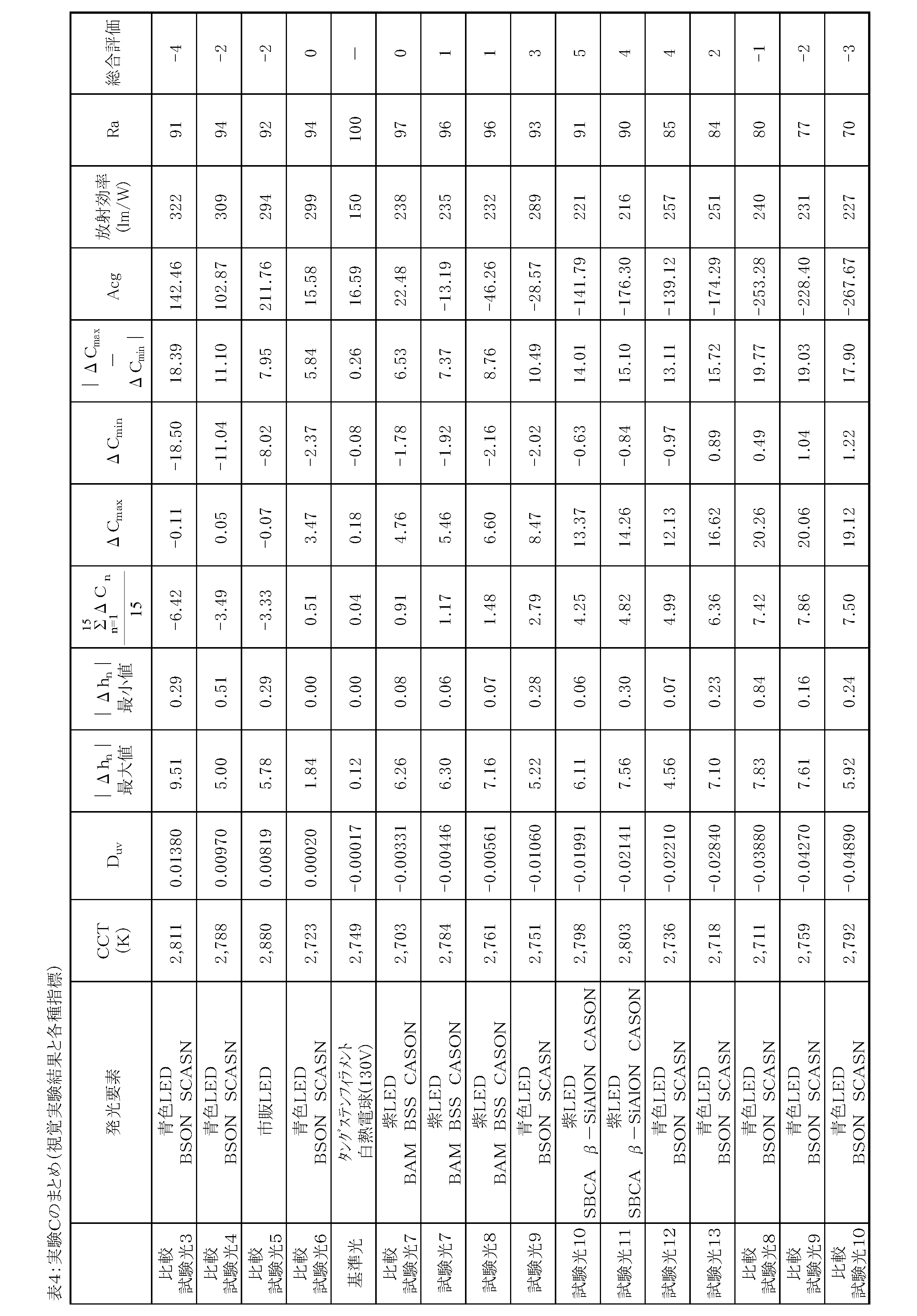


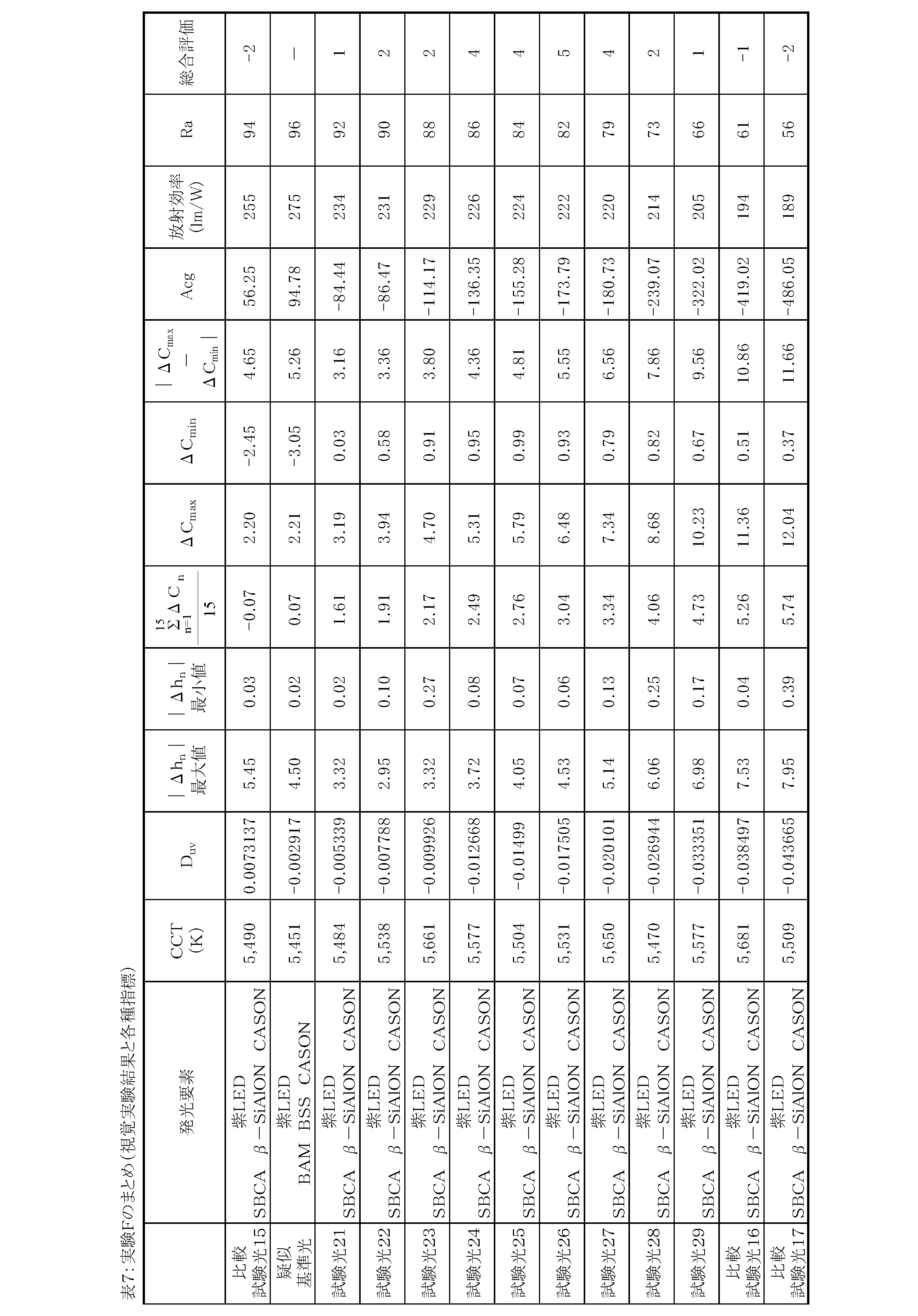
[第四ステップ詳細 考察]
以下実験結果を考察する。なお、表中の試験光及び比較試験光を総称して「試験光」と称する場合がある。
1)試験光のDuvが、実験用基準光(あるいは実験用疑似基準光)よりも正側であった場合
表4、表5、表7には、試験光のDuvが、実験用基準光(あるいは実験用疑似基準光)よりも正側の結果が含まれている。ここから、試験光のDuvが正になればなるほど、照明対象物の色の見えや物体の見えに関し、被験者は好ましくなくなったとの判断をしたことが分かる。具体的には、以下の通りであった。
以下実験結果を考察する。なお、表中の試験光及び比較試験光を総称して「試験光」と称する場合がある。
1)試験光のDuvが、実験用基準光(あるいは実験用疑似基準光)よりも正側であった場合
表4、表5、表7には、試験光のDuvが、実験用基準光(あるいは実験用疑似基準光)よりも正側の結果が含まれている。ここから、試験光のDuvが正になればなるほど、照明対象物の色の見えや物体の見えに関し、被験者は好ましくなくなったとの判断をしたことが分かる。具体的には、以下の通りであった。
照明された白色物の見えは、Duvが正になればなるほどより黄色み(緑色み)かかって見え、違和感がより増大したと被験者は判断した。照明されたカラーチェッカーの灰色部分の見えは、明度差がより視認しにくくなったと被験者は判断した。さらに、照明された印刷物の文字もより見にくくなったと被験者は指摘した。さらに、照明された各種有彩色の色の見えは、実験用基準光(あるいは実験用疑似基準光)で照明した場合と比較して、試験光のDuvが正になればなるほど、より不自然で、くすんで見えたと被験者は判断した。照明された各種外壁材色見本は屋外で見た色の見えと非常に異なって知覚され、自身の肌色も、不自然に、不健康に見えたと被験者は指摘した。また、同種類似色の生花花弁の色差は、実験用基準光で照明した場合と比較して、識別しにくく、輪郭が見にくくなったと被験者は指摘した。
また、これらの結果は、表4、表5、表7に記載した試験光のCCTにはあまり依存せず、また、発光装置の発光要素(発光材料)の構成にもあまり依存しないこともわかった。
試験光のDuvが正になればなるほど、全体的傾向としてRaが低下することから、これらの結果のいくつかは、ステップ1の数学的な詳細検討から予想可能な範囲であったと言える。
試験光のDuvが正になればなるほど、全体的傾向としてRaが低下することから、これらの結果のいくつかは、ステップ1の数学的な詳細検討から予想可能な範囲であったと言える。
2)試験光のDuvが、実験用基準光(あるいは実験用疑似基準光)よりも負側であった場合
表2から表7のすべてに、試験光のDuvが、実験用基準光(あるいは実験用疑似基準光)よりも負側の結果が含まれている。これらによれば、試験光のDuvが適正範囲で負であって、かつ、表中の各種指標が適正範囲に入っていれば、照明対象物の色の見えや物体の見えに関し、被験者は若干好ましい、好ましい、より好ましい、非常に好ましい、また、格段に好ましいと判断したことが分かる。一方、試験光のDuvが同様の範囲で負であっても、表中の各種指標が適正範囲になかった場合においては、表5に示されるように、試験光による色の見えや物体の見えが好ましくないと判断されたことも分かる。
表2から表7のすべてに、試験光のDuvが、実験用基準光(あるいは実験用疑似基準光)よりも負側の結果が含まれている。これらによれば、試験光のDuvが適正範囲で負であって、かつ、表中の各種指標が適正範囲に入っていれば、照明対象物の色の見えや物体の見えに関し、被験者は若干好ましい、好ましい、より好ましい、非常に好ましい、また、格段に好ましいと判断したことが分かる。一方、試験光のDuvが同様の範囲で負であっても、表中の各種指標が適正範囲になかった場合においては、表5に示されるように、試験光による色の見えや物体の見えが好ましくないと判断されたことも分かる。
ここで、試験光のDuvが適正範囲で負であって、かつ、表中の各種指標が適正範囲内の場合において、試験光で照明した場合の対象物の色の見えが、実験用基準光(あるいは実験用疑似基準光)で照明した場合のそれに比較して、自然で好ましい色の見え、好ましい物体の見えとなることは全く予想外であった。被験者が指摘した特長の詳細は以下の通りであった。
白色物は、試験光のDuvが適正範囲で負で、かつ、表中の各種指標が適正範囲内の場合では、実験用基準光(あるいは実験用疑似基準光)で照明した場合と比較して、黄色み(緑色み)が低減し、若干白く見えた、白く見えた、より白く見えた、非常に白く見えた、また、格段に白く見えたと被験者は判断した。また、最適範囲に近接するにつれ、より自然でより良好な見えになっていったことを指摘した。これは全く予想外の結果であった。
さらに、カラーチェッカーの灰色部分は、試験光のDuvが適正範囲で負で、かつ、表中の各種指標が適正範囲内の場合では、実験用基準光(あるいは実験用疑似基準光)で照明した場合と比較して、それぞれの明度差が、若干増したように見えた、増したように見えた、より増したように見えた、非常に増したように見えた、格段に増したように見えたと被験者は判断した。また、被験者は、最適範囲に近接するにつれ、より自然でより視認性の高い見えになっていったことを指摘した。これは全く予想外の結果であった。
さらに、カラーチェッカーの灰色部分は、試験光のDuvが適正範囲で負で、かつ、表中の各種指標が適正範囲内の場合では、実験用基準光(あるいは実験用疑似基準光)で照明した場合と比較して、それぞれの明度差が、若干増したように見えた、増したように見えた、より増したように見えた、非常に増したように見えた、格段に増したように見えたと被験者は判断した。また、被験者は、最適範囲に近接するにつれ、より自然でより視認性の高い見えになっていったことを指摘した。これは全く予想外の結果であった。
さらに、それぞれの無彩色色票の輪郭も、試験光のDuvが適正範囲で負で、かつ、表中の各種指標が適正範囲内の場合では、実験用基準光(あるいは実験用疑似基準光)で照明した場合と比較して、若干はっきり見えた、はっきり見えた、よりはっきり見えた、非常にはっきり見えた、格段にはっきり見えたと被験者は判断した。また、被験者は、最適範囲に近接するにつれ、より自然でより視認性の高い見えになっていったことを指摘した。これは全く予想外の結果であった。
さらに、印刷物の文字は、試験光のDuvが適正範囲で負で、かつ、表中の各種指標が適正範囲内の場合では、実験用基準光(あるいは実験用疑似基準光)で照明した場合と比較して、若干見やすくなった、見やすくなった、より見やすくなった、非常に見やすくなった、格段に見やすくなったと被験者は判断した。また、被験者は、最適範囲に近接するにつれ、より自然でより視認性の高い文字の見えになっていったことを指摘した。これは全く予想外の結果であった。
さらに、印刷物の文字は、試験光のDuvが適正範囲で負で、かつ、表中の各種指標が適正範囲内の場合では、実験用基準光(あるいは実験用疑似基準光)で照明した場合と比較して、若干見やすくなった、見やすくなった、より見やすくなった、非常に見やすくなった、格段に見やすくなったと被験者は判断した。また、被験者は、最適範囲に近接するにつれ、より自然でより視認性の高い文字の見えになっていったことを指摘した。これは全く予想外の結果であった。
さらに、各種有彩色の照明対象物の色の見えは、試験光のDuvが適正範囲で負で、かつ、表中の各種指標が適正範囲内の場合では、実験用基準光(あるいは実験用疑似基準光)で照明した場合と比較して、若干ではあるが自然な鮮やかさであった、自然な鮮やかさであった、より自然な鮮やかさであった、非常に自然な鮮やかさであった、また、格段に自然な鮮やかさであったと被験者は判断した。また、被験者は、最適範囲に近接するにつれ、より自然で、好ましい色の見えになっていったことを指摘した。これは全く予想外の結果であった。
さらに、各種外壁材色見本の色の見えは、試験光のDuvが適正範囲で負で、かつ、表中の各種指標が適正範囲内の場合では、実験用基準光(あるいは実験用疑似基準光)で照明した場合と比較して、屋外で見た際の記憶と、若干近接していた、近接していた、より近接していた、非常に近接していた、また、格段に近接していたと被験者は判断した。また、被験者は、最適範囲に近接するにつれ、より自然で、屋外で見た際の記憶と近接した好ましい色の見えになっていったことを指摘した。これは全く予想外の結果であった。
さらに、各種外壁材色見本の色の見えは、試験光のDuvが適正範囲で負で、かつ、表中の各種指標が適正範囲内の場合では、実験用基準光(あるいは実験用疑似基準光)で照明した場合と比較して、屋外で見た際の記憶と、若干近接していた、近接していた、より近接していた、非常に近接していた、また、格段に近接していたと被験者は判断した。また、被験者は、最適範囲に近接するにつれ、より自然で、屋外で見た際の記憶と近接した好ましい色の見えになっていったことを指摘した。これは全く予想外の結果であった。
さらに、被験者自身(日本人)の肌の色の見えは、試験光のDuvが適正範囲で負で、かつ、表中の各種指標が適正範囲内の場合では、実験用基準光(あるいは実験用疑似基準光)で照明した場合と比較して、若干自然に見えた、自然に見えた、より自然に見えた、非常に自然に見えた、また、格段に自然に見えたと被験者は判断した。また、被験者は、最適範囲に近接するにつれ、より自然で、健康的な好ましい色の見えになっていったことを指摘している。これは全く予想外の結果であった。
さらに、同種類似色の生花花弁の色差は、試験光のDuvが適正範囲で負で、かつ、表中の各種指標が適正範囲内の場合では、実験用基準光(あるいは実験用疑似基準光)で照明した場合と比較して、若干識別しやすかった、識別しやすかった、より識別しやすかった、非常に識別しやすかった、また、格段に識別しやすかったと被験者は判断した。また、被験者は、Duvが実験した範囲内で適正上限よりも負になればなるほど、より識別しやすかったことを指摘した。これは全く予想外の結果であった。
さらに、同種類似色の生花花弁の色差は、試験光のDuvが適正範囲で負で、かつ、表中の各種指標が適正範囲内の場合では、実験用基準光(あるいは実験用疑似基準光)で照明した場合と比較して、若干識別しやすかった、識別しやすかった、より識別しやすかった、非常に識別しやすかった、また、格段に識別しやすかったと被験者は判断した。また、被験者は、Duvが実験した範囲内で適正上限よりも負になればなるほど、より識別しやすかったことを指摘した。これは全く予想外の結果であった。
さらに、各種照明対象物は、試験光のDuvが適正範囲で負で、かつ、表中の各種指標が適正範囲内の場合では、実験用基準光(あるいは実験用疑似基準光)で照明した場合と比較して、若干輪郭がはっきり見えた、輪郭がはっきり見えた、より輪郭がはっきり見えた、非常に輪郭がはっきり見えた、また、格段に輪郭がはっきり見えたと被験者は判断した。また、被験者は、Duvが実験した範囲内で適正上限よりも負になればなるほど、より輪郭がはっきり見えたことを指摘した。これは全く予想外の結果であった。
試験光のDuvが負になればなるほど、全体的傾向としてRaが低下することからも、これらの結果は、ステップ1の数学的な詳細検討からは、全く予想外であったと言える。表2から表7にある通り、Raの値のみに注目すれば、Raが95以上である試験光も多数あったにも関わらず、たとえば、総合的に「格段に良好」とされた試験光のRaは82から91程度であった。また、今回の比較視覚実験は、ANSI C78.377-2008に記載されているDuvの範囲を超えて行っている。よって上記の結果は、現在の常識的推奨色度範囲の外に、照明された物体の色の見えに関する知覚良好領域があることを新たに見出したものと言える。
また、本発明の第一の実施態様に係る照明方法において、このような知覚を得るためにはDuv以外にも、表2から表7に記載の各種指標、すなわち、|Δhn|、

、
ΔCn、(ΔCmax-ΔCmin)が適正範囲にある必要があった。また、指標Acg、放射効率K(lm/W)が適正範囲にあることが好ましいことが解った。
ΔCn、(ΔCmax-ΔCmin)が適正範囲にある必要があった。また、指標Acg、放射効率K(lm/W)が適正範囲にあることが好ましいことが解った。
特に、視覚実験で良好と判断された試験光の結果から、|Δhn|、

、
ΔCn、(ΔCmax-ΔCmin)の特性を考えると、以下の傾向であったことが分かる。すなわち、良好な色の見え、物体の見えとなる試験光は、計算用基準光で照明した場合を仮定した当該15色票の色の見えと、実測した試験光分光分布で照明した場合を仮定した当該15色票の色の見えに関して、以下の特性を有していた。
ΔCn、(ΔCmax-ΔCmin)の特性を考えると、以下の傾向であったことが分かる。すなわち、良好な色の見え、物体の見えとなる試験光は、計算用基準光で照明した場合を仮定した当該15色票の色の見えと、実測した試験光分光分布で照明した場合を仮定した当該15色票の色の見えに関して、以下の特性を有していた。
試験光による照明と計算用基準光による照明の当該15色票の色相角差(|Δhn|)は比較的少なく、かつ、試験光による照明の当該15色票の平均的飽和度

が、計算用基準光による照明のそれと比較して適正な範囲で上がっていた。かつ、当該平均値だけでなく、15色票の飽和度(ΔCn)を個別に見ても、試験光による照明の当該15色票の各ΔCnが、計算用基準光による照明のそれらと比較して、極端に低下しているものも極端に向上しているものもなく、すべてが適正範囲にあり、この結果として最大最小飽和度差間差(ΔCmax-ΔCmin)が適正な範囲で狭かった。さらに、簡略化すれば、当該15色票に対して基準光での照明を仮定した場合に比較して、試験光での照明を仮定した場合は、当該15色票すべての色相において、色相角差が少なく、かつ、適正な範囲で15色票の飽和度が比較的均等に向上している場合が理想的であると推察できる。
が、計算用基準光による照明のそれと比較して適正な範囲で上がっていた。かつ、当該平均値だけでなく、15色票の飽和度(ΔCn)を個別に見ても、試験光による照明の当該15色票の各ΔCnが、計算用基準光による照明のそれらと比較して、極端に低下しているものも極端に向上しているものもなく、すべてが適正範囲にあり、この結果として最大最小飽和度差間差(ΔCmax-ΔCmin)が適正な範囲で狭かった。さらに、簡略化すれば、当該15色票に対して基準光での照明を仮定した場合に比較して、試験光での照明を仮定した場合は、当該15色票すべての色相において、色相角差が少なく、かつ、適正な範囲で15色票の飽和度が比較的均等に向上している場合が理想的であると推察できる。
図35の実線は、表3にあって、総合判断として「格段に好ましい」と判断された試験光5の規格化試験光分光分布である。また、同図中点線は、当該試験光のCCTから算出された計算用基準光(黒体放射の光)の規格化分光分布である。一方、図36は、当該試験光5で照明した場合(実線)と、計算用基準光(黒体放射の光)で照明した場合(点線)を仮定した、当該15色票の色の見えに関するCIELABプロットである。なお、紙面垂直方向は明度であるが、ここでは簡便のためにa*、b*軸のみをプロットした。
さらに図37と図38は、表5の中で、総合判断として「格段に好ましい」と判断された試験光15の結果を上記と同様にまとめたもので、図39と図40は、表6中で、総合判断として「格段に好ましい」と判断された試験光19の結果を上記と同様にまとめたものである。
さらに図37と図38は、表5の中で、総合判断として「格段に好ましい」と判断された試験光15の結果を上記と同様にまとめたもので、図39と図40は、表6中で、総合判断として「格段に好ましい」と判断された試験光19の結果を上記と同様にまとめたものである。
この様に視覚実験で好ましい色の見え、物体の見えとなった場合は、当該15色票に対する基準光での照明を仮定した場合に比較して、試験光での照明を仮定した場合に、当該15色票すべての色相において、色相角差が少なく、かつ、適正な範囲で15色票の飽和度が比較的均等に向上していることが分かる。また、この観点で4000K近傍のCCTは、好ましいことも分かる。
一方、Duvが適正な範囲で負の値を有する場合であっても、たとえば表5中のDuv≒-0.01831である比較試験光14の場合には、視覚実験において試験光による見えが好ましくないと判断されている。これは、|Δhn|、

、
ΔCn、(ΔCmax-ΔCmin)の特性のうちいくつかが適正でなかったと考えられる。図41、図42は比較試験光14について、図35、図36等と同様に規格化分光分布と15色票の色の見えに関するCIELABプロットを行った結果である。この図からも明らかなように、当該15色票に対して基準光での照明を仮定した場合と、試験光での照明を仮定した場合とを比較すると、当該15色票のいくつかの色相において、色相角差がおおきく、また、15色票の飽和度が非常に不均等に変化していることが分かる。
ΔCn、(ΔCmax-ΔCmin)の特性のうちいくつかが適正でなかったと考えられる。図41、図42は比較試験光14について、図35、図36等と同様に規格化分光分布と15色票の色の見えに関するCIELABプロットを行った結果である。この図からも明らかなように、当該15色票に対して基準光での照明を仮定した場合と、試験光での照明を仮定した場合とを比較すると、当該15色票のいくつかの色相において、色相角差がおおきく、また、15色票の飽和度が非常に不均等に変化していることが分かる。
視覚実験結果と考察から、各定量指標は、以下の範囲が好ましいことが分かる。
本発明の第一の実施態様に係る照明方法におけるDuvは、-0.0040以下であって、若干好ましくは-0.0042以下であって、好ましくは、-0.0070以下であって、より好ましくは-0.0100以下であって、非常に好ましくは-0.0120以下であって、格段に好ましくは-0.0160以下であった。
また、本発明の第一の実施態様に係る照明方法におけるDuvは、-0.0350以上であって、若干好ましくは-0.0340以上であって、好ましくは、-0.0290以上であって、より好ましくは-0.0250以上であって、非常に好ましくは-0.0230以上であって、格段に好ましくは-0.0200以上であった。
本発明の第一の実施態様に係る照明方法におけるDuvは、-0.0040以下であって、若干好ましくは-0.0042以下であって、好ましくは、-0.0070以下であって、より好ましくは-0.0100以下であって、非常に好ましくは-0.0120以下であって、格段に好ましくは-0.0160以下であった。
また、本発明の第一の実施態様に係る照明方法におけるDuvは、-0.0350以上であって、若干好ましくは-0.0340以上であって、好ましくは、-0.0290以上であって、より好ましくは-0.0250以上であって、非常に好ましくは-0.0230以上であって、格段に好ましくは-0.0200以上であった。
本発明の第一の実施態様に係る照明方法における|Δhn|は9.0以下であって、非常に好ましくは8.4以下であって、格段に好ましくは7.3以下であった。また|Δhn|は、さらに小さいことがより好ましいと考えられ、6.0以下がより格段に好ましく、5.0以下が更に格段に好ましく、4.0以下が特に格段に好ましいと考えられる。
なお、本発明の第一の実施態様に係る照明方法における|Δhn|は0以上で、視覚実験時の最小値は0.0029であった。さらに、視覚実験で実試験光を用いた検討がなされ、当該検討中の好ましい実験結果の内側にある|Δhn|の好ましい範囲は、8.3以下、0.003以上であった。
なお、本発明の第一の実施態様に係る照明方法における|Δhn|は0以上で、視覚実験時の最小値は0.0029であった。さらに、視覚実験で実試験光を用いた検討がなされ、当該検討中の好ましい実験結果の内側にある|Δhn|の好ましい範囲は、8.3以下、0.003以上であった。
本発明の第一の実施態様に係る照明方法における

は、1.0以上であって、若干好ましくは1.1以上であって、好ましくは、1.9以上であって、非常に好ましくは2.3以上であって、格段に好ましくは2.6以上であった。
また、7.0以下であって、好ましくは6.4以下であって、非常に好ましくは、5.1以下であって、格段に好ましくは4.7以下であった。
なお、視覚実験で実試験光を用いた検討がなされ、当該検討中の好ましい実験結果の内側にある上記指標の好ましい範囲は、1.2以上、6.3以下であった。
は、1.0以上であって、若干好ましくは1.1以上であって、好ましくは、1.9以上であって、非常に好ましくは2.3以上であって、格段に好ましくは2.6以上であった。
また、7.0以下であって、好ましくは6.4以下であって、非常に好ましくは、5.1以下であって、格段に好ましくは4.7以下であった。
なお、視覚実験で実試験光を用いた検討がなされ、当該検討中の好ましい実験結果の内側にある上記指標の好ましい範囲は、1.2以上、6.3以下であった。
本発明の第一の実施態様に係る照明方法におけるΔCnは、-3.8以上であって、若干好ましくは-3.5以上であって、非常に好ましくは-2.5以上であって、格段に好ましくは-0.7以上であった。
また、本発明の第一の実施態様に係る照明方法におけるΔCnは、18.6以下であって、非常に好ましくは17.0以下であって、格段に好ましくは15.0以下であった。さらに、視覚実験で実試験光を用いた検討がなされ、当該検討中の好ましい実験結果の内側にあるΔCnの好ましい範囲は、-3.4以上、16.8以下であった。
また、本発明の第一の実施態様に係る照明方法におけるΔCnは、18.6以下であって、非常に好ましくは17.0以下であって、格段に好ましくは15.0以下であった。さらに、視覚実験で実試験光を用いた検討がなされ、当該検討中の好ましい実験結果の内側にあるΔCnの好ましい範囲は、-3.4以上、16.8以下であった。
本発明の第一の実施態様に係る照明方法における(ΔCmax-ΔCmin)は、19.6以下であるが、17.9以下であることが非常に好ましく、15.2以下であることが格段に好ましかった。加えて、(ΔCmax-ΔCmin)は小さいことがより好ましいと考えられ、14.0以下がさらに格段に好ましく、13.0以下が非常に格段に好ましいと考えられる。
また、本発明の第一の実施態様に係る照明方法における(ΔCmax-ΔCmin)は2.8以上で、視覚実験時の最小値は3.16であった。さらに、視覚実験で実試験光を用いた検討がなされ、当該検討中の好ましい実験結果の内側にある(ΔCmax-ΔCmin)の好ましい範囲は、3.2以上、17.8以下であった。
また、本発明の第一の実施態様に係る照明方法における(ΔCmax-ΔCmin)は2.8以上で、視覚実験時の最小値は3.16であった。さらに、視覚実験で実試験光を用いた検討がなされ、当該検討中の好ましい実験結果の内側にある(ΔCmax-ΔCmin)の好ましい範囲は、3.2以上、17.8以下であった。
一方、表2から表7を用いて、視覚実験で好ましい特性と総合的に判断された試験光に付随する特性を、試験光分光分布が有する放射計測学的特性と測光学的特性とで代表させることも試みた。
この場合もDuv値は、これまで考察してきたとおりであって、-0.0040以下であって、若干好ましくは-0.0042以下であって、好ましくは、-0.0070以下であって、より好ましくは-0.0100以下であって、非常に好ましくは-0.0120以下であって、格段に好ましくは-0.0160以下であった。
また、本発明におけるDuvは、-0.0350以上であって、若干好ましくは-0.0340以上であって、好ましくは、-0.0290以上であって、より好ましくは-0.0250以上であって、非常に好ましくは-0.0230以上であって、格段に好ましくは-0.0200以上であった。
また、本発明におけるDuvは、-0.0350以上であって、若干好ましくは-0.0340以上であって、好ましくは、-0.0290以上であって、より好ましくは-0.0250以上であって、非常に好ましくは-0.0230以上であって、格段に好ましくは-0.0200以上であった。
一方、指標Acgに関しては、以下の様であった。
表2から表7の結果より、本発明の第一の実施態様に係る照明方法の好適な分光分布はAcgが-10以下であって-360以上であった。正確な定義は前述の通りであるが、この物理的なおおよその意味、見通しの良い解釈は、以下の通りである。Acgが適切な範囲で負の値を取るとの意味は、規格化試験光分光分布に適切な凹凸があり、380nmから495nm間の短波長領域では、数学的な規格化基準光分光分布よりも規格化試験光分光分布の放射束強度が強い傾向にあり、および/または、495nmから590nmの中間波長領域では、数学的な規格化基準光分光分布よりも規格化試験光分光分布の放射束強度が弱い傾向にあり、および/または、590nmからΛ4までの長波長領域では、数学的な規格化基準光分光分布よりも規格化試験光分光分布の放射束強度が強い傾向にあることを意味している。Acgは短波長領域、中間波長領域、長波長領域におけるそれぞれの要素の総和なので、各個別の要素は、必ずしも上記傾向でない場合もあり得る。そのうえで、Acgが定量的に-10以下-360以上の場合に、良好な色の見え、良好な物体の見えとなったと理解できる。
表2から表7の結果より、本発明の第一の実施態様に係る照明方法の好適な分光分布はAcgが-10以下であって-360以上であった。正確な定義は前述の通りであるが、この物理的なおおよその意味、見通しの良い解釈は、以下の通りである。Acgが適切な範囲で負の値を取るとの意味は、規格化試験光分光分布に適切な凹凸があり、380nmから495nm間の短波長領域では、数学的な規格化基準光分光分布よりも規格化試験光分光分布の放射束強度が強い傾向にあり、および/または、495nmから590nmの中間波長領域では、数学的な規格化基準光分光分布よりも規格化試験光分光分布の放射束強度が弱い傾向にあり、および/または、590nmからΛ4までの長波長領域では、数学的な規格化基準光分光分布よりも規格化試験光分光分布の放射束強度が強い傾向にあることを意味している。Acgは短波長領域、中間波長領域、長波長領域におけるそれぞれの要素の総和なので、各個別の要素は、必ずしも上記傾向でない場合もあり得る。そのうえで、Acgが定量的に-10以下-360以上の場合に、良好な色の見え、良好な物体の見えとなったと理解できる。
本発明の第一の実施態様に係る照明方法におけるAcgは、好適には-10以下であって、若干好ましくは-11以下であって、より好ましくは-28以下であって、非常に好ましくは-41以下であって、格段に好ましくは-114以下であった。
また、本発明の第一の実施態様に係る照明方法においては、Acgは好適には-360以上であって、若干好ましくは-330以上であって、好ましくは-260以上であって、非常に好ましくは-181以上であって、格段に好ましくは-178以上であった。
なお、視覚実験で実試験光を用いた検討がなされ、当該検討中の好ましい実験結果の内側にあるAcgの好ましい範囲は、-322以上、-12以下であった。
また、本発明の第一の実施態様に係る照明方法においては、Acgは好適には-360以上であって、若干好ましくは-330以上であって、好ましくは-260以上であって、非常に好ましくは-181以上であって、格段に好ましくは-178以上であった。
なお、視覚実験で実試験光を用いた検討がなされ、当該検討中の好ましい実験結果の内側にあるAcgの好ましい範囲は、-322以上、-12以下であった。
さらに、本発明第一の実施態様に係るは色の見えが良く効率も高い試験光の実現を目指したが、放射効率Kに関しては、以下の通りであった。
本発明の第一の実施態様に係る照明方法による分光分布が有する放射効率は、好適には180(lm/W)から320(lm/W)の範囲であって、通常の白熱電球等の値である150(lm/W)よりも最低でも20%以上高かった。これは半導体発光素子からの放射や蛍光体からの放射を内在しており、かつ、V(λ)との関係において、分光分布の適切な位置に適切な凹凸があったためであると考えられる。色の見えとの両立との観点では、本発明の照明方法の放射効率は、以下の範囲が好ましかった。
本発明の第一の実施態様に係る照明方法による分光分布が有する放射効率は、好適には180(lm/W)から320(lm/W)の範囲であって、通常の白熱電球等の値である150(lm/W)よりも最低でも20%以上高かった。これは半導体発光素子からの放射や蛍光体からの放射を内在しており、かつ、V(λ)との関係において、分光分布の適切な位置に適切な凹凸があったためであると考えられる。色の見えとの両立との観点では、本発明の照明方法の放射効率は、以下の範囲が好ましかった。
本発明の第一の実施態様に係る照明方法による放射効率Kは、好適には180(lm/W)以上であったが、若干好ましくは205(lm/W)以上であって、好ましくは208(lm/W)以上であって、非常に好ましくは215(lm/W)以上であった。一方、放射効率Kは理想的には高い方が良いが、本発明においては、好適には320(lm/W)以下であって、色の見えとのバランスから、282(lm/W)以下が若干好ましく、232(lm/W)以下が好ましく、231(lm/W)以下が格段に好ましかった。
なお、視覚実験で実試験光を用いた検討がなされ、当該検討中の好ましい実験結果の内側にあるKの好ましい範囲は、206(lm/W)以上、288(lm/W)以下であった。
なお、視覚実験で実試験光を用いた検討がなされ、当該検討中の好ましい実験結果の内側にあるKの好ましい範囲は、206(lm/W)以上、288(lm/W)以下であった。
さらに本発明の第一の実施態様に係る照明方法におけるCCTに関しては、以下のようなことが分かった。比較視覚実験によって、好ましいと判断された各種指標すなわち|Δhn|、

、
ΔCn、(ΔCmax-ΔCmin)をより適切な値とするためには、本発明の照明方法において、CCTは4000Kに近い値をとることが好ましかった。これは4000K付近の光は基準の光を見てもその分光分布が波長にあまり依存せずに等エネルギー的であって、基準の光に対して容易に凹凸を形成した試験光分光分布が実現できるためと考えられる。換言すると、他のCCTの場合と比較しても、|Δhn|と(ΔCmax-ΔCmin)を比較的小さく保持したまま、

を増加させ、大多数の色票に対するΔCnを所望の値に容易に制御可能である。
ΔCn、(ΔCmax-ΔCmin)をより適切な値とするためには、本発明の照明方法において、CCTは4000Kに近い値をとることが好ましかった。これは4000K付近の光は基準の光を見てもその分光分布が波長にあまり依存せずに等エネルギー的であって、基準の光に対して容易に凹凸を形成した試験光分光分布が実現できるためと考えられる。換言すると、他のCCTの場合と比較しても、|Δhn|と(ΔCmax-ΔCmin)を比較的小さく保持したまま、
を増加させ、大多数の色票に対するΔCnを所望の値に容易に制御可能である。
よって、本発明の第一の実施態様に係る照明方法におけるCCTは1800Kから15000Kであることが若干好ましく、2000Kから10000Kであることが好ましく、2300Kから7000Kであることがより好ましく、2600Kから6600Kであることが非常に好ましく、2900Kから5800Kであることが格段に好ましく、3400Kから5100Kであることが最も好ましい。
なお、視覚実験で実試験光を用いた検討がなされ、当該検討中の好ましい実験結果の内側にあるCCTの好ましい範囲は、2550(K)以上、5650(K)以下であった。
なお、視覚実験で実試験光を用いた検討がなされ、当該検討中の好ましい実験結果の内側にあるCCTの好ましい範囲は、2550(K)以上、5650(K)以下であった。
一方、本発明の第二の実施態様に係る発光装置において、このような知覚を得るためにはDuv以外にも、表2から表7に記載の指標Acgが適正範囲にある必要があった。また、各種指標、すなわち、放射効率K(lm/W)、|Δhn|、

、
ΔCn、(ΔCmax-ΔCmin)、が適正範囲にあることが好ましいことが解った。
ΔCn、(ΔCmax-ΔCmin)、が適正範囲にあることが好ましいことが解った。
第一に、視覚実験で良好と判断された試験光の結果から、Duvと、指標Acgに関しては、以下のようであった。
先ず、Duv値は、-0.0040以下であって、若干好ましくは-0.0042以下であって、好ましくは、-0.0070以下であって、より好ましくは-0.0100以下であって、非常に好ましくは-0.0120以下であって、格段に好ましくは-0.0160以下であった。
また、本発明におけるDuvは、-0.0350以上であって、若干好ましくは-0.0340以上であって、好ましくは、-0.0290以上であって、より好ましくは-0.0250以上であって、非常に好ましくは-0.0230以上であって、格段に好ましくは-0.0200以上であった。
また、本発明におけるDuvは、-0.0350以上であって、若干好ましくは-0.0340以上であって、好ましくは、-0.0290以上であって、より好ましくは-0.0250以上であって、非常に好ましくは-0.0230以上であって、格段に好ましくは-0.0200以上であった。
さらに、表2から表7の結果より、本発明の第二の実施態様に係る発光装置において分光分布はAcgが-10以下であって-360以上であった。正確な定義は前述の通りであるが、この物理的なおおよその意味、見通しの良い解釈は、以下の通りである。Acgが適切な範囲で負の値を取るとの意味は、規格化試験光分光分布に適切な凹凸があり、380nmから495nm間の短波長領域では、数学的な規格化基準光分光分布よりも規格化試験光分光分布の放射束強度が強い傾向にあり、および/または、495nmから590nmの中間波長領域では、数学的な規格化基準光分光分布よりも規格化試験光分光分布の放射束強度が弱い傾向にあり、および/または、590nmからΛ4までの長波長領域では、数学的な規格化基準光分光分布よりも規格化試験光分光分布の放射束強度が強い傾向にあることを意味している。そのうえで、Acgが定量的に-10以下-360以上の場合に、良好な色の見え、良好な物体の見えとなったと理解できる。
本発明の第二の実施態様に係る発光装置から主たる放射方向に出射される光の分光分布から導出されるAcgは、-10以下であって、若干好ましくは-11以下であって、より好ましくは-28以下であって、非常に好ましくは-41以下であって、格段に好ましくは-114以下であった。
また、本発明の第二の実施態様に係る発光装置から主たる放射方向に出射される光の分光分布から導出されるAcgは-360以上であって、若干好ましくは-330以上であって、好ましくは-260以上であって、非常に好ましくは-181以上であって、格段に好ましくは-178以上であった。
なお、視覚実験で実試験光を用いた検討がなされ、当該検討中の好ましい実験結果の内側にあるAcgの好ましい範囲は、-322以上、-12以下であった。
また、本発明の第二の実施態様に係る発光装置から主たる放射方向に出射される光の分光分布から導出されるAcgは-360以上であって、若干好ましくは-330以上であって、好ましくは-260以上であって、非常に好ましくは-181以上であって、格段に好ましくは-178以上であった。
なお、視覚実験で実試験光を用いた検討がなされ、当該検討中の好ましい実験結果の内側にあるAcgの好ましい範囲は、-322以上、-12以下であった。
第二に、本発明は色の見えが良く効率も高い試験光の実現を目指したが、放射効率Kに関しては、以下の通りであった。
本発明の第二の実施態様に係る発光装置による分光分布が有する放射効率は、好適には180(lm/W)から320(lm/W)の範囲であって、通常の白熱電球等の値である150(lm/W)よりも最低でも20%以上高かった。これは半導体発光素子からの放射や蛍光体からの放射を内在しており、かつ、V(λ)との関係において、分光分布の適切な位置に適切な凹凸があったためであると考えられる。色の見えとの両立との観点では、本発明の第二の実施態様に係る発光装置から主たる放射方向に出射される光が有する分光分布から求められる放射効率は、以下の範囲が好ましかった。
本発明の第二の実施態様に係る発光装置による分光分布が有する放射効率は、好適には180(lm/W)から320(lm/W)の範囲であって、通常の白熱電球等の値である150(lm/W)よりも最低でも20%以上高かった。これは半導体発光素子からの放射や蛍光体からの放射を内在しており、かつ、V(λ)との関係において、分光分布の適切な位置に適切な凹凸があったためであると考えられる。色の見えとの両立との観点では、本発明の第二の実施態様に係る発光装置から主たる放射方向に出射される光が有する分光分布から求められる放射効率は、以下の範囲が好ましかった。
本発明の第二の実施態様に係る発光装置による放射効率Kは、好適には180(lm/W)以上であったが、若干好ましくは205(lm/W)以上であって、好ましくは208(lm/W)以上であって、非常に好ましくは215(lm/W)以上であった。一方、放射効率Kは理想的には高い方が良いが、本発明においては、好適には320(lm/W)以下であって、色の見えとのバランスから、282(lm/W)以下が若干好ましく、232(lm/W)以下が好ましく、231(lm/W)以下が格段に好ましかった。
なお、視覚実験で実試験光を用いた検討がなされ、当該検討中の好ましい実験結果の内側にあるKの好ましい範囲は、206(lm/W)以上、288(lm/W)以下であった。
なお、視覚実験で実試験光を用いた検討がなされ、当該検討中の好ましい実験結果の内側にあるKの好ましい範囲は、206(lm/W)以上、288(lm/W)以下であった。
第三に、|Δhn|、

、
ΔCn、(ΔCmax-ΔCmin)の特性を考えると、以下の傾向であったことが分かる。すなわち、良好な色の見え、物体の見えとなる試験光は、計算用基準光で照明した場合を仮定した当該15色票の色の見えと、実測した試験光分光分布で照明した場合を仮定した当該15色票の色の見えに関して、以下の特性を有していた。
ΔCn、(ΔCmax-ΔCmin)の特性を考えると、以下の傾向であったことが分かる。すなわち、良好な色の見え、物体の見えとなる試験光は、計算用基準光で照明した場合を仮定した当該15色票の色の見えと、実測した試験光分光分布で照明した場合を仮定した当該15色票の色の見えに関して、以下の特性を有していた。
試験光による照明と計算用基準光による照明の当該15色票の色相角差(|Δhn|)は比較的少なく、かつ、試験光による照明の当該15色票の平均的飽和度

が、計算用基準光による照明のそれと比較して適正な範囲で上がっていた。かつ、当該平均値だけでなく、15色票の飽和度(ΔCn)を個別に見ても、試験光による照明の当該15色票の各ΔCnが、計算用基準光による照明のそれらと比較して、極端に低下しているものも極端に向上しているものもなく、すべてが適正範囲にあり、この結果として最大最小飽和度差間差(ΔCmax-ΔCmin)が適正な範囲で狭かった。さらに、簡略化すれば、当該15色票に対して基準光での照明を仮定した場合に比較して、試験光での照明を仮定した場合は、当該15色票すべての色相において、色相角差が少なく、かつ、適正な範囲で15色票の飽和度が比較的均等に向上している場合が理想的であると推察できる。
が、計算用基準光による照明のそれと比較して適正な範囲で上がっていた。かつ、当該平均値だけでなく、15色票の飽和度(ΔCn)を個別に見ても、試験光による照明の当該15色票の各ΔCnが、計算用基準光による照明のそれらと比較して、極端に低下しているものも極端に向上しているものもなく、すべてが適正範囲にあり、この結果として最大最小飽和度差間差(ΔCmax-ΔCmin)が適正な範囲で狭かった。さらに、簡略化すれば、当該15色票に対して基準光での照明を仮定した場合に比較して、試験光での照明を仮定した場合は、当該15色票すべての色相において、色相角差が少なく、かつ、適正な範囲で15色票の飽和度が比較的均等に向上している場合が理想的であると推察できる。
図35の実線は、表3にあって、総合判断として「格段に好ましい」と判断された試験光5の規格化試験光分光分布である。また、同図中点線は、当該試験光のCCTから算出された計算用基準光(黒体放射の光)の規格化分光分布である。一方、図36は、当該試験光5で照明した場合(実線)と、計算用基準光(黒体放射の光)で照明した場合(点線)を仮定した、当該15色票の色の見えに関するCIELABプロットである。なお、紙面垂直方向は明度であるが、ここでは簡便のためにa*、b*軸のみをプロットした。
さらに図37と図38は、表5の中で、総合判断として「格段に好ましい」と判断された試験光15の結果を上記と同様にまとめたもので、図39と図40は、表6中で、総合判断として「格段に好ましい」と判断された試験光19の結果を上記と同様にまとめたものである。
さらに図37と図38は、表5の中で、総合判断として「格段に好ましい」と判断された試験光15の結果を上記と同様にまとめたもので、図39と図40は、表6中で、総合判断として「格段に好ましい」と判断された試験光19の結果を上記と同様にまとめたものである。
この様に視覚実験で好ましい色の見え、物体の見えとなった場合は、当該15色票に対する基準光での照明を仮定した場合に比較して、試験光での照明を仮定した場合に、当該15色票すべての色相において、色相角差が少なく、かつ、適正な範囲で15色票の飽和度が比較的均等に向上していることが分かる。また、この観点で4000K近傍のCCTは、好ましいことも分かる。
一方、Duvが適正な範囲で負の値を有する場合であっても、たとえば表5中のDuv≒-0.01831である比較試験光14の場合には、視覚実験において試験光による見えが好ましくないと判断されている。これは、指標Acgの特性が適正でなかったと考えられる。図41、図42は比較試験光14について、図35、図36等と同様に規格化分光分布と15色票の色の見えに関するCIELABプロットを行った結果である。この図からも明らかなように、当該15色票に対して基準光での照明を仮定した場合と、試験光での照明を仮定した場合とを比較すると、当該15色票のいくつかの色相において、色相角差がおおきく、また、15色票の飽和度が非常に不均等に変化していることが分かる。
視覚実験結果と考察から、各定量指標は、以下の範囲が好ましいことが分かる。
本発明の第二の実施態様に係る発光装置におけるDuvは、前述の通り、-0.0040以下であって、若干好ましくは-0.0042以下であって、好ましくは、-0.0070以下であって、より好ましくは-0.0100以下であって、非常に好ましくは-0.0120以下であって、格段に好ましくは-0.0160以下であった。
また、本発明の第二の実施態様に係る発光装置におけるDuvは、-0.0350以上であって、若干好ましくは-0.0340以上であって、好ましくは、-0.0290以上であって、より好ましくは-0.0250以上であって、非常に好ましくは-0.0230以上であって、格段に好ましくは-0.0200以上であった。
本発明の第二の実施態様に係る発光装置における|Δhn|は9.0以下が好適であり、非常に好ましくは8.4以下であって、格段に好ましくは7.3以下であった。また|Δhn|は、さらに小さいことがより好ましいと考えられ、6.0以下がより格段に好ましく、5.0以下が更に格段に好ましく、4.0以下が特に格段に好ましいと考えられる。
なお、本発明の第二の実施態様に係る発光装置における|Δhn|は0以上が好適であり、視覚実験時の最小値は0.0029であった。さらに、視覚実験で実試験光を用いた検討がなされ、当該検討中の好ましい実験結果の内側にある|Δhn|の好ましい範囲は、8.3以下、0.003以上であった。
なお、本発明の第二の実施態様に係る発光装置における|Δhn|は0以上が好適であり、視覚実験時の最小値は0.0029であった。さらに、視覚実験で実試験光を用いた検討がなされ、当該検討中の好ましい実験結果の内側にある|Δhn|の好ましい範囲は、8.3以下、0.003以上であった。
本発明の第二の実施態様に係る発光装置における

は、1.0以上が好適であり、若干好ましくは1.1以上であって、好ましくは、1.9以上であって、非常に好ましくは2.3以上であって、格段に好ましくは2.6以上であった。
また、7.0以下であることが好適であり、好ましくは6.4以下であって、非常に好ましくは、5.1以下であって、格段に好ましくは4.7以下であった。
なお、視覚実験で実試験光を用いた検討がなされ、当該検討中の好ましい実験結果の内側にある上記指標の好ましい範囲は、1.2以上、6.3以下であった。
は、1.0以上が好適であり、若干好ましくは1.1以上であって、好ましくは、1.9以上であって、非常に好ましくは2.3以上であって、格段に好ましくは2.6以上であった。
また、7.0以下であることが好適であり、好ましくは6.4以下であって、非常に好ましくは、5.1以下であって、格段に好ましくは4.7以下であった。
なお、視覚実験で実試験光を用いた検討がなされ、当該検討中の好ましい実験結果の内側にある上記指標の好ましい範囲は、1.2以上、6.3以下であった。
本発明の第二の実施態様に係る発光装置におけるΔCnは、-3.8以上であることが好適であり、若干好ましくはは-3.5以上であって、非常に好ましくは-2.5以上であって、格段に好ましくは-0.7以上であった。
また、本発明の第二の実施態様に係る発光装置におけるΔCnは、18.6以下であることが好適であり、非常に好ましくは17.0以下であって、格段に好適には15.0以下であった。
なお、視覚実験で実試験光を用いた検討がなされ、当該検討中の好ましい実験結果の内側にあるΔCnの好ましい範囲は、-3.4以上、16.8以下であった。
また、本発明の第二の実施態様に係る発光装置におけるΔCnは、18.6以下であることが好適であり、非常に好ましくは17.0以下であって、格段に好適には15.0以下であった。
なお、視覚実験で実試験光を用いた検討がなされ、当該検討中の好ましい実験結果の内側にあるΔCnの好ましい範囲は、-3.4以上、16.8以下であった。
本発明の第二の実施態様に係る発光装置における(ΔCmax-ΔCmin)は、19.6以下であることが好適であり、17.9以下であることが非常に好ましく、15.2以下であることが格段に好ましかった。加えて、(ΔCmax-ΔCmin)は小さいことがより好ましいと考えられ、14.0以下がさらに格段に好ましく、13.0以下が非常に格段に好ましいと考えられる。
また、本発明の第二の実施態様に係る発光装置における(ΔCmax-ΔCmin)は2.8以上であることが好適であり、視覚実験時の最小値は3.16であった。さらに、視覚実験で実試験光を用いた検討がなされ、当該検討中の好ましい実験結果の内側にある(ΔCmax-ΔCmin)の好ましい範囲は、3.2以上、17.8以下であった。
また、本発明の第二の実施態様に係る発光装置における(ΔCmax-ΔCmin)は2.8以上であることが好適であり、視覚実験時の最小値は3.16であった。さらに、視覚実験で実試験光を用いた検討がなされ、当該検討中の好ましい実験結果の内側にある(ΔCmax-ΔCmin)の好ましい範囲は、3.2以上、17.8以下であった。
第四に、本発明の第二の実施態様に係る発光装置におけるCCTに関しては、以下のようなことが分かった。比較視覚実験によって、好ましいと判断された各種指標すなわち|Δhn|、

、
ΔCn、(ΔCmax-ΔCmin)をより適切な値とするためには、本発明の第二の実施態様に係る発光装置において、CCTは4000Kに近い値をとることが好ましかった。これは4000K付近の光は基準の光を見てもその分光分布が波長にあまり依存せずに等エネルギー的であって、基準の光に対して容易に凹凸を形成した試験光分光分布が実現できるためと考えられる。換言すると、他のCCTの場合と比較しても、|Δhn|と(ΔCmax-ΔCmin)を比較的小さく保持したまま、

を増加させ、大多数の色票に対するΔCnを所望の値に容易に制御可能である。
ΔCn、(ΔCmax-ΔCmin)をより適切な値とするためには、本発明の第二の実施態様に係る発光装置において、CCTは4000Kに近い値をとることが好ましかった。これは4000K付近の光は基準の光を見てもその分光分布が波長にあまり依存せずに等エネルギー的であって、基準の光に対して容易に凹凸を形成した試験光分光分布が実現できるためと考えられる。換言すると、他のCCTの場合と比較しても、|Δhn|と(ΔCmax-ΔCmin)を比較的小さく保持したまま、
を増加させ、大多数の色票に対するΔCnを所望の値に容易に制御可能である。
よって、本発明の第二の実施態様に係る発光装置におけるCCTは1800Kから15000Kであることが若干好ましく、2000Kから10000Kであることが好ましく、2300Kから7000Kであることがより好ましく、2600Kから6600Kであることが非常に好ましく、2900Kから5800Kであることが格段に好ましく、3400Kから5100Kであることが最も好ましい。
なお、視覚実験で実試験光を用いた検討がなされ、当該検討中の好ましい実験結果の内側にあるCCTの好ましい範囲は、2550(K)以上、5650(K)以下であった。
なお、視覚実験で実試験光を用いた検討がなされ、当該検討中の好ましい実験結果の内側にあるCCTの好ましい範囲は、2550(K)以上、5650(K)以下であった。
本発明の照明方法及び発光装置を実施するための好ましい実施形態を以下に説明するが、本発明の照明方法及び発光装置を実施するための態様は、以下の説明で用いたものに限定されない。
本発明の照明方法は、照明対象物に対して照射され、色刺激となる試験光の測光学的特性が適切な範囲にあり、かつ、計算用基準光で照明した場合を仮定した当該15色票の色の見えと、実測した試験光分光分布で照明した場合を仮定した当該15色票の色の見えの差が適切な範囲にあれば、発光装置の構成、材料等に制約はない。
本発明の発光装置は、発光装置から主たる放射方向に出射され、照明対象物に対して色刺激となる試験光の放射計測学的特性、測光学的特性が適切な範囲にあれば、発光装置の構成、材料等に制約はない。
本発明の照明方法又は発光装置を実施するための照明光源、当該照明光源を含む照明器具、当該照明光源や照明器具を含む照明システム等の発光装置は、少なくとも1つの発光要素である半導体発光素子を含んでいる。半導体発光素子を含む照明光源は、たとえば青色、緑色、赤色の種類の異なる複数の半導体発光素子を1つの照明光源中に内在していてもよく、また、1つの照明光源の中には青色半導体発光素子を含み、異なる1つの照明光源中に緑色半導体発光素子を含み、さらに異なる1つの照明光源中に赤色半導体発光素子を含み、これらが照明器具の中でレンズ、反射鏡、駆動回路等とともに一体とされて照明システムに提供されてもよい。さらに、1つの照明器具中に1つの照明光源があり、この中に単体の半導体発光素子が内在されているような場合であって、単体の照明光源、照明器具としては本発明の照明方法又は発光装置を実施できないものの、照明システム中に存在する異なる照明器具からの光との加法混色によって、照明システムとして放射される光が、照明対象物の位置で所望の特性を満足するようにしてもかまわないし、照明システムとして放射される光のうち主たる放射方向の光が、所望の特性を満足するようにしてもかまわない。いずれのような形態であっても、照明対象物に最終的に照射される色刺激としての光が、又は、発光装置から出射される光のうち主たる放射方向の光が、本発明の適切な条件を満たせばよい。
以下は、前記の適切な条件を満たしたうえで、本発明の第一の実施態様に係る照明方法を実施するための発光装置、及び、本発明の第二の実施態様に係る発光装置が好ましく有すべき特性に関して記載する。
本発明の第一の実施態様に係る照明方法を実施するための発光装置、又は、本発明の第二の実施態様に係る発光装置は、Λ1(380nm)からΛ2(495nm)の短波長領域内にピークを有する発光要素(発光材料)を有し、かつ、Λ2(495nm)からΛ3(590nm)の中間波長領域内にピークを有する別の発光要素(発光材料)を有し、さらに、Λ3(590nm)から780nmまでの長波長領域内にピークを有するさらに別な発光要素(発光材料)を有することが好ましい。これはそれぞれの発光要素を独立して強度設定あるいは強度制御することが、好ましい色の見えを容易に実現し得るからである。
よって、本発明の第一の実施態様に係る照明方法を実施するための発光装置、又は、本発明の第二の実施態様に係る発光装置は、上記それぞれの3波長領域中に発光ピークを有する発光要素(発光材料)を少なくとも1種類ずつ有することが好ましく、また、当該3波長領域の中の2領域には1種類ずつ、他の1領域は複数の発光要素(発光材料)を有することがより好ましく、さらに、当該3波長領域中の1領域には1種類の、他の2領域は複数の発光要素(発光材料)を有することが非常に好ましく、当該3波長領域のすべてにおいて、複数の発光要素を有することが格段に好ましい。これは1領域中に2つ以上のピーク波長を有するように発光要素を内在させることで分光分布の制御性が格段に向上し、数学的には、照明された対象物の色の見えを所望のように制御しやすくなるからである。
よって、半導体発光素子を蛍光体用励起光源として使用した現実の発光装置においては、1発光装置中の蛍光体種類は2種類とし、半導体発光素子の波長と合わせて当該3波長領域それぞれにピーク波長を有するのが好ましい。さらに、蛍光体種類は3種類とし、半導体発光素子の波長と合わせて当該3波長領域の中の少なくとも1領域は2種類の発光要素が内在するようにすることがより好ましい。このような考えから、蛍光体種類は4種類以上が非常に好ましく、5種類が格段に好ましい。特に6種類以上の蛍光体が1光源内に存在すると、蛍光体間の相互吸収等でスペクトルの制御性は逆に低下してしまうため好ましくなくなっていく。また、これとは別の観点で、簡便な発光装置実現との観点では、蛍光体種類は1種類とし、半導体発光素子の発光ピークと合わせて2種類の発光要素で発光装置を構成しても構わない。
また、異なるピーク波長を有する半導体発光素子のみで実際の発光装置を構成した場合もこれと同様である。すなわち、好ましい分光分布を実現する観点では、1光源中の半導体発光素子の種類は、3種類以上が好ましく、4種類以上がより好ましく、5種類以上が非常に好ましく、6種類が格段に好ましい。7種類以上の場合には光源中への搭載の煩雑さ等が発生するために好ましくなくなってしまう。また、これとは別の、簡便な発光装置実現との観点では、半導体発光素子は2種類で発光装置を構成しても構わない。
なお、半導体発光素子と蛍光体を自在に混合搭載することも可能であって、青色発光素子と2種類(緑色、赤色)の蛍光体を1光源内に搭載しても良く、また、青色発光素子と3種類(緑色、赤色1、赤色2)の蛍光体を1光源内に搭載してもよい。さらに、紫色発光素子と4種類の蛍光体(青色、緑色、赤色1、赤色2)を1光源内に搭載してもよい。さらには、1つの光源の中に、青色発光素子と2種類(緑色、赤色)の蛍光体搭載している部分と、紫色発光素子と3種類の蛍光体(青色、緑色、赤色)を搭載している部分を内在させてもよい。
各3波長領域内の発光要素(発光材料)は、ピーク部分の強度やピーク間の谷の強度を制御する観点から、すなわち適切な凹凸を分光分布に形成する観点から、少なくとも1つは比較的狭帯域な発光要素を含んでいることが好ましい。逆に各3波長領域の幅と同程度の幅を有する発光要素だけでは、分光分布に適切な凹凸を形成することは難しい。よって、本発明においては、少なくとも1つは比較的狭帯域な発光要素を含んでいることが好ましいが、さらに、各3波長領域中の2領域に比較的狭帯域な発光要素を含んでいることはよりこのましく、3波長領域全ての領域に比較的狭帯域な発光要素を含んでいることはよりこのましい。この際に、比較的狭帯域な発光要素はそれ単体だけがある波長領域内の発光要素となっていても良いが、比較的狭帯域な発光要素が当該波長領域内に複数種類存在していることはより好ましく、さらに、比較的狭帯域な発光要素と比較的広帯域な発光要素が当該波長領域内にともに存在していることもより好ましい。
なお、ここで言う比較的狭帯域とは、発光要素(発光材料)の半値全幅が、短波長領域(380nmから495nm)、中間波長領域(495nmから590nm)、長波長領域(590nmから780nm)のそれぞれの領域幅である115nm、95nm、190nmに対して、2/3以下であるものをいう。また、比較的狭帯域の発光要素の中でも、その半値全幅は、それぞれの領域幅に対して1/2以下であることが好ましく、1/3以下であることがより好ましく、1/4以下であることが非常に好ましく、1/5以下であることが格段に好ましい。また、過度に極端な狭帯域スペクトルは、多種類の発光要素を発光装置内に搭載しなければ所望の特性を実現できない場合もあることから、当該半値全幅は、2nm以上が好ましく、4nm以上がより好ましく、6nm以上が非常に好ましく、8nm以上が格段に好ましい。
これらは、所望の分光分布実現の観点から記載すれば、比較的狭帯域の発光要素(発光材料)の組み合わせとすると、分光分布に凹凸形状が形成しやすく、視覚実験で適切な範囲が明らかとなった指標Acg、放射効率K(lm/W)等を、所望の値にしやすくなるため、好ましい。また、当該光を色刺激としてとらえ、当該発光装置での照明を仮定した場合の当該15色票の色の見えと、計算用基準光での照明を仮定した場合の色の見えとの差も、発光要素の中に比較的狭帯域なそれを内在させることで、飽和度制御、特に視覚実験で適切な範囲が明らかとなった|Δhn|、

、
ΔCn、(ΔCmax-ΔCmin)等を適切な数値範囲にしやすくなるために好ましい。さらに、比較的狭帯域の蛍光体を用いると、広帯域蛍光体を用いる場合よりもDuv制御も容易になるために好ましい。
ΔCn、(ΔCmax-ΔCmin)等を適切な数値範囲にしやすくなるために好ましい。さらに、比較的狭帯域の蛍光体を用いると、広帯域蛍光体を用いる場合よりもDuv制御も容易になるために好ましい。
本発明の照明方法及び発光装置においては以下の発光材料、蛍光体材料、半導体発光素子が発光要素として発光装置に内在することが好ましい。
まず、当該3波長領域の中のΛ1(380nm)からΛ2(495nm)の短波長領域においては、熱フィラメント等からの熱放射光、蛍光管、高圧ナトリウムランプ等からの放電放射光、レーザ等からの誘導放出光、半導体発光素子からの自然放出光、蛍光体からの自然放出光等あらゆる光源から出る光を含むことが可能である。この中でも特に光励起された蛍光体からの発光、半導体発光素子からの発光、半導体レーザからの発光は、小型で、エネルギー効率が高く、比較的狭帯域発光も可能であることから、好ましい。
具体的には、以下が好ましい。
半導体発光素子としては、サファイア基板上やGaN基板上に形成されたIn(Al)GaN系材料を活性層構造中に含む紫色発光素子(ピーク波長が395nmから420nm程度)、青紫色発光素子(ピーク波長が420nmから455nm程度)、青色発光素子(ピーク波長が455nmから485nm程度)が好ましい。さらに、GaAs基板上に形成されたZn(Cd)(S)Se系材料を活性層構造中に含む青色発光素子(ピーク波長が455nmから485nm程度)も好ましい。
半導体発光素子としては、サファイア基板上やGaN基板上に形成されたIn(Al)GaN系材料を活性層構造中に含む紫色発光素子(ピーク波長が395nmから420nm程度)、青紫色発光素子(ピーク波長が420nmから455nm程度)、青色発光素子(ピーク波長が455nmから485nm程度)が好ましい。さらに、GaAs基板上に形成されたZn(Cd)(S)Se系材料を活性層構造中に含む青色発光素子(ピーク波長が455nmから485nm程度)も好ましい。
なお、半導体発光素子や蛍光体等の発光要素(発光材料)の呈する放射束の分光分布や、そのピーク波長は、周辺温度、パッケージや灯具等の発光装置の放熱環境、注入電流、回路構成、あるいは場合によっては劣化等によって、若干変動するのが常である。よって、ある駆動条件でのピーク波長が418nmの半導体発光素子は、周辺環境の温度が上昇するとたとえば421nmのピーク波長を呈する場合などもある。
以下に述べる半導体発光素子や蛍光体等の発光要素(発光材料)の呈する放射束の分光分布やそのピーク波長についても、同様のことが言える。
以下に述べる半導体発光素子や蛍光体等の発光要素(発光材料)の呈する放射束の分光分布やそのピーク波長についても、同様のことが言える。
活性層構造は、量子井戸層とバリア層を積層した多重量子井戸構造でも、あるいは比較的厚い活性層とバリア層(あるいはクラッド層)を含む一重あるいは二重ヘテロ構造でも、1つのpn接合からなるホモ接合であってもよい。
特に、活性層がIn(Al)GaN系材料含む場合には、青色発光素子と比較すると、活性層構造内でIn濃度が低くなる青紫色発光素子、紫色発光素子は、Inの偏析による発光波長ゆらぎが小さくなり発光スペクトルの半値全幅が狭くなるために、好ましい。さらに、青紫色発光素子、紫色発光素子は、波長が本波長領域である380nmから495nmの比較的外側(短波長側)寄りに位置し、Duvの制御が容易となるために、好ましい。すなわち、本発明においてΛ1(380nm)からΛ2(495nm)の短波長領域に発光ピークを有する半導体発光素子は、青色発光素子(ピーク波長が455nmから485nm程度)が好ましく、これより波長の短い青紫色発光素子(ピーク波長が420nmから455nm程度)がより好ましく、紫色発光素子(ピーク波長が395nmから420nm程度)が非常に好ましい。また、これらの発光素子を複数種類使用することも好ましい。
また、発光要素として半導体レーザを用いることも好ましく、上記と同様の理由で、青色半導体レーザ(発振波長が455nmから485nm程度)が好ましく、これより波長の長い青紫色半導体レーザ(発振波長が420nmから455nm程度)がより好ましく、紫色半導体レーザ(発振波長が395nmから420nm程度)が非常に好ましい。
本発明の照明方法又は発光装置で用いる短波長領域の半導体発光素子は、その発光スペクトルの半値全幅が狭いことが好ましい。この観点で、短波長領域で用いる半導体発光素子の半値全幅は、45nm以下が好ましく、40nm以下がより好ましく、35nm以下が非常に好ましく、30nm以下は格段に好ましい。また、極端な狭帯域スペクトルは、多種類の発光要素を発光装置内に搭載しなければ所望の特性を実現できない場合もあることから、短波長領域で用いる半導体発光素子の半値全幅は、2nm以上が好ましく、4nm以上がより好ましく、6nm以上が非常に好ましく、8nm以上が格段に好ましい。
本発明の照明方法又は発光装置で用いる短波長領域の半導体発光素子は、In(Al)GaN系材料を活性層構造中に含むことが好ましいことから、サファイア基板上またはGaN基板上に形成された発光素子であることが好ましい。特にGaN基板上に形成された発光素子の活性層中のIn偏析度合は、サファイア基板上に形成された場合よりも良好である。これは基板と活性層構造材料との格子整合性に依っている。このため、GaN基板上のIn(Al)GaN発光スペクトルの半値全幅はより狭くできるために、本発明との格段の相乗効果が期待でき、非常に好ましい。さらには、GaN基板上の発光素子であっても、特に半極性面、無極性面上に形成された素子が好ましい。これは結晶成長方向に対する圧電分極効果が低減されるため、量子井戸層内の空間的な電子と正孔の波動関数の空間的な重なりが大きくなり、原理的に発光効率の向上とスペクトルの狭帯域化が実現できるからである。よって半極性あるいは無極性GaN基板上の半導体発光素子を用いることは、本発明との格段の相乗効果が期待できるため、非常に好ましい。
また、基板の厚みは厚い場合か、半導体発光素子から完全に剥離されている場合のいずれかが好ましい。特にGaN基板上に短波長領域の半導体発光素子を作成した場合においては、GaN基板側壁からの光取り出しを助長するように、基板は厚いことが好ましく、100μm以上が好ましく、200μm以上がより好ましく、400μm以上が非常に好ましく、600μm以上が格段に好ましい。一方で素子作成上の便から基板厚みは2mm以下が好ましく、1.8mm以下がより好ましく、1.6mm以下が非常に好ましく、1.4mm以下が格段に好ましい。
一方サファイア基板上等に発光素子を作成した場合においては、レーザリフトオフ等の方法で基板を剥離しておくことが好ましい。このようにすると基板との極端な格子不整合のために広帯域化を助長してしまう量子井戸層にかかる応力が低減し、結果として発光素子のスペクトルの狭帯域化が実現できる。よって、サファイア基板等を剥離した発光素子は本発明との格段の相乗効果を期待でき、非常に好ましい。
本発明の照明方法又は発光装置に用いる短波長領域の蛍光体材料としては、その半値全幅が狭いことが好ましい。この観点で、短波長領域で用いる蛍光体材料の、室温で光励起された場合の発光スペクトルの半値全幅は、90nm以下が好ましく、80nm以下がより好ましく、70nm以下が非常に好ましく、60nm以下は格段に好ましい。また、極端な狭帯域スペクトルは、多種類の発光要素を発光装置内に搭載しなければ所望の特性を実現できない場合もあることから、短波長領域で用いる蛍光体材料の半値全幅は、2nm以上が好ましく、4nm以上がより好ましく、6nm以上が非常に好ましく、8nm以上が格段に好ましい。
短波長領域の蛍光体材料においては、当該蛍光体材料を励起する都合とDuvの制御性を考慮し、以下の範囲にピーク波長を有することが好ましい。光励起する場合には、ピーク波長が455nmから485nmであることが好ましく、これより波長の短い420nmから455nmであることがより好ましい。一方、電子線励起する場合には、ピーク波長が455nmから485nmであることが好ましく、これより波長の短い420nmから455nmであることがより好ましく、ピーク波長が395nmから420nmであることが非常に好ましい。
本発明の照明方法又は発光装置に用いる短波長領域の蛍光体材料の具体例としては、上記半値全幅を満たすものであれば好ましく用いることができるが、Eu2+を付活剤としアルカリ土類アルミン酸塩またはアルカリ土類ハロリン酸塩からなる結晶を母体とする青色蛍光体がある。より具体的には下記一般式(5)で表される蛍光体、下記一般式(5)´で表される蛍光体、(Sr,Ba)3MgSi2O8:Eu2+、および(Ba,Sr,Ca,Mg)Si2O2N2:Euが挙げられる。
(Ba、Sr、Ca)MgAl10O17:Mn,Eu (5)
(一般式(5)で表されるアルカリ土類アルミン酸塩蛍光体をBAM蛍光体と呼ぶ。)
SraBabEux(PO4)cXd (5)´
(一般式(5)´において、XはClである。また、c、d及びxは、2.7≦c≦3.3、0.9≦d≦1.1、0.3≦x≦1.2を満足する数である。さらに、a及びbは、a+b=5-xかつ0≦b/(a+b)≦0.6の条件を満足する。)(一般式(5)´で表されるアルカリ土類ハロリン酸塩蛍光体のうちBaを含有するものをSBCA蛍光体と呼び、Baを含有しないものをSCA蛍光体と呼ぶ。)
これらの蛍光体である、BAM蛍光体、SBCA蛍光体、SCA蛍光体、およびBa-SION蛍光体((Ba,Sr,Ca,Mg)Si2O2N2:Eu)、(Sr,Ba)3MgSi2O8:Eu2+蛍光体などが好ましく例示できる。
次いで、当該3波長領域の中のΛ2(495nm)からΛ3(590nm)の中間波長領域においては、熱フィラメント等からの熱放射光、蛍光管、高圧ナトリウムランプ等からの放電放射光、非線形光学効果を用いた二次高調波発生(SHG)等を含むレーザ等からの誘導放出光、半導体発光素子からの自然放出光、蛍光体からの自然放出光等あらゆる光源から出る光を含むことが可能である。この中でも特に光励起された蛍光体からの発光、半導体発光素子からの発光、半導体レーザ、SHGレーザからの発光は、小型で、エネルギー効率が高く、比較的狭帯域発光も可能であることから、好ましい。
具体的には、以下が好ましい。
半導体発光素子としては、サファイア基板上あるいはGaN基板上のIn(Al)GaN系材料を活性層構造中に含む青緑発光素子(ピーク波長が495nmから500nm程度)、緑色発光素子(ピーク波長が500nmから530nm程度)、黄緑色発光素子(ピーク波長が530nmから570nm程度)、黄色発光素子(ピーク波長が570nmから580nm程度)が好ましい。また、GaP基板上のGaPによる黄緑色発光素子(ピーク波長が530nmから570nm程度)、GaP基板上のGaAsPによる黄色発光素子(ピーク波長が570nmから580nm程度)も好ましい。さらに、GaAs基板上のAlInGaPによる黄色発光素子(ピーク波長が570nmから580nm程度)も好ましい。
半導体発光素子としては、サファイア基板上あるいはGaN基板上のIn(Al)GaN系材料を活性層構造中に含む青緑発光素子(ピーク波長が495nmから500nm程度)、緑色発光素子(ピーク波長が500nmから530nm程度)、黄緑色発光素子(ピーク波長が530nmから570nm程度)、黄色発光素子(ピーク波長が570nmから580nm程度)が好ましい。また、GaP基板上のGaPによる黄緑色発光素子(ピーク波長が530nmから570nm程度)、GaP基板上のGaAsPによる黄色発光素子(ピーク波長が570nmから580nm程度)も好ましい。さらに、GaAs基板上のAlInGaPによる黄色発光素子(ピーク波長が570nmから580nm程度)も好ましい。
活性層構造は、量子井戸層とバリア層を積層した多重量子井戸構造でも、あるいは比較的厚い活性層とバリア層(あるいはクラッド層)を含む一重あるいは二重ヘテロ構造でも、1つのpn接合からなるホモ接合であってもよい。
特に、In(Al)GaN系材料を用いた場合には、黄色発光素子と比較すると活性層構造内でIn濃度が低くなる黄緑色発光素子、緑色発光素子、青緑色発光素子は、Inの偏析による発光波長ゆらぎが小さくなり発光スペクトルの半値全幅が狭くなるために、好ましい。すなわち、本発明においてΛ2(495nm)からΛ3(590nm)の中間波長領域に発光ピークを有する半導体発光素子は、黄色発光素子(ピーク波長が570nmから580nm程度)が好ましく、これより波長の短い黄緑色発光素子(ピーク波長が530nmから570nm程度)がより好ましくこれより波長の短い緑色発光素子(ピーク波長が500nmから530nm程度)が非常に好ましく、青緑色発光素子(ピーク波長が495nmから500nm程度)が格段に好ましい。
特に、In(Al)GaN系材料を用いた場合には、黄色発光素子と比較すると活性層構造内でIn濃度が低くなる黄緑色発光素子、緑色発光素子、青緑色発光素子は、Inの偏析による発光波長ゆらぎが小さくなり発光スペクトルの半値全幅が狭くなるために、好ましい。すなわち、本発明においてΛ2(495nm)からΛ3(590nm)の中間波長領域に発光ピークを有する半導体発光素子は、黄色発光素子(ピーク波長が570nmから580nm程度)が好ましく、これより波長の短い黄緑色発光素子(ピーク波長が530nmから570nm程度)がより好ましくこれより波長の短い緑色発光素子(ピーク波長が500nmから530nm程度)が非常に好ましく、青緑色発光素子(ピーク波長が495nmから500nm程度)が格段に好ましい。
また、発光要素として半導体レーザや、半導体レーザの発振波長を非線形光学効果によって波長変換したSHGレーザ等を用いることも好ましい。発振波長としては、上記と同様の理由で、黄色(ピーク波長が570nmから580nm程度)領域内であることが好ましく、これより波長の短い黄緑色(ピーク波長が530nmから570nm程度)領域内であることがより好ましく、これより波長の短い緑色(ピーク波長が500nmから530nm程度)領域内であることが非常に好ましく、さらに、青緑色(ピーク波長が495nmから500nm程度)領域内であることが格段に好ましい。
本発明の照明方法又は発光装置で用いる中間波長領域の半導体発光素子は、その発光スペクトルの半値全幅が狭いことが好ましい。この観点で、中間波長領域で用いる半導体発光素子の半値全幅は、75nm以下が好ましく、60nm以下がより好ましく、50nm以下が非常に好ましく、40nm以下は格段に好ましい。また、極端な狭帯域スペクトルは、多種類の発光要素を発光装置内に搭載しなければ所望の特性を実現できない場合もあることから、中間波長領域で用いる半導体発光素子の半値全幅は、2nm以上が好ましく、4nm以上がより好ましく、6nm以上が非常に好ましく、8nm以上が格段に好ましい。
本発明の照明方法又は発光装置で用いる中間波長領域の半導体発光素子は、その発光スペクトルの半値全幅が狭いことが好ましい。この観点で、中間波長領域で用いる半導体発光素子の半値全幅は、75nm以下が好ましく、60nm以下がより好ましく、50nm以下が非常に好ましく、40nm以下は格段に好ましい。また、極端な狭帯域スペクトルは、多種類の発光要素を発光装置内に搭載しなければ所望の特性を実現できない場合もあることから、中間波長領域で用いる半導体発光素子の半値全幅は、2nm以上が好ましく、4nm以上がより好ましく、6nm以上が非常に好ましく、8nm以上が格段に好ましい。
本発明で用いる中間波長領域の半導体発光素子は、In(Al)GaN系材料を活性層構造中に含む場合には、サファイア基板上かGaN基板上に形成された発光素子であることが好ましい。また、特にGaN基板上形成された発光素子であることがより好ましい。これは、中間波長領域のInAlGaN系素子を作成するには、Inを比較的多量に活性層構造中に導入する必要があるが、GaN基板上に形成した場合には、サファイア基板上に形成した場合と比較して、基板との格子定数差に起因する圧電効果が低減し、量子井戸層内にキャリアを注入した場合の電子/正孔の空間的分離を抑制できるからである。この結果、発光波長の半値全幅は狭帯域化可能である。よって本発明においては、GaN基板上の中間波長領域の発光素子では、格段の相乗効果が期待されるため、好ましい。さらにはGaN基板上の発光素子であっても、特に半極性面、無極性面上に形成された素子が好ましい。これは結晶成長方向に対する圧電分極効果が低減されるため、量子井戸層内の空間的な電子と正孔の波動関数の空間的な重なりが大きくなり、原理的に発光効率の向上とスペクトルの狭帯域化が実現できるからである。よって半極性あるいは無極性GaN基板上の半導体発光素子を用いることは、本発明との格段の相乗効果が期待できるため、非常に好ましい。
いずれの基板上に形成されたいずれの半導体発光素子であっても、基板の厚みは厚い場合か完全に除去されている場合のいずれかが好ましい。
特にGaN基板上に中間波長領域の半導体発光素子を作成した場合においては、GaN基板側壁からの光取り出しを助長するように、基板は厚いことが好ましく、100μm以上が好ましく、200μm以上がより好ましく、400μm以上が非常に好ましく、600μm以上が格段に好ましい。一方で素子作成上の便から基板厚みは2mm以下が好ましく、1.8mm以下がより好ましく、1.6mm以下が非常に好ましく、1.4mm以下が格段に好ましい。
特にGaN基板上に中間波長領域の半導体発光素子を作成した場合においては、GaN基板側壁からの光取り出しを助長するように、基板は厚いことが好ましく、100μm以上が好ましく、200μm以上がより好ましく、400μm以上が非常に好ましく、600μm以上が格段に好ましい。一方で素子作成上の便から基板厚みは2mm以下が好ましく、1.8mm以下がより好ましく、1.6mm以下が非常に好ましく、1.4mm以下が格段に好ましい。
また、GaP基板上に中間波長領域の半導体発光素子を作成した場合においても同様で、GaP基板側壁からの光取り出しを助長するように、基板は厚いことが好ましく、100μm以上が好ましく、200μm以上がより好ましく、400μm以上が非常に好ましく、600μm以上が格段に好ましい。一方で素子作成上の便から基板厚みは2mm以下が好ましく、1.8mm以下がより好ましく、1.6mm以下が非常に好ましく、1.4mm以下が格段に好ましい。
一方、GaAs基板上に形成されたAlInGaP系材料の場合には、基板のバンドギャップが活性層構造を形成する材料のバンドギャップよりも小さいために、発光波長領域の光を吸収してしまう。このために、基板の厚みは薄い場合が好ましく、半導体発光素子から完全に剥離されている場合が好ましい。
さらに、サファイア基板上等に半導体発光素子を作成した場合においては、レーザリフトオフ等の方法で基板を剥離しておくことが好ましい。このようにすると基板との極端な格子不整合のために広帯域化してしまう量子井戸層にかかる応力が低減し、結果として発光素子のスペクトルの狭帯域化が実現できる。よって、サファイア基板等を剥離した半導体発光素子は本発明との格段の相乗効果を期待でき、非常に好ましい。
本発明の照明方法又は発光装置に用いる中間波長領域の蛍光体材料としては、その半値全幅が狭いことが好ましい。この観点で、中間波長領域で用いる蛍光体材料の、室温で光励起された場合の発光スペクトルの半値全幅は、130nm以下が好ましく、110nm以下がより好ましく、90nm以下が非常に好ましく、70nm以下は格段に好ましい。また、極端な狭帯域スペクトルは、多種類の発光要素を発光装置内に搭載しなければ所望の特性を実現できない場合もあることから、中間波長領域で用いる蛍光体材料の半値全幅は、2nm以上が好ましく、4nm以上がより好ましく、6nm以上が非常に好ましく、8nm以上が格段に好ましい。
中間波長領域の蛍光体材料においては、Duvの制御性を考慮し、ピーク波長が495nmから500nmであることが好ましく、ピーク波長が500nmから530nmである場合と、ピーク波長が570nmから580nmである場合が同程度により好ましく、ピーク波長が530nmから570nmであることが非常に好ましい。
中間波長領域の蛍光体材料においては、Duvの制御性を考慮し、ピーク波長が495nmから500nmであることが好ましく、ピーク波長が500nmから530nmである場合と、ピーク波長が570nmから580nmである場合が同程度により好ましく、ピーク波長が530nmから570nmであることが非常に好ましい。
本発明の照明方法又は発光装置に用いる中間波長領域の蛍光体材料の具体例としては、上記半値全幅を満たすものであれば好ましく用いることができる。また、当該具体例としては、Eu2+、Ce3+などを付活剤として含む緑色蛍光体が挙げられる。Eu2+を付活剤とする好適な緑色蛍光体は、アルカリ土類ケイ酸塩、アルカリ土類ケイ酸窒化物またはサイアロンからなる結晶を母体とする緑色蛍光体である。この種の緑色蛍光体は、通常、紫外~青色半導体発光素子を用いて励起可能である。
アルカリ土類ケイ酸塩結晶を母体とするものの具体例には、下記一般式(6)で表される蛍光体、下記一般式(6)´で表される蛍光体が挙げられる。 (BaaCabSrcMgdEux)SiO4 (6)
(一般式(6)においてa、b、c、dおよびxが、a+b+c+d+x=2、1.0 ≦ a ≦ 2.0、0 ≦ b < 0.2、0.2 ≦ c ≦ 0.8、0 ≦ d < 0.2および0 < x ≦ 0.5を満たす。)(一般式(6)で表されるアルカリ土類ケイ酸塩をBSS蛍光体と呼ぶ。)
Ba1-x-y SrxEuy Mg1-z Mnz Al10O17 (6)´
(一般式(6)´においてx、yおよびzはそれぞれ0.1≦x≦0.4、0.25≦y≦0.6及び0.05≦z≦0.5を満たす。)(一般式(6)´で表されるアルカリ土類アルミン酸塩蛍光体をG-BAM蛍光体と呼ぶ。)
(一般式(6)においてa、b、c、dおよびxが、a+b+c+d+x=2、1.0 ≦ a ≦ 2.0、0 ≦ b < 0.2、0.2 ≦ c ≦ 0.8、0 ≦ d < 0.2および0 < x ≦ 0.5を満たす。)(一般式(6)で表されるアルカリ土類ケイ酸塩をBSS蛍光体と呼ぶ。)
Ba1-x-y SrxEuy Mg1-z Mnz Al10O17 (6)´
(一般式(6)´においてx、yおよびzはそれぞれ0.1≦x≦0.4、0.25≦y≦0.6及び0.05≦z≦0.5を満たす。)(一般式(6)´で表されるアルカリ土類アルミン酸塩蛍光体をG-BAM蛍光体と呼ぶ。)
サイアロン結晶を母体とするものの具体例には、Si6-zAlzOzN8-z:Eu(ただし0<z<4.2)で表される蛍光体が挙げられる(これをβ-SiAlON蛍光体と呼ぶ)。Ce3+を付活剤とする好適な緑色蛍光体としては、ガーネット型酸化物結晶を母体とする緑色蛍光体、例えばCa3(Sc,Mg)2Si3O12:Ceや、アルカリ土類金属スカンジウム酸塩結晶を母体とする緑色蛍光体、例えばCaSc2O4:Ceがある。その他、SrGaS4:Eu2+なども挙げられる。
さらにその他としては、(Ba,Ca,Sr,Mg,Zn,Eu)3Si6O12N2 で表される酸窒化物蛍光体が挙げられる(これをBSON蛍光体と呼ぶ)。
さらにその他としては、(Ba,Ca,Sr,Mg,Zn,Eu)3Si6O12N2 で表される酸窒化物蛍光体が挙げられる(これをBSON蛍光体と呼ぶ)。
その他、(Y1-uGdu)3(Al1-vGav)5O12:Ce,Eu(但し、u及びvはそれぞれ0≦u≦0.3、及び0≦v≦0.5を満たす。)で表されるイットリウム・アルミニウム・ガーネット系蛍光体(これをYAG蛍光体と呼ぶ)。、Ca1.5xLa3-XSi6N11:Ce(但し、xは、0≦x≦1)で表されるランタン窒化ケイ素蛍光体(これをLSN蛍光体と呼ぶ。)があげられる。
これらの蛍光体のうち、BSS蛍光体、β-SiAlON蛍光体、BSON蛍光体、G-BAM蛍光体、YAG蛍光体、およびSrGaS4:Eu2+蛍光体などが好ましく例示できる。
次いで、当該3波長領域の中のΛ3(590nm)から780nmの長波長領域においては、熱フィラメント等からの熱放射光、蛍光管、高圧ナトリウムランプ等からの放電放射光、レーザ等からの誘導放出光、半導体発光素子からの自然放出光、蛍光体からの自然放出光等あらゆる光源から出る光を含むことが可能である。この中でも特に光励起された蛍光体からの発光、半導体発光素子からの発光、半導体レーザからの発光は、小型で、エネルギー効率が高く、比較的狭帯域発光も可能であることから、好ましい。
具体的には、以下が好ましい。
半導体発光素子としては、GaAs基板上に形成されたAlGaAs系材料、GaAs基板上に形成された(Al)InGaP系材料を活性層構造中に含む橙色発光素子(ピーク波長が590nmから600nm程度)、赤色発光素子(600nmから780nm)が好ましい。また、GaP基板上に形成されたGaAsP系材料を活性層構造中に含む赤色発光素子(600nmから780nm)が好ましい。
半導体発光素子としては、GaAs基板上に形成されたAlGaAs系材料、GaAs基板上に形成された(Al)InGaP系材料を活性層構造中に含む橙色発光素子(ピーク波長が590nmから600nm程度)、赤色発光素子(600nmから780nm)が好ましい。また、GaP基板上に形成されたGaAsP系材料を活性層構造中に含む赤色発光素子(600nmから780nm)が好ましい。
活性層構造は、量子井戸層とバリア層を積層した多重量子井戸構造でも、あるいは比較的厚い活性層とバリア層(あるいはクラッド層)を含む一重あるいは二重ヘテロ構造でも、1つのpn接合からなるホモ接合であってもよい。
特に、この波長領域においては、ピーク波長はDuv制御性と放射効率の両立を考慮し、630nm近傍に近接していることが好ましい。この観点では、橙色発光素子と比較すると赤色発光素子はより好ましい。すなわち、本発明においてΛ3(590nm)から780nmの長波長領域に発光ピークを有する半導体発光素子は、橙色発光素子(ピーク波長が590nmから600nm程度)が好ましく、赤色発光素子(ピーク波長が600nmから780nm程度)がより好ましく、ピーク波長が630nm程度に近接している赤色発光素子が非常に好ましい。特にピーク波長が615nmから645nmの赤色発光素子が非常に好ましい。
また、発光要素として半導体レーザを用いることも好ましい。発振波長としては、上記と同様の理由で、橙色(ピーク波長が590nmから600nm程度)領域内に発振波長を有することが好ましく、赤色(ピーク波長が600nmから780nm程度)領域内に発振波長を有することがより好ましく、さらに発振波長が630nm程度に近接した赤色領域にあることが非常に好ましい。特に発振波長が615nmから645nmの赤色半導体レーザが非常に好ましい。
本発明の照明方法又は発光装置で用いる長波長領域の半導体発光素子は、その発光スペクトルの半値全幅が狭いことが好ましい。この観点で、長波長領域で用いる半導体発光素子の半値全幅は、30nm以下が好ましく、25nm以下がより好ましく、20nm以下が非常に好ましく、15nm以下は格段に好ましい。また、極端な狭帯域スペクトルは、多種類の発光要素を発光装置内に搭載しなければ所望の特性を実現できない場合もあることから、長波長領域で用いる半導体発光素子の半値全幅は、2nm以上が好ましく、4nm以上がより好ましく、6nm以上が非常に好ましく、8nm以上が格段に好ましい。
長波長領域においては、GaAs基板のバンドギャップが活性層構造を形成する材料のバンドギャップよりも小さいために、発光波長領域の光を吸収してしまう。このために、基板の厚みは薄い場合が好ましく、完全に除去されている場合が好ましい。
本発明の照明方法又は発光装置に用いる長波長領域の蛍光体材料としては、その半値全幅が狭いことが好ましい。この観点で、長波長領域で用いる蛍光体材料の、室温で光励起された場合の発光スペクトルの半値全幅は、130nm以下が好ましく、110nm以下がより好ましく、90nm以下が非常に好ましく、70nm以下は格段に好ましい。また、極端な狭帯域スペクトルは、多種類の発光要素を発光装置内に搭載しなければ所望の特性を実現できない場合もあることから、長波長領域で用いる蛍光体材料の半値全幅は、2nm以上が好ましく、4nm以上がより好ましく、6nm以上が非常に好ましく、8nm以上が格段に好ましい。
長波長領域の蛍光体材料においては、ピーク波長はDuv制御性と放射効率の両立を考慮し、他の材料と一体として発光装置を作成した際に、そのピーク波長が630nmに近接することが非常に好ましい。すなわち、本発明においてΛ3(590nm)から780nmの長波長領域に発光ピークを有する蛍光体材料は、590nmから600nmの間にピークを有するようになることが好ましく、600nmから780nm程度にピークを有するようになることがより好ましく、ピーク波長が630nmに近接することが非常に好ましい。特にピーク波長が620nmから655nmとなる蛍光体材料が非常に好ましい。
長波長領域の蛍光体材料においては、ピーク波長はDuv制御性と放射効率の両立を考慮し、他の材料と一体として発光装置を作成した際に、そのピーク波長が630nmに近接することが非常に好ましい。すなわち、本発明においてΛ3(590nm)から780nmの長波長領域に発光ピークを有する蛍光体材料は、590nmから600nmの間にピークを有するようになることが好ましく、600nmから780nm程度にピークを有するようになることがより好ましく、ピーク波長が630nmに近接することが非常に好ましい。特にピーク波長が620nmから655nmとなる蛍光体材料が非常に好ましい。
本発明の照明方法又は発光装置に用いる長波長領域の蛍光体材料の具体例としては、上記半値全幅を満たすものであれば好ましく用いることができる。また、当該具体例としては、Eu2+を付活剤とし、アルカリ土類ケイ窒化物、αサイアロンまたはアルカリ土類ケイ酸塩からなる結晶を母体とする蛍光体が挙げられる。この種の赤色蛍光体は、通常、紫外~青色半導体発光素子を用いて励起可能である。アルカリ土類ケイ窒化物結晶を母体とするものの具体例には、(Ca,Sr,Ba,Mg)AlSiN3:Euおよび/または(Ca,Sr,Ba)AlSiN3:Euで表される蛍光体(これをSCASN蛍光体と呼ぶ)、(CaAlSiN3)1-x(Si2N2O)x:Eu(ただし、xは0<x<0.5)で表される蛍光体(これをCASON蛍光体と呼ぶ)、(Sr,Ca,Ba)2AlxSi5-xOxN8-x:Eu(ただし0≦x≦2)で表される蛍光体、Euy(Sr,Ca,Ba)1-y:Al1+xSi4-xOxN7-x(ただし0≦x<4、0≦y<0.2)で表される蛍光体が挙げられる。
その他、Mn4+付活フッ化物錯体蛍光体も挙げられる。Mn4+付活フッ化物錯体蛍光体は、Mn4+を付活剤とし、アルカリ金属、アミンまたはアルカリ土類金属のフッ化物錯体塩を母体結晶とする蛍光体である。母体結晶を形成するフッ化物錯体には、配位中心が3価金属(B、Al、Ga、In、Y、Sc、ランタノイド)のもの、4価金属(Si、Ge、Sn、Ti、Zr、Re、Hf)のもの、5価金属(V、P、Nb、Ta)のものがあり、その周りに配位するフッ素原子の数は5~7である。
好ましいMn4+付活フッ化物錯体蛍光体は、アルカリ金属のヘキサフルオロ錯体塩を母体結晶とするA2+xMyMnzFn(AはNaおよび/またはK;MはSiおよびAl;-1≦x≦1かつ0.9≦y+z≦1.1かつ0.001≦z≦0.4かつ5≦n≦7)である。中でも特に好ましいのは、AがK(カリウム)またはNa(ナトリウム)から選ばれる1種以上で、MがSi(ケイ素)またはTi(チタン)であるもの、例えば、K2SiF6:Mn(これをKSF蛍光体と呼ぶ)、この構成元素の一部(好ましくは10モル%以下)をAlとNaで置換したK2Si1-xNaxAlxF6:Mn、K2TiF6:Mn(これをKSNAF蛍光体と呼ぶ)などである。
その他、下記一般式(7)で表される蛍光体、および下記一般式(7)´で表される蛍光体も挙げられる。
(La1-x-y,Eux,Lny)2O2S (7)
(一般式(7)において、x及びyはそれぞれ0.02≦x≦0.50及び0≦y≦0.50を満たす数を表し、LnはY、Gd、Lu、Sc、Sm及びErの少なくとも1種の3価希土類元素を表す。)(一般式(7)で表される酸硫化ランタン蛍光体をLOS蛍光体と呼ぶ。)
(k-x)MgO・xAF2・GeO2:yMn4+ (7)´
(一般式(7)´において、k、x、yは、各々、2.8≦k≦5、0.1≦x≦0.7、0.005≦y≦0.015を満たす数を表し、Aはカルシウム(Ca)、ストロンチウム(Sr)、バリウム(Ba)、亜鉛(Zn)、またはこれらの混合物である。)(一般式(7)で表されるジャーマネート蛍光体をMGOF蛍光体と呼ぶ。)
これらの蛍光体のうち、LOS蛍光体、MGOF蛍光体、KSF蛍光体、KSNAF蛍光体、SCASN蛍光体、CASON蛍光体、(Sr,Ca,Ba)2Si5N8:Eu蛍光体、(Sr,Ca,Ba)AlSi4N7蛍光体などが好ましく例示できる。
本発明の照明方法又は発光装置においては、発光装置の分光分布を適切に制御するための材料に格段の制約はない。しかし、具現化される発光装置が以下の場合は非常に好ましい。
紫色LED(ピーク波長が395nmから420nm程度)を、短波長領域の発光要素とし、さらに短波長領域における発光要素として比較的狭帯域な蛍光体であるSBCA、SCA、BAMの中から選択される少なくとも1以上を光源に内在させ、中間波長領域における発光要素として比較的狭帯域な蛍光体であるβ-SiAlON、BSS、BSON、G-BAMの中から選択される少なくとも1以上を光源に内在させ、長波長領域における発光要素としてCASON、SCASN、LOS、KSF、KSNAFの中から選択される少なくとも1以上を光源に内在させることは好ましい。
さらには、以下の通りである。
紫色LED(ピーク波長が395nmから420nm程度)を、短波長領域の第一発光要素とし、さらに短波長領域における第二発光要素として比較的狭帯域な蛍光体であるSBCAを光源に内在させ、中間波長領域における第一発光要素として比較的狭帯域な蛍光体であるβ-SiAlONを用い、長波長領域における第一発光要素としてCASONを用いることは非常に好ましい。
加えて、紫色LED(ピーク波長が395nmから420nm程度)を短波長領域の第一発光要素とし、さらに短波長領域における第二発光要素として比較的狭帯域な蛍光体であるSCAを光源に内在させ、中間波長領域における第一発光要素として比較的狭帯域な蛍光体であるβ-SiAlONを用い、長波長領域における第一発光要素としてCASONを用いることは非常に好ましい。
加えて、紫色LED(ピーク波長が395nmから420nm程度)を短波長領域の第一発光要素とし、さらに短波長領域における第二発光要素として比較的狭帯域な蛍光体であるBAMを光源に内在させ、中間波長領域における第一発光要素として比較的狭帯域な蛍光体であるBSSを用い、長波長領域における第一発光要素としてCASONを用いることは非常に好ましい。
一方、青紫色LED(ピーク波長が420nmから455nm程度)かつ/または青色LED(ピーク波長が455nmから485nm程度)を短波長領域の発光要素とし、中間波長領域における発光要素として比較的狭帯域な蛍光体であるβ-SiAlON、BSS、BSON、G-BAMの中から選択される少なくとも1以上を光源に内在させ、長波長領域における発光要素としてCASON、SCASN、LOS、KSF、KSNAFの中から選択される少なくとも1以上を光源に内在させることは好ましい。
さらには、以下の通りである。
青紫色LED(ピーク波長が420nmから455nm程度)かつ/または青色LED(ピーク波長が455nmから485nm程度)を短波長領域の発光要素とし、さらに中間波長領域における第一発光要素として比較的狭帯域な蛍光体であるBSONを用い、長波長領域における第一発光要素としてSCASNを用いることは非常に好ましい。
青紫色LED(ピーク波長が420nmから455nm程度)かつ/または青色LED(ピーク波長が455nmから485nm程度)を短波長領域の発光要素とし、さらに中間波長領域における第一発光要素として比較的狭帯域な蛍光体であるβ-SiAlONを用い、長波長領域における第一発光要素としてCASONを用いることは非常に好ましい。
青紫色LED(ピーク波長が420nmから455nm程度)かつ/または青色LED(ピーク波長が455nmから485nm程度)を短波長領域の発光要素とし、さらに中間波長領域における第一発光要素として比較的狭帯域な蛍光体であるβ-SiAlONを用い、長波長領域における第一発光要素としてCASONを用い、長波長領域における第二発光要素としてKSFもしくはKSNAFを用いることは非常に好ましい。
青紫色LED(ピーク波長が420nmから455nm程度)かつ/または青色LED(ピーク波長が455nmから485nm程度)を短波長領域の発光要素とし、さらに中間波長領域における第一発光要素として比較的狭帯域な蛍光体であるβ-SiAlONを用い、長波長領域における第一発光要素としてSCASNを用いることは非常に好ましい。
青紫色LED(ピーク波長が420nmから455nm程度)かつ/または青色LED(ピーク波長が455nmから485nm程度)を短波長領域の発光要素とし、さらに中間波長領域における第一発光要素として比較的狭帯域な蛍光体であるβ-SiAlONを用い、長波長領域における第一発光要素としてSCASNを用い、長波長領域における第二発光要素としてKSFもしくはKSNAFを用いることは非常に好ましい。
これらの発光要素の組み合わせは、それぞれの発光要素の有するピーク波長位置、半値全幅等が、視覚実験で被験者が好ましいとした色の見え、物体の見えを実現するうえで、非常に好都合である。
本発明の照明方法又は発光装置においては、これまで記載した発光要素(発光材料)を用いると、指標Acg、放射効率K(lm/W)、Duv等を所望の値に設定しやすくなるため、好ましい。また、当該光を色刺激としてとらえ、当該発光装置での照明を仮定した場合の当該15色票の色の見えと、計算用基準光での照明を仮定した場合の色の見えとの差に関する|Δhn|、

、
ΔCn、(ΔCmax-ΔCmin)も、上記記載の発光要素を用いると所望の値に設定しやすくなるため、好ましい。
ΔCn、(ΔCmax-ΔCmin)も、上記記載の発光要素を用いると所望の値に設定しやすくなるため、好ましい。
Duvを0から低下させ、適切な負値にするには、種々の手段が考えられる。たとえば当該3波長領域それぞれにひとつの発光要素を有する発光装置を想定すれば、短波長領域内の発光要素の発光位置をさらに短波長側に移動させる、長波長領域内の発光要素の発光位置をさらに長波長側に移動させる、中間波長領域内の発光要素の発光位置を555nmからずらすなどのことが可能である。さらに、短波長領域内の発光要素の相対的発光強度を上げる、長波長領域内の発光要素の相対的発光強度を上げる、中間波長領域内の発光要素の相対的発光強度を下げるなどのことが可能である。また、この際にCCTを変化させずにDuvを変化させるには、短波長領域内の発光要素の発光位置を短波長側に移動させ、かつ、長波長領域内の発光要素の発光位置を長波長側に移動させるなどのことを同時に行えばよい。さらに、Duvを正側に変化させるには、上記記載と逆の操作を行えばよい。
さらに、たとえば当該3波長領域それぞれに二つの発光要素を有する発光装置を想定し、Duvを低下させるには、たとえば、短波長領域内の2つの発光要素の中の相対的に短波長側にある発光要素の相対強度を上げる、超波長領域内の2つの発光要素の中の相対的に長波長側にある発光要素の相対強度を上げるなどのことも可能である。また、この際にCCTを変化させずにDuvを低下させるには、短波長領域内の2つの発光要素の中の相対的に短波長側にある発光要素の相対強度を上げ、かつ、長波長領域内の2つの発光要素の中の相対的に長波長側にある発光要素の相対強度を上げることを同時に行えばよい。さらに、Duvを正側に変化させるには、上記記載と逆の操作を行えばよい。
一方、当該発光装置での照明を仮定した場合の当該15色票の色の見えと、計算用基準光での照明を仮定した場合の色の見えとの差に関する|Δhn|、

、
ΔCn、(ΔCmax-ΔCmin)を変化させるための手段としては、特にΔCnを増加させるためには、Duvを所望の値となるように分光分布を全体を調整したうえで、以下のようなことが可能である。各発光要素の半値全幅を狭い材料に置換し、スペクトル形状として各発光要素間を適切に分離する、各発光要素のスペクトル中に凹凸を形成すべく、照明光源、照明器具等の中に所望の波長を吸収するフィルターを設置する、発光装置中にさらに狭帯域な発光をする発光要素を追加搭載する等のことを行えばよい。
ΔCn、(ΔCmax-ΔCmin)を変化させるための手段としては、特にΔCnを増加させるためには、Duvを所望の値となるように分光分布を全体を調整したうえで、以下のようなことが可能である。各発光要素の半値全幅を狭い材料に置換し、スペクトル形状として各発光要素間を適切に分離する、各発光要素のスペクトル中に凹凸を形成すべく、照明光源、照明器具等の中に所望の波長を吸収するフィルターを設置する、発光装置中にさらに狭帯域な発光をする発光要素を追加搭載する等のことを行えばよい。
このように、本発明は、視覚実験を行った約150lxから約5000lxの照度範囲で、種々の色相を有する多種多様な照明対象物を、屋外のような10000lxを超える高照度環境下で見たような、自然で、生き生きとした、視認性の高い、快適な、色の見え、物体の見えとするための第一義的な照明方法又は発光装置を明らかにしている。特に各色相を自然な鮮やかさにできると同時に、白色物を実験用基準光と比較してより白く知覚させうる。
本発明の照明方法における、高照度環境下で見たような、自然で、生き生きとした、視認性の高い、快適な、色の見え、物体の見えとするための手段は、照明対象物の位置における光のDuvを適切な範囲とすることであって、かつ、当該光での照明を仮定した当該15色票の色の見えと、計算用基準光での照明を仮定した当該15色票の色の見えとの差に関する|Δhn|、

、
ΔCn、(ΔCmax-ΔCmin)等の指標を適切な範囲にすることである。
ΔCn、(ΔCmax-ΔCmin)等の指標を適切な範囲にすることである。
換言すると、本発明の照明方法は、半導体発光素子から出射される光を分光分布中に構成要素として含み、かつ、|Δhn|、

、
ΔCn、(ΔCmax-ΔCmin)、DuvSSL等が適切な範囲となっている光を照明対象物に照射する照明方法であり、本発明の照明方法に用いる発光装置としては、このような照明が可能な装置であれば、どのような構成をとる装置であっても構わない。当該装置は、たとえば照明光源単体であっても、当該光源を放熱板等の上に少なくとも1以上搭載している照明用モジュールであっても、当該光源あるいはモジュールにレンズ、反射機構、駆動用電気回路等を付与した照明器具であっても良い。さらには、光源単体、モジュール単体、器具単体等を集合させ、少なくともこれらを支持する機構を有する照明システムであってもよい。
ΔCn、(ΔCmax-ΔCmin)、DuvSSL等が適切な範囲となっている光を照明対象物に照射する照明方法であり、本発明の照明方法に用いる発光装置としては、このような照明が可能な装置であれば、どのような構成をとる装置であっても構わない。当該装置は、たとえば照明光源単体であっても、当該光源を放熱板等の上に少なくとも1以上搭載している照明用モジュールであっても、当該光源あるいはモジュールにレンズ、反射機構、駆動用電気回路等を付与した照明器具であっても良い。さらには、光源単体、モジュール単体、器具単体等を集合させ、少なくともこれらを支持する機構を有する照明システムであってもよい。
また、本発明の発光装置における、高照度環境下で見たような、自然で、生き生きとした、視認性の高い、快適な、色の見え、物体の見えとするための手段が、主たる放射方向に出射される光の分光分布から求められるDuvを適切な範囲とした発光装置とすることであって、かつ、指標Acgを適切な範囲とした発光装置とすることである。
換言すると、本発明は、半導体発光素子から出射される光を主たる放射方向の分光分布中にスペクトル構成要素として含み、かつ、当該放射方向の光の分光分布から導出されるDuv、指標Acgが適切な範囲となっている発光装置であり、このような発光装置であれば、どのような構成をとる装置であっても構わない。当該装置は、たとえば照明光源単体であっても、当該光源を放熱板等の上に少なくとも1以上搭載している照明用モジュールであっても、当該光源あるいはモジュールにレンズ、反射機構、駆動用電気回路等を付与した照明器具であっても良い。さらには、光源単体、モジュール単体、器具単体等を集合させ、少なくともこれらを支持する機構を有する照明システムであってもよい。
本発明の照明方法、又は、照明光源、照明器具及び照明システム等の発光装置は、応用分野が非常に広く、特定の用途には限定されずに使用することが可能である。しかし、本発明の照明方法又は発光装置の特長に照らして、以下の分野への応用は好ましい。
例えば、本発明の照明方法又は発光装置により照明した場合には、従来の照明方法又は発光装置と比較して、ほぼ同様のCCT、ほぼ同様の照度であっても、白色はより白く、自然に、心地よく見える。さらに、白、灰色、黒等の無彩色間の明度差も視認しやすくなる。
このために、例えば、一般の白色紙上の黒文字等が読みやすくなる。このような特長を生かし、読書灯、学習机用照明、事務用照明等の作業用照明に応用することは好ましい。さらに、作業内容によっては、工場等において、細かな部品の外観検査を行う、布地などにおいて近接した色の識別を行う、生肉の鮮度確認のための色確認を行う、限度見本に照らした製品検査を行う等も考えられるが、本発明の照明方法により照明した場合には、近接した色相における色識別が容易になり、あたかも高照度環境下の様な快適な作業環境を実現しうる。よってこのような観点でも作業用照明に適応することは好ましい。
このために、例えば、一般の白色紙上の黒文字等が読みやすくなる。このような特長を生かし、読書灯、学習机用照明、事務用照明等の作業用照明に応用することは好ましい。さらに、作業内容によっては、工場等において、細かな部品の外観検査を行う、布地などにおいて近接した色の識別を行う、生肉の鮮度確認のための色確認を行う、限度見本に照らした製品検査を行う等も考えられるが、本発明の照明方法により照明した場合には、近接した色相における色識別が容易になり、あたかも高照度環境下の様な快適な作業環境を実現しうる。よってこのような観点でも作業用照明に適応することは好ましい。
さらには、色の識別能が上がるために、たとえば外科手術用光源、胃カメラ等に利用される光源等の医療用照明に応用することも好ましい。なぜなら、動脈血は酸素を多く含むため鮮紅色であるが、静脈血はに二酸化炭素を多く含むため暗赤色である。両者は同じ赤色であるが、その彩度が異なるため、良好な色の見え(彩度)を実現する本発明の照明方法又は装置により、動脈血と静脈血を用意に判別することが期待される。また、内視鏡のようなカラー画像情報では良好な色の表示が診断に大きな影響を持つことは明白であり、正常な部位と病変した部位を容易に見分けることなどが期待される。同様の理由から、製品の画像判定器などの工業用機器内の照明方法としても、好適に利用可能である。
本発明の照明方法又は発光装置により照明した場合には、照度が数千Lxから数百Lx程度であったとしても、紫色、青紫色、青色、青緑色、緑色、黄緑色、黄色、黄赤色、赤色、赤紫色などの大半の色、場合によってはすべての色について、たとえば晴れた日の屋外照度下のような数万lx程度の下で見たような真に自然な色の見えが実現される。また、中間的な彩度を有する、被験者(日本人)の肌色、各種食品、衣料品、木材色等も、多くの被験者がより好ましいと感じる、自然な色の見えとなる。
よって、本発明の照明方法又は発光装置を家庭用等の一般照明に応用したとすれば、食品は新鮮に、かつ、食欲をそそるように見え、新聞や雑誌等も見やすく、段差等の視認性も上がり家庭内の安全性向上にもつながると考えられる。よって、本発明を家庭用照明に応用することは好ましい。また、衣料品、食品、車、かばん、靴、装飾品、家具等の展示物用照明としても好ましく、周辺から際立って視認させうる照明が可能である。化粧品等の、色の微妙な差が購入の決め手となる物品の照明としても好ましい。白色のドレス等の展示物用照明として使用すると、同じ白色でも、青みがかった白、クリーム色に近い白などの、微妙な色の差が視認しやすくなるため、本人の希望通りの色を選択することが可能となる。さらには、結婚式場、劇場等での演出用照明としても好適で、純粋な白色のドレス等は純白に見え、歌舞伎等の着物、隈取等もはっきりと見えるようになる。さらに肌色も際立ち好ましい。また、美容室の照明として使用すると、毛髪をカラー処理する場合、屋外で見たときと齟齬がないような色にすることが可能となり、染めすぎや染め不足を防ぐことができる。
よって、本発明の照明方法又は発光装置を家庭用等の一般照明に応用したとすれば、食品は新鮮に、かつ、食欲をそそるように見え、新聞や雑誌等も見やすく、段差等の視認性も上がり家庭内の安全性向上にもつながると考えられる。よって、本発明を家庭用照明に応用することは好ましい。また、衣料品、食品、車、かばん、靴、装飾品、家具等の展示物用照明としても好ましく、周辺から際立って視認させうる照明が可能である。化粧品等の、色の微妙な差が購入の決め手となる物品の照明としても好ましい。白色のドレス等の展示物用照明として使用すると、同じ白色でも、青みがかった白、クリーム色に近い白などの、微妙な色の差が視認しやすくなるため、本人の希望通りの色を選択することが可能となる。さらには、結婚式場、劇場等での演出用照明としても好適で、純粋な白色のドレス等は純白に見え、歌舞伎等の着物、隈取等もはっきりと見えるようになる。さらに肌色も際立ち好ましい。また、美容室の照明として使用すると、毛髪をカラー処理する場合、屋外で見たときと齟齬がないような色にすることが可能となり、染めすぎや染め不足を防ぐことができる。
さらに、白色がより白色に見え、無彩色の識別が容易になり、かつ、有彩色も自然な鮮やかさになることから、限られた一定の空間において、多くの種類の活動がなされる場所における光源としても好適である。例えば、航空機内の客席では、読書もなされ、仕事もなされ、食事も行われる。さらに電車、長距離バス等においても事情は類似している。このような交通機関の内装用照明として、本発明は好適に利用可能である。
さらに、白色がより白色に見え、無彩色の識別が容易になり、かつ、有彩色も自然な鮮やかさになることから、美術館等における絵画等を屋外で視認したような自然な色調に照明することが可能であって、美術品用照明としても、本発明は好適に利用可能である。
一方で、本発明は高齢者用照明としても好適に利用可能である。すなわち、細かな文字が通常の照度下で見えにくい、段差等が見えにくい等の場合であっても、本発明の照明方法又は発光装置を適応することで、無彩色間、あるいは有彩色間の識別が容易になるため、これらの問題を解決可能である。よって、老人ホームや病院の待合室、書店や図書館等の不特定多数の方が利用する公共施設等における照明にも好適に利用可能である。
さらに、各種の事情で比較的低照度になりがちな照明環境に適応して、視認性を確保する応用においても、本発明の照明方法又は発光装置は好適に利用可能である。
例えば、街灯、車のヘッドライト、足元灯に応用し、従来光源を用いた場合よりも各種の視認性を向上させることも好ましい。
Claims (88)
- 照明対象物を準備する照明対象物準備工程、および、発光要素である半導体発光素子を含む発光装置から出射される光により対象物を照明する照明工程、を含む照明方法であって、
前記照明工程において、前記発光装置から出射される光が対象物を照明した際に、前記対象物の位置で測定した光が以下の(1)、(2)及び(3)を満たすように照明することを特徴とする照明方法。
(1)前記対象物の位置で測定した光のANSI C78.377で定義される黒体放射軌跡からの距離DUVSSLが、-0.0350 ≦ DuvSSL ≦ -0.0040である。
(2)前記対象物の位置で測定した光による照明を数学的に仮定した場合の#01から#15の下記15種類の修正マンセル色票のCIE 1976 L*a*b*色空間におけるa*値、b*値をそれぞれa* nSSL、b* nSSL(ただしnは1から15の自然数)とし、
前記対象物の位置で測定した光の相関色温度TSSL(K)に応じて選択される基準の光による照明を数学的に仮定した場合の当該15種類の修正マンセル色票のCIE 1976 L*a*b*色空間におけるa*値、b*値をそれぞれa* nref、b* nref(ただしnは1から15の自然数)とした場合に、飽和度差ΔCnが
-3.8 ≦ ΔCn ≦ 18.6 (nは1から15の自然数)
を満たし、
下記式(1)で表される飽和度差の平均が下記式(2)を満たし、


かつ、飽和度差の最大値をΔCmax、飽和度差の最小値をΔCminとした場合に、飽和度差の最大値と、飽和度差の最小値との間の差ΔCmax-ΔCminが
2.8 ≦ (ΔCmax-ΔCmin) ≦ 19.6
を満たす。
ただし、ΔCn=√{(a* nSSL)2+(b* nSSL)2}-√{(a* nref)2+(b* nref)2}とする。
15種類の修正マンセル色票
#01 7.5 P 4 /10
#02 10 PB 4 /10
#03 5 PB 4 /12
#04 7.5 B 5 /10
#05 10 BG 6 / 8
#06 2.5 BG 6 /10
#07 2.5 G 6 /12
#08 7.5 GY 7 /10
#09 2.5 GY 8 /10
#10 5 Y 8.5/12
#11 10 YR 7 /12
#12 5 YR 7 /12
#13 10 R 6 /12
#14 5 R 4 /14
#15 7.5 RP 4 /12
(3)前記対象物の位置で測定した光による照明を数学的に仮定した場合の上記15種類の修正マンセル色票のCIE 1976 L*a*b*色空間における色相角をθnSSL(度)(ただしnは1から15の自然数)とし、
前記対象物の位置で測定した光の相関色温度TSSL(K)に応じて選択される基準の光による照明を数学的に仮定した場合の当該15種類の修正マンセル色票のCIE 1976 L*a*b*色空間における色相角をθnref(度)(ただしnは1から15の自然数)とした場合に、色相角差の絶対値|Δhn|が
0 ≦ |Δhn| ≦ 9.0(度)(nは1から15の自然数)
を満たす。
ただし、Δhn=θnSSL-θnrefとする。 - 請求項1に記載の照明方法であって、
前記対象物の位置で測定した光の分光分布をφSSL(λ)、前記対象物の位置で測定した光のTSSL(K)に応じて選択される基準の光の分光分布をφref(λ)、前記対象物の位置で測定した光の三刺激値を(XSSL、YSSL、ZSSL)、前記対象物の位置で測定した光のTSSL(K)に応じて選択される基準の光の三刺激値を(Xref、Yref、Zref)とし、
前記対象物の位置で測定した光の規格化分光分布SSSL(λ)と、前記対象物の位置で測定した光のTSSL(K)に応じて選択される基準の光の規格化分光分布Sref(λ)と、これら規格化分光分布の差ΔS(λ)をそれぞれ、
SSSL(λ)=φSSL(λ)/YSSL
Sref(λ)=φref(λ)/Yref
ΔS(λ)=Sref(λ)-SSSL(λ)
と定義し、
波長380nm以上780nm以内の範囲で、SSSL(λ)の最長波長極大値を与える波長をλR(nm)とした際に、λRよりも長波長側にSSSL(λR)/2となる波長Λ4が存在し、
前記対象物の位置で測定した光の下記数式(3)で表される指標Acgが、-360 ≦ Acg ≦ -10を満たすことを特徴とする照明方法。

- 請求項1に記載の照明方法であって、
前記対象物の位置で測定した光の分光分布をφSSL(λ)、前記対象物の位置で測定した光のTSSL(K)に応じて選択される基準の光の分光分布をφref(λ)、前記対象物の位置で測定した光の三刺激値を(XSSL、YSSL、ZSSL)、前記対象物の位置で測定した光のTSSL(K)に応じて選択される基準の光の三刺激値を(Xref、Yref、Zref)とし、
前記対象物の位置で測定した光の規格化分光分布SSSL(λ)と、前記対象物の位置で測定した光のTSSL(K)に応じて選択される基準の光の規格化分光分布Sref(λ)と、これら規格化分光分布の差ΔS(λ)をそれぞれ、
SSSL(λ)=φSSL(λ)/YSSL
Sref(λ)=φref(λ)/Yref
ΔS(λ)=Sref(λ)-SSSL(λ)
と定義し、
波長380nm以上780nm以内の範囲で、SSSL(λ)の最長波長極大値を与える波長をλR(nm)とした際に、λRよりも長波長側にSSSL(λR)/2となる波長Λ4が存在せず、
前記対象物の位置で測定した光の下記数式(4)で表される指標Acgが、-360 ≦ Acg ≦ -10を満たすことを特徴とする照明方法。

- 請求項1~3のいずれか1項に記載の照明方法であって、
前記対象物の位置で測定した光の分光分布φSSL(λ)から導出される波長380nm以上780nm以下の範囲の放射効率K(lm/W)が
180(lm/W) ≦ K(lm/W) ≦ 320(lm/W)
を満たすことを特徴とする照明方法。 - 請求項1~4のいずれか1項に記載の照明方法であって、前記色相角差の絶対値|Δhn|が
0.003 ≦ |Δhn| ≦ 8.3(度)(nは1から15の自然数)
を満たすことを特徴とする照明方法。 - 請求項1~5のいずれか1項に記載の照明方法であって、前記一般式(1)で表される飽和度差の平均が下記式(2)´
を満たすことを特徴とする照明方法。

- 請求項1~6のいずれか1項に記載の照明方法であって、前記飽和度差ΔCnが
-3.4 ≦ ΔCn ≦ 16.8 (nは1から15の自然数)
を満たすことを特徴とする照明方法。 - 請求項1~7のいずれか1項に記載の照明方法であって、前記飽和度差の最大値と、前記飽和度差の最小値との間の差ΔCmax-ΔCminが
3.2 ≦ (ΔCmax-ΔCmin) ≦ 17.8
を満たすことを特徴とする照明方法。 - 請求項1~8のいずれか1項に記載の照明方法であって、
前記対象物の位置で測定した光は、黒体放射軌跡からの距離DUVSSLが
-0.0250 ≦ DuvSSL ≦ -0.0100
を満たすことを特徴とする照明方法。 - 請求項2または請求項3に記載の照明方法であって、前記数式(3)または(4)で表される指標Acgが
-322 ≦ Acg ≦ -12
を満たすことを特徴とする照明方法。 - 請求項1~10のいずれか1項に記載の照明方法であって、
前記対象物の位置で測定した光は、分光分布φSSL(λ)から導出される波長380nm以上780nm以下の範囲の放射効率K(lm/W)が
206(lm/W) ≦ K(lm/W) ≦ 288(lm/W)
を満たすことを特徴とする照明方法。 - 請求項1~11のいずれか1項に記載の照明方法であって、前記対象物の位置で測定した光の相関色温度TSSL(K)が
2550(K) ≦ TSSL(K) ≦ 5650(K)
を満たすことを特徴とする照明方法。 - 請求項1~12のいずれか1項に記載の照明方法であって、前記対象物を照明する照度が150lx以上5000lx以下であることを特徴とする照明方法。
- 請求項1~13のいずれか1項に記載の照明方法であって、前記発光装置は、前記半導体発光素子が出射する光を含めて1種類以上6種類以下の発光要素から出射される光を発することを特徴とする照明方法。
- 請求項1~14のいずれか1項に記載の照明方法であって、前記半導体発光素子の発光スペクトルのピーク波長が380nm以上495nm未満であって、かつ、半値全幅が2nm以上45nm以下であることを特徴とする照明方法。
- 請求項15に記載の照明方法であって、前記半導体発光素子の発光スペクトルのピーク波長が395nm以上420nm未満であることを特徴とする照明方法。
- 請求項15に記載の照明方法であって、前記半導体発光素子の発光スペクトルのピーク波長が420nm以上455nm未満であることを特徴とする照明方法。
- 請求項15に記載の照明方法であって、当該半導体発光素子の発光スペクトルのピーク波長が455nm以上485nm未満であることを特徴とする照明方法。
- 請求項1~14のいずれか1項に記載の照明方法であって、前記半導体発光素子の発光スペクトルのピーク波長が495nm以上590nm未満であって、かつ、半値全幅が2nm以上75nm以下であることを特徴とする照明方法。
- 請求項1~14のいずれか1項に記載の照明方法であって、前記半導体発光素子の発光スペクトルのピーク波長が590nm以上780nm未満であって、かつ、半値全幅が2nm以上30nm以下であることを特徴とする照明方法。
- 請求項1~20のいずれか1項に記載の照明方法であって、前記半導体発光素子はサファイア基板、GaN基板、GaAs基板、GaP基板からなる群から選択されるいずれかの基板上で作成されたことを特徴とする照明方法。
- 請求項1~20のいずれか1項に記載の照明方法であって、前記半導体発光素子はGaN基板、またはGaP基板上で作成され、かつ前記基板の厚みが100μm以上2mm以下であることを特徴とする照明方法。
- 請求項1~20のいずれか1項に記載の照明方法であって、前記半導体発光素子はサファイア基板、またはGaAs基板上で作成され、かつ半導体発光素子は基板から剥離されてなることを特徴とする照明方法。
- 請求項1~23のいずれか1項に記載の照明方法であって、発光要素として蛍光体を備えることを特徴とする照明方法。
- 請求項24に記載の照明方法であって、前記蛍光体は、発光スペクトルの異なる蛍光体を1種類以上5種類以下含むことを特徴とする照明方法。
- 請求項24または請求項25に記載の照明方法であって、前記蛍光体は、室温で光励起した場合の単体発光スペクトルのピーク波長が380nm以上495nm未満であって、かつ、半値全幅が2nm以上90nm以下である蛍光体を含むことを特徴とする照明方法。
- 請求項26に記載の照明方法であって、前記蛍光体が下記一般式(5)で表される蛍光体、下記一般式(5)´で表される蛍光体、(Sr,Ba)3MgSi2O8:Eu2+、および(Ba,Sr,Ca,Mg)Si2O2N2:Euからなる群から選択される1種以上を含むことを特徴とする照明方法。
(Ba、Sr、Ca)MgAl10O17:Mn,Eu (5)
SraBabEux(PO4)cXd (5)´
(一般式(5)´において、XはClである。また、c、d及びxは、2.7≦c≦3.3、0.9≦d≦1.1、0.3≦x≦1.2を満足する数である。さらに、a及びbは、a+b=5-xかつ0≦b/(a+b)≦0.6の条件を満足する。) - 請求項24または請求項25に記載の照明方法であって、前記蛍光体は、室温で光励起した場合の単体発光スペクトルのピーク波長が495nm以上590nm未満であって、かつ、半値全幅が2nm以上130nm以下である蛍光体を含むことを特徴とする照明方法。
- 請求項28に記載の照明方法であって、前記蛍光体がSi6-zAlzOzN8-z:Eu(ただし0<z<4.2)、下記一般式(6)で表される蛍光体、下記一般式(6)´で表される蛍光体、およびSrGaS4:Eu2+からなる群から選択される1種以上を含むことを特徴とする照明方法。
(BaaCabSrcMgdEux)SiO4 (6)
(一般式(6)においてa、b、c、dおよびxが、a+b+c+d+x=2、1.0 ≦ a ≦ 2.0、0 ≦ b < 0.2、0.2 ≦ c ≦ 0.8、0 ≦ d < 0.2および0 < x ≦ 0.5を満たす。)
Ba1-x-y SrxEuy Mg1-z Mnz Al10O17 (6)´
(一般式(6)´においてx、yおよびzはそれぞれ0.1≦x≦0.4、0.25≦y≦0.6及び0.05≦z≦0.5を満たす。) - 請求項24または請求項25に記載の照明方法であって、前記蛍光体は、室温で光励起した場合の単体発光スペクトルのピーク波長が590nm以上780nm未満であって、かつ、半値全幅が2nm以上130nm以下である蛍光体を含むことを特徴とする照明方法。
- 請求項30に記載の照明方法であって、前記蛍光体が下記一般式(7)で表される蛍光体、下記一般式(7)´で表される蛍光体、(Sr,Ca,Ba)2AlxSi5-xOxN8-x:Eu(ただし0≦x≦2)、Euy(Sr,Ca,Ba)1-y:Al1+xSi4-xOxN7-x(ただし0≦x<4、0≦y<0.2)、K2SiF6:Mn4+、A2+xMyMnzFn(AはNaおよび/またはK;MはSiおよびAl;-1≦x≦1かつ0.9≦y+z≦1.1かつ0.001≦z≦0.4かつ5≦n≦7)、(Ca,Sr,Ba,Mg)AlSiN3:Euおよび/または(Ca,Sr,Ba)AlSiN3:Eu、並びに(CaAlSiN3)1-x(Si2N2O)x:Eu(ただし、xは0<x<0.5)からなる群から選択される1種以上を含むことを特徴とする照明方法。
(La1-x-y,Eux,Lny)2O2S (7)
(一般式(7)において、x及びyはそれぞれ0.02≦x≦0.50及び0≦y≦0.50を満たす数を表し、LnはY、Gd、Lu、Sc、Sm及びErの少なくとも1種の3価希土類元素を表す。)
(k-x)MgO・xAF2・GeO2:yMn4+ (7)´
(一般式(7)´において、k、x、yは、各々、2.8≦k≦5、0.1≦x≦0.7、0.005≦y≦0.015を満たす数を表し、Aはカルシウム(Ca)、ストロンチウム(Sr)、バリウム(Ba)、亜鉛(Zn)、またはこれらの混合物である。) - 請求項1~14のいずれか1項に記載の照明方法であって、発光要素として蛍光体を備え、前記半導体発光素子は発光スペクトルのピーク波長が395nm以上420nm未満であり、前記蛍光体は、SBCA、β-SiAlON、およびCASONを含むことを特徴とする照明方法。
- 請求項1~14のいずれか1項に記載の照明方法であって、発光要素として蛍光体を備え、前記半導体発光素子は発光スペクトルのピーク波長が395nm以上420nm未満であり、前記蛍光体は、SCA、β-SiAlON、およびCASONを含むことを特徴とする照明方法。
- 請求項1~33のいずれか1項に記載の照明方法であって、前記発光装置はパッケージ化LED、LEDモジュール、LED照明器具、およびLED照明システムからなる群から選択されるいずれかであることを特徴とする照明方法。
- 家庭用に用いられる、請求項1~34のいずれか1項に記載の照明方法。
- 展示用に用いられる、請求項1~34のいずれか1項に記載の照明方法。
- 演出用に用いられる、請求項1~34のいずれか1項に記載の照明方法。
- 医療用に用いられる、請求項1~34のいずれか1項に記載の照明方法。
- 作業用に用いられる、請求項1~34のいずれか1項に記載の照明方法。
- 工業機器内用に用いられる、請求項1~34のいずれか1項に記載の照明方法。
- 交通機関内装用に用いられる、請求項1~34のいずれか1項に記載の照明方法。
- 美術品用に用いられる、請求項1~34のいずれか1項に記載の照明方法。
- 高齢者用に用いられる、請求項1~34のいずれか1項に記載の照明方法。
- 少なくとも半導体発光素子を発光要素として備える発光装置であって、
前記発光装置から出射される光は、ANSI C78.377で定義される黒体放射軌跡からの距離DUVSSLが、-0.0350 ≦ DuvSSL ≦ -0.0040となる光を主たる放射方向に含み、
かつ、
前記発光装置から当該放射方向に出射される光の分光分布をφSSL(λ)、前記発光装置から当該放射方向に出射される光のTSSL(K)に応じて選択される基準の光の分光分布をφref(λ)、前記発光装置から当該放射方向に出射される光の三刺激値を(XSSL、YSSL、ZSSL)、前記発光装置から当該放射方向に出射される光のTSSL(K)に応じて選択される基準の光の三刺激値を(Xref、Yref、Zref)とし、
前記発光装置から当該放射方向に出射される光の規格化分光分布SSSL(λ)と、前記発光装置から当該放射方向に出射される光のTSSL(K)に応じて選択される基準の光の規格化分光分布Sref(λ)と、これら規格化分光分布の差ΔS(λ)をそれぞれ、
SSSL(λ)=φSSL(λ)/YSSL
Sref(λ)=φref(λ)/Yref
ΔS(λ)=Sref(λ)-SSSL(λ)
と定義し、
波長380nm以上780nm以内の範囲で、SSSL(λ)の最長波長極大値を与える波長をλR(nm)とした際に、λRよりも長波長側にSSSL(λR)/2となる波長Λ4が存在し、
下記数式(3)で表される指標Acgが、-360 ≦ Acg ≦ -10を満たすことを特徴とする発光装置。

- 少なくとも半導体発光素子を発光要素として備える発光装置であって、
前記発光装置から出射される光は、ANSI C78.377で定義される黒体放射軌跡からの距離DUVSSLが、-0.0350 ≦ DuvSSL ≦ -0.0040となる光を主たる放射方向に含み、
かつ、
前記発光装置から当該放射方向に出射される光の分光分布をφSSL(λ)、前記発光装置から当該放射方向に出射される光のTSSL(K)に応じて選択される基準の光の分光分布をφref(λ)、前記発光装置から当該放射方向に出射される光の三刺激値を(XSSL、YSSL、ZSSL)、前記発光装置から当該放射方向に出射される光のTSSL(K)に応じて選択される基準の光の三刺激値を(Xref、Yref、Zref)とし、
前記発光装置から当該放射方向に出射される光の規格化分光分布SSSL(λ)と、前記発光装置から当該放射方向に出射される光のTSSL(K)に応じて選択される基準の光の規格化分光分布Sref(λ)と、これら規格化分光分布の差ΔS(λ)をそれぞれ、
SSSL(λ)=φSSL(λ)/YSSL
Sref(λ)=φref(λ)/Yref
ΔS(λ)=Sref(λ)-SSSL(λ)
と定義し、
波長380nm以上780nm以内の範囲で、SSSL(λ)の最長波長極大値を与える波長をλR(nm)とした際に、λRよりも長波長側にSSSL(λR)/2となる波長Λ4が存在せず、
下記数式(4)で表される指標Acgが、-360 ≦ Acg ≦ -10を満たすことを特徴とする発光装置。

- 請求項44または45に記載の発光装置であって、
前記発光装置から当該放射方向に出射される光が以下の(1)及び(2)を満たすことを特徴とする発光装置。
(1)前記発光装置から当該放射方向に出射される光による照明を数学的に仮定した場合の#01から#15の下記15種類の修正マンセル色票のCIE 1976 L*a*b*色空間におけるa*値、b*値をそれぞれa* nSSL、b* nSSL(ただしnは1から15の自然数)とし、
当該放射方向に出射される光の相関色温度TSSL(K)に応じて選択される基準の光での照明を数学的に仮定した場合の当該15種類の修正マンセル色票のCIE 1976 L*a*b*色空間におけるa*値、b*値をそれぞれa* nref、b* nref(ただしnは1から15の自然数)とした場合に、飽和度差ΔCnが
-3.8 ≦ ΔCn ≦ 18.6 (nは1から15の自然数)
を満たし、下記式(1)で表される飽和度差の平均が下記式(2)を満たし、


かつ飽和度差の最大値をΔCmax、飽和度差の最小値をΔCminとした場合に、飽和度差の最大値と、飽和度差の最小値との間の差ΔCmax-ΔCminが
2.8 ≦ (ΔCmax-ΔCmin) ≦ 19.6
を満たす。
ただし、ΔCn=√{(a* nSSL)2+(b* nSSL)2}-√{(a* nref)2+(b* nref)2}とする。
15種類の修正マンセル色票
#01 7.5 P 4 /10
#02 10 PB 4 /10
#03 5 PB 4 /12
#04 7.5 B 5 /10
#05 10 BG 6 / 8
#06 2.5 BG 6 /10
#07 2.5 G 6 /12
#08 7.5 GY 7 /10
#09 2.5 GY 8 /10
#10 5 Y 8.5/12
#11 10 YR 7 /12
#12 5 YR 7 /12
#13 10 R 6 /12
#14 5 R 4 /14
#15 7.5 RP 4 /12
(2)前記発光装置から当該放射方向に出射される光による照明を数学的に仮定した場合の上記15種類の修正マンセル色票のCIE 1976 L*a*b*色空間における色相角をθnSSL(度)(ただしnは1から15の自然数)とし、
当該放射方向に出射される光の相関色温度TSSL(K)に応じて選択される基準の光での照明を数学的に仮定した場合の当該15種類の修正マンセル色票のCIE 1976 L*a*b*色空間における色相角をθnref(度)(ただしnは1から15の自然数)とした場合に、色相角差の絶対値|Δhn|が
0 ≦ |Δhn| ≦ 9.0(度)(nは1から15の自然数)
を満たす。
ただし、Δhn=θnSSL-θnrefとする。 - 請求項44~46のいずれか1項に記載の発光装置であって、
前記発光装置から当該放射方向に出射される光は、分光分布φSSL(λ)から導出される波長380nm以上780nm以下の範囲の放射効率K(lm/W)が
180(lm/W) ≦ K(lm/W) ≦ 320(lm/W)
を満たすことを特徴とする発光装置。 - 請求項46に記載の発光装置であって、前記色相角差の絶対値|Δhn|が
0.003 ≦ |Δhn| ≦ 8.3(度)(nは1から15の自然数)
を満たすことを特徴とする発光装置。 - 請求項46に記載の発光装置であって、前記一般式(1)で表される飽和度差の平均が下記式(2)´
を満たすことを特徴とする発光装置。
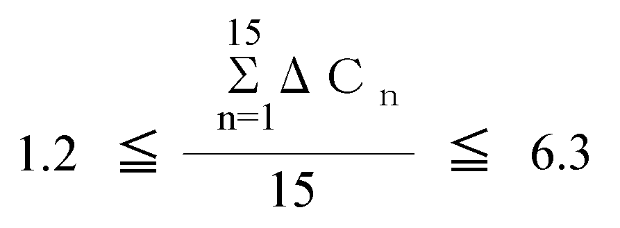
- 請求項46に記載の発光装置であって、前記飽和度差ΔCnが
-3.4 ≦ ΔCn ≦ 16.8 (nは1から15の自然数)
を満たすことを特徴とする発光装置。 - 請求項46に記載の発光装置であって、前記飽和度差の最大値と、前記飽和度差の最小値との間の差ΔCmax-ΔCminが
3.2 ≦ (ΔCmax-ΔCmin) ≦ 17.8
を満たすことを特徴とする発光装置。 - 請求項44~51のいずれか1項に記載の発光装置であって、
前記発光装置から当該放射方向に出射される光は、黒体放射軌跡からの距離DUVSSLが
-0.0250 ≦ DuvSSL ≦ -0.0100
を満たすことを特徴とする発光装置。 - 請求項44~52のいずれか1項に記載の発光装置であって、前記数式(3)または(4)で表される指標Acgが
-322 ≦ Acg ≦ -12
を満たすことを特徴とする発光装置。 - 請求項44~53のいずれか1項に記載の発光装置であって、
前記発光装置から当該放射方向に出射される光は、分光分布φSSL(λ)から導出される波長380nm以上780nm以下の範囲の放射効率K(lm/W)が、
206(lm/W) ≦ K(lm/W) ≦ 288(lm/W)
を満たすことを特徴とする発光装置。 - 請求項44~54のいずれか1項に記載の発光装置であって、前記相関色温度TSSL(K)が
2550(K) ≦ TSSL(K) ≦ 5650(K)
を満たすことを特徴とする発光装置。 - 請求項44~55のいずれか1項に記載の発光装置であって、前記発光装置から当該放射方向に出射される光が対象物を照明する照度が150lx以上5000lx以下であることを特徴とする発光装置。
- 請求項44~56のいずれか1項に記載の発光装置であって、前記発光装置は、前記半導体発光素子が出射する光を含めて1種類以上6種類以下の発光要素から出射される光を当該放射方向に発することを特徴とする発光装置。
- 請求項44~57のいずれか1項に記載の発光装置であって、前記半導体発光素子の発光スペクトルのピーク波長が380nm以上495nm未満であって、かつ、半値全幅が2nm以上45nm以下であることを特徴とする発光装置。
- 請求項58に記載の発光装置であって、前記半導体発光素子の発光スペクトルのピーク波長が395nm以上420nm未満であることを特徴とする発光装置。
- 請求項58に記載の発光装置であって、前記半導体発光素子の発光スペクトルのピーク波長が420nm以上455nm未満であることを特徴とする発光装置。
- 請求項58に記載の発光装置であって、当該半導体発光素子の発光スペクトルのピーク波長が455nm以上485nm未満であることを特徴とする発光装置。
- 請求項44~57のいずれか1項に記載の発光装置であって、前記半導体発光素子の発光スペクトルのピーク波長が495nm以上590nm未満であって、かつ、半値全幅が2nm以上75nm以下であることを特徴とする発光装置。
- 請求項44~57のいずれか1項に記載の発光装置であって、前記半導体発光素子の発光スペクトルのピーク波長が590nm以上780nm未満であって、かつ、半値全幅が2nm以上30nm以下であることを特徴とする発光装置。
- 請求項44~63のいずれか1項に記載の発光装置であって、前記半導体発光素子はサファイア基板、GaN基板、GaAs基板、GaP基板からなる群から選択されるいずれかの基板上で作成されたことを特徴とする発光装置。
- 請求項44~63のいずれか1項に記載の発光装置であって、前記半導体発光素子はGaN基板、またはGaP基板上で作成され、かつ前記基板の厚みが100μm以上2mm以下であることを特徴とする発光装置。
- 請求項44~63のいずれか1項に記載の発光装置であって、前記半導体発光素子はサファイア基板、またはGaAs基板上で作成され、かつ半導体発光素子は基板から剥離されてなることを特徴とする発光装置。
- 請求項44~66のいずれか1項に記載の発光装置であって、発光要素として蛍光体を備えることを特徴とする発光装置。
- 請求項67に記載の発光装置であって、前記蛍光体は、発光スペクトルの異なる蛍光体を1種類以上5種類以下含むことを特徴とする発光装置。
- 請求項67または請求項68に記載の発光装置であって、前記蛍光体は、室温で光励起した場合の単体発光スペクトルのピーク波長が380nm以上495nm未満であって、かつ、半値全幅が2nm以上90nm以下である蛍光体を含むことを特徴とする発光装置。
- 請求項69に記載の発光装置であって、前記蛍光体が下記一般式(5)で表される蛍光体、下記一般式(5)´で表される蛍光体、(Sr,Ba)3MgSi2O8:Eu2+、および(Ba,Sr,Ca,Mg)Si2O2N2:Euからなる群から選択される1種以上を含むことを特徴とする発光装置。
(Ba、Sr、Ca)MgAl10O17:Mn,Eu (5)
SraBabEux(PO4)cXd (5)´
(一般式(5)´において、XはClである。また、c、d及びxは、2.7≦c≦3.3、0.9≦d≦1.1、0.3≦x≦1.2を満足する数である。さらに、a及びbは、a+b=5-xかつ0≦b/(a+b)≦0.6の条件を満足する。) - 請求項67または請求項68に記載の発光装置であって、前記蛍光体は、室温で光励起した場合の単体発光スペクトルのピーク波長が495nm以上590nm未満であって、かつ、半値全幅が2nm以上130nm以下である蛍光体を含むことを特徴とする発光装置。
- 請求項71に記載の発光装置であって、前記蛍光体がSi6-zAlzOzN8-z:Eu(ただし0<z<4.2)、下記一般式(6)で表される蛍光体、下記一般式(6)´で表される蛍光体、およびSrGaS4:Eu2+からなる群から選択される1種以上を含むことを特徴とする発光装置。
(BaaCabSrcMgdEux)SiO4 (6)
(一般式(6)においてa、b、c、dおよびxが、a+b+c+d+x=2、1.0 ≦ a ≦ 2.0、0 ≦ b < 0.2、0.2 ≦ c ≦ 0.8、0 ≦ d < 0.2および0 < x ≦ 0.5を満たす。)
Ba1-x-y SrxEuy Mg1-z Mnz Al10O17 (6)´
(一般式(6)´においてx、yおよびzはそれぞれ0.1≦x≦0.4、0.25≦y≦0.6及び0.05≦z≦0.5を満たす。) - 請求項67または請求項68に記載の発光装置であって、前記蛍光体は、室温で光励起した場合の単体発光スペクトルのピーク波長が590nm以上780nm未満であって、かつ、半値全幅が2nm以上130nm以下である蛍光体を含むことを特徴とする発光装置。
- 請求項73に記載の発光装置であって、前記蛍光体が下記一般式(7)で表される蛍光体、下記一般式(7)´で表される蛍光体、(Sr,Ca,Ba)2AlxSi5-xOxN8-x:Eu(ただし0≦x≦2)、Euy(Sr,Ca,Ba)1-y:Al1+xSi4-xOxN7-x(ただし0≦x<4、0≦y<0.2)、K2SiF6:Mn4+、A2+xMyMnzFn(AはNaおよび/またはK;MはSiおよびAl;-1≦x≦1かつ0.9≦y+z≦1.1かつ0.001≦z≦0.4かつ5≦n≦7)、(Ca,Sr,Ba,Mg)AlSiN3:Euおよび/または(Ca,Sr,Ba)AlSiN3:Eu、並びに(CaAlSiN3)1-x(Si2N2O)x:Eu(ただし、xは0<x<0.5)からなる群から選択される1種以上を含むことを特徴とする発光装置。
(La1-x-y,Eux,Lny)2O2S (7)
(一般式(7)において、x及びyはそれぞれ0.02≦x≦0.50及び0≦y≦0.50を満たす数を表し、LnはY、Gd、Lu、Sc、Sm及びErの少なくとも1種の3価希土類元素を表す。)
(k-x)MgO・xAF2・GeO2:yMn4+ (7)´
(一般式(7)´において、k、x、yは、各々、2.8≦k≦5、0.1≦x≦0.7、0.005≦y≦0.015を満たす数を表し、Aはカルシウム(Ca)、ストロンチウム(Sr)、バリウム(Ba)、亜鉛(Zn)、またはこれらの混合物である。) - 請求項44~57のいずれか1項に記載の発光装置であって、発光要素として蛍光体を備え、前記半導体発光素子は発光スペクトルのピーク波長が395nm以上420nm未満であり、前記蛍光体は、SBCA、β-SiAlON、およびCASONを含むことを特徴とする発光装置。
- 請求項44~57のいずれか1項に記載の発光装置であって、発光要素として蛍光体を備え、前記半導体発光素子は発光スペクトルのピーク波長が395nm以上420nm未満であり、前記蛍光体は、SCA、β-SiAlON、およびCASONを含むことを特徴とする発光装置。
- 請求項44~76のいずれか1項に記載の発光装置であって、パッケージ化LED、LEDモジュール、LED照明器具、およびLED照明システムからなる群から選択されるいずれかであることを特徴とする発光装置。
- 家庭用照明装置として用いられる、請求項44~77のいずれか1項に記載の発光装置。
- 展示物用照明装置として用いられる、請求項44~77のいずれか1項に記載の発光装置。
- 演出用照明装置として用いられる、請求項44~77のいずれか1項に記載の発光装置。
- 医療用照明装置として用いられる、請求項44~77のいずれか1項に記載の発光装置。
- 作業用照明装置として用いられる、請求項44~77のいずれか1項に記載の発光装置。
- 工業機器内用照明装置として用いられる、請求項44~77のいずれか1項に記載の発光装置。
- 交通機関内装用照明装置として用いられる、請求項44~77のいずれか1項に記載の発光装置。
- 美術品用照明装置として用いられる、請求項44~77のいずれか1項に記載の発光装置。
- 高齢者用照明装置として用いられる、請求項44~77のいずれか1項に記載の発光装置。
- 少なくとも半導体発光素子を発光要素として備える発光装置の設計方法であって、
前記発光装置から出射される光が、ANSI C78.377で定義される黒体放射軌跡からの距離DUVSSLが-0.0350 ≦ DuvSSL ≦ -0.0040である光を、主たる放射方向に含むようにし、
かつ、
前記発光装置から当該放射方向に出射される光の分光分布をφSSL(λ)、前記発光装置から当該放射方向に出射される光のTSSL(K)に応じて選択される基準の光の分光分布をφref(λ)、前記発光装置から当該放射方向に出射される光の三刺激値を(XSSL、YSSL、ZSSL)、前記発光装置から当該放射方向に出射される光のTSSL(K)に応じて選択される基準の光の三刺激値を(Xref、Yref、Zref)とし、
前記発光装置から当該放射方向に出射される光の規格化分光分布SSSL(λ)と、前記発光装置から当該放射方向に出射される光のTSSL(K)に応じて選択される基準の光の規格化分光分布Sref(λ)と、これら規格化分光分布の差ΔS(λ)をそれぞれ、
SSSL(λ)=φSSL(λ)/YSSL
Sref(λ)=φref(λ)/Yref
ΔS(λ)=Sref(λ)-SSSL(λ)
と定義し、
波長380nm以上780nm以内の範囲で、SSSL(λ)の最長波長極大値を与える波長をλR(nm)とした際に、λRよりも長波長側にSSSL(λR)/2となる波長Λ4が存在し、
下記数式(3)で表される指標Acgが、-360 ≦ Acg ≦ -10となるように調整することを特徴とする発光装置の設計方法。

- 少なくとも半導体発光素子を発光要素として備える発光装置の設計方法であって、
前記発光装置から出射される光が、ANSI C78.377で定義される黒体放射軌跡からの距離DUVSSLが-0.0350 ≦ DuvSSL ≦ -0.0040である光を、主たる放射方向に含むようにし、
かつ、
前記発光装置から当該放射方向に出射される光の分光分布をφSSL(λ)、前記発光装置から当該放射方向に出射される光のTSSL(K)に応じて選択される基準の光の分光分布をφref(λ)、前記発光装置から当該放射方向に出射される光の三刺激値を(XSSL、YSSL、ZSSL)、前記発光装置から当該放射方向に出射される光のTSSL(K)に応じて選択される基準の光の三刺激値を(Xref、Yref、Zref)とし、
前記発光装置から当該放射方向に出射される光の規格化分光分布SSSL(λ)と、前記発光装置から当該放射方向に出射される光のTSSL(K)に応じて選択される基準の光の規格化分光分布Sref(λ)と、これら規格化分光分布の差ΔS(λ)をそれぞれ、
SSSL(λ)=φSSL(λ)/YSSL
Sref(λ)=φref(λ)/Yref
ΔS(λ)=Sref(λ)-SSSL(λ)
と定義し、
波長380nm以上780nm以内の範囲で、SSSL(λ)の最長波長極大値を与える波長をλR(nm)とした際に、λRよりも長波長側にSSSL(λR)/2となる波長Λ4が存在せず、
下記数式(4)で表される指標Acgが、-360 ≦ Acg ≦ -10となるように調整することを特徴とする発光装置の設計方法。

Priority Applications (8)
| Application Number | Priority Date | Filing Date | Title |
|---|---|---|---|
| EP19180488.9A EP3565383A1 (en) | 2011-09-02 | 2012-08-31 | Illumination method and light-emitting device |
| EP12827647.4A EP2753151A4 (en) | 2011-09-02 | 2012-08-31 | LIGHTING METHOD AND LIGHT EMITTING DEVICE |
| CN201280005125.2A CN103299718B (zh) | 2011-09-02 | 2012-08-31 | 照明方法和发光装置 |
| US14/196,617 US9373757B2 (en) | 2011-09-02 | 2014-03-04 | Illumination method and light-emitting device |
| US14/927,703 US9478714B2 (en) | 2011-09-02 | 2015-10-30 | Illumination method and light-emitting device |
| US15/258,155 US9722150B2 (en) | 2011-09-02 | 2016-09-07 | Illumination method and light-emitting device |
| US15/494,664 US9954149B2 (en) | 2011-09-02 | 2017-04-24 | Illumination method and light-emitting device |
| US15/911,269 US10355177B2 (en) | 2011-09-02 | 2018-03-05 | Illumination method and light-emitting device |
Applications Claiming Priority (6)
| Application Number | Priority Date | Filing Date | Title |
|---|---|---|---|
| JP2011-192142 | 2011-09-02 | ||
| JP2011192142 | 2011-09-02 | ||
| JP2011-192140 | 2011-09-02 | ||
| JP2011192140 | 2011-09-02 | ||
| JP2011223472 | 2011-10-07 | ||
| JP2011-223472 | 2011-10-07 |
Related Child Applications (1)
| Application Number | Title | Priority Date | Filing Date |
|---|---|---|---|
| US14/196,617 Continuation US9373757B2 (en) | 2011-09-02 | 2014-03-04 | Illumination method and light-emitting device |
Publications (1)
| Publication Number | Publication Date |
|---|---|
| WO2013031943A1 true WO2013031943A1 (ja) | 2013-03-07 |
Family
ID=47756419
Family Applications (1)
| Application Number | Title | Priority Date | Filing Date |
|---|---|---|---|
| PCT/JP2012/072144 WO2013031943A1 (ja) | 2011-09-02 | 2012-08-31 | 照明方法及び発光装置 |
Country Status (5)
| Country | Link |
|---|---|
| US (5) | US9373757B2 (ja) |
| EP (2) | EP2753151A4 (ja) |
| JP (7) | JP5257538B2 (ja) |
| CN (2) | CN103299718B (ja) |
| WO (1) | WO2013031943A1 (ja) |
Cited By (3)
| Publication number | Priority date | Publication date | Assignee | Title |
|---|---|---|---|---|
| WO2018155665A1 (ja) | 2017-02-27 | 2018-08-30 | シチズン電子株式会社 | 半導体発光装置及び照明装置 |
| CN110832244A (zh) * | 2017-04-20 | 2020-02-21 | 西铁城电子株式会社 | 对展示有展示物的空间进行照明的照明系统和照明方法 |
| US11003052B2 (en) | 2016-10-17 | 2021-05-11 | Citizen Electronics Co., Ltd. | Mobile device |
Families Citing this family (33)
| Publication number | Priority date | Publication date | Assignee | Title |
|---|---|---|---|---|
| CN103299718B (zh) | 2011-09-02 | 2015-12-23 | 西铁城电子株式会社 | 照明方法和发光装置 |
| CN103299719B (zh) | 2011-09-02 | 2014-10-22 | 三菱化学株式会社 | 照明方法和发光装置 |
| WO2014136748A1 (ja) | 2013-03-04 | 2014-09-12 | 三菱化学株式会社 | 発光装置、発光装置の設計方法、発光装置の駆動方法、照明方法、および発光装置の製造方法 |
| AU2014248104B2 (en) * | 2013-04-04 | 2018-07-05 | Circadian Zirclight Inc | Lighting systems for protecting circadian neuroendocrine function |
| ITUD20130104A1 (it) * | 2013-08-08 | 2015-02-09 | Martini Spa | Sorgente luminosa a luce piacevole |
| US9745511B2 (en) * | 2013-08-08 | 2017-08-29 | Merck Patent Gmbh | Phosphors |
| CN111554790B (zh) * | 2013-12-27 | 2023-09-15 | 西铁城电子株式会社 | 发光装置的设计方法 |
| JP6356005B2 (ja) * | 2013-12-27 | 2018-07-11 | シチズン電子株式会社 | 発光装置及び発光装置の設計方法 |
| CN105849920B (zh) * | 2013-12-27 | 2020-11-06 | 西铁城电子株式会社 | 发光装置和发光装置的设计方法 |
| JP6666064B2 (ja) * | 2014-09-03 | 2020-03-13 | シチズン電子株式会社 | 半導体発光素子を含む発光装置、および照明方法 |
| JP6356018B2 (ja) * | 2014-09-03 | 2018-07-11 | シチズン電子株式会社 | 発光装置及び発光装置の製造方法 |
| JP6349771B2 (ja) * | 2014-02-21 | 2018-07-04 | サンケン電気株式会社 | 照明装置 |
| US9929319B2 (en) * | 2014-06-13 | 2018-03-27 | General Electric Company | LED package with red-emitting phosphors |
| US10918747B2 (en) | 2015-07-30 | 2021-02-16 | Vital Vio, Inc. | Disinfecting lighting device |
| US10357582B1 (en) | 2015-07-30 | 2019-07-23 | Vital Vio, Inc. | Disinfecting lighting device |
| JP2018525848A (ja) | 2015-07-30 | 2018-09-06 | バイタル バイオ、 インコーポレイテッド | 単一ダイオード殺菌 |
| WO2017131697A1 (en) * | 2016-01-28 | 2017-08-03 | Ecosense Lighting Inc | Systems for providing tunable white light with high color rendering |
| DE212017000060U1 (de) | 2016-02-03 | 2018-09-10 | Opple Lighting Co., Ltd. | Lichtquellenmodul und Beleuchtungsvorrichtung |
| EP3249703B1 (en) * | 2016-05-26 | 2021-08-04 | Nichia Corporation | Light emitting device |
| DE102017108190A1 (de) * | 2017-04-18 | 2018-10-31 | Osram Opto Semiconductors Gmbh | Strahlungsemittierendes optoelektronisches Bauelement |
| KR102373817B1 (ko) | 2017-05-02 | 2022-03-14 | 삼성전자주식회사 | 백색 발광장치 및 조명 장치 |
| CN108022920A (zh) * | 2017-11-10 | 2018-05-11 | 江苏稳润光电科技有限公司 | 一种可双面发光的生鲜灯led光源的制作方法 |
| US10617774B2 (en) | 2017-12-01 | 2020-04-14 | Vital Vio, Inc. | Cover with disinfecting illuminated surface |
| US10413626B1 (en) | 2018-03-29 | 2019-09-17 | Vital Vio, Inc. | Multiple light emitter for inactivating microorganisms |
| US11639897B2 (en) | 2019-03-29 | 2023-05-02 | Vyv, Inc. | Contamination load sensing device |
| US11541135B2 (en) | 2019-06-28 | 2023-01-03 | Vyv, Inc. | Multiple band visible light disinfection |
| US11369704B2 (en) | 2019-08-15 | 2022-06-28 | Vyv, Inc. | Devices configured to disinfect interiors |
| JP7149602B2 (ja) * | 2019-08-19 | 2022-10-07 | 株式会社ユニバーサルエンターテインメント | 遊技機 |
| US11878084B2 (en) | 2019-09-20 | 2024-01-23 | Vyv, Inc. | Disinfecting light emitting subcomponent |
| JPWO2021085546A1 (ja) * | 2019-10-30 | 2021-05-06 | ||
| CN110859159B (zh) * | 2019-12-05 | 2021-09-21 | 中国水产科学研究院南海水产研究所 | 一种陆架区海底巡航式分类采样装置及其使用方法 |
| CN114916109B (zh) * | 2022-05-20 | 2023-09-26 | 苏州汉瑞森光电科技股份有限公司 | 一种均匀发光车用后位置灯的角度识别方法及系统 |
| US20240057239A1 (en) * | 2022-08-15 | 2024-02-15 | Alliance Sports Group, L.P. | Lighting Device |
Citations (4)
| Publication number | Priority date | Publication date | Assignee | Title |
|---|---|---|---|---|
| JP3503139B2 (ja) | 1996-07-29 | 2004-03-02 | 日亜化学工業株式会社 | 発光装置と表示装置 |
| JP2009048989A (ja) * | 2007-07-20 | 2009-03-05 | Toshiba Lighting & Technology Corp | 照明装置 |
| JP2009099510A (ja) * | 2007-02-15 | 2009-05-07 | Toshiba Lighting & Technology Corp | 照明装置 |
| WO2010126065A1 (ja) * | 2009-04-27 | 2010-11-04 | 東芝ライテック株式会社 | 照明装置 |
Family Cites Families (49)
| Publication number | Priority date | Publication date | Assignee | Title |
|---|---|---|---|---|
| JPS503139B1 (ja) | 1970-08-12 | 1975-01-31 | ||
| JPS515016B2 (ja) | 1973-05-12 | 1976-02-17 | ||
| US5803579A (en) | 1996-06-13 | 1998-09-08 | Gentex Corporation | Illuminator assembly incorporating light emitting diodes |
| JP3424566B2 (ja) | 1998-09-29 | 2003-07-07 | 松下電器産業株式会社 | 蛍光ランプおよび照明器具 |
| US6577073B2 (en) | 2000-05-31 | 2003-06-10 | Matsushita Electric Industrial Co., Ltd. | Led lamp |
| JP2002057376A (ja) * | 2000-05-31 | 2002-02-22 | Matsushita Electric Ind Co Ltd | Ledランプ |
| US7453195B2 (en) | 2004-08-02 | 2008-11-18 | Lumination Llc | White lamps with enhanced color contrast |
| US20070241657A1 (en) | 2004-08-02 | 2007-10-18 | Lumination, Llc | White light apparatus with enhanced color contrast |
| JP2006269448A (ja) * | 2005-03-22 | 2006-10-05 | Stanley Electric Co Ltd | Led |
| JP4890152B2 (ja) * | 2005-11-08 | 2012-03-07 | シャープ株式会社 | 発光装置 |
| JP2007141737A (ja) | 2005-11-21 | 2007-06-07 | Sharp Corp | 照明装置、液晶表示装置、照明装置の制御方法、照明装置制御プログラム、および記録媒体 |
| JP2007299714A (ja) | 2006-05-08 | 2007-11-15 | Osram-Melco Ltd | 照明器具 |
| JP2008041842A (ja) * | 2006-08-03 | 2008-02-21 | Sharp Corp | 半導体発光装置および半導体発光装置の製造方法 |
| JP2008081831A (ja) * | 2006-09-29 | 2008-04-10 | Mitsubishi Chemicals Corp | 基体表面処理方法、固形物、蛍光体含有組成物、発光装置、画像表示装置、および照明装置 |
| JP2008112811A (ja) | 2006-10-30 | 2008-05-15 | Kyocera Corp | 発光装置の製造方法 |
| KR100926898B1 (ko) * | 2007-02-16 | 2009-11-17 | 삼성전자주식회사 | 심적색 형광체 및 이의 제조 방법 |
| WO2008142622A1 (en) * | 2007-05-22 | 2008-11-27 | Koninklijke Philips Electronics N.V. | Personalized dimming controller |
| US7759854B2 (en) * | 2007-05-30 | 2010-07-20 | Global Oled Technology Llc | Lamp with adjustable color |
| JP2009060094A (ja) * | 2007-08-08 | 2009-03-19 | Toshiba Lighting & Technology Corp | 照明装置 |
| JP2009065145A (ja) * | 2007-08-10 | 2009-03-26 | Mitsubishi Chemicals Corp | 半導体発光装置、バックライトおよびカラー画像表示装置 |
| WO2009041171A1 (ja) | 2007-09-26 | 2009-04-02 | Toshiba Lighting & Technology Corporation | 照明装置 |
| US8247959B2 (en) * | 2007-10-17 | 2012-08-21 | General Electric Company | Solid state illumination system with improved color quality |
| US8373338B2 (en) | 2008-10-22 | 2013-02-12 | General Electric Company | Enhanced color contrast light source at elevated color temperatures |
| WO2009063915A1 (ja) | 2007-11-12 | 2009-05-22 | Mitsubishi Chemical Corporation | 照明装置 |
| US8733949B2 (en) | 2007-12-24 | 2014-05-27 | Columbia Insurance Company | System for representing colors including an integrating light capsule |
| US7990045B2 (en) * | 2008-03-15 | 2011-08-02 | Sensor Electronic Technology, Inc. | Solid-state lamps with partial conversion in phosphors for rendering an enhanced number of colors |
| JP2010232529A (ja) | 2009-03-27 | 2010-10-14 | Toyoda Gosei Co Ltd | 発光装置及びバックライト装置 |
| JP5462535B2 (ja) | 2009-06-25 | 2014-04-02 | パナソニック株式会社 | 照明装置 |
| JP2011029497A (ja) * | 2009-07-28 | 2011-02-10 | Mitsubishi Chemicals Corp | 白色発光装置およびそれを用いた照明装置 |
| EP2432037B1 (en) | 2009-08-26 | 2019-05-22 | Mitsubishi Chemical Corporation | Semiconductor white light-emitting device |
| US8258722B2 (en) | 2009-09-24 | 2012-09-04 | Cree, Inc. | Lighting device with defined spectral power distribution |
| JP5824676B2 (ja) | 2009-09-29 | 2015-11-25 | パナソニックIpマネジメント株式会社 | Led照明光源及び照明装置 |
| TW201115788A (en) * | 2009-10-30 | 2011-05-01 | Kingbright Electronics Co Ltd | Improved white light LED lighting device |
| CA2783741C (en) | 2009-12-09 | 2017-05-02 | Koninklijke Philips Electronics N.V. | Light system for emphasizing objects |
| US8466611B2 (en) * | 2009-12-14 | 2013-06-18 | Cree, Inc. | Lighting device with shaped remote phosphor |
| BR112012018512A2 (pt) * | 2010-01-28 | 2019-06-18 | Koninl Philips Electronics Nv | método para o controle de uma fonte de luz de cor ajustavável configurada para iluminar um objeto e sistema para o controle de uma fonte de luz de cor ajustável. |
| JP2011159809A (ja) * | 2010-02-01 | 2011-08-18 | Mitsubishi Chemicals Corp | 白色発光装置 |
| US20120281155A1 (en) * | 2010-02-17 | 2012-11-08 | Sharp Kabushiki Kaisha | Light source unit, lighting device, display device and television receiver |
| JP2011171590A (ja) * | 2010-02-19 | 2011-09-01 | Citizen Electronics Co Ltd | 発光ダイオード |
| JP2011181579A (ja) | 2010-02-26 | 2011-09-15 | Panasonic Corp | 発光装置、及びこれを用いた照明光源、表示装置ならびに電子機器 |
| CN102686700B (zh) | 2010-02-26 | 2015-03-25 | 三菱化学株式会社 | 卤磷酸盐荧光体及白色发光装置 |
| US20120267999A1 (en) | 2010-02-26 | 2012-10-25 | Mitsubishi Chemical Corporation | Halophosphate phosphor and white light-emitting device |
| JP2012060097A (ja) | 2010-06-25 | 2012-03-22 | Mitsubishi Chemicals Corp | 白色半導体発光装置 |
| WO2012050199A1 (ja) | 2010-10-15 | 2012-04-19 | 三菱化学株式会社 | 白色発光装置及び照明器具 |
| JP5654328B2 (ja) | 2010-11-24 | 2015-01-14 | パナソニックIpマネジメント株式会社 | 発光装置 |
| EP2468416A1 (de) | 2010-12-24 | 2012-06-27 | Sika Technology AG | Applikationsvorrichtung für Mehrkomponentenstoffe, ein Kartuschenset und eine Verpackungseinheit |
| JP5843698B2 (ja) | 2011-06-03 | 2016-01-13 | シチズン電子株式会社 | 半導体発光装置、展示物照射用照明装置、肉照射用照明装置、野菜照射用照明装置、鮮魚照射用照明装置、一般用照明装置、および半導体発光システム |
| CN103299718B (zh) | 2011-09-02 | 2015-12-23 | 西铁城电子株式会社 | 照明方法和发光装置 |
| CN103299719B (zh) * | 2011-09-02 | 2014-10-22 | 三菱化学株式会社 | 照明方法和发光装置 |
-
2012
- 2012-08-31 CN CN201280005125.2A patent/CN103299718B/zh active Active
- 2012-08-31 CN CN201510756038.6A patent/CN105357796B/zh active Active
- 2012-08-31 WO PCT/JP2012/072144 patent/WO2013031943A1/ja unknown
- 2012-08-31 EP EP12827647.4A patent/EP2753151A4/en not_active Ceased
- 2012-08-31 EP EP19180488.9A patent/EP3565383A1/en active Pending
- 2012-08-31 JP JP2012191022A patent/JP5257538B2/ja active Active
-
2013
- 2013-04-18 JP JP2013087055A patent/JP5964269B2/ja active Active
-
2014
- 2014-03-04 US US14/196,617 patent/US9373757B2/en active Active
- 2014-07-14 JP JP2014143970A patent/JP6038083B2/ja active Active
-
2015
- 2015-10-30 US US14/927,703 patent/US9478714B2/en active Active
-
2016
- 2016-06-29 JP JP2016128778A patent/JP6190005B2/ja active Active
- 2016-09-07 US US15/258,155 patent/US9722150B2/en active Active
-
2017
- 2017-04-24 US US15/494,664 patent/US9954149B2/en active Active
- 2017-08-03 JP JP2017151030A patent/JP6363277B2/ja active Active
-
2018
- 2018-03-05 US US15/911,269 patent/US10355177B2/en active Active
- 2018-06-27 JP JP2018121511A patent/JP6530113B2/ja active Active
-
2019
- 2019-05-15 JP JP2019091951A patent/JP6811804B2/ja active Active
Patent Citations (4)
| Publication number | Priority date | Publication date | Assignee | Title |
|---|---|---|---|---|
| JP3503139B2 (ja) | 1996-07-29 | 2004-03-02 | 日亜化学工業株式会社 | 発光装置と表示装置 |
| JP2009099510A (ja) * | 2007-02-15 | 2009-05-07 | Toshiba Lighting & Technology Corp | 照明装置 |
| JP2009048989A (ja) * | 2007-07-20 | 2009-03-05 | Toshiba Lighting & Technology Corp | 照明装置 |
| WO2010126065A1 (ja) * | 2009-04-27 | 2010-11-04 | 東芝ライテック株式会社 | 照明装置 |
Non-Patent Citations (3)
| Title |
|---|
| "General-purpose fluorescent light Meat-kun", 16 May 2011, PRINCE ELECTRIC CO.,LTD. |
| LEDS MAGAZINE, 22 August 2011 (2011-08-22), Retrieved from the Internet <URL:http://www.ledsmagazine.com/news/8/8/2> |
| See also references of EP2753151A4 |
Cited By (4)
| Publication number | Priority date | Publication date | Assignee | Title |
|---|---|---|---|---|
| US11003052B2 (en) | 2016-10-17 | 2021-05-11 | Citizen Electronics Co., Ltd. | Mobile device |
| WO2018155665A1 (ja) | 2017-02-27 | 2018-08-30 | シチズン電子株式会社 | 半導体発光装置及び照明装置 |
| CN110832244A (zh) * | 2017-04-20 | 2020-02-21 | 西铁城电子株式会社 | 对展示有展示物的空间进行照明的照明系统和照明方法 |
| CN110832244B (zh) * | 2017-04-20 | 2022-01-14 | 西铁城电子株式会社 | 对展示有展示物的空间进行照明的照明系统和照明方法 |
Also Published As
| Publication number | Publication date |
|---|---|
| CN105357796B (zh) | 2019-02-15 |
| JP2018186091A (ja) | 2018-11-22 |
| JP2013201132A (ja) | 2013-10-03 |
| US20140217417A1 (en) | 2014-08-07 |
| JP6038083B2 (ja) | 2016-12-07 |
| JP6363277B2 (ja) | 2018-07-25 |
| US10355177B2 (en) | 2019-07-16 |
| US20160072020A1 (en) | 2016-03-10 |
| US20180198036A1 (en) | 2018-07-12 |
| JP2013093311A (ja) | 2013-05-16 |
| CN103299718B (zh) | 2015-12-23 |
| US9478714B2 (en) | 2016-10-25 |
| JP6190005B2 (ja) | 2017-08-30 |
| US20160380163A1 (en) | 2016-12-29 |
| JP6811804B2 (ja) | 2021-01-13 |
| JP5964269B2 (ja) | 2016-08-03 |
| JP2018014331A (ja) | 2018-01-25 |
| US9373757B2 (en) | 2016-06-21 |
| US9954149B2 (en) | 2018-04-24 |
| JP6530113B2 (ja) | 2019-06-12 |
| JP2014225463A (ja) | 2014-12-04 |
| CN103299718A (zh) | 2013-09-11 |
| EP2753151A1 (en) | 2014-07-09 |
| JP5257538B2 (ja) | 2013-08-07 |
| EP3565383A1 (en) | 2019-11-06 |
| EP2753151A4 (en) | 2016-05-18 |
| JP2019149573A (ja) | 2019-09-05 |
| CN105357796A (zh) | 2016-02-24 |
| US20170229620A1 (en) | 2017-08-10 |
| JP2016186946A (ja) | 2016-10-27 |
| US9722150B2 (en) | 2017-08-01 |
Similar Documents
| Publication | Publication Date | Title |
|---|---|---|
| JP6363277B2 (ja) | 照明方法及び発光装置 | |
| JP6567112B2 (ja) | 照明方法及び発光装置 | |
| JP6584030B2 (ja) | 照明方法及び発光装置 | |
| WO2014136748A1 (ja) | 発光装置、発光装置の設計方法、発光装置の駆動方法、照明方法、および発光装置の製造方法 | |
| JP6820064B2 (ja) | 半導体発光素子を含む発光装置、発光装置の設計方法、発光装置の駆動方法、および照明方法 | |
| JP6462841B2 (ja) | 発光装置及び発光装置の製造方法 | |
| JP2018147895A (ja) | 発光装置及び発光装置の設計方法 | |
| JP2014170843A (ja) | Led照明装置 | |
| JP2014170853A (ja) | 発光装置及び照明方法 | |
| JP2014049319A (ja) | 発光装置及び照明方法 |
Legal Events
| Date | Code | Title | Description |
|---|---|---|---|
| 121 | Ep: the epo has been informed by wipo that ep was designated in this application |
Ref document number: 12827647 Country of ref document: EP Kind code of ref document: A1 |
|
| NENP | Non-entry into the national phase |
Ref country code: DE |