WO2013031828A1 - 電力変換装置 - Google Patents
電力変換装置 Download PDFInfo
- Publication number
- WO2013031828A1 WO2013031828A1 PCT/JP2012/071834 JP2012071834W WO2013031828A1 WO 2013031828 A1 WO2013031828 A1 WO 2013031828A1 JP 2012071834 W JP2012071834 W JP 2012071834W WO 2013031828 A1 WO2013031828 A1 WO 2013031828A1
- Authority
- WO
- WIPO (PCT)
- Prior art keywords
- axis
- magnetic flux
- power
- pulse
- switching element
- Prior art date
- Legal status (The legal status is an assumption and is not a legal conclusion. Google has not performed a legal analysis and makes no representation as to the accuracy of the status listed.)
- Ceased
Links
Images













Classifications
-
- B—PERFORMING OPERATIONS; TRANSPORTING
- B60—VEHICLES IN GENERAL
- B60L—PROPULSION OF ELECTRICALLY-PROPELLED VEHICLES; SUPPLYING ELECTRIC POWER FOR AUXILIARY EQUIPMENT OF ELECTRICALLY-PROPELLED VEHICLES; ELECTRODYNAMIC BRAKE SYSTEMS FOR VEHICLES IN GENERAL; MAGNETIC SUSPENSION OR LEVITATION FOR VEHICLES; MONITORING OPERATING VARIABLES OF ELECTRICALLY-PROPELLED VEHICLES; ELECTRIC SAFETY DEVICES FOR ELECTRICALLY-PROPELLED VEHICLES
- B60L3/00—Electric devices on electrically-propelled vehicles for safety purposes; Monitoring operating variables, e.g. speed, deceleration or energy consumption
- B60L3/0023—Detecting, eliminating, remedying or compensating for drive train abnormalities, e.g. failures within the drive train
- B60L3/003—Detecting, eliminating, remedying or compensating for drive train abnormalities, e.g. failures within the drive train relating to inverters
-
- B—PERFORMING OPERATIONS; TRANSPORTING
- B60—VEHICLES IN GENERAL
- B60L—PROPULSION OF ELECTRICALLY-PROPELLED VEHICLES; SUPPLYING ELECTRIC POWER FOR AUXILIARY EQUIPMENT OF ELECTRICALLY-PROPELLED VEHICLES; ELECTRODYNAMIC BRAKE SYSTEMS FOR VEHICLES IN GENERAL; MAGNETIC SUSPENSION OR LEVITATION FOR VEHICLES; MONITORING OPERATING VARIABLES OF ELECTRICALLY-PROPELLED VEHICLES; ELECTRIC SAFETY DEVICES FOR ELECTRICALLY-PROPELLED VEHICLES
- B60L15/00—Methods, circuits, or devices for controlling the traction-motor speed of electrically-propelled vehicles
- B60L15/02—Methods, circuits, or devices for controlling the traction-motor speed of electrically-propelled vehicles characterised by the form of the current used in the control circuit
- B60L15/025—Methods, circuits, or devices for controlling the traction-motor speed of electrically-propelled vehicles characterised by the form of the current used in the control circuit using field orientation; Vector control; Direct Torque Control [DTC]
-
- B—PERFORMING OPERATIONS; TRANSPORTING
- B60—VEHICLES IN GENERAL
- B60L—PROPULSION OF ELECTRICALLY-PROPELLED VEHICLES; SUPPLYING ELECTRIC POWER FOR AUXILIARY EQUIPMENT OF ELECTRICALLY-PROPELLED VEHICLES; ELECTRODYNAMIC BRAKE SYSTEMS FOR VEHICLES IN GENERAL; MAGNETIC SUSPENSION OR LEVITATION FOR VEHICLES; MONITORING OPERATING VARIABLES OF ELECTRICALLY-PROPELLED VEHICLES; ELECTRIC SAFETY DEVICES FOR ELECTRICALLY-PROPELLED VEHICLES
- B60L50/00—Electric propulsion with power supplied within the vehicle
- B60L50/10—Electric propulsion with power supplied within the vehicle using propulsion power supplied by engine-driven generators, e.g. generators driven by combustion engines
- B60L50/16—Electric propulsion with power supplied within the vehicle using propulsion power supplied by engine-driven generators, e.g. generators driven by combustion engines with provision for separate direct mechanical propulsion
-
- B—PERFORMING OPERATIONS; TRANSPORTING
- B60—VEHICLES IN GENERAL
- B60L—PROPULSION OF ELECTRICALLY-PROPELLED VEHICLES; SUPPLYING ELECTRIC POWER FOR AUXILIARY EQUIPMENT OF ELECTRICALLY-PROPELLED VEHICLES; ELECTRODYNAMIC BRAKE SYSTEMS FOR VEHICLES IN GENERAL; MAGNETIC SUSPENSION OR LEVITATION FOR VEHICLES; MONITORING OPERATING VARIABLES OF ELECTRICALLY-PROPELLED VEHICLES; ELECTRIC SAFETY DEVICES FOR ELECTRICALLY-PROPELLED VEHICLES
- B60L50/00—Electric propulsion with power supplied within the vehicle
- B60L50/40—Electric propulsion with power supplied within the vehicle using propulsion power supplied by capacitors
-
- B—PERFORMING OPERATIONS; TRANSPORTING
- B60—VEHICLES IN GENERAL
- B60L—PROPULSION OF ELECTRICALLY-PROPELLED VEHICLES; SUPPLYING ELECTRIC POWER FOR AUXILIARY EQUIPMENT OF ELECTRICALLY-PROPELLED VEHICLES; ELECTRODYNAMIC BRAKE SYSTEMS FOR VEHICLES IN GENERAL; MAGNETIC SUSPENSION OR LEVITATION FOR VEHICLES; MONITORING OPERATING VARIABLES OF ELECTRICALLY-PROPELLED VEHICLES; ELECTRIC SAFETY DEVICES FOR ELECTRICALLY-PROPELLED VEHICLES
- B60L50/00—Electric propulsion with power supplied within the vehicle
- B60L50/50—Electric propulsion with power supplied within the vehicle using propulsion power supplied by batteries or fuel cells
- B60L50/60—Electric propulsion with power supplied within the vehicle using propulsion power supplied by batteries or fuel cells using power supplied by batteries
- B60L50/61—Electric propulsion with power supplied within the vehicle using propulsion power supplied by batteries or fuel cells using power supplied by batteries by batteries charged by engine-driven generators, e.g. series hybrid electric vehicles
-
- H—ELECTRICITY
- H02—GENERATION; CONVERSION OR DISTRIBUTION OF ELECTRIC POWER
- H02P—CONTROL OR REGULATION OF ELECTRIC MOTORS, ELECTRIC GENERATORS OR DYNAMO-ELECTRIC CONVERTERS; CONTROLLING TRANSFORMERS, REACTORS OR CHOKE COILS
- H02P21/00—Arrangements or methods for the control of electric machines by vector control, e.g. by control of field orientation
- H02P21/50—Vector control arrangements or methods not otherwise provided for in H02P21/00- H02P21/36
-
- B—PERFORMING OPERATIONS; TRANSPORTING
- B60—VEHICLES IN GENERAL
- B60L—PROPULSION OF ELECTRICALLY-PROPELLED VEHICLES; SUPPLYING ELECTRIC POWER FOR AUXILIARY EQUIPMENT OF ELECTRICALLY-PROPELLED VEHICLES; ELECTRODYNAMIC BRAKE SYSTEMS FOR VEHICLES IN GENERAL; MAGNETIC SUSPENSION OR LEVITATION FOR VEHICLES; MONITORING OPERATING VARIABLES OF ELECTRICALLY-PROPELLED VEHICLES; ELECTRIC SAFETY DEVICES FOR ELECTRICALLY-PROPELLED VEHICLES
- B60L2210/00—Converter types
- B60L2210/40—DC to AC converters
-
- B—PERFORMING OPERATIONS; TRANSPORTING
- B60—VEHICLES IN GENERAL
- B60L—PROPULSION OF ELECTRICALLY-PROPELLED VEHICLES; SUPPLYING ELECTRIC POWER FOR AUXILIARY EQUIPMENT OF ELECTRICALLY-PROPELLED VEHICLES; ELECTRODYNAMIC BRAKE SYSTEMS FOR VEHICLES IN GENERAL; MAGNETIC SUSPENSION OR LEVITATION FOR VEHICLES; MONITORING OPERATING VARIABLES OF ELECTRICALLY-PROPELLED VEHICLES; ELECTRIC SAFETY DEVICES FOR ELECTRICALLY-PROPELLED VEHICLES
- B60L2220/00—Electrical machine types; Structures or applications thereof
- B60L2220/10—Electrical machine types
- B60L2220/14—Synchronous machines
-
- B—PERFORMING OPERATIONS; TRANSPORTING
- B60—VEHICLES IN GENERAL
- B60L—PROPULSION OF ELECTRICALLY-PROPELLED VEHICLES; SUPPLYING ELECTRIC POWER FOR AUXILIARY EQUIPMENT OF ELECTRICALLY-PROPELLED VEHICLES; ELECTRODYNAMIC BRAKE SYSTEMS FOR VEHICLES IN GENERAL; MAGNETIC SUSPENSION OR LEVITATION FOR VEHICLES; MONITORING OPERATING VARIABLES OF ELECTRICALLY-PROPELLED VEHICLES; ELECTRIC SAFETY DEVICES FOR ELECTRICALLY-PROPELLED VEHICLES
- B60L2240/00—Control parameters of input or output; Target parameters
- B60L2240/10—Vehicle control parameters
- B60L2240/36—Temperature of vehicle components or parts
-
- B—PERFORMING OPERATIONS; TRANSPORTING
- B60—VEHICLES IN GENERAL
- B60L—PROPULSION OF ELECTRICALLY-PROPELLED VEHICLES; SUPPLYING ELECTRIC POWER FOR AUXILIARY EQUIPMENT OF ELECTRICALLY-PROPELLED VEHICLES; ELECTRODYNAMIC BRAKE SYSTEMS FOR VEHICLES IN GENERAL; MAGNETIC SUSPENSION OR LEVITATION FOR VEHICLES; MONITORING OPERATING VARIABLES OF ELECTRICALLY-PROPELLED VEHICLES; ELECTRIC SAFETY DEVICES FOR ELECTRICALLY-PROPELLED VEHICLES
- B60L2240/00—Control parameters of input or output; Target parameters
- B60L2240/40—Drive Train control parameters
- B60L2240/52—Drive Train control parameters related to converters
- B60L2240/525—Temperature of converter or components thereof
-
- B—PERFORMING OPERATIONS; TRANSPORTING
- B60—VEHICLES IN GENERAL
- B60L—PROPULSION OF ELECTRICALLY-PROPELLED VEHICLES; SUPPLYING ELECTRIC POWER FOR AUXILIARY EQUIPMENT OF ELECTRICALLY-PROPELLED VEHICLES; ELECTRODYNAMIC BRAKE SYSTEMS FOR VEHICLES IN GENERAL; MAGNETIC SUSPENSION OR LEVITATION FOR VEHICLES; MONITORING OPERATING VARIABLES OF ELECTRICALLY-PROPELLED VEHICLES; ELECTRIC SAFETY DEVICES FOR ELECTRICALLY-PROPELLED VEHICLES
- B60L2240/00—Control parameters of input or output; Target parameters
- B60L2240/40—Drive Train control parameters
- B60L2240/52—Drive Train control parameters related to converters
- B60L2240/527—Voltage
-
- H—ELECTRICITY
- H10—SEMICONDUCTOR DEVICES; ELECTRIC SOLID-STATE DEVICES NOT OTHERWISE PROVIDED FOR
- H10W—GENERIC PACKAGES, INTERCONNECTIONS, CONNECTORS OR OTHER CONSTRUCTIONAL DETAILS OF DEVICES COVERED BY CLASS H10
- H10W72/00—Interconnections or connectors in packages
- H10W72/071—Connecting or disconnecting
- H10W72/073—Connecting or disconnecting of die-attach connectors
- H10W72/07351—Connecting or disconnecting of die-attach connectors characterised by changes in properties of the die-attach connectors during connecting
- H10W72/07354—Connecting or disconnecting of die-attach connectors characterised by changes in properties of the die-attach connectors during connecting changes in dispositions
-
- H—ELECTRICITY
- H10—SEMICONDUCTOR DEVICES; ELECTRIC SOLID-STATE DEVICES NOT OTHERWISE PROVIDED FOR
- H10W—GENERIC PACKAGES, INTERCONNECTIONS, CONNECTORS OR OTHER CONSTRUCTIONAL DETAILS OF DEVICES COVERED BY CLASS H10
- H10W72/00—Interconnections or connectors in packages
- H10W72/30—Die-attach connectors
- H10W72/341—Dispositions of die-attach connectors, e.g. layouts
- H10W72/347—Dispositions of multiple die-attach connectors
-
- H—ELECTRICITY
- H10—SEMICONDUCTOR DEVICES; ELECTRIC SOLID-STATE DEVICES NOT OTHERWISE PROVIDED FOR
- H10W—GENERIC PACKAGES, INTERCONNECTIONS, CONNECTORS OR OTHER CONSTRUCTIONAL DETAILS OF DEVICES COVERED BY CLASS H10
- H10W72/00—Interconnections or connectors in packages
- H10W72/50—Bond wires
- H10W72/531—Shapes of wire connectors
- H10W72/5363—Shapes of wire connectors the connected ends being wedge-shaped
-
- H—ELECTRICITY
- H10—SEMICONDUCTOR DEVICES; ELECTRIC SOLID-STATE DEVICES NOT OTHERWISE PROVIDED FOR
- H10W—GENERIC PACKAGES, INTERCONNECTIONS, CONNECTORS OR OTHER CONSTRUCTIONAL DETAILS OF DEVICES COVERED BY CLASS H10
- H10W72/00—Interconnections or connectors in packages
- H10W72/50—Bond wires
- H10W72/541—Dispositions of bond wires
- H10W72/5449—Dispositions of bond wires not being orthogonal to a side surface of the chip, e.g. fan-out arrangements
-
- H—ELECTRICITY
- H10—SEMICONDUCTOR DEVICES; ELECTRIC SOLID-STATE DEVICES NOT OTHERWISE PROVIDED FOR
- H10W—GENERIC PACKAGES, INTERCONNECTIONS, CONNECTORS OR OTHER CONSTRUCTIONAL DETAILS OF DEVICES COVERED BY CLASS H10
- H10W72/00—Interconnections or connectors in packages
- H10W72/90—Bond pads, in general
- H10W72/921—Structures or relative sizes of bond pads
- H10W72/926—Multiple bond pads having different sizes
-
- H—ELECTRICITY
- H10—SEMICONDUCTOR DEVICES; ELECTRIC SOLID-STATE DEVICES NOT OTHERWISE PROVIDED FOR
- H10W—GENERIC PACKAGES, INTERCONNECTIONS, CONNECTORS OR OTHER CONSTRUCTIONAL DETAILS OF DEVICES COVERED BY CLASS H10
- H10W90/00—Package configurations
- H10W90/701—Package configurations characterised by the relative positions of pads or connectors relative to package parts
- H10W90/751—Package configurations characterised by the relative positions of pads or connectors relative to package parts of bond wires
- H10W90/756—Package configurations characterised by the relative positions of pads or connectors relative to package parts of bond wires between a chip and a stacked lead frame, conducting package substrate or heat sink
-
- Y—GENERAL TAGGING OF NEW TECHNOLOGICAL DEVELOPMENTS; GENERAL TAGGING OF CROSS-SECTIONAL TECHNOLOGIES SPANNING OVER SEVERAL SECTIONS OF THE IPC; TECHNICAL SUBJECTS COVERED BY FORMER USPC CROSS-REFERENCE ART COLLECTIONS [XRACs] AND DIGESTS
- Y02—TECHNOLOGIES OR APPLICATIONS FOR MITIGATION OR ADAPTATION AGAINST CLIMATE CHANGE
- Y02T—CLIMATE CHANGE MITIGATION TECHNOLOGIES RELATED TO TRANSPORTATION
- Y02T10/00—Road transport of goods or passengers
- Y02T10/60—Other road transportation technologies with climate change mitigation effect
- Y02T10/62—Hybrid vehicles
-
- Y—GENERAL TAGGING OF NEW TECHNOLOGICAL DEVELOPMENTS; GENERAL TAGGING OF CROSS-SECTIONAL TECHNOLOGIES SPANNING OVER SEVERAL SECTIONS OF THE IPC; TECHNICAL SUBJECTS COVERED BY FORMER USPC CROSS-REFERENCE ART COLLECTIONS [XRACs] AND DIGESTS
- Y02—TECHNOLOGIES OR APPLICATIONS FOR MITIGATION OR ADAPTATION AGAINST CLIMATE CHANGE
- Y02T—CLIMATE CHANGE MITIGATION TECHNOLOGIES RELATED TO TRANSPORTATION
- Y02T10/00—Road transport of goods or passengers
- Y02T10/60—Other road transportation technologies with climate change mitigation effect
- Y02T10/64—Electric machine technologies in electromobility
-
- Y—GENERAL TAGGING OF NEW TECHNOLOGICAL DEVELOPMENTS; GENERAL TAGGING OF CROSS-SECTIONAL TECHNOLOGIES SPANNING OVER SEVERAL SECTIONS OF THE IPC; TECHNICAL SUBJECTS COVERED BY FORMER USPC CROSS-REFERENCE ART COLLECTIONS [XRACs] AND DIGESTS
- Y02—TECHNOLOGIES OR APPLICATIONS FOR MITIGATION OR ADAPTATION AGAINST CLIMATE CHANGE
- Y02T—CLIMATE CHANGE MITIGATION TECHNOLOGIES RELATED TO TRANSPORTATION
- Y02T10/00—Road transport of goods or passengers
- Y02T10/60—Other road transportation technologies with climate change mitigation effect
- Y02T10/70—Energy storage systems for electromobility, e.g. batteries
-
- Y—GENERAL TAGGING OF NEW TECHNOLOGICAL DEVELOPMENTS; GENERAL TAGGING OF CROSS-SECTIONAL TECHNOLOGIES SPANNING OVER SEVERAL SECTIONS OF THE IPC; TECHNICAL SUBJECTS COVERED BY FORMER USPC CROSS-REFERENCE ART COLLECTIONS [XRACs] AND DIGESTS
- Y02—TECHNOLOGIES OR APPLICATIONS FOR MITIGATION OR ADAPTATION AGAINST CLIMATE CHANGE
- Y02T—CLIMATE CHANGE MITIGATION TECHNOLOGIES RELATED TO TRANSPORTATION
- Y02T10/00—Road transport of goods or passengers
- Y02T10/60—Other road transportation technologies with climate change mitigation effect
- Y02T10/7072—Electromobility specific charging systems or methods for batteries, ultracapacitors, supercapacitors or double-layer capacitors
-
- Y—GENERAL TAGGING OF NEW TECHNOLOGICAL DEVELOPMENTS; GENERAL TAGGING OF CROSS-SECTIONAL TECHNOLOGIES SPANNING OVER SEVERAL SECTIONS OF THE IPC; TECHNICAL SUBJECTS COVERED BY FORMER USPC CROSS-REFERENCE ART COLLECTIONS [XRACs] AND DIGESTS
- Y02—TECHNOLOGIES OR APPLICATIONS FOR MITIGATION OR ADAPTATION AGAINST CLIMATE CHANGE
- Y02T—CLIMATE CHANGE MITIGATION TECHNOLOGIES RELATED TO TRANSPORTATION
- Y02T10/00—Road transport of goods or passengers
- Y02T10/60—Other road transportation technologies with climate change mitigation effect
- Y02T10/72—Electric energy management in electromobility
Definitions
- the present invention relates to a power conversion device that converts DC power into AC power or AC power into DC power.
- a power conversion device that receives direct current power and converts the direct current power into alternating current power for supplying to the rotating electrical machine includes a plurality of switching elements, and the switching element repeats a switching operation to supply the direct current supplied. Convert power to AC power. Many of the power converters are also used to convert AC power induced in the rotating electrical machine into DC power by the switching operation of the switching element.
- the above-described switching element is generally controlled based on a pulse width modulation method (hereinafter referred to as a PWM method) using a carrier wave that changes at a constant frequency. By increasing the frequency of the carrier wave, the control accuracy is improved and the torque generated by the rotating electrical machine tends to be smooth.
- Patent Document 1 An example of a power converter is disclosed in Japanese Patent Laid-Open No. 63-234878 (see Patent Document 1).
- the switching element increases power loss and heat generation when switching from the cut-off state to the conductive state or when switching from the conductive state to the cut-off state. To do. It is desirable to reduce the power loss of the switching element described above, and the amount of heat generated by the switching element can be reduced by reducing the power loss. For this purpose, it is desirable to reduce the number of switching times of the switching element.
- the frequency of the carrier wave is lowered in order to reduce the number of times of switching per unit time of the switching element, the distortion of the current output from the power converter increases, and the motor This leads to an increase in loss.
- an object of the present invention is to reduce switching loss and improve safety while suppressing increase in motor loss as much as possible in a power converter connected to a permanent magnet motor.
- the embodiment described below reflects research results preferable as a product, and solves various specific problems preferable as a product. Specific problems to be solved by specific configurations and operations in the following embodiments will be described in the following embodiments.
- the power converter according to the first aspect of the present invention is connected to a permanent magnet motor, and has a plurality of series circuits in which an upper arm switching element and a lower arm switching element are connected in series.
- the control circuit predicts the locus of the d-axis magnetic flux that is the d-axis component of the magnetic flux generated in the permanent magnet motor and the locus of the q-axis magnetic flux that is the q-axis component of the magnetic flux generated in the permanent magnet motor. Based on the prediction result, the state of the switching element is calculated so that the d-axis magnetic flux is within a predetermined d-axis magnetic flux fluctuation range and the q-axis magnetic flux is within a predetermined q-axis magnetic flux fluctuation range.
- the d axis is a coordinate axis defined along the main magnetic flux direction of the permanent magnet disposed in the rotor of the permanent magnet motor, and the q axis is defined along the direction orthogonal to the d axis. Coordinate axes.
- the control circuit outputs the voltage command signal of the rotating coordinate system defined by the d-axis and the q-axis based on the input information to a predetermined stationary state.
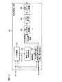
- a coordinate converter for converting to a voltage command signal in the coordinate system, and a voltage vector region corresponding to the voltage command signal based on the voltage command signal converted by the coordinate converter, and an output corresponding to the searched voltage vector region A voltage vector region searcher for determining a voltage vector, and a d-axis magnetic flux trajectory and a q-axis magnetic flux trajectory are predicted based on the output voltage vector determined by the voltage vector region searcher, and the predicted d-axis magnetic flux trajectory A predictor that compares the d-axis flux fluctuation range and the q-axis flux trajectory with the q-axis flux fluctuation range, respectively, and calculates the state of the switching element and the switching time.
- Ri based on the state and the switching time of the computed switching element, and a signal output for outputting a control signal, it is preferable to have a.
- the d-axis magnetic flux fluctuation range when the electric resistance value of the permanent magnet is smaller than the electric resistance value of the iron core of the rotor, the d-axis magnetic flux fluctuation range is q
- the d-axis magnetic flux fluctuation range is preferably set larger than the q-axis magnetic flux fluctuation range.
- a power converter is connected to a permanent magnet motor, and has a plurality of series circuits in which a switching element for an upper arm and a switching element for a lower arm are connected in series. Receiving the DC power, generating AC power, outputting the generated AC power to the permanent magnet motor, and repeatedly calculating the state of the switching element for each predetermined control cycle based on the input information, A control circuit that generates a control signal for controlling conduction or blocking of the switching element according to a calculation result, and a driver circuit that generates a drive signal for conducting or blocking the switching element based on the control signal from the control circuit, Have.
- the control circuit predicts a trajectory of the d-axis current that is the d-axis component of the current flowing through the permanent magnet motor and a trajectory of the q-axis current that is the q-axis component of the current flowing through the permanent magnet motor. Based on the prediction result, the state of the switching element is calculated so that the d-axis current falls within a predetermined d-axis current fluctuation range and the q-axis current falls within a predetermined q-axis current fluctuation range.
- the d axis is a coordinate axis defined along the main magnetic flux direction of the permanent magnet disposed in the rotor of the permanent magnet motor, and the q axis is defined along the direction orthogonal to the d axis. Coordinate axes.
- the control circuit outputs the voltage command signal of the rotating coordinate system defined by the d-axis and the q-axis based on the input information to a predetermined stationary state.
- a coordinate converter for converting to a voltage command signal in the coordinate system, and a voltage vector region corresponding to the voltage command signal based on the voltage command signal converted by the coordinate converter, and an output corresponding to the searched voltage vector region
- a voltage vector region searcher for determining a voltage vector, a d-axis current locus and a q-axis current locus are predicted based on the output voltage vector determined by the voltage vector region searcher, and the predicted d-axis current locus
- a predictor that compares the d-axis current fluctuation range and the q-axis current locus with the q-axis current fluctuation range to calculate the state of the switching element and the switching time.
- Ri based on the state and the switching time of the computed switching element, and a signal output for outputting a control signal, it is preferable to have a.
- the d-axis current fluctuation range when the electric resistance value of the permanent magnet is smaller than the electric resistance value of the iron core of the rotor, the d-axis current fluctuation range is q
- the axial current fluctuation range is set to be smaller and the electric resistance value of the permanent magnet is larger than the electric resistance value of the rotor core
- the d-axis current fluctuation range is preferably set to be larger than the q-axis current fluctuation range.
- an increase in motor loss can be suppressed to some extent in the power conversion device, and further switching loss can be reduced.
- FIG. 3 is a diagram illustrating a circuit configuration of an inverter circuit 140.
- FIG. It is an external appearance perspective view of the power converter device 200 as one embodiment of this invention. It is an external appearance perspective view of the power converter device 200 as one embodiment of this invention. It is a figure which shows the state which removed the lid
- FIG. 6 is a view showing a state where the housing 10 is removed from the flow path forming body 12 in FIG. 5.
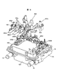
- 2 is an exploded perspective view of a power conversion device 200.
- FIG. 3 is an external perspective view in which a power module 300U to 300W, a capacitor module 500, and a bus bar assembly 800 are assembled to a flow path forming body 12.
- FIG. The state which removed the bus-bar assembly 800 from the flow-path formation body 12 is shown.
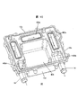
- 3 is a perspective view of a flow path forming body 12.
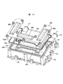
- FIG. It is the disassembled perspective view which looked at the flow-path formation body 12 from the back surface side.
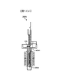
- FIG. 14 is a cross-sectional view of the power module 300U in the state shown in FIG. A cross-sectional view of the power module 300U before the fins 305 are pressurized and the curved portion 304A is deformed is shown. It is a perspective view which shows the state which removed the module case 304 from the power module 300U shown to Fig.13 (a) and FIG.13 (b). Similarly to FIGS. 12B and 13B, FIG. 14B is a cross-sectional view of the power module 300U in the state shown in FIG. FIG.
- FIG. 15 is a perspective view of a power module 300U in which the first sealing resin 348 and the wiring insulating portion 608 are further removed from the state shown in FIGS. 14 (a) and 14 (b). It is a figure for demonstrating the assembly process of the module primary sealing body 302.
- FIG. 1 is an external perspective view of a capacitor module 500.
- FIG. 2 is a perspective view of a bus bar assembly 800.
- FIG. FIG. 4 is a view showing a flow path forming body 12 in which power modules 300U to 300W are fixed to openings 402a to 402c and a capacitor module 500 is stored in a storage space 405.
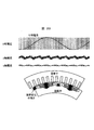
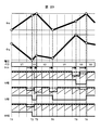
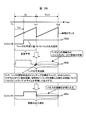
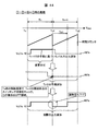
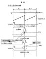
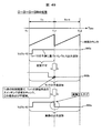
- FIG. 5 shows UVW three-phase voltage pulses, d-axis current ripple ⁇ Id, q-axis current ripple ⁇ Iq, and UVW three-phase phase currents when the modulation method according to the present invention is applied.
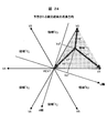
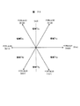
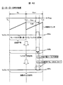
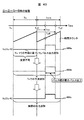
- the modulation system according to the present invention it is a conceptual diagram showing a method for determining a desired output voltage vector for a predetermined voltage command. It is the figure which showed the selection method of a command voltage vector and an output voltage vector, and the mode of the magnetic flux change at the time of the selection. It is the figure which showed the selection method of a command voltage vector and an output voltage vector, and the mode of the magnetic flux change at the time of the selection.
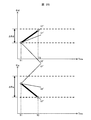
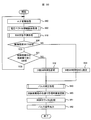
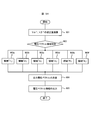
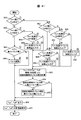
- FIG. 41 it is a figure which shows the example of a pulse waveform at the time of performing each process of step 941, 942, 943, and 944 in order.
- FIG. 42 is a diagram illustrating an example of a pulse waveform when the processes of steps 941, 942 and 943 are executed in order in the flowchart of FIG. 41 and the process of step 904 is not executed.
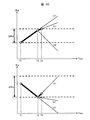
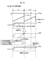
- FIG. 41 it is a figure which shows the example of a pulse waveform at the time of performing each process of step 941, 942, 945, and 946 in order.
- FIG. 42 is a diagram illustrating an example of a pulse waveform when the processes of steps 941, 942 and 945 are executed in order in the flowchart of FIG. 41 and the process of step 946 is not executed.
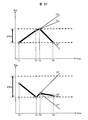
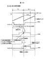
- FIG. 41 it is a figure which shows the example of a pulse waveform at the time of performing each process of step 941, 947, 948, and 949 in order.
- FIG. 42 is a diagram illustrating an example of a pulse waveform when the processes of steps 941, 947, and 948 are executed in order in the flowchart of FIG. 41 and the process of step 949 is not executed.
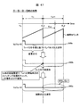
- FIG. 41 it is a figure which shows the example of a pulse waveform at the time of performing each process of step 941, 947, 948, and 949 in order.
- FIG. 42 is a diagram illustrating an example of a pulse waveform when the processes of steps 941, 947, and 948 are executed in order in the flowchart of FIG. 41 and the process of step 949 is not
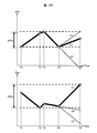
- FIG. 41 it is a figure which shows the example of a pulse waveform at the time of performing each process of step 941, 947, 950, and 951 in order.
- FIG. 41 it is a figure which shows the example of a pulse waveform when each process of step 941, 947, 950, and 952 is performed in order.
- the following embodiments can solve a desirable problem in commercialization and have a desirable effect in commercialization. Play. Some of them will be described next, and in the description of the embodiments, specific solutions to problems and specific effects will be described.
- a drive signal is switched from a drive circuit to control the switching operation of the switching element based on an AC magnetic flux ripple converted from DC power and a magnetic pole position signal of the motor. Supplying to the element, the switching element conducts or cuts off in association with the magnetic pole position of the motor.
- the number of switching operations of the switching element per unit time or the number of switching operations per cycle of AC power can be reduced as compared with a general PWM system.
- the switching frequency of the switching element of a power switching circuit is reduced, the loss of a motor can be suppressed and there exists an effect which can reduce the loss accompanying switching operation. This leads to a reduction in heat generation and demagnetization due to heat generation of the switching element of the power switching circuit and magnet eddy current of the motor.
- the fluctuation of the magnetic flux in the direction not having an interlinkage with the magnet or in a direction having few interlinking areas is allowed.
- the number of switching operations per unit time of the switching element of the power switching circuit can be reduced.
- the number of switching times of the switching element of the power switching circuit can be reduced.
- the switching element is preferably an element having a high operating speed and capable of controlling both conduction and cutoff operation based on a control signal.
- Examples of such an element include an insulated gate bipolar transistor (hereinafter referred to as IGBT) and a field effect transistor. (MOS transistor), and these elements are desirable in terms of responsiveness and controllability.
- the AC power output from the power converter is supplied to an inductance circuit composed of a rotating electrical machine and flows an AC current based on the action of the inductance.
- a rotating electrical machine that acts as a motor or a generator is described as an example of an inductance circuit.
- Use of the present invention to generate AC power for driving the rotating electrical machine is optimal from the viewpoint of effect, but it can also be used as a power conversion device that supplies AC power to an inductance circuit other than the rotating electrical machine.
- a power conversion device is a power conversion device that generates AC power for driving a rotating electrical machine of a hybrid vehicle (hereinafter referred to as HEV) or a pure electric vehicle (hereinafter referred to as EV).
- HEV hybrid vehicle
- EV pure electric vehicle
- HEV power converters and EV power converters are common in basic configuration and control, and as a representative example, a control configuration when the power converter according to the embodiment of the present invention is applied to a hybrid vehicle.
- the circuit configuration of the power converter will be described with reference to FIGS.
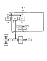
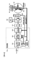
- FIG. 1 is a diagram showing a control block of a hybrid vehicle (hereinafter referred to as “HEV”).
- HEV hybrid vehicle
- Engine EGN and motor generator MG1 generate vehicle running torque.
- Motor generator MG1 not only generates rotational torque but also has a function of converting mechanical energy applied from the outside to motor generator MG1 into electric power.
- the motor generator MG1 is a synchronous machine and operates as a motor or a generator depending on the operation method as described above.
- motor generator MG1 When motor generator MG1 is mounted on an automobile, it is desirable to obtain a small size and high output, and a permanent magnet type synchronous motor using a magnet such as neodymium is suitable. Further, the permanent magnet type synchronous motor generates less heat from the rotor than the induction motor, and is excellent for automobiles from this viewpoint.
- the output torque on the output side of the engine EGN is transmitted to the motor generator MG1 via the power distribution mechanism TSM, and the rotation torque from the power distribution mechanism TSM or the rotation torque generated by the motor generator MG1 is transmitted via the transmission TM and the differential gear DEF. Transmitted to the wheels.
- rotational torque is transmitted from the wheels to motor generator MG1, and AC power is generated based on the supplied rotational torque.
- the generated AC power is converted to DC power by the power conversion device 200 as described later, and the high-voltage battery 136 is charged, and the charged power is used again as travel energy.
- the inverter circuit 140 is electrically connected to the battery 136 via the DC connector 138, and power is exchanged between the battery 136 and the inverter circuit 140.
- motor generator MG1 When motor generator MG1 is operated as a motor, inverter circuit 140 generates AC power based on DC power supplied from battery 136 via DC connector 138, and supplies it to motor generator MG1 via AC connector 188.
- the configuration comprising motor generator MG1 and inverter circuit 140 operates as a first motor generator unit.
- the vehicle can be driven only by the power of the motor generator MG1 by operating the first motor generator unit as an electric unit by the electric power of the battery 136. Further, in the present embodiment, the battery 136 can be charged by operating the first motor generator unit as a power generation unit by the power of the engine 120 or the power from the wheels to generate power.
- the battery 136 is also used as a power source for driving an auxiliary motor.
- the auxiliary motor is, for example, a motor for driving a compressor of an air conditioner or a motor for driving a control hydraulic pump.
- DC power is supplied from the battery 136 to the auxiliary power module, and the auxiliary power module generates AC power and supplies it to the auxiliary motor.
- the auxiliary power module has basically the same circuit configuration and function as the inverter circuit 140, and controls the phase, frequency, and power of alternating current supplied to the auxiliary motor.
- the power conversion device 200 includes a capacitor module 500 for smoothing the DC power supplied to the inverter circuit 140.
- the power conversion device 200 includes a communication connector 21 for receiving a command from a host control device or transmitting data representing a state to the host control device.
- Power conversion device 200 calculates a control amount of motor generator MG1 by control circuit 172 based on a command input from connector 21, further calculates whether to operate as a motor or a generator, and based on the calculation result.
- the control pulse is generated, and the control pulse is supplied to the driver circuit 174.
- the driver circuit 174 generates a driving pulse for controlling the inverter circuit 140 based on the supplied control pulse.
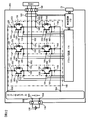
- FIG. 2 is a diagram illustrating a circuit configuration of the inverter circuit 140.
- an insulated gate bipolar transistor is used as a semiconductor element, and hereinafter abbreviated as IGBT.
- the IGBT 328 and the diode 156 that operate as the upper arm, and the IGBT 330 and the diode 166 that operate as the lower arm constitute the series circuit 150 of the upper and lower arms.
- the inverter circuit 140 includes the series circuit 150 corresponding to the three phases of the U phase, the V phase, and the W phase of the AC power to be output. That is, the inverter circuit 140 as a power switching circuit has a plurality of series circuits 150 in which an IGBT 328 that is an upper arm switching element and an IGBT 330 that is a lower arm switching element are connected in series.
- the series circuit 150 of the upper and lower arms of each of the three phases outputs an alternating current from a connection point (intermediate electrode) 169 that is a midpoint portion of the series circuit.
- the intermediate electrode 169 is connected to the motor generator MG1 through an AC bus bar 802 (described later) that connects the AC terminal 159 and the AC connector 188.
- the collector electrode 153 of the IGBT 328 of the upper arm is electrically connected to the capacitor terminal 506 on the positive electrode side of the capacitor module 500 via the positive electrode terminal 157.
- the emitter electrode of the IGBT 330 of the lower arm is electrically connected to the capacitor terminal 504 on the negative electrode side of the capacitor module 500 via the negative electrode terminal 158.
- control circuit 172 receives a control command from the host control device via the connector 21, and based on this, the IGBT 328 that configures the upper arm or the lower arm of each phase series circuit 150 that constitutes the inverter circuit 140. And a control pulse that is a control signal for controlling the IGBT 330 is generated and supplied to the driver circuit 174.
- the driver circuit 174 supplies a drive pulse for controlling the IGBT 328 and IGBT 330 constituting the upper arm or lower arm of each phase series circuit 150 to the IGBT 328 and IGBT 330 of each phase based on the control pulse.
- IGBT 328 and IGBT 330 perform conduction or cutoff operation based on the drive pulse from driver circuit 174, convert DC power supplied from battery 136 into three-phase AC power, and supply the converted power to motor generator MG1. Is done.
- the IGBT 328 includes a collector electrode 153, a signal emitter electrode 155, and a gate electrode 154.
- the IGBT 330 includes a collector electrode 163, a signal emitter electrode 165, and a gate electrode 164.
- a diode 156 is electrically connected between the collector electrode 153 and the emitter electrode 155.
- a diode 166 is electrically connected between the collector electrode 163 and the emitter electrode 165.
- MOSFET metal oxide semiconductor field effect transistor
- IGBT is suitable when the DC voltage is relatively high
- MOSFET is suitable when the DC voltage is relatively low.
- the capacitor module 500 includes a positive capacitor terminal 506, a negative capacitor terminal 504, a positive power terminal 509, and a negative power terminal 508.
- the high-voltage DC power from the battery 136 is supplied to the positive-side power terminal 509 and the negative-side power terminal 508 via the DC connector 138, and the positive-side capacitor terminal 506 and the negative-side capacitor of the capacitor module 500.
- the voltage is supplied from the terminal 504 to the inverter circuit 140.
- the DC power converted from the AC power by the inverter circuit 140 is supplied to the capacitor module 500 from the positive capacitor terminal 506 and the negative capacitor terminal 504, and is connected to the positive power terminal 509 and the negative power terminal 508. Is supplied to the battery 136 via the DC connector 138 and accumulated in the battery 136.
- the control circuit 172 includes a microcomputer (hereinafter referred to as “microcomputer”) for performing arithmetic processing on the switching timing of the IGBT 328 and the IGBT 330.
- the input information to the microcomputer includes a target torque value required for the motor generator MG1, a current value supplied from the series circuit 150 to the motor generator MG1, and a magnetic pole position of the rotor of the motor generator MG1.
- the target torque value is based on a command signal output from a host controller (not shown).
- the current value is detected based on a detection signal from the current sensor 180.
- the magnetic pole position is detected based on a detection signal output from a rotating magnetic pole sensor (not shown) such as a resolver provided in the motor generator MG1.
- the current sensor 180 detects the current value of three phases, but the current value for two phases may be detected and the current for three phases may be obtained by calculation. .
- the microcomputer in the control circuit 172 calculates the d and q axis current command values of the motor generator MG1 based on the inputted target torque value, and the calculated d and q axis current command values are detected. Based on the difference between the d and q axis current values, the d and q axis voltage command values are calculated, and a pulsed drive signal is generated from the d and q axis voltage command values.
- the control circuit 172 has a function of generating a drive signal of a method according to an embodiment of the present invention described later.
- the d-axis is a coordinate axis defined along the main magnetic flux direction by the permanent magnet arranged in the rotor of the motor generator MG1 which is a permanent magnet motor.
- the q-axis is a coordinate axis defined along a direction orthogonal to the d-axis (that is, the main magnetic flux).
- This method is a modulation method for controlling the switching operation of the IGBTs 328 and 330 which are switching elements based on the ripple of the AC waveform to be output and the magnetic pole position signal of the motor.
- the driver circuit 174 When driving the lower arm, the driver circuit 174 amplifies the pulse-like modulated wave signal and outputs it as a drive signal to the gate electrode of the corresponding lower arm IGBT 330.
- the reference potential level of the pulsed modulated wave signal When driving the upper arm, the reference potential level of the pulsed modulated wave signal is shifted to the reference potential level of the upper arm, and then the pulsed modulated wave signal is amplified and used as a drive signal. , Output to the gate electrode of the IGBT 328 of the corresponding upper arm. As a result, the IGBTs 328 and 330 perform a switching operation based on the input drive signal.
- the power conversion device 200 converts the voltage supplied from the battery 136, which is a DC power supply, to 2 ⁇ / in electrical angle.
- the output voltage is converted into U-phase, V-phase, and W-phase output voltages shifted every 3 rads, and supplied to a motor generator MG1 that is a three-phase AC motor.
- the electrical angle corresponds to the rotation state of motor generator MG1, specifically to the position of the rotor, and periodically changes between 0 and 2 ⁇ .
- the switching states of the IGBTs 328 and 330 that is, the output voltages of the U phase, the V phase, and the W phase can be determined according to the rotation state of the motor generator MG1.
- the microcomputer in the control circuit 172 detects abnormality (overcurrent, overvoltage, overtemperature, etc.) and protects the series circuit 150. For this reason, sensing information is input to the control circuit 172. For example, information on the current flowing through the emitter electrodes of the IGBTs 328 and IGBTs 330 is input to the corresponding drive units (ICs) from the signal emitter electrode 155 and the signal emitter electrode 165 of each arm. Thereby, each drive part (IC) detects overcurrent, and when overcurrent is detected, it stops the switching operation of corresponding IGBT328 and IGBT330, and protects corresponding IGBT328 and IGBT330 from overcurrent.
- ICs drive units
- Information on the temperature of the series circuit 150 is input to the microcomputer from a temperature sensor (not shown) provided in the series circuit 150.
- voltage information on the DC positive side of the series circuit 150 is input to the microcomputer.
- the microcomputer performs overtemperature detection and overvoltage detection based on such information, and stops switching operations of all the IGBTs 328 and IGBTs 330 when an overtemperature or overvoltage is detected.
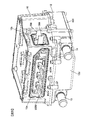
- FIG. 3 and 4 are external perspective views of the power conversion device 200 as an embodiment of the present invention.
- FIG. 4 shows a state where the AC connector 187 and the DC connector 138 are removed.
- the power conversion device 200 according to the present embodiment has an effect that the planar shape is a rectangular parallelepiped shape, which can be reduced in size and can be easily attached to the vehicle.
- 8 is a lid
- 10 is a housing
- 12 is a flow path forming body
- 13 is a cooling medium inlet pipe
- 14 is an outlet pipe
- 420 is a lower cover.
- the connector 21 is a signal connector provided for connection to the outside.
- the lid 8 is fixed to the upper opening of the housing 10 in which circuit components constituting the power conversion device 200 are accommodated.
- the flow path forming body 12 fixed to the lower part of the housing 10 holds a power module 300 and a capacitor module 500, which will be described later, and cools them with a cooling medium.
- a cooling medium For example, water is often used as the cooling medium, and will be described below as a refrigerant.
- the inlet pipe 13 and the outlet pipe 14 are provided on one side surface of the flow path forming body 12, and the refrigerant supplied from the inlet pipe 13 flows into a flow path 19 described later in the flow path forming body 12 and is discharged from the outlet pipe 14. Is done. Note that changing the inflow and outflow direction of the refrigerant does not significantly affect the cooling efficiency and pressure loss.
- the arrangement of the inlet pipe 13 and the outlet pipe 14 is symmetrical with respect to the central portion of the power conversion device 200. It has the advantage that it can be changed according to the situation.
- the AC interface 185 to which the AC connector 187 is attached and the DC interface 137 to which the DC connector 138 is attached are provided on the side surface of the housing 10.
- the AC interface 185 is provided on the side surface where the pipes 13 and 14 are provided, and the AC wiring 187 a of the AC connector 187 attached to the AC interface 185 extends downward between the pipes 13 and 14.
- the DC interface 137 is provided on the side surface adjacent to the side surface on which the AC interface 185 is provided, and the DC wiring 138 a of the DC connector 138 attached to the DC interface 137 also extends below the power converter 200.
- the AC interface 185 and the pipes 13 and 14 are arranged on the same side surface 12d side, and the AC wiring 187a is drawn downward so as to pass between the pipes 13 and 14, so the pipes 13, 14,
- the space occupied by the AC connector 187 and the AC wiring 187a can be reduced, and the overall size of the apparatus can be reduced. Further, since the AC wiring 187a is drawn downward with respect to the pipes 13 and 14, the AC wiring 187a can be easily routed and the productivity is improved.
- FIG. 5 is a diagram illustrating a state in which the lid 8, the DC interface 137, and the AC interface 185 are removed from the power conversion device 200 illustrated in FIG.
- An opening 10a to which the AC interface 185 is fixed is formed on one side of the housing 10, and an opening 10b to which the DC interface 137 is fixed is formed on the other adjacent side.
- Three AC bus bars 802, that is, a U-phase AC bus bar 802U, a V-phase AC bus bar 802V, and a W-phase AC bus bar 802W protrude from the opening 10a, and DC-side power supply terminals 508 and 509 protrude from the opening 10b.
- FIG. 6 is a view showing a state where the housing 10 is removed from the flow path forming body 12 in FIG.
- the housing 10 has two storage spaces, and is divided into an upper storage space and a lower storage space by a partition wall 10c.
- the control circuit board 20 to which the connector 21 is fixed is stored in the upper storage space, and the driver circuit board 22 and a bus bar assembly 800 described later are stored in the lower storage space.
- a control circuit 172 shown in FIG. 2 is mounted on the control circuit board 20, and a driver circuit 174 is mounted on the driver circuit board 22.
- the control circuit board 20 and the driver circuit board 22 are connected by a flat cable (not shown) (see FIG. 7 to be described later).
- the flat cable passes through a slit-shaped opening 10d formed in the partition wall 10c and is a lower storage space. To the upper storage space.
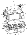
- FIG. 7 is an exploded perspective view of the power converter 200.
- the control circuit board 20 on which the control circuit 172 is mounted is disposed inside the lid 8, that is, in the upper storage space of the housing 10.
- An opening 8 a for the connector 21 is formed in the lid 8.
- Low voltage DC power for operating the control circuit in the power converter 200 is supplied from the connector 21.
- the flow path forming body 12 is formed with a flow path through which the refrigerant flowing from the inlet pipe 13 flows.
- the flow path forms a U-shaped flow path that flows along the three side surfaces of the flow path forming body 12.
- the refrigerant that has flowed from the inlet pipe 13 flows into the flow path from one end of the U-shaped flow path, flows through the flow path, and then flows out from the outlet pipe 14 connected to the other end of the flow path.
- Three openings 402a to 402c are formed on the upper surface of the flow path, and the power modules 300U, 300V, and 300W including the series circuit 150 (see FIG. 1) are inserted into the flow path from the openings 402a to 402c. Inserted.
- the power module 300U includes a U-phase series circuit 150
- the power module 300V includes a V-phase series circuit 150
- the power module 300W includes a W-phase series circuit 150.
- These power modules 300U to 300W have the same configuration and the same external shape.
- the openings 402a to 402c are closed by the flange portions of the inserted power modules 300U to 300W.
- a storage space 405 for storing electrical components is formed in the flow path forming body 12 so as to be surrounded by the U-shaped flow path.
- the capacitor module 500 is stored in the storage space 405.
- the capacitor module 500 stored in the storage space 405 is cooled by the refrigerant flowing in the flow path.
- a bus bar assembly 800 to which AC bus bars 802U to 802W are attached is disposed above the capacitor module 500.
- the bus bar assembly 800 is fixed to the upper surface of the flow path forming body 12.
- a current sensor 180 is fixed to the bus bar assembly 800.
- the driver circuit board 22 is disposed above the bus bar assembly 800 by being fixed to a support member 807a provided in the bus bar assembly 800. As described above, the control circuit board 20 and the driver circuit board 22 are connected by the flat cable 23. The flat cable 23 is pulled out from the lower storage space to the upper storage space through the slit-shaped opening 10d formed in the partition wall 10c.
- the power modules 300U to 300W, the driver circuit board 22 and the control circuit board 20 are hierarchically arranged in the height direction, and the control circuit board 20 is arranged at a place farthest from the high power system power modules 300U to 300W. Therefore, it is possible to reduce mixing of switching noise and the like on the control circuit board 20 side. Furthermore, since the driver circuit board 22 and the control circuit board 20 are arranged in different storage spaces partitioned by the partition wall 10c, the partition wall 10c functions as an electromagnetic shield and enters the control circuit board 20 from the driver circuit board 22. Noise can be reduced.
- the housing 10 is made of a metal material such as aluminum.
- control circuit board 20 is fixed to the partition wall 10c formed integrally with the housing 10, the mechanical resonance frequency of the control circuit board 20 is increased against external vibration. Therefore, it is difficult to be affected by vibration from the vehicle side, and reliability is improved.
- FIG. 8 is an external perspective view in which the power modules 300U to 300W, the capacitor module 500, and the bus bar assembly 800 are assembled to the flow path forming body 12.
- FIG. 9 shows a state in which the bus bar assembly 800 is removed from the flow path forming body 12.
- the bus bar assembly 800 is bolted to the flow path forming body 12.
- FIG. 10 is a perspective view of the flow path forming body 12
- FIG. 11 is an exploded perspective view of the flow path forming body 12 as seen from the back side.
- the flow path forming body 12 is a rectangular parallelepiped having a planar shape, and an inlet pipe 13 and an outlet pipe 14 are provided on a side surface 12d thereof.
- the side surface 12d is formed in a stepped portion in which the pipes 13 and 14 are provided.
- the channel 19 is formed in a U shape so as to follow the remaining three side surfaces 12a to 12c.
- a U-shaped opening 404 connected to one having the same shape as the cross-sectional shape of the flow path 19 is formed on the back surface side of the flow path forming body 12.
- the opening 404 is closed by a U-shaped lower cover 420.
- a seal member 409a is provided between the lower cover 420 and the flow path forming body 12, and airtightness is maintained.
- the U-shaped channel 19 is divided into three channel sections 19a, 19b, and 19c according to the direction in which the refrigerant flows.
- the first flow path section 19a is provided along the side face 12a at a position facing the side face 12d provided with the pipes 13 and 14, and the second flow path section 19b is one of the side faces 12a.
- the third flow path section 19c is provided along the side surface 12c adjacent to the other side of the side surface 12a.
- the refrigerant flows from the inlet pipe 13 into the flow path section 19b, flows in the order of the flow path section 19b, the flow path section 19a, and the flow path section 19c as shown by the broken line arrows, and flows out from the outlet pipe 14.
- a rectangular opening 402a parallel to the side surface 12a is formed at a position facing the flow path section 19a, and at a position facing the flow path section 19b.
- a rectangular opening 402b parallel to the side surface 12b is formed, and a rectangular opening 402c parallel to the side surface 12c is formed at a position facing the flow path section 19c.
- the power modules 300U to 300W are inserted into the flow path 19 through these openings 402a to 402c.
- the lower cover 420 is formed with a convex portion 406 protruding downward from the flow path 19 at a position facing the above-described openings 402a to 402c. These protrusions 406 are indented when viewed from the flow path 19 side, and the lower end portions of the power modules 300U to 300W inserted from the openings 402a to 402c enter these indentations. Since the flow path forming body 12 is formed so that the opening 404 and the openings 402a to 402c face each other, the flow path forming body 12 is configured to be easily manufactured by aluminum casting.
- the flow path forming body 12 is provided with a rectangular storage space 405 formed so that three sides are surrounded by the flow path 19.
- the capacitor module 500 is stored in the storage space 405. Since the storage space 405 surrounded by the flow path 19 has a rectangular parallelepiped shape, the capacitor module 500 can be formed into a rectangular parallelepiped shape, and the productivity of the capacitor module 500 is improved.
- the power modules 300U to 300W and the power modules 301a to 301c used in the inverter circuit 140 will be described.
- the power modules 300U to 300W and the power modules 301a to 301c all have the same structure, and the structure of the power module 300U will be described as a representative.
- the signal terminal 325U corresponds to the gate electrode 154 and the signal emitter electrode 155 disclosed in FIG. 2
- the signal terminal 325L corresponds to the gate electrode 164 and the emitter electrode 165 disclosed in FIG.
- the DC positive terminal 315B is the same as the positive terminal 157 disclosed in FIG. 2
- the DC negative terminal 319B is the same as the negative terminal 158 disclosed in FIG.
- the AC terminal 320B is the same as the AC terminal 159 disclosed in FIG.
- FIG. 12A is a perspective view of the power module 300U of the present embodiment.
- FIG. 12B is a cross-sectional view of the power module 300 ⁇ / b> U of the present embodiment cut along a cross section D and viewed from the direction E.
- FIGS. 13 (a), 13 (b), and 13 (c) show the screw 309 and the second sealing resin from the power module 300U shown in FIGS. 12 (a) and 12 (b) to facilitate understanding. It is a figure which shows the state which removed 351. 13 (a) is a perspective view, and FIG. 13 (b) is similar to FIG. 12 (b), and the power module 300U in the state shown in FIG. FIG. FIG. 13C is a cross-sectional view of the power module 300U before the fins 305 are pressed and the bending portion 304A is deformed.
- FIGS. 13 (a) and 14 (b) are views showing a state where the module case 304 is further removed from the power module 300U shown in FIGS. 13 (a) and 13 (b).
- 14A is a perspective view
- FIG. 14B is a cross-sectional view of the power module 300U in the state shown in FIG. 14A, similar to FIGS. 12B and 13B. Then, it is a sectional view when viewed from the direction E.
- FIG. 15 is a perspective view of the power module 300U in which the first sealing resin 348 and the wiring insulating portion 608 are further removed from the states shown in FIGS. 14 (a) and 14 (b).
- FIG. 16 is a diagram for explaining an assembly process of the module primary sealing body 302.
- the power semiconductor elements (IGBT 328, IGBT 330, diode 156, and diode 166) constituting the upper and lower arm series circuit 150 are replaced by the conductor plate 315, the conductor plate 318, or the conductor plate 320 as shown in FIGS. And are fixed by being sandwiched from both sides by a conductor plate 319.
- the conductor plate 315 and the like are sealed with the first sealing resin 348 with the heat dissipation surface exposed, and the insulating sheet 333 is thermocompression bonded to the heat dissipation surface.
- the first sealing resin 348 has a polyhedral shape (here, a substantially rectangular parallelepiped shape).
- the module primary sealing body 302 sealed with the first sealing resin 348 is inserted into the module case 304 and sandwiched with the insulating sheet 333, and is thermocompression bonded to the inner surface of the module case 304 that is a CAN type cooler.
- the CAN-type cooler is a cylindrical cooler having an insertion port 306 on one surface and a bottom on the other surface.
- the gap remaining inside the module case 304 is filled with the second sealing resin 351.
- the module case 304 is made of a member having electrical conductivity, for example, an aluminum alloy material (Al, AlSi, AlSiC, Al—C, etc.), and is integrally formed without a joint.
- the module case 304 has a structure in which no opening other than the insertion port 306 is provided, and the outer periphery of the insertion port 306 is surrounded by a flange portion 304B. Also, as shown in FIG. 12 (a), the first heat radiating surface 307A and the second heat radiating surface 307B, which are wider than the other surfaces, are arranged facing each other so as to face these heat radiating surfaces.
- Each power semiconductor element (IGBT 328, IGBT 330, diode 156, diode 166) is arranged.
- the three surfaces that connect the first heat radiation surface 307A and the second heat radiation surface 307B that face each other constitute a surface that is sealed with a narrower width than the first heat radiation surface 307A and the second heat radiation surface 307B, and the other one side surface
- An insertion port 306 is formed at the bottom.
- the shape of the module case 304 does not need to be an accurate rectangular parallelepiped, and the corner may form a curved surface as shown in FIG.
- the metal case having such a shape By using the metal case having such a shape, even when the module case 304 is inserted into the flow path 19 through which a coolant such as water or oil flows, a seal against the coolant can be secured by the flange portion 304B. It is possible to prevent the medium from entering the inside of the module case 304 with a simple configuration.
- the fins 305 are uniformly formed on the first heat radiation surface 307A and the second heat radiation surface 307B facing each other.
- a curved portion 304A having an extremely thin thickness is formed on the outer periphery of the first heat radiating surface 307A and the second heat radiating surface 307B. Since the curved portion 304A is extremely thin to such an extent that it can be easily deformed by pressurizing the fin 305, the productivity after the module primary sealing body 302 is inserted is improved.
- the gap between the conductor plate 315 and the inner wall of the module case 304 can be reduced by thermocompression bonding the conductor plate 315 and the like to the inner wall of the module case 304 via the insulating sheet 333, and the power semiconductor The generated heat of the element can be efficiently transmitted to the fin 305. Further, by providing the insulating sheet 333 with a certain degree of thickness and flexibility, the generation of thermal stress can be absorbed by the insulating sheet 333, which is favorable for use in a power conversion device for a vehicle having a large temperature change. .
- a metallic DC positive wiring 315A and a DC negative wiring 319A for electrical connection with the capacitor module 500 are provided, and a DC positive terminal 315B (157) and a DC are connected to the tip thereof. Negative terminals 319B (158) are formed respectively.
- metallic AC wiring 320A for supplying AC power to motor generator MG1 is provided, and AC terminal 320B (159) is formed at the tip thereof.
- the DC positive electrode wiring 315A is connected to the conductor plate 315
- the DC negative electrode wiring 319A is connected to the conductor plate 319
- the AC wiring 320A is connected to the conductor plate 320.
- metal signal wirings 324U and 324L for electrical connection with the driver circuit 174 are further provided, and signal terminals 325U (154, 155) and a signal terminal 325L are provided at the front ends thereof. (164: gate electrode, 165: emitter electrode) are formed.
- the signal wiring 324U is connected to the IGBT 328
- the signal wiring 324L is connected to the IGBT 328.
- the DC positive electrode wiring 315A, the DC negative electrode wiring 319A, the AC wiring 320A, the signal wiring 324U, and the signal wiring 324L are integrally molded as the auxiliary mold body 600 in a state where they are insulated from each other by the wiring insulating portion 608 formed of a resin material. Is done.
- the wiring insulating portion 608 also acts as a support member for supporting each wiring, and a thermosetting resin or a thermoplastic resin having an insulating property is suitable for the resin material used therefor. Thereby, it is possible to secure insulation between the DC positive electrode wiring 315A, the DC negative electrode wiring 319A, the AC wiring 320A, the signal wiring 324U, and the signal wiring 324L, and high-density wiring is possible.
- the auxiliary mold body 600 is fixed to the module case 304 with a screw 309 that passes through a screw hole provided in the wiring insulating portion 608 after being metal-bonded to the module primary sealing body 302 at the connection portion 370.
- TIG welding or the like can be used for metal bonding between the module primary sealing body 302 and the auxiliary mold body 600 in the connection portion 370.
- the direct current positive electrode wiring 315A and the direct current negative electrode wiring 319A are stacked on each other in a state of facing each other with the wiring insulating portion 608 interposed therebetween, and have a shape extending substantially in parallel. With such an arrangement and shape, the current that instantaneously flows during the switching operation of the power semiconductor element flows oppositely and in the opposite direction. As a result, the magnetic fields produced by the currents cancel each other out, and this action can reduce the inductance.
- the AC wiring 320A and the signal terminals 325U and 325L also extend in the same direction as the DC positive electrode wiring 315A and the DC negative electrode wiring 319A.
- connection portion 370 in which the module primary sealing body 302 and the auxiliary mold body 600 are connected by metal bonding is sealed in the module case 304 by the second sealing resin 351.
- the auxiliary module 600 side DC positive connection terminal 315C, the auxiliary module side DC negative connection terminal 319C, the auxiliary module side AC connection terminal 320C, and the auxiliary module side signal connection are connected to the auxiliary module 600 side of the connecting portion 370.
- Terminals 326U and auxiliary module side signal connection terminals 326L are arranged in a line.
- connection portion 370 On the other hand, on the module primary sealing body 302 side of the connection portion 370, along one surface of the first sealing resin 348 having a polyhedral shape, an element side DC positive connection terminal 315D, an element side DC negative connection terminal 319D, The element side AC connection terminal 320D, the element side signal connection terminal 327U, and the element side signal connection terminal 327L are arranged in a line.
- the structure in which the terminals are arranged in a row in the connection portion 370 facilitates the manufacture of the module primary sealing body 302 by transfer molding.
- a terminal constituted by the DC positive electrode wiring 315A (including the DC positive electrode terminal 315B and the auxiliary module side DC positive electrode connection terminal 315C) and the element side DC positive electrode connection terminal 315D is referred to as a positive electrode side terminal.
- a terminal composed of the DC negative electrode terminal 319B (including the auxiliary module side DC negative electrode connection terminal 319C) and the element side DC negative electrode connection terminal 315D is referred to as a negative electrode side terminal, and AC wiring 320A (AC terminal 320B and auxiliary module side AC connection)
- the terminal composed of the terminal 320C and the element side AC connection terminal 320D is referred to as an output terminal, and is composed of the signal wiring 324U (including the signal terminal 325U and the auxiliary module side signal connection terminal 326U) and the element side signal connection terminal 327U.
- Element side DC positive electrode connecting terminal 315D Element side DC negative connection terminal 319D, element side AC connection terminal 320D, element side signal connection terminal 327U and element side signal connection terminal 327L) are one surface of the first sealing resin 348 having a polyhedral shape as described above. Are lined up in a row. Further, the positive electrode side terminal and the negative electrode side terminal protrude in a stacked state from the second sealing resin 351 and extend outside the module case 304.
- the power semiconductor element and the terminal are connected during mold clamping when the module primary sealing body 302 is manufactured by sealing the power semiconductor element with the first sealing resin 348. It is possible to prevent an excessive stress on the portion and a gap in the mold from occurring. Further, since the magnetic fluxes in the directions canceling each other are generated by the currents in the opposite directions flowing through each of the stacked positive electrode side terminals and negative electrode side terminals, the inductance can be reduced.
- the auxiliary module side DC positive electrode connection terminal 315C and the auxiliary module side DC negative electrode connection terminal 319C are the DC positive electrode terminal 315B and the tip of the DC positive electrode wiring 315A and the DC negative electrode wiring 319A opposite to the DC negative electrode terminal 319B. It is formed in each part. Further, the auxiliary module side AC connection terminal 320C is formed at the tip of the AC wiring 320A opposite to the AC terminal 320B. The auxiliary module side signal connection terminals 326U and 326L are formed at the distal ends of the signal wirings 324U and 324L opposite to the signal terminals 325U and 325L, respectively.
- the element side DC positive connection terminal 315D, the element side DC negative connection terminal 319D, and the element side AC connection terminal 320D are formed on the conductor plates 315, 319, and 320, respectively.
- the element side signal connection terminals 327U and 327L are connected to the IGBTs 328 and 330 by bonding wires 371, respectively.
- FIG. 17 is an external perspective view of the capacitor module 500.
- a plurality of capacitor cells are provided in the capacitor module 500.
- Capacitor terminals 503a to 503c are provided on the upper surface of the capacitor module 500 so as to protrude close to the surface of the capacitor module 500 facing the flow path 19.
- the capacitor terminals 503a to 503c are formed corresponding to the positive terminal 157 and the negative terminal 158 of each power module 300.
- the capacitor terminals 503a to 503c have the same shape, and an insulating sheet is provided between the negative electrode side capacitor terminal 504 and the positive electrode side capacitor terminal 506 constituting the capacitor terminals 503a to 503c, and insulation between the terminals is ensured. Yes.
- Projections 500e and 500f are formed on the upper side of the side surface 500d of the capacitor module 500.
- a discharge resistor is mounted in the protruding portion 500e, and a Y capacitor for countering common mode noise is mounted in the protruding portion 500f.
- the power supply terminals 508 and 509 shown in FIG. 5 are attached to the terminals 500g and 500h protruding from the upper surface of the protruding portion 500f.
- recesses 405a and 405b are formed between the openings 402b and 402c and the side surface 12d.
- the discharge resistor mounted in the protruding portion 500e is a resistor for discharging the electric charge accumulated in the capacitor cell in the capacitor module 500 when the inverter is stopped. Since the recessed portion 405a in which the protruding portion 500e is accommodated is provided immediately above the flow path of the refrigerant flowing in from the inlet pipe 13, it is possible to suppress the temperature rise of the discharge resistance during discharge.
- FIG. 18 is a perspective view of the bus bar assembly 800.
- the bus bar assembly 800 detects U, V, W phase AC bus bars 802U, 802V, 802W, a holding member 803 for holding and fixing the AC bus bars 802U to 802W, and an AC current flowing through the AC bus bars 802U to 802W.
- AC bus bars 802U to 802W are each formed of a wide conductor.
- a plurality of support members 807 a for holding the driver circuit board 22 are formed on the holding member 803 made of an insulating material such as resin so as to protrude upward from the holding member 803.
- the current sensor 180 is parallel to the side face 12d at a position close to the side face 12d of the flow path forming body 12.
- the current sensor 180 Located in the assembly 800.
- through-holes 181 for penetrating the AC bus bars 802U to 802W are formed.
- a sensor element is provided in a portion where the through hole 181 of the current sensor 180 is formed, and a signal line 182 a of each sensor element protrudes from the upper surface of the current sensor 180.
- Each sensor element is arranged side by side in the extending direction of the current sensor 180, that is, in the extending direction of the side surface 12 d of the flow path forming body 12.
- the AC bus bars 802U to 802W pass through the respective through holes 181 and their tip portions protrude in parallel.
- the holding member 803 is formed with positioning projections 806a and 806b protruding upward.
- the current sensor 180 is fixed to the holding member 803 by screwing.
- the protrusions 806a and 806b are engaged with the positioning holes formed in the frame of the current sensor 180, thereby positioning the current sensor 180. Is done.
- the positioning projections 806a and 806b are engaged with the positioning holes formed on the driver circuit board 22 side, whereby the signal line 182a of the current sensor 180 is obtained. Is positioned in the through hole of the driver circuit board 22.
- the signal line 182a is joined to the wiring pattern of the driver circuit board 22 by solder.
- the holding member 803, the support member 807a, and the protrusions 806a and 806b are integrally formed of resin. As described above, since the holding member 803 has a function of positioning the current sensor 180 and the driver circuit board 22, assembly and solder connection work between the signal line 182a and the driver circuit board 22 are facilitated. Further, by providing the holding member 803 with a mechanism for holding the current sensor 180 and the driver circuit board 22, the number of components as the whole power conversion device can be reduced.
- the AC bus bars 802U to 802W are fixed to the holding member 803 so that the wide surfaces are horizontal, and the connection portion 805 connected to the AC terminals 159 of the power modules 300U to 300W rises vertically.
- the connecting portion 805 has a concavo-convex shape at the tip, and has a shape in which heat concentrates on the concavo-convex portion during welding.
- the AC bus bars 802U to 802W protruding from the through holes 181 of the current sensor 180 are connected to the side surface of the flow path forming body 12. 12d. Since the power modules 300U to 300W are arranged in the flow path sections 19a, 19b, and 19c formed along the side surfaces 12a, 12b, and 12c of the flow path forming body 12, the connection portions 805 of the AC bus bars 802U to 802W are The bus bar assembly 800 is disposed at a position corresponding to the side surfaces 12a to 12c. As a result, as shown in FIG.
- the U-phase AC bus bar 802U extends from the power module 300U disposed in the vicinity of the side surface 12b to the side surface 12d, and the V-phase AC bus bar 802V is disposed in the vicinity of the side surface 12a. Extending from module 300V to side surface 12d, W-phase AC bus bar 802W extends from power module 300W disposed near side surface 12c to side surface 12d.
- FIG. 19 is a diagram showing the flow path forming body 12 in which the power modules 300U to 300W are fixed to the openings 402a to 402c and the capacitor module 500 is stored in the storage space 405.
- the U-phase power module 300U is fixed to the opening 402b
- the V-phase power module 300V is fixed to the opening 402a
- the W-phase power module 300W is fixed to the opening 402c.
- the capacitor module 500 is stored in the storage space 405, and the terminals on the capacitor side and the terminals of each power module are connected by welding or the like. Each terminal protrudes from the upper end surface of the flow path forming body 12, and a welding operation is performed by approaching a welding machine from above.
- the DC positive terminals 315B and DC negative terminals 319B of the power modules 300U to 300W arranged in a U-shape are capacitor terminals 503a to 503c provided to protrude from the upper surface of the capacitor module 500 shown in FIG. Connected. Since the three power modules 300U to 300W are provided so as to surround the capacitor module 500, the positional relationship of the power modules 300U to 300W with respect to the capacitor module 500 is equivalent, and the capacitor terminals 503a to 503c having the same shape are used.
- the capacitor module 500 can be connected in a well-balanced manner. For this reason, the circuit constants of the capacitor module 500 and the power modules 300U to 300W are easily balanced in each of the three phases, and the current can be easily taken in and out.
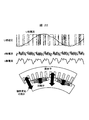
- FIG. 20 and 21 are conceptual diagrams of fluctuations of the U-phase voltage, the U-phase current, the d-axis current, the q-axis current, and the magnetic flux when the PWM control is applied.
- the PWM control is a method of controlling the switching element by determining the timing of conduction and interruption of the switching element based on the magnitude comparison between the carrier wave having a constant frequency and the AC waveform to be output. When PWM control is used, if the carrier frequency is set high as shown in FIG.
- the magnet eddy current loss is caused by slot harmonics caused by the slot shape of the motor and current harmonics contained in the current flowing through the windings of the motor stator.
- PWM control a change occurs in the eddy current loss of the magnet due to a difference in switching frequency. This is due to the difference in ripple behavior of current harmonics.
- the mechanism of the eddy current loss of the magnet is described with attention to current harmonics as follows. Magnetomotive force harmonics generated by current harmonics become harmonics of magnetic flux by the magnetic circuit of the motor and fluctuate the magnetic flux of the rotor.
- the rotor of the permanent magnet type synchronous motor is generally composed of a silicon steel plate and a neodymium magnet, and each member has conductivity.
- the method is limited to a method of reducing the entire magnetic flux harmonic.
- the modulation method according to the present invention can selectively reduce the fluctuation of the magnetic flux passing through the neodymium magnet without increasing the number of times the inverter is switched per unit time, and can reduce the eddy current loss of the rotor. .
- FIG. 22 is a conceptual diagram of fluctuations in the U-phase voltage, U-phase current, d-axis current, q-axis current, and magnetic flux when the modulation method according to the present invention is applied.
- the amount of change in the magnetic flux on the rotor can be arbitrarily controlled by controlling the ripples of the d-axis magnetic flux and the q-axis magnetic flux, respectively, by a method described later.
- This control by reducing the fluctuation of the magnetic flux passing through the neodymium magnet with respect to the fluctuation of the magnetic flux passing through the silicon steel sheet, the generation of eddy current in the neodymium magnet is suppressed, and the motor loss can be reduced.
- inverter loss is reduced by thinning out the number of times the inverter is switched.
- FIG. 23 shows each phase voltage pulse of UVW3 phase, d-axis current Id, q-axis current Iq, and each phase current of UVW3 phase when the modulation method according to the present invention is applied.
- the current ripple is controlled to fall within a predetermined range.
- each phase current of UVW is also substantially sinusoidal.
- each phase voltage pulse does not switch at a constant cycle as in PWM control, and there is no strict regularity in the switching interval. In other words, since the switching timing is determined based on the current ripple in this method, the loss of the motor is carefully managed and there is no possibility of unnecessary fine switching. Therefore, there is an effect of reducing the number of switching times.
- FIG. 24 is an example of a conceptual diagram showing a method for determining a desired output voltage vector for a predetermined voltage command in the modulation system according to the present invention.
- a command voltage vector, an output voltage vector, and a relative voltage vector between the output voltage vector and the command voltage vector are shown.
- the directions of the d axis and the q axis and the command voltage vector V * (Vd * , Vq * ) are in the illustrated positional relationship, the command voltage vector V * belongs to the region “1”.
- an inverter two-level inverter
- the command voltage vector V * belongs to the region “1”
- the voltage vectors V1, V2, V0, and V7 in the vicinity thereof are sequentially selected as output voltage vectors, so that these output voltage vectors Can be made to coincide with the command voltage vector V * .
- the average voltage can be matched with the command voltage vector V *.
- the fluctuation of the magnetic flux is large, and switching is performed to suppress the fluctuation. Since the number of times may increase, this selection is not performed in this embodiment.
- the magnetic flux is formed by time-integrating the output voltage vectors of V1, V2, V0, and V7 selected for the region “1”.
- Vd * and Vq * are constant and the rotational speed of the motor is also constant
- the target locus of magnetic flux by the voltage-time product of the command voltage vector V * is a circle with a constant radius.
- the locus of the magnetic flux formed by the time product of the output voltage vectors of V1, V2, V0, and V7 tries to follow the target locus of the magnetic flux by the command voltage vector V *, but cannot follow it completely. Change remains.
- the voltage causing the fluctuation of the magnetic flux is represented by the relative voltage vectors V1 ′, V2 ′, V0 ′, V7 ′ in FIG. 24, and these are represented by the output voltage vectors V1, V2, V0, V7 and the command voltage vector V * . It is defined as follows:
- V0 and V7 are both zero-sized vectors on the plane of FIG. Therefore, both V0 'and V7' are voltage vectors having the same magnitude and direction. Even if either V0 or V7 is selected as the output voltage, there is no difference in the locus of the magnetic flux, but there may be a difference in the number of switching of the inverter, so it is preferable to select the one with fewer switching times. .
- FIGS. 25 to 28 show a selection method of the output voltage vectors V1, V2, and V7 with respect to the command voltage vector V * of FIG. 24 and how the magnetic flux changes during the selection.
- FIG. 25 when the output voltage vector V1, V2 or V7 is output by the inverter from the initial state of the magnetic flux at time T1, the relative voltage vector V1 ′, V2 ′ or V7 ′ is applied to the motor accordingly. These relative voltage vectors change the magnetic flux in the illustrated direction. This change in magnetic flux is depicted in FIG. 24 based on the magnitude and direction of each relative voltage vector of V1 ′, V2 ′, and V7 ′.
- next switch state switching time T3 is determined by selecting the output voltage vector V1
- next switch state switching time T4 is determined by selecting the output voltage vector V2.
- next switch state switching time T5 is determined by selecting the output voltage vector V1.
- the output voltage vector with respect to the command voltage vector V *, the switch switching timing, and the locus of the d-axis magnetic flux ⁇ d and the q-axis magnetic flux ⁇ q generated accordingly can get.
- the locus of magnetic flux is simulated in the microcomputer by the method as described above, and the switching timing is calculated.
- the concept for outputting the calculation result from the microcomputer terminal is shown in FIG.
- the upper part of the figure shows the trajectories of the d-axis magnetic flux ⁇ d and the q-axis magnetic flux ⁇ q that are simulated in the microcomputer.
- the middle part of the figure is a voltage vector to be selected in order to obtain a trajectory of the upper d-axis magnetic flux ⁇ d and q-axis ⁇ q.
- the lower part of the figure shows the U, V, and W phase pulse generation process in the microcomputer.
- the sawtooth wave is the timer counter
- the dotted line is the register value
- the solid line is the switching state of the gate of the upper arm of each phase. Since the switching state of the lower arm is generated complementarily from the upper arm, the illustration is omitted here. In practice, the switching state of the lower arm should be determined in consideration of the dead time generation mechanism.
- the principle operation will be described.
- the voltage vector to be selected and the switching timing are determined. Since this voltage vector is uniquely associated with the switching pattern of the U, V, and W phases, the switch state of each phase that changes with time is determined.
- the timing for switching the switch state of each phase is determined as the timing at which the sawtooth time counter value matches the register value set according to the switching timing.
- the register value can be arbitrarily set in the microcomputer, but the switching timing that can be set in one sawtooth period is one.
- the switch state can be switched from ON to OFF at time T2 by appropriately setting the register value in the sawtooth period including time T2.
- An arbitrary pulse can be obtained by executing this process for each of the U, V, and W phases at an arbitrary timing. Details will be described later.
- the d-axis magnetic flux fluctuation range ⁇ d and the q-axis magnetic flux fluctuation range ⁇ q shown in FIGS. 25 to 28 are the electric resistance value of a permanent magnet (neodymium magnet) provided in the rotor of the motor to be controlled, It is preferable to determine each according to the relationship with the electric resistance value of the iron core of the rotor. Specifically, when the electrical resistance value of the permanent magnet provided in the rotor is smaller than the electrical resistance value of the rotor core, the d-axis magnetic flux fluctuation range ⁇ d is set smaller than the q-axis magnetic flux fluctuation range ⁇ q. To do.
- the d-axis magnetic flux fluctuation range ⁇ d is set larger than the q-axis magnetic flux fluctuation range ⁇ q. In this way, motor loss can be further reduced.
- FIG. 30 shows a motor control system by the control circuit 172 according to the embodiment of the present invention.
- a torque command T * as a target torque value is input to the control circuit 172 from a host control device.
- This torque command T * is input to the torque command / current command converter 210 in the control circuit 172.
- the angular velocity calculator 260 calculates the electrical angular velocity ⁇ re based on the magnetic pole position signal ⁇ re of the motor generator 192 (corresponding to the motor generator MG1 in FIGS. 1 and 2) detected by the rotating magnetic pole sensor 193.
- the torque command / current command converter 210 uses the torque-rotation speed map data stored in advance based on the input torque command T * and the electrical angular speed ⁇ re calculated by the angular speed calculator 260, A d-axis current command signal Id * and a q-axis current command signal Iq * are obtained.
- the d-axis current command signal Id * and the q-axis current command signal Iq * obtained by the torque command / current command converter 210 are output to the current controller (ACR) 220.
- phase current detection signals lu, lv, and lw of the motor generator 192 detected by the current sensor 180 are based on the magnetic pole position signal ⁇ re from the rotating magnetic pole sensor 193 by a three-phase two-phase converter (not shown) on the control circuit 172. , D-axis current signal Id and q-axis current signal Iq.
- the current controller (ACR) 220 is converted from the d-axis current command signal Id * and the q-axis current command signal Iq * output from the torque command / current command converter 210 and the phase current detection signals lu, lv, and lw.
- the d-axis voltage command signal Vd * and the q-axis voltage command signal Vq * are calculated based on the d-axis current command signal Id * and the q-axis current command signal Iq * .
- the d-axis voltage command signal Vd * and the q-axis voltage command signal Vq * are determined so that the current flowing through the motor generator 192 follows the d-axis current command signal Id * and the q-axis current command signal Iq *.
- the d-axis voltage command signal Vd * and the q-axis voltage command signal Vq * obtained by the current controller (ACR) 220 are output to the pulse modulator 230.
- the pulse modulator 230 Based on the d-axis voltage command signal Vd * and the q-axis voltage command signal Vq * from the current controller 220 and the magnetic pole position signal ⁇ re from the rotating magnetic pole sensor 193, the pulse modulator 230 performs the U phase, V phase, Six types of pulse signals respectively corresponding to the upper and lower arms of the W phase are generated. Then, the generated pulse signal is output to the driver circuit 174. Based on this pulse signal, a drive signal is output from the driver circuit 174 to each switching element of the inverter circuit 140.
- a pulse signal is output as a modulated wave from the control circuit 172 to the driver circuit 174.
- the driver circuit 174 outputs a drive signal for conducting or blocking them to each switching element of the inverter circuit 140, that is, the upper arm IGBT 328 and the lower arm IGBT 330.
- the configuration of the pulse modulator 230 is shown in FIG.
- the pulse modulator 230 includes an ⁇ converter 231, a voltage vector region searcher 232, an SW state predictor 233, a three-phase SW time calculator 234, a pulse corrector 235, and a time counter comparator 236.
- the d-axis voltage command signal Vd * and the q-axis voltage command signal Vq * output from the current controller 220 are input to the ⁇ converter 231 and the SW state predictor 233 in the pulse modulator 230.
- FIG. 32 is a flowchart showing a procedure of pulse generation performed by the pulse modulator 230. Using each configuration shown in FIG. 31, the pulse modulator 230 executes each processing step of the flowchart shown in FIG. 32 for each predetermined control period, and generates a pulse.
- step 890 ⁇ conversion processing using the ⁇ converter 231 is performed.
- the ⁇ converter 231 converts the voltage command signal of the dq axis rotation coordinate system represented by the d axis voltage command signal Vd * and the q axis voltage command signal Vq * into the magnetic pole position signal of the rotating magnetic pole sensor 193.
- the voltage is converted into a voltage command signal of an ⁇ axis stationary coordinate system expressed by an ⁇ axis voltage command signal V ⁇ * and a ⁇ axis voltage command signal V ⁇ * . This conversion is expressed by equation (2).
- a voltage vector area search process using the voltage vector area search unit 232 is performed.
- the voltage vector region search unit 232 searches for a voltage vector region based on the ⁇ -axis voltage command signal V ⁇ * and the ⁇ -axis voltage command signal V ⁇ * from the ⁇ converter 231.
- the concept of the voltage vector area search process performed by the voltage vector area search unit 232 will be described with reference to the vector diagram of FIG.
- the ⁇ -axis voltage command signal V ⁇ * and the ⁇ -axis voltage command signal V ⁇ * from the ⁇ converter 231 can be drawn as one vector on the ⁇ plane.
- the ⁇ plane is divided into six regions “1” to “6” divided every 60 ° as shown in FIG.
- the vector on the ⁇ plane corresponding to the ⁇ -axis voltage command signal V ⁇ * and the ⁇ -axis voltage command signal V ⁇ * belongs to one of these regions.
- the voltage vector area search unit 232 searches this area and outputs voltage vector information corresponding to the searched area to the SW state predictor 233 described later.
- FIG. 34 is a flowchart showing the flow of the voltage vector region search process described above.
- the voltage vector area search unit 232 performs an arctangent calculation of the ⁇ -axis voltage command signal V ⁇ * and the ⁇ -axis voltage command signal V ⁇ * .
- the angle ⁇ v formed by the ⁇ -axis with respect to the voltage vector generated by the ⁇ -axis voltage command signal V ⁇ * and the ⁇ -axis voltage command signal V ⁇ * on the ⁇ plane is obtained by Expression (3).
- step 902 the voltage vector region searcher 232 performs processing for determining which angle range of the six regions “1” to “6” in FIG. 33 the deviation angle ⁇ v obtained in step 901 belongs to.
- the voltage vector area searcher 232 executes any one of steps 903a to 903f, and specifies any one of the areas “1” to “6” as a voltage vector area.
- the voltage vector area search unit 232 determines an output voltage vector corresponding to the voltage vector area specified in any of steps 903a to 903f.
- the two voltage vectors closest to the specified voltage vector region are determined as output voltage vectors.
- the region “1” is obtained as the voltage vector region in step 903a, according to FIG. 33, the region “1” is divided into the voltage vector V1 (1, 0, 0) and the voltage vector V2 (1, 1, 0). Therefore, the voltage vectors V1 and V2 are determined as output voltage vectors.
- regions “2” to “6” are obtained as voltage vector regions in steps 903b to 903f, two voltage vectors corresponding to each region are determined as output voltage vectors.
- step 905 the voltage vector region searcher 232 outputs voltage vector information representing the output voltage vector determined in step 904 to the SW state predictor 233.
- step 905 the voltage vector region search process by the voltage vector region search unit 232 is terminated, and the process proceeds to step 910 in FIG.
- step S910 SW state prediction processing using the SW state predictor 233 is performed.
- the SW state predictor 233 includes the voltage vector information output from the voltage vector area search unit 232 in the voltage vector area search process in step 900 and the d-axis voltage command input from the current controller 220.
- the trajectory of the d-axis magnetic flux ⁇ d and the trajectory of the q-axis magnetic flux ⁇ q are predicted for each control period. The switching state and switching time are determined from the prediction result.
- the switching state indicates whether the voltage level of each arm of the U, V, and W3 phases is high or low, and the switching time indicates the time from the beginning of the corresponding control cycle until the next switch switching occurs.
- the output voltage vector simulating the locus of the magnetic flux and the switching time are calculated according to the method described with reference to FIGS. From this calculation result, the SW state predictor 233 predicts the switching state and switching time in the next control cycle, and outputs the SW state information and SW time information.
- FIG. 35 (a) is a flowchart showing the flow of the SW state prediction process performed by the SW state predictor 233.
- the SW state predictor 233 acquires the locus of magnetic flux obtained by the process up to the previous time.
- the SW state predictor 233 specifies the magnetic flux at the start of the next control cycle based on the magnetic flux trajectory obtained in step 911 up to the previous time.
- the magnitude of the magnetic flux at the start of the next control cycle is specified from the respective magnetic flux trajectories.
- the SW state predictor 233 calculates a relative voltage vector based on the voltage vector information from the voltage vector region searcher 232 and the d-axis voltage command signal Vd * and the q-axis voltage command signal Vq *. .
- the SW state predictor 233 selects any one of the three relative voltage vectors calculated in step 913.
- a relative voltage vector is selected such that the time required to enter the ⁇ d and q-axis magnetic flux fluctuation range ⁇ q is the longest.
- the trajectory when the trajectory is extended in the direction corresponding to each relative voltage vector from the respective starting points, the trajectory becomes the d-axis magnetic flux fluctuation range ⁇ d or the q-axis magnetic flux fluctuation range ⁇ q.
- One relative voltage vector at which the position intersecting with the upper limit or lower limit of each is the latest time side is selected.
- the SW state predictor 233 determines the next switch switching time according to the relative voltage vector selected in step 914.
- the locus of the d-axis magnetic flux ⁇ d is extended in the direction corresponding to the relative voltage vector selected from the starting point
- the time when the locus intersects the upper limit or lower limit of the d-axis magnetic flux fluctuation range ⁇ d and the q-axis magnetic flux
- the trajectory of ⁇ q is extended in the direction corresponding to the relative voltage vector selected from the starting point
- the earlier of the time when the trajectory intersects the upper limit or lower limit of the q-axis magnetic flux fluctuation range ⁇ q whichever is earlier Determined as switch switching time.
- step 916 the SW state predictor 233 determines whether or not the next switch switching time determined in step 915 is within the next control cycle. If it is within the next control cycle, the process returns to step 914, and the above-described processes of steps 914 and 915 are repeated once starting from the magnetic flux at the next switch switching time. On the other hand, if the next switch switching time is after the next control cycle, the process proceeds to step 917.
- step 917 the SW state predictor 233 performs a zero vector selection process.
- the zero vector is selected in step 914, either the output voltage vector V0 or V7, which is the zero vector, is selected.
- V0 or V7 which is the zero vector
- the SW state predictor 233 performs a three-phase SW-like conversion process for converting the relative voltage vector selected in Step 914 into a three-phase SW state.
- FIG. 36 is a flowchart showing the flow of the three-phase SW-like conversion process.
- step 971 the SW state predictor 233 determines whether the output voltage vector corresponding to the relative voltage vector selected in step 914 is V0 to V7. Depending on the determination result, the SW state predictor 233 executes any one of steps 972a to 972h to determine the states of the U, V, and W phases according to the output voltage vector. That is, it is determined whether each of the U, V, and W phases is in a high state or a low state.
- step 973 the SW state predictor 233 outputs a calculation result indicating the states of the U, V, and W phases determined in any of steps 972a to 972h.
- the calculation result is output by substituting information indicating the determined states of the U, V, and W phases into a RAM (not shown).
- step 973 the SW state predictor 233 ends the process of step 970 in FIG. 35A and proceeds to step 918.
- step 918 the SW state predictor 233 is based on the states of the U, V, and W phases determined by the three-phase SW-like conversion processing in step 970 and the next switch switching time determined in step 915.
- the SW state information and SW time information are output to the three-phase SW time calculator 234. That is, SW state information indicating the states of the U, V, and W phases in the next control cycle and SW time information indicating the next switch switching time are output as a result of the SW state prediction process.
- steps 930 to 933 processing using the three-phase SW time calculator 234 is performed.
- the three-phase SW time calculator 234 receives the SW state information and SW time information output from the SW state predictor 233, and rises of the U, V, and W phase switches within the next control cycle. Calculate time and fall time.
- step 930 the three-phase SW time calculator 234 determines that the next switch switching time determined by the SW state prediction process in step 910 is within the next control cycle based on the SW time output from the SW state predictor 233. To determine whether it exists. If the next switch switching time exists within the next control cycle, the process proceeds to step 931; otherwise, the process proceeds to step 933.
- step 931 the three-phase SW time calculator 234 determines whether or not there is a possibility of further switching in the remaining period in the next control cycle. If there is a possibility, the process returns to Step 890, and if there is no possibility, the process proceeds to Step 932. This is determined by whether one of the rise time register and the fall time register of the subsequent time counter is free. As described above, each of the rising and falling register values can be set once within one control cycle.
- the three-phase SW time calculator 234 sets U, V, and W three-phase switching times.
- the rise time and fall time in each phase of UVW are calculated based on the SW state information and SW time information from the SW state predictor 233, and the rise and fall register values are calculated according to the calculation results. Set each. If the switch is not switched, the switching time stored in the register can be prevented from crossing the time counter by setting a time longer than the control period as the switching time.
- step 933 the three-phase SW time calculator 234 sets the switching time so as not to switch the U, V, and W3 phases during the next control cycle.
- the rise time and fall time of each UVW phase are set in the same manner as in step 932, but since the switches are not switched during the control cycle, all values larger than the control cycle are set as the switching time.
- the rising time Ton and the falling time Toff are set for the U, V, and W3 phases, respectively.
- Information on the rise time Ton and the fall time Toff is output from the three-phase SW time calculator 234 to the pulse corrector 235.
- a pulse correction process using the pulse corrector 235 is performed.
- the pulse corrector 235 is a part that realizes a function that is necessary because there are some prohibitions when the signal output from the three-phase SW time calculator 234 is inserted into the time counter comparator 236 at the subsequent stage. .
- the pulse corrector 235 performs the minimum pulse width limitation and the pulse continuity compensation on the rising time Ton and the falling time Toff output from the three-phase SW time calculator 234 in step 932 or 933.
- the pulse correction process is performed. The result is output to the time counter comparator 236 as the rising time Ton ′ and the falling time Toff ′ after pulse correction. The specific content of this pulse correction process will be described in detail later.
- steps 960 to 962 processing using the time counter comparator 236 is performed.
- the time counter comparator 236 applies the U-phase, V-phase, and W-phase upper and lower arms to the upper and lower arms based on the rise time Ton ′ and the fall time Toff ′ after pulse correction output from the pulse corrector 235.
- a pulse signal is generated as a switching command.
- the six kinds of pulse signals generated by the time counter comparator 236 for the upper and lower arms of each phase are output to the driver circuit 174 as described above. As a result, a drive signal is output from the driver circuit 174 to each switching element.
- step 960 the time counter comparator 236 uses the pulse correction rising time Ton ′ and falling time Toff ′ output from the pulse corrector 438 in step 940 at the start timing of the next control cycle Tn + 1.
- the target time value in the control cycle Tn + 1 is set and the target time value is updated.
- step 961 the time counter comparator 236 compares the value of the time counter with the target time value set in step 960. Based on the comparison result, the pulse signal is generated at the rising time Ton ′ after the pulse correction, and the pulse signal is generated at the falling time Toff ′ after the pulse correction, thereby generating the pulse signal.
- step 962 the time counter comparator 236 outputs the pulse signal generated in step 961 to the driver circuit 174.
- a pulse signal in which the fluctuation of the magnetic flux is limited within a predetermined range is generated while the number of switching is reduced as compared with the conventional PWM control.
- a pulse signal is output as a modulated wave from the control circuit 172 to the driver circuit 174.
- a drive signal is output from the driver circuit 174 to the IGBTs 328 and 330 of the inverter circuit 140.
- a control cycle of about several hundred ⁇ s is determined in advance as a control cycle for the motor generator 192 in response to a request from the system performance.
- the pulse modulator 230 repeatedly calculates the states of the IGBTs 328 and 330 serving as switching elements for each control period. Depending on the calculation result, a pulse signal in the next control cycle is generated and output to the driver circuit 174.
- FIG. 35B is a flowchart showing the flow of the SW state prediction process by another processing method executed in the SW state predictor 233.
- the SW state predictor 233 determines whether or not the voltage vector of the next processing cycle is fixed. If the voltage vector of the next processing cycle is fixed, the process proceeds to step 912A. In this case, ⁇ T of the current locus calculated in the previous cycle is longer than the PWM cycle, and recalculation is performed for the current locus of the portion carried over to the next cycle as a remainder.
- step 911A determines whether the voltage vector of the next processing cycle has been determined. If it is determined in step 911A that the voltage vector of the next processing cycle has not been determined, the process proceeds to step 916A. In this case, the movement time of the current locus in the hysteresis region for each obtained vector is obtained, and the vector that maximizes this time is selected.
- the time to each intersection between the current locus and the dq axis of the hysteresis region is obtained, and the smaller value is set as the movement time of the current locus of the vector. From the current trajectory candidates obtained for each vector, the one that takes the maximum time to cross the hysteresis region is obtained.
- steps 914A and 919A dq axis components Kd and Kq of each vector are obtained.
- the calculation formulas at this time are as shown in the figure.
- step 970 the SW state predictor 233 performs a three-phase SW conversion process according to the flowchart shown in FIG. That is, ON / OFF information for each phase of U, V, and W is set based on the obtained mode information of the output voltage vector. Since the ON / OFF state of each phase is uniquely determined by the output voltage vector, it can be determined by determining the mode information.
- FIG. 37 shows the basic principle of pulse generation by the pulse modulator 230 in this embodiment.
- the rising time Ton and the falling time Toff are calculated at the head of the control cycle Tn.
- the rising time Ton ′ and the falling time Toff ′ after pulse correction are determined, and the U-phase, V-phase, W-phase are used using the compare match function with the time counter.
- a pulse signal is output for each phase.
- FIG. 37 illustrates only the U-phase pulse signal, but the same applies to the V-phase and the W-phase.
- the pulse correction process is executed by the pulse corrector 235 in order to apply the minimum pulse width limitation and the pulse continuity compensation to the generated pulse.
- the minimum pulse width restriction means that when the pulse width corresponding to the rise time Ton and the fall time Toff calculated in step 932 or 933 is less than a predetermined minimum pulse width, the pulse width is set as the minimum pulse width. Is to output. The minimum pulse width at this time is determined according to the response speed of the IGBTs 328 and 330 which are switching elements.
- the pulse pattern changes between the pulse waveform generated based on the prediction one control cycle before and the pulse waveform to be generated in the current control cycle. In such a case, the pulse waveform is changed and output so that the pulse continuity is maintained.
- Such a change in the pulse pattern occurs when the state of the motor generator 192 changes suddenly due to a disturbance or the like, or when the control mode is switched.
- FIG. 38 shows an example of a pulse waveform output when pulse continuity compensation is not performed.
- the rise time Ton is calculated in the control cycle Tn ⁇ 1 by the method described above, and the pulse waveform 981a in the control cycle Tn is output.
- This pulse waveform 981a cannot be changed in the control cycle Tn.
- the pulse pattern changes in the control cycle Tn, and the pulse waveform 11b in the next control cycle Tn + 1 is calculated.
- the pulse waveform 981b is always off during the period of the control cycle Tn + 1 and there is no pulse, the rise time Ton and the fall time Toff are not set in the control cycle Tn + 1.
- the pulse waveform 981a already output in the control cycle Tn is on rather than off at time Tv1. Therefore, in the actual output pulse waveform 981c, the place that should be originally turned off in the control cycle Tn + 1 is turned on.
- pulse continuity compensation is not performed, pulse continuity may not be maintained when the pulse pattern changes midway.
- FIG. 39 shows an example of a pulse waveform output when pulse continuity compensation is performed.
- the pulse waveform 982b of the next control cycle Tn + 1 is calculated in the control cycle Tn
- the on / off state at the start time Tv1 of the pulse waveform 12b that is, the control state of conduction or cutoff of the IGBTs 328 and 330 as switching elements is confirmed.
- the pulse waveform 982a of the control cycle Tn is Compared with the pulse waveform 982a of the control cycle Tn.
- the corrected pulse waveform 982c is forcibly turned off at time Tv1.
- the time Tv1 is newly set as the fall time Toff ′ after pulse correction.
- the corrected pulse waveform 982c is forcibly turned on at time Tv1.
- the time Tv1 is newly set as the rise time Ton ′ after the pulse correction. Note that when the on / off state of the pulse waveform 982a and the pulse waveform 982b coincide at the time Tv1 and both pulse waveforms are continuous, such pulse continuity compensation is not performed.
- FIG. 40 shows an example of a pulse waveform output when the minimum pulse width restriction is performed.
- the minimum pulse width is limited and the pulse width is expanded to the minimum pulse width.
- a corrected pulse waveform 983d that is turned off at a timing shifted from the time Tv1 is output.
- a time corresponding to the pulse width after enlargement is newly set as the fall time Toff ′ after pulse correction.
- FIG. 40 shows an example in which the corrected pulse waveform is forcibly turned off, the same applies to the case where the pulse waveform is forcibly turned on.
- FIG. 41 shows a flowchart illustrating in detail the procedure of the pulse correction processing described above.
- the pulse corrector 235 determines whether or not the rise time Ton calculated by the three-phase SW time calculator 234 in step 932 or 933 in FIG. 32 exists during the next control cycle Tn + 1. If there is a rise time Ton during the control cycle Tn + 1, the process proceeds to step 942, and if not, the process proceeds to step 947.
- step 942 the pulse corrector 235 determines whether or not the fall time Toff calculated by the three-phase SW time calculator 234 in step 932 or 933 in FIG. 32 exists during the next control cycle Tn + 1. . If there is a fall time Toff during the control cycle Tn + 1, the process proceeds to step 943, and if not, the process proceeds to step 945.
- the pulse corrector 235 determines that the pulse width ⁇ T corresponding to the period from the rise time Ton to the fall time Toff, or the period from the fall time Toff to the rise time Ton is less than the predetermined minimum pulse width. It is determined whether or not.
- the pulse width ⁇ T can be obtained as a time difference between the rising time Ton and the falling time Toff. Further, the minimum pulse width can be determined in advance according to the response speed of the IGBTs 328 and 330 which are switching elements as described above. If the pulse width ⁇ T is less than the minimum pulse width, the process proceeds to step 944, and if it is greater than or equal to the minimum pulse width, the process proceeds to step 956.
- step 944 the pulse corrector 235 deletes the pulse calculated by the three-phase SW time calculator 234. That is, regardless of the values of the rising time Ton and the falling time Toff output from the three-phase SW time calculator 234, both the rising time Ton ′ and the falling time Toff ′ after the pulse correction are used as the time counter comparator 236. Do not output to. Thereby, the pulse signal generated by the time counter comparator 236 in step 962 of FIG. 32 does not change within the period of the control cycle Tn + 1, and the control state of conduction or cutoff of the IGBTs 328 and 330 as the switching elements is maintained. Like that. When step 944 is executed, the process proceeds to step 956.
- step 945 the pulse corrector 235 determines whether or not the head of the next control cycle Tn + 1 is an off region. If it is in the off region, that is, if the pulse waveform calculated by the three-phase SW time calculator 234 in the control cycle Tn is in the off state at time Tv1, the process proceeds to step 946. On the other hand, if it is in the ON region, that is, if the pulse waveform calculated by the three-phase SW time calculator 234 in the control cycle Tn is in the ON state at time Tv1, the process proceeds to step 953.
- step 946 the pulse corrector 235 forcibly lowers the pulse calculated by the three-phase SW time calculator 234 at the head of the next control cycle Tn + 1. That is, by newly setting the time Tv1 as the fall time Toff ′ after pulse correction, the pulse signal generated by the time counter comparator 236 in step 962 in FIG. 32 is forcibly turned off at the beginning of the control cycle Tn + 1. To be.
- step 946 when the relationship between the cutoff state of the IGBTs 328 and 330 in the control cycle Tn and the cutoff state of the IGBTs 328 and 330 in the next control cycle Tn + 1 is a discontinuous relationship, the IGBTs 328 and 330 This is done by adding the control of shutting down.
- step 946 the process proceeds to step 953.
- step 947 the pulse corrector 235 determines whether or not the fall time Toff calculated by the three-phase SW time calculator 234 in step 932 or 933 in FIG. 32 exists during the next control cycle Tn + 1. . If there is a fall time Toff during the control cycle Tn + 1, the process proceeds to step 948, and if not, the process proceeds to step 950.
- step 948 the pulse corrector 235 determines whether or not the head of the next control cycle Tn + 1 is the ON region. If it is in the ON region, that is, if the pulse waveform calculated by the three-phase SW time calculator 234 in the control cycle Tn is in the ON state at time Tv1, the process proceeds to step 949. On the other hand, if it is in the off region, that is, if the pulse waveform calculated by the three-phase SW time calculator 234 in the control cycle Tn is in the off state at time Tv1, the process proceeds to step 953.
- step 949 the pulse corrector 235 forcibly raises the pulse calculated by the three-phase SW time calculator 234 at the beginning of the next control cycle Tn + 1. That is, by newly setting the time Tv1 as the rising time Ton ′ after pulse correction, the pulse signal generated by the time counter comparator 236 is forcibly turned on at the beginning of the control cycle Tn + 1 in Step 962 of FIG. So that Thereby, in the pulse corrector 235, when the relationship between the conduction state of the IGBTs 328 and 330 in the control cycle Tn and the conduction state of the IGBTs 328 and 330 in the next control cycle Tn + 1 is a discontinuous relationship, the IGBTs 328 and 330 This is done by adding continuity control.
- step 949 is executed, the process proceeds to step 953.
- Step 950 the pulse corrector 235 determines whether or not the head of the next control cycle Tn + 1 is the ON region. If it is in the ON region, that is, if the pulse waveform calculated by the three-phase SW time calculator 234 in the control period Tn is in the ON state at time Tv1, the process proceeds to step 951. On the other hand, if it is in the off region, that is, if the pulse waveform calculated by the three-phase SW time calculator 234 in the control period Tn is in the off state at time Tv1, the process proceeds to step 952.
- step 951 as in step 949, the pulse corrector 235 forcibly raises the pulse calculated by the three-phase SW time calculator 234 at the beginning of the next control cycle Tn + 1. That is, by newly setting the time Tv1 as the rising time Ton ′ after pulse correction, the pulse signal generated by the time counter comparator 236 is forcibly turned on at the beginning of the control cycle Tn + 1 in Step 962 of FIG. So that Thereby, in the pulse corrector 235, when the relationship between the conduction state of the IGBTs 328 and 330 in the control cycle Tn and the conduction state of the IGBTs 328 and 330 in the next control cycle Tn + 1 is a discontinuous relationship, the IGBTs 328 and 330 This is done by adding continuity control.
- step 951 is executed, the process proceeds to step 953.
- step 952 similarly to step 946, the pulse corrector 235 forcibly lowers the pulse calculated by the three-phase SW time calculator 234 at the beginning of the next control cycle Tn + 1. That is, by newly setting the time Tv1 as the fall time Toff ′ after pulse correction, the pulse signal generated by the time counter comparator 236 in step 962 in FIG. 32 is forcibly turned off at the beginning of the control cycle Tn + 1. To be.
- step 952 when the relationship between the cutoff state of the IGBTs 328 and 330 in the control cycle Tn and the cutoff state of the IGBTs 328 and 330 in the next control cycle Tn + 1 is a discontinuous relationship, the IGBTs 328 and 330 This is done by adding the control of shutting down.
- step 952 the process proceeds to step 953.
- the pulse corrector 235 obtains the information on the rising time Ton ′ or the falling time Toff ′ after the pulse correction calculated in the previous control cycle Tn ⁇ 1 as the previous value, and based on this previous value.
- Calculate the pulse width at forced switching That is, the time Tv1 newly set as the rising time Ton ′ or the falling time Toff ′ after the current pulse correction in the steps 946, 949, 951 or 952, and the rising time Ton ′ or the falling time Toff ′ of the previous value.
- the information of the rise time Ton ′ or the fall time Toff ′ of the previous value is acquired in step 956 described later. When a plurality of phase values are stored as the previous rise time Ton ′ or fall time Toff ′, the one closest to the time Tv1 is acquired.
- Step 954 the pulse corrector 235 determines whether or not the pulse width at the time of forced switching calculated in Step 953 is less than the minimum pulse width. The same minimum pulse width as that used in the determination of step 943 is used. If the pulse width at the time of forced switching is less than the minimum pulse width, the process proceeds to step 955, and if it is greater than the minimum pulse width, the process proceeds to step 956.
- step 955 the pulse corrector 235 sets the pulse width at the time of forced switching calculated in step 953 to be the minimum pulse width. That is, the value of the rising time Ton ′ or the falling time Toff ′ after the current pulse correction set in the steps 946, 949, 951 or 952 is changed from the initial setting value ⁇ v1, and the rising of the previous value It is assumed that a time value corresponding to the minimum pulse width is added to the time Ton ′ or the fall time Toff ′. Thereby, the pulse corrector 235 limits the pulse width at the time of forced switching so as not to be less than the minimum pulse width.
- steps 946, 949, 951, and 952 are executed, the processes of steps 953 to 955 may be omitted.
- step 956 the pulse corrector 235 outputs the rising time Ton ′ or the falling time Toff ′ after the pulse correction finally determined by the above processes to the time counter comparator 236. That is, if it is determined in step 943 that the pulse width ⁇ T is equal to or greater than the minimum pulse width, the rise time Ton ′ and the fall time Toff from the three-phase SW time calculator 234 are directly used as the rise time Ton ′ after the pulse correction. Output as fall time Toff ′. Further, when the value of the rising time Ton ′ or the falling time Toff ′ after the pulse correction when the pulse is forcibly raised or lowered at step 946, 949, 951 or 952, is set, Is output. However, if the set value is changed by executing step 955, the changed set value is output.
- Step 957 the pulse corrector 235 stores the value of the rising time Ton ′ or the falling time Toff ′ after the pulse correction output in Step 956 in a memory (not shown).
- the value stored here is acquired as the previous value when the flowchart of FIG. 41 is executed in the next control cycle Tn + 1.
- the pulse correction processing is performed in the pulse corrector 235 by the processing in steps 941 to 957 described above.
- FIG. 42 shows an example of a pulse waveform when the processes of steps 941, 942, 943 and 944 are executed in order in the flowchart of FIG.
- a pulse waveform 985a is output in the control cycle Tn.
- This pulse waveform 985a is based on the prediction in the control cycle Tn-1, and cannot be changed in the control cycle Tn.
- the pulse waveform 985b of the next control cycle Tn + 1 is predicted. If it is determined in step 943 that the pulse width ⁇ T in the pulse waveform 985b is less than the minimum pulse width, the pulse is deleted in step 944. As a result, no pulse is output in the corrected pulse waveform 985c that is actually output. In this way, the minimum pulse width is limited.
- FIG. 43 shows an example of a pulse waveform in the case where the processes of steps 941, 942 and 943 are executed in order and the process of step 944 is not executed in the flowchart of FIG.
- a pulse waveform 986a is output in the control cycle Tn.
- This pulse waveform 986a is based on the prediction in the control cycle Tn-1, and cannot be changed in the control cycle Tn.
- the pulse waveform 986b of the next control cycle Tn + 1 is predicted. If it is determined in step 943 that the pulse width ⁇ T in the pulse waveform 986b is equal to or greater than the minimum pulse width, step 944 is not executed. As a result, the pulse waveform 986b is output as it is as a corrected pulse waveform 986c.
- FIG. 44 shows an example of a pulse waveform when the processes of steps 941, 942, 945, and 946 are sequentially executed in the flowchart of FIG.
- a pulse waveform 987a is output in the control cycle Tn.
- This pulse waveform 987a is based on the prediction in the control cycle Tn-1, and cannot be changed in the control cycle Tn.
- the pulse waveform 987b of the next control cycle Tn + 1 is predicted. If it is determined in step 945 that the time Tv1 at the start of the control cycle Tn + 1 is in the off region by the pulse waveform 987b, the time Tv1 is newly set as the fall time Toff ′ after pulse correction in step 946. . As a result, the corrected pulse waveform 17c that is actually output is forcibly lowered at the start of the control period Tn + 1. In this way, pulse continuity compensation is performed.
- FIG. 45 shows an example of a pulse waveform when the processes of steps 941, 942 and 945 are executed in order in the flowchart of FIG. 41 and the process of step 946 is not executed.
- a pulse waveform 988a is output in the control cycle Tn.
- This pulse waveform 988a is based on the prediction in the control cycle Tn-1, and cannot be changed in the control cycle Tn.
- the pulse waveform 988b of the next control cycle Tn + 1 is predicted. If it is determined in step 945 that the time Tv1 at the start of the control cycle Tn + 1 is in the ON region based on the pulse waveform 988b, step 946 is not executed. As a result, the pulse waveform 988b is output as it is as the corrected pulse waveform 988c.
- FIG. 46 shows an example of a pulse waveform when the processes of steps 941, 947, 948, and 949 are sequentially executed in the flowchart of FIG.
- a pulse waveform 989a is output in the control cycle Tn.
- This pulse waveform 989a is based on the prediction in the control cycle Tn-1, and cannot be changed in the control cycle Tn.
- the pulse waveform 989b of the next control cycle Tn + 1 is predicted. If it is determined in step 948 that the time Tv1 at the start of the control cycle Tn + 1 is in the ON region based on the pulse waveform 989b, the time Tv1 is newly set as the rising time Ton ′ after pulse correction in step 949. As a result, the corrected pulse waveform 989c that is actually output is forcibly raised at the start of the control period Tn + 1. In this way, pulse continuity compensation is performed.
- FIG. 47 shows an example of a pulse waveform when the processes of steps 941, 947 and 948 are executed in order in the flowchart of FIG. 41 and the process of step 949 is not executed.
- a pulse waveform 990a is output in the control cycle Tn.
- This pulse waveform 990a is based on the prediction in the control cycle Tn-1, and cannot be changed in the control cycle Tn.
- the pulse waveform 990b of the next control cycle Tn + 1 is predicted. If it is determined in step 948 that the time Tv1 at the start of the control cycle Tn + 1 is in the off region by the pulse waveform 990b, step 949 is not executed. As a result, the pulse waveform 990b is output as it is as the corrected pulse waveform 990c.
- FIG. 48 shows an example of a pulse waveform when the processes of steps 941, 947, 950 and 951 are executed in order in the flowchart of FIG.
- a pulse waveform 991a is output in the control cycle Tn.
- This pulse waveform 991a is based on the prediction in the control cycle Tn-1, and cannot be changed in the control cycle Tn.
- the pulse waveform 21b of the next control cycle Tn + 1 is predicted. If it is determined in step 950 that the time Tv1 at the start of the control cycle Tn + 1 is in the ON region based on the pulse waveform 991b, the time Tv1 is newly set as the rising time Ton ′ after pulse correction in step 951. As a result, the corrected pulse waveform 991c that is actually output is forcibly raised at the start of the control cycle Tn + 1. In this way, pulse continuity compensation is performed.
- FIG. 49 shows an example of a pulse waveform when the processes of steps 941, 947, 950 and 952 are executed in order in the flowchart of FIG.
- a pulse waveform 992a is output in the control cycle Tn.
- This pulse waveform 992a is based on the prediction in the control cycle Tn-1, and cannot be changed in the control cycle Tn.
- the pulse waveform 992b of the next control cycle Tn + 1 is predicted. If it is determined in step 950 that the time Tv1 at the start of the control cycle Tn + 1 is in the off region by the pulse waveform 992b, the time Tv1 is newly set as the fall time Toff ′ after pulse correction in step 952. . As a result, the corrected pulse waveform 992c that is actually output is forcibly lowered at the start of the control period Tn + 1. In this way, pulse continuity compensation is performed.
- the power converter 200 connected to the motor generator 192 (MG1) that is a permanent magnet motor includes an inverter circuit 140 that is a power switching circuit, a control circuit 172, and a driver circuit 174.
- the inverter circuit 140 has a plurality of series circuits 150 in which an IGBT 328 that is a switching element for the upper arm and an IGBT 330 that is the switching element for the lower arm are connected in series, and receives DC power from the battery 136. Generate AC power. Then, the generated AC power is output to motor generator 192.
- the control circuit 172 repeatedly calculates the states of the IGBTs 328 and 330 for each predetermined control cycle based on input information from the higher-level control device, and controls to turn on or off the IGBTs 328 and 330 according to the calculation result. Generate a signal.
- the driver circuit 174 generates a drive signal for conducting or blocking the IGBTs 328 and 330 based on a control signal from the control circuit 172.
- the control circuit 172 has a locus of the d-axis magnetic flux ⁇ d, which is a d-axis component of the magnetic flux generated in the motor generator 192, and a q-axis component of the magnetic flux generated in the motor generator 192.
- the locus of the q-axis magnetic flux ⁇ q is predicted, and based on the prediction result, the d-axis magnetic flux ⁇ d is within the predetermined d-axis magnetic flux fluctuation range ⁇ d, and the q-axis magnetic flux ⁇ q is within the predetermined q-axis magnetic flux fluctuation range ⁇ q.
- the states of the IGBTs 328 and 330 are calculated. Since it did in this way, in the power converter device 200, the increase in motor loss can be suppressed to some extent, and also switching loss can be reduced.
- the pulse modulator 230 of the control circuit 172 includes an ⁇ converter 231 as a coordinate converter, a voltage vector region searcher 232, a SW state predictor 233, and a signal output unit. As a three-phase SW time calculator 234 and a time counter comparator 236.
- the ⁇ converter 231 includes a d-axis voltage command signal Vd * and a q-axis voltage command signal Vq, which are voltage command signals of a rotating coordinate system defined by the d-axis and the q-axis, based on input information from a host controller.
- the voltage vector region searcher 232 sets the voltage vector region corresponding to the voltage command signal to the region shown in FIG. A search is performed from “1” to region “6”, and an output voltage vector corresponding to the searched voltage vector region is determined from voltage vectors V0 to V7.
- the SW state predictor 233 predicts the trajectory of the d-axis magnetic flux ⁇ d and the trajectory of the q-axis magnetic flux ⁇ q based on the output voltage vector determined by the voltage vector region searcher 232, and the predicted trajectory of the d-axis magnetic flux ⁇ d.
- the d-axis magnetic flux fluctuation range ⁇ d and the locus of the q-axis magnetic flux ⁇ q are compared with the q-axis magnetic flux fluctuation range ⁇ q, respectively, to calculate the states of the IGBTs 328 and 330 and the switching time.
- the three-phase SW time calculator 234 and the time counter comparator 236 output a control signal based on the states of the IGBTs 328 and 330 calculated by the SW state predictor 233 and the switching time. Since it did in this way, the locus
- a control signal can be output.
- the d-axis magnetic flux fluctuation range ⁇ d is made larger than the q-axis magnetic flux fluctuation range ⁇ q. Can be set small.
- the electric resistance value of the permanent magnet arranged in the rotor of the motor generator 192 is larger than the electric resistance value of the iron core of the rotor, the d-axis magnetic flux fluctuation range ⁇ d is greater than the q-axis magnetic flux fluctuation range ⁇ q. Can also be set larger. In this way, the loss of motor generator 192 can be further reduced.
- the trajectories of the d-axis magnetic flux ⁇ d and the q-axis magnetic flux ⁇ q generated in the motor generator 192 are predicted, and these are within the predetermined d-axis magnetic flux fluctuation range ⁇ d and the q-axis magnetic flux fluctuation range ⁇ q.
- the example in which the states and switching times of the IGBTs 328 and 330 as the switching elements are determined for each of the U, V, and W phases has been described.
- the trajectories of the d-axis current Id and the q-axis current Iq flowing through the motor generator 192 are predicted, and these are within the predetermined d-axis current fluctuation range ⁇ Id and q-axis current fluctuation range ⁇ Iq, respectively.
- the state and switching time of each switching element may be determined to enter.
- the d-axis inductance in the motor generator 192 is Ld and the q-axis inductance is Lq
- the relationship (4) is established.
- the trajectories of the d-axis current Id and the q-axis current Iq are predicted in the same manner as in the above-described embodiment, and these are predicted as the predetermined d-axis current fluctuation range ⁇ Id and the q-axis.
- the control circuit 172 can perform control so as to fall within the current fluctuation range ⁇ Iq.
Landscapes
- Engineering & Computer Science (AREA)
- Power Engineering (AREA)
- Transportation (AREA)
- Mechanical Engineering (AREA)
- Life Sciences & Earth Sciences (AREA)
- Sustainable Development (AREA)
- Sustainable Energy (AREA)
- Inverter Devices (AREA)
- Control Of Ac Motors In General (AREA)
Abstract
Description
以下の実施の形態で説明する電力変換装置では、直流電力から変換される交流磁束リプルとモータの磁極位置信号に基づいて、スイッチング素子のスイッチング動作を制御するために、駆動回路から駆動信号をスイッチング素子に供給し、上記スイッチング素子が、モータの磁極位置に対応付けられて導通あるいは遮断動作を行う。このような構成および作用により、上記スイッチング素子のスイッチング動作の単位時間当たりの回数あるいは交流電力の1サイクル当たりのスイッチング回数を、一般のPWM方式に比べ低減できる。また上記構成においては、パワースイッチング回路のスイッチング素子のスイッチング頻度を低減しているにもかかわらず、モータの損失を抑制でき、スイッチング動作に伴う損失を低減できる効果がある。このことはパワースイッチング回路のスイッチング素子の発熱、モータの磁石渦電流による発熱・減磁の低減につながる。
本発明の実施形態に係る電力変換装置について、図面を参照しながら以下詳細に説明する。本発明の実施形態に係る電力変換装置は、ハイブリッド用の自動車(以下HEVと記す)や純粋な電気自動車(以下EVと記す)の回転電機を駆動する為の交流電力を発生する電力変換装置に適用した例である。HEV用の電力変換装置もEV用の電力変換装置も基本的な構成や制御において共通するところが多く、代表例として、本発明の実施形態に係る電力変換装置をハイブリッド自動車に適用した場合の制御構成と電力変換装置の回路構成について、図1と図2を用いて説明する。
V1′=V1-V*
V0′=V7′=V0-V*=V7-V* …(1)
なお式(1)において、V0とV7は図24の平面上ではいずれも大きさ零のベクトルである。従って、V0′とV7′はいずれも大きさ、方向が同一の電圧ベクトルとなる。出力電圧としてV0、V7のいずれを選択しても磁束の軌跡に違いは出ないが、インバータのスイッチング回数において差が出る場合があるので、いずれかスイッチング回数が少なくなる方を選択することが好ましい。
Vβ*=sin(θre)Vd*+cos(θre)Vq* …(2)
Φq=Lq・Iq …(4)
日本国特許出願2011年第188155号(2011年8月31日出願)
Claims (6)
- 永久磁石モータと接続される電力変換装置であって、
上アーム用のスイッチング素子と下アーム用のスイッチング素子とを直列に接続した直列回路を複数個有し、直流電力を受けて交流電力を発生し、発生した交流電力を前記永久磁石モータへ出力するパワースイッチング回路と、
入力情報に基づいて前記スイッチング素子の状態を所定の制御周期ごとに繰り返し演算し、その演算結果に応じて、前記スイッチング素子の導通または遮断を制御する制御信号を発生する制御回路と、
前記制御回路からの制御信号に基づいて前記スイッチング素子を導通または遮断する駆動信号を発生するドライバ回路と、を有し、
前記制御回路は、前記永久磁石モータに生じる磁束のd軸成分であるd軸磁束の軌跡と、前記永久磁石モータに生じる磁束のq軸成分であるq軸磁束の軌跡とを予測し、その予測結果に基づいて、前記d軸磁束が所定のd軸磁束変動範囲内に、前記q軸磁束が所定のq軸磁束変動範囲内になるように、前記スイッチング素子の状態を演算し、
前記d軸は、前記永久磁石モータの回転子に配置されている永久磁石の主磁束方向に沿って定義される座標軸であり、
前記q軸は、前記d軸に対して直交する方向に沿って定義される座標軸である電力変換装置。 - 請求項1に記載の電力変換装置において、
前記制御回路は、
前記入力情報に基づいた前記d軸および前記q軸により定義される回転座標系の電圧指令信号を、所定の静止座標系の電圧指令信号に変換する座標変換器と、
前記座標変換器により変換された電圧指令信号に基づいて、前記電圧指令信号に応じた電圧ベクトル領域を検索し、検索した電圧ベクトル領域に対応する出力電圧ベクトルを決定する電圧ベクトル領域検索器と、
前記電圧ベクトル領域検索器により決定された前記出力電圧ベクトルに基づいて、前記d軸磁束の軌跡および前記q軸磁束の軌跡を予測し、予測した前記d軸磁束の軌跡を前記d軸磁束変動範囲と、前記q軸磁束の軌跡を前記q軸磁束変動範囲とそれぞれ比較して、前記スイッチング素子の状態およびスイッチング時間を演算する予測器と、
前記予測器により演算された前記スイッチング素子の状態および前記スイッチング時間に基づいて、前記制御信号を出力する信号出力器と、を有する電力変換装置。 - 請求項1または2に記載の電力変換装置において、
前記永久磁石の電気抵抗値が前記回転子の鉄心の電気抵抗値よりも小さい場合、前記d軸磁束変動範囲は前記q軸磁束変動範囲よりも小さく設定され、
前記永久磁石の電気抵抗値が前記回転子の鉄心の電気抵抗値よりも大きい場合、前記d軸磁束変動範囲は前記q軸磁束変動範囲よりも大きく設定される電力変換装置。 - 永久磁石モータと接続される電力変換装置であって、
上アーム用のスイッチング素子と下アーム用のスイッチング素子とを直列に接続した直列回路を複数個有し、直流電力を受けて交流電力を発生し、発生した交流電力を前記永久磁石モータへ出力するパワースイッチング回路と、
入力情報に基づいて前記スイッチング素子の状態を所定の制御周期ごとに繰り返し演算し、その演算結果に応じて、前記スイッチング素子の導通または遮断を制御する制御信号を発生する制御回路と、
前記制御回路からの制御信号に基づいて前記スイッチング素子を導通または遮断する駆動信号を発生するドライバ回路と、を有し、
前記制御回路は、前記永久磁石モータに流れる電流のd軸成分であるd軸電流の軌跡と、前記永久磁石モータに流れる電流のq軸成分であるq軸電流の軌跡とを予測し、その予測結果に基づいて、前記d軸電流が所定のd軸電流変動範囲内に、前記q軸電流が所定のq軸電流変動範囲内になるように、前記スイッチング素子の状態を演算し、
前記d軸は、前記永久磁石モータの回転子に配置されている永久磁石の主磁束方向に沿って定義される座標軸であり、
前記q軸は、前記d軸に対して直交する方向に沿って定義される座標軸である電力変換装置。 - 請求項4に記載の電力変換装置において、
前記制御回路は、
前記入力情報に基づいた前記d軸および前記q軸により定義される回転座標系の電圧指令信号を、所定の静止座標系の電圧指令信号に変換する座標変換器と、
前記座標変換器により変換された電圧指令信号に基づいて、前記電圧指令信号に応じた電圧ベクトル領域を検索し、検索した電圧ベクトル領域に対応する出力電圧ベクトルを決定する電圧ベクトル領域検索器と、
前記電圧ベクトル領域検索器により決定された前記出力電圧ベクトルに基づいて、前記d軸電流の軌跡および前記q軸電流の軌跡を予測し、予測した前記d軸電流の軌跡を前記d軸電流変動範囲と、前記q軸電流の軌跡を前記q軸電流変動範囲とそれぞれ比較して、前記スイッチング素子の状態およびスイッチング時間を演算する予測器と、
前記予測器により演算された前記スイッチング素子の状態および前記スイッチング時間に基づいて、前記制御信号を出力する信号出力器と、を有する電力変換装置。 - 請求項4または5に記載の電力変換装置において、
前記永久磁石の電気抵抗値が前記回転子の鉄心の電気抵抗値よりも小さい場合、前記d軸電流変動範囲は前記q軸電流変動範囲よりも小さく設定され、
前記永久磁石の電気抵抗値が前記回転子の鉄心の電気抵抗値よりも大きい場合、前記d軸電流変動範囲は前記q軸電流変動範囲よりも大きく設定される電力変換装置。
Priority Applications (3)
| Application Number | Priority Date | Filing Date | Title |
|---|---|---|---|
| CN201280040627.9A CN103733505A (zh) | 2011-08-31 | 2012-08-29 | 电力转换装置 |
| DE112012003560.7T DE112012003560T5 (de) | 2011-08-31 | 2012-08-29 | Leistungsumsetzungsvorrichtung |
| US14/240,598 US20140292238A1 (en) | 2011-08-31 | 2012-08-29 | Power Conversion Device |
Applications Claiming Priority (2)
| Application Number | Priority Date | Filing Date | Title |
|---|---|---|---|
| JP2011188155A JP5656775B2 (ja) | 2011-08-31 | 2011-08-31 | 電力変換装置 |
| JP2011-188155 | 2011-08-31 |
Publications (1)
| Publication Number | Publication Date |
|---|---|
| WO2013031828A1 true WO2013031828A1 (ja) | 2013-03-07 |
Family
ID=47756308
Family Applications (1)
| Application Number | Title | Priority Date | Filing Date |
|---|---|---|---|
| PCT/JP2012/071834 Ceased WO2013031828A1 (ja) | 2011-08-31 | 2012-08-29 | 電力変換装置 |
Country Status (5)
| Country | Link |
|---|---|
| US (1) | US20140292238A1 (ja) |
| JP (1) | JP5656775B2 (ja) |
| CN (1) | CN103733505A (ja) |
| DE (1) | DE112012003560T5 (ja) |
| WO (1) | WO2013031828A1 (ja) |
Families Citing this family (11)
| Publication number | Priority date | Publication date | Assignee | Title |
|---|---|---|---|---|
| US10321585B2 (en) | 2008-07-29 | 2019-06-11 | Hitachi, Ltd. | Power conversion apparatus and electric vehicle |
| JP4657329B2 (ja) * | 2008-07-29 | 2011-03-23 | 日立オートモティブシステムズ株式会社 | 電力変換装置および電動車両 |
| DE102009028605A1 (de) * | 2009-08-18 | 2011-02-24 | Robert Bosch Gmbh | Elektrische Maschine |
| KR101537245B1 (ko) * | 2013-11-21 | 2015-07-16 | 동아전장주식회사 | 팬 모터 및 블로워 모터의 통합 제어 장치 및 방법 |
| FR3015804B1 (fr) * | 2013-12-20 | 2016-01-29 | Valeo Sys Controle Moteur Sas | Systeme d'entrainement, procede de commande d'un onduleur et programme d'ordinateur associe |
| WO2016092910A1 (ja) * | 2014-12-12 | 2016-06-16 | 三菱電機株式会社 | 制御装置および制御方法 |
| KR20180106543A (ko) * | 2017-03-21 | 2018-10-01 | 엘에스산전 주식회사 | 인버터 제어방법 |
| EP3745589B1 (en) * | 2018-01-26 | 2022-02-09 | Nissan Motor Co., Ltd. | Inverter control method and inverter control device |
| US11502617B2 (en) * | 2019-02-08 | 2022-11-15 | Hamilton Sundstrand Corporation | Generator systems and controllers |
| US10715029B1 (en) * | 2019-02-08 | 2020-07-14 | Hamilton Sundstrand Corporation | Generator systems and controllers |
| CN112415387B (zh) * | 2020-11-05 | 2022-09-09 | 天津大学 | 电枢磁动势谐波对永磁转子涡流损耗影响的评估方法 |
Citations (3)
| Publication number | Priority date | Publication date | Assignee | Title |
|---|---|---|---|---|
| JPH07213071A (ja) * | 1994-01-19 | 1995-08-11 | Toshiba Corp | Pwmインバータ制御装置 |
| JP2008228419A (ja) * | 2007-03-12 | 2008-09-25 | Mie Univ | モデル予測制御に基づくモータのトルク制御方法 |
| JP2011050121A (ja) * | 2009-08-25 | 2011-03-10 | Denso Corp | 回転機の制御装置 |
Family Cites Families (10)
| Publication number | Priority date | Publication date | Assignee | Title |
|---|---|---|---|---|
| FR2484079A1 (fr) * | 1980-06-05 | 1981-12-11 | Crouzet Sa | Procede de compensation des perturbations magnetiques dans la determination d'un cap magnetique, et dispositif pour la mise en oeuvre de ce procede |
| US4497034A (en) * | 1981-08-05 | 1985-01-29 | Nippon Soken, Inc. | Heading detecting apparatus |
| JP3267524B2 (ja) * | 1996-12-13 | 2002-03-18 | 株式会社東芝 | インバータ制御装置 |
| US6169677B1 (en) * | 1998-10-15 | 2001-01-02 | Kabushiki Kaisha Toshiba | Power converting system multiplexed with voltage dividing transformers, the voltage transformers, and controller for the system |
| JP4800861B2 (ja) * | 2006-06-21 | 2011-10-26 | 三菱電機株式会社 | 交流回転機の制御装置 |
| CN101443995B (zh) * | 2006-06-29 | 2011-04-27 | 三菱电机株式会社 | 交流旋转机械的控制装置 |
| JP4519864B2 (ja) * | 2007-01-29 | 2010-08-04 | 三菱電機株式会社 | 交流回転機の電気的定数測定方法およびこの測定方法の実施に使用する交流回転機の制御装置 |
| US7622877B2 (en) * | 2007-03-13 | 2009-11-24 | Gm Global Technology Operations, Inc. | Method and system for controlling permanent magnet AC machines |
| JP5178768B2 (ja) * | 2010-04-06 | 2013-04-10 | 三菱電機株式会社 | 交流回転機の制御装置及び電動パワーステアリングの制御装置 |
| JP5652664B2 (ja) * | 2011-10-21 | 2015-01-14 | アイシン・エィ・ダブリュ株式会社 | 回転電機制御装置 |
-
2011
- 2011-08-31 JP JP2011188155A patent/JP5656775B2/ja not_active Expired - Fee Related
-
2012
- 2012-08-29 DE DE112012003560.7T patent/DE112012003560T5/de not_active Withdrawn
- 2012-08-29 US US14/240,598 patent/US20140292238A1/en not_active Abandoned
- 2012-08-29 CN CN201280040627.9A patent/CN103733505A/zh active Pending
- 2012-08-29 WO PCT/JP2012/071834 patent/WO2013031828A1/ja not_active Ceased
Patent Citations (3)
| Publication number | Priority date | Publication date | Assignee | Title |
|---|---|---|---|---|
| JPH07213071A (ja) * | 1994-01-19 | 1995-08-11 | Toshiba Corp | Pwmインバータ制御装置 |
| JP2008228419A (ja) * | 2007-03-12 | 2008-09-25 | Mie Univ | モデル予測制御に基づくモータのトルク制御方法 |
| JP2011050121A (ja) * | 2009-08-25 | 2011-03-10 | Denso Corp | 回転機の制御装置 |
Also Published As
| Publication number | Publication date |
|---|---|
| CN103733505A (zh) | 2014-04-16 |
| DE112012003560T5 (de) | 2014-05-08 |
| JP5656775B2 (ja) | 2015-01-21 |
| JP2013051808A (ja) | 2013-03-14 |
| US20140292238A1 (en) | 2014-10-02 |
Similar Documents
| Publication | Publication Date | Title |
|---|---|---|
| JP5656775B2 (ja) | 電力変換装置 | |
| JP5455888B2 (ja) | 車両用電力変換装置 | |
| EP2717460B2 (en) | Power conversion apparatus | |
| JP5588895B2 (ja) | パワー半導体モジュール,パワー半導体モジュールの製造方法及び電力変換装置 | |
| JP6663810B2 (ja) | パワー半導体装置及びそれを用いた電力変換装置 | |
| EP2717461B1 (en) | Power conversion apparatus | |
| JP5455887B2 (ja) | 電力変換装置 | |
| JP5592496B2 (ja) | 電力変換装置 | |
| JP5634429B2 (ja) | パワー半導体モジュール | |
| JP5506749B2 (ja) | 電力変換装置 | |
| WO2011162241A1 (ja) | 電力変換装置 | |
| JP2014050209A (ja) | 電力変換装置 | |
| JP6035615B2 (ja) | 電力変換装置 | |
| JP2013027259A (ja) | 電力変換装置のケース分割構造 | |
| JP5978324B2 (ja) | 電力変換装置 | |
| JP2014113051A (ja) | 電力変換装置 | |
| JP5966065B2 (ja) | 電力変換装置 | |
| JP2014161227A (ja) | 電力変換装置 | |
| WO2025177759A1 (ja) | インバータ制御装置、プログラム、インバータ制御方法 |
Legal Events
| Date | Code | Title | Description |
|---|---|---|---|
| 121 | Ep: the epo has been informed by wipo that ep was designated in this application |
Ref document number: 12826788 Country of ref document: EP Kind code of ref document: A1 |
|
| WWE | Wipo information: entry into national phase |
Ref document number: 1120120035607 Country of ref document: DE Ref document number: 112012003560 Country of ref document: DE |
|
| WWE | Wipo information: entry into national phase |
Ref document number: 14240598 Country of ref document: US |
|
| 122 | Ep: pct application non-entry in european phase |
Ref document number: 12826788 Country of ref document: EP Kind code of ref document: A1 |