WO2013031815A1 - 多層配線板の製造方法 - Google Patents
多層配線板の製造方法 Download PDFInfo
- Publication number
- WO2013031815A1 WO2013031815A1 PCT/JP2012/071806 JP2012071806W WO2013031815A1 WO 2013031815 A1 WO2013031815 A1 WO 2013031815A1 JP 2012071806 W JP2012071806 W JP 2012071806W WO 2013031815 A1 WO2013031815 A1 WO 2013031815A1
- Authority
- WO
- WIPO (PCT)
- Prior art keywords
- substrate
- metal
- protrusion
- connection layer
- insulating sheet
- Prior art date
- Legal status (The legal status is an assumption and is not a legal conclusion. Google has not performed a legal analysis and makes no representation as to the accuracy of the status listed.)
- Ceased
Links
Images








Classifications
-
- H—ELECTRICITY
- H05—ELECTRIC TECHNIQUES NOT OTHERWISE PROVIDED FOR
- H05K—PRINTED CIRCUITS; CASINGS OR CONSTRUCTIONAL DETAILS OF ELECTRIC APPARATUS; MANUFACTURE OF ASSEMBLAGES OF ELECTRICAL COMPONENTS
- H05K3/00—Apparatus or processes for manufacturing printed circuits
- H05K3/46—Manufacturing multilayer circuits
- H05K3/4611—Manufacturing multilayer circuits by laminating two or more circuit boards
- H05K3/4614—Manufacturing multilayer circuits by laminating two or more circuit boards the electrical connections between the circuit boards being made during lamination
- H05K3/4617—Manufacturing multilayer circuits by laminating two or more circuit boards the electrical connections between the circuit boards being made during lamination characterized by laminating only or mainly similar single-sided circuit boards
-
- H—ELECTRICITY
- H05—ELECTRIC TECHNIQUES NOT OTHERWISE PROVIDED FOR
- H05K—PRINTED CIRCUITS; CASINGS OR CONSTRUCTIONAL DETAILS OF ELECTRIC APPARATUS; MANUFACTURE OF ASSEMBLAGES OF ELECTRICAL COMPONENTS
- H05K2201/00—Indexing scheme relating to printed circuits covered by H05K1/00
- H05K2201/01—Dielectrics
- H05K2201/0137—Materials
- H05K2201/0154—Polyimide
-
- H—ELECTRICITY
- H05—ELECTRIC TECHNIQUES NOT OTHERWISE PROVIDED FOR
- H05K—PRINTED CIRCUITS; CASINGS OR CONSTRUCTIONAL DETAILS OF ELECTRIC APPARATUS; MANUFACTURE OF ASSEMBLAGES OF ELECTRICAL COMPONENTS
- H05K2203/00—Indexing scheme relating to apparatus or processes for manufacturing printed circuits covered by H05K3/00
- H05K2203/07—Treatments involving liquids, e.g. plating, rinsing
- H05K2203/0703—Plating
- H05K2203/0733—Method for plating stud vias, i.e. massive vias formed by plating the bottom of a hole without plating on the walls
-
- H—ELECTRICITY
- H05—ELECTRIC TECHNIQUES NOT OTHERWISE PROVIDED FOR
- H05K—PRINTED CIRCUITS; CASINGS OR CONSTRUCTIONAL DETAILS OF ELECTRIC APPARATUS; MANUFACTURE OF ASSEMBLAGES OF ELECTRICAL COMPONENTS
- H05K2203/00—Indexing scheme relating to apparatus or processes for manufacturing printed circuits covered by H05K3/00
- H05K2203/11—Treatments characterised by their effect, e.g. heating, cooling, roughening
- H05K2203/1189—Pressing leads, bumps or a die through an insulating layer
-
- H—ELECTRICITY
- H05—ELECTRIC TECHNIQUES NOT OTHERWISE PROVIDED FOR
- H05K—PRINTED CIRCUITS; CASINGS OR CONSTRUCTIONAL DETAILS OF ELECTRIC APPARATUS; MANUFACTURE OF ASSEMBLAGES OF ELECTRICAL COMPONENTS
- H05K3/00—Apparatus or processes for manufacturing printed circuits
- H05K3/40—Forming printed elements for providing electric connections to or between printed circuits
- H05K3/4038—Through-connections; Vertical interconnect access [VIA] connections
- H05K3/4053—Through-connections; Vertical interconnect access [VIA] connections by thick-film techniques
- H05K3/4069—Through-connections; Vertical interconnect access [VIA] connections by thick-film techniques for via connections in organic insulating substrates
-
- H—ELECTRICITY
- H05—ELECTRIC TECHNIQUES NOT OTHERWISE PROVIDED FOR
- H05K—PRINTED CIRCUITS; CASINGS OR CONSTRUCTIONAL DETAILS OF ELECTRIC APPARATUS; MANUFACTURE OF ASSEMBLAGES OF ELECTRICAL COMPONENTS
- H05K3/00—Apparatus or processes for manufacturing printed circuits
- H05K3/46—Manufacturing multilayer circuits
- H05K3/4611—Manufacturing multilayer circuits by laminating two or more circuit boards
- H05K3/4626—Manufacturing multilayer circuits by laminating two or more circuit boards characterised by the insulating layers or materials
- H05K3/4632—Manufacturing multilayer circuits by laminating two or more circuit boards characterised by the insulating layers or materials laminating thermoplastic or uncured resin sheets comprising printed circuits without added adhesive materials between the sheets
-
- H—ELECTRICITY
- H05—ELECTRIC TECHNIQUES NOT OTHERWISE PROVIDED FOR
- H05K—PRINTED CIRCUITS; CASINGS OR CONSTRUCTIONAL DETAILS OF ELECTRIC APPARATUS; MANUFACTURE OF ASSEMBLAGES OF ELECTRICAL COMPONENTS
- H05K3/00—Apparatus or processes for manufacturing printed circuits
- H05K3/46—Manufacturing multilayer circuits
- H05K3/4644—Manufacturing multilayer circuits by building the multilayer layer by layer, i.e. build-up multilayer circuits
- H05K3/4647—Manufacturing multilayer circuits by building the multilayer layer by layer, i.e. build-up multilayer circuits by applying an insulating layer around previously made via studs
Definitions
- the present invention relates to a method for manufacturing a multilayer wiring board.
- the contents described in Japanese Patent Application No. 2011-189585 filed in Japan on August 31, 2011 are incorporated herein by reference. Part of the description.
- Patent Document 1 a printed board manufacturing method is known in which circuit patterns are embedded from both main surfaces of an insulating sheet, and then via holes are formed and plated.
- the problem to be solved by the present invention is to provide a method of manufacturing a multilayer wiring board that realizes interlayer conduction of laminated wiring boards without performing a via hole forming step.
- the present invention provides a step of preparing a substrate including an insulating sheet and a conductive wiring that is embedded in one main surface of the insulating sheet and includes a first metal, and a wiring formed on the substrate Forming a conductive protrusion including the first metal at a predetermined position, forming a connection layer including a second metal different from the first metal at a tip of the protrusion, the wiring, Laminating a plurality of the substrates formed with protrusions having connection layers so that the connection layers of the protrusions formed on one main surface of the one substrate face the other main surface of the other substrate. And the step of heating the laminated substrate and pressing the laminated substrate along the laminating direction.
- the first metal and the second metal are interposed between the connection layer and the protrusion and between the connection layer and the wiring.
- a metal alloy can be formed.
- the heights of the protrusions and connection layers formed on the one substrate are stacked on the one substrate, and the thickness of the insulating sheet of the other substrate facing the connection layer is Can also be made higher.
- the protrusion may be formed by a plating step
- the connection layer may be formed by any step of a plating step, a screen printing step, or an inkjet printing step.
- the protrusion may be formed by a screen printing process
- the connection layer may be formed by any one of a plating process, a screen printing process, and an inkjet printing process.
- the protrusion may be formed by an ink jet printing process
- the connection layer may be formed by any one of a plating process, a screen printing process, and an ink jet printing process.
- the conductive protrusion including the first metal is formed at a predetermined position of the wiring formed on the one main surface of the substrate, and the connection layer including the second metal is formed at the tip thereof.
- the connection layer at the tip of the protrusion penetrates the insulating sheet and contacts the wiring. It is possible to manufacture a multilayer wiring board capable of interlayer conduction even without forming. Thus, since the process of forming a via hole can be omitted, the manufacturing cost of the multilayer wiring board can be reduced.
- the method for manufacturing a multilayer wiring board according to the first embodiment of the present invention includes a first step of preparing a substrate in which wiring is embedded in an insulating sheet, and a second step of forming protrusions on the substrate manufactured in the first step. A step, a third step of forming a connection layer at the tip of the protrusion formed in the second step, and a plurality of substrates including the wiring, protrusion, and connection layer prepared in the third step, and heat-pressing And a fourth step.
- an imprint mold (mold) 1 having a plate surface including convex portions 11a to 17a and concave portions 11b to 16b formed according to a desired wiring pattern is prepared.
- the material of the imprint mold 1 is not particularly limited, but silicon, nickel, copper, and diamond-like carbon can be used. It is preferable to apply a release agent such as a fluorine-based resin to the plate surface of the imprint mold 1.
- the line / space of the wiring pattern of the imprint mold 1 can be 5 ⁇ m to 15 ⁇ m / 5 ⁇ m to 15 ⁇ m, and its height can be 5 ⁇ m to 15 ⁇ m.
- an insulating sheet 10 is prepared.
- the insulating sheet 10 of the present embodiment is a thermoplastic polyimide sheet having a thickness of 25 ⁇ m.
- a thermosetting resin such as a semi-cured epoxy film having a thickness of 18 to 30 ⁇ m, or a thermoplastic resin such as an olefin resin or a liquid crystal polymer can be used.
- the prepared imprint mold 1 is arranged so that its plate surface faces one main surface of the insulating sheet 10, and is formed on the plate surface of the imprint mold 1 as shown in FIG. 2.
- the imprint mold 1 is pressed against the insulating sheet 10 softened by heating.
- the insulating sheet 10 is heated to a glass transition point or higher or a softening point or higher according to the characteristics of each resin as a material.
- the insulating sheet is heated to about 260 ° C. to 300 ° C. during transfer.
- the imprint mold 1 After cooling, the imprint mold 1 is released as shown in FIG. On one main surface side of the insulating sheet 10, wiring concave portions 101a to 107a corresponding to the convex portions 11a to 17a of the plate surface can be formed. Thereby, the pattern of the fine wiring 20 according to the line / space of the imprint mold 1 can be formed. Incidentally, when the wiring is formed by using the photolithography technique, it is difficult to form such a fine pattern of the wiring 20. For this reason, in this embodiment, the wiring 20 is formed by the imprint method.
- a seed layer is formed on the insulating sheet 10 including the wiring recesses 101a to 107a by sputtering or electroless plating, and the seed layer is fed with power to perform electroplating.
- a conductive material P containing one metal is filled.
- the conductive material filled in the wiring recesses 101a to 107a by the electroplating process includes a metal having low electrical resistance and good heat conductivity as the first metal.
- the first metal is, for example, at least one metal selected from the group of nickel, iron, aluminum, gold, silver, and copper.
- the first metal of the conductive material filled in the wiring recesses 101a to 107a by the plating process contains copper, silver, or gold.
- voids are included in the wiring 20, but the wiring 20 not including voids is formed by filling the wiring recesses 101a to 107a with a conductive material by a plating process. be able to. As a result, the electrical characteristics of the multilayer wiring board can be improved.
- the method of filling the wiring recesses 101a to 107a with the conductive material containing the first metal is not limited to plating, and the conductive paste containing the first metal and the binder may be screen printed on the insulating sheet 10. Good.
- the conductive material filled in the wiring recesses 101a to 107a by screen printing includes a low electrical resistance and good heat conductive metal as the first metal, and is a conductive material in which a binder component mainly composed of an epoxy resin is mixed. It is a paste.
- the first metal is, for example, at least one metal selected from the group of nickel, iron, aluminum, gold, silver, and copper.
- the first metal of the conductive material filled in the wiring recesses 101a to 107a by the screen printing process preferably includes copper, silver, or gold. Filling the wiring recesses 101a to 107a with a conductive material by screen printing can reduce the manufacturing cost and improve the production efficiency.
- the conductive material protruding from the wiring recesses 101a to 107a is removed by polishing or etching to form the wirings 21 to 27 (hereinafter sometimes collectively referred to as the wiring 20).
- the obtained substrate 2 is obtained.
- only the upper surface (the upper surface in the drawing) of the wirings 21 to 27 of the present embodiment is exposed on the one main surface side of the insulating sheet 10, and the lower surface and the side surface are in contact with the insulating sheet 10. Thus, it forms in the state embedded from the one main surface side of the insulating sheet 10.
- the upper surfaces (surfaces exposed from the insulating sheet 10 on the upper surface in the figure) of the wirings 21 to 27 and the one main surface (upper side surface in the figure) of the insulating sheet 10 are the same. It is height and is in the same state.
- the one main surface (upper surface in the drawing) of the substrate 2 on which the wiring 20 is formed and the other main surface (lower surface in the drawing) of the substrate 2 are flat.
- the process even if a plurality of substrates on which the protrusions 30 are formed are stacked, they can be stacked without generating a gap between the substrates. For this reason, even if it makes it multilayer, distortion does not arise and a favorable electrical characteristic can be acquired. As a result, it is possible to manufacture a multilayer wiring board having good electrical characteristics while omitting the smoothing process before lamination and reducing the manufacturing cost.
- the wiring 20 is not formed on the other main surface (the lower surface in the drawing) of the substrate 2 is shown.
- the protrusion 30 penetrates the insulating sheet 10 in a later lamination process.
- the wiring 20 may be formed as long as it is not a portion facing the protrusion 30 of the substrate 6 (see FIG. 9) to be stacked so as not to hinder.
- conductive protrusions 30 are formed at predetermined positions on the wirings 21 to 27 of the substrate 2 using a plating apparatus not shown.
- a resist layer R is formed on the wirings 21 to 27 side of the substrate 2, and by using a photolithography technique, predetermined positions of the wirings 22 and 26 for conducting interlayer conduction as shown in FIG.
- the resist layer R is partially removed to form cylindrical defects R1 and R2.
- the diameters of the defect portions R1 and R2 are 2 ⁇ m or more and 35 ⁇ m or less, preferably 2 ⁇ m or more and 15 ⁇ m or less, more preferably 5 ⁇ m or more and less than 10 ⁇ m.
- a seed layer is formed on the defect portions R1 and R2 of the resist layer R by sputtering or electroless plating, and the seed layer is supplied with power and subjected to electrolytic plating, thereby filling the conductive material containing the first metal. If an excess layer made of a conductive material is formed on the surface of the resist layer R, it is removed by etching or polishing.
- the first metal of the present embodiment is a metal having low electrical resistance and good heat conductivity, for example, at least one selected from the group of nickel, iron, aluminum, gold, silver and copper It is the above metal.
- protrusion 30 formed by the electroplating process of this embodiment can contain copper, silver, or gold
- the projections 30 formed by the plating process are formed by screen printing, since the binders are not included and no voids are formed, the projections 30 are strong and have little fluctuation with respect to the design value, and the resistance can be kept low. . As a result, the electrical characteristics of the multilayer wiring board can be improved.
- the substrate 6 on which the protrusions 30 are formed can be manufactured.
- the diameter of the protrusion 30 in this embodiment is 2 ⁇ m or more and 35 ⁇ m or less, preferably 2 ⁇ m or more and 15 ⁇ m or less, more preferably 5 ⁇ m or more and less than 10 ⁇ m. It is.
- the protrusions 30 can also be formed by screen printing.
- the first metal and the epoxy resin are mainly formed from above the plate making by applying a plate making having an opening at a predetermined position for achieving interlayer conduction on the substrate 2 shown in FIG. 5 and sliding the squeegee.
- the protrusion 30 can be formed by discharging a conductive paste (conductive material) containing the binder component described above from the opening.
- the diameter of the protrusion 30 in this embodiment is 2 ⁇ m or more and 35 ⁇ m or less, preferably 2 ⁇ m or more and 15 ⁇ m or less, more preferably 5 ⁇ m or more and less than 10 ⁇ m. It is.
- connection layer 35 is formed at the tip of the protrusion 30 formed in the second step.
- the connection layer 35 includes a second metal different from the first metal included in the wiring 20 and the protrusion 30 described above.
- the second metal is a metal that can form an alloy with the first metal and is different from the first metal.
- connection layer 35 can be formed by a plating process in which a portion other than the tip of the protrusion 30 is masked and the tip of the protrusion 30 is covered with a conductive material containing a second metal.
- a conductive material containing a second metal may be applied to the protrusion 30 to cover the tip.
- the connection layer 35 can be formed by an inkjet printing process described later.
- the tip of the protrusion 30 shown in FIG. 8 or 9 may be set as the landing position of the conductive ink containing the second metal, and the conductive ink may be ejected.
- a low melting point metal as the second metal contained in the connection layer 35.
- one or more metals selected from the group of tin, bismuth, indium, zinc, antimony and lead can be used.
- the second metal may further include at least one metal selected from the group of nickel, iron, aluminum, gold, silver, and copper, which is different from the first metal.
- the second metal of the conductive material that covers the tip portion of the protrusion 30 by the plating step in the present embodiment contains tin.
- the amount of the second metal having a low melting point including tin, bismuth, indium, zinc, antimony and lead is increased, the amount of alloy formation between the wiring 20 and the protrusion 30 at the time of hot pressing is increased. Therefore, the bonding strength can be further improved, and the electrical reliability can be increased.
- the height of the protrusion 30 and the connection layer 35 of one substrate 6 are stacked on the one substrate 6, and the thickness of the insulating sheet 10 of the other substrate 6 through which the protrusion 30 and the connection layer 35 penetrate. It forms so that it may become higher than this.
- the thicknesses of the plurality of substrates 6 to be stacked are common, as shown in FIG. 10, the height h1 of the protrusion 30 and the connection layer 35 is higher than the thickness h2 of the insulating sheet 10.
- the height (h1) of the projection 30 and the connection layer 35 is laminated on the substrate 6 and the projection 30 connecting layers 35 are formed to be higher than the thickness (h2 shown in FIG. 11) of the insulating sheet 10 of the other substrate 6 facing the connecting layer 35.
- the thickness of the insulating sheet 10 here is the other main surface of the insulating sheet 10 (surface where the wiring 20 is not formed) to the other main surface of the wiring 20 (surface which is in contact with the insulating sheet 10). Is the length obtained by subtracting the thickness of the wiring 20 from the thickness of the substrate 6.
- the insulating sheet 10 of the substrate 6 on which the protrusion 30 and the connection layer 35 are laminated is surely penetrated, and the tip portion 35 of the protrusion 30 is reliably connected to the wiring 20 of the substrate 6. Can be contacted.
- a plurality of substrates 6 (FIG. 10) on which the wirings 21 to 27, the protrusions 30 and the connection layers 35 are formed, and a single substrate 2 on which only the wirings 21 to 27 are formed (FIG. 5). ) Is prepared. As shown in FIG. 11, one main surface of one substrate 61 (surface on which the protrusions 301a and 301b are formed) is formed on the other main surface of the other substrate 62 (wirings 212 to 272 and protrusions 302a and 302b are formed). Laminate so as to oppose the surface that is not.
- the substrates 62 are stacked so that one main surface of the substrate 62 faces the other main surface of the other substrate 63, and the one main surface of the substrate 63 is stacked so as to face the other main surface of the other substrate 2. That is, the lowermost layer is the substrate 61, the substrates 62 and 63 are stacked thereon, and the substrate 2 is disposed on the uppermost layer.
- the substrates 61 to 63 and the substrate 2 to be stacked are accurately aligned by an alignment apparatus with an image recognition function.
- the patterns of the wirings 20 of the substrates 61 to 63 and the substrate 2 may be the same or different.
- the positions and heights of the protrusions 30 of the substrates 61 to 63 may be the same or different. It can be designed appropriately according to the function of the target multilayer wiring board.
- the temperature in the hot pressing step can be a temperature at which the insulating sheet 10 is softened and exhibits adhesiveness. Insulating sheets 10 are fused or bonded to each other in the hot pressing process.
- the temperature of the hot pressing step in the present embodiment can be set to, for example, 220 ° C. to 260 ° C. according to the melting point of the insulating sheet 10 and the alloy obtained from the first metal and the second metal.
- connection layer 35 connection layer 351a, 351b, 352a, 352b, 353a, 353b (hereinafter referred to as connection layer 35) of protrusions 301a, 301b, 302a, 302b, 303a, 303b (hereinafter sometimes collectively referred to as protrusions 30) of the respective substrates 61-63. Is pressed against the insulating sheet 10 softened by heating, and penetrates the insulating sheet 10 in the thickness direction (z direction in the figure).
- the protrusions 301a and the connection layer 351a, the protrusions 301b and the connection layer 351b of the substrate 61 penetrate the insulating sheet 10 of the substrate 62 and are connected to the wirings 222 and 262 of the substrate 62 on the other main surface of the insulating sheet 10 of the substrate 62 (see FIG. It is press-contacted from the middle lower side surface) side.
- the protrusion 302a and the connection layer 352a, and the protrusion 302b and the connection layer 352b of the substrate 62 penetrate the insulating sheet 10 of the substrate 63 and the other main surface of the insulating sheet 10 of the substrate 63 to the wirings 223 and 263 of the substrate 63.
- the protrusion 303a and the connection layer 353a, the protrusion 303b and the connection layer 353b of the substrate 63 penetrate the insulating sheet 10 of the substrate 2 and the wirings 22 and 26 of the substrate 2 (the wirings of each substrate are collectively referred to as the wiring 20). May be pressed from the other main surface (lower surface in the figure) side of the insulating sheet 10 of the substrate 2.
- the pressed protrusion 30 and the wiring 20 are brought into close contact with each other by a heating press, and can be conducted.
- the temperature condition of the heating press is a temperature at which the first metal included in the protrusion 30 and the wiring 20 and the second metal included in the connection layer 35 can form an alloy, and therefore, between the protrusion 30 and the connection layer 35, An alloy is formed between the connection layer 35 and the wiring 20.
- the temperature condition of the hot press is based on the melting point of the first metal, the second metal, or the alloy of the first metal and the second metal so that the first metal and the second metal can form an alloy. Can be obtained.
- the heating press may be continued until the insulating sheet 10 and the protrusions 30 and the connection layer 35 are completely cured, or the insulating sheet 10 is softened. Then, the insulating sheets 10 may be cooled when they are bonded together, and then the insulating sheet 10, the protrusions 30 and the connection layer 35 may be completely cured in an oven.
- the insulating sheet 10 is a thermoplastic resin, it is preferable to continue pressing until the connection layer 35 of the protrusion 30 is sufficiently bonded to the opposing wiring.
- the multilayer wiring board 100 in which the substrates 61 to 63 and the substrate 2 are electrically connected to each other can be obtained without the process of forming via holes.
- an alloy is formed in one region or a plurality of regions between the protrusion 30 formed on one main surface of one substrate and the wiring 20 formed on the other substrate. Specifically, between the protrusion 301a and the connection layer 351a, between the protrusion 301b and the connection layer 351b, between the wiring 222 and the connection layer 351a, and between the wiring 262 and the connection layer 351b, the first metal and An alloy site (alloy region) of the second metal is formed. The same applies between the protrusions 302a and 302b and the wirings 223 and 263, and between the protrusions 303a and 303b and the wirings 22 and 26.
- connection layer 35 containing the second metal which is a different metal from the first metal, is interposed between the first metal and the protrusion 30, the first metal of the wiring 20 and the second metal of the connection layer 35 react with each other by the hot press process. A region including is formed. Thereby, the protrusion 30 and the wiring 20 can be chemically and firmly joined, and a multilayer wiring board with high connection reliability can be manufactured.
- the first metal is a low-resistance metal such as copper, silver, or gold
- the second metal is tin, so that Cu—Sn, Ag—Sn, Au between the protrusion 30 and the wiring 20 is used. Since the -Sn alloy is formed, it is possible to manufacture a multilayer wiring board having good electrical characteristics and a strong structure.
- the main surfaces (one main surface and the other main surface) of the laminated insulating sheets 10 are bonded to each other by the hot press process. There is no need to separately form an adhesive layer by applying an adhesive to the substrate or attaching an adhesive sheet. For this reason, since the formation process of an adhesion layer becomes unnecessary in a lamination process, manufacturing cost can be reduced. Further, since no adhesive layer is formed between the insulating sheets 10, the multilayer wiring board 100 can be made thin.
- the load applied to each substrate cannot be made uniform, so that partial deformation, particularly large deformation may occur in the lower layer portion.
- the multilayer wiring board manufacturing method of the present embodiment stacks the substrates 6 in the same state in a lump so that the load applied to each substrate 6 can be made uniform. A situation in which a large deformation occurs in the portion can be prevented.
- stack is not specifically limited.
- the substrate 2 stacked on the uppermost layer of the multilayer wiring board 100 shown in FIG. 12A can be changed to a double-sided substrate.
- the insulating sheet 10 is interposed between the uppermost double-sided substrate and the substrate 63.
- the via hole V61 and the back surface wiring 29 can be formed in the substrate 61 laminated on the lowermost layer of the multilayer wiring board 100 shown in FIG. 12A.
- the via hole V61 and the back surface wiring 29 can be provided on the substrate 61 layer by using a conventional wiring forming technique such as laser via hole formation, plating, etching or the like.
- connection layer 35 is formed by screen printing in the third step, and other parts are common to the manufacturing method of the first embodiment.
- the description will be focused on the third step, which is a feature of the present embodiment, and the description according to the first embodiment will be used for common portions.
- the substrate 2 on which the wirings 21 to 27 are formed is prepared, and the defect portions R1, R2 are formed in the resist layer R as shown in FIGS. And filling the defect portions R1 and R2 with a conductive material containing the first metal by plating.
- an etching process is performed so that the tip of the protrusion 30 is recessed to a position lower than the surface of the resist layer R as shown in FIG. do.
- Screen printing is performed so that the conductive paste containing the second metal is filled into the recess formed at this time through the plate making, and firing is performed.
- the connection layer 35 can be formed at the tip of the protrusion 30 as shown in FIG.
- the substrate 6 shown in FIG. 10 can be obtained.
- the protrusions 30 are formed by screen printing
- the protrusions 30 are formed by screen printing using a conductive paste containing the first metal, and after firing, the conductive paste containing the second metal is used.
- the connection layer 35 can be formed by screen printing.
- the subsequent fourth step is the same as in the first embodiment.
- the same effects as those of the first embodiment can be obtained, and the production cost can be reduced and the production efficiency can be improved by using the screen printing technique.
- the manufacturing method of the present embodiment is characterized in that the protrusions 30 are formed by ink jet printing in the second step, and the connection layer 35 is formed by ink jet printing in the third step, and other portions are the first embodiment. This is the same as the manufacturing method.
- the description will be focused on the second step and the third step, which are features of the present embodiment, and the description according to the first embodiment will be used for common portions.
- the substrate 2 (see FIG. 5) on which the wirings 21 to 27 are formed is prepared in the same manner as the first step shown in FIGS. 1 to 5 of the first embodiment.
- the conductive protrusions 30 are formed at predetermined positions on the wirings 21 to 27 of the substrate 2 by using the ink jet printing apparatus 9.
- the ink jet printing apparatus 9 in the present embodiment discharges a droplet of conductive ink containing a functional material toward a predetermined region of the insulating base material to form a pattern on one main surface of the insulating base material.
- This is a so-called inkjet printer.
- the substrate 2 is set in the ink jet printing apparatus 9 of the present embodiment so that the nozzles 92 of the ink jet head 91 are in positions facing the predetermined positions of the wirings 21 to 27.
- the control device 93 of the printing device 9 discharges the conductive ink from the nozzle 92 toward the predetermined position a plurality of times.
- the conductive ink droplet 94 ejected from the nozzle 92 of the ink jet head 91 flies over the space between the nozzle 92 and the insulating sheet 10 and faces the nozzle 92. Land at a predetermined position.
- a conductive functional layer is formed on the wiring 22 by evaporation of the dispersion material (solvent or the like) contained in the ink droplet 94 after landing.
- the conductive ink used for forming the protrusions 30 is made of fine particles of a conductive material having a particle size of 1 ⁇ m or less, or nanoparticles of a conductive material having a particle size of several nm to several tens of nm. What was dispersed in it can be used.
- the conductive material is a metal, a metal inorganic salt or an organometallic complex dispersed in an organic solvent may be used.
- any one or two of the metal species group consisting of gold, silver, copper, platinum, palladium, tungsten, nickel, tantalum, bismuth, lead, indium, tin, zinc, titanium and aluminum
- the above metals or an alloy made of two or more metals can be used.
- an inorganic substance containing one or more metal oxides selected from the above metal species group can also be used as the conductive material.
- an alloy of two or more metals selected from the above metal species group can also be used as the conductive material.
- a mixed ink of nanoparticle-type indium oxide and tin oxide, an ink containing other metal nanoparticles, or a metal ink such as complex-type silver is used as the conductive ink.
- the discharge of the conductive ink to a predetermined position on the wiring 22 is performed a plurality of times at a predetermined cycle. That is, after the conductive ink is discharged, the conductive ink is further discharged after a predetermined time has elapsed. In a predetermined time from discharge to discharge, a predetermined region is heated by laser irradiation or the like, the solvent of the conductive ink is evaporated, and the droplets 94 landed at predetermined positions on the wirings 21 to 27 of the substrate 2 are dried and fixed.
- the conductive ink moves along the thickness direction (z direction in the figure) of the insulating sheet 10.
- the protrusions 30 shown in FIG. 15 that are stacked and extended in the z direction according to the number of ejections can be formed.
- the diameter of the protrusion 30 in this embodiment is 2 ⁇ m or more and 35 ⁇ m or less, preferably 2 ⁇ m or more and 15 ⁇ m or less, more preferably 5 ⁇ m or more and less than 10 ⁇ m. It is.
- the height of the protrusion 30 and the connection layer 35 can be controlled by the number of times the conductive ink is ejected.
- the number of discharges of the conductive ink and the height of the projection 30 to be formed can be experimentally associated in advance.
- substrate 6 provided with the electroconductive protrusion 30 can be obtained by performing a baking process on the conditions according to the characteristic of electroconductive ink.
- the hardness of the protrusion 30 can be improved by performing a baking process when forming the protrusion 30.
- connection layer 35 is formed at the tip of the projection 30 formed in the second step.
- the connection layer 35 includes a second metal different from the first metal included in the wiring 20 and the protrusion 30 described above.
- the second metal is a metal that can form an alloy with the first metal and is different from the first metal.
- connection layer 35 can be formed by an inkjet printing process in the same manner as the protrusions 30.
- the tip position of the protrusion 30 is set as a predetermined position where the conductive ink lands, and the conductive ink is ejected once or a plurality of times at a predetermined cycle. Similar to the method of forming the protrusion 30, after discharging the conductive ink, the conductive ink is further discharged after a predetermined time has elapsed.
- connection layer 35 having a desired thickness (height) can be formed.
- the second metal contained in the connection layer 35 is preferably a low melting point metal.
- one or more metals selected from the group of tin, bismuth, indium, zinc, antimony and lead can be used.
- the second metal may further include at least one metal selected from the group of nickel, iron, aluminum, gold, silver, and copper, which is different from the first metal.
- the second metal of the conductive material covering the tip portion of the protrusion 30 in the third step in the present embodiment contains tin.
- the amount of the second metal having a low melting point including tin, bismuth, indium, zinc, antimony and lead is increased, the amount of alloy formation between the wiring 20 and the protrusion 30 at the time of hot pressing is increased. Therefore, the bonding strength can be further improved, and the electrical reliability can be increased.
- the protrusions 30 formed by the ink jet printing apparatus 9 and the shape of the connection layer 35 formed at the tip thereof are formed as convex curved surfaces along the thickness direction of the substrate 2 as shown in FIG.
- the connection layer 35 at the tip of the protrusion 30 it is possible to reduce the resistance when the protrusion 30 penetrates the insulating sheet 10 of another substrate in the fourth step described later. it can. As a result, damage to the protrusions 30 can be prevented.
- the height of the protrusion 30 and the connection layer 35 of one substrate 6 are stacked on the one substrate 6, and the thickness of the insulating sheet 10 of the other substrate 6 through which the protrusion 30 and the connection layer 35 penetrate. It forms so that it may become higher than this.
- the thickness h1 of the protrusion 30 and the height of the connection layer 35 are set higher than the thickness h2 of the insulating sheet 10, as shown in FIG. It forms so that it may become.
- the height (h1) of the projection 30 and the connection layer 35 is laminated on the substrate 6 and the projection It is formed higher (longer) than the thickness of the insulating sheet 10 of the other substrate 6 facing the substrate 30, that is, the thickness of the insulating sheet through which the protrusion 30 and the adhesive layer 35 penetrate (h3 shown in FIG. 17).
- the thickness of the insulating sheet 10 here is from the other main surface of the insulating sheet 10 (surface where the wiring 20 is not formed) to the other main surface of the wiring 20 (surface which is in contact with the insulating sheet 10).
- the length is the length obtained by subtracting the thickness of the wiring 20 from the thickness of the substrate 6.
- connection layer 35 can be formed by a plating process that masks portions other than the tips of the projections 30 and covers the tips of the projections 30 with a conductive material containing the second metal.
- a conductive material containing a second metal may be applied to the protrusion 30 to cover the tip.
- a plurality of substrates 6 (FIG. 16) on which the wirings 21 to 27, the protrusions 30 and the connection layers 35 are formed, and a single substrate 2 (FIG. 5) on which only the wirings 21 to 27 are formed. ) Is prepared. As shown in FIG. 17, one main surface of one substrate 61 (surface on which the protrusions 301a and 301b are formed) is the other main surface of another substrate 62 (wirings 212 to 272 and protrusions 302a and 302b are formed). Laminate so as to oppose the surface that is not.
- the substrates 62 are stacked so that one main surface of the substrate 62 faces the other main surface of the other substrate 63, and the one main surface of the substrate 63 is stacked so as to face the other main surface of the other substrate 2. That is, the lowermost layer is the substrate 61, the substrates 62 and 63 are stacked thereon, and the substrate 2 is disposed on the uppermost layer.
- the substrates 61 to 63 and the substrate 2 to be stacked are accurately aligned by an alignment apparatus with an image recognition function.
- the patterns of the wirings 20 of the substrates 61 to 63 and the substrate 2 may be the same or different.
- the positions and heights of the protrusions 30 of the substrates 61 to 63 may be the same or different.
- the hot press process in the fourth step of the present embodiment is performed based on the same conditions as in the fourth step of the first embodiment.
- an alloy is formed in one region or a plurality of regions between the protrusion 30 formed on one main surface of one substrate and the wiring 20 formed on the other substrate.
- the connection layer 35 containing the second metal which is a different metal from the first metal, is interposed between the first metal and the protrusion 30, the first metal of the wiring 20 and the second metal of the connection layer 35 react with each other by the hot press process. A region including is formed.
- the metal species is selected so that the first metal and the second metal are a combination that forms an alloy, a reliable alloy region can be formed. Thereby, the protrusion 30 and the wiring 20 can be chemically and firmly joined, and a multilayer wiring board with high connection reliability can be manufactured.
- the first metal is a low-resistance metal such as copper, silver, or gold
- the second metal is tin, so that Cu—Sn, Ag—Sn, Au between the protrusion 30 and the wiring 20 is used. Since the -Sn alloy is formed, it is possible to manufacture a multilayer wiring board having good electrical characteristics and a strong structure.
- the connection layer 35 formed at the tip of the protrusion 30 can be a curved surface that is convex in the thickness direction of the substrate 2 (that is, the pressure contact direction). Resistance when penetrating the insulating sheet 10 can be reduced, and damage to the protrusions 30 can be prevented.
- the multilayer wiring board 100 in which the respective layers 61 to 63 and the substrate 2 are connected to each other without going through the process of forming via holes. Moreover, since the main surfaces (one main surface and the other main surface) of the laminated insulating sheets 10 are bonded to each other by the heat pressing step of the fourth step, an adhesive is applied between the insulating sheets 10 or bonded. There is no need to separately form an adhesive layer by attaching a sheet or the like. For this reason, since the formation process of an adhesion layer becomes unnecessary in a lamination process, manufacturing cost can be reduced. Further, since no adhesive layer is formed between the insulating sheets 10, the multilayer wiring board 100 can be made thin. In the case where an electronic component such as an IC chip is mounted on the multilayer wiring board 100, the height can be reduced.
- the load applied to each substrate cannot be made uniform, so that partial deformation, particularly large deformation may occur in the lower layer portion.
- the multilayer wiring board manufacturing method of the present embodiment stacks the substrates 6 in the same state in a lump so that the load applied to each substrate 6 can be made uniform. A situation in which a large deformation occurs in the portion can be prevented.
- connection layer 35 can replace with the method of forming the connection layer 35 by an inkjet printing process, and can also form the connection layer 35 by the plating process or screen printing process mentioned above.
- the connection layer 35 can be formed by an ink jet printing process instead of the method of forming the connection layer 35 by the plating process or the screen printing process described above.
Landscapes
- Engineering & Computer Science (AREA)
- Manufacturing & Machinery (AREA)
- Microelectronics & Electronic Packaging (AREA)
- Production Of Multi-Layered Print Wiring Board (AREA)
Abstract
ビアホールを形成することなく、多層配線板を製造する方法を提供する。絶縁性シート10と、絶縁性シート10の一方主面に埋め込まれた銅、銀、金などの第1金属を含む導電性の配線21~27とを備える基板2を準備する工程と、基板2に形成された配線21~27の所定位置に第1金属を含む導電性の突起30が形成された基板6を作製する工程と、突起30の先端に第1金属とは異なるスズなどの第2金属を含む接続層35を形成する工程と、複数の基板61~63を、一の基板62の一方主面に形成された突起30の接続層35が他の基板63の他方主面に対向するように積層する工程と、積層した基板61~63を加熱し、この積層方向に沿って押圧する工程を有する。
Description
本発明は、多層配線板の製造方法に関する。
文献の参照による組み込みが認められる指定国については、2011年8月31日に日本国に出願された特願2011-189585号に記載された内容を参照により本明細書に組み込み、本明細書の記載の一部とする。
文献の参照による組み込みが認められる指定国については、2011年8月31日に日本国に出願された特願2011-189585号に記載された内容を参照により本明細書に組み込み、本明細書の記載の一部とする。
この種の技術に関し、絶縁性シートの両主面から回路パターンを埋め込んだ後、ビアホールの形成及びめっき処理を行うプリント基板の製造方法が知られている(特許文献1)。
しかしながら、絶縁性シートの両主面の回路パターンを導通させるため、ビアホールを形成しなければならず、工数がかかるという問題がある。
本発明が解決しようとする課題は、ビアホールの形成工程を行うことなく、積層された配線板の層間導通を実現する多層配線板の製造方法を提供することである。
[1]本発明は、絶縁性シートと、前記絶縁性シートの一方主面に埋め込まれ、第1金属を含む導電性の配線とを備える基板を準備する工程と、前記基板に形成された配線の所定位置に前記第1金属を含む導電性の突起を形成する工程と、前記突起の先端に前記第1金属とは異なる第2金属を含む接続層を形成する工程と、前記配線と、前記接続層を有する突起とが形成された複数の前記基板を、前記一の基板の一方主面に形成された突起の接続層が、前記他の基板の他方主面に対向するように積層する工程と、前記積層した基板を加熱し、当該積層方向に沿って押圧する工程と、を備える多層配線板の製造方法を提供することにより、上記課題を解決する。
[2]上記発明の前記積層した基板を加熱して押圧する工程において、前記接続層と前記突起との間と、前記接続層と前記配線との間とに、前記第1金属と前記第2金属の合金を形成するようにすることができる。
[3] 上記発明において、前記一の基板に形成された突起及び接続層の高さが、前記一の基板に積層され、前記接続層が対向する前記他の基板の前記絶縁性シートの厚さよりも高くするようにすることができる。
[4]上記発明において、前記突起はめっき工程により形成し、前記接続層はめっき工程、スクリーン印刷工程、又はインクジェット印刷工程の何れかの工程により形成することができる。
[5]上記発明において、前記突起はスクリーン印刷工程により形成し、前記接続層はめっき工程、スクリーン印刷工程、又はインクジェット印刷工程の何れかの工程により形成することができる。
[6]上記発明において、前記突起はインクジェット印刷工程により形成し、前記接続層はめっき工程、スクリーン印刷工程、又はインクジェット印刷工程の何れかの工程により形成することができる。
本発明によれば、基板の一方主面に形成された配線の所定位置に第1金属を含む導電性の突起を形成し、その先端に第2金属を含む接続層を形成し、この突起先端の接続層が他の基板の他方主面に当接するように複数の基板を積層してから加熱プレスすることにより、突起先端の接続層が絶縁性シートを貫通して配線に当接するので、ビアホールを形成しなくても層間導通が可能な多層配線板を製造することができる。このように、ビアホールを形成する工程を省くことができるので、多層配線板の製造コストを低減することができる。
<第1実施形態>
以下、本発明の第1実施形態に係る多層配線板の製造方法を図面に基づいて説明する。本実施形態では、本発明に係る多層配線板の製造方法を、めっき装置、スクリーン印刷装置を含む配線板の製造システムに適用した例を説明する。
以下、本発明の第1実施形態に係る多層配線板の製造方法を図面に基づいて説明する。本実施形態では、本発明に係る多層配線板の製造方法を、めっき装置、スクリーン印刷装置を含む配線板の製造システムに適用した例を説明する。
本発明の第1実施形態に係る多層配線板の製造方法は、絶縁性シートに配線が埋め込まれた基板を準備する第1工程と、第1工程で作製された基板に突起を形成する第2工程と、第2工程で形成された突起の先端に接続層を形成する第3の工程と、第3工程で作製された配線、突起及び接続層を含む複数の基板を積層し、加熱プレスする第4の工程とを含む。
図1~5は、第1工程を説明する図である。図1に示すように、所望の配線のパターンに応じて形成された凸部11a~17aと凹部11b~16bとを含む版面を備えたインプリントモールド(金型)1を準備する。インプリントモールド1の材質は、特に限定されないが、シリコン、ニッケル、銅、ダイアモンドライクカーボンを用いることができる。インプリントモールド1の版面にはフッ素系樹脂などの離型剤を塗布しておくことが好ましい。特に限定されないが、インプリントモールド1の配線パターンのライン/スペースは、5μm~15μm/5μm~15μm、その高さは5μm~15μmとすることができる。
また、図1に示すように、絶縁性シート10を準備する。本実施形態の絶縁性シート10は、厚さ25μmの熱可塑性ポリイミド製のシートである。本実施形態の絶縁性シート10としては、他に、厚さ18~30μmの半硬化状態のエポキシフィルムなどの熱硬化性樹脂、オレフィン系樹脂又は液晶ポリマーなどの熱可塑性樹脂を用いることができる。
図1に示すように、準備したインプリントモールド1を、その版面が絶縁性シート10の一方主面に対向するように配置し、図2に示すように、インプリントモールド1の版面に形成された凸部11a~17aを絶縁性シート10に転写するため、インプリントモールド1を、加熱して軟化させた絶縁性シート10に押し付ける。このとき、絶縁性シート10は、材料となる各樹脂の特性に応じてガラス転移点以上、又は軟化点以上に加熱される。特に限定されないが、本実施形態では、転写時において、絶縁性シートを260℃~300℃程度に加熱する。
冷却後、図3に示すように、インプリントモールド1を離型する。絶縁性シート10の一方主面側に、版面の凸部11a~17aに応じた配線用凹部101a~107aを形成することができる。これにより、インプリントモールド1のライン/スペースに応じた微細な配線20のパターンを形成することができる。ちなみに、フォトリソグラフィー技術を用いて配線を形成した場合には、これほど微細な配線20のパターンを形成することが難しい。このため、本実施形態ではインプリント法により配線20を形成する。
そして、図4に示すように、この配線用凹部101a~107aを含む絶縁性シート10にスパッタや無電解めっきでシード層を形成し、このシード層に給電して電解めっきを行うことにより、第1金属を含む導電性材料Pを充填する。
電解めっき工程によって配線用凹部101a~107aに充填される導電性材料は、第1金属として低電気抵抗で且つ良好な導熱性の金属を含む。第1金属は、例えば、ニッケル、鉄、アルミニウム、金、銀及び銅の群から選択された少なくとも1種類以上の金属である。特に限定されないが、めっき工程によって配線用凹部101a~107aに充填される導電性材料の第1金属は銅、銀、又は金を含むことが好ましい。ちなみに、スクリーン印刷で導電性材料を充填するとボイドが配線20に含まれてしまうが、めっき工程によって配線用凹部101a~107aに導電性材料を充填することにより、ボイドを含まない配線20を形成することができる。この結果、多層配線板の電気的特性を向上させることができる。
もちろん、第1金属を含む導電性材料を配線用凹部101a~107aに充填する手法は、めっきに限定されず、第1金属とバインダを含む導電性ペーストを絶縁性シート10にスクリーン印刷してもよい。
スクリーン印刷によって配線用凹部101a~107aに充填される導電性材料は、第1金属として低電気抵抗で且つ良好な導熱性の金属を含み、エポキシ樹脂を主成分とするバインダ成分を混合した導電性ペーストである。第1金属は、例えば、ニッケル、鉄、アルミニウム、金、銀及び銅の群から選択された少なくとも1種類以上の金属である。特に限定されないが、スクリーン印刷工程によって配線用凹部101a~107aに充填される導電性材料の第1金属は、銅、銀、又は金を含むことが好ましい。スクリーン印刷によって配線用凹部101a~107aに導電性材料を充填することにより、製造コストを低減させるとともに、生産効率を向上させることができる。
次に、図5に示すように、配線用凹部101a~107aからはみ出した導電性材料を研磨又はエッチングにより除去して、配線21~27(以下、配線20と総称することもある)が形成された基板2を得る。本実施形態の配線21~27は、図5に示すように、上面(図中上側の面)のみが絶縁性シート10の一方主面側に露出し、下面および側面が絶縁性シート10と接するように、絶縁性シート10の一方主面側から埋め込まれた状態で形成されている。
同図に示すように、配線21~27の上面(図中上側の面で絶縁性シート10から露出している面)と絶縁性シート10の一方主面(図中上側面)とは、同じ高さであり、面一の状態となっている。このように、配線20が形成された基板2の一方主面(図中上側の面)、及び基板2の他方主面(図中下側の面)は平坦であるので、後述する第3の工程において、突起30が形成された複数の基板を積層しても、各基板の間に隙間を生じさせることなく積層することができる。このため、多層化させても歪みが生じることがなく、良好な電気的特性を得ることができる。この結果、積層前の平滑化処理を省略して製造コストを低減させつつ、良好な電気的特性の多層配線基板を製造することができる。
なお、本実施形態では、基板2の他方主面(図中下側の面)には配線20を形成しない例を示すが、後の積層工程において突起30が絶縁性シート10を貫通するのを妨げないように、積層される基板6(図9参照)の突起30と対向する部分以外であれば配線20を形成してもよい。
積層するのに必要な数の基板2を準備し、第2工程に進む。
第2工程では、図外のめっき装置を用いて、基板2の配線21~27の所定位置に導電性の突起30を形成する。まず、図6に示すように、基板2の配線21~27側にレジスト層Rを形成し、フォトリソグラフィー技術を用いて、図7に示すように層間導通をする配線22,26の所定位置のレジスト層Rを部分的に除去し、円柱状の欠損部R1、R2を形成する。特に限定されないが、欠損部R1、R2の直径は2μm以上かつ35μm以下、好ましくは2μm以上かつ15μm以下、さらに好ましくは5μm以上かつ10μm未満である。レジスト層Rの欠損部R1,R2にスパッタや無電解めっきでシード層を形成し、このシード層に給電して電解めっきを行うことにより、第1金属を含む導電性材料を充填する。レジスト層R表面に導電性材料による余剰層ができた場合は、エッチングや研磨等により除去する。
先述したように、本実施形態の第1金属は、低電気抵抗で且つ良好な導熱性の金属であり、例えば、ニッケル、鉄、アルミニウム、金、銀及び銅の群から選択された少なくとも1種類以上の金属である。特に限定されないが、本実施形態の電解めっき工程によって形成される突起30の第1金属は、銅、銀、又は金を含むことができる。めっき工程によって形成された突起30は、スクリーン印刷で形成した場合とは異なり、バインダを含まず、またボイドが形成されないため、強固で設計値に対して変動が少なく、抵抗を低く抑えることができる。この結果、多層配線板の電気的特性を向上させることができる。
レジスト層Rの欠損部R1、R2に導電性材料を充填し、硬化させた後にレジスト層Rを除去すると、図9に示すように、配線22、26の所定位置に第1金属を含む導電性の突起30が形成された基板6を作製することができる。特に限定されないが、本実施形態における突起30の径(配線22の上面に沿う突起30の太さ)は、2μm以上かつ35μm以下、好ましくは2μm以上かつ15μm以下、さらに好ましくは5μm以上かつ10μm未満である。
なお、突起30は、スクリーン印刷によっても形成することができる。この場合は、図5に示す基板2の上に、層間導通を図る所定位置に開口部を有する製版を当てて、スキージを摺動させることにより製版の上から第1金属とエポキシ樹脂を主成分とするバインダ成分を含む導電性ペースト(導電性材料)を、開口部から吐出させて突起30を形成することができる。スクリーン印刷によって突起30を形成することにより、製造コストを低減させるとともに、生産効率を向上させることができる。
特に限定されないが、本実施形態における突起30の径(配線22の上面に沿う突起30の太さ)は、2μm以上かつ35μm以下、好ましくは2μm以上かつ15μm以下、さらに好ましくは5μm以上かつ10μm未満である。
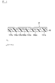
次に、第3の工程に進む。本実施形態の第3工程では、図10に示すように、第2工程で形成された突起30の先端に接続層35を形成する。接続層35は、上述した配線20及び突起30が含む第1金属とは異なる第2金属を含む。第2金属は、第1金属と合金の形成が可能な、第1金属とは異なる金属である。
本実施形態において、接続層35は、突起30の先端部以外をマスクし、第2金属を含む導電性材料で突起30の先端を被覆するめっき工程によって形成することができる。また、第2金属を含む導電性材料を突起30に塗布してその先端を被覆してもよい。さらに、接続層35は、後述するインクジェット印刷工程によって形成することができる。図8又は図9に示す突起30の先端部を第2金属を含む導電性インクの着弾位置として設定し、導電性インクを噴射してもよい。
第3工程において、接続層35に含まれる第2金属は、低融点の金属を選択することが好ましい。例えば、スズ、ビスマス、インジウム、亜鉛、アンチモン及び鉛の群から選択された1種類以上の金属を用いることができる。第2金属は、第1金属とは異なる、ニッケル、鉄、アルミニウム、金、銀及び銅の群から選択された少なくとも1種類以上の金属を、さらに含むことができる。特に限定されないが、本実施形態におけるめっき工程によって突起30の先端部を覆う導電性材料の第2金属は、スズを含むことが好ましい。
なお、上述のスズ、ビスマス、インジウム、亜鉛、アンチモン及び鉛を含む低融点の第2金属の量を増加するほど、加熱プレス時における配線20と突起30との間の合金形成量を増加させることができるので、接合強度がより一層向上し、電気的信頼性を高めることができる。
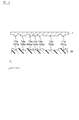
本実施形態において、一の基板6の突起30及び接続層35の高さを、この一の基板6に積層され、突起30及び接続層35が貫通する他の基板6の絶縁性シート10の厚さよりも高くなるように形成する。積層される複数の基板6の厚さが共通する場合には、図10に示すように、突起30と接続層35とを合わせた高さh1を、絶縁性シート10の厚さh2よりも高く形成する。また、後述する第4の工程において積層される基板6の絶縁性シート10の厚さが異なる場合には、突起30及び接続層35の高さ(h1)を、その基板6に積層し、突起30の接続層35が対向する他の基板6の絶縁性シート10の厚さ(図11に示すh2)よりも高く形成する。なお、ここにいう絶縁性シート10の厚さとは、絶縁性シート10の他方主面(配線20が形成されていない面)から配線20の他方主面(絶縁性シート10と接している面)までの長さ、つまり基板6の厚さから配線20の厚さを差し引いた長さである。これにより、積層して熱プレスをしたときに、突起30及び接続層35が積層された基板6の絶縁性シート10を確実に貫通し、突起30の先端部35を基板6の配線20と確実に接触させることができる。
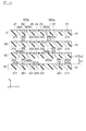
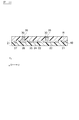
最後に、第4の工程について説明する。先述した第3工程において、配線21~27、突起30及び接続層35が形成された複数枚の基板6(図10)と、配線21~27のみが形成された一枚の基板2(図5)を準備する。そして、図11に示すように、一の基板61の一方主面(突起301a,301bが形成されている面)が他の基板62の他方主面(配線212~272及び突起302a,302bが形成されていない面)に対向するように積層する。同様に基板62の一方主面が他の基板63の他方主面に対向するように積層し、基板63の一方主面が他の基板2の他方主面に対向するように積層する。つまり、最下層を基板61とし、基板62、63をその上に積層し、基板2を最上層に配置する。積層する各基板61~63及び基板2は、画像認識機能付きのアライメント装置により正確に位置合わせが行われる。このとき、各基板61~63及び基板2の配線20のパターンは共通するものであってもよいし、異なるものであってもよい。また各基板61~63の突起30の位置、高さは共通するものであってもよいし、異なるものであってもよい。目的の多層配線板の機能に応じて適宜に設計することができる。
そして、積層した基板61~63及び基板2を加熱し、当該積層方向(図中z方向)に沿って押圧する。熱プレス工程における温度は、絶縁性シート10が軟化して接着性を示す温度とすることができる。熱プレス工程において絶縁性シート10同士は互いに融着又は接着する。特に限定されないが、本実施形態における熱プレス工程の温度は、絶縁性シート10、第1金属と第2金属から得られる合金の融点に応じて、例えば220℃~260℃とすることができる。
各基板61~63の突起301a,301b,302a,302b,303a,303b(以下、突起30と総称することもある)の接続層351a,351b,352a,352b,353a,353b(以下、接続層35と総称することもある)は、加熱によって軟化した絶縁性シート10に押しつけられ、この絶縁性シート10を厚さ方向(図中z方向)に貫通する。
基板61の突起301a及び接続層351a,突起301b及び接続層351bは、基板62の絶縁性シート10を貫通して基板62の配線222と262に基板62の絶縁性シート10の他方主面(図中下側の面)側から圧接される。同じく、基板62の突起302a及び接続層352a,突起302b及び接続層352bは、基板63の絶縁性シート10を貫通して基板63の配線223と263に基板63の絶縁性シート10の他方主面(図中下側の面)側から圧接される。同様に、基板63の突起303a及び接続層353a,突起303b及び接続層353bは、基板2の絶縁性シート10を貫通して基板2の配線22と26(各基板の配線を配線20と総称することもある)に基板2の絶縁性シート10の他方主面(図中下側の面)側から圧接される。圧接された突起30と配線20とは加熱プレスにより密着し、導通可能となる。
加熱プレスの温度条件は、突起30及び配線20に含まれる第1金属と、接続層35に含まれる第2金属とが合金を形成できる温度であるので、突起30と接続層35との間、及び接続層35と配線20との間には合金が形成される。加熱プレスの温度条件は、第1金属と第2金属とが合金を形成することができるように、第1金属、第2金属、又は第1金属と第2金属による合金の融点に基づき、実験的に求めることができる。
なお、絶縁性シート10が熱硬化性樹脂である場合には、絶縁性シート10と突起30及び接続層35が完全に硬化するまで加熱プレスを継続してもよいし、絶縁性シート10が軟化し、絶縁性シート10同士が接着する状態になったら冷却し、その後オーブンで絶縁性シート10、突起30及び接続層35を完全に硬化させてもよい。絶縁性シート10が熱可塑性樹脂である場合には、突起30の接続層35が対向する配線と十分に接合するまでプレスを継続することが好ましい。
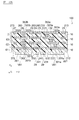
これにより、図12Aに示すように、各基板61~63、基板2の層間導通がされた多層配線板100を、ビアホールを形成する工程を経ることなく得ることができる。
本実施形態の第4工程において、一の基板の一方主面に形成された突起30と他の基板に形成された配線20との間の一領域又は複数の領域に合金が形成される。具体的に、突起301aと接続層351aとの間、突起301bと接続層351bとの間、配線222と接続層351aとの間、配線262と接続層351bとの間には、第1金属と第2金属の合金サイト(合金領域)が形成されている。突起302a、302bと配線223、263との間、突起303a、303b等と配線22、26との間も同様である。
このように、本実施形態の多層配線板の製造方法によれば、第1金属を含む、一の基板の一方主面に形成された突起30及び他の基板に形成された配線20との間に第1金属とは異種金属である第2金属を含む接続層35を介在させるので、熱プレス処理によって突起30と配線20の第1金属と接続層35の第2金属とが反応して合金を含む領域が形成される。これにより、突起30と配線20とを化学的に強固に接合させることができ、接続信頼性の高い多層配線板を製造することができる。
特に限定されないが、第1金属を銅、銀、金のように低抵抗の金属とし、第2金属をスズとすることにより、突起30と配線20の間にCu-Sn,Ag-Sn,Au-Snの合金が形成されるので、電気的特性が良好であるとともに、強固な構造の多層配線板を製造することができる。
本実施形態の多層配線板の製造方法によれば、加熱プレス工程により、積層された絶縁性シート10の主面(一方主面と他方主面)同士が接着するので、絶縁性シート10の間に接着剤を塗る、または接着シートを貼る等により接着層を別途形成する必要がない。このため、積層工程において接着層の形成工程が不要となるので、製造コストを低減させることができる。また、絶縁性シート10の間に接着層を形成しないので、多層配線板100を薄くすることができる。
ビアが形成された基板を一枚ずつ積層していく方法では、各基板にかかる負荷を均等にすることができないため、部分的な変形、特に下層部分に大きな変形が生じる場合がある。これに対し、本実施形態の多層配線板の製造方法は同じ状態の基板6を一括して積層するため、各基板6にかかる負荷を均等にすることができるので、部分的な変形、特に下層部分に大きな変形が生じる事態を防止することができる。
なお、本実施形態の多層配線板の製造方法においては、積層する基板6,2の態様は特に限定されない。例えば、図12Aに示す多層配線板100の最上層に積層された基板2を両面基板に変えることもできる。この場合には、最上層の両面基板と基板63との間に絶縁性シート10を介在させる。また、図12Bに示すように、図12Aに示す多層配線板100の最下層に積層された基板61にビアホールV61と裏面配線29を形成することもできる。この場合には、多層配線板100を形成後に、基板61層にレーザービアホール形成、めっき、エッチング等の従来の配線形成技術を用いて、ビアホールV61と裏面配線29を設けることができる。
<第2実施形態>
次に本発明の第2実施形態に係る多層配線板の製造方法について説明する。本実施形態の製造方法は、第3工程において接続層35をスクリーン印刷により形成する点に特徴が有り、他の部分は第1実施形態の製造方法と共通する。重複した説明を避け、以下には、本実施形態の特徴となる第3工程を中心に説明し、共通する部分については第1実施形態に係る記載を援用する。
次に本発明の第2実施形態に係る多層配線板の製造方法について説明する。本実施形態の製造方法は、第3工程において接続層35をスクリーン印刷により形成する点に特徴が有り、他の部分は第1実施形態の製造方法と共通する。重複した説明を避け、以下には、本実施形態の特徴となる第3工程を中心に説明し、共通する部分については第1実施形態に係る記載を援用する。
図1~5に示す第1実施形態の第1工程と同様に、配線21~27が形成された基板2を準備し、図6、図7に示すようにレジスト層Rに欠損部R1,R2を形成し、めっきにより欠損部R1,R2に第1金属を含む導電性材料を充填する。そして、突起30の形成時にレジスト層Rの表面に析出した金属成分を除去するときに、図13に示すように突起30の先端がレジスト層Rの表面よりも低い位置にまで凹むようにエッチング処理をする。このときに形成された凹部に第2金属を含む導電性ペーストが製版を介して充填されるようにスクリーン印刷し、焼成する。この処理により、図14に示すように、突起30の先端に接続層35を形成することができる。この後に、レジストRを除去すれば、図10に示す基板6を得ることができる。
また、突起30がスクリーン印刷により形成される場合には、第1金属を含む導電性ペーストを用いてスクリーン印刷により突起30を形成し、焼成した後に、第2金属を含む導電性ペーストを用いてスクリーン印刷により接続層35を形成することができる。
この後の第4工程は、第1実施形態と同様である。
このように、本実施形態によれば、第1実施形態と同様の効果を奏するとともに、スクリーン印刷技術を用いることにより、製造コストを低減させ、生産効率を向上させることができる。
<第3実施形態>
次に本発明の第3実施形態に係る多層配線板の製造方法について説明する。本実施形態の製造方法は、第2工程において突起30をインクジェット印刷により形成する点、及び第3工程において接続層35をインクジェット印刷により形成する点に特徴が有り、他の部分は第1実施形態の製造方法と共通する。重複した説明を避け、以下には、本実施形態の特徴となる第2工程及び第3工程を中心に説明し、共通する部分については第1実施形態に係る記載を援用する。
次に本発明の第3実施形態に係る多層配線板の製造方法について説明する。本実施形態の製造方法は、第2工程において突起30をインクジェット印刷により形成する点、及び第3工程において接続層35をインクジェット印刷により形成する点に特徴が有り、他の部分は第1実施形態の製造方法と共通する。重複した説明を避け、以下には、本実施形態の特徴となる第2工程及び第3工程を中心に説明し、共通する部分については第1実施形態に係る記載を援用する。
本実施形態の多層配線板の製造方法は、第1実施形態の図1~5に示す第1工程と同様に、配線21~27が形成された基板2(図5参照)を準備する。
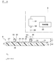
第2工程では、インクジェット方式の印刷装置9を用いて、基板2の配線21~27の所定位置に導電性の突起30を形成する。本実施形態におけるインクジェット方式の印刷装置9は、機能性材料を含む導電性インクの液滴を絶縁性基材の所定領域に向かって吐出し、絶縁性基材の一方主面にパターンを形成する、いわゆるインクジェットプリンタである。図15に示すように、基板2は、本実施形態のインクジェット方式の印刷装置9に、インクジェットヘッド91のノズル92が、配線21~27の所定位置に対向する位置となるようにセットされる。
そして、印刷装置9の制御装置93は、ノズル92から所定位置に向けて導電性インクを複数回吐出する。図15に示すように、インクジェットヘッド91のノズル92から吐出された導電性インクの液滴94は、ノズル92と絶縁性シート10との間の空間を飛翔してノズル92と対向する配線22上の所定位置に着弾する。着弾後のインクの液滴94のインクに含まれる分散材料(溶媒など)が蒸発することにより、配線22上に導電性の機能層が形成される。
なお、本実施形態において突起30の形成に用いられる導電性インクは、粒子径が1μm以下の導電性材料の微粒子や、粒子径が数nm~数十nmの導電性材料のナノ粒子が有機溶媒中に分散されたものを用いることができる。導電性材料が金属の場合は、金属無機塩や有機金属錯体を有機溶媒中に分散させたものであっても構わない。導電性材料としては、金、銀、銅、白金、パラジウム、タングステン、ニッケル、タンタル、ビスマス、鉛、インジウム、スズ、亜鉛、チタン及びアルミニウムの群からなる金属種群のうちの何れか一種若しくは二種以上の金属、又は二種以上の金属からなる合金を用いることができる。さらに、上記金属種群から選択された一種若しくは二種以上の金属の酸化物を含む無機物を導電性材料として用いることもできる。もちろん、上記金属種群から選択された二種以上の金属の合金を導電性材料として用いることもできる。特に限定されないが、本実施形態では、ナノ粒子型の酸化インジウムと酸化スズとの混合インク、その他の金属ナノ粒子を含むインク、又は錯体型の銀などの金属インクを、導電性インクとして用いる。
本実施形態において、配線22上の所定位置に対する導電性インクの吐出は所定周期で、複数回行う。つまり、導電性インクの吐出後、所定時間の経過を待って、さらに導電性インクを吐出する。吐出から吐出までの所定時間においては、所定領域をレーザー照射などにより加温し、導電性インクの溶媒を蒸発させ、基板2の配線21~27の所定位置に着弾した液滴94を乾燥、定着させる。前回吐出した導電性インクが固まった後に、同じ位置に、次の導電性インクを吐出するという動作を繰り返すと、導電性インクが絶縁性シート10の厚さ方向(図中z方向)に沿って積層され、吐出の回数に応じてz方向に伸長した、図15に示す突起30を形成することができる。特に限定されないが、本実施形態における突起30の径(配線22の上面に沿う突起30の太さ)は、2μm以上かつ35μm以下、好ましくは2μm以上かつ15μm以下、さらに好ましくは5μm以上かつ10μm未満である。突起30及び接続層35の高さ(図16のh1を参照)は、導電性インクを吐出する回数により制御することができる。導電性インクの吐出回数と形成される突起30の高さとは、予め実験的に対応づけておくことができる。
そして、導電性インクの特性に応じた条件で焼成処理を行うことにより、導電性の突起30を備える基板6を得ることができる。なお、突起30を形成する際に焼成処理を行うことにより、突起30の硬さを向上させることができる。
次に、第3の工程に進む。本実施形態の第3工程では、図16に示すように、第2工程で形成された突起30の先端に接続層35を形成する。接続層35は、上述した配線20及び突起30が含む第1金属とは異なる第2金属を含む。第2金属は、第1金属と合金の形成が可能な、第1金属とは異なる金属である。
本実施形態において、接続層35は、突起30と同様にインクジェット印刷工程によって形成することができる。先述したインクジェット印刷装置9を用い、突起30の先端位置を導電性インクが着弾する所定位置として設定し、導電性インクの吐出は所定周期で、一回又は複数回行う。突起部30を形成する手法と同様に、導電性インクの吐出後、所定時間の経過を待って、さらに導電性インクを吐出する。吐出から吐出までの所定時間においては、所定領域をレーザー照射などにより加温し、導電性インクの溶媒を蒸発させ、基板2の配線21~27の所定位置に着弾した液滴94を乾燥、定着させることにより、所望の厚さ(高さ)の接続層35を形成することができる。
第3工程において、接続層35に含まれる第2金属は、低融点の金属であることが好ましい。例えば、スズ、ビスマス、インジウム、亜鉛、アンチモン及び鉛の群から選択された1種類以上の金属を用いることができる。第2金属は、第1金属とは異なる、ニッケル、鉄、アルミニウム、金、銀及び銅の群から選択された少なくとも1種類以上の金属を、さらに含むことができる。特に限定されないが、本実施形態における第3工程において突起30の先端部を覆う導電性材料の第2金属は、スズを含むことが好ましい。なお、上述のスズ、ビスマス、インジウム、亜鉛、アンチモン及び鉛を含む低融点の第2金属の量を増加するほど、加熱プレス時における配線20と突起30との間の合金形成量を増加させることができるので、接合強度がより一層向上し、電気的信頼性を高めることができる。
また、インクジェット方式の印刷装置9によって形成された突起30と、その先端に形成される接続層35の形状は、図16に示すように基板2の厚さ方向沿って凸状の曲面で形成される。このように突起30の先端の接続層35を凸状の曲面とすることにより、後述する第4工程において、突起30が他の基板の絶縁性シート10を貫通する際の抵抗を低減させることができる。この結果、突起30の損傷なども防ぐことができる。
本実施形態において、一の基板6の突起30と接続層35の高さを、この一の基板6に積層され、突起30と接続層35が貫通する他の基板6の絶縁性シート10の厚さよりも高くなるように形成する。積層される複数の基板6の厚さが共通する場合には、図16に示すように、突起30の高さh1と接続層35の高さを、絶縁性シート10の厚さh2よりも高くなるように形成する。また、後述する第3の工程において積層される基板6の絶縁性シート10の厚さが異なる場合には、突起30及び接続層35の高さ(h1)を、その基板6に積層され、突起30が対向する他の基板6の絶縁性シート10の厚さ、つまり、突起30と接着層35が貫通する絶縁性シートの厚さ(図17に示すh3)よりも高く(長く)形成する。ここにいう絶縁性シート10の厚さとは、絶縁性シート10の他方主面(配線20が形成されていない面)から配線20の他方主面(絶縁性シート10と接している面)までの長さ、つまり基板6の厚さから配線20の厚さを差し引いた長さである。これにより、積層して熱プレスをしたときに、突起30と接着層35が積層された基板6の絶縁性シート10を確実に貫通し、突起30上に形成された接着層35の先端を基板6の配線20と確実に接触させることができる。
なお、接続層35は、突起30の先端部以外をマスクし、第2金属を含む導電性材料で突起30の先端を被覆するめっき工程によって形成することができる。また、第2金属を含む導電性材料を突起30に塗布してその先端を被覆してもよい。
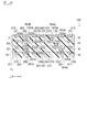
本実施形態の第4の工程について説明する。先述した第3工程において、配線21~27、突起30及び接続層35が形成された複数枚の基板6(図16)と、配線21~27のみが形成された一枚の基板2(図5)を準備する。そして、図17に示すように、一の基板61の一方主面(突起301a,301bが形成されている面)が他の基板62の他方主面(配線212~272及び突起302a,302bが形成されていない面)に対向するように積層する。同様に基板62の一方主面が他の基板63の他方主面に対向するように積層し、基板63の一方主面が他の基板2の他方主面に対向するように積層する。つまり、最下層を基板61とし、基板62、63をその上に積層し、基板2を最上層に配置する。積層する各基板61~63及び基板2は、画像認識機能付きのアライメント装置により正確に位置合わせが行われる。このとき、各基板61~63及び基板2の配線20のパターンは共通するものであってもよいし、異なるものであってもよい。また各基板61~63の突起部30の位置、高さは共通するものであってもよいし、異なるものであってもよい。
本実施形態の第4工程における熱プレス処理は、第1実施形態の第4工程と同様の条件に基づいて行われる。この結果、本実施形態の第4工程において、一の基板の一方主面に形成された突起30と他の基板に形成された配線20との間の一領域又は複数の領域に合金が形成される。具体的に、突起301aと接続層351aとの間、突起301bと接続層351bとの間、配線222と接続層351aとの間、配線262と接続層351bとの間には、第1金属と第2金属の合金サイト(合金領域)が形成されている。突起302a、302bと配線223、263との間、突起303a、303b等と配線22、26との間も同様である。
このように、本実施形態の多層配線板の製造方法によれば、第1金属を含む、一の基板の一方主面に形成された突起30及び他の基板に形成された配線20との間に第1金属とは異種金属である第2金属を含む接続層35を介在させるので、熱プレス処理によって突起30と配線20の第1金属と接続層35の第2金属とが反応して合金を含む領域が形成される。特に、第1金属と第2金属とは合金を形成する組み合わせであるように金属種を選択するので、確実の合金領域を形成することができる。これにより、突起30と配線20とを化学的に強固に接合させることができ、接続信頼性の高い多層配線板を製造することができる。
特に限定されないが、第1金属を銅、銀、金のように低抵抗の金属とし、第2金属をスズとすることにより、突起30と配線20の間にCu-Sn,Ag-Sn,Au-Snの合金が形成されるので、電気的特性が良好であるとともに、強固な構造の多層配線板を製造することができる。加えて本実施形態では、突起30の先端に形成される接続層35を、基板2の厚さ方向(つまり圧接方向)に凸状の曲面とすることができるので、突起30が他の基板の絶縁性シート10を貫通する際の抵抗を低減させ、突起30の損傷なども防ぐことができる。
そして、本実施形態によれば、図18に示すように、各基板61~63、基板2の層間導通がされた多層配線板100を、ビアホールを形成する工程を経ることなく得ることができる。また、第4工程の加熱プレス工程により、積層された絶縁性シート10の主面(一方主面と他方主面)同士が接着するので、絶縁性シート10の間に接着剤を塗る、または接着シートを貼る等により接着層を別途形成する必要がない。このため、積層工程において接着層の形成工程が不要となるので、製造コストを低減させることができる。また、絶縁性シート10の間に接着層を形成しないので、多層配線板100を薄くすることができる。多層配線板100にICチップなどの電子部品を実装する場合においては、低背化を図ることができる。
ビアが形成された基板を一枚ずつ積層していく方法では、各基板にかかる負荷を均等にすることができないため、部分的な変形、特に下層部分に大きな変形が生じる場合がある。これに対し、本実施形態の多層配線板の製造方法は同じ状態の基板6を一括して積層するため、各基板6にかかる負荷を均等にすることができるので、部分的な変形、特に下層部分に大きな変形が生じる事態を防止することができる。
なお、第3実施形態の第3工程において、接続層35をインクジェット印刷工程により形成する手法に代えて、上述しためっき工程又はスクリーン印刷工程により接続層35を形成することもできる。また、第1又は第2実施形態の第3工程において、接続層35を上述しためっき工程又はスクリーン印刷工程により形成する手法に代えて、インクジェット印刷工程により接続層35を形成することもできる。
以上説明した実施形態は、本発明の理解を容易にするために記載されたものであって、本発明を限定するために記載されたものではない。したがって、上記の実施形態に開示された各要素は、本発明の技術的範囲に属する全ての設計変更や均等物をも含む趣旨である。
1…インプリントモールド
11a~17a…版面の凸部
11b~16b…版面の凹部
10…絶縁性シート
101a~107a…凹部
P…導電性材料
R…レジスト層
2,6,61~63…基板
2…基板,配線が形成された基板
6、61~63…基板,配線と突起とが形成された基板(基板2に突起が形成された基板)
20,21~27,29…配線
V61…ビア
30…突起
35…接続層
9…インクジェット方式の印刷装置
91…インクジェットヘッド
92…ノズル
93…制御装置
94…液滴(導電性インクの液滴)
100…多層配線板
11a~17a…版面の凸部
11b~16b…版面の凹部
10…絶縁性シート
101a~107a…凹部
P…導電性材料
R…レジスト層
2,6,61~63…基板
2…基板,配線が形成された基板
6、61~63…基板,配線と突起とが形成された基板(基板2に突起が形成された基板)
20,21~27,29…配線
V61…ビア
30…突起
35…接続層
9…インクジェット方式の印刷装置
91…インクジェットヘッド
92…ノズル
93…制御装置
94…液滴(導電性インクの液滴)
100…多層配線板
Claims (6)
- 絶縁性シートと、前記絶縁性シートの一方主面に埋め込まれ、第1金属を含む導電性の配線とを備える基板を準備する工程と、
前記基板に形成された配線の所定位置に前記第1金属を含む導電性の突起を形成する工程と、
前記突起の先端に前記第1金属とは異なる第2金属を含む接続層を形成する工程と、
前記配線と、前記接続層を有する突起とが形成された複数の前記基板を、前記一の基板の一方主面に形成された突起の接続層が、前記他の基板の他方主面に対向するように積層する工程と、
前記積層した基板を加熱し、当該積層方向に沿って押圧する工程と、を備える多層配線板の製造方法。 - 前記積層した基板を加熱して押圧する工程において、前記接続層と前記突起との間と、前記接続層と前記配線との間とに、前記第1金属と前記第2金属の合金を形成することを特徴とする請求項1に記載の多層配線板の製造方法。
- 前記一の基板に形成された突起及び接続層の高さが、前記一の基板に積層され、前記接続層が対向する前記他の基板の前記絶縁性シートの厚さよりも高いことを特徴とする請求項1に記載の多層配線板の製造方法。
- 前記突起はめっき工程により形成し、前記接続層はめっき工程、スクリーン印刷工程、又はインクジェット印刷工程の何れかの工程により形成することを特徴とする請求項1~3の何れか一項に記載の多層配線板の製造方法。
- 前記突起はスクリーン印刷工程により形成し、前記接続層はめっき工程、スクリーン印刷工程、又はインクジェット印刷工程の何れかの工程により形成することを特徴とする請求項1~3の何れか一項に記載の多層配線板の製造方法。
- 前記突起はインクジェット印刷工程により形成し、前記接続層はめっき工程、スクリーン印刷工程、又はインクジェット印刷工程の何れかの工程により形成することを特徴とする請求項1~3の何れか一項に記載の多層配線板の製造方法。
Applications Claiming Priority (2)
| Application Number | Priority Date | Filing Date | Title |
|---|---|---|---|
| JP2011189585 | 2011-08-31 | ||
| JP2011-189585 | 2011-08-31 |
Publications (1)
| Publication Number | Publication Date |
|---|---|
| WO2013031815A1 true WO2013031815A1 (ja) | 2013-03-07 |
Family
ID=47756295
Family Applications (1)
| Application Number | Title | Priority Date | Filing Date |
|---|---|---|---|
| PCT/JP2012/071806 Ceased WO2013031815A1 (ja) | 2011-08-31 | 2012-08-29 | 多層配線板の製造方法 |
Country Status (2)
| Country | Link |
|---|---|
| TW (1) | TW201320850A (ja) |
| WO (1) | WO2013031815A1 (ja) |
Cited By (2)
| Publication number | Priority date | Publication date | Assignee | Title |
|---|---|---|---|---|
| WO2016114400A1 (ja) * | 2015-01-15 | 2016-07-21 | コニカミノルタ株式会社 | 配線積層構造体及び配線積層構造体の形成方法 |
| WO2017109882A1 (ja) * | 2015-12-24 | 2017-06-29 | 株式会社メイコー | 基板及び基板の製造方法 |
Citations (5)
| Publication number | Priority date | Publication date | Assignee | Title |
|---|---|---|---|---|
| JP2000183528A (ja) * | 1998-12-21 | 2000-06-30 | Ibiden Co Ltd | 多層プリント配線板の製造方法 |
| JP2002329972A (ja) * | 2001-04-27 | 2002-11-15 | Hitachi Metals Ltd | 多層プリント配線基板の製造方法および多層プリント配線基板 |
| JP2006156475A (ja) * | 2004-11-25 | 2006-06-15 | Sohki:Kk | 回路基板の製造方法及び多層配線板の製造方法 |
| JP2006303338A (ja) * | 2005-04-25 | 2006-11-02 | J Macc Co Ltd | 多層回路基板とその製造方法 |
| JP2007165680A (ja) * | 2005-12-15 | 2007-06-28 | Toppan Printing Co Ltd | 積層用配線基板、多層配線基板およびそれらの製造方法、ならびに半導体装置 |
-
2012
- 2012-08-29 WO PCT/JP2012/071806 patent/WO2013031815A1/ja not_active Ceased
- 2012-08-30 TW TW101131478A patent/TW201320850A/zh unknown
Patent Citations (5)
| Publication number | Priority date | Publication date | Assignee | Title |
|---|---|---|---|---|
| JP2000183528A (ja) * | 1998-12-21 | 2000-06-30 | Ibiden Co Ltd | 多層プリント配線板の製造方法 |
| JP2002329972A (ja) * | 2001-04-27 | 2002-11-15 | Hitachi Metals Ltd | 多層プリント配線基板の製造方法および多層プリント配線基板 |
| JP2006156475A (ja) * | 2004-11-25 | 2006-06-15 | Sohki:Kk | 回路基板の製造方法及び多層配線板の製造方法 |
| JP2006303338A (ja) * | 2005-04-25 | 2006-11-02 | J Macc Co Ltd | 多層回路基板とその製造方法 |
| JP2007165680A (ja) * | 2005-12-15 | 2007-06-28 | Toppan Printing Co Ltd | 積層用配線基板、多層配線基板およびそれらの製造方法、ならびに半導体装置 |
Cited By (5)
| Publication number | Priority date | Publication date | Assignee | Title |
|---|---|---|---|---|
| WO2016114400A1 (ja) * | 2015-01-15 | 2016-07-21 | コニカミノルタ株式会社 | 配線積層構造体及び配線積層構造体の形成方法 |
| WO2017109882A1 (ja) * | 2015-12-24 | 2017-06-29 | 株式会社メイコー | 基板及び基板の製造方法 |
| JPWO2017109882A1 (ja) * | 2015-12-24 | 2018-04-19 | 株式会社メイコー | 基板及び基板の製造方法 |
| CN108353498A (zh) * | 2015-12-24 | 2018-07-31 | 名幸电子股份有限公司 | 基板及基板的制造方法 |
| CN108353498B (zh) * | 2015-12-24 | 2020-10-09 | 名幸电子股份有限公司 | 基板及基板的制造方法 |
Also Published As
| Publication number | Publication date |
|---|---|
| TW201320850A (zh) | 2013-05-16 |
Similar Documents
| Publication | Publication Date | Title |
|---|---|---|
| JP5082321B2 (ja) | 多層プリント配線板及びその製造方法 | |
| TWI538579B (zh) | Multi - layer circuit board and multilayer circuit board manufacturing method | |
| US8152953B2 (en) | Method of making printed wiring board and method of making printed circuit board unit | |
| JP5034289B2 (ja) | 多層プリント配線板及びその製造方法 | |
| JP2002359470A (ja) | プリント基板およびその製造方法 | |
| US20090294160A1 (en) | Method of making printed wiring board and electrically-conductive binder | |
| US8143529B2 (en) | Laminated multi-layer circuit board | |
| JP2012079994A (ja) | 部品内蔵プリント配線板およびその製造方法 | |
| WO2007114111A1 (ja) | 多層配線基板とその製造方法 | |
| JP2007266196A (ja) | 多層プリント配線板及びその製造方法 | |
| JP2013512581A (ja) | プリント回路基板及びその製造方法 | |
| US20170034911A1 (en) | Resin multilayer substrate and method of manufacturing the same | |
| WO2013031815A1 (ja) | 多層配線板の製造方法 | |
| JP6058321B2 (ja) | 配線基板の製造方法 | |
| JP2016219452A (ja) | 多層基板及び多層基板の製造方法 | |
| CN104684249A (zh) | 印刷配线板及其制造方法 | |
| JP3956087B2 (ja) | プリント基板の製造方法 | |
| JP2012169486A (ja) | 基材、配線板、基材の製造方法及び配線板の製造方法 | |
| JP2013051367A (ja) | 多層配線板の製造方法 | |
| JP2005251949A (ja) | 配線基板及びその製造方法 | |
| JP2013211344A (ja) | 多層配線板の製造方法 | |
| KR100619512B1 (ko) | 배선층을 갖는 기판 및 그 제조방법 | |
| JP2002374068A (ja) | 多層プリント配線板の製造方法 | |
| JP2014130919A (ja) | 多層プリント配線基板及びその製造方法 | |
| JP2009043917A (ja) | 多層配線板及びその製造方法 |
Legal Events
| Date | Code | Title | Description |
|---|---|---|---|
| 121 | Ep: the epo has been informed by wipo that ep was designated in this application |
Ref document number: 12826781 Country of ref document: EP Kind code of ref document: A1 |
|
| NENP | Non-entry into the national phase |
Ref country code: DE |
|
| 122 | Ep: pct application non-entry in european phase |
Ref document number: 12826781 Country of ref document: EP Kind code of ref document: A1 |
|
| NENP | Non-entry into the national phase |
Ref country code: JP |