WO2013024711A1 - チューナモジュール、回路基板、及び回路基板の組立方法 - Google Patents
チューナモジュール、回路基板、及び回路基板の組立方法 Download PDFInfo
- Publication number
- WO2013024711A1 WO2013024711A1 PCT/JP2012/069808 JP2012069808W WO2013024711A1 WO 2013024711 A1 WO2013024711 A1 WO 2013024711A1 JP 2012069808 W JP2012069808 W JP 2012069808W WO 2013024711 A1 WO2013024711 A1 WO 2013024711A1
- Authority
- WO
- WIPO (PCT)
- Prior art keywords
- circuit board
- tuner module
- tuner
- leg
- hole
- Prior art date
- Legal status (The legal status is an assumption and is not a legal conclusion. Google has not performed a legal analysis and makes no representation as to the accuracy of the status listed.)
- Ceased
Links
Images


Classifications
-
- H—ELECTRICITY
- H05—ELECTRIC TECHNIQUES NOT OTHERWISE PROVIDED FOR
- H05K—PRINTED CIRCUITS; CASINGS OR CONSTRUCTIONAL DETAILS OF ELECTRIC APPARATUS; MANUFACTURE OF ASSEMBLAGES OF ELECTRICAL COMPONENTS
- H05K7/00—Constructional details common to different types of electric apparatus
- H05K7/02—Arrangements of circuit components or wiring on supporting structure
- H05K7/026—Multiple connections subassemblies
-
- H—ELECTRICITY
- H05—ELECTRIC TECHNIQUES NOT OTHERWISE PROVIDED FOR
- H05K—PRINTED CIRCUITS; CASINGS OR CONSTRUCTIONAL DETAILS OF ELECTRIC APPARATUS; MANUFACTURE OF ASSEMBLAGES OF ELECTRICAL COMPONENTS
- H05K3/00—Apparatus or processes for manufacturing printed circuits
- H05K3/30—Assembling printed circuits with electric components, e.g. with resistors
- H05K3/306—Assembling printed circuits with electric components, e.g. with resistors with lead-in-hole components
- H05K3/308—Adaptations of leads
-
- H—ELECTRICITY
- H04—ELECTRIC COMMUNICATION TECHNIQUE
- H04M—TELEPHONIC COMMUNICATION
- H04M7/00—Arrangements for interconnection between switching centres
-
- H—ELECTRICITY
- H05—ELECTRIC TECHNIQUES NOT OTHERWISE PROVIDED FOR
- H05K—PRINTED CIRCUITS; CASINGS OR CONSTRUCTIONAL DETAILS OF ELECTRIC APPARATUS; MANUFACTURE OF ASSEMBLAGES OF ELECTRICAL COMPONENTS
- H05K13/00—Apparatus or processes specially adapted for manufacturing or adjusting assemblages of electric components
- H05K13/04—Mounting of components, e.g. of leadless components
-
- H—ELECTRICITY
- H01—ELECTRIC ELEMENTS
- H01R—ELECTRICALLY-CONDUCTIVE CONNECTIONS; STRUCTURAL ASSOCIATIONS OF A PLURALITY OF MUTUALLY-INSULATED ELECTRICAL CONNECTING ELEMENTS; COUPLING DEVICES; CURRENT COLLECTORS
- H01R12/00—Structural associations of a plurality of mutually-insulated electrical connecting elements, specially adapted for printed circuits, e.g. printed circuit boards [PCB], flat or ribbon cables, or like generally planar structures, e.g. terminal strips, terminal blocks; Coupling devices specially adapted for printed circuits, flat or ribbon cables, or like generally planar structures; Terminals specially adapted for contact with, or insertion into, printed circuits, flat or ribbon cables, or like generally planar structures
- H01R12/70—Coupling devices
- H01R12/71—Coupling devices for rigid printing circuits or like structures
- H01R12/712—Coupling devices for rigid printing circuits or like structures co-operating with the surface of the printed circuit or with a coupling device exclusively provided on the surface of the printed circuit
- H01R12/716—Coupling device provided on the PCB
-
- H—ELECTRICITY
- H01—ELECTRIC ELEMENTS
- H01R—ELECTRICALLY-CONDUCTIVE CONNECTIONS; STRUCTURAL ASSOCIATIONS OF A PLURALITY OF MUTUALLY-INSULATED ELECTRICAL CONNECTING ELEMENTS; COUPLING DEVICES; CURRENT COLLECTORS
- H01R24/00—Two-part coupling devices, or either of their cooperating parts, characterised by their overall structure
- H01R24/38—Two-part coupling devices, or either of their cooperating parts, characterised by their overall structure having concentrically or coaxially arranged contacts
- H01R24/40—Two-part coupling devices, or either of their cooperating parts, characterised by their overall structure having concentrically or coaxially arranged contacts specially adapted for high frequency
- H01R24/50—Two-part coupling devices, or either of their cooperating parts, characterised by their overall structure having concentrically or coaxially arranged contacts specially adapted for high frequency mounted on a PCB [Printed Circuit Board]
-
- H—ELECTRICITY
- H05—ELECTRIC TECHNIQUES NOT OTHERWISE PROVIDED FOR
- H05K—PRINTED CIRCUITS; CASINGS OR CONSTRUCTIONAL DETAILS OF ELECTRIC APPARATUS; MANUFACTURE OF ASSEMBLAGES OF ELECTRICAL COMPONENTS
- H05K1/00—Printed circuits
- H05K1/02—Details
- H05K1/14—Structural association of two or more printed circuits
- H05K1/141—One or more single auxiliary printed circuits mounted on a main printed circuit, e.g. modules, adapters
-
- H—ELECTRICITY
- H05—ELECTRIC TECHNIQUES NOT OTHERWISE PROVIDED FOR
- H05K—PRINTED CIRCUITS; CASINGS OR CONSTRUCTIONAL DETAILS OF ELECTRIC APPARATUS; MANUFACTURE OF ASSEMBLAGES OF ELECTRICAL COMPONENTS
- H05K2201/00—Indexing scheme relating to printed circuits covered by H05K1/00
- H05K2201/10—Details of components or other objects attached to or integrated in a printed circuit board
- H05K2201/10007—Types of components
- H05K2201/10189—Non-printed connector
-
- H—ELECTRICITY
- H05—ELECTRIC TECHNIQUES NOT OTHERWISE PROVIDED FOR
- H05K—PRINTED CIRCUITS; CASINGS OR CONSTRUCTIONAL DETAILS OF ELECTRIC APPARATUS; MANUFACTURE OF ASSEMBLAGES OF ELECTRICAL COMPONENTS
- H05K2201/00—Indexing scheme relating to printed circuits covered by H05K1/00
- H05K2201/10—Details of components or other objects attached to or integrated in a printed circuit board
- H05K2201/10227—Other objects, e.g. metallic pieces
- H05K2201/10371—Shields or metal cases
-
- H—ELECTRICITY
- H05—ELECTRIC TECHNIQUES NOT OTHERWISE PROVIDED FOR
- H05K—PRINTED CIRCUITS; CASINGS OR CONSTRUCTIONAL DETAILS OF ELECTRIC APPARATUS; MANUFACTURE OF ASSEMBLAGES OF ELECTRICAL COMPONENTS
- H05K2201/00—Indexing scheme relating to printed circuits covered by H05K1/00
- H05K2201/10—Details of components or other objects attached to or integrated in a printed circuit board
- H05K2201/10613—Details of electrical connections of non-printed components, e.g. special leads
- H05K2201/10742—Details of leads
- H05K2201/1075—Shape details
- H05K2201/10803—Tapered leads, i.e. leads having changing width or diameter
-
- H—ELECTRICITY
- H05—ELECTRIC TECHNIQUES NOT OTHERWISE PROVIDED FOR
- H05K—PRINTED CIRCUITS; CASINGS OR CONSTRUCTIONAL DETAILS OF ELECTRIC APPARATUS; MANUFACTURE OF ASSEMBLAGES OF ELECTRICAL COMPONENTS
- H05K3/00—Apparatus or processes for manufacturing printed circuits
- H05K3/0008—Apparatus or processes for manufacturing printed circuits for aligning or positioning of tools relative to the circuit board
-
- Y—GENERAL TAGGING OF NEW TECHNOLOGICAL DEVELOPMENTS; GENERAL TAGGING OF CROSS-SECTIONAL TECHNOLOGIES SPANNING OVER SEVERAL SECTIONS OF THE IPC; TECHNICAL SUBJECTS COVERED BY FORMER USPC CROSS-REFERENCE ART COLLECTIONS [XRACs] AND DIGESTS
- Y10—TECHNICAL SUBJECTS COVERED BY FORMER USPC
- Y10T—TECHNICAL SUBJECTS COVERED BY FORMER US CLASSIFICATION
- Y10T29/00—Metal working
- Y10T29/49—Method of mechanical manufacture
- Y10T29/49002—Electrical device making
- Y10T29/49117—Conductor or circuit manufacturing
- Y10T29/49124—On flat or curved insulated base, e.g., printed circuit, etc.
- Y10T29/4913—Assembling to base an electrical component, e.g., capacitor, etc.
Definitions
- the present disclosure relates to a tuner module, a circuit board, and a method for assembling the circuit board, and more particularly to a technique for automatically mounting a module device such as a tuner module on a circuit board.
- a conventional tuner is a metal can structure in which a circuit board 1 is covered with a chassis angle 8 and a shield lid 9 as shown in FIG.
- a power source and a signal are connected to an external circuit using the pin header 25 shown.
- the tuner is fixed and mounted on the main board 6 by connecting the chassis legs 8a of the tuner, the feedthrough capacitor 4, and the pin header 25 to the main board 6 on which the tuner is mounted.
- These tuners have a large number of coils and chip parts inside, and have a shield lid 9 and a metal part having a complicated chassis angle as shown in FIG.
- tuner mount operators are indispensable for tuner production.
- soldering is indispensable as an electrical connection method that can ensure high-frequency contact resistance for the connection between the chassis feet and the main board.
- the chassis foot is also a part of the chassis angle, heat conductivity is high, and in order for the chassis foot to be soldered under good soldering conditions, a solder heating method with a high heat capacity is required.
- a dip method in which the main board is hidden in the solder layer while avoiding mounting components on the opposite side of the tuner mounting surface on the main board.
- the solder spray surface (the surface on which the tuner is not mounted) is at a high temperature, so it is basically impossible to arrange the components. Further, in the local reflow method, it is necessary to partially blow out or set the position of the nozzle in accordance with the shape of the tuner, the chassis foot, and the position of the feedthrough capacitor. In other words, since it is necessary to reset the nozzles in accordance with the tuner modification or model switching accompanying the change of the main board, there is a problem that requires a great number of man-hours for switching the production line.
- tuner module can be reduced in thickness, and the total weight of the tuner module can be greatly reduced. That is, a tuner module having a weight of 50 grams or less has been developed, and in terms of weight, an adsorption load can be applied by an automatic insertion device.
- an automatic insertion terminal has a deformed insertion terminal structure. That is, the pin header mounted on the main board that is locked to the chassis angle of the press part by soldering or the like and a part of the chassis angle become a joint part of the main board.
- the first design items often determine the soldering gap, the reliability of the solder joint, and the ease of assembly. Provide an appropriate gap between elements. Therefore, the terminal where the finally assembled tuner module is joined to the main board has a considerable tolerance. Since this tolerance is about 0 ⁇ 0.5 mm in a normal design, it is not suitable for automatic insertion by an automatic insertion device.
- This disclosure has been made in consideration of the above-described situation, and significantly improves the work efficiency when the tuner module is mounted on the main board (circuit board body).
- the present disclosure is configured to have a signal terminal electrically connected to the circuit board body and at least one leg longer than the length of the signal terminal on a surface of the tuner module facing the circuit board body.
- a tip end portion formed with a taper of the first leg protruding from the tuner module main body is formed on the circuit board main body. It inserts in the formed 1st hole.
- the tip portion protruding from the tuner module main body and having the taper of the second leg shorter than the first leg is inserted into the second hole formed in the circuit board main body.
- a signal terminal shorter than the second leg protruding from the tuner board is inserted into a third hole formed in the circuit board body.
- the ease of mounting the tuner module on the circuit board body is improved, and the working efficiency is remarkably improved. Therefore, it can be applied to the automatic insertion of the tuner module into the circuit board main body.
- FIG. 1 is an external perspective view illustrating an example of a tuner module according to an embodiment of the present disclosure. It is the front view which looked at the tuner module from the antenna connector side. It is the rear view which looked at the tuner module from the opposite side to the antenna connector side. It is explanatory drawing which shows the result of having investigated the readability by the combination of the color of a recognition mark and a LED light source. It is the perspective view which showed the tuner module and the circuit board main body. It is the perspective view which looked at the tuner module mounted in the circuit board main body from the back surface of the circuit board main body.
- FIG. 6 is a back view illustrating an example of a positional relationship between a guide terminal, a reinforcing terminal, and a signal terminal of a tuner module according to a modification of an embodiment of the present disclosure.
- One embodiment (guide terminal: an example in which a guide terminal longer than the signal terminal and the reinforcing terminal is separated from the signal terminal) 1-1.
- Circuit board assembly method (example of inserting the guide terminal, reinforcing terminal and signal terminal of the tuner module into the corresponding holes of the circuit board body) 2.
- Modification (Guide terminal: An example in which all signal terminals are surrounded by guide terminals)
- FIG. 1 is a block diagram illustrating a configuration example of a tuner module mounting apparatus.
- the tuner module mounting device 3 is a device that places the tuner module 1 at a prescribed position on the circuit board body 2 and mounts the tuner module 1 on the circuit board body 2.
- the tuner module mounting apparatus 3 mainly includes a suction head 4, a camera 5, an illumination unit 5 ⁇ / b> A, a control unit 6, a drive unit 7, and a vacuum processing unit 8.
- the suction head 4 has a cylindrical hollow inside and is attached to an arm (not shown) connected to the drive unit 7.
- the tip of the suction head 4 is brought into contact with the upper surface of the tuner module 1, and the vacuum processing unit 8 is operated to bring the tip and the contact portion of the tuner module 1 into a vacuum state.
- the tuner module 1 is adsorbed.
- the arm is moved in a state where the tuner module 1 is sucked to the tip of the suction head 4, and the tuner module 1 is moved to a target position.
- the camera 5 is attached to the arm of the suction head 4 as an example, and is an imaging unit for optical position measurement.
- the part (the tuner module 1 in this example) and the circuit board body 2 that the suction head 4 sucks are photographed.
- the illumination unit 5 ⁇ / b> A illuminates light of a light amount necessary for the camera 5 to photograph the tuner module 1 and the circuit board body 2.
- a light emitting diode (LED) can be used in the illumination unit 5A.
- the control unit 6 mainly includes an image processing unit 6a, an arithmetic processing unit 6b, and a position adjusting unit 6c.
- the image processing unit 6a performs predetermined processing such as binarization on the image signal including the information of the subject photographed by the camera 5, and then outputs the image signal to the arithmetic processing unit 6b.
- the arithmetic processing unit 6 b acquires the current position information of the suction head 4 from the signal supplied from the driving unit 7.
- the arithmetic processing unit 6b calculates the positional relationship and the amount of displacement between the circuit board body 2 and the suction head 4 from the information based on the image signal supplied from the image processing unit 6a and the current position information of the suction head 4, Control is performed so as to output the calculation result to the position adjusting unit 6c. Further, the arithmetic processing unit 6 b controls the vacuum processing unit 8 to operate so that the tuner module 1 is sucked to the tip of the suction head 4. The position adjustment unit 6c outputs a drive signal to the drive unit 7 based on the calculation result supplied from the arithmetic processing unit 6b.
- the driving unit 7 operates based on the control signal from the position adjusting unit 6c, and moves the arm connected to the suction head 4.
- the vacuum processing unit 8 performs evacuation based on the control signal from the arithmetic processing unit 6b, and makes the atmosphere of the contact portion between the tip of the suction head 4 and the parts such as the tuner module 1 into a vacuum state.
- the tip of the suction head 4 sucks parts using vacuum, but a silicon suction part is provided at the tip and the parts are sucked by the silicon suction part. Good. In that case, the vacuum processing unit 8 becomes unnecessary.
- the control unit 6 of the tuner module mounting apparatus 3 controls the drive signal supplied from the arithmetic processing unit 6b to the position adjustment unit 6c and supplied to the drive unit 7 so that the tip of the suction head 4 is at an appropriate position or It is brought into contact with the upper surface of the target tuner module 1 stored in a tray (not shown).
- the arithmetic processing unit 6b of the control unit 6 controls the camera 5 to photograph the tip of the tuner module 1 and the suction head 4, and confirms the positional relationship between the two by the image supplied from the image processing unit 6a.
- the arithmetic processing unit 6b issues an instruction to the position adjustment unit 6c and controls the drive unit 7 to change the position of the suction head 4. It adjusts and it controls so that the front-end
- the arithmetic processing unit 6 b of the control unit 6 operates the vacuum processing unit 8 to suck the tuner module 1 at the tip of the suction head 4 and outputs a control signal to the drive unit 7 to connect to the suction head 4. To move the tuner module 1 to a predetermined mounting position of the circuit board main body 2.
- the arithmetic processing unit 6b of the control unit 6 controls the camera 5 to photograph the tip of the tuner module 1 and the suction head 4, and from the image supplied from the image processing unit 6a to the position where the circuit board body 2 is to be mounted.
- the tuner module 1 is mounted.
- the arithmetic processing unit 6b confirms the position of the tuner module 1 on the circuit board body 2 with reference to the alignment marks 2a to 2c provided on the circuit board body 2, and determines the tuner module 1 in the correct position. To implement.
- FIG. 2 is an external perspective view illustrating an example of a tuner module according to an embodiment of the present disclosure.
- FIG. 3 is a front view of the tuner module 1 of FIG. 2 as viewed from the antenna connector side.
- FIG. 4 is a rear view of the tuner module 1 as viewed from the side opposite to the antenna connector side.
- the present disclosure has a configuration in which a signal terminal electrically connected to the circuit board body 2 and at least one leg longer than the length of the signal terminal are provided on a surface of the tuner module 1 facing the circuit board body 2. Is.
- the tuner module 1 has biaxial antenna connectors 51 and 52 on the front part.
- the antenna connectors 51 and 52 are locked to one side surface of the tuner case 20 by a caulking structure.
- the tuner case 20 includes a tuner substrate 10, and the bottom and top surfaces of the tuner case 20 are covered with a base 30 and a cover 40, respectively.
- the tuner case 20, the base 30, and the cover 40 are an example of a tuner module main body.
- a pin header for connecting to the outside of the tuner module 1 is mounted together with an element group such as an IC (not shown) constituting the tuner circuit.
- the ground portion of the tuner board 10 is electrically connected to the tuner case 20. Connected.
- a recognition mark 41 is provided at a balance point (preferably a center of gravity) of the weight of the tuner module 1 as a whole.
- the recognition mark 41 is provided at a predetermined position of the cover 40 when the suction head 4 sucks up the main body of the tuner module 1, that is, when the main body of the tuner module 1 is viewed from the upper surface.
- This recognition mark 41 is a target point that is aimed to be lifted while maintaining the horizontal position when the suction head 4 of the tuner module mounting apparatus 3 comes into contact with the tuner module 1 and sucks it. It is also an authentication point for optically reading tolerances.
- the recognition mark 41 reflects the light emitted from the illumination unit 5A such as an LED so that the position can be read. It is written.
- the recognition mark 41 will be described.
- the material of the tuner case 20 and the cover 40 of the tuner module 1 is made of metal, various reflections occur depending on the emission color of the LED. Therefore, the recognition mark 41 is preferably marked with a color that absorbs light, such as black.
- the cover 40 is formed by bending a general tin-plated steel material called tinplate in a press process, when a black mark is printed, a new process is required separately from the press process. This causes an increase in cost including assembly of a circuit board, that is, a significant complexity and an increase in tact time. Therefore, in the present disclosure, the recognition mark 41 is provided with a small protrusion that can be created in the same process as the pressing of the cover 40, so that work such as coloring can be deleted.
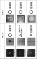
- FIG. 5 is an explanatory diagram showing the results of examining whether or not reading is possible depending on the combination of the recognition mark and the color of the LED light source.
- the aperture shape of ⁇ 0.8, 2 mm square engraved shape (cross-girder pattern), and press processing (surface processing) of ⁇ 2.0 can be read using the light of white LED and red LED. Checked if possible.
- the small protrusion shape by the drawing process was recognizable by both the white LED and the red LED.
- the red LED is recognized very well as compared with the multi-stamp mark and the press mark. This is achieved by the fact that the light reflecting the light from the LED light source does not easily reach the camera 5 installed at a position close to the incident direction.
- a chassis leg structure suitable for automatic insertion will be described with reference to a rear view of the tuner module 1 of FIG. 4 viewed from the side opposite to the antenna connector side.
- a pin header (not shown) having a plurality of signal terminals (pins) 11 is an integrated body mounted on the tuner board 10, but when viewed from the outside of the tuner module 1, it is divided into a group of two signal terminals 11. appear.
- a guide terminal 21-1 having a length A (leg part: an example of a first leg part) and a reinforcing terminal 22- having a length B are provided.
- the guide terminal 21-1 protrudes from the tuner module main body (tuner case 20) and is formed near the center of the back surface portion.
- the reinforcing terminals 22-4 and 22-5 are ground terminals for connecting to the ground potential of the circuit board body 2 and reinforce the fixing strength of the solder joint between the signal terminal 11 and the circuit board body 2.
- the tuner module main body (tuner case 20) protrudes from both ends of the back surface portion.
- the signal terminal 11 protrudes from the tuner substrate 10 and extends to the back surface portion.
- the lengths A, B, and C of the guide terminal, the reinforcing terminal, and the signal terminal are: A> B ⁇ C To have a relationship.
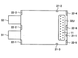
- FIG. 6 is a perspective view showing the tuner module 1 and the circuit board main body 2.
- FIG. 7 is a perspective view of the tuner module 1 mounted on the circuit board body 2 as seen from the back surface of the circuit board body 2.
- the circuit board body 2 constitutes a receiving circuit of a television set, for example, and is mounted with components other than the tuner.
- a hole (first hole) for inserting a guide terminal provided in the tuner module 1 described above, a hole (second hole) for inserting a reinforcing terminal, and a signal terminal are inserted. Hole (third hole) is provided.
- guide terminals 21-1 to 21-3, reinforcing terminals 22-1 to 22-5, and signal terminals 11 are provided on the side of the tuner module 1 facing the circuit board body 2. It protrudes.
- insertion holes 61-1 to 61-3 for guide terminals and solder joint holes 62-1 to 62-1 for reinforcing terminals are formed in the circuit board body 2.
- 62-5 a plurality of solder joint holes 64 for signal terminals are formed.
- the base 30 is provided with openings 32U1 and 32U2, and the signal terminal 11 of the pin header mounted on the tuner board 10 is configured to protrude outside the base 30. Further, for example, holes 63-1 to 63-4 for mounting to the television set by screwing or the like after mounting the tuner module 1 are formed.
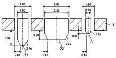
- FIG. 8 is an explanatory diagram showing a clearance (clearance) between the guide terminal, the reinforcing terminal, and the signal terminal of the tuner module 1 and the corresponding hole of the circuit board main body.
- FIG. 8 is simplified and schematically shown in order to explain the function of each terminal.
- each terminal of the tuner module 1 For the purpose of enhancing the ease of inserting each terminal of the tuner module 1 into each hole of the circuit board body 2, the relationship between the diameter of each terminal and the diameter of each hole is set as follows. (1) Clearance between the guide terminal 21 and the insertion hole: large (2) Clearance between the reinforcement terminal 22 and the insertion hole: For the small signal terminal 11, a joint hole is inserted at the same time as the reinforcement terminal is finally inserted into the insertion hole. It can be set within the following range. (3) Clearance between signal terminal 11 and joint hole: More than the clearance in (2) above
- the tip of each terminal is formed in a tapered shape.
- the guide terminal 21 has a tapered portion 21 s
- the reinforcing terminal 22 has a tapered portion 22 s
- the signal terminal 11 has a tapered portion 11 s.
- the tapered portions of the guide terminal 21 and the reinforcing terminal 22 are essential, but the tapered portion of the signal terminal 11 is not necessarily required.
- the shape of each tip may be a curved surface instead of a taper, and may be a right angle or an acute angle.
- the thickness of the circuit board body 2 is 1.2 to 1.6 mm as an example.
- the clearance between the guide terminal 21 and the insertion hole is 0.30 mm
- the distance between the cut-out point of the tapered portion 21s and the insertion hole is 0.60 mm
- the length of the portion protruding from the circuit board body 2 is 1.50 mm.
- the clearance between the reinforcing terminal 22 and the insertion hole is 0.15 mm
- the distance between the cut-out point of the tapered portion 22 s and the insertion hole is 0.45 mm
- the length of the portion protruding from the circuit board body 2 is 0.90 mm.
- the clearance between the signal terminal 11 and the insertion hole is 0.35 mm, the distance between the cut-out point of the tapered portion 11s and the insertion hole is 0.45 mm, and the length of the portion protruding from the circuit board body 2 is 0.30 mm.
- FIGS. 9A, 9B, and 9C are explanatory views showing a process until the signal terminal 11 of the tuner module 1 is inserted into the solder joint hole 64 of the circuit board main body 2.
- 8 shows a process in which the tuner module 1 at a position slightly deviated from the hole position is lowered toward the circuit board body 2 while maintaining the relationship between the guide terminal 21, the reinforcing terminal 22 and the signal terminal 11 in FIG. ing.
- the suction head 4 of the tuner module mounting device 3 has some flexibility to move left and right, when the tuner module 1 is lifted by sucking the recognition mark 41 and lowered toward the circuit board main body 2, the guide terminal is initially used. 21 tapered portions 21 s contact the edge of the insertion hole 61 on the surface of the circuit board body 2. As the guide terminal 21 is guided into the insertion hole 61 along the tapered portion 21s, the guide terminal 21 is slightly shifted in the left direction in the drawing (FIG. 9A).
- the reinforcing terminal 22 is first tapered at a position shifted to the left side by the amount of displacement of the guide terminal 21. 22 s contacts the edge of the solder joint hole 62 on the surface of the circuit board body 2. The reinforcing terminal 22 is inserted into the solder joint hole 62 along the tapered portion 22s, and is inserted even if the clearance between the reinforcing terminal 22 and the solder joint hole 62 is narrow (FIG. 9B).
- the reinforcing terminal 22 formed of the tuner case 20 which is the same part as the guide terminal 21 is provided with a solder joint hole 62 as small as possible so that the guide terminal 21 has a clearance that can be corrected.
- the signal terminal 11 has a play in which the insertion tolerance between the pin header and the tuner board 10, the assembly tolerance between the tuner board 10 and the tuner case 20, and the clearance between the reinforcing terminal 22 and the solder joint hole 62 are all added. It is inserted into the solder joint hole 64 having a dimension taken into account.
- the ease of mounting the tuner module 1 on the circuit board body 2 is improved, and the working efficiency is remarkably improved. Therefore, it can be applied to the automatic insertion of the tuner module 1 into the circuit board body 2, that is, the tuner module mounting process of the tuner module mounting apparatus.
- FIG. 10 is a back view illustrating an example of the positional relationship between the guide terminal, the reinforcement terminal, and the signal terminal of the tuner module according to a modification of the embodiment of the present disclosure.
- the plurality of guide terminals be disposed so as to surround the signal terminal 11 having the largest manufacturing tolerance in theory for mounting the board. It is convenient that at least all the signal terminals 11 are sandwiched between the plurality of guide terminals 21-1 to 21-3, and the reinforcing terminals 22-1 to 22-6 and all the signal terminals 11 are arranged at approximately equal distances. .
- the three guide terminals are arranged so that all the signal terminals 11 are included within the range of the vertical and horizontal projection widths (Ferret diameter) of the three guide terminals.
- the positions of the plurality of guide terminals with respect to the signal terminals may be set according to the area (or weight balance) of the surface of the tuner module 1 facing the circuit board body 2.
- the guide terminal 21-2 is arranged closer to the antenna connector side than the signal terminal 11 side. .
- the reinforcing terminal is soldered to the circuit board body after being inserted into the insertion hole of the circuit board body.
- the guide terminal is also soldered to the circuit board body after being inserted into the insertion hole of the circuit board body. You may be made to do. That is, a part of each function of the guide terminal and the reinforcing terminal is shared. In this case, since the total number of guide terminals and reinforcing terminals can be reduced, the structure of the tuner case can be simplified and the material cost can be reduced.
- the technical idea of the present disclosure is such that a signal terminal electrically connected to the circuit board main body and at least one leg longer than the length of the signal terminal are provided on a surface of the tuner module facing the circuit board main body.
- the above-described guide terminal and reinforcing terminal of the tuner module may be a plurality of terminals (leg portions) having the same length longer than the signal terminal. Then, the signal terminal is inserted into a predetermined hole of the circuit board body using this leg portion and inserted, and after the insertion, the leg portion is soldered to the circuit board body.
- at least one guide terminal or reinforcement terminal longer than the signal terminal may be provided to ensure ease of insertion into the circuit board body.
- this indication can also take the following structures.
- a tuner module body containing a tuner board; A first leg protruding from the tuner module body and inserted into a first hole formed in the circuit board body; A second leg that protrudes from the tuner module body and is inserted into a second hole formed in the circuit board body; the second leg being shorter than the first leg; A signal terminal that protrudes from the tuner board and is inserted into a third hole formed in the circuit board main body, and shorter than the second leg.
- a taper is formed at least at the tip of the first leg and the second leg.
- any one of (1) to (3) Tuner module described in (5) The tuner module according to (4), wherein the plurality of first legs are arranged so that the signal terminals are included in a range of vertical and horizontal projection widths of the plurality of first legs. (6) At least one first leg portion among the plurality of first leg portions is disposed at a position away from the signal terminal by a distance between the other first leg portion and the signal terminal. The tuner module described in 5). (7) The signal terminal is solder-bonded to the circuit board body after being inserted into the third of the circuit board body, The tuner module according to any one of (1) to (6), wherein the second leg portion is inserted into the second hole of the circuit board body and then soldered to the circuit board body.
- the tuner module according to (7) wherein the first leg is soldered to the circuit board body after being inserted into the first hole of the circuit board body.
- a tuner module body containing a tuner board; At least one leg projecting from the tuner module body and inserted into a hole formed in the circuit board body; A signal terminal that protrudes from the tuner board and is inserted into a hole different from the hole formed in the circuit board body; A tuner module, wherein a recognition mark which is a target when the tuner module main body is attracted is provided on the upper surface of the tuner module main body, and a taper is formed at least at the tip of the leg portion.
- a circuit board body (12) a circuit board body; A tuner module body containing the tuner board; A first leg protruding from the tuner module body and inserted into a first hole formed in the circuit board body; A second leg that protrudes from the tuner module body and is inserted into a second hole formed in the circuit board body; the second leg being shorter than the first leg; A signal terminal that protrudes from the tuner board and is inserted into a third hole formed in the circuit board body, and is shorter than the second leg part. At least the first leg part and the tip part of the second leg part are tapered. Is formed.
- a tip portion formed with a taper of the first leg protruding from the tuner module main body is formed on the circuit board main body. Inserting into the first hole; Inserting a tip portion protruding from the tuner module main body and having a second leg taper shorter than the first leg portion into a second hole formed in the circuit board main body; Inserting a signal terminal shorter than the second leg protruding from the tuner board into a third hole formed in the circuit board body.
- processing steps describing time-series processing are not limited to processing performed in time series according to the described order, but are not necessarily processed in time series, either in parallel or individually. This includes processing executed in parallel (for example, parallel processing or processing by an object).
- the present disclosure is not limited to each of the above-described embodiments, and various other modifications and application examples can be taken without departing from the gist described in the claims. . That is, the examples of the above-described embodiments are preferable specific examples of the present disclosure, and thus various technically preferable limitations are given. However, the technical scope of the present disclosure is not limited to these forms unless specifically described in each description to limit the present disclosure.
- the materials used in the following description, the amounts used, the processing time, the processing order, and the numerical conditions of each parameter are only suitable examples, and the dimensions, shapes, and arrangement relationships in the drawings used for the description are also outline. Is something.
- the tuner module is configured by the tuner case that holds the tuner substrate, the base that covers the bottom surface and the top surface of the tuner case, and the cover.
- the tuner module may have a simple configuration that does not use a base and a cover.
- the tuner case is formed in a frame-shaped rectangular parallelepiped shape whose one surface side (bottom surface side) is open, and is accommodated so as to cover the tuner substrate in an accommodation space formed by the frame-shaped rectangular parallelepiped shape.
- the tuner case has a surface parallel to the tuner substrate and a rectangular base surface portion that is an upper surface in a fixed state, and four side surface portions that are substantially perpendicular to the base surface portion formed at the edge of the base surface portion. It is formed into a substantially frame shape having This base surface portion has a function as a cover in one embodiment, and a recognition mark is written at an appropriate position on the upper surface of the base surface portion.
- This tuner case can be made by processing one plate-like metal. First, two opposite end surfaces of the base surface portion are bent vertically to the tuner substrate side to form two opposite side portions.
- the other two end surfaces of the base surface portion are bent vertically to the tuner substrate side to form two opposing side surface portions, thereby forming a substantially frame-shaped tuner case.
- the first leg portion and the second leg portion are formed at the end portion of the arbitrary side surface portion on the circuit board main body side, and these leg portions are used to mount and fix the circuit board main body.
- An example of the tuner module having such a configuration is described in the specification and drawings of Japanese Patent Application No. 2010-165131.
Landscapes
- Engineering & Computer Science (AREA)
- Microelectronics & Electronic Packaging (AREA)
- Manufacturing & Machinery (AREA)
- Signal Processing (AREA)
- Structure Of Receivers (AREA)
- Supply And Installment Of Electrical Components (AREA)
- Structures For Mounting Electric Components On Printed Circuit Boards (AREA)
Priority Applications (3)
| Application Number | Priority Date | Filing Date | Title |
|---|---|---|---|
| CN201280037967.6A CN103733524A (zh) | 2011-08-12 | 2012-08-03 | 调谐器模块、电路板以及装配电路板的方法 |
| KR1020147002715A KR20140047107A (ko) | 2011-08-12 | 2012-08-03 | 튜너 모듈, 회로 기판 및 회로 기판의 조립 방법 |
| US14/236,838 US20140160709A1 (en) | 2011-08-12 | 2012-08-03 | Tuner module, circuit board, and method for assembling circuit board |
Applications Claiming Priority (2)
| Application Number | Priority Date | Filing Date | Title |
|---|---|---|---|
| JP2011-177302 | 2011-08-12 | ||
| JP2011177302A JP2013042311A (ja) | 2011-08-12 | 2011-08-12 | チューナモジュール、回路基板、及び回路基板の組立方法 |
Publications (1)
| Publication Number | Publication Date |
|---|---|
| WO2013024711A1 true WO2013024711A1 (ja) | 2013-02-21 |
Family
ID=47715033
Family Applications (1)
| Application Number | Title | Priority Date | Filing Date |
|---|---|---|---|
| PCT/JP2012/069808 Ceased WO2013024711A1 (ja) | 2011-08-12 | 2012-08-03 | チューナモジュール、回路基板、及び回路基板の組立方法 |
Country Status (5)
| Country | Link |
|---|---|
| US (1) | US20140160709A1 (https=) |
| JP (1) | JP2013042311A (https=) |
| KR (1) | KR20140047107A (https=) |
| CN (1) | CN103733524A (https=) |
| WO (1) | WO2013024711A1 (https=) |
Families Citing this family (6)
| Publication number | Priority date | Publication date | Assignee | Title |
|---|---|---|---|---|
| FR3029702B1 (fr) * | 2014-12-03 | 2016-12-09 | Sagemcom Broadband Sas | Connecteur coaxial integre a un blindage et carte electronique equipee d'un tel connecteur |
| USD867994S1 (en) | 2016-12-22 | 2019-11-26 | Sony Semiconductor Solutions Corporation | Tuner |
| WO2018163588A1 (ja) * | 2017-03-06 | 2018-09-13 | ソニーセミコンダクタソリューションズ株式会社 | チューナモジュール及び受信装置 |
| JP7142454B2 (ja) * | 2018-04-13 | 2022-09-27 | Juki株式会社 | 実装装置、実装方法 |
| JP2019197943A (ja) | 2018-05-07 | 2019-11-14 | ソニーセミコンダクタソリューションズ株式会社 | チューナ装置 |
| CN113345339B (zh) * | 2021-06-30 | 2024-09-13 | 深圳利亚德光电有限公司 | 箱体组件、led显示屏组件及箱体组件的拆装方法 |
Citations (3)
| Publication number | Priority date | Publication date | Assignee | Title |
|---|---|---|---|---|
| JPH1075054A (ja) * | 1996-06-28 | 1998-03-17 | Robert Bosch Gmbh | 電気導体 |
| JPH10256426A (ja) * | 1997-03-06 | 1998-09-25 | Ricoh Co Ltd | 半導体装置 |
| JP2010062249A (ja) * | 2008-09-02 | 2010-03-18 | Furukawa Electric Co Ltd:The | バスバー、このバスバーが搭載されるプリント基板及びこのプリント基板を備える自動車用電装部品 |
Family Cites Families (3)
| Publication number | Priority date | Publication date | Assignee | Title |
|---|---|---|---|---|
| TW443717U (en) * | 1996-06-28 | 2001-06-23 | Sharp Kk | Tuner structure and cable modem tuner using the same |
| JP3678158B2 (ja) * | 2001-03-14 | 2005-08-03 | 株式会社村田製作所 | モジュール基板の実装構造 |
| US20090207573A1 (en) * | 2005-04-12 | 2009-08-20 | Nxp B.V. | Electronic module comprising mounting tags |
-
2011
- 2011-08-12 JP JP2011177302A patent/JP2013042311A/ja active Pending
-
2012
- 2012-08-03 KR KR1020147002715A patent/KR20140047107A/ko not_active Withdrawn
- 2012-08-03 WO PCT/JP2012/069808 patent/WO2013024711A1/ja not_active Ceased
- 2012-08-03 CN CN201280037967.6A patent/CN103733524A/zh active Pending
- 2012-08-03 US US14/236,838 patent/US20140160709A1/en not_active Abandoned
Patent Citations (3)
| Publication number | Priority date | Publication date | Assignee | Title |
|---|---|---|---|---|
| JPH1075054A (ja) * | 1996-06-28 | 1998-03-17 | Robert Bosch Gmbh | 電気導体 |
| JPH10256426A (ja) * | 1997-03-06 | 1998-09-25 | Ricoh Co Ltd | 半導体装置 |
| JP2010062249A (ja) * | 2008-09-02 | 2010-03-18 | Furukawa Electric Co Ltd:The | バスバー、このバスバーが搭載されるプリント基板及びこのプリント基板を備える自動車用電装部品 |
Also Published As
| Publication number | Publication date |
|---|---|
| US20140160709A1 (en) | 2014-06-12 |
| KR20140047107A (ko) | 2014-04-21 |
| JP2013042311A (ja) | 2013-02-28 |
| CN103733524A (zh) | 2014-04-16 |
Similar Documents
| Publication | Publication Date | Title |
|---|---|---|
| WO2013024711A1 (ja) | チューナモジュール、回路基板、及び回路基板の組立方法 | |
| KR101677105B1 (ko) | 전자 부품 및 그 제조 방법 | |
| JP4855527B2 (ja) | コネクタ | |
| KR101422954B1 (ko) | 카메라 모듈 | |
| US20150228549A1 (en) | Method for the Construction of an LED Light Module | |
| US8902605B2 (en) | Adapter for plated through hole mounting of surface mount component | |
| KR101661660B1 (ko) | 카메라 모듈 | |
| JP2012079468A (ja) | 電子回路ユニットおよびその取付構造 | |
| JP2005354545A (ja) | ソケット | |
| US10566468B2 (en) | Optoelectronic module assembly and manufacturing method | |
| US7004646B2 (en) | Receptacle type optical transmitter and/or receiver module | |
| US7672145B2 (en) | Electronic component module | |
| KR20170082931A (ko) | 인쇄회로기판 및 이를 구비한 카메라 모듈 | |
| US20170105285A1 (en) | Circuit board and power supply apparatus | |
| US20070286553A1 (en) | Optical transceiver with an FPC board connecting an optical subassembly with a circuit board | |
| JP6889592B2 (ja) | 灯具 | |
| US10201088B2 (en) | Contact element and contact structure for electronic device | |
| EP4129148B1 (en) | Image capturing assembly and related endoscope | |
| CN211085156U (zh) | 结构光三维传感装置 | |
| US20110061919A1 (en) | Low temperature co-fired ceramics assembling system and method thereof | |
| JP2006093471A (ja) | シールドケース、高周波回路基板、および電子機器 | |
| CN203325893U (zh) | 一种镜头模组及应用其的移动终端 | |
| JP2003133582A (ja) | 投/受光装置 | |
| US20040120632A1 (en) | SMT LED indicator package | |
| KR20160004816A (ko) | 테이프 실장 장치 |
Legal Events
| Date | Code | Title | Description |
|---|---|---|---|
| 121 | Ep: the epo has been informed by wipo that ep was designated in this application |
Ref document number: 12824326 Country of ref document: EP Kind code of ref document: A1 |
|
| ENP | Entry into the national phase |
Ref document number: 20147002715 Country of ref document: KR Kind code of ref document: A |
|
| WWE | Wipo information: entry into national phase |
Ref document number: 14236838 Country of ref document: US |
|
| NENP | Non-entry into the national phase |
Ref country code: DE |
|
| 122 | Ep: pct application non-entry in european phase |
Ref document number: 12824326 Country of ref document: EP Kind code of ref document: A1 |