WO2013018811A1 - パワー半導体モジュール - Google Patents
パワー半導体モジュール Download PDFInfo
- Publication number
- WO2013018811A1 WO2013018811A1 PCT/JP2012/069512 JP2012069512W WO2013018811A1 WO 2013018811 A1 WO2013018811 A1 WO 2013018811A1 JP 2012069512 W JP2012069512 W JP 2012069512W WO 2013018811 A1 WO2013018811 A1 WO 2013018811A1
- Authority
- WO
- WIPO (PCT)
- Prior art keywords
- conductive layer
- transistor
- semiconductor module
- power semiconductor
- ceramic substrate
- Prior art date
- Legal status (The legal status is an assumption and is not a legal conclusion. Google has not performed a legal analysis and makes no representation as to the accuracy of the status listed.)
- Ceased
Links
Images

Classifications
-
- H—ELECTRICITY
- H01—ELECTRIC ELEMENTS
- H01L—SEMICONDUCTOR DEVICES NOT COVERED BY CLASS H10
- H01L25/00—Assemblies consisting of a plurality of semiconductor or other solid state devices
- H01L25/03—Assemblies consisting of a plurality of semiconductor or other solid state devices all the devices being of a type provided for in a single subclass of subclasses H10B, H10D, H10F, H10H, H10K or H10N, e.g. assemblies of rectifier diodes
- H01L25/04—Assemblies consisting of a plurality of semiconductor or other solid state devices all the devices being of a type provided for in a single subclass of subclasses H10B, H10D, H10F, H10H, H10K or H10N, e.g. assemblies of rectifier diodes the devices not having separate containers
- H01L25/07—Assemblies consisting of a plurality of semiconductor or other solid state devices all the devices being of a type provided for in a single subclass of subclasses H10B, H10D, H10F, H10H, H10K or H10N, e.g. assemblies of rectifier diodes the devices not having separate containers the devices being of a type provided for in group subclass H10D
- H01L25/072—Assemblies consisting of a plurality of semiconductor or other solid state devices all the devices being of a type provided for in a single subclass of subclasses H10B, H10D, H10F, H10H, H10K or H10N, e.g. assemblies of rectifier diodes the devices not having separate containers the devices being of a type provided for in group subclass H10D the devices being arranged next to each other
-
- H—ELECTRICITY
- H01—ELECTRIC ELEMENTS
- H01L—SEMICONDUCTOR DEVICES NOT COVERED BY CLASS H10
- H01L2224/00—Indexing scheme for arrangements for connecting or disconnecting semiconductor or solid-state bodies and methods related thereto as covered by H01L24/00
- H01L2224/01—Means for bonding being attached to, or being formed on, the surface to be connected, e.g. chip-to-package, die-attach, "first-level" interconnects; Manufacturing methods related thereto
- H01L2224/26—Layer connectors, e.g. plate connectors, solder or adhesive layers; Manufacturing methods related thereto
- H01L2224/31—Structure, shape, material or disposition of the layer connectors after the connecting process
- H01L2224/32—Structure, shape, material or disposition of the layer connectors after the connecting process of an individual layer connector
- H01L2224/321—Disposition
- H01L2224/32151—Disposition the layer connector connecting between a semiconductor or solid-state body and an item not being a semiconductor or solid-state body, e.g. chip-to-substrate, chip-to-passive
- H01L2224/32221—Disposition the layer connector connecting between a semiconductor or solid-state body and an item not being a semiconductor or solid-state body, e.g. chip-to-substrate, chip-to-passive the body and the item being stacked
- H01L2224/32225—Disposition the layer connector connecting between a semiconductor or solid-state body and an item not being a semiconductor or solid-state body, e.g. chip-to-substrate, chip-to-passive the body and the item being stacked the item being non-metallic, e.g. insulating substrate with or without metallisation
-
- H—ELECTRICITY
- H01—ELECTRIC ELEMENTS
- H01L—SEMICONDUCTOR DEVICES NOT COVERED BY CLASS H10
- H01L2224/00—Indexing scheme for arrangements for connecting or disconnecting semiconductor or solid-state bodies and methods related thereto as covered by H01L24/00
- H01L2224/01—Means for bonding being attached to, or being formed on, the surface to be connected, e.g. chip-to-package, die-attach, "first-level" interconnects; Manufacturing methods related thereto
- H01L2224/42—Wire connectors; Manufacturing methods related thereto
- H01L2224/47—Structure, shape, material or disposition of the wire connectors after the connecting process
- H01L2224/48—Structure, shape, material or disposition of the wire connectors after the connecting process of an individual wire connector
- H01L2224/4805—Shape
- H01L2224/4809—Loop shape
- H01L2224/48091—Arched
-
- H—ELECTRICITY
- H01—ELECTRIC ELEMENTS
- H01L—SEMICONDUCTOR DEVICES NOT COVERED BY CLASS H10
- H01L2224/00—Indexing scheme for arrangements for connecting or disconnecting semiconductor or solid-state bodies and methods related thereto as covered by H01L24/00
- H01L2224/01—Means for bonding being attached to, or being formed on, the surface to be connected, e.g. chip-to-package, die-attach, "first-level" interconnects; Manufacturing methods related thereto
- H01L2224/42—Wire connectors; Manufacturing methods related thereto
- H01L2224/47—Structure, shape, material or disposition of the wire connectors after the connecting process
- H01L2224/48—Structure, shape, material or disposition of the wire connectors after the connecting process of an individual wire connector
- H01L2224/481—Disposition
- H01L2224/48135—Connecting between different semiconductor or solid-state bodies, i.e. chip-to-chip
- H01L2224/48137—Connecting between different semiconductor or solid-state bodies, i.e. chip-to-chip the bodies being arranged next to each other, e.g. on a common substrate
-
- H—ELECTRICITY
- H01—ELECTRIC ELEMENTS
- H01L—SEMICONDUCTOR DEVICES NOT COVERED BY CLASS H10
- H01L2224/00—Indexing scheme for arrangements for connecting or disconnecting semiconductor or solid-state bodies and methods related thereto as covered by H01L24/00
- H01L2224/01—Means for bonding being attached to, or being formed on, the surface to be connected, e.g. chip-to-package, die-attach, "first-level" interconnects; Manufacturing methods related thereto
- H01L2224/42—Wire connectors; Manufacturing methods related thereto
- H01L2224/47—Structure, shape, material or disposition of the wire connectors after the connecting process
- H01L2224/48—Structure, shape, material or disposition of the wire connectors after the connecting process of an individual wire connector
- H01L2224/481—Disposition
- H01L2224/48151—Connecting between a semiconductor or solid-state body and an item not being a semiconductor or solid-state body, e.g. chip-to-substrate, chip-to-passive
- H01L2224/48221—Connecting between a semiconductor or solid-state body and an item not being a semiconductor or solid-state body, e.g. chip-to-substrate, chip-to-passive the body and the item being stacked
- H01L2224/48225—Connecting between a semiconductor or solid-state body and an item not being a semiconductor or solid-state body, e.g. chip-to-substrate, chip-to-passive the body and the item being stacked the item being non-metallic, e.g. insulating substrate with or without metallisation
- H01L2224/48227—Connecting between a semiconductor or solid-state body and an item not being a semiconductor or solid-state body, e.g. chip-to-substrate, chip-to-passive the body and the item being stacked the item being non-metallic, e.g. insulating substrate with or without metallisation connecting the wire to a bond pad of the item
-
- H—ELECTRICITY
- H01—ELECTRIC ELEMENTS
- H01L—SEMICONDUCTOR DEVICES NOT COVERED BY CLASS H10
- H01L2224/00—Indexing scheme for arrangements for connecting or disconnecting semiconductor or solid-state bodies and methods related thereto as covered by H01L24/00
- H01L2224/01—Means for bonding being attached to, or being formed on, the surface to be connected, e.g. chip-to-package, die-attach, "first-level" interconnects; Manufacturing methods related thereto
- H01L2224/42—Wire connectors; Manufacturing methods related thereto
- H01L2224/47—Structure, shape, material or disposition of the wire connectors after the connecting process
- H01L2224/49—Structure, shape, material or disposition of the wire connectors after the connecting process of a plurality of wire connectors
- H01L2224/491—Disposition
- H01L2224/4911—Disposition the connectors being bonded to at least one common bonding area, e.g. daisy chain
- H01L2224/49111—Disposition the connectors being bonded to at least one common bonding area, e.g. daisy chain the connectors connecting two common bonding areas, e.g. Litz or braid wires
-
- H—ELECTRICITY
- H01—ELECTRIC ELEMENTS
- H01L—SEMICONDUCTOR DEVICES NOT COVERED BY CLASS H10
- H01L2224/00—Indexing scheme for arrangements for connecting or disconnecting semiconductor or solid-state bodies and methods related thereto as covered by H01L24/00
- H01L2224/01—Means for bonding being attached to, or being formed on, the surface to be connected, e.g. chip-to-package, die-attach, "first-level" interconnects; Manufacturing methods related thereto
- H01L2224/42—Wire connectors; Manufacturing methods related thereto
- H01L2224/47—Structure, shape, material or disposition of the wire connectors after the connecting process
- H01L2224/49—Structure, shape, material or disposition of the wire connectors after the connecting process of a plurality of wire connectors
- H01L2224/491—Disposition
- H01L2224/4912—Layout
- H01L2224/49175—Parallel arrangements
-
- H—ELECTRICITY
- H01—ELECTRIC ELEMENTS
- H01L—SEMICONDUCTOR DEVICES NOT COVERED BY CLASS H10
- H01L2224/00—Indexing scheme for arrangements for connecting or disconnecting semiconductor or solid-state bodies and methods related thereto as covered by H01L24/00
- H01L2224/73—Means for bonding being of different types provided for in two or more of groups H01L2224/10, H01L2224/18, H01L2224/26, H01L2224/34, H01L2224/42, H01L2224/50, H01L2224/63, H01L2224/71
- H01L2224/732—Location after the connecting process
- H01L2224/73251—Location after the connecting process on different surfaces
- H01L2224/73265—Layer and wire connectors
-
- H—ELECTRICITY
- H01—ELECTRIC ELEMENTS
- H01L—SEMICONDUCTOR DEVICES NOT COVERED BY CLASS H10
- H01L25/00—Assemblies consisting of a plurality of semiconductor or other solid state devices
- H01L25/18—Assemblies consisting of a plurality of semiconductor or other solid state devices the devices being of the types provided for in two or more different main groups of the same subclass of H10B, H10D, H10F, H10H, H10K or H10N
-
- H—ELECTRICITY
- H01—ELECTRIC ELEMENTS
- H01L—SEMICONDUCTOR DEVICES NOT COVERED BY CLASS H10
- H01L2924/00—Indexing scheme for arrangements or methods for connecting or disconnecting semiconductor or solid-state bodies as covered by H01L24/00
- H01L2924/0001—Technical content checked by a classifier
- H01L2924/00014—Technical content checked by a classifier the subject-matter covered by the group, the symbol of which is combined with the symbol of this group, being disclosed without further technical details
-
- H—ELECTRICITY
- H01—ELECTRIC ELEMENTS
- H01L—SEMICONDUCTOR DEVICES NOT COVERED BY CLASS H10
- H01L2924/00—Indexing scheme for arrangements or methods for connecting or disconnecting semiconductor or solid-state bodies as covered by H01L24/00
- H01L2924/10—Details of semiconductor or other solid state devices to be connected
- H01L2924/102—Material of the semiconductor or solid state bodies
- H01L2924/1025—Semiconducting materials
- H01L2924/1026—Compound semiconductors
- H01L2924/1027—IV
- H01L2924/10272—Silicon Carbide [SiC]
-
- H—ELECTRICITY
- H01—ELECTRIC ELEMENTS
- H01L—SEMICONDUCTOR DEVICES NOT COVERED BY CLASS H10
- H01L2924/00—Indexing scheme for arrangements or methods for connecting or disconnecting semiconductor or solid-state bodies as covered by H01L24/00
- H01L2924/10—Details of semiconductor or other solid state devices to be connected
- H01L2924/102—Material of the semiconductor or solid state bodies
- H01L2924/1025—Semiconducting materials
- H01L2924/1026—Compound semiconductors
- H01L2924/1032—III-V
- H01L2924/1033—Gallium nitride [GaN]
-
- H—ELECTRICITY
- H01—ELECTRIC ELEMENTS
- H01L—SEMICONDUCTOR DEVICES NOT COVERED BY CLASS H10
- H01L2924/00—Indexing scheme for arrangements or methods for connecting or disconnecting semiconductor or solid-state bodies as covered by H01L24/00
- H01L2924/10—Details of semiconductor or other solid state devices to be connected
- H01L2924/11—Device type
- H01L2924/12—Passive devices, e.g. 2 terminal devices
- H01L2924/1203—Rectifying Diode
-
- H—ELECTRICITY
- H01—ELECTRIC ELEMENTS
- H01L—SEMICONDUCTOR DEVICES NOT COVERED BY CLASS H10
- H01L2924/00—Indexing scheme for arrangements or methods for connecting or disconnecting semiconductor or solid-state bodies as covered by H01L24/00
- H01L2924/10—Details of semiconductor or other solid state devices to be connected
- H01L2924/11—Device type
- H01L2924/13—Discrete devices, e.g. 3 terminal devices
- H01L2924/1304—Transistor
- H01L2924/1305—Bipolar Junction Transistor [BJT]
- H01L2924/13055—Insulated gate bipolar transistor [IGBT]
-
- H—ELECTRICITY
- H01—ELECTRIC ELEMENTS
- H01L—SEMICONDUCTOR DEVICES NOT COVERED BY CLASS H10
- H01L2924/00—Indexing scheme for arrangements or methods for connecting or disconnecting semiconductor or solid-state bodies as covered by H01L24/00
- H01L2924/10—Details of semiconductor or other solid state devices to be connected
- H01L2924/11—Device type
- H01L2924/13—Discrete devices, e.g. 3 terminal devices
- H01L2924/1304—Transistor
- H01L2924/1306—Field-effect transistor [FET]
-
- H—ELECTRICITY
- H01—ELECTRIC ELEMENTS
- H01L—SEMICONDUCTOR DEVICES NOT COVERED BY CLASS H10
- H01L2924/00—Indexing scheme for arrangements or methods for connecting or disconnecting semiconductor or solid-state bodies as covered by H01L24/00
- H01L2924/19—Details of hybrid assemblies other than the semiconductor or other solid state devices to be connected
- H01L2924/191—Disposition
- H01L2924/19101—Disposition of discrete passive components
- H01L2924/19107—Disposition of discrete passive components off-chip wires
-
- H—ELECTRICITY
- H01—ELECTRIC ELEMENTS
- H01L—SEMICONDUCTOR DEVICES NOT COVERED BY CLASS H10
- H01L2924/00—Indexing scheme for arrangements or methods for connecting or disconnecting semiconductor or solid-state bodies as covered by H01L24/00
- H01L2924/30—Technical effects
- H01L2924/301—Electrical effects
- H01L2924/30107—Inductance
-
- H—ELECTRICITY
- H02—GENERATION; CONVERSION OR DISTRIBUTION OF ELECTRIC POWER
- H02M—APPARATUS FOR CONVERSION BETWEEN AC AND AC, BETWEEN AC AND DC, OR BETWEEN DC AND DC, AND FOR USE WITH MAINS OR SIMILAR POWER SUPPLY SYSTEMS; CONVERSION OF DC OR AC INPUT POWER INTO SURGE OUTPUT POWER; CONTROL OR REGULATION THEREOF
- H02M7/00—Conversion of AC power input into DC power output; Conversion of DC power input into AC power output
- H02M7/003—Constructional details, e.g. physical layout, assembly, wiring or busbar connections
Definitions
- the present invention relates to a power semiconductor module used for a power converter or the like.
- IGBT Insulated Gate Bipolar Transistor
- FET Field Effect Transistor
- This invention is made
- the power semiconductor module of the present invention includes a first ceramic substrate, a first conductive layer disposed on one main surface of the first ceramic substrate, and the first conductive layer on the other main surface of the first ceramic substrate.
- a second conductive layer disposed in a region opposite to the substrate, a transistor having a wider bandgap than silicon and disposed on the surface of the first conductive layer, and switching the transistor to switch the first conductive layer and A connecting member that electrically connects the first conductive layer and the second conductive layer so that a reverse current change occurs in the second conductive layer; and one main surface on the surface of the second conductive layer.
- a second ceramic substrate disposed so as to be in contact; and a third conductive layer disposed on the other main surface of the second ceramic substrate so as to be insulated from the second conductive layer.
- the electrical resistance (on-resistance) in the conduction state of the transistor is reduced, and a desired operation can be performed even at a high temperature.
- a power semiconductor module that can operate without using a large heat radiating member can be realized.
- a surge voltage can be suppressed by reducing the inductive reactance of a circuit by mutual inductance.
- a power semiconductor module capable of maximizing the performance of the transistor can be realized.
- a heat radiating member in contact with the surface of the third conductive layer may be provided. According to this configuration, since the heat dissipation member is disposed on the surface of the third conductive layer separated from the second conductive layer by the second ceramic substrate, the heat dissipation member can be insulated from the second conductive layer. Thereby, the safety
- the transistor is preferably a field effect transistor or IGBT.
- a field effect transistor By using a field effect transistor, a low-loss power semiconductor module can be realized.
- the transistor is preferably made of a wide band gap material that can be used at a temperature of 200 ° C. or higher. If it can be used under such temperature conditions, the heat dissipation member can be sufficiently downsized.
- the first conductive layer includes a first member and a second member disposed apart from the first member, and the first transistor and the second member are disposed on a surface of the first member. 1 diode is disposed, the first transistor and the first diode are connected by a first conductive wire, and the first transistor and the second member are connected by a second conductive wire. preferable. According to this configuration, since the first diode and the second member are connected via the first transistor, the power semiconductor module is reduced in size as compared with the case where the first diode and the second member are directly connected. It is possible to
- the first conductive layer includes a first member and a second member separated from the first member, and a first transistor and a first diode are disposed on the surface of the first member.
- a second transistor and a second diode are disposed on a surface of the second member; the first member is connected to a first terminal of the first transistor and a first terminal of the first diode;
- a second terminal of one transistor and a second terminal of the first diode are connected to the second member, and the second member is connected to a first terminal of the second transistor and a first terminal of the second diode.
- the second terminal of the second transistor and the second terminal of the second diode may be connected to the connection member.
- a power semiconductor module capable of exhibiting high performance without using a large heat radiating member can be provided.
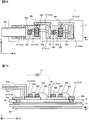
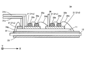
- FIG. 1 is a schematic diagram illustrating a configuration example of a power semiconductor module according to the present embodiment.
- FIG. 1A is a schematic plan view seen from the element arrangement surface side
- FIG. 1B is a schematic cross-sectional view showing a conductive wire.
- the power semiconductor module 1 includes a first ceramic substrate 11 serving as a support member.
- the first ceramic substrate 11 is a substrate having a substantially rectangular planar shape made of an insulating material such as silicon nitride, aluminum nitride, or aluminum oxide.
- a first conductive layer 21 made of a plurality of metal plates is provided on one main surface (upper side) which is the element arrangement surface side of the first ceramic substrate 11, and the other main surface of the first ceramic substrate 11.
- a second conductive layer 22 made of a metal plate is provided on the lower side.
- the metal plates constituting the first conductive layer 21 and the second conductive layer 22 are made of a metal material such as copper or aluminum and are brazed to the first ceramic substrate 11.
- the first conductive layer 21 may be a conductive member made of a conductive material other than metal.
- the first conductive layer 21 is composed of metal plates 21a to 21f that are spaced apart from each other.
- An external connection terminal 31a for power supply is connected to the metal plate 21a
- an external connection terminal 31b for power supply is connected to the metal plate 21b
- an output terminal 36 is connected to the metal plate 21c.
- the second conductive layer 22 is composed of a single metal plate.
- a diode 32a as a rectifying element and a transistor 33a as a switching element are arranged on the metal plate 21b. Terminals are formed on the lower surfaces of the diode 32a and the transistor 33a so as to be exposed, and the terminals and the metal plate 21b are electrically connected by solder. Further, terminals are respectively formed on the upper surfaces of the diode 32a and the transistor 33a, and conductive wires 34a to 34c are connected to the terminals so as to form a connection relationship described later.
- a diode 32b as a rectifying element and a transistor 33b as a switching element are arranged on the metal plate 21c. Terminals are respectively formed on the lower surfaces of the diode 32b and the transistor 33b so that the terminals are electrically connected to the metal plate 21c by soldering. In addition, terminals are formed on the upper surfaces of the diode 32b and the transistor 33b so that the terminals are exposed, and conductive wires 34d to 34f are connected to the terminals so as to form a connection relationship described later.
- the transistors 33a and 33b and the diodes 32a and 32b described above are made of a semiconductor material having a wider band gap than silicon. Since the transistors 33a and 33b and the diodes 32a and 32b made of such a semiconductor material can have lower on-resistance than transistors made of silicon, conduction loss can be reduced. Further, the transistors 33a and 33b and the diodes 32a and 32b made of such a semiconductor material can operate at a relatively high temperature of 200 ° C. or higher. As such a wide band gap semiconductor material, for example, silicon carbide (SiC) or gallium nitride (GaN) can be used.
- SiC silicon carbide
- GaN gallium nitride
- the transistors 33a and 33b are preferably, for example, FETs. By using FETs as the transistors 33a and 33b, the switching speed can be increased, and the conversion efficiency of the power converter when the power semiconductor module 1 is used can be increased. However, the transistors 33a and 33b are not limited to FETs.
- a second ceramic substrate 12 having substantially the same shape as the first ceramic substrate 11 is provided on the lower surface of the second conductive layer 22.
- the second ceramic substrate 12 is made of silicon nitride, aluminum nitride, aluminum oxide, or the like so that the lower surface of the second conductive layer 22 and the upper surface of the second ceramic substrate 12 are in contact with each other.
- the entire lower surface of the second conductive layer 22 is brazed.
- a third conductive layer 23 made of a metal plate is provided on the lower surface of the second ceramic substrate 12.
- the third conductive layer 23 is made of a metal material such as copper or aluminum, and is soldered to the second ceramic substrate 12 so that the lower surface of the second ceramic substrate 12 and the upper surface of the third conductive layer 23 are in contact with each other. ing.
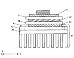
- FIG. 2 is a view of the power semiconductor module with the heat dissipation member attached as viewed from the direction of the arrow X1 shown in FIGS. 1A and 1B. However, in FIG. 2, a part of the configuration of the power semiconductor module is omitted.
- a copper base 42 of the heat dissipation member 41 is soldered to the lower surface of the third conductive layer 23.
- the cooling fins 44 are fixed to the copper base 42 by bolts 43 screwed from the upper surface of the copper base 42 in a state where the lower surface of the copper base 42 and the upper surface of the cooling fin 44 are in contact with each other. Thereby, the power semiconductor module 1 can be kept in an operable temperature range.
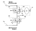
- FIG. 3 is a circuit configuration diagram of the power semiconductor module according to the present embodiment.
- a transistor 33a that is an n-channel FET and a transistor 33b that is an n-channel FET are provided in the power semiconductor module 1, between the external connection terminal 31a for power supply and the external connection terminal 31b.
- a transistor 33a that is an n-channel FET and a transistor 33b that is an n-channel FET are provided in the power semiconductor module 1, between the external connection terminal 31a for power supply and the external connection terminal 31b.
- a transistor 33a that is an n-channel FET and a transistor 33b that is an n-channel FET are provided in series.
- the drain terminal exposed on the lower surface of the transistor 33a is connected to the metal plate 21b, and a high potential from the power source is applied through the external connection terminal 31b.
- the source terminal exposed on the upper surface of the transistor 33b is connected to the metal plate 21d by a conductive wire 34e. Further, the metal plate 21 d is electrically connected to the metal plate constituting the second conductive layer 22 by the connection member 35 b provided in the through hole of the first ceramic substrate 11, and constitutes the second conductive layer 22. The metal plate is electrically connected to the metal plate 21 a by a connection member 35 a provided in the through hole of the first ceramic substrate 11. Thereby, a low potential is applied to the source terminal of the transistor 33b through the external connection terminal 31a.
- the source terminal exposed on the upper surface of the transistor 33a is connected to the metal plate 21c by the conductive wire 34b.
- the drain terminal exposed on the lower surface of the transistor 33b is connected to the metal plate 21c. Thereby, the source terminal of the transistor 33a and the drain terminal of the transistor 33b are connected to the common output terminal 36 connected to the metal plate 21c.
- the gate terminal exposed on the upper surface of the transistor 33a is connected to the metal plate 21e by the conductive wire 34c, and a control potential for controlling the switching of the transistor 33a is applied from the outside through the metal plate 21e and the conductive wire 34c. It is like that.
- the gate terminal exposed on the upper surface of the transistor 33b is connected to the metal plate 21f by the conductive wire 34f, and a control potential for controlling the switching of the transistor 33b is applied from the outside through the metal plate 21f and the conductive wire 34f. It has come to be.
- the transistors 33a and 33b are n-channel FETs, they are turned on when the potential difference generated between the gate and the source is larger than the threshold voltage, and turned off when the potential difference generated between the gate and the source is smaller than the threshold voltage. It becomes.
- a diode 32a is connected in parallel to the transistor 33a. Specifically, the cathode exposed on the lower surface of the diode 32a is connected to the metal plate 21b, and the anode exposed on the upper surface of the diode 32a is connected to the drain terminal exposed on the upper surface of the transistor 33a by the conductive wire 34a. Has been. Thereby, the reverse bias is applied to the diode 32a from the power source.
- a diode 32b is connected in parallel to the transistor 33b. Specifically, the cathode exposed on the lower surface of the diode 32b is connected to the metal plate 21c, and the anode exposed on the upper surface of the diode 32b is connected to the drain terminal exposed on the upper surface of the transistor 33b by the conductive wire 34d. Has been. Thereby, the reverse bias is applied to the diode 32b from the power source.
- a predetermined high potential is applied to the gate of the transistor 33a to turn on the transistor 33a, or a predetermined high potential is applied to the gate of the transistor 33b to cause the transistor 33b.
- a predetermined high potential is applied to the gate of the transistor 33a to turn on the transistor 33a
- a predetermined high potential is applied to the gate of the transistor 33b to cause the transistor 33b.
- it is possible to control the voltage appearing at the output terminal 36 according to whether the transistors 33a and 33b are on or off.
- it is used as an inverter that converts direct current into alternating current (single-phase alternating current when there are two power semiconductor modules 1 and three-phase alternating current when there are two). Can do.
- the temperature of each part of the power semiconductor module is simulated when using conventional silicon (Si) and when using silicon carbide (SiC) for the transistor. did.
- a simulation was performed for two conditions of an element A1 using silicon carbide (SiC) and an element A2 using silicon (Si).
- simulation was performed on two conditions of the structure B1 having the second ceramic substrate and the third conductive layer, and the structure B2 having no second conductive substrate.
- ⁇ T (j ⁇ c) represents a temperature difference from the contact surface between the transistor and the metal plate in the semiconductor module to the contact surface between the heat dissipation member and the semiconductor module
- ⁇ T (c ⁇ a) represents the temperature difference in the heat dissipation member.
- the temperature difference from the contact surface with the semiconductor module to the atmosphere is shown.
- the atmospheric temperature was 40 ° C.
- a second ceramic substrate that is thermally disadvantageous is provided to prevent charging of the heat dissipation member, but a structure that does not include the second ceramic substrate (Comparative 1).
- the change in Rth (ca) remains at about 5%.
- the power semiconductor module 1 according to the present embodiment has a large heat dissipation member despite the thermally disadvantageous two-layer substrate structure (two-layer structure of the first ceramic substrate and the second ceramic substrate). It is not necessary to use a thermal design, and it is not necessary to change the thermal design greatly.
- the power semiconductor module 1 has a thermal margin in spite of adopting a thermally disadvantageous two-layer substrate structure to prevent the heat radiation member from being charged. It can operate sufficiently without using a large heat dissipation member.
- the power semiconductor module using silicon since the power semiconductor module using silicon has no thermal margin, if the two-layer substrate structure is adopted, the heat dissipation member must be enlarged.
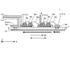
- FIG. 5 is a schematic diagram showing the direction of current change of the power semiconductor module according to the present embodiment.
- the metal plate 21 a provided on the upper surface of the first ceramic substrate 11 is provided on the lower surface of the first ceramic substrate 11 by the connection member 35 a provided in the through hole of the first ceramic substrate 11.
- Two conductive layers 22 are connected.
- the metal plate 21 d provided on the upper surface of the first ceramic substrate 11 is connected to the second conductive layer 22 by a connection member 35 b provided in the through hole of the first ceramic substrate 11.
- the external connection terminal 31b, the metal plate 21b, the metal plate 21c, and the metal plate 21d on the upper surface of the first ceramic substrate 11 are connected to the second conductive layer 22 on the lower surface of the first ceramic substrate 11 by the connection member 35b.
- the second conductive layer 22 on the lower surface of the first ceramic substrate 11 and the metal plate 21a and the external connection terminal 31a on the upper surface of the first ceramic substrate 11 are connected by the connection member 35a to form a circuit. .
- the metal plate constituting the second conductive layer 22 Since the change of the current transmitted to the second conductive layer 22 is transmitted to the low potential external connection terminal 31a through the connection member 35a and the conductive member 21a, the metal plate constituting the second conductive layer 22 is directed leftward (arrow X3). Change in current (increase in current) occurs. In other words, the switching of the transistor 33b causes reverse current changes in the metal plates 21b and 21c constituting the first conductive layer 21 and the second conductive layer 22 opposed thereto. More specifically, a reverse current change occurs in the opposing region of the metal plate 21b and the second conductive layer 22, and a reverse current change occurs in the opposing region of the metal plate 21c and the second conductive layer 22.
- the current change in the reverse direction is performed between the metal plates 21 b and 21 c constituting the first conductive layer 21 and the metal plate constituting the second conductive layer 22. Is configured to occur. For this reason, the inductive reactance (inductance) of the circuit is reduced by the mutual inductance between the metal plates 21 b and 21 c constituting the first conductive layer 21 and the metal plate constituting the second conductive layer 22. For example, in the power semiconductor module 1 according to the present embodiment, it has been confirmed that the inductance of the circuit can be reduced to about 1/10. Thus, the surge voltage in the power semiconductor module 1 can be suppressed by reducing the inductance of the circuit. Note that the direction of the current change in the metal plates 21b and 21c and the direction of the current change in the metal plate constituting the second conductive layer 22 need not be opposite to 180 ° if the circuit inductance can be reduced. good.
- the surge voltage generated in the above circuit increases as the switching speed increases. This is because the surge voltage depends on the product of the inductive reactance and the time derivative (di / dt) of the current.
- the transistors 33a and 33b are FETs, the switching speed increases, so that the time differentiation of the current at the time of switching increases.
- the reverse current flows in the opposing regions.
- the third conductive layer 23 is insulated from the first conductive layer 21 and the second conductive layer 22 by the second ceramic substrate 12. Thereby, the conduction
- Such electric shock prevention measures are particularly effective in fields where safety is important, such as railway vehicles and automobiles.
- the third conductive layer 23 is preferably connected to the ground.
- the anode exposed on the upper surface of the diode 32a and the metal plate 21c are connected to the source terminal exposed on the upper surface of the transistor 33a.
- the anode exposed on the upper surface of the diode 32b and the metal plate 21d are connected to the source terminal exposed on the upper surface of the transistor 33b.
- the metal plate 21d when the anode of the diode 32b and the metal plate 21d are directly connected, the metal plate 21d includes a conductive wire that connects the source terminal of the transistor 33b and the metal plate 21d, and the anode of the diode 32b. Since a conductive wire that connects the metal plate 21d is connected, the metal plate 21d requires a certain area. On the other hand, in the configuration according to the present embodiment, since only the conductive wire that connects the source terminal of the transistor 33b and the metal plate 21d is connected to the metal plate 21d, the area of the metal plate 21d can be reduced. Thereby, it is possible to reduce the size of the power semiconductor module.
- FIG. 6 is a schematic diagram showing a modification of the power semiconductor module according to the present embodiment.
- the basic configuration of the power semiconductor module 1 a shown in FIG. 6 is the same as that of the power semiconductor module 1.
- the main differences between the power semiconductor module 1a according to the present embodiment and the power semiconductor module 1 are the size of the first ceramic substrate 11 and the structure of the connection portion between the first conductive layer 21 and the second conductive layer 22. It is.
- the first ceramic substrate 11 is slightly smaller than the second ceramic substrate 12, and the width in the horizontal direction (X direction) in the drawing is short. Thereby, part of the upper surface is exposed at both ends of the second conductive layer 22. Further, the conductive wire 34e connects the source terminal of the transistor 33b and the exposed portion at one end of the metal plate constituting the second conductive layer 22, and accordingly, the metal plate 21d is omitted. Has been. In addition, a portion exposed at the other end of the metal plate constituting the second conductive layer 22 and the metal plate 21a are connected by the conductive wire 34g. That is, in the present embodiment, the conductive wire 34e and the conductive wire 34g function as connection members. As described above, when the first conductive layer 21 and the second conductive layer 22 are electrically connected by wire bonding, it is not necessary to provide a through hole and a connection member in the first ceramic substrate, thereby simplifying the manufacturing process. Is possible.
- the same effect as that of the power semiconductor module 1 can be obtained in the power semiconductor module 1a having such a configuration.
- the configuration of the present invention by using a transistor formed of a material having a wider band gap than silicon, the on-resistance is reduced, and a desired operation is possible even at a high temperature.
- a power semiconductor module that can be operated without being used can be realized.
- the inductive reactance of the circuit can be reduced by the mutual inductance and the surge voltage can be suppressed. Thereby, it is possible to realize a power semiconductor module capable of fully utilizing the characteristics of the transistor and exhibiting high performance.
- the present invention is not limited to the above embodiment, and can be implemented with various modifications.
- an IGBT may be used as the transistor.
- the size, shape, and the like illustrated in the accompanying drawings are not limited thereto, and can be appropriately changed within a range in which the effect of the present invention is exhibited.
- various modifications can be made without departing from the scope of the object of the present invention.
Landscapes
- Engineering & Computer Science (AREA)
- Power Engineering (AREA)
- Microelectronics & Electronic Packaging (AREA)
- Physics & Mathematics (AREA)
- Condensed Matter Physics & Semiconductors (AREA)
- General Physics & Mathematics (AREA)
- Computer Hardware Design (AREA)
- Inverter Devices (AREA)
- Dc-Dc Converters (AREA)
Applications Claiming Priority (2)
| Application Number | Priority Date | Filing Date | Title |
|---|---|---|---|
| JP2011168469A JP2013033812A (ja) | 2011-08-01 | 2011-08-01 | パワー半導体モジュール |
| JP2011-168469 | 2011-08-01 |
Publications (1)
| Publication Number | Publication Date |
|---|---|
| WO2013018811A1 true WO2013018811A1 (ja) | 2013-02-07 |
Family
ID=47629332
Family Applications (1)
| Application Number | Title | Priority Date | Filing Date |
|---|---|---|---|
| PCT/JP2012/069512 Ceased WO2013018811A1 (ja) | 2011-08-01 | 2012-07-31 | パワー半導体モジュール |
Country Status (2)
| Country | Link |
|---|---|
| JP (1) | JP2013033812A (enExample) |
| WO (1) | WO2013018811A1 (enExample) |
Cited By (4)
| Publication number | Priority date | Publication date | Assignee | Title |
|---|---|---|---|---|
| WO2014091608A1 (ja) * | 2012-12-13 | 2014-06-19 | 株式会社 日立製作所 | パワー半導体モジュール及びこれを用いた電力変換装置 |
| WO2014184030A1 (de) * | 2013-05-14 | 2014-11-20 | Audi Ag | Vorrichtung und elektrische baugruppe zum wandeln einer gleichspannung in eine wechselspannung |
| CN110783323A (zh) * | 2019-09-10 | 2020-02-11 | 杭州泰昕微电子有限公司 | 一种应用于逆变焊机的大功率集成器件 |
| US10811329B2 (en) | 2015-02-17 | 2020-10-20 | Koninklijke Philips N.V. | Ceramic substrate and method for producing a ceramic substrate |
Families Citing this family (10)
| Publication number | Priority date | Publication date | Assignee | Title |
|---|---|---|---|---|
| JP5566354B2 (ja) * | 2011-09-06 | 2014-08-06 | 三菱電機株式会社 | 電力用半導体スイッチおよび電力変換装置 |
| JP6331543B2 (ja) * | 2014-03-24 | 2018-05-30 | 日産自動車株式会社 | ハーフブリッジパワー半導体モジュール及びその製造方法 |
| EP3166144B1 (en) * | 2014-07-03 | 2019-08-07 | Nissan Motor Co., Ltd | Half-bridge power semiconductor module and manufacturing method therefor |
| WO2016084241A1 (ja) | 2014-11-28 | 2016-06-02 | 日産自動車株式会社 | ハーフブリッジパワー半導体モジュール及びその製造方法 |
| WO2017002390A1 (ja) * | 2015-06-30 | 2017-01-05 | シャープ株式会社 | 回路モジュール |
| JP6468984B2 (ja) | 2015-10-22 | 2019-02-13 | 三菱電機株式会社 | 半導体装置 |
| WO2017090281A1 (ja) * | 2015-11-25 | 2017-06-01 | シャープ株式会社 | モジュール基板 |
| EP3442020B1 (en) * | 2016-03-24 | 2020-10-07 | Hitachi, Ltd. | Power semiconductor module |
| JP7337711B2 (ja) * | 2020-01-09 | 2023-09-04 | 三菱電機株式会社 | 半導体装置 |
| JP2025042424A (ja) * | 2023-09-14 | 2025-03-27 | 株式会社東芝 | 半導体装置 |
Citations (4)
| Publication number | Priority date | Publication date | Assignee | Title |
|---|---|---|---|---|
| JP2002373971A (ja) * | 2001-03-30 | 2002-12-26 | Hitachi Ltd | 半導体装置 |
| JP2003168777A (ja) * | 2001-11-30 | 2003-06-13 | Kyocera Corp | インバータ制御モジュール |
| JP2009182261A (ja) * | 2008-01-31 | 2009-08-13 | Rohm Co Ltd | 半導体装置 |
| JP2011142172A (ja) * | 2010-01-06 | 2011-07-21 | Mitsubishi Electric Corp | 電力用半導体装置 |
-
2011
- 2011-08-01 JP JP2011168469A patent/JP2013033812A/ja not_active Withdrawn
-
2012
- 2012-07-31 WO PCT/JP2012/069512 patent/WO2013018811A1/ja not_active Ceased
Patent Citations (4)
| Publication number | Priority date | Publication date | Assignee | Title |
|---|---|---|---|---|
| JP2002373971A (ja) * | 2001-03-30 | 2002-12-26 | Hitachi Ltd | 半導体装置 |
| JP2003168777A (ja) * | 2001-11-30 | 2003-06-13 | Kyocera Corp | インバータ制御モジュール |
| JP2009182261A (ja) * | 2008-01-31 | 2009-08-13 | Rohm Co Ltd | 半導体装置 |
| JP2011142172A (ja) * | 2010-01-06 | 2011-07-21 | Mitsubishi Electric Corp | 電力用半導体装置 |
Cited By (5)
| Publication number | Priority date | Publication date | Assignee | Title |
|---|---|---|---|---|
| WO2014091608A1 (ja) * | 2012-12-13 | 2014-06-19 | 株式会社 日立製作所 | パワー半導体モジュール及びこれを用いた電力変換装置 |
| WO2014184030A1 (de) * | 2013-05-14 | 2014-11-20 | Audi Ag | Vorrichtung und elektrische baugruppe zum wandeln einer gleichspannung in eine wechselspannung |
| US9742312B2 (en) | 2013-05-14 | 2017-08-22 | Audi Ag | Apparatus and electrical assembly for converting a direct voltage into an alternating voltage |
| US10811329B2 (en) | 2015-02-17 | 2020-10-20 | Koninklijke Philips N.V. | Ceramic substrate and method for producing a ceramic substrate |
| CN110783323A (zh) * | 2019-09-10 | 2020-02-11 | 杭州泰昕微电子有限公司 | 一种应用于逆变焊机的大功率集成器件 |
Also Published As
| Publication number | Publication date |
|---|---|
| JP2013033812A (ja) | 2013-02-14 |
Similar Documents
| Publication | Publication Date | Title |
|---|---|---|
| WO2013018811A1 (ja) | パワー半導体モジュール | |
| JP6513303B2 (ja) | 電力用半導体モジュールおよび電力変換装置 | |
| US8987777B2 (en) | Stacked half-bridge power module | |
| US10756057B2 (en) | Half-bridge power semiconductor module and method of manufacturing same | |
| WO2013027819A1 (ja) | 半導体モジュール | |
| WO2016002385A1 (ja) | ハーフブリッジパワー半導体モジュール及びその製造方法 | |
| US20190318999A1 (en) | Semiconductor device | |
| US9812411B2 (en) | Semiconductor device, inverter circuit, and drive device | |
| US10855196B2 (en) | Semiconductor device | |
| WO2020174741A1 (ja) | 半導体装置 | |
| US20220263425A1 (en) | Electric circuit device | |
| US12334427B2 (en) | Semiconductor device | |
| US11973064B2 (en) | Semiconductor power module | |
| US20230197581A1 (en) | Power semiconductor module and method of manufacturing the same | |
| JP2021141221A (ja) | 半導体モジュール | |
| JP6763246B2 (ja) | 半導体装置 | |
| JP2014072385A (ja) | 半導体装置 | |
| JP5925328B2 (ja) | パワー半導体モジュール | |
| JP6665804B2 (ja) | 半導体装置 | |
| JP2017093232A (ja) | パワー半導体モジュールおよび電力変換装置 | |
| US20240282662A1 (en) | Power module | |
| KR102413991B1 (ko) | Pcb 일체형 고속 스위칭 전력변환 장치 | |
| JP7421259B2 (ja) | 電力変換装置 | |
| US20250096069A1 (en) | Power module and method of fabricating the same | |
| US11276627B2 (en) | Semiconductor device |
Legal Events
| Date | Code | Title | Description |
|---|---|---|---|
| 121 | Ep: the epo has been informed by wipo that ep was designated in this application |
Ref document number: 12820678 Country of ref document: EP Kind code of ref document: A1 |
|
| NENP | Non-entry into the national phase |
Ref country code: DE |
|
| 122 | Ep: pct application non-entry in european phase |
Ref document number: 12820678 Country of ref document: EP Kind code of ref document: A1 |