WO2013018287A1 - 光起電力装置 - Google Patents
光起電力装置 Download PDFInfo
- Publication number
- WO2013018287A1 WO2013018287A1 PCT/JP2012/004485 JP2012004485W WO2013018287A1 WO 2013018287 A1 WO2013018287 A1 WO 2013018287A1 JP 2012004485 W JP2012004485 W JP 2012004485W WO 2013018287 A1 WO2013018287 A1 WO 2013018287A1
- Authority
- WO
- WIPO (PCT)
- Prior art keywords
- glass substrate
- antireflection layer
- light
- photovoltaic device
- layer
- Prior art date
- Legal status (The legal status is an assumption and is not a legal conclusion. Google has not performed a legal analysis and makes no representation as to the accuracy of the status listed.)
- Ceased
Links
Images

Classifications
-
- H—ELECTRICITY
- H10—SEMICONDUCTOR DEVICES; ELECTRIC SOLID-STATE DEVICES NOT OTHERWISE PROVIDED FOR
- H10F—INORGANIC SEMICONDUCTOR DEVICES SENSITIVE TO INFRARED RADIATION, LIGHT, ELECTROMAGNETIC RADIATION OF SHORTER WAVELENGTH OR CORPUSCULAR RADIATION
- H10F10/00—Individual photovoltaic cells, e.g. solar cells
- H10F10/10—Individual photovoltaic cells, e.g. solar cells having potential barriers
- H10F10/17—Photovoltaic cells having only PIN junction potential barriers
- H10F10/172—Photovoltaic cells having only PIN junction potential barriers comprising multiple PIN junctions, e.g. tandem cells
-
- H—ELECTRICITY
- H10—SEMICONDUCTOR DEVICES; ELECTRIC SOLID-STATE DEVICES NOT OTHERWISE PROVIDED FOR
- H10F—INORGANIC SEMICONDUCTOR DEVICES SENSITIVE TO INFRARED RADIATION, LIGHT, ELECTROMAGNETIC RADIATION OF SHORTER WAVELENGTH OR CORPUSCULAR RADIATION
- H10F10/00—Individual photovoltaic cells, e.g. solar cells
- H10F10/10—Individual photovoltaic cells, e.g. solar cells having potential barriers
- H10F10/14—Photovoltaic cells having only PN homojunction potential barriers
- H10F10/146—Back-junction photovoltaic cells, e.g. having interdigitated base-emitter regions on the back side
-
- H—ELECTRICITY
- H10—SEMICONDUCTOR DEVICES; ELECTRIC SOLID-STATE DEVICES NOT OTHERWISE PROVIDED FOR
- H10F—INORGANIC SEMICONDUCTOR DEVICES SENSITIVE TO INFRARED RADIATION, LIGHT, ELECTROMAGNETIC RADIATION OF SHORTER WAVELENGTH OR CORPUSCULAR RADIATION
- H10F19/00—Integrated devices, or assemblies of multiple devices, comprising at least one photovoltaic cell covered by group H10F10/00, e.g. photovoltaic modules
- H10F19/40—Integrated devices, or assemblies of multiple devices, comprising at least one photovoltaic cell covered by group H10F10/00, e.g. photovoltaic modules comprising photovoltaic cells in a mechanically stacked configuration
-
- H—ELECTRICITY
- H10—SEMICONDUCTOR DEVICES; ELECTRIC SOLID-STATE DEVICES NOT OTHERWISE PROVIDED FOR
- H10F—INORGANIC SEMICONDUCTOR DEVICES SENSITIVE TO INFRARED RADIATION, LIGHT, ELECTROMAGNETIC RADIATION OF SHORTER WAVELENGTH OR CORPUSCULAR RADIATION
- H10F77/00—Constructional details of devices covered by this subclass
- H10F77/30—Coatings
- H10F77/306—Coatings for devices having potential barriers
- H10F77/311—Coatings for devices having potential barriers for photovoltaic cells
- H10F77/315—Coatings for devices having potential barriers for photovoltaic cells the coatings being antireflective or having enhancing optical properties
-
- Y—GENERAL TAGGING OF NEW TECHNOLOGICAL DEVELOPMENTS; GENERAL TAGGING OF CROSS-SECTIONAL TECHNOLOGIES SPANNING OVER SEVERAL SECTIONS OF THE IPC; TECHNICAL SUBJECTS COVERED BY FORMER USPC CROSS-REFERENCE ART COLLECTIONS [XRACs] AND DIGESTS
- Y02—TECHNOLOGIES OR APPLICATIONS FOR MITIGATION OR ADAPTATION AGAINST CLIMATE CHANGE
- Y02E—REDUCTION OF GREENHOUSE GAS [GHG] EMISSIONS, RELATED TO ENERGY GENERATION, TRANSMISSION OR DISTRIBUTION
- Y02E10/00—Energy generation through renewable energy sources
- Y02E10/50—Photovoltaic [PV] energy
- Y02E10/547—Monocrystalline silicon PV cells
-
- Y—GENERAL TAGGING OF NEW TECHNOLOGICAL DEVELOPMENTS; GENERAL TAGGING OF CROSS-SECTIONAL TECHNOLOGIES SPANNING OVER SEVERAL SECTIONS OF THE IPC; TECHNICAL SUBJECTS COVERED BY FORMER USPC CROSS-REFERENCE ART COLLECTIONS [XRACs] AND DIGESTS
- Y02—TECHNOLOGIES OR APPLICATIONS FOR MITIGATION OR ADAPTATION AGAINST CLIMATE CHANGE
- Y02E—REDUCTION OF GREENHOUSE GAS [GHG] EMISSIONS, RELATED TO ENERGY GENERATION, TRANSMISSION OR DISTRIBUTION
- Y02E10/00—Energy generation through renewable energy sources
- Y02E10/50—Photovoltaic [PV] energy
- Y02E10/548—Amorphous silicon PV cells
Definitions
- the present invention relates to a photovoltaic device.
- the conventional antireflection film has room for further improvement in the compatibility between the adhesion to the glass substrate and the antireflection effect.
- the present invention has been made in view of such circumstances, and an object of the present invention is to provide a photovoltaic device capable of achieving both a light reflection preventing effect and reliability at a high level.
- a photovoltaic device is provided with a glass substrate, an antireflection layer formed on the light receiving surface side of the glass substrate, and a side opposite to the light receiving surface of the glass substrate. And a photovoltaic device that converts light into electricity.
- the antireflection layer is configured to have a refractive index smaller than that of the glass substrate, and the glass substrate has irregularities having a root mean square roughness RMS of 100 to 1100 nm on the light receiving surface side.
- both the antireflection effect of light and the reliability can be achieved at a high level.
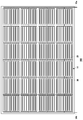
- FIG. 6 is a top view of a solar cell module according to Example 2.
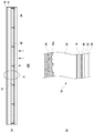
- FIG. 6A is a cross-sectional view of the solar cell module according to Example 2, and
- FIG. 6B is an enlarged view of a region A in FIG. 6A.
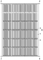
- 6 is a top view of a solar cell module according to Example 3.
- FIG. 8A is a cross-sectional view of the solar cell module according to Example 3, and
- FIG. 8B is an enlarged view of a region B in FIG. 8A.
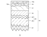
- FIG. 1 is a schematic sectional view of a photovoltaic device according to the present embodiment.
- the photovoltaic device 10 according to the present embodiment is provided on the opposite side of the glass substrate 12, the antireflection layer 14 formed on the light receiving surface 12a side of the glass substrate 12, and the light receiving surface 12a of the glass substrate 12.
- a photovoltaic element 16 for converting light into electricity is provided on the opposite side of the glass substrate 12, the antireflection layer 14 formed on the light receiving surface 12a side of the glass substrate 12, and the light receiving surface 12a of the glass substrate 12.
- a photovoltaic element 16 for converting light into electricity.
- the photovoltaic element 16 has a first electrode layer 18, a semiconductor layer 20, and a second electrode layer 22.
- the 1st electrode layer 18 is formed on the surface of the glass substrate 12, and has electroconductivity and translucency.
- a transparent conductive oxide film (TCO) is used, and in particular, zinc oxide (ZnO) having high light transmittance, low resistance, and low price is used. Is preferred.
- the semiconductor layer 20 generates charges (electrons and holes) by incident light from the first electrode layer 18 side.
- the semiconductor layer 20 for example, an amorphous (amorphous) silicon semiconductor layer having a pin junction or a pn junction as a basic structure, or a single layer or a stacked body of a microcrystalline silicon semiconductor layer can be used.
- the semiconductor layer 20 according to the present embodiment is configured by laminating an amorphous silicon semiconductor 24 and a microcrystalline silicon semiconductor 26 from the first electrode layer 18 side, respectively.
- the term “microcrystal” means not only a complete crystal state but also a state partially including an amorphous state.
- silicon oxide (SiO x ) having a thickness of about 30 nm may be provided as an intermediate layer between the amorphous silicon semiconductor 24 and the microcrystalline silicon semiconductor 26. Such an intermediate layer is formed by sputtering or the like.
- the second electrode layer 22 is formed on the microcrystalline silicon semiconductor 26.
- the second electrode layer 22 is made of a laminated structure of a transparent conductive oxide (TCO) such as zinc oxide (ZnO) and a reflective metal such as silver (Ag).
- TCO transparent conductive oxide
- ZnO zinc oxide
- Ag silver
- the second electrode layer 22 of one photovoltaic element 16 is disposed so as to be electrically connected to the first electrode layer 18 of another adjacent photovoltaic element 16. Thereby, one photovoltaic element 16 and the other photovoltaic element 16 are electrically connected in series.
- the antireflection layer 14 provided on the light receiving surface side of the photovoltaic device 10 has an intermediate refractive index between the refractive index (about 1.52) of the glass substrate 12 and the refractive index of the atmosphere (about 1.0). Things are desirable. However, since there are few solid materials that have a refractive index close to that of the atmosphere, silica-based inorganic materials or acrylic resin materials having a slightly lower refractive index than those of glass substrate materials have been used in the past. Since the rate was 1.46 or more, a sufficient antireflection effect was not obtained.
- the antireflective layer 14 according to the present embodiment has a refractive index of the material itself that is not so small as that of the glass substrate 12, it includes a large number of voids (holes 14a) inside as shown in FIG. ing. Thereby, since the average refractive index of the whole antireflection layer 14 becomes small, a higher antireflection effect can be exhibited.
- the antireflection layer 14 according to the present embodiment achieves a refractive index of 1.45, which is difficult only by selecting the material itself.
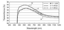
- FIG. 2 is a graph showing the relationship between the wavelength of light and the transmittance depending on the presence or absence of the antireflection layer and the difference in refractive index.
- line a and line c shown in FIG. 2 when the antireflection layer is uncoated or when the refractive index n of the antireflection layer is about 1.48, the wavelength range of visible light (about 400 to 1100 nm) The transmittance at is not sufficient.
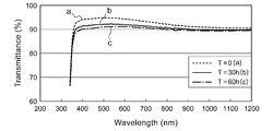
- FIG. 3 is a graph showing a change in the relationship between the wavelength of light and the transmittance by the pressure cooker test which is an accelerated deterioration test.
- the conditions of the pressure cooker test were a relative humidity of 99% rh, an internal pressure of 0.20 MPa, and an internal temperature of 121 ° C., the refractive index of the antireflection layer of the test piece was 1.45, and the surface of the glass substrate was smooth. Something is used.
- FIG. 3 it was found that with the passage of time in the pressure cooker test, the transmittance decreased in the entire wavelength range, and the antireflection effect decreased significantly. This is because the antireflection layer peeled off due to the penetration of moisture or the like into the antireflection layer or the interface between the glass substrate and the antireflection layer.
- the present inventor has conceived the following configuration.
- the antireflection layer 14 is configured to have a refractive index smaller than that of the glass substrate 12.
- the glass substrate 12 is provided with fine irregularities at the interface with the antireflection layer 14.
- the glass substrate 12 has irregularities in which the root mean square roughness RMS (Rq) measured by a method defined in JIS is in the range of 100 to 1100 nm.
- Rq root mean square roughness measured by a method defined in JIS
- the root mean square roughness RMS is less than 100 nm, the effect of improving the adhesion with the antireflection layer 14 is small.
- the root mean square roughness RMS is larger than 1100 nm, the size of the unevenness becomes larger than the wavelength of visible light. Therefore, the visible light in sunlight is geometrically reflected by the inclined uneven surface and reflected. Increases, the amount of transmitted light decreases.
- the glass substrate 12 may have irregularities with a root mean square roughness RMS of 400 nm or more. Thereby, adhesiveness with the antireflection layer 14 can further be improved.
- the measuring method of the root mean square roughness RMS first ultrasonically cleans the sample in which the antireflection layer is formed in an organic solvent (alcohol, acetone, etc.), and peels off the antireflection layer.
- the root mean square roughness RMS is calculated by measuring the exposed surface of the glass substrate with an atomic force microscope (AFM).
- the glass substrate 12 has irregularities at the interface with the antireflection layer 14, so that the glass substrate 12 and the antireflection layer 14 are in close contact with each other. And the reliability of the photovoltaic device 10 is increased. Further, the light is scattered by the irregularities on the surface of the glass substrate 12, so that the optical path length in the photovoltaic element 16 becomes long and the light is easily absorbed in the photovoltaic element 16.
- Example 1 Next, a manufacturing method of the photovoltaic device 10 according to the first embodiment will be described in detail.
- sandblasting abrasive material: WA # 1000, pressure: 0.2 MPa, injection amount: 34 g / s
- WA # 1000 abrasive material
- pressure: 0.2 MPa pressure: 0.2 MPa
- injection amount 34 g / s
- fine irregularities having a root mean square roughness RMS of 800 nm were formed on one main surface of the glass substrate 12.
- a liquid mainly composed of silica sol-gel is applied on the surface of the glass substrate 12 on which fine irregularities are formed, and baked at 150 ° C. for 30 minutes.
- An antireflection layer 14 having a thickness of 85 nm was obtained.
- the liquid mainly composed of silica sol-gel contains a surfactant, and the antireflection layer 14 is formed so as to include a large number of voids (holes 14a) by thermal decomposition of the surfactant
- the first electrode layer 18, the amorphous silicon semiconductor 24, the microcrystalline silicon semiconductor 26, and the second electrode layer 22 are sequentially stacked on the other main surface of the glass substrate 12 to form a tandem made of amorphous Si / microcrystalline Si.
- a structural cell was formed, and the photovoltaic device 10 according to Example 1 was fabricated.
- a tandem structure cell in which an antireflection layer equivalent to this embodiment was formed on a glass substrate on which fine unevenness was not formed was also produced.
- Table 1 shows the measurement results of the characteristics of the photovoltaic devices according to Example 1 and the comparative example. The measurement was performed a plurality of times, and the maximum value, minimum value, and average value are shown in Table 1.
- the items of measured values and calculated values shown in Table 1 are Voc (V): open circuit voltage, Isc (A): short circuit current, F.V. F. : Fill factor, Pmax: maximum power, ⁇ _cell (%): conversion efficiency.
- the photovoltaic device according to Example 1 was confirmed to improve by 2.67% with respect to the short circuit current (Isc) as compared with the photovoltaic device according to the comparative example. This is because the refractive index change at the interface between the antireflection layer and the glass substrate does not change stepwise with respect to visible light when sunlight proceeds to the atmosphere, the antireflection layer, or the glass substrate. It is considered that a larger antireflection effect was obtained as a result of a gradual change in the average refractive index due to unevenness.
- the photovoltaic device according to Example 1 was confirmed to have high reliability without any decrease in the short circuit current (Isc) with the passage of time even in the pressure cooker test.
- the antireflection layer 14 is a porous layer in which pores 14a are formed as described above. Thereby, the refractive index of the antireflection layer 14 can be appropriately reduced without changing the material.
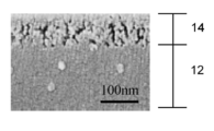
- FIG. 4 is a diagram showing a cross-sectional TEM photograph of an example of the antireflection layer.
- the antireflection layer shown in FIG. 4 has a pore size of about 100 nm ⁇ 10 nm and a porosity of about 10%.
- the average diameter of the holes varies depending on the measurement location, but can be regarded as a range of 10 to 100 nm.
- the pores may be formed such that the average diameter is smaller than the root mean square roughness RMS of the irregularities of the glass substrate.
- the proportion of the holes 14a may be reduced stepwise or continuously from the light receiving side toward the glass substrate side. Thereby, the reflectance in the antireflection layer 14 can be further lowered.
- the antireflection layer 14 may be configured such that the refractive index increases stepwise or continuously from the light receiving side toward the glass substrate side. Thereby, the reflectance in the antireflection layer 14 can be further lowered.
- the antireflection layer 14 is made of a material mainly composed of silicon dioxide having a density of 2.4 g / cm 3 or less, and may have a thickness in the range of 60 to 200 nm. Thereby, since the anti-reflective layer 14 is comprised with the material similar to the glass substrate 12, the adhesiveness of the glass substrate 12 and the anti-reflective layer 14 can be improved. Moreover, even if it is a case where the alkali metal is contained in the glass substrate 12 by the antireflection layer 14, precipitation of an alkali metal is suppressed and the cloudiness of the glass substrate 12 can be prevented.
- Example 2 Next, the solar cell module 100 according to Example 2 will be described. Below, description is abbreviate
- FIG. 1 is a diagrammatic representation of the solar cell module 100 according to Example 2.
- FIG. 5 is a top view of the solar cell module according to the second embodiment.
- 6A is a cross-sectional view of the solar cell module according to Example 2, and
- FIG. 6B is an enlarged view of a region A in FIG. 6A.
- the solar cell module shown in FIG. 5 is viewed from the back side opposite to the light receiving surface.
- a solar cell module 100 according to Example 2 includes a photovoltaic device 10, a wiring member 30, a filler 32, and a back member 34 as a protective member.
- the photovoltaic device 10 is provided on the opposite side of the glass substrate 12, the antireflection layer 14 formed on the light receiving surface 12a side of the glass substrate 12, and the light receiving surface 12a of the glass substrate 12, And a photovoltaic element 16 that converts light into electricity.
- a plurality of single-crystal Si solar cells as photovoltaic elements 16 are arranged in a matrix on one main surface of a glass substrate 12 as a support member, and these cells are bonded to the glass substrate 12. Is done. Further, the other main surface (sunlight incident surface) of the glass substrate 12 is uneven, and an anti-reflective coating 14 having a low refractive index is formed on the uneven surface.
- each solar cell has an IBC (Interdigitated Back Contact) in which comb-like positive and negative electrodes (Anode / Cathode) as wiring members 30 are provided only on the surface opposite to the light incident side. ) Has a structure. Each solar battery cell is connected in series and in parallel via a conductive member 36.
- IBC Interdigitated Back Contact
- EVA ethylene vinyl acetate copolymer
- the size of the unevenness provided on the sunlight incident side (light receiving surface 12a side) of the glass substrate 12 has a root mean square roughness RMS of 0.5 ⁇ m and is formed by sandblasting using aluminum oxide particles.
- the uneven reflection preventing layer 14 is a layer mainly composed of SiO 2 having a density of 2.2 g / cm 3 and a film thickness of 180 nm, and is a long wavelength light that causes a transmission loss of sunlight in a single crystal Si cell.
- the film thickness is suitable for suppressing reflection of (mainly light having a wavelength of 800 nm or more).
- the cell thickness is about 200 ⁇ m or more, and the light confinement effect is remarkably lowered when the cell thickness is reduced.
- a high light confinement effect was obtained even with single crystal Si having a thickness of 50 ⁇ m.
- the single crystal Si cell has a substantially square shape, and after forming an I (Intrinsic) type amorphous Si layer and a Si nitride layer as a passivation film on the light incident surface, the single crystal Si cell is bonded to the glass substrate 12 using an anodic bonding method.
- an anodic bonding method Has been.
- a fluorine-based resin or a glass frit can be used for bonding the single crystal Si cell and the glass substrate 12.
- the IBC structure which is the back surface structure of the single crystal Si cell is formed using photolithography. Then, the generated current is taken out through the anode electrode 30a and the cathode electrode 30b at both ends of the single crystal Si cell.
- Example 3 Next, the solar cell module 200 according to Example 3 will be described. In the following, the description of the same configuration as that of the above-described embodiment and each example will be omitted as appropriate.
- FIG. 7 is a top view of the solar cell module according to Example 3.
- FIG. 8A is a cross-sectional view of the solar cell module according to Example 3, and
- FIG. 8B is an enlarged view of a region B in FIG. 8A.
- the solar cell module shown in FIG. 7 is seen from the back side opposite to the light receiving surface.
- the solar cell module 200 according to Example 3 includes a single crystal Si solar cell that is the first photovoltaic element 16 as a bottom cell and an integrated amorphous Si solar cell that is the second photovoltaic element 17 as a top cell. And have. Single-crystal Si solar cells and integrated amorphous Si solar cells are arranged in two stages in parallel to the glass substrate 12 that is the light incident surface. Further, the integrated amorphous Si solar cell is disposed closer to the light incident surface than the single crystal Si solar cell.
- the integrated amorphous Si solar cell includes a step of sequentially forming a light-transmitting conductive oxide film (TCO), amorphous Si, and a light-transmitting conductive oxide film on a glass substrate 12, and a laser is applied to each of these stacked layers (films). And a step of forming an integrated structure by a patterning method.
- TCO light-transmitting conductive oxide film
- amorphous Si amorphous Si
- a light-transmitting conductive oxide film on a glass substrate 12
- a laser is applied to each of these stacked layers (films).
- a step of forming an integrated structure by a patterning method the size of the unevenness provided on the glass substrate 12 is 0.5 nm for the same RMS as in Example 2.
- the antireflection layer 14 is also required to prevent reflection of short wavelength light, it is 90 nm. Yes.
- the single crystal Si solar cell and the integrated amorphous Si solar cell are electrically completely insulated, and the generated power is taken out separately. Specifically, in the single crystal Si solar cell, the generated current is taken out through the anode electrode 30a and the cathode electrode 30b at both ends. On the other hand, in the integrated amorphous Si solar cell, the generated current is taken out through the anode electrode 31a and the cathode electrode 31b at both ends.
- the present invention has been described with reference to the above-described embodiment.
- the present invention is not limited to the above-described embodiment, and the present invention can be appropriately combined or replaced with the configuration of the embodiment. It is included in the present invention.
- the described embodiments can also be included in the scope of the present invention.
- the first electrode layer 18 in addition to zinc oxide (ZnO), tin oxide (SnO 2 ), indium oxide (In 2 O 3 ), titanium oxide (TiO 2 ), zinc stannate ( Zn 2 SnO 4) may be configured by a metal one kind selected from oxides or plural kinds of laminates such. Note that these metal oxides may be doped with fluorine (F), tin (Sn), aluminum (Al), gallium (Ga), niobium (Nb), or the like.
- F fluorine
- Sn tin
- Al aluminum
- Ga gallium
- Nb niobium
- the fine irregularities provided on the light receiving surface side of the glass substrate are formed by sandblasting, but may be formed by etching with hydrofluoric acid.
- the antireflection layer may be formed by applying a liquid material mainly composed of silicon particles having a predetermined particle size (particle size) onto a glass substrate and baking it.
- a gap generated between adjacent silicon particles corresponds to a gap as an antireflection layer.
- photovoltaic devices having the following combinations can also be included in the scope of the present invention.
- the photovoltaic device A glass substrate; An antireflection layer formed on the light receiving surface side of the glass substrate; A photovoltaic element provided on the side opposite to the light receiving surface of the glass substrate, which converts light into electricity,
- the antireflection layer is configured to have a refractive index smaller than that of the glass substrate,
- the glass substrate has irregularities having a root mean square roughness RMS of 100 to 1100 nm on the light receiving surface side.
- the root mean square roughness RMS When the root mean square roughness RMS is less than 100 nm, the effect of improving the adhesion with the antireflection layer 14 is small. On the other hand, when the root mean square roughness RMS is larger than 1100 nm, the size of the unevenness becomes larger than the wavelength of visible light. Therefore, the visible light in sunlight is geometrically reflected by the inclined uneven surface and reflected. Increases, the amount of transmitted light decreases.
- the porous layer is configured such that the ratio of the vacancies decreases stepwise or continuously from the light receiving side to the glass substrate side. It may be a photovoltaic device. Thereby, the reflectance in the antireflection layer can be further lowered.
- the antireflection layer is made of a material mainly composed of silicon dioxide having a density of 2.4 g / cm 3 or less, and has a thickness in the range of 60 to 200 nm (1) to (4) The photovoltaic device of any one of these may be sufficient.
- the antireflection layer is composed of a material having a composition similar to that of the glass substrate, adhesion between the glass substrate and the antireflection layer can be improved.
- an alkali metal is contained in the glass substrate by the antireflection layer, precipitation of the alkali metal is suppressed, and white turbidity of the glass substrate can be prevented.
- the present invention can be used for solar cells.
Landscapes
- Photovoltaic Devices (AREA)
Abstract
光起電力装置10は、ガラス基板12と、ガラス基板12の受光面側に形成されている反射防止層14と、ガラス基板の受光面と反対側に設けられ、光を電気に変える光起電力素子16と、を備える。反射防止層14は、ガラス基板12よりも屈折率が小さくなるように構成されており、ガラス基板12は、受光面側に、二乗平均平方根粗さRMSが100~1100nmの範囲の凹凸を有する。
Description
本発明は、光起電力装置に関する。
従来、光エネルギーを電気エネルギーに変換する光電変換装置として、いわゆる太陽電池の開発が各方面で精力的に行われている。太陽電池には、種々のタイプがあるが、近年、材料費の低減、低温プロセスによる製造の容易さ、などの観点から、薄膜シリコン太陽電池が注目されている。
通常、太陽電池では、半導体領域に吸収される光量が大きいほど、すなわち、光の強さを一定とすれば半導体領域内へ入射する光の量が多いほど、形成される電子および正孔の濃度が増し、変換効率が向上する。そのため、光が太陽電池の表面で反射してしまうと、それだけ半導体領域内に入射する光が減るため、変換効率の低下を招くことになる。そこで、太陽電池の表面に反射防止膜を設けた構成が知られている(例えば、特許文献1参照)。
しかしながら、従来の反射防止膜は、ガラス基板との密着性と、反射防止効果との両立において、更なる改善の余地がある。
本発明はこうした状況に鑑みてなされたものであり、その目的とするところは、光の反射防止効果と信頼性とを高いレベルで両立し得る光起電力装置を提供することにある。
上記課題を解決するために、本発明のある態様の光起電力装置は、ガラス基板と、ガラス基板の受光面側に形成されている反射防止層と、ガラス基板の受光面と反対側に設けられ、光を電気に変える光起電力素子と、を備える。反射防止層は、ガラス基板よりも屈折率が小さくなるように構成されており、ガラス基板は、受光面側に、二乗平均平方根粗さRMSが100~1100nmの範囲の凹凸を有する。
本発明によれば、光の反射防止効果と信頼性とを高いレベルで両立し得る。
以下、図面を参照しながら、本発明を実施するための形態について詳細に説明する。なお、図面の説明において同一の要素には同一の符号を付し、重複する説明を適宜省略する。
以下の各図に示す各層、各部の縮尺や形状は、説明を容易にするために便宜的に設定されており、特に言及がない限り限定的に解釈されるものではない。
図1は、本実施の形態に係る光起電力装置の概略断面図である。本実施の形態に係る光起電力装置10は、ガラス基板12と、ガラス基板12の受光面12a側に形成されている反射防止層14と、ガラス基板12の受光面12aと反対側に設けられ、光を電気に変える光起電力素子16と、を備える。
光起電力素子16は、第1電極層18、半導体層20および第2電極層22を有する。第1電極層18は、ガラス基板12の面上に形成されており、導電性および透光性を有する。本実施の形態に係る第1電極層18としては、透明導電性酸化膜(TCO)が用いられ、特に、高い光透過性、低抵抗性を有し、低価格である酸化亜鉛(ZnO)が好適である。
半導体層20は、第1電極層18側からの入射光により電荷(電子および正孔)を生成する。半導体層20としては、例えば、pin接合またはpn接合を基本構造として有するアモルファス(非晶質)シリコン半導体層や微結晶シリコン半導体層の単層体あるいは積層体を用いることができる。本実施の形態に係る半導体層20は、第1電極層18側からそれぞれアモルファスシリコン半導体24、微結晶シリコン半導体26が積層されたものとして構成されている。なお、本明細書において、「微結晶」の用語は、完全な結晶状態のみならず、部分的に非結晶状態を含む状態をも意味するものとする。
また、アモルファスシリコン半導体24と微結晶シリコン半導体26との間に、中間層として、膜厚30nm程度の酸化シリコン(SiOx)を設けてもよい。こうした中間層は、スパッタリング等により形成される。
第2電極層22は、微結晶シリコン半導体26上に形成される。第2電極層22は、酸化亜鉛(ZnO)などの透明導電性酸化物(TCO)と銀(Ag)などの反射性金属との積層構造体からなる。一の光起電力素子16の第2電極層22は、隣接する他の光起電力素子16の第1電極層18と導通するように配置されている。これにより、一の光起電力素子16と他の光起電力素子16とが電気的に直列に接続される。
次に、反射防止層について詳述する。反射防止層14に求められる特性は種々あるが、屈折率やガラス基板12との密着性が重要な特性である。光起電力装置10の受光面側に設けられる反射防止層14は、ガラス基板12の屈折率(約1.52)と、大気の屈折率(約1.0)との中間の屈折率を有するものが望ましい。しかし、大気に近い屈折率を有するような固体材料は少ないため、従来はガラス基板の材料よりもやや屈折率の小さなシリカ系無機材料、またはアクリル系樹脂材料などが用いられており、いずれも屈折率は1.46以上であることから、十分な反射防止効果が得られていなかった。
そこで、本実施の形態に係る反射防止層14は、材料自体の屈折率はガラス基板12よりもそれほど小さくはないが、図1に示すように内部に多くの空隙(空孔14a)を含ませている。これにより、反射防止層14全体の平均的な屈折率が小さくなるため、より高い反射防止効果を発揮できる。本実施の形態に係る反射防止層14は、材料自体の選択だけでは困難な屈折率1.45を実現している。
図2は、反射防止層の有無および屈折率の相違による光の波長と透過率との関係を示したグラフである。図2に示すラインaやラインcに示すように、反射防止層が未コートの場合や、反射防止層の屈折率nが1.48程度の場合、可視光の波長域(約400~1100nm)での透過率は十分なものとは言えない。一方、図2のラインbに示すように、ガラス基板12との屈折率の差が大きい反射防止層(屈折率n=1.45)を用いることで、可視光の波長域(約400~1100nm)での透過率が向上している。
一方、このような多くの空隙を含む反射防止層は、耐湿性、強度、および基板との密着性などが低下し、長期の屋外使用中に反射防止層がはく離、損傷することで、反射防止効果が低下する点に改善の余地がある。
図3は、加速劣化試験であるプレッシャークッカー試験による光の波長と透過率との関係の変化を示したグラフである。プレッシャークッカー試験の条件は、相対湿度99%rh、器内圧力0.20MPa、器内温度121℃、であり、試験片の反射防止層の屈折率は1.45、ガラス基板の表面は平滑なものを用いている。図3に示すように、プレッシャークッカー試験の時間の経過とともに、透過率が全波長域で低下しており、反射防止効果が著しく低下することが判明した。これは、反射防止層の内部や、ガラス基板と反射防止層との界面への水分等の浸透により、反射防止層がはく離したことが原因である。
そこで、本発明者は、反射防止層の屈折率を小さくしつつ、反射防止層とガラス基板との密着性を向上するために鋭意検討した結果、以下の構成に想到した。
前述のように、本実施の形態に係る反射防止層14は、ガラス基板12よりも屈折率が小さくなるように構成されている。加えて、ガラス基板12は、反射防止層14との界面において、微細な凹凸が設けられている。具体的には、ガラス基板12は、JISで規定されている方法によって測定された二乗平均平方根粗さRMS(Rq)が100~1100nmの範囲の凹凸を有する。二乗平均平方根粗さRMSが100nm未満であると、反射防止層14との密着性の改善の効果が小さい。一方、二乗平均平方根粗さRMSが1100nmより大きいと、凹凸の大きさが可視光の波長よりも大きくなってしまうため、太陽光中の可視光は、傾斜した凹凸面で幾何学反射し反射率が高まるため、透過光量が減少する。
なお、400nm以下の波長の光は、ガラス基板12で吸収されやすく、光起電力素子16での発電に寄与する割合は高くない。そこで、ガラス基板12は、二乗平均平方根粗さRMSが400nm以上の範囲の凹凸を有してもよい。これにより、反射防止層14との密着性を更に向上できる。
なお、二乗平均平方根粗さRMSの測定方法は、はじめに反射防止層の形成された試料を有機溶剤中(アルコール,アセトンなど)で超音波洗浄し、反射防止層をはく離する。次に、露出したガラス基板の表面を原子間力顕微鏡(AFM)により測定することにより二乗平均平方根粗さRMSを算出する。
このように、本実施の形態に係る光起電力装置10においては、ガラス基板12は、反射防止層14との界面において凹凸を有しているため、ガラス基板12と反射防止層14との密着性が増し、光起電力装置10の信頼性が増す。また、ガラス基板12表面の凹凸により、光が散乱することで、光起電力素子16での光路長が長くなり、光起電力素子16において光が吸収されやすくなる。
(実施例1)
次に、実施例1に係る光起電力装置10の製造方法について詳述する。はじめに、ガラス基板12の一方の主面にサンドブラスト(研磨材:WA#1000、圧力:0.2MPa、噴射量:34g/s)処理を行った。その結果、ガラス基板12の一方の主面に二乗平均平方根粗さRMSが800nmの微細な凹凸が形成された。そして、ガラス基板12の、微細な凹凸が形成されている側の面上に、シリカゾルゲルを主成分とする液体を塗布し、150℃で30分間焼成することにより、屈折率1.45、膜厚85nmの反射防止層14を得た。シリカゾルゲルを主成分とする液体は、界面活性剤を含み、この界面活性剤の熱分解により、反射防止層14は多数の空隙(空孔14a)を含むように形成される。
次に、実施例1に係る光起電力装置10の製造方法について詳述する。はじめに、ガラス基板12の一方の主面にサンドブラスト(研磨材:WA#1000、圧力:0.2MPa、噴射量:34g/s)処理を行った。その結果、ガラス基板12の一方の主面に二乗平均平方根粗さRMSが800nmの微細な凹凸が形成された。そして、ガラス基板12の、微細な凹凸が形成されている側の面上に、シリカゾルゲルを主成分とする液体を塗布し、150℃で30分間焼成することにより、屈折率1.45、膜厚85nmの反射防止層14を得た。シリカゾルゲルを主成分とする液体は、界面活性剤を含み、この界面活性剤の熱分解により、反射防止層14は多数の空隙(空孔14a)を含むように形成される。
次に、ガラス基板12の他方の主面上に、第1電極層18、アモルファスシリコン半導体24、微結晶シリコン半導体26、第2電極層22を順次積層し、アモルファスSi/微結晶Siからなるタンデム構造セルを形成し、実施例1に係る光起電力装置10を作製した。
一方、比較例に係る光起電力装置として、微細凹凸が形成されていないガラス基板上に、本実施の形態と同等の反射防止層を形成したタンデム構造セルも作製した。表1は、実施例1および比較例に係る光起電力装置の特性の測定結果を示している。なお、測定は複数回行い、最大値、最小値、平均値を表1に記載している。
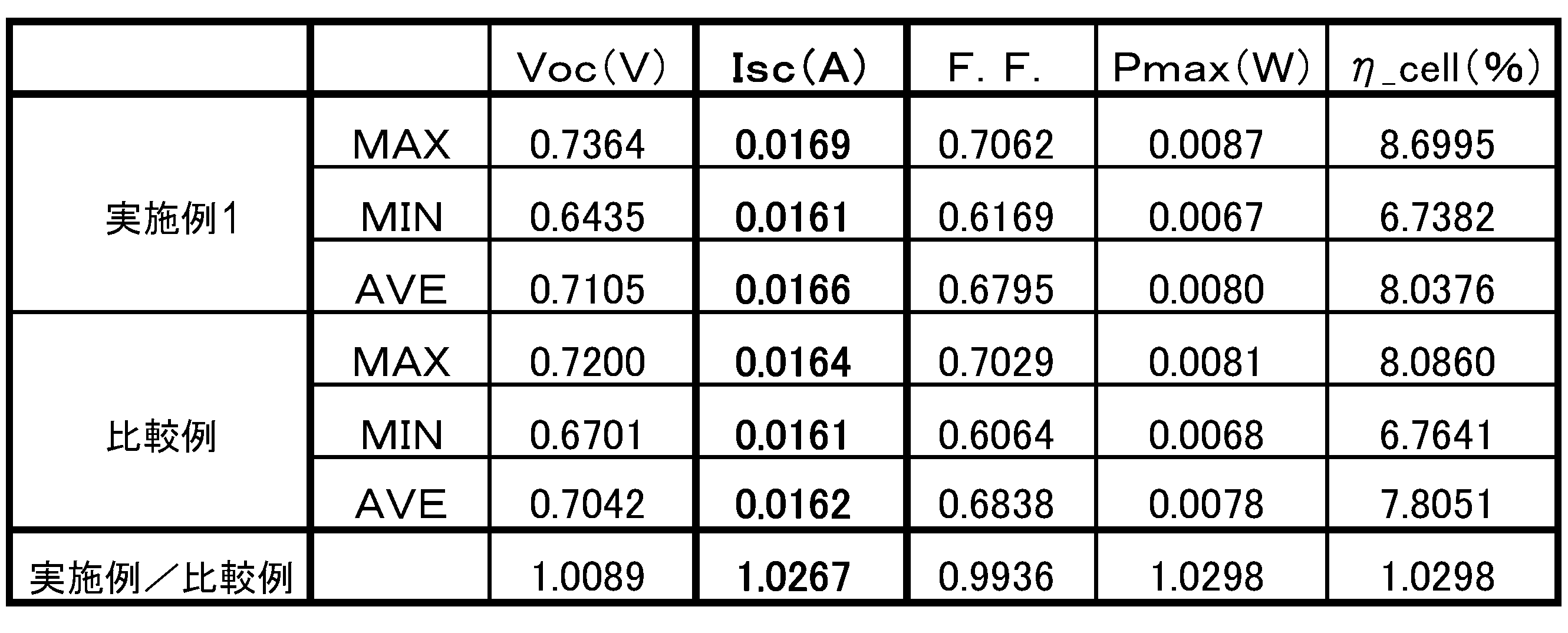
表1に示す測定値、計算値の項目は、Voc(V):開放電圧、Isc(A):短絡電流、F.F.:曲線因子、Pmax:最大電力、η_cell(%):変換効率である。実施例1に係る光起電力装置は、比較例に係る光起電力装置と比較して、短絡電流(Isc)に関し、2.67%の向上が確認できた。これは、大気、反射防止層、ガラス基板へと太陽光が進行する際に、反射防止層とガラス基板との界面での屈折率変化が、可視光に対して階段状に変化せず、微細な凹凸によって平均的屈折率が徐々に変化した結果、より大きな反射防止効果が得られたためと考えられる。
また、実施例1に係る光起電力装置は、プレッシャークッカー試験においても、時間の経過に伴う短絡電流(Isc)の低下は認められず、高い信頼性を有していることが確認できた。
本実施の形態に係る反射防止層14は、前述のように、空孔14aが形成されている多孔質層である。これにより、反射防止層14の屈折率を材質を変えずに適宜小さくできる。
図4は、反射防止層の一例の断面TEM写真を示す図である。図4に示す反射防止層は、空孔のサイズが約100nm×10nm程度であり、空孔率が10%程度と見積もられる。この場合、空孔の平均径は、測定箇所によって変化するが、10~100nmの範囲と捉えることができる。
空孔は、その平均径が、ガラス基板の凹凸の二乗平均平方根粗さRMSよりも小さくなるように形成されていてもよい。これにより、反射防止層の屈折率を小さくできるとともに、反射防止層自体の強度の低下を抑制できる。
なお、反射防止層14が多孔質層の場合、受光側からガラス基板側へ向かって、空孔14aの占める割合が段階的にまたは連続的に小さくなるように構成されていてもよい。これにより、反射防止層14における反射率を更に下げることができる。
反射防止層14は、受光側からガラス基板側へ向かって、屈折率が段階的にまたは連続的に大きくなるように構成されていてもよい。これにより、反射防止層14における反射率を更に下げることができる。
反射防止層14は、密度が2.4g/cm3以下の二酸化ケイ素を主成分とする材料で構成されており、その厚みが60~200nmの範囲であってもよい。これにより、ガラス基板12と組成が似た材料で反射防止層14を構成するため、ガラス基板12と反射防止層14との密着性を向上できる。また、反射防止層14により、ガラス基板12にアルカリ金属が含まれている場合であっても、アルカリ金属の析出が抑制され、ガラス基板12の白濁を防止することができる。
(実施例2)
次に、実施例2に係る太陽電池モジュール100について説明する。以下では、前述の実施の形態や実施例1に係る光起電力装置10と同様の構成については説明を適宜省略する。
次に、実施例2に係る太陽電池モジュール100について説明する。以下では、前述の実施の形態や実施例1に係る光起電力装置10と同様の構成については説明を適宜省略する。
図5は、実施例2に係る太陽電池モジュールの上面図である。図6(a)は、実施例2に係る太陽電池モジュールの断面図、図6(b)は、図6(a)のA領域の拡大図である。なお、図5に示す太陽電池モジュールは、受光面と反対側の裏面側から見たものである。
実施例2に係る太陽電池モジュール100は、光起電力装置10、配線材30、充填材32、および保護材としての裏面部材34を備える。
光起電力装置10は、前述のように、ガラス基板12と、ガラス基板12の受光面12a側に形成されている反射防止層14と、ガラス基板12の受光面12aと反対側に設けられ、光を電気に変える光起電力素子16と、を備える。
本実施例では、支持部材としてのガラス基板12の一つの主面上に、光起電力素子16としての単結晶Si太陽電池セルがマトリックス状に複数配置され、これらのセルがガラス基板12と接合される。また、ガラス基板12の他方の主面(太陽光入射面)には凹凸が形成され、その凹凸面上に低屈折率の反射防止層(Anti-Reflective coat)14が形成されている。
また、光起電力装置10において、それぞれの太陽電池セルは、光入射側と反対の面のみに、配線材30としての櫛型の正負電極(Anode/Cathode)が設けられたIBC(Interdigitated Back Contact)構造を有している。各太陽電池セルは、導電部材(Conducting wire)36を介して、直列および並列に接続されている。
さらに各太陽電池セル間、および裏面部材34としてのカバーガラス(Cover glass)と太陽電池セルとの間には、充填材32としてのEVA(エチレン酢酸ビニル共重合体)が充填され、外部環境からの封止構造が形成されている。
ガラス基板12の太陽光入射側(受光面12a側)に設けられた凹凸の大きさは、二乗平均平方根粗さRMSが0.5μmであり、酸化アルミニウム粒子を用いたサンドブラストにより形成されている。また、この凹凸上の反射防止層14は、密度2.2g/cm3、膜厚180nmのSiO2を主成分とする層であり、単結晶Siセルにおける太陽光の透過損失が生じる長波長光(主に波長が800nm以上の光)の反射を抑制するに適した膜厚となっている。従来の単結晶Si太陽電池では、セルの厚さが200μm前後、あるいはそれ以上であり、これを薄くすると光閉じ込め効果が著しく低下していた。しかしながら、本実施例により、厚さ50μmの単結晶Siでも高い光閉じ込め効果が得られた。
単結晶Siセルは、略正方形の形状であり、光入射面にI(Intrinsic)タイプのアモルファスSi層と窒化Si層をパッシベーション膜として形成した後、陽極接合法を用いて、ガラス基板12と接合されている。単結晶Siセルとガラス基板12との接合には、フッ素系の樹脂を用いたり、ガラスフリットを用いたりすることも可能である。単結晶Siセルの裏面構造であるIBC構造は、フォトリソグラフィを用いて形成されている。そして、単結晶Siセルの両端のアノード電極30aおよびカソード電極30bを介して発電電流が取り出される。
(実施例3)
次に、実施例3に係る太陽電池モジュール200について説明する。以下では、前述の実施の形態や各実施例に係る構成と同様の構成については説明を適宜省略する。
次に、実施例3に係る太陽電池モジュール200について説明する。以下では、前述の実施の形態や各実施例に係る構成と同様の構成については説明を適宜省略する。
図7は、実施例3に係る太陽電池モジュールの上面図である。図8(a)は、実施例3に係る太陽電池モジュールの断面図、図8(b)は、図8(a)のB領域の拡大図である。なお、図7に示す太陽電池モジュールは、受光面と反対側の裏面側から見たものである。
実施例3に係る太陽電池モジュール200は、ボトムセルとして第1の光起電力素子16である単結晶Si太陽電池セルと、トップセルとして第2の光起電力素子17である集積型アモルファスSi太陽電池とを有する。単結晶Si太陽電池セルおよび集積型アモルファスSi太陽電池は、光入射面であるガラス基板12に対して平行に2段に配置されている。また、集積型アモルファスSi太陽電池は、単結晶Si太陽電池セルよりも光入射面側に配置されている。
集積型アモルファスSi太陽電池は、ガラス基板12上に、透光性導電酸化膜(TCO)、アモルファスSi、透光性導電酸化膜を順次形成する工程と、積層されたそれら各層(膜)にレーザパターニング法により集積構造を形成する工程と、を経て作成されている。本実施例では、ガラス基板12に設けられた凹凸の大きさは、実施例2と同じRMSが0.5μmであるが、反射防止層14は短波長光の反射防止も求められるため、90nmとしている。
また、単結晶Si太陽電池セルと集積型アモルファスSi太陽電池とは、電気的に完全に絶縁され、発電電力はそれぞれ別個に取り出されている。具体的には、単結晶Si太陽電池セルにおいては、両端のアノード電極30aおよびカソード電極30bを介して発電電流が取り出される。一方、集積型アモルファスSi太陽電池においては、両端のアノード電極31aおよびカソード電極31bを介して発電電流が取り出される。
通常のタンデム構造型太陽電池では、発電電流を一致させる必要があるが、本実施例に係る太陽電池モジュール200のような構造を用いることにより、通常のタンデム構造型太陽電池に比べ、トップセル/ボトムセルの電流設計の自由度が高くなり、各セルの発電能力を最大に発揮することができる。
以上、本発明を上述の実施の形態を参照して説明したが、本発明は上述の実施の形態に限定されるものではなく、実施の形態の構成を適宜組み合わせたものや置換したものについても本発明に含まれるものである。また、当業者の知識に基づいて実施の形態における組合せや処理の順番を適宜組み替えることや各種の設計変更等の変形を実施の形態に対して加えることも可能であり、そのような変形が加えられた実施の形態も本発明の範囲に含まれ得る。
上述の実施の形態に係る第1電極層18としては、酸化亜鉛(ZnO)の他、酸化スズ(SnO2)、酸化インジウム(In2O3)、酸化チタン(TiO2)、スズ酸亜鉛(Zn2SnO4)などの金属酸化物より選択された一種類あるいは複数種類の積層体により構成されていてもよい。なお、これらの金属酸化物には、フッ素(F)、スズ(Sn)、アルミニウム(Al)、ガリウム(Ga)、ニオブ(Nb)などがドープされていてもよい。
また、上述の実施の形態では、ガラス基板の受光面側に設けられた微細な凹凸は、サンドブラスト処理により形成されているが、フッ酸によるエッチングにより形成してもよい。
また、反射防止層は、所定の粒径(粒子サイズ)を有するシリコン粒子を主成分とする液状材料を、ガラス基板上に塗布し、焼成して形成してもよい。この場合には、隣接するシリコン粒子間に生じる空隙が、反射防止層としての空隙に相当する。
なお、以下の組合せによる光起電力装置についても本発明の範囲に含まれうる。
(1)光起電力装置は、
ガラス基板と、
前記ガラス基板の受光面側に形成されている反射防止層と、
前記ガラス基板の受光面と反対側に設けられ、光を電気に変える光起電力素子と、を備え、
前記反射防止層は、前記ガラス基板よりも屈折率が小さくなるように構成されており、
前記ガラス基板は、受光面側に、二乗平均平方根粗さRMSが100~1100nmの範囲の凹凸を有する。
ガラス基板と、
前記ガラス基板の受光面側に形成されている反射防止層と、
前記ガラス基板の受光面と反対側に設けられ、光を電気に変える光起電力素子と、を備え、
前記反射防止層は、前記ガラス基板よりも屈折率が小さくなるように構成されており、
前記ガラス基板は、受光面側に、二乗平均平方根粗さRMSが100~1100nmの範囲の凹凸を有する。
二乗平均平方根粗さRMSが100nm未満であると、反射防止層14との密着性の改善の効果が小さい。一方、二乗平均平方根粗さRMSが1100nmより大きいと、凹凸の大きさが可視光の波長よりも大きくなってしまうため、太陽光中の可視光は、傾斜した凹凸面で幾何学反射し反射率が高まるため、透過光量が減少する。
(2)前記反射防止層は、空孔が形成されている多孔質層である(1)に記載の光起電力装置であってもよい。これにより、反射防止層の屈折率を材質を変えずに適宜小さくできる。
(3)前記空孔は、その平均径が、前記ガラス基板の凹凸の二乗平均平方根粗さRMSよりも小さくなるように形成されている(2)に記載の光起電力装置であってもよい。これにより、反射防止層の屈折率を小さくできるとともに、反射防止層自体の強度の低下を抑制できる。
(4)前記多孔質層は、受光側からガラス基板側へ向かって、空孔の占める割合が段階的にまたは連続的に小さくなるように構成されている(2)または(3)に記載の光起電力装置であってもよい。これにより、反射防止層における反射率を更に下げることができる。
(5)前記反射防止層は、密度が2.4g/cm3以下の二酸化ケイ素を主成分とする材料で構成されており、その厚みが60~200nmの範囲である(1)乃至(4)のいずれか1項に記載の光起電力装置であってもよい。これにより、ガラス基板と組成が似た材料で反射防止層を構成するため、ガラス基板と反射防止層との密着性を向上できる。また、反射防止層により、ガラス基板にアルカリ金属が含まれている場合であっても、アルカリ金属の析出が抑制され、ガラス基板の白濁を防止することができる。
10 光起電力装置、 12 ガラス基板、 12a 受光面、 14 反射防止層、 14a 空孔、 16 光起電力素子、 18 第1電極層、 20 半導体層、 22 第2電極層、 24 アモルファスシリコン半導体、 26 微結晶シリコン半導体。
本発明は、太陽電池に利用できる。
Claims (5)
- ガラス基板と、
前記ガラス基板の受光面側に形成されている反射防止層と、
前記ガラス基板の受光面と反対側に設けられ、光を電気に変える光起電力素子と、を備え、
前記反射防止層は、前記ガラス基板よりも屈折率が小さくなるように構成されており、
前記ガラス基板は、受光面側に、二乗平均平方根粗さRMSが100~1100nmの範囲の凹凸を有することを特徴とする光起電力装置。 - 前記反射防止層は、空孔が形成されている多孔質層であることを特徴とする請求項1に記載の光起電力装置。
- 前記空孔は、その平均径が、前記ガラス基板の凹凸の二乗平均平方根粗さRMSよりも小さくなるように形成されていることを特徴とする請求項2に記載の光起電力装置。
- 前記多孔質層は、受光側からガラス基板側へ向かって、空孔の占める割合が段階的にまたは連続的に小さくなるように構成されていることを特徴とする請求項2または3に記載の光起電力装置。
- 前記反射防止層は、密度が2.4g/cm3以下の二酸化ケイ素を主成分とする材料で構成されており、その厚みが60~200nmの範囲であることを特徴とする請求項1乃至4のいずれか1項に記載の光起電力装置。
Applications Claiming Priority (2)
| Application Number | Priority Date | Filing Date | Title |
|---|---|---|---|
| JP2011166982A JP2014199828A (ja) | 2011-07-29 | 2011-07-29 | 光起電力装置 |
| JP2011-166982 | 2011-07-29 |
Publications (1)
| Publication Number | Publication Date |
|---|---|
| WO2013018287A1 true WO2013018287A1 (ja) | 2013-02-07 |
Family
ID=47628839
Family Applications (1)
| Application Number | Title | Priority Date | Filing Date |
|---|---|---|---|
| PCT/JP2012/004485 Ceased WO2013018287A1 (ja) | 2011-07-29 | 2012-07-11 | 光起電力装置 |
Country Status (2)
| Country | Link |
|---|---|
| JP (1) | JP2014199828A (ja) |
| WO (1) | WO2013018287A1 (ja) |
Cited By (2)
| Publication number | Priority date | Publication date | Assignee | Title |
|---|---|---|---|---|
| CN105393367A (zh) * | 2013-06-17 | 2016-03-09 | 株式会社钟化 | 太阳能电池组件及太阳能电池组件的制造方法 |
| CN121398148A (zh) * | 2025-12-22 | 2026-01-23 | 晶科能源(海宁)有限公司 | 光伏组件 |
Citations (4)
| Publication number | Priority date | Publication date | Assignee | Title |
|---|---|---|---|---|
| JP2005099693A (ja) * | 2003-09-05 | 2005-04-14 | Hitachi Chem Co Ltd | 反射防止膜形成用組成物及びそれを用いた反射防止膜の製造方法、光学部品、太陽電池ユニット |
| JP2009088503A (ja) * | 2007-09-14 | 2009-04-23 | Mitsubishi Chemicals Corp | 太陽電池用積層カバー基板、太陽電池、並びに、太陽電池用積層カバー基板の製造方法 |
| JP2011049460A (ja) * | 2009-08-28 | 2011-03-10 | Mitsubishi Heavy Ind Ltd | 光電変換装置及び透明電極層付き基板 |
| JP2011111533A (ja) * | 2009-11-26 | 2011-06-09 | Asahi Kasei E-Materials Corp | 機能性塗膜 |
-
2011
- 2011-07-29 JP JP2011166982A patent/JP2014199828A/ja not_active Withdrawn
-
2012
- 2012-07-11 WO PCT/JP2012/004485 patent/WO2013018287A1/ja not_active Ceased
Patent Citations (4)
| Publication number | Priority date | Publication date | Assignee | Title |
|---|---|---|---|---|
| JP2005099693A (ja) * | 2003-09-05 | 2005-04-14 | Hitachi Chem Co Ltd | 反射防止膜形成用組成物及びそれを用いた反射防止膜の製造方法、光学部品、太陽電池ユニット |
| JP2009088503A (ja) * | 2007-09-14 | 2009-04-23 | Mitsubishi Chemicals Corp | 太陽電池用積層カバー基板、太陽電池、並びに、太陽電池用積層カバー基板の製造方法 |
| JP2011049460A (ja) * | 2009-08-28 | 2011-03-10 | Mitsubishi Heavy Ind Ltd | 光電変換装置及び透明電極層付き基板 |
| JP2011111533A (ja) * | 2009-11-26 | 2011-06-09 | Asahi Kasei E-Materials Corp | 機能性塗膜 |
Cited By (4)
| Publication number | Priority date | Publication date | Assignee | Title |
|---|---|---|---|---|
| CN105393367A (zh) * | 2013-06-17 | 2016-03-09 | 株式会社钟化 | 太阳能电池组件及太阳能电池组件的制造方法 |
| CN105393367B (zh) * | 2013-06-17 | 2017-06-09 | 株式会社钟化 | 太阳能电池组件及太阳能电池组件的制造方法 |
| TWI609498B (zh) * | 2013-06-17 | 2017-12-21 | 鐘化股份有限公司 | Solar cell module and solar cell module manufacturing method |
| CN121398148A (zh) * | 2025-12-22 | 2026-01-23 | 晶科能源(海宁)有限公司 | 光伏组件 |
Also Published As
| Publication number | Publication date |
|---|---|
| JP2014199828A (ja) | 2014-10-23 |
Similar Documents
| Publication | Publication Date | Title |
|---|---|---|
| JP5150473B2 (ja) | 積層型光電変換装置 | |
| CN100435357C (zh) | 串联薄膜太阳能电池 | |
| CN102934234B (zh) | 使用增强的光捕获方案的薄膜光伏器件 | |
| JP4940309B2 (ja) | 太陽電池 | |
| JPWO2007040065A1 (ja) | 太陽電池及び太陽電池モジュール | |
| WO2009116578A1 (ja) | 太陽電池 | |
| CN101246928A (zh) | 薄膜硅太阳能电池的背接触层 | |
| CN101246914A (zh) | 薄膜太阳能电池的背反射层 | |
| CN104321882A (zh) | 用于光伏器件的混合型接触件和光伏器件的形成方法 | |
| Oyama et al. | Requirements for TCO substrate in Si-based thin film solar cells-toward tandem | |
| JP2014199828A (ja) | 光起電力装置 | |
| JP2011187495A (ja) | 太陽電池モジュール | |
| JP5490031B2 (ja) | 光起電力装置および光起電力モジュール | |
| JP5542025B2 (ja) | 光電変換装置 | |
| JP2011054971A (ja) | 太陽電池 | |
| JP2012019128A (ja) | 薄膜光電変換装置 | |
| CN101777588A (zh) | 光散射多层结构及其制造方法 | |
| JP2012089712A (ja) | 薄膜太陽電池およびその製造方法 | |
| JP2014011307A (ja) | 薄膜太陽電池およびその製造方法、薄膜太陽電池モジュール | |
| JP5542038B2 (ja) | 薄膜太陽電池およびその製造方法、薄膜太陽電池モジュール | |
| TWI470814B (zh) | 太陽能電池 | |
| KR20130064658A (ko) | 태양전지 모듈 | |
| JP2011222589A (ja) | 光起電力装置およびその製造方法 | |
| CN208111457U (zh) | 一种带陷光结构的光伏组件 | |
| JP5563850B2 (ja) | 光電変換装置およびその製造方法 |
Legal Events
| Date | Code | Title | Description |
|---|---|---|---|
| 121 | Ep: the epo has been informed by wipo that ep was designated in this application |
Ref document number: 12820695 Country of ref document: EP Kind code of ref document: A1 |
|
| NENP | Non-entry into the national phase |
Ref country code: DE |
|
| 122 | Ep: pct application non-entry in european phase |
Ref document number: 12820695 Country of ref document: EP Kind code of ref document: A1 |
|
| NENP | Non-entry into the national phase |
Ref country code: JP |