WO2013015209A1 - 液晶表示装置 - Google Patents
液晶表示装置 Download PDFInfo
- Publication number
- WO2013015209A1 WO2013015209A1 PCT/JP2012/068423 JP2012068423W WO2013015209A1 WO 2013015209 A1 WO2013015209 A1 WO 2013015209A1 JP 2012068423 W JP2012068423 W JP 2012068423W WO 2013015209 A1 WO2013015209 A1 WO 2013015209A1
- Authority
- WO
- WIPO (PCT)
- Prior art keywords
- output gradation
- gradation
- value
- voltage
- output
- Prior art date
- Legal status (The legal status is an assumption and is not a legal conclusion. Google has not performed a legal analysis and makes no representation as to the accuracy of the status listed.)
- Ceased
Links
Images









Classifications
-
- G—PHYSICS
- G09—EDUCATION; CRYPTOGRAPHY; DISPLAY; ADVERTISING; SEALS
- G09G—ARRANGEMENTS OR CIRCUITS FOR CONTROL OF INDICATING DEVICES USING STATIC MEANS TO PRESENT VARIABLE INFORMATION
- G09G3/00—Control arrangements or circuits, of interest only in connection with visual indicators other than cathode-ray tubes
- G09G3/20—Control arrangements or circuits, of interest only in connection with visual indicators other than cathode-ray tubes for presentation of an assembly of a number of characters, e.g. a page, by composing the assembly by combination of individual elements arranged in a matrix no fixed position being assigned to or needed to be assigned to the individual characters or partial characters
- G09G3/34—Control arrangements or circuits, of interest only in connection with visual indicators other than cathode-ray tubes for presentation of an assembly of a number of characters, e.g. a page, by composing the assembly by combination of individual elements arranged in a matrix no fixed position being assigned to or needed to be assigned to the individual characters or partial characters by control of light from an independent source
- G09G3/36—Control arrangements or circuits, of interest only in connection with visual indicators other than cathode-ray tubes for presentation of an assembly of a number of characters, e.g. a page, by composing the assembly by combination of individual elements arranged in a matrix no fixed position being assigned to or needed to be assigned to the individual characters or partial characters by control of light from an independent source using liquid crystals
- G09G3/3611—Control of matrices with row and column drivers
- G09G3/3614—Control of polarity reversal in general
-
- G—PHYSICS
- G09—EDUCATION; CRYPTOGRAPHY; DISPLAY; ADVERTISING; SEALS
- G09G—ARRANGEMENTS OR CIRCUITS FOR CONTROL OF INDICATING DEVICES USING STATIC MEANS TO PRESENT VARIABLE INFORMATION
- G09G3/00—Control arrangements or circuits, of interest only in connection with visual indicators other than cathode-ray tubes
- G09G3/20—Control arrangements or circuits, of interest only in connection with visual indicators other than cathode-ray tubes for presentation of an assembly of a number of characters, e.g. a page, by composing the assembly by combination of individual elements arranged in a matrix no fixed position being assigned to or needed to be assigned to the individual characters or partial characters
- G09G3/2003—Display of colours
-
- G—PHYSICS
- G09—EDUCATION; CRYPTOGRAPHY; DISPLAY; ADVERTISING; SEALS
- G09G—ARRANGEMENTS OR CIRCUITS FOR CONTROL OF INDICATING DEVICES USING STATIC MEANS TO PRESENT VARIABLE INFORMATION
- G09G3/00—Control arrangements or circuits, of interest only in connection with visual indicators other than cathode-ray tubes
- G09G3/20—Control arrangements or circuits, of interest only in connection with visual indicators other than cathode-ray tubes for presentation of an assembly of a number of characters, e.g. a page, by composing the assembly by combination of individual elements arranged in a matrix no fixed position being assigned to or needed to be assigned to the individual characters or partial characters
- G09G3/34—Control arrangements or circuits, of interest only in connection with visual indicators other than cathode-ray tubes for presentation of an assembly of a number of characters, e.g. a page, by composing the assembly by combination of individual elements arranged in a matrix no fixed position being assigned to or needed to be assigned to the individual characters or partial characters by control of light from an independent source
- G09G3/36—Control arrangements or circuits, of interest only in connection with visual indicators other than cathode-ray tubes for presentation of an assembly of a number of characters, e.g. a page, by composing the assembly by combination of individual elements arranged in a matrix no fixed position being assigned to or needed to be assigned to the individual characters or partial characters by control of light from an independent source using liquid crystals
- G09G3/3611—Control of matrices with row and column drivers
- G09G3/3648—Control of matrices with row and column drivers using an active matrix
-
- G—PHYSICS
- G09—EDUCATION; CRYPTOGRAPHY; DISPLAY; ADVERTISING; SEALS
- G09G—ARRANGEMENTS OR CIRCUITS FOR CONTROL OF INDICATING DEVICES USING STATIC MEANS TO PRESENT VARIABLE INFORMATION
- G09G2320/00—Control of display operating conditions
- G09G2320/02—Improving the quality of display appearance
- G09G2320/028—Improving the quality of display appearance by changing the viewing angle properties, e.g. widening the viewing angle, adapting the viewing angle to the view direction
Definitions
- the present invention relates to a liquid crystal display device, and more particularly to a liquid crystal display device that performs display of a target luminance by dividing it into a relatively bright luminance display and a relatively dark luminance display in order to improve viewing angle characteristics. .
- a method of “one pixel is composed of a plurality of (typically two) sub-picture elements and the liquid crystal is driven so that the brightness of the plurality of sub-picture elements is different from each other” hereinafter referred to as “the picture element”.
- “Space division method”) and “with respect to display in each picture element, a unit period (a period during which an image for one screen is displayed) is displayed with relatively bright luminance hereinafter referred to as“ bright display ”).
- a method in which display of desired luminance is performed by dividing into a period for performing display and a period for performing display of relatively dark luminance (hereinafter referred to as “dark display”). It is known as a technique for improving viewing angle characteristics.
- FIG. 13 is a circuit diagram showing a configuration of a part for forming one picture element (hereinafter referred to as “picture element part”) in the liquid crystal display device adopting the space division method.
- the picture element unit 80 includes two sub picture element parts (a first sub picture element part PIX81 and a second sub picture element part PIX82). Both sub picture element portions (PIX81, PIX82) are thin film transistors (T81, PIX81) having a gate electrode connected to a gate bus line (scanning signal line) GL and a source electrode connected to a source bus line (video signal line) SL.
- T81, PIX81 thin film transistors having a gate electrode connected to a gate bus line (scanning signal line) GL and a source electrode connected to a source bus line (video signal line) SL.
- pixel electrodes E81, E82
- pixel electrodes E81, E82
- liquid crystal capacitors Clc81, Clc82
- auxiliary capacitors Ccs81, Ccs82
- pixel electrodes E81, E82
- CS bus lines auxiliary capacitor lines
- a pixel capacitor is formed by the liquid crystal capacitor and the auxiliary capacitor, and a constant voltage VCOM is applied to the common electrode EC. In such a configuration, when the gate bus line GL is selected, the thin film transistors T81 and T82 are turned on.
- the first sub picture element portion PIX81 and the source electrode of the thin film transistor T82 in the second sub picture element portion PIX82 are connected to the same source bus line SL, the first sub picture element portion PIX81.
- the voltage of the pixel electrode E81 is equal to the voltage of the pixel electrode E82 in the second sub picture element unit PIX82.
- the voltage of the pixel electrode E81 and the voltage of the pixel electrode E82 fluctuate in opposite directions. Accordingly, the pixel electrode E81 and the pixel electrode E82 have different voltages, and the first sub-picture element unit PIX81 and the second sub-picture element unit PIX82 have different luminance. As a result, viewing angle characteristics are improved.
- a unit period for displaying an image for one screen is composed of, for example, four frames.
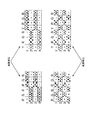
- the display state of each pixel changes as shown in FIG.
- FIG. 14 if there is a pixel whose display state changes such as “dark display, dark display, bright display, bright display”, it is displayed as “bright display, bright display, dark display, dark display”.
- Some pixels change state.
- the viewing angle characteristic is improved by displaying the target luminance using the bright display period and the dark display period. Note that the viewing angle characteristics are similarly improved when the display state changes in units of picture elements instead of in units of pixels.
- the voltage-transmittance characteristics are represented by two curves (two VT curves).
- two VT curves For example, when an input signal having a gradation value corresponding to the voltage indicated by reference numeral V1 in FIG. 15 is given, a VT curve indicated by reference numeral 83 indicates a pixel to be brightly displayed (hereinafter referred to as “bright pixel”).
- the source voltage is determined so that the transmittance indicated by reference numeral T1 can be obtained on the basis of the reference voltage, and the pixel to be darkly displayed (hereinafter referred to as “dark pixel”) is indicated by reference numeral T2 based on the VT curve indicated by reference numeral 84
- the source voltage is determined so that the transmittance is obtained.
- the correspondence between the input gradation (the gradation value indicated by the input signal) and the output gradation (the gradation value directly used for determining the source voltage) is indicated by reference numeral 85 in FIG.
- a dark pixel is represented by a curve as indicated by reference numeral 86 in FIG.
- gradation value conversion lookup table in which input gradations are associated with output gradations of bright pixels and dark pixels.
- FIG. 17 is a diagram schematically showing an example of a lookup table for gradation value conversion.
- a line denoted by reference numeral 87 means that “if the input gradation is 192, the output gradation is set to 240 for the bright pixel and the output gradation is set to 32 for the dark pixel”. ing. Therefore, in the case where the grayscale value conversion look-up table shown in FIG. 17 is used in the liquid crystal display device that employs the time division method, if data having an input grayscale of 192 is included, the data corresponds to the data.
- the change in the output gradation at the pixel is, for example, as shown in FIG.
- An invention of a liquid crystal display device that employs the time division method as described above in order to improve viewing angle characteristics is disclosed in, for example, Japanese Patent Application Laid-Open No. 7-121144.
- image display may be performed using a part of the display unit (typically, the central part) instead of performing image display using the entire display unit.
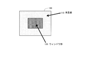
- a window unit 120 for displaying an image is provided at the center of the display unit 100, and a background color is displayed around the window unit 120.
- the background portion 110 is provided.
- the background portion 110 displays a predetermined color such as gray or black
- the window portion 120 displays a still image / moving image according to a user's request.
- attention is paid to eight pixels (2 columns ⁇ 4 rows of pixels) existing in the region denoted by reference numeral 88 in FIG. As for these eight pixels, as shown in FIG.
- one pixel includes a plurality of picture elements.
- FIG. 22 shows an example composed of four picture elements of blue and blue (B).
- one pixel is composed of three picture elements of red (R), green (G), and blue (B).
- the output gradation is 96 and the polarity is positive.
- column G1 the column of green picture elements in the first column in FIG. 21.
- FIG. 24 shows changes in the voltage (source voltage) of the source bus line SL and the voltage of the CS bus line CSL provided corresponding to the columns R1, G1, B1, R2, G2, and B2, respectively. Is shown.
- the time point at which writing to the (N + 2) th line is started is indicated by reference sign t0.
- the column R1 changes from a positive polarity voltage corresponding to the gradation value 96 to a positive polarity voltage corresponding to the gradation value 0.
- the voltage for negative polarity corresponding to the gradation value 96 changes to the voltage for negative polarity corresponding to the gradation value 240.
- the column B1 is the same as the column R1.
- the voltage for negative polarity corresponding to the gradation value 8 changes to the voltage for negative polarity corresponding to the gradation value 0.
- the column G2 changes from a positive polarity voltage corresponding to the gradation value 8 to a positive polarity voltage corresponding to the gradation value 32.
- the column B2 is the same as the column R2.
- the source voltage generally changes in the negative direction when shifting from the writing period to the background portion 110 to the writing period to the window portion 120.
- the picture element portion that forms one picture element is gated to the gate bus line GL, the source bus line SL, the common electrode EC, the CS bus line CSL, and the gate bus line GL.
- a thin film transistor (TFT) 101 having an electrode connected thereto and a source electrode connected to the source bus line SL, a pixel electrode 102 connected to the drain electrode of the thin film transistor 101, a pixel electrode 102 and a common electrode EC is formed.
- a parasitic capacitance is formed between the source bus line SL and the CS bus line CSL as indicated by reference numeral C9 in FIG.
- the source voltage generally changes in the negative direction. From the above, at the time point t0, due to the presence of the parasitic capacitance C9 between the source bus line SL and the CS bus line CSL, as indicated by reference numeral 90 in FIG. (Hereinafter referred to as “CS ripple”).
- the CS ripple is attenuated, that is, the magnitude of the CS ripple is gradually reduced.
- the gate bus line GL is in a non-selected state at the time point t1. Accordingly, since the thin film transistor 101 (see FIG. 25) is turned off, the pixel electrode voltages (VD (+) and VD ( ⁇ ) in FIG. 26) also change with the change in the voltage of the CS bus line CSL after time t1. Change. In the example shown in FIG.
- a voltage having a magnitude indicated by reference numeral 92 is originally applied although a voltage having a magnitude indicated by reference numeral 91 should be applied to the liquid crystal layer. Is applied to the liquid crystal layer.
- a voltage having a magnitude indicated by reference numeral 94 is originally applied although a voltage having a magnitude indicated by reference numeral 93 should be applied to the liquid crystal layer. Applied to the liquid crystal layer.
- the source voltage when the writing period to the window part 120 is shifted to the writing period to the background part 110, the source voltage generally changes in the positive direction. For this reason, as shown in FIG. 27, a positive CS ripple occurs at time t10 when the writing period to the background portion 110 starts. Due to the CS ripple, in the picture element portion where the polarity is to be positive, a voltage of the magnitude indicated by the reference numeral 95 should be applied to the liquid crystal layer, although the reference numeral 96 is the original. A voltage having the magnitude shown is applied to the liquid crystal layer.
- a voltage having a magnitude indicated by reference numeral 98 is originally applied although a voltage having a magnitude indicated by reference numeral 97 should be applied to the liquid crystal layer. Applied to the liquid crystal layer.
- an object of the present invention is to suppress the occurrence of horizontal stripes on the screen in a liquid crystal display device adopting a time division method in order to improve viewing angle characteristics.
- a plurality of video signal lines for transmitting a video signal and a plurality of scanning signal lines which are arranged so as to intersect the plurality of video signal lines and are selected by one horizontal scanning period. And forming a storage capacitor between the plurality of pixel electrodes provided corresponding to the intersections of the plurality of video signal lines and the plurality of scanning signal lines, respectively, and the plurality of pixel electrodes.
- a display unit including a plurality of auxiliary capacitance lines arranged so as to intersect with the plurality of video signal lines, and a voltage determined based on an input signal indicating a gradation value is applied to the pixel electrode;
- a liquid crystal display device that displays an image based on the input signal on the display unit by applying the video signal to the plurality of video signal lines, A video to be applied to the plurality of video signal lines by correcting the first output gradation determined based on the line data for each line data which is data for one horizontal scanning period included in the input signal.
- An output gradation correction processing unit for obtaining a second output gradation corresponding to the signal voltage;
- a horizontal scanning period in which the video signal is to be applied to the plurality of video signal lines based on line data on which processing for obtaining the second output gradation is performed is defined as a processing target horizontal scanning period, and the processing target A second output gray level obtained based on line data for the preceding horizontal scanning period for the plurality of video signal lines, wherein a horizontal scanning period one horizontal scanning period before the horizontal scanning period is defined as a preceding horizontal scanning period.
- the output The gradation correction processing unit obtains the second output gradation by correcting the first output gradation based on the voltage difference sum.
- the output gradation correction processing unit For the data corresponding to the pixel electrode to which a positive voltage is to be applied during the horizontal scan period to be processed among the line data, if the sum of the voltage differences is a positive value, the second output gray level is If the value is equal to or higher than the first output gradation and the voltage difference sum is a negative value, the second output gradation is set to a value equal to or lower than the first output gradation.
- the second output gray level is The second output gradation is set to a value equal to or higher than the first output gradation if the value is equal to or lower than the first output gradation and the voltage difference sum is a negative value.
- the output gradation correction processing unit increases the first output gradation as the absolute value of the voltage difference sum is larger for the plurality of data. And the difference between the second output gradation and the second output gradation.
- a correction addition / subtraction which is a combination of a value corresponding to the sum of the voltage differences and the first output gradation and a value used for correcting the first output gradation
- An output tone correction look-up table for storing correspondences with values;
- the output gradation correction processing unit includes a correction addition / subtraction value acquired from the output gradation correction lookup table based on a combination of a value corresponding to the voltage difference sum and the first output gradation, and the first A value obtained by the addition / subtraction process with the output gradation is defined as the second output gradation.
- the output gradation correction processing unit calculates a predetermined magnification according to the position in the display unit before performing the addition / subtraction process between the correction addition / subtraction value and the first output gradation. It is characterized by multiplying.
- a sixth aspect of the present invention is the fifth aspect of the present invention, A magnification lookup table for storing a correspondence relationship between a position in the display unit and a magnification used for correcting the correction addition / subtraction value;
- the output gradation correction processing unit multiplies the correction addition / subtraction value by a magnification obtained from the magnification lookup table based on a position in the display unit for each data.
- the first output gradation for bright display and the relatively dark display for performing relatively bright display as the first output gradation.
- the video signal voltage corresponding to the output gradation is applied to the pixel electrode corresponding to each data, and the dark display first output gradation is corrected during the remaining half of the plurality of frame periods.
- the video signal voltage corresponding to the second output gradation obtained by applying is applied to the pixel electrode corresponding to the data.
- the display unit includes a first display unit that displays an image based on a constant gradation value, and a second display unit that is an area other than the first display unit and displays an image based on an arbitrary gradation. It is characterized by the following.
- a display unit including a plurality of auxiliary capacitance lines arranged so as to intersect with the plurality of video signal lines, and a voltage determined based on an input signal indicating a gradation value is applied to the pixel electrode;
- a liquid crystal display driving method for displaying an image based on the input signal on the display unit by applying the video signal to the plurality of video signal lines, A video to be applied to the plurality of video signal lines by correcting the first output gradation determined based on the line data for each line data which is data for one horizontal scanning period included in the input signal.
- An output gradation correction step for obtaining a second output gradation corresponding to the signal voltage;
- a horizontal scanning period in which the video signal is to be applied to the plurality of video signal lines based on line data on which processing for obtaining the second output gradation is performed is defined as a processing target horizontal scanning period, and the processing target
- the output gradation correction step includes: It is determined based on the video signal voltage corresponding to the second output gradation obtained based on the line data for the preceding horizontal scanning period for the plurality of video signal lines and the line data for the processing target horizontal scanning period.
- a voltage difference sum calculating step for obtaining a sum of differences from the video signal voltage corresponding to the first output gradation as a voltage difference sum;
- a second output gradation calculation step for obtaining the second output gradation based on the total voltage difference.
- the second output tone calculation step For the data corresponding to the pixel electrode to which a positive voltage is to be applied during the horizontal scan period to be processed among the line data, if the sum of the voltage differences is a positive value, the second output gradation is If the value is greater than or equal to the first output tone and the voltage difference sum is a negative value, the second output tone is less than or equal to the first output tone, For the data corresponding to the pixel electrode to which a negative voltage is to be applied during the horizontal scan period to be processed among the line data, if the sum of the voltage differences is a positive value, the second output gradation is The second output gradation is set to a value equal to or greater than the first output gradation if the value is equal to or less than the first output gradation and the voltage difference sum is a negative value.
- An eleventh aspect of the present invention is the ninth aspect of the present invention, Based on the gradation value indicated by each data included in the input signal, the first output gradation for bright display and the relatively dark display for performing relatively bright display as the first output gradation.
- a gradation value obtaining step for obtaining a first output gradation for dark display; An image for one screen is displayed over multiple frame periods, When attention is paid to each data included in the input signal, the second obtained by correcting the first output gradation for bright display during the half of the plurality of frame periods.
- the video signal voltage corresponding to the output gradation is applied to the pixel electrode corresponding to each data, and the dark display first output gradation is corrected during the remaining half of the plurality of frame periods.
- the video signal voltage corresponding to the second output gradation obtained by applying is applied to the pixel electrode corresponding to the data.
- the gradation value for determining the video signal voltage by correcting the gradation value (first output gradation) obtained based on the input signal. (Second output gradation) is obtained. More specifically, the first output gradation is calculated based on the sum of changes (voltage difference sum) of video signal voltages for all video signal lines during two consecutive horizontal scanning periods when it is assumed that no correction is made. Correction is performed to obtain the second output gradation.
- the total sum of changes in the video signal voltage for all video signal lines during two consecutive horizontal scanning periods is proportional to the magnitude of ripple (CS ripple) generated in the auxiliary capacitance wiring.
- the correction is performed in consideration of the total voltage difference as described above, so that even if a change occurs in the pixel electrode voltage after the end of the writing period to each line due to the CS ripple, the changed pixel electrode It is possible to make the voltage close to the voltage that should be originally applied to the pixel electrode. For this reason, by suitably correcting the gradation value, the occurrence of horizontal stripes on the screen, which has conventionally occurred when the change in the video signal voltage is biased, is suppressed.
- the first output gradation is corrected in consideration of the change direction of the pixel electrode voltage caused by the CS ripple in advance, and the second output gradation is obtained. For this reason, generation
- the larger the magnitude of CS ripple that is expected to occur when correction is not performed the larger the first output gradation is corrected, and the second output gradation is obtained. It is done. For this reason, generation
- the magnification determined according to the position in the display unit is multiplied by the correction addition / subtraction value for obtaining the second output gradation.
- the second output gradation is obtained in consideration of the difference in the CS ripple attenuation speed depending on the position in the display unit.
- the correspondence between the position in the display unit and the magnification is stored in the lookup table, thereby preventing the circuit from being complicated.
- a change in the video signal voltage between two consecutive horizontal scanning periods tends to be biased, so that horizontal stripes on the screen due to CS ripple are likely to occur.
- the occurrence of horizontal stripes on the screen is effectively suppressed.
- the same effect as that of the first aspect of the present invention can be achieved in the driving method of the liquid crystal display device.
- the same effect as in the second aspect of the present invention can be achieved in the method for driving the liquid crystal display device.
- the same effect as in the seventh aspect of the present invention can be achieved in the method for driving the liquid crystal display device.
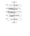
- FIG. 5 is a flowchart showing a procedure of a horizontal stripe correction process in an active matrix liquid crystal display device according to an embodiment of the present invention.
- it is a block diagram which shows the whole structure of a liquid crystal display device.
- it is a figure for demonstrating a CS bus line and CS trunk line.
- it is a block diagram which shows the structure of a display control circuit.
- FIG. 5 is a diagram illustrating a configuration example of a gradation value-voltage conversion lookup table in the embodiment.
- it is a figure which shows one structural example of the lookup table for positive polarity backgrounds.
- it is a figure which shows one structural example of the lookup table for negative polarity backgrounds.
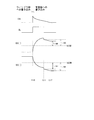
- the said embodiment it is a graph which shows the relationship between CS ripple amount and the source voltage change amount for 1 line. It is a signal waveform diagram for demonstrating the effect in the said embodiment.
- the 1st modification of the said embodiment it is a figure which shows one structural example of the look-up table for in-plane distribution correction
- FIG. 6 is a graph for explaining voltage-transmittance characteristics in a liquid crystal display device adopting a space division method or a time division method. It is a graph for demonstrating the relationship between the input gradation and the output gradation in the liquid crystal display device which employ
- FIG. 2 is a block diagram showing the overall configuration of an active matrix liquid crystal display device according to an embodiment of the present invention.
- the liquid crystal display device includes a display unit 100, a gate driver (scanning signal line driving circuit) 200, a source driver (video signal line driving circuit) 300, an auxiliary capacitance wiring driver 400, and a display control circuit 500. It has.
- the display unit 100 includes a plurality (i) of gate bus lines (scanning signal lines) GL1 to GLi, a plurality (j) of source bus lines (video signal lines) SL1 to SLj, and a gate bus line GL1.
- a plurality of (i ⁇ j) picture element portions provided corresponding to the intersections of .about.GLi and source bus lines SL1 to SLj are formed.
- the plurality of picture element portions are arranged in a matrix to form a pixel array.
- CS bus lines auxiliary capacitance lines
- Each CS bus line is arranged to extend in parallel with the gate bus line.
- a CS trunk line 11 is disposed in a region outside the display unit 100 on the panel substrate 10 as a component for applying a desired voltage to the CS bus lines CSL1 to CSLi.
- Each CS bus line is connected to the CS trunk line 11 in the vicinity of both ends of the display unit 100.
- the CS trunk line 11 is connected to the auxiliary capacitance wiring driver 400. As described above, the CS bus lines CSL1 to CSLi and the auxiliary capacitance wiring driver 400 are connected via the CS trunk line 11.
- FIG. 25 is a circuit diagram showing the configuration of the picture element portion.
- each pixel unit includes a gate bus line GL, a source bus line SL, a common electrode EC, a CS bus line CSL, a gate bus connected to the gate bus line GL and a source bus.
- a thin film transistor (TFT) 101 having a source electrode connected to the line SL, a pixel electrode 102 connected to the drain electrode of the thin film transistor 101, a liquid crystal capacitor 103 formed by the pixel electrode 102 and the common electrode EC, and a pixel electrode 102 and an auxiliary capacitor 104 formed by the CS bus line CSL.
- TFT thin film transistor
- a pixel capacitor is formed by the liquid crystal capacitor 103 and the auxiliary capacitor 104.
- the pixel value is set to the pixel capacitance based on the video signal that the source electrode of the thin film transistor 101 receives from the source bus line SL. Is held.
- a time division method is adopted as a technique for improving the viewing angle characteristics.
- a unit period for displaying an image for one screen is composed of four frames (see FIGS. 14 and 18).
- a window portion 120 for displaying an image is provided at the center portion of the display portion 100, and a background color is displayed around the window portion 120.
- a background part 110 is provided.
- one pixel is composed of three picture elements of red (R), green (G), and blue (B).
- the first display unit is realized by the background unit 110
- the second display unit is realized by the window unit 120.
- the display control circuit 500 receives an image signal DAT and a timing signal group TG such as a horizontal synchronization signal and a vertical synchronization signal sent from the outside, and receives a digital video signal DV and a gate start pulse signal for controlling the operation of the gate driver 200.
- a line control signal SCS is output.
- the gate driver 200 receives the gate start pulse signal GSP and the gate clock signal GCK output from the display control circuit 500, and applies a scanning signal to each gate bus line.
- the gate driver 200 selects the gate bus line every other row. That is, “the first line, the third line,..., The i-3 line, the i-1 line, the second line, the fourth line,..., The i-2 line, the i line”. Each gate bus line is selected in order.
- the source driver 300 receives the digital video signal DV, the source start pulse signal SSP, the source clock signal SCK, and the latch strobe signal LS output from the display control circuit 500, and applies a driving video signal to each source bus line.
- the auxiliary capacitance line driver 400 controls the voltage applied to the CS bus line CSL based on the CS bus line control signal SCS output from the display control circuit 500.
- the voltage applied to the CS bus line CSL is controlled, the scanning signal is applied to each gate bus line GL, and the drive video signal is applied to each source bus line SL.
- An image based on the image signal DAT sent from the outside is displayed on the display unit 100.
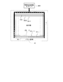
- FIG. 4 is a block diagram showing a configuration of the display control circuit 500 in the present embodiment.
- the display control circuit 500 includes an interface unit 51, a gradation value acquisition unit 52, a horizontal stripe correction processing unit 53, and a timing generator 54.
- the gradation value acquisition unit 52 includes a gradation value conversion lookup table 521.
- the horizontal stripe correction processing unit 53 includes a CS ripple estimation unit 531, a gradation value-voltage conversion lookup table 532, a gradation value correction unit 533, a positive polarity background lookup table 534, and a negative polarity background lookup table 535. It is included.
- the interface unit 51 receives the image signal DAT and the timing signal group TG from the outside, and supplies them to the gradation value acquisition unit 52 and the timing generator 54 as appropriate.
- the gradation value acquisition unit 52 refers to the lookup table 521 for gradation value conversion, and based on the input gradation that is the gradation indicated by the image signal DAT, the output gradation for the bright pixel (first for bright display). Output gradation) and output gradation for dark pixels (first output gradation for dark display) are acquired.
- the gradation value conversion lookup table 521 stores data in which the input gradation is associated with the output gradation of the bright pixel and the dark pixel (see FIG. 17).
- the horizontal stripe correction processing unit 53 suppresses the occurrence of horizontal stripes on the screen due to the CS ripple, so that the gradation value acquired by the gradation value acquisition unit 52 (that is, the gradation value conversion lookup table 521). (Corrected output gradation) is corrected, and the corrected gradation value is output as a digital video signal DV.
- the gradation value acquired by the gradation value acquisition unit 52 is referred to as “first output gradation”
- the gradation value obtained by the correction processing by the horizontal line correction processing unit 53 is referred to as “second output level”. Key.
- the gradation value-voltage conversion lookup table 532 stores data in which gradation values and source voltages are associated with each other.
- the CS ripple estimation unit 531 estimates the magnitude of CS ripple generated in each CS bus line CSL while referring to the gradation value-voltage conversion lookup table 532.
- the numerical value of the CS ripple is referred to as “CS ripple amount”.
- the positive polarity background lookup table 534 and the negative polarity background lookup table 535 store data in which “combination of CS ripple amount and background gradation” and “correction addition / subtraction value” are associated with each other. .
- the correction addition / subtraction value is a value used in a calculation process for obtaining the second output gradation in a horizontal stripe correction process described later.
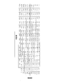
- FIG. 6 is a diagram illustrating a configuration example of the positive polarity background lookup table 534.
- FIG. 7 is a diagram illustrating a configuration example of the negative polarity background lookup table. For example, the data indicated by reference numeral 72 in FIG.
- the gradation value correction unit 533 obtains a correction addition / subtraction value by referring to the positive polarity background lookup table 534 and the negative polarity background lookup table 535 based on the CS ripple amount estimated by the CS ripple estimation unit 531. A second output gradation for each picture element is obtained using the correction addition / subtraction value. Details of processing performed by the CS ripple estimation unit 531 and the gradation value correction unit 533 will be described later.
- the positive polarity background lookup table 534 and the negative polarity background lookup table 535 are collectively referred to as a “polarity background lookup table”.
- the timing generator 54 generates the above-described source start pulse signal SSP, source clock signal SCK, latch strobe signal LS, gate start pulse signal GSP, gate clock signal GCK, and CS bus line control signal SCS, and outputs them. .
- an output tone correction processing unit is realized by the horizontal stripe correction processing unit 53, and an output tone correction lookup table is formed by the positive polarity background lookup table 534 and the negative polarity background lookup table 535. Is realized.
- FIG. 1 is a flowchart showing a procedure of lateral stripe correction processing in the present embodiment.
- the lateral stripe correction process is performed by the lateral stripe correction processing unit 53 described above.
- FIG. 1 shows a procedure for one line, and the processing from step S110 to step S130 is repeated during the operation of the liquid crystal display device.
- the line (processing) in which the first output gradation is acquired by the CS ripple estimation unit 531 The magnitude of CS ripple (CS ripple amount) generated in the CS bus line CSL provided corresponding to the target line) is estimated (step S110).
- the CS ripple estimation unit 531 first determines, for each source bus line SL, “source voltage one horizontal scanning period before the horizontal scanning period in which the processing target line is in the selected state” and “tone value acquisition unit 52. A difference from the “source voltage obtained on the basis of the acquired first output gradation” (hereinafter referred to as “source voltage change amount”) is obtained.
- the CS ripple estimation unit 531 converts the first output gradation acquired by the gradation value acquisition unit 52 into a source voltage, and the gradation value-voltage conversion lookup table as shown in FIG. 532 is referred to. Then, the CS ripple estimation unit 531 obtains the sum of the source voltage change amounts for all the source bus lines SL.
- the total sum of the source voltage change amounts is referred to as “one line source voltage change amount”.
- the horizontal scanning period in which the processing target line is selected corresponds to the processing target horizontal scanning period, and the horizontal scanning period one horizontal scanning period before the processing target horizontal scanning period corresponds to the preceding horizontal scanning period. Further, the amount of change in the source voltage for one line corresponds to the total voltage difference.
- the source voltage change amount for one line is obtained as follows.
- one pixel is composed of three picture elements, and the gate bus lines GL are selected every other row. Therefore, the “to the (M-2) th line” for 5760 source bus lines SL.
- the gradation value-voltage conversion lookup table 532 is referred to based on the “source voltage in the horizontal scanning period in which writing is performed” and “the first output gradation acquired by the gradation value acquisition unit 52 for the Mth line”. The total sum of the differences from the “source voltage obtained by this” is obtained as the source voltage change amount for one line.
- the “source voltage in the horizontal scanning period” is a voltage based on the second gradation. If the amount of change in the source voltage for one line is a positive value, writing to the processing target line causes a CS ripple so that the voltage of the CS bus line CSL increases. On the other hand, if the amount of change in the source voltage for one line is a negative value, writing to the processing target line causes a CS ripple so that the voltage of the CS bus line CSL decreases.
- the CS ripple estimation unit 531 estimates the CS ripple amount from the source voltage change amount for one line obtained as described above. As described above, in step S110, the CS ripple estimation unit 531 estimates the CS ripple amount.
- the gradation value correction unit 533 acquires correction addition / subtraction values from the polarity-specific background lookup table for each picture element included in the processing target line based on the CS ripple amount obtained in step S110. (Step S120).
- the positive polarity background look-up table 534 is referred to for a pixel whose polarity should be positive, and the negative polarity background look is referred to for a pixel whose polarity should be negative.
- the up table 535 is referred to.
- the gradation value correction unit 533 acquires the correction addition / subtraction value for each picture element.
- the second output gradation is calculated by the gradation value correcting unit 533 (step S130). Specifically, the tone value correcting unit 533 for each picture element included in the processing target line and the tone value (first output tone) acquired by the tone value acquiring unit 52 and the correction acquired in step S120.
- the second output gradation is calculated based on the addition / subtraction value. For example, if the gradation value acquired by the gradation value acquisition unit 52 is 15 and the correction addition / subtraction value acquired in step S120 is 3, the second output gradation is 18. For example, if the gradation value acquired by the gradation value acquisition unit 52 is 696 and the correction addition / subtraction value acquired in step S120 is ⁇ 55, the second output gradation is 641.
- step S130 the gradation value correction unit 533 calculates the second output gradation for each pixel. By calculating the second output gradation in this way, the horizontal stripe correction process is completed. As described above, the second output gradation obtained by the horizontal stripe correction process is output from the display control circuit 500 as the digital video signal DV.
- the horizontal axis is the CS ripple amount.
- the source voltage change amount may be set on the horizontal axis.
- the CS ripple amount is proportional to the source voltage change amount for one line
- the value corresponding to the source voltage change amount for one line can be used as the horizontal axis of the polarity-specific background lookup table. .
- gradation values for bright pixels and dark pixels (based on an input signal (image signal DAT)) ( After the first output gradation) is acquired, the gradation values for the bright pixel and the dark pixel are corrected as follows, so that the pixel elements included in the processing target line A gradation value (second output gradation) for determining the source voltage for writing is obtained.
- the magnitude of CS ripple (CS ripple amount) that is expected to occur in the CS bus line CSL when writing to the processing target line is estimated.
- the CS ripple amount is estimated based on “source voltage one horizontal scanning period before the horizontal scanning period in which writing to the processing target line is performed” and “source corresponding to the output gradation based on the input signal” for all source bus lines SL. This is done by adding all the differences from “voltage”. Then, in accordance with the magnitude of the CS ripple amount, the output gradation is corrected using the correction addition / subtraction value stored in the polarity-specific background lookup table.
- the data is stored in the polarity-specific background lookup table as follows. (1) The correction addition / subtraction value (absolute value) is increased as the CS ripple amount (absolute value) is increased.
- the sign of the correction addition / subtraction value is determined.
- (2-1) For picture elements whose polarity should be positive, if the CS ripple amount is a positive value, the correction addition / subtraction value is a positive value, and if the CS ripple amount is a negative value, the correction addition / subtraction is performed The value is negative.
- (2-2) For a pixel whose polarity should be negative, if the CS ripple amount is a positive value, the correction addition / subtraction value is a negative value, and if the CS ripple amount is a negative value, the correction addition / subtraction is performed The value is a positive value.
- the correction addition / subtraction value (absolute value) for the background gradation corresponding to the vicinity of the rise (inflection point) of the VT curve (see FIG. 15) is made relatively large.
- the change in the pixel electrode voltage caused by the CS ripple in each picture element portion is performed by correcting the output gradation in consideration of the change amount of the source voltage for one line and the change direction of the pixel electrode voltage based thereon.
- the driving video signal is applied to the source bus line SL corresponding to each picture element portion so that the image is canceled.
- the pixel electrode voltage in each picture element portion is essentially a voltage that should be applied to the pixel electrode.
- a voltage having a magnitude that should be originally applied to the liquid crystal layer (indicated by reference numeral 73 in FIG. 9), even in the pixel portion that should have a positive polarity and the pixel portion that should have a negative polarity. Magnitude voltage) is applied to the liquid crystal layer.
- the occurrence of horizontal stripes on the screen which has conventionally occurred in a liquid crystal display device adopting the time division method, is suppressed.
- a desired voltage is supplied to each of the CS bus lines CSL1 to CSLi from the auxiliary capacitance line driver 400 provided on one side of the display unit 100 via the CS trunk line 11 (see FIG. 3). Due to such a configuration, the load is different between the upper part of the display unit 100 and the lower part of the display unit 100, and even in the same line, the load is different between the center part of the display unit 100 and the end part of the display unit 100. Is different. For this reason, the speed of attenuation of the CS ripple varies depending on the position in the display unit 100.
- the horizontal streak correction processing unit 53 is further provided with a lookup table as shown in FIG. 10 (hereinafter referred to as a “lookup table for in-plane distribution correction”).
- a lookup table for in-plane distribution correction a lookup table as shown in FIG. 10
- the output gradation is corrected with a different correction amount depending on the position in the display unit 100. For example, when a signal applied to the CS bus line is input from the upper part of the display unit 100 as shown in FIG. 3, the CS ripple amount is relatively small above the display unit 100 and relatively small below the display unit 100. growing.
- the magnification lookup table is realized by the in-plane distribution correction lookup table.
- FIG. 11 is a flowchart showing the procedure of the horizontal stripe correction process in this modification.
- step S210 the CS ripple amount is estimated as in step S110 in the above embodiment.
- step S220 the correction addition / subtraction value is acquired as in step S120 in the above embodiment.
- step S230 the gradation value correction unit 533 acquires a correction magnification for each picture element included in the processing target line from the in-plane distribution correction lookup table.
- the tone value correction unit 533 obtains the product of the correction addition / subtraction value acquired in step S220 and the correction magnification acquired in step S230.
- step S250 based on the gradation value (first output gradation) acquired by the gradation value acquisition unit 52 and the value obtained in step S240 (product of the correction addition / subtraction value and the correction magnification).
- the second output gradation is calculated. For example, if the gradation value acquired by the gradation value acquisition unit 52 is 15 and the value obtained in step S240 is 2, the second output gradation is 17.
- the gradation value acquired by the gradation value acquisition unit 52 is 696 and the value obtained in step S240 is ⁇ 35, the second output gradation is 661.
- the gradation value correction unit 533 calculates the second output gradation for each pixel.
- the output gradation based on the input signal (the gradation value acquired by the gradation value acquisition unit 52) is taken into account while taking into account the difference in the CS ripple attenuation speed depending on the position in the display unit 100. Correction is performed to obtain a gradation value (second output gradation) for determining the source voltage. For this reason, in all the lines, the occurrence of horizontal stripes on the screen, which has conventionally occurred due to the CS ripple, is more effectively suppressed.
- one pixel is composed of three picture elements, but the present invention is not limited to this.
- the present invention can be applied to a liquid crystal display device in which one pixel is composed of four picture elements of yellow (Y), red (R), green (G), and blue (B).
- Y yellow
- R red
- G green
- B blue
- the “M-2th line” for the 7680 source bus lines SL is used to estimate the CS ripple amount.
- the grayscale value-voltage conversion look based on the “source voltage in the horizontal scanning period during which writing is performed” and “the output gradation (first output gradation) acquired by the gradation value acquisition unit 52 for the Mth line”
- the sum of the differences from the “source voltage obtained by referring to the up table 532” is obtained as the source voltage change amount for one line.
- the gate bus line GL is selected every other row, but the present invention is not limited to this.
- the present invention can be applied even when the gate bus lines GL are sequentially selected row by row.
- the display part 100 is comprised by the background part 110 and the window part 120, this invention is not limited to this.
- the present invention can also be applied to a liquid crystal display device in which a still image / moving image is displayed using the entire display unit 100.
- the present invention can also be applied to a liquid crystal display device that employs a space division method in addition to a time division method in order to improve viewing angle characteristics.
- the configuration in the display control circuit 500 for performing the horizontal stripe correction processing is not limited to the configuration shown in the above embodiment (configuration in FIG. 4).
- the unit period for displaying an image for one screen is composed of four frames, but the number of frames constituting the unit period is not particularly limited.
- a bright pixel and a dark pixel are arranged for each pixel in both the vertical direction (column direction) and the horizontal direction (row direction) in each frame. Is not limited to this.
- a bright pixel and a dark pixel may be arranged for each of a plurality of pixels in both the vertical direction and the horizontal direction, or in the vertical direction and the horizontal direction.
- “bright” and “dark” are arranged in units of pixels, but the present invention is not limited to this, and “bright” and “dark” are pixel elements. They may be arranged in units (see FIG. 12).
- data value intervals may be set as appropriate, and are not limited to those described in the above embodiments and modifications.
- Data between data values set in the lookup table may be calculated by, for example, linear interpolation processing or nonlinear processing according to characteristics.
Landscapes
- Engineering & Computer Science (AREA)
- Physics & Mathematics (AREA)
- Computer Hardware Design (AREA)
- General Physics & Mathematics (AREA)
- Theoretical Computer Science (AREA)
- Chemical & Material Sciences (AREA)
- Crystallography & Structural Chemistry (AREA)
- Control Of Indicators Other Than Cathode Ray Tubes (AREA)
Abstract
視野角特性を改善するために時間分割方式を採用している液晶表示装置において、画面上への横筋の発生を抑制する。 1ライン分のデータについての第1出力階調が取得されると、全ソースバスラインについての「処理対象ラインが選択状態となる水平走査期間の1水平走査期間前におけるソース電圧」と「階調値取得部によって取得された第1出力階調に基づいて求められるソース電圧」との差の総和を求める(ステップS110)。次に、ステップS110で求められた総和に対応するCSリップル量に基づいて、処理対象ラインに含まれる各絵素について、極性別背景用ルックアップテーブルより補正用加減算値を取得する(ステップS120)。次に、第1出力階調と補正用加減算値との加減算処理によって第2出力階調を求める(ステップS130)。
Description
本発明は、液晶表示装置に関し、特に、視野角特性を改善するために目標輝度の表示を比較的明るい輝度の表示と比較的暗い輝度の表示とに時間的に分割して行う液晶表示装置に関する。
液晶表示装置に関し、従来より、視野角特性を改善するための様々な技術が提案されている。例えば、「1つの絵素を複数(典型的には2個)のサブ絵素によって構成し、それら複数のサブ絵素の輝度が互いに異なる輝度となるように液晶を駆動する」という方式(以下、「空間分割方式」という。)や「各絵素での表示に関し、単位期間(1画面分の画像を表示する期間)を比較的明るい輝度の表示(以下、「明表示」という。)を行う期間と比較的暗い輝度の表示(以下、「暗表示」という。)を行う期間とに分割することによって所望の輝度の表示を行う」という方式(以下、「時間分割方式」という。)が、視野角特性を改善するための技術として知られている。
図13は、空間分割方式を採用する液晶表示装置において1つの絵素を形成する部分(以下、「絵素部」という。)の構成を示す回路図である。図13に示すように、絵素部80は、2個のサブ絵素部(第1サブ絵素部PIX81および第2サブ絵素部PIX82)によって構成されている。双方のサブ絵素部(PIX81,PIX82)は、ゲートバスライン(走査信号線)GLにゲート電極が接続されるとともにソースバスライン(映像信号線)SLにソース電極が接続された薄膜トランジスタ(T81,T82)と、その薄膜トランジスタ(T81,T82)のドレイン電極に接続された画素電極(E81,E82)と、画素電極(E81,E82)と共通電極ECとによって形成される液晶容量(Clc81,Clc82)と、画素電極(E81,E82)とCSバスライン(補助容量配線)(CSL81,CSL82)とによって形成される補助容量(Ccs81,Ccs82)とを備えている。なお、液晶容量と補助容量とによって画素容量が形成され、共通電極ECには、一定の電圧VCOMが与えられている。このような構成において、ゲートバスラインGLが選択状態にされると、薄膜トランジスタT81,T82がオン状態となる。第1サブ絵素部PIX81内の薄膜トランジスタT81のソース電極と第2サブ絵素部PIX82内の薄膜トランジスタT82のソース電極とは同じソースバスラインSLに接続されているので、第1サブ絵素部PIX81内の画素電極E81の電圧と第2サブ絵素部PIX82内の画素電極E82の電圧とは等しくなる。その後、CSバスラインCSL81,CSL82の一方の電圧を上昇させ、それらの他方の電圧を低下させると、画素電極E81の電圧と画素電極E82の電圧とは互いに逆方向に変動する。これにより、画素電極E81と画素電極E82とは異なる電圧となり、第1サブ絵素部PIX81と第2サブ絵素部PIX82とは異なる輝度となる。その結果、視野角特性が改善される。
時間分割方式を採用する液晶表示装置では、1画面分の画像を表示する単位期間が例えば4つのフレームで構成される。その4つのフレームに着目すると、例えば図14に示すように各画素の表示状態が変化する。図14に示す例では、「暗表示、暗表示、明表示、明表示」というように表示状態が変化する画素もあれば、「明表示、明表示、暗表示、暗表示」というように表示状態が変化する画素もある。このようにして明表示期間と暗表示期間とを用いて目標とする輝度の表示を行うことにより、視野角特性が改善される。なお、画素単位ではなく絵素単位で表示状態が変化する場合にも、同様にして視野角特性が改善される。
空間分割方式や時間分割方式を採用する液晶表示装置においては、電圧-透過率特性が2つの曲線(2つのVTカーブ)で表されることになる。例えば、図15で符号V1で示す電圧に対応する階調値の入力信号が与えられたとき、明表示が行われるべき画素(以下、「明画素」という。)については符号83で示すVTカーブに基づき符号T1で示す透過率が得られるようにソース電圧が決定され、暗表示が行われるべき画素(以下、「暗画素」という。)については符号84で示すVTカーブに基づき符号T2で示す透過率が得られるようにソース電圧が決定される。入力階調(入力信号が示す階調値)と出力階調(ソース電圧の決定に直接的に用いられる階調値)との対応関係は、例えば、明画素については図16で符号85で示すような曲線で表され、暗画素については図16で符号86で示すような曲線で表される。なお、このような対応関係を示すデータは、典型的には、入力階調と明画素および暗画素の出力階調とを対応付けたルックアップテーブル(以下、「階調値変換用ルックアップテーブル」という。)に格納される。ここでは画素単位で「明」と「暗」とが配置されることを前提に説明したが、絵素単位で「明」と「暗」とが配置される場合も同様である。
図17は、階調値変換用ルックアップテーブルの一例を模式的に示した図である。図17において、例えば符号87で示す行は、「入力階調が192であれば、明画素については出力階調を240とし、暗画素については出力階調を32とする」ということを意味している。従って、時間分割方式を採用する液晶表示装置において図17に示す階調値変換用ルックアップテーブルが用いられている場合、入力階調が192のデータが含まれていれば、当該データに対応する画素での出力階調の変化は例えば図18に示すようなものとなる。なお、視野角特性を改善するために上述のような時間分割方式を採用している液晶表示装置の発明が、例えば日本の特開平7-121144号公報に開示されている。
ところが、時間分割方式を採用する液晶表示装置においては、画面上に横筋が発生するという問題がある。これについて以下に説明する。なお、以下においては、同一の行に含まれる絵素の集合のことを「ライン」といい、書き込み(絵素部内の画素容量を充電すること)を行うための処理対象となっているラインのことを「処理対象ライン」という。
液晶表示装置においては、表示部全体を用いて画像表示が行われるのではなく表示部の一部(典型的には中央部)を用いて画像表示が行われることがある。このような液晶表示装置では、例えば、図19に示すように、表示部100の中央部に画像を表示するためのウィンドウ部120が設けられ、そのウィンドウ部120の周囲に背景色を表示するための背景部110が設けられる。一般的には、背景部110には灰色や黒色などの予め決められた色が表示され、ウィンドウ部120にはユーザの要求に応じた静止画像・動画像が表示される。このような前提の下、図20で符号88で示す領域に存在する8個の画素(2列×4行の画素)に着目する。これら8個の画素については、図21に示すように、より上方に位置する4個の画素は背景部110に含まれていて、より下方に位置する4個の画素はウィンドウ部120に含まれているものと仮定する。なお、カラー液晶表示装置の場合、1つの画素は複数の絵素で構成されている。1つの画素が赤色(R),緑色(G),および青色(B)の3つの絵素で構成されている例と1つの画素が黄色(Y),赤色(R),緑色(G),および青色(B)の4つの絵素で構成されている例を図22に示している。以下においては、1つの画素が赤色(R),緑色(G),および青色(B)の3つの絵素で構成されている例に着目して説明する。
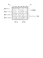
単位期間中の任意のフレームにおける各画素の表示状態に着目すると、上下方向または左右方向に互いに隣接している2個の画素に関して、一方は明表示となっていて、他方は暗表示となっている(図21参照)。ここで、背景部110を灰色表示とし、かつ、ウィンドウ部120を緑色表示とすることを考える。なお、背景部110についての入力階調は「R=64,G=64,B=64」であって、ウィンドウ部120についての入力階調は「R=0,G=192,B=0」であると仮定する。そうすると、或るフレームにおける上記8個の画素に含まれる各絵素の出力階調は、図17に示した階調値変換用ルックアップテーブルに従えば、図23に示すようなものとなる。図23において、例えば符号89で示す絵素については、出力階調は96であって極性はプラスであるということを示している。なお、以下においては、例えば図21における第1列のうちの緑色の絵素の列のことを「列G1」という。
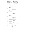
次に、図23および図24を参照しつつ、背景部110への書き込み期間からウィンドウ部120への書き込み期間へと移行する際におけるソース電圧の変化について説明する。なお、ここではゲートバスラインは1行おきに選択されるものと仮定する。従って、第Nラインへの書き込みが行われた水平走査期間の次の水平走査期間には、第N+2ラインへの書き込みが行われる。図24には、列R1,列G1,列B1,列R2,列G2,列B2にそれぞれ対応して設けられているソースバスラインSLの電圧(ソース電圧)およびCSバスラインCSLの電圧の変化を示している。なお、図24では、第N+2ラインへの書き込みが開始される時点を符号t0で示している。列R1については、階調値96に相当するプラス極性用の電圧から階調値0に相当するプラス極性用の電圧へと変化する。列G1については、階調値96に相当するマイナス極性用の電圧から階調値240に相当するマイナス極性用の電圧へと変化する。列B1については、列R1と同様である。列R2については、階調値8に相当するマイナス極性用の電圧から階調値0に相当するマイナス極性用の電圧へと変化する。列G2については、階調値8に相当するプラス極性用の電圧から階調値32に相当するプラス極性用の電圧へと変化する。列B2については、列R2と同様である。以上のことから把握されるように、背景部110への書き込み期間からウィンドウ部120への書き込み期間へと移行する際、全体的にソース電圧はマイナス方向へと変化している。
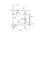
ところで、1つの絵素を形成する絵素部は、図25に示すように、ゲートバスラインGLと、ソースバスラインSLと、共通電極ECと、CSバスラインCSLと、ゲートバスラインGLにゲート電極が接続されるとともにソースバスラインSLにソース電極が接続された薄膜トランジスタ(TFT)101と、その薄膜トランジスタ101のドレイン電極に接続された画素電極102と、画素電極102と共通電極ECとによって形成される液晶容量103と、画素電極102とCSバスラインCSLとによって形成される補助容量104とによって構成されている。このような構成において、ソースバスラインSLとCSバスラインCSLとの間には、図25で符号C9で示すように寄生容量が形成される。また、上述したように、背景部110への書き込み期間からウィンドウ部120への書き込み期間へと移行する際(図24の時点t0)には、全体的にソース電圧はマイナス方向へと変化する。以上より、時点t0には、ソースバスラインSL-CSバスラインCSL間の寄生容量C9の存在に起因して、図24で符号90で示すように、CSバスラインCSLの電圧にマイナス方向のリップル(以下、「CSリップル」という。)が生じる。
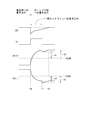
時点t0以降、CSリップルは減衰する、すなわち、CSリップルの大きさは徐々に小さくなる。しかし、図26に示すように第N+2ラインへの書き込み期間が終了する時点t1までにCSリップルの大きさが充分に小さくなっていなければ、時点t1にはゲートバスラインGLが非選択状態となることにより薄膜トランジスタ101(図25参照)がオフ状態となるので、時点t1以降にはCSバスラインCSLの電圧の変化に伴って画素電極電圧(図26のVD(+),VD(-))も変化する。図26に示す例では、時点t1から時点t2までの期間にCSバスラインCSLの電圧が上昇しているので、当該期間中、画素電極電圧も上昇している。このため、極性がプラスにされるべき絵素部では、本来的には符号91で示す大きさの電圧が液晶層に印加されるべきであるにもかかわらず、符号92で示す大きさの電圧が液晶層に印加される。また、極性がマイナスにされるべき絵素部では、本来的には符号93で示す大きさの電圧が液晶層に印加されるべきであるにもかかわらず、符号94で示す大きさの電圧が液晶層に印加される。
また、この液晶表示装置では、ウィンドウ部120への書き込み期間から背景部110への書き込み期間へと移行する際には、全体的にソース電圧はプラス方向へと変化する。このため、図27に示すように、背景部110への書き込み期間が開始する時点t10にはプラス方向のCSリップルが生じる。このCSリップルに起因して、極性がプラスにされるべき絵素部では、本来的には符号95で示す大きさの電圧が液晶層に印加されるべきであるにもかかわらず、符号96で示す大きさの電圧が液晶層に印加される。また、極性がマイナスにされるべき絵素部では、本来的には符号97で示す大きさの電圧が液晶層に印加されるべきであるにもかかわらず、符号98で示す大きさの電圧が液晶層に印加される。
以上のように、背景部110への書き込み期間からウィンドウ部120への書き込み期間へと移行した際やウィンドウ部120への書き込み期間から背景部110への書き込み期間へと移行した際に、本来的に液晶層に印加されるべき電圧とは異なる電圧が液晶層に印加される。その結果、図28に示すような横筋が画面上に現れる。
そこで本発明は、視野角特性を改善するために時間分割方式を採用している液晶表示装置において、画面上への横筋の発生を抑制することを目的とする。
本発明の第1の局面は、映像信号を伝達するための複数の映像信号線と、前記複数の映像信号線と交差するように配設され1水平走査期間ずつ選択される複数の走査信号線と、前記複数の映像信号線と前記複数の走査信号線との交差点にそれぞれ対応するように設けられた複数の画素電極と、前記複数の画素電極との間に補助容量を形成するために前記複数の映像信号線と交差するように配設された複数の補助容量配線とを含む表示部を備え、階調値を示す入力信号に基づいて決定される電圧が前記画素電極に与えられるように前記映像信号を前記複数の映像信号線に印加することによって前記入力信号に基づく画像を前記表示部に表示する液晶表示装置であって、
前記入力信号に含まれる1水平走査期間分のデータであるラインデータ毎に該ラインデータに基づいて決定される第1出力階調に補正を施して、前記複数の映像信号線に印加すべき映像信号電圧に対応する第2出力階調を求める出力階調補正処理部を備え、
前記第2出力階調を求める処理が行われているラインデータに基づいて前記複数の映像信号線に前記映像信号が印加されるべき水平走査期間を処理対象水平走査期間と定義し、前記処理対象水平走査期間の1水平走査期間前の水平走査期間を先行水平走査期間と定義し、前記複数の映像信号線についての前記先行水平走査期間用のラインデータに基づいて求められた第2出力階調に対応する映像信号電圧と前記処理対象水平走査期間用のラインデータに基づいて決定される第1出力階調に対応する映像信号電圧との差の総和を電圧差総和と定義したとき、前記出力階調補正処理部は、前記電圧差総和に基づいて、前記第1出力階調に補正を施して前記第2出力階調を求めることを特徴とする。
前記入力信号に含まれる1水平走査期間分のデータであるラインデータ毎に該ラインデータに基づいて決定される第1出力階調に補正を施して、前記複数の映像信号線に印加すべき映像信号電圧に対応する第2出力階調を求める出力階調補正処理部を備え、
前記第2出力階調を求める処理が行われているラインデータに基づいて前記複数の映像信号線に前記映像信号が印加されるべき水平走査期間を処理対象水平走査期間と定義し、前記処理対象水平走査期間の1水平走査期間前の水平走査期間を先行水平走査期間と定義し、前記複数の映像信号線についての前記先行水平走査期間用のラインデータに基づいて求められた第2出力階調に対応する映像信号電圧と前記処理対象水平走査期間用のラインデータに基づいて決定される第1出力階調に対応する映像信号電圧との差の総和を電圧差総和と定義したとき、前記出力階調補正処理部は、前記電圧差総和に基づいて、前記第1出力階調に補正を施して前記第2出力階調を求めることを特徴とする。
本発明の第2の局面は、本発明の第1の局面において、
前記出力階調補正処理部は、
前記ラインデータのうち前記処理対象水平走査期間に正極性の電圧が印加されるべき画素電極に対応するデータについては、前記電圧差総和が正の値であれば、前記第2出力階調を前記第1出力階調以上の値とし、前記電圧差総和が負の値であれば、前記第2出力階調を前記第1出力階調以下の値とし、
前記ラインデータのうち前記処理対象水平走査期間に負極性の電圧が印加されるべき画素電極に対応するデータについては、前記電圧差総和が正の値であれば、前記第2出力階調を前記第1出力階調以下の値とし、前記電圧差総和が負の値であれば、前記第2出力階調を前記第1出力階調以上の値とすることを特徴とする。
前記出力階調補正処理部は、
前記ラインデータのうち前記処理対象水平走査期間に正極性の電圧が印加されるべき画素電極に対応するデータについては、前記電圧差総和が正の値であれば、前記第2出力階調を前記第1出力階調以上の値とし、前記電圧差総和が負の値であれば、前記第2出力階調を前記第1出力階調以下の値とし、
前記ラインデータのうち前記処理対象水平走査期間に負極性の電圧が印加されるべき画素電極に対応するデータについては、前記電圧差総和が正の値であれば、前記第2出力階調を前記第1出力階調以下の値とし、前記電圧差総和が負の値であれば、前記第2出力階調を前記第1出力階調以上の値とすることを特徴とする。
本発明の第3の局面は、本発明の第2の局面において、
前記第1出力階調の値が等しい複数のデータが存在するとき、前記出力階調補正処理部は、該複数のデータについて、前記電圧差総和の絶対値が大きいほど、前記第1出力階調と前記第2出力階調との差を大きくすることを特徴とする。
前記第1出力階調の値が等しい複数のデータが存在するとき、前記出力階調補正処理部は、該複数のデータについて、前記電圧差総和の絶対値が大きいほど、前記第1出力階調と前記第2出力階調との差を大きくすることを特徴とする。
本発明の第4の局面は、本発明の第1の局面において、
前記画素電極に印加されるべき電圧の極性別に、前記電圧差総和に相当する値と前記第1出力階調との組み合わせと前記第1出力階調の補正に用いるための値である補正用加減算値との対応関係を格納する出力階調補正用ルックアップテーブルを更に備え、
前記出力階調補正処理部は、前記電圧差総和に相当する値と前記第1出力階調との組み合わせに基づいて前記出力階調補正用ルックアップテーブルより取得した補正用加減算値と前記第1出力階調との加減算処理で得られる値を前記第2出力階調とすることを特徴とする。
前記画素電極に印加されるべき電圧の極性別に、前記電圧差総和に相当する値と前記第1出力階調との組み合わせと前記第1出力階調の補正に用いるための値である補正用加減算値との対応関係を格納する出力階調補正用ルックアップテーブルを更に備え、
前記出力階調補正処理部は、前記電圧差総和に相当する値と前記第1出力階調との組み合わせに基づいて前記出力階調補正用ルックアップテーブルより取得した補正用加減算値と前記第1出力階調との加減算処理で得られる値を前記第2出力階調とすることを特徴とする。
本発明の第5の局面は、本発明の第4の局面において、
前記出力階調補正処理部は、前記補正用加減算値と前記第1出力階調との加減算処理を行う前に、前記表示部内の位置に応じて予め定められている倍率を前記補正用加減算値に乗ずることを特徴とする。
前記出力階調補正処理部は、前記補正用加減算値と前記第1出力階調との加減算処理を行う前に、前記表示部内の位置に応じて予め定められている倍率を前記補正用加減算値に乗ずることを特徴とする。
本発明の第6の局面は、本発明の第5の局面において、
前記表示部内の位置と前記補正用加減算値の補正に用いるための倍率との対応関係を格納する倍率ルックアップテーブルを更に備え、
前記出力階調補正処理部は、各データについての前記表示部内の位置に基づいて前記倍率ルックアップテーブルより取得した倍率を前記補正用加減算値に乗ずることを特徴とする。
前記表示部内の位置と前記補正用加減算値の補正に用いるための倍率との対応関係を格納する倍率ルックアップテーブルを更に備え、
前記出力階調補正処理部は、各データについての前記表示部内の位置に基づいて前記倍率ルックアップテーブルより取得した倍率を前記補正用加減算値に乗ずることを特徴とする。
本発明の第7の局面は、本発明の第1の局面において、
前記入力信号に含まれる各データが示す階調値に基づいて、前記第1出力階調として、比較的明るい表示を行うための明表示用第1出力階調と比較的暗い表示を行うための暗表示用第1出力階調とを求める階調値取得部を更に備え、
1画面分の画像は複数のフレーム期間をかけて表示され、
前記入力信号に含まれる各データに着目したとき、前記複数のフレーム期間のうちの半分のフレーム期間には、前記明表示用第1出力階調に補正が施されることにより求められた第2出力階調に対応する映像信号電圧が当該各データに対応する画素電極に印加され、前記複数のフレーム期間のうちの残りの半分のフレーム期間には、前記暗表示用第1出力階調に補正が施されることにより求められた第2出力階調に対応する映像信号電圧が当該各データに対応する画素電極に印加されることを特徴とする。
前記入力信号に含まれる各データが示す階調値に基づいて、前記第1出力階調として、比較的明るい表示を行うための明表示用第1出力階調と比較的暗い表示を行うための暗表示用第1出力階調とを求める階調値取得部を更に備え、
1画面分の画像は複数のフレーム期間をかけて表示され、
前記入力信号に含まれる各データに着目したとき、前記複数のフレーム期間のうちの半分のフレーム期間には、前記明表示用第1出力階調に補正が施されることにより求められた第2出力階調に対応する映像信号電圧が当該各データに対応する画素電極に印加され、前記複数のフレーム期間のうちの残りの半分のフレーム期間には、前記暗表示用第1出力階調に補正が施されることにより求められた第2出力階調に対応する映像信号電圧が当該各データに対応する画素電極に印加されることを特徴とする。
本発明の第8の局面は、本発明の第1の局面において、
前記表示部は、一定の階調値に基づく画像の表示が行われる第1表示部と前記第1表示部以外の領域であって任意の階調に基づく画像の表示が行われる第2表示部とからなることを特徴とする。
前記表示部は、一定の階調値に基づく画像の表示が行われる第1表示部と前記第1表示部以外の領域であって任意の階調に基づく画像の表示が行われる第2表示部とからなることを特徴とする。
本発明の第9の局面は、映像信号を伝達するための複数の映像信号線と、前記複数の映像信号線と交差するように配設され1水平走査期間ずつ選択される複数の走査信号線と、前記複数の映像信号線と前記複数の走査信号線との交差点にそれぞれ対応するように設けられた複数の画素電極と、前記複数の画素電極との間に補助容量を形成するために前記複数の映像信号線と交差するように配設された複数の補助容量配線とを含む表示部を備え、階調値を示す入力信号に基づいて決定される電圧が前記画素電極に与えられるように前記映像信号を前記複数の映像信号線に印加することによって前記入力信号に基づく画像を前記表示部に表示する液晶表示装置の駆動方法であって、
前記入力信号に含まれる1水平走査期間分のデータであるラインデータ毎に該ラインデータに基づいて決定される第1出力階調に補正を施して、前記複数の映像信号線に印加すべき映像信号電圧に対応する第2出力階調を求める出力階調補正ステップを備え、
前記第2出力階調を求める処理が行われているラインデータに基づいて前記複数の映像信号線に前記映像信号が印加されるべき水平走査期間を処理対象水平走査期間と定義し、前記処理対象水平走査期間の1水平走査期間前の水平走査期間を先行水平走査期間と定義したとき、前記出力階調補正ステップは、
前記複数の映像信号線についての前記先行水平走査期間用のラインデータに基づいて求められた第2出力階調に対応する映像信号電圧と前記処理対象水平走査期間用のラインデータに基づいて決定される第1出力階調に対応する映像信号電圧との差の総和を電圧差総和として求める電圧差総和算出ステップと、
前記電圧差総和に基づいて前記第2出力階調を求める第2出力階調算出ステップとを含むことを特徴とする。
前記入力信号に含まれる1水平走査期間分のデータであるラインデータ毎に該ラインデータに基づいて決定される第1出力階調に補正を施して、前記複数の映像信号線に印加すべき映像信号電圧に対応する第2出力階調を求める出力階調補正ステップを備え、
前記第2出力階調を求める処理が行われているラインデータに基づいて前記複数の映像信号線に前記映像信号が印加されるべき水平走査期間を処理対象水平走査期間と定義し、前記処理対象水平走査期間の1水平走査期間前の水平走査期間を先行水平走査期間と定義したとき、前記出力階調補正ステップは、
前記複数の映像信号線についての前記先行水平走査期間用のラインデータに基づいて求められた第2出力階調に対応する映像信号電圧と前記処理対象水平走査期間用のラインデータに基づいて決定される第1出力階調に対応する映像信号電圧との差の総和を電圧差総和として求める電圧差総和算出ステップと、
前記電圧差総和に基づいて前記第2出力階調を求める第2出力階調算出ステップとを含むことを特徴とする。
本発明の第10の局面は、本発明の第9の局面において、
前記第2出力階調算出ステップでは、
前記ラインデータのうち前記処理対象水平走査期間に正極性の電圧が印加されるべき画素電極に対応するデータについては、前記電圧差総和が正の値であれば、前記第2出力階調は前記第1出力階調以上の値とされ、前記電圧差総和が負の値であれば、前記第2出力階調は前記第1出力階調以下の値とされ、
前記ラインデータのうち前記処理対象水平走査期間に負極性の電圧が印加されるべき画素電極に対応するデータについては、前記電圧差総和が正の値であれば、前記第2出力階調は前記第1出力階調以下の値とされ、前記電圧差総和が負の値であれば、前記第2出力階調は前記第1出力階調以上の値とされることを特徴とする。
前記第2出力階調算出ステップでは、
前記ラインデータのうち前記処理対象水平走査期間に正極性の電圧が印加されるべき画素電極に対応するデータについては、前記電圧差総和が正の値であれば、前記第2出力階調は前記第1出力階調以上の値とされ、前記電圧差総和が負の値であれば、前記第2出力階調は前記第1出力階調以下の値とされ、
前記ラインデータのうち前記処理対象水平走査期間に負極性の電圧が印加されるべき画素電極に対応するデータについては、前記電圧差総和が正の値であれば、前記第2出力階調は前記第1出力階調以下の値とされ、前記電圧差総和が負の値であれば、前記第2出力階調は前記第1出力階調以上の値とされることを特徴とする。
本発明の第11の局面は、本発明の第9の局面において、
前記入力信号に含まれる各データが示す階調値に基づいて、前記第1出力階調として、比較的明るい表示を行うための明表示用第1出力階調と比較的暗い表示を行うための暗表示用第1出力階調とを求める階調値取得ステップを更に備え、
1画面分の画像は複数のフレーム期間をかけて表示され、
前記入力信号に含まれる各データに着目したとき、前記複数のフレーム期間のうちの半分のフレーム期間には、前記明表示用第1出力階調に補正が施されることにより求められた第2出力階調に対応する映像信号電圧が当該各データに対応する画素電極に印加され、前記複数のフレーム期間のうちの残りの半分のフレーム期間には、前記暗表示用第1出力階調に補正が施されることにより求められた第2出力階調に対応する映像信号電圧が当該各データに対応する画素電極に印加されることを特徴とする。
前記入力信号に含まれる各データが示す階調値に基づいて、前記第1出力階調として、比較的明るい表示を行うための明表示用第1出力階調と比較的暗い表示を行うための暗表示用第1出力階調とを求める階調値取得ステップを更に備え、
1画面分の画像は複数のフレーム期間をかけて表示され、
前記入力信号に含まれる各データに着目したとき、前記複数のフレーム期間のうちの半分のフレーム期間には、前記明表示用第1出力階調に補正が施されることにより求められた第2出力階調に対応する映像信号電圧が当該各データに対応する画素電極に印加され、前記複数のフレーム期間のうちの残りの半分のフレーム期間には、前記暗表示用第1出力階調に補正が施されることにより求められた第2出力階調に対応する映像信号電圧が当該各データに対応する画素電極に印加されることを特徴とする。
本発明の第1の局面によれば、入力信号に基づいて得られる階調値(第1出力階調)に対して補正が施されることによって、映像信号電圧を決定するための階調値(第2出力階調)が求められる。詳しくは、補正をしなかったと仮定した場合における連続する2水平走査期間の間での全ての映像信号線についての映像信号電圧の変化の総和(電圧差総和)に基づいて第1出力階調に補正が施されて第2出力階調が求められる。ここで、連続する2水平走査期間の間での全ての映像信号線についての映像信号電圧の変化の総和は、補助容量配線に生じるリップル(CSリップル)の大きさに比例している。従って、上記のように電圧差総和を考慮して補正が施されることにより、CSリップルに起因して各ラインへの書き込み期間終了後に画素電極電圧に変化が生じても、変化後の画素電極電圧が本来画素電極に印加すべき電圧に近い電圧となるようにすることが可能となる。このため、階調値を好適に補正することにより、映像信号電圧の変化に偏りがある場合に従来生じていた画面上への横筋の発生が抑制される。
本発明の第2の局面によれば、CSリップルに起因する画素電極電圧の変化方向を予め考慮して、第1出力階調に補正が施されて第2出力階調が求められる。このため、画面上への横筋の発生が、より効果的に抑制される。
本発明の第3の局面によれば、補正をしなかった場合に生じると予測されるCSリップルの大きさが大きいほど第1出力階調に大きな補正が施されて第2出力階調が求められる。このため、画面上への横筋の発生が、さらに効果的に抑制される。
本発明の第4の局面によれば、「電圧差総和に相当する値と第1出力階調との組み合わせ」と「第1出力階調の補正に用いるための値である補正用加減算値」との対応関係をルックアップテーブルに格納する構成とすることにより、回路の複雑化が防止される。
本発明の第5の局面によれば、表示部内の位置に応じて定められた倍率が、第2出力階調を求めるための補正用加減算値に乗ぜられる。このため、表示部内の位置によるCSリップルの減衰のスピードの違いを考慮しつつ、第2出力階調が求められる。これにより、全てのラインにおいて、より効果的に、CSリップルに起因して従来生じていた画面上への横筋の発生が抑制される。
本発明の第6の局面によれば、表示部内の位置と倍率との対応関係をルックアップテーブルに格納する構成とすることにより、回路の複雑化が防止される。
時間分割方式を採用する液晶表示装置においては、連続する2水平走査期間の間での映像信号電圧の変化に偏りが生じやすいので、CSリップルに起因する画面上への横筋が発生しやすい。しかしながら、本発明の第7の局面によれば、時間分割方式を採用する液晶表示装置において、画面上への横筋の発生が効果的に抑制される。
表示部の一部を用いて画像表示が行われる液晶表示装置においては、書き込みラインが例えば背景表示部から画像表示部(あるいは画像表示部から背景表示部)へと切り替わる際に映像信号電圧の変化に偏りが生じやすいので、CSリップルに起因する画面上への横筋が発生しやすい。しかしながら、本発明の第8の局面によれば、表示部の一部を用いて画像表示が行われる液晶表示装置において、画面上への横筋の発生が効果的に抑制される。
本発明の第9の局面によれば、本発明の第1の局面と同様の効果を液晶表示装置の駆動方法において奏することができる。
本発明の第10の局面によれば、本発明の第2の局面と同様の効果を液晶表示装置の駆動方法において奏することができる。
本発明の第11の局面によれば、本発明の第7の局面と同様の効果を液晶表示装置の駆動方法において奏することができる。
以下、添付図面を参照しつつ、本発明の一実施形態について説明する。
<1.全体構成および動作>
図2は、本発明の一実施形態に係るアクティブマトリクス型の液晶表示装置の全体構成を示すブロック図である。図2に示すように、この液晶表示装置は、表示部100とゲートドライバ(走査信号線駆動回路)200とソースドライバ(映像信号線駆動回路)300と補助容量配線ドライバ400と表示制御回路500とを備えている。
図2は、本発明の一実施形態に係るアクティブマトリクス型の液晶表示装置の全体構成を示すブロック図である。図2に示すように、この液晶表示装置は、表示部100とゲートドライバ(走査信号線駆動回路)200とソースドライバ(映像信号線駆動回路)300と補助容量配線ドライバ400と表示制御回路500とを備えている。
表示部100には、複数本(i本)のゲートバスライン(走査信号線)GL1~GLiと、複数本(j本)のソースバスライン(映像信号線)SL1~SLjと、ゲートバスラインGL1~GLiとソースバスラインSL1~SLjとの交差点にそれぞれ対応して設けられた複数個(i×j個)の絵素部とが形成されている。上記複数個の絵素部はマトリクス状に配置されて画素アレイを構成している。
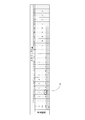
表示部100には、また、ゲートバスラインGL1~GLiと1対1で対応するように、図3に示すように複数本(i本)のCSバスライン(補助容量配線)CSL1~CSLiが形成されている。各CSバスラインは、ゲートバスラインと平行に延びるように配設されている。パネル基板10上の表示部100外の領域には、CSバスラインCSL1~CSLiに所望の電圧を与えるための構成要素として、CS幹線11が配設されている。各CSバスラインは、表示部100の両端近傍において、CS幹線11に接続されている。また、CS幹線11は、補助容量配線ドライバ400に接続されている。以上より、CSバスラインCSL1~CSLiと補助容量配線ドライバ400とがCS幹線11を介して接続されている。
図25は、絵素部の構成を示す回路図である。図25に示すように、各絵素部は、ゲートバスラインGLと、ソースバスラインSLと、共通電極ECと、CSバスラインCSLと、ゲートバスラインGLにゲート電極が接続されるとともにソースバスラインSLにソース電極が接続された薄膜トランジスタ(TFT)101と、その薄膜トランジスタ101のドレイン電極に接続された画素電極102と、画素電極102と共通電極ECとによって形成される液晶容量103と、画素電極102とCSバスラインCSLとによって形成される補助容量104とによって構成されている。また、液晶容量103と補助容量104とによって画素容量が形成されている。このような構成において、薄膜トランジスタ101のゲート電極がゲートバスラインGLからアクティブな走査信号を受けたときに当該薄膜トランジスタ101のソース電極がソースバスラインSLから受ける映像信号に基づいて、画素容量に画素値を示す電圧が保持される。
ところで、本実施形態に係る液晶表示装置においては、視野角特性を改善するための技術として、時間分割方式が採用されている。1画面分の画像を表示する単位期間は、4つのフレームで構成されている(図14および図18を参照)。また、この液晶表示装置の動作中には、図19に示すように、表示部100の中央部に画像を表示するためのウィンドウ部120が設けられ、そのウィンドウ部120の周囲に背景色を表示するための背景部110が設けられる。また、赤色(R),緑色(G),および青色(B)の3つの絵素によって1つの画素が構成されているものとする。なお、本実施形態においては、背景部110によって第1表示部が実現され、ウィンドウ部120によって第2表示部が実現されている。
次に、図2に示す構成要素の動作について説明する。表示制御回路500は、外部から送られる画像信号DATおよび水平同期信号や垂直同期信号などのタイミング信号群TGを受け取り、デジタル映像信号DVと、ゲートドライバ200の動作を制御するためのゲートスタートパルス信号GSPおよびゲートクロック信号GCKと、ソースドライバ300の動作を制御するためのソーススタートパルス信号SSP,ソースクロック信号SCK,およびラッチストローブ信号LSと、補助容量配線ドライバ400の動作を制御するためのCSバスライン制御信号SCSとを出力する。
ゲートドライバ200は、表示制御回路500から出力されるゲートスタートパルス信号GSPおよびゲートクロック信号GCKを受け取り、各ゲートバスラインに走査信号を印加する。なお、本実施形態においては、ゲートドライバ200はゲートバスラインを1行おきに選択する。すなわち、「1ライン目、3ライン目、・・・、i-3ライン目、i-1ライン目、2ライン目、4ライン目、・・・、i-2ライン目、iライン目」という順序で各ゲートバスラインが選択状態となる。ソースドライバ300は、表示制御回路500から出力されるデジタル映像信号DV,ソーススタートパルス信号SSP,ソースクロック信号SCK,およびラッチストローブ信号LSを受け取り、各ソースバスラインに駆動用映像信号を印加する。補助容量配線ドライバ400は、表示制御回路500から出力されるCSバスライン制御信号SCSに基づいて、CSバスラインCSLに印加する電圧を制御する。
以上のようにして、CSバスラインCSLに印加される電圧の制御が行われつつ、各ゲートバスラインGLに走査信号が印加され、各ソースバスラインSLに駆動用映像信号が印加されることにより、外部から送られた画像信号DATに基づく画像が表示部100に表示される。
<2.表示制御回路の構成>
図4は、本実施形態における表示制御回路500の構成を示すブロック図である。表示制御回路500には、インタフェース部51と階調値取得部52と横筋補正処理部53とタイミングジェネレータ54とが含まれている。階調値取得部52には、階調値変換用ルックアップテーブル521が含まれている。横筋補正処理部53には、CSリップル見積もり部531と階調値-電圧変換ルックアップテーブル532と階調値補正部533とプラス極性背景用ルックアップテーブル534とマイナス極性背景用ルックアップテーブル535とが含まれている。
図4は、本実施形態における表示制御回路500の構成を示すブロック図である。表示制御回路500には、インタフェース部51と階調値取得部52と横筋補正処理部53とタイミングジェネレータ54とが含まれている。階調値取得部52には、階調値変換用ルックアップテーブル521が含まれている。横筋補正処理部53には、CSリップル見積もり部531と階調値-電圧変換ルックアップテーブル532と階調値補正部533とプラス極性背景用ルックアップテーブル534とマイナス極性背景用ルックアップテーブル535とが含まれている。
インタフェース部51は、画像信号DATおよびタイミング信号群TGを外部から受け取り、それらを適宜階調値取得部52およびタイミングジェネレータ54に与える。階調値取得部52は、階調値変換用ルックアップテーブル521を参照して、画像信号DATの示す階調である入力階調に基づき、明画素用の出力階調(明表示用第1出力階調)および暗画素用の出力階調(暗表示用第1出力階調)を取得する。なお、上述したように、階調値変換用ルックアップテーブル521には、入力階調と明画素および暗画素の出力階調とを対応付けたデータが格納されている(図17参照)。
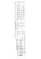
横筋補正処理部53は、CSリップルに起因する画面上への横筋の発生を抑制するために、階調値取得部52によって取得された階調値(すなわち、階調値変換用ルックアップテーブル521より取得された出力階調)に補正を施し、補正後の階調値をデジタル映像信号DVとして出力する。なお、以下においては、階調値取得部52によって取得された階調値を「第1出力階調」といい、横筋補正処理部53による補正処理によって求められる階調値を「第2出力階調」という。階調値-電圧変換ルックアップテーブル532には、階調値とソース電圧とを対応付けたデータが格納されている。図5は、階調値-電圧変換ルックアップテーブル532の一構成例を示す図である。例えば、符号71の矢印で示す行は「階調値が10であれば、極性がプラスにされるべき絵素部での書き込みのためにはソース電圧を9.11Vとし、極性がマイナスにされるべき絵素部での書き込みのためにはソース電圧を5.33Vとする。」ということを示している。CSリップル見積もり部531は、階調値-電圧変換ルックアップテーブル532を参照しつつ、各CSバスラインCSLに生じるCSリップルの大きさを見積もる。以下、CSリップルの大きさを数値で表したものを「CSリップル量」という。
プラス極性背景用ルックアップテーブル534およびマイナス極性背景用ルックアップテーブル535には、「CSリップル量と背景階調との組み合わせ」と「補正用加減算値」とを対応付けたデータが格納されている。なお、補正用加減算値とは、後述する横筋補正処理において第2出力階調を求めるための演算処理で用いられる値である。図6は、プラス極性背景用ルックアップテーブル534の一構成例を示す図である。図7は、マイナス極性背景用ルックアップテーブルの一構成例を示す図である。例えば、図6で符号72で示すデータは「CSリップル量が-7925であれば、背景階調が696の絵素については、補正用加減算値を-83とする。」ということを示している。階調値補正部533は、CSリップル見積もり部531が見積もったCSリップル量に基づいてプラス極性背景用ルックアップテーブル534およびマイナス極性背景用ルックアップテーブル535を参照して補正用加減算値を求め、当該補正用加減算値を用いて各絵素についての第2出力階調を求める。なお、CSリップル見積もり部531および階調値補正部533によって行われる詳しい処理内容については後述する。また、以下においては、プラス極性背景用ルックアップテーブル534とマイナス極性背景用ルックアップテーブル535とを合わせて「極性別背景用ルックアップテーブル」ともいう。
タイミングジェネレータ54は、上述のソーススタートパルス信号SSP,ソースクロック信号SCK,ラッチストローブ信号LS,ゲートスタートパルス信号GSP,ゲートクロック信号GCK,およびCSバスライン制御信号SCSを生成して、それらを出力する。
なお、本実施形態においては、横筋補正処理部53によって出力階調補正処理部が実現され、プラス極性背景用ルックアップテーブル534およびマイナス極性背景用ルックアップテーブル535によって出力階調補正用ルックアップテーブルが実現されている。
<3.横筋補正処理>
次に、CSリップルに起因する画面上への横筋の発生を抑制するための処理である横筋補正処理について説明する。図1は、本実施形態における横筋補正処理の手順を示すフローチャートである。なお、この横筋補正処理は上述した横筋補正処理部53によって行われる。また、図1には1ライン分についての手順を示しており、液晶表示装置の動作中、ステップS110からステップS130までの処理が繰り返される。
次に、CSリップルに起因する画面上への横筋の発生を抑制するための処理である横筋補正処理について説明する。図1は、本実施形態における横筋補正処理の手順を示すフローチャートである。なお、この横筋補正処理は上述した横筋補正処理部53によって行われる。また、図1には1ライン分についての手順を示しており、液晶表示装置の動作中、ステップS110からステップS130までの処理が繰り返される。
階調値取得部52によって1ライン分のデータ(ラインデータ)についての第1出力階調が取得されると、CSリップル見積もり部531によって、第1出力階調の取得が行われたライン(処理対象ライン)に対応して設けられているCSバスラインCSLに生じるCSリップルの大きさ(CSリップル量)の見積もりが行われる(ステップS110)。詳しくは、CSリップル見積もり部531は、まず、各ソースバスラインSLについて、「処理対象ラインが選択状態となる水平走査期間の1水平走査期間前におけるソース電圧」と「階調値取得部52によって取得された第1出力階調に基づいて求められるソース電圧」との差(以下、「ソース電圧変化量」という。)を求める。その際、CSリップル見積もり部531は、階調値取得部52によって取得された第1出力階調をソース電圧に変換するために、図5に示したような階調値-電圧変換ルックアップテーブル532を参照する。そして、CSリップル見積もり部531は、全てのソースバスラインSLについてのソース電圧変化量の総和を求める。以下、ソース電圧変化量の総和のことを「1ライン分ソース電圧変化量」という。なお、処理対象ラインが選択状態となる水平走査期間が処理対象水平走査期間に相当し、処理対象水平走査期間の1水平走査期間前の水平走査期間が先行水平走査期間に相当する。また、1ライン分ソース電圧変化量が電圧差総和に相当する。
例えば、水平方向に1920個の画素が存在する液晶表示装置においてMライン目が処理対象となっている場合、1ライン分ソース電圧変化量は次のように求められる。本実施形態においては1つの画素は3つの絵素で構成され、かつ、ゲートバスラインGLは1行おきに選択状態となるので、5760本のソースバスラインSLについての「M-2ライン目への書き込みが行われる水平走査期間におけるソース電圧」と「Mライン目についての、階調値取得部52によって取得された第1出力階調に基づき階調値-電圧変換ルックアップテーブル532を参照することによって得られるソース電圧」との差の総和が1ライン分ソース電圧変化量として求められる。ここで、ソース電圧の変化量を求めるためにはM-2ライン目のデータについては補正後の電圧を参照することが原理的には正しいので、「M-2ライン目への書き込みが行われる水平走査期間におけるソース電圧」とは第2階調に基づく電圧である。なお、1ライン分ソース電圧変化量がプラスの値であれば、処理対象ラインへの書き込みが行われることによって、CSバスラインCSLの電圧が上昇するようにCSリップルが生じることになる。一方、1ライン分ソース電圧変化量がマイナスの値であれば、処理対象ラインへの書き込みが行われることによって、CSバスラインCSLの電圧が低下するようにCSリップルが生じることになる。
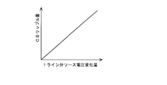
ところで、CSリップル量と1ライン分ソース電圧変化量とは図8に示すような比例関係にある。従って、1ライン分ソース電圧変化量に基づいて、CSバスラインCSLに生じることが予測されるCSリップル量を見積もることができる。そこで、本実施形態においては、CSリップル見積もり部531は、上述のようにして求めた1ライン分ソース電圧変化量よりCSリップル量を見積もっている。以上のように、ステップS110では、CSリップル見積もり部531によるCSリップル量の見積もりが行われる。
次に、階調値補正部533によって、ステップS110で求められたCSリップル量に基づき、処理対象ラインに含まれる各絵素について、極性別背景用ルックアップテーブルより補正用加減算値が取得される(ステップS120)。補正用加減算値の取得の際、極性がプラスにされるべき絵素については、プラス極性背景用ルックアップテーブル534が参照され、極性がマイナスにされるべき絵素については、マイナス極性背景用ルックアップテーブル535が参照される。以上のように、ステップS120では、階調値補正部533による各絵素についての補正用加減算値の取得が行われる。
次に、階調値補正部533によって、第2出力階調の算出が行われる(ステップS130)。詳しくは、階調値補正部533は、処理対象ラインに含まれる各絵素について、階調値取得部52によって取得された階調値(第1出力階調)とステップS120で取得された補正用加減算値とに基づいて、第2出力階調を算出する。例えば、階調値取得部52によって取得された階調値が15であって、ステップS120で取得された補正用加減算値が3であれば、第2出力階調は18となる。また、例えば、階調値取得部52によって取得された階調値が696であって、ステップS120で取得された補正用加減算値が-55であれば、第2出力階調は641となる。以上のように、ステップS130では、階調値補正部533による各絵素についての第2出力階調の算出が行われる。このようにして第2出力階調が算出されることによって、横筋補正処理は終了する。この横筋補正処理で求められた第2出力階調が、上述したように、デジタル映像信号DVとして表示制御回路500から出力される。
なお、図6および図7で示した極性別背景用ルックアップテーブル(プラス極性背景用ルックアップテーブル534およびマイナス極性背景用ルックアップテーブル535)ではCSリップル量を横軸としているが、1ライン分ソース電圧変化量を横軸としても良い。上述したようにCSリップル量と1ライン分ソース電圧変化量とは比例関係にあるので、1ライン分ソース電圧変化量に相当する値を極性別背景用ルックアップテーブルの横軸とすることができる。
<4.効果>
本実施形態によれば、視野角特性を改善するために時間分割方式を採用している液晶表示装置において、入力信号(画像信号DAT)に基づいて明画素用および暗画素用の階調値(第1出力階調)が取得された後、それら明画素用および暗画素用の階調値に対して次のように補正が施されることによって、処理対象ラインに含まれる絵素部での書き込み用のソース電圧を決定するための階調値(第2出力階調)が求められる。まず、補正が施されなかったと仮定した場合に処理対象ラインへの書き込みの際にCSバスラインCSLに生ずることが予測されるCSリップルの大きさ(CSリップル量)が見積もられる。CSリップル量の見積もりは、全ソースバスラインSLについての「処理対象ラインへの書き込みが行われる水平走査期間の1水平走査期間前におけるソース電圧」と「入力信号に基づく出力階調に対応するソース電圧」との差を全て加算することによって行われる。そして、CSリップル量の大きさに応じて、極性別背景用ルックアップテーブルに格納されている補正用加減算値を用いて出力階調に補正が施される。ここで、極性別背景用ルックアップテーブルには、次のようにデータが格納されている。
(1)CSリップル量(絶対値)が大きいほど補正用加減算値(絶対値)を大きくする。
(2)CSリップルに起因する画素電極電圧の変化が打ち消されるように、具体的には(2-1)および(2-2)のように、補正用加減算値の正負が決められている。
(2-1)極性がプラスにされるべき絵素については、CSリップル量がプラスの値であれば補正用加減算値をプラスの値とし、CSリップル量がマイナスの値であれば補正用加減算値をマイナスの値とする。
(2-2)極性がマイナスにされるべき絵素については、CSリップル量がプラスの値であれば補正用加減算値をマイナスの値とし、CSリップル量がマイナスの値であれば補正用加減算値をプラスの値とする。
(3)VTカーブ(図15参照)の立ち上がり(変曲点)近傍に相当する背景階調についての補正用加減算値(絶対値)を比較的大きくする。
以上より、1ライン分ソース電圧変化量およびそれに基づく画素電極電圧の変化方向を考慮して出力階調に補正が施されることにより、各絵素部においてCSリップルに起因する画素電極電圧の変化が打ち消されるように、各絵素部に対応するソースバスラインSLに駆動用映像信号が印加される。このため、背景部110への書き込み期間からウィンドウ部120への書き込み期間(あるいは、ウィンドウ部120への書き込み期間から背景部110への書き込み期間)へと移行する時のように出力階調の変化が比較的大きい時でも、各絵素部において画素電極電圧は本来的に画素電極に印加されるべき電圧に近い電圧となる。その結果、極性がプラスにされるべき絵素部においても極性がマイナスにされるべき絵素部においても、本来的に液晶層に印加されるべき大きさの電圧(図9で符号73で示す大きさの電圧)が液晶層に印加される。以上より、時間分割方式を採用している液晶表示装置において従来生じていた画面上への横筋の発生が抑制される。
本実施形態によれば、視野角特性を改善するために時間分割方式を採用している液晶表示装置において、入力信号(画像信号DAT)に基づいて明画素用および暗画素用の階調値(第1出力階調)が取得された後、それら明画素用および暗画素用の階調値に対して次のように補正が施されることによって、処理対象ラインに含まれる絵素部での書き込み用のソース電圧を決定するための階調値(第2出力階調)が求められる。まず、補正が施されなかったと仮定した場合に処理対象ラインへの書き込みの際にCSバスラインCSLに生ずることが予測されるCSリップルの大きさ(CSリップル量)が見積もられる。CSリップル量の見積もりは、全ソースバスラインSLについての「処理対象ラインへの書き込みが行われる水平走査期間の1水平走査期間前におけるソース電圧」と「入力信号に基づく出力階調に対応するソース電圧」との差を全て加算することによって行われる。そして、CSリップル量の大きさに応じて、極性別背景用ルックアップテーブルに格納されている補正用加減算値を用いて出力階調に補正が施される。ここで、極性別背景用ルックアップテーブルには、次のようにデータが格納されている。
(1)CSリップル量(絶対値)が大きいほど補正用加減算値(絶対値)を大きくする。
(2)CSリップルに起因する画素電極電圧の変化が打ち消されるように、具体的には(2-1)および(2-2)のように、補正用加減算値の正負が決められている。
(2-1)極性がプラスにされるべき絵素については、CSリップル量がプラスの値であれば補正用加減算値をプラスの値とし、CSリップル量がマイナスの値であれば補正用加減算値をマイナスの値とする。
(2-2)極性がマイナスにされるべき絵素については、CSリップル量がプラスの値であれば補正用加減算値をマイナスの値とし、CSリップル量がマイナスの値であれば補正用加減算値をプラスの値とする。
(3)VTカーブ(図15参照)の立ち上がり(変曲点)近傍に相当する背景階調についての補正用加減算値(絶対値)を比較的大きくする。
以上より、1ライン分ソース電圧変化量およびそれに基づく画素電極電圧の変化方向を考慮して出力階調に補正が施されることにより、各絵素部においてCSリップルに起因する画素電極電圧の変化が打ち消されるように、各絵素部に対応するソースバスラインSLに駆動用映像信号が印加される。このため、背景部110への書き込み期間からウィンドウ部120への書き込み期間(あるいは、ウィンドウ部120への書き込み期間から背景部110への書き込み期間)へと移行する時のように出力階調の変化が比較的大きい時でも、各絵素部において画素電極電圧は本来的に画素電極に印加されるべき電圧に近い電圧となる。その結果、極性がプラスにされるべき絵素部においても極性がマイナスにされるべき絵素部においても、本来的に液晶層に印加されるべき大きさの電圧(図9で符号73で示す大きさの電圧)が液晶層に印加される。以上より、時間分割方式を採用している液晶表示装置において従来生じていた画面上への横筋の発生が抑制される。
<5.変形例>
以下、上記実施形態の変形例について説明する。
以下、上記実施形態の変形例について説明する。
<5.1 第1の変形例>
一般に、各CSバスラインCSL1~CSLiには、表示部100の一方の側に設けられた補助容量配線ドライバ400からCS幹線11を介して所望の電圧が供給される(図3参照)。このような構成のため、表示部100の上方部と表示部100の下方部とでは負荷が異なり、また、同じラインであっても表示部100の中央部と表示部100の端部とでは負荷が異なる。このため、表示部100内の位置によって、CSリップルの減衰のスピードが異なる。その結果、極性別背景用ルックアップテーブルより取得される補正用加減算値を用いて出力階調に補正を施しても、横筋の発生を抑制する効果が小さいことがある。そこで、本変形例においては、横筋補正処理部53内に図10に示すようなルックアップテーブル(以下、「面内分布補正用ルックアップテーブル」という。)を更に備える構成とし、同じようにソース電圧が変化する場合であっても表示部100内の位置によって異なる補正量で出力階調に補正が施されるようにしている。例えば図3に示すようにCSバスラインに与える信号が表示部100の上方部から入力される場合、CSリップル量は、表示部100の上方では比較的小さくなり、表示部100の下方では比較的大きくなる。従って、表示部100の上方では、補正量は小さくて良いので、面内分布補正用ルックアップテーブルの値(補正用倍率)は小さくされ、表示部100の下方では、補正量を大きくしなければならないので面内分布補正用ルックアップテーブルの値(補正用倍率)は大きくされる。なお、面内分布補正用ルックアップテーブルによって倍率ルックアップテーブルが実現されている。
一般に、各CSバスラインCSL1~CSLiには、表示部100の一方の側に設けられた補助容量配線ドライバ400からCS幹線11を介して所望の電圧が供給される(図3参照)。このような構成のため、表示部100の上方部と表示部100の下方部とでは負荷が異なり、また、同じラインであっても表示部100の中央部と表示部100の端部とでは負荷が異なる。このため、表示部100内の位置によって、CSリップルの減衰のスピードが異なる。その結果、極性別背景用ルックアップテーブルより取得される補正用加減算値を用いて出力階調に補正を施しても、横筋の発生を抑制する効果が小さいことがある。そこで、本変形例においては、横筋補正処理部53内に図10に示すようなルックアップテーブル(以下、「面内分布補正用ルックアップテーブル」という。)を更に備える構成とし、同じようにソース電圧が変化する場合であっても表示部100内の位置によって異なる補正量で出力階調に補正が施されるようにしている。例えば図3に示すようにCSバスラインに与える信号が表示部100の上方部から入力される場合、CSリップル量は、表示部100の上方では比較的小さくなり、表示部100の下方では比較的大きくなる。従って、表示部100の上方では、補正量は小さくて良いので、面内分布補正用ルックアップテーブルの値(補正用倍率)は小さくされ、表示部100の下方では、補正量を大きくしなければならないので面内分布補正用ルックアップテーブルの値(補正用倍率)は大きくされる。なお、面内分布補正用ルックアップテーブルによって倍率ルックアップテーブルが実現されている。
図11は、本変形例における横筋補正処理の手順を示すフローチャートである。ステップS210では、上記実施形態におけるステップS110と同様、CSリップル量の見積もりが行われる。次に、ステップS220では、上記実施形態におけるステップS120と同様、補正用加減算値の取得が行われる。さらに、ステップS230では、階調値補正部533によって、処理対象ラインに含まれる各絵素について、面内分布補正用ルックアップテーブルより補正用倍率が取得される。そして、ステップS240では、階調値補正部533によって、ステップS220で取得された補正用加減算値とステップS230で取得された補正用倍率との積が求められる。
その後、ステップS250では、階調値取得部52によって取得された階調値(第1出力階調)とステップS240で求められた値(補正用加減算値と補正用倍率との積)とに基づいて、第2出力階調を算出する。例えば、階調値取得部52によって取得された階調値が15であって、ステップS240で求められた値が2であれば、第2出力階調は17となる。また、例えば、階調値取得部52によって取得された階調値が696であって、ステップS240で求められた値が-35であれば、第2出力階調は661となる。以上のように、ステップS250では、階調値補正部533による各絵素についての第2出力階調の算出が行われる。
本変形例によれば、表示部100内の位置によるCSリップルの減衰のスピードの違いを考慮しつつ、入力信号に基づく出力階調(階調値取得部52によって取得された階調値)に補正が施されて、ソース電圧を決定するための階調値(第2出力階調)が求められる。このため、全てのラインにおいて、より効果的に、CSリップルに起因して従来生じていた画面上への横筋の発生が抑制される。
<5.2 第2の変形例>
上記実施形態においては、1つの画素は3つの絵素で構成されていたが、本発明はこれに限定されない。例えば、黄色(Y),赤色(R),緑色(G),および青色(B)の4つの絵素で1つの画素が構成されている液晶表示装置にも本発明を適用することができる。この場合、水平方向に1920個の画素が存在していてMライン目が処理対象となっていれば、CSリップル量を見積もるために、7680本のソースバスラインSLについての「M-2ライン目への書き込みが行われる水平走査期間におけるソース電圧」と「Mライン目についての、階調値取得部52によって取得された出力階調(第1出力階調)に基づき階調値-電圧変換ルックアップテーブル532を参照することによって得られるソース電圧」との差の総和が1ライン分ソース電圧変化量として求められる。
上記実施形態においては、1つの画素は3つの絵素で構成されていたが、本発明はこれに限定されない。例えば、黄色(Y),赤色(R),緑色(G),および青色(B)の4つの絵素で1つの画素が構成されている液晶表示装置にも本発明を適用することができる。この場合、水平方向に1920個の画素が存在していてMライン目が処理対象となっていれば、CSリップル量を見積もるために、7680本のソースバスラインSLについての「M-2ライン目への書き込みが行われる水平走査期間におけるソース電圧」と「Mライン目についての、階調値取得部52によって取得された出力階調(第1出力階調)に基づき階調値-電圧変換ルックアップテーブル532を参照することによって得られるソース電圧」との差の総和が1ライン分ソース電圧変化量として求められる。
<5.3 その他>
上記実施形態においてはゲートバスラインGLは1行おきに選択される構成となっているが、本発明はこれに限定されない。ゲートバスラインGLが1行ずつ順次に選択される構成となっていても、本発明を適用することができる。また、上記実施形態においては表示部100が背景部110とウィンドウ部120とによって構成されているが、本発明はこれに限定されない。表示部100全体を用いて静止画像・動画像の表示が行われる液晶表示装置においても、本発明を適用することができる。さらに、視野角特性を改善するために時間分割方式に加えて空間分割方式をも採用している液晶表示装置においても、本発明を適用することができる。さらにまた、横筋補正処理を行うための表示制御回路500内の構成についても上記実施形態で示した構成(図4の構成)には限定されない。
上記実施形態においてはゲートバスラインGLは1行おきに選択される構成となっているが、本発明はこれに限定されない。ゲートバスラインGLが1行ずつ順次に選択される構成となっていても、本発明を適用することができる。また、上記実施形態においては表示部100が背景部110とウィンドウ部120とによって構成されているが、本発明はこれに限定されない。表示部100全体を用いて静止画像・動画像の表示が行われる液晶表示装置においても、本発明を適用することができる。さらに、視野角特性を改善するために時間分割方式に加えて空間分割方式をも採用している液晶表示装置においても、本発明を適用することができる。さらにまた、横筋補正処理を行うための表示制御回路500内の構成についても上記実施形態で示した構成(図4の構成)には限定されない。
また、上記実施形態においては1画面分の画像を表示する単位期間は4つのフレームで構成されているが、単位期間を構成するフレーム数は特に限定されない。さらに、上記実施形態においては、各フレームにおいて上下方向(列方向)および左右方向(行方向)の双方で1画素毎に明画素と暗画素とが配置されるようになっているが、本発明はこれに限定されない。上下方向および左右方向の双方で、または、上下方向および左右方向の一方で、複数画素毎に明画素と暗画素とが配置されるようになっていても良い。さらにまた、上記実施形態においては「明」と「暗」とが画素単位で配置されるようになっているが、本発明はこれに限定されず、「明」と「暗」とが絵素単位で配置されるようになっていても良い(図12参照)。
また、上記実施形態や変形例で説明した各種ルックアップテーブルに関し、データ値の間隔については適宜設定すれば良く、上記実施形態や変形例で説明したものには限定されない。ルックアップテーブルで設定しているデータ値とデータ値との間のデータについては、例えば特性に応じた線形補間処理や非線形処理によって計算すれば良い。
10…パネル基板
52…階調値取得部
53…横筋補正処理部
100…表示部
200…ゲートドライバ
300…ソースドライバ
400…補助容量配線ドライバ
500…表示制御回路
531…CSリップル見積もり部
532…階調値-電圧変換ルックアップテーブル
533…階調値補正部
534…プラス極性背景用ルックアップテーブル
535…マイナス極性背景用ルックアップテーブル
CSL…CSバスライン(補助容量配線)
GL…ゲートバスライン(走査信号線)
SL…ソースバスライン(映像信号線)
52…階調値取得部
53…横筋補正処理部
100…表示部
200…ゲートドライバ
300…ソースドライバ
400…補助容量配線ドライバ
500…表示制御回路
531…CSリップル見積もり部
532…階調値-電圧変換ルックアップテーブル
533…階調値補正部
534…プラス極性背景用ルックアップテーブル
535…マイナス極性背景用ルックアップテーブル
CSL…CSバスライン(補助容量配線)
GL…ゲートバスライン(走査信号線)
SL…ソースバスライン(映像信号線)
Claims (11)
- 映像信号を伝達するための複数の映像信号線と、前記複数の映像信号線と交差するように配設され1水平走査期間ずつ選択される複数の走査信号線と、前記複数の映像信号線と前記複数の走査信号線との交差点にそれぞれ対応するように設けられた複数の画素電極と、前記複数の画素電極との間に補助容量を形成するために前記複数の映像信号線と交差するように配設された複数の補助容量配線とを含む表示部を備え、階調値を示す入力信号に基づいて決定される電圧が前記画素電極に与えられるように前記映像信号を前記複数の映像信号線に印加することによって前記入力信号に基づく画像を前記表示部に表示する液晶表示装置であって、
前記入力信号に含まれる1水平走査期間分のデータであるラインデータ毎に該ラインデータに基づいて決定される第1出力階調に補正を施して、前記複数の映像信号線に印加すべき映像信号電圧に対応する第2出力階調を求める出力階調補正処理部を備え、
前記第2出力階調を求める処理が行われているラインデータに基づいて前記複数の映像信号線に前記映像信号が印加されるべき水平走査期間を処理対象水平走査期間と定義し、前記処理対象水平走査期間の1水平走査期間前の水平走査期間を先行水平走査期間と定義し、前記複数の映像信号線についての前記先行水平走査期間用のラインデータに基づいて求められた第2出力階調に対応する映像信号電圧と前記処理対象水平走査期間用のラインデータに基づいて決定される第1出力階調に対応する映像信号電圧との差の総和を電圧差総和と定義したとき、前記出力階調補正処理部は、前記電圧差総和に基づいて、前記第1出力階調に補正を施して前記第2出力階調を求めることを特徴とする、液晶表示装置。 - 前記出力階調補正処理部は、
前記ラインデータのうち前記処理対象水平走査期間に正極性の電圧が印加されるべき画素電極に対応するデータについては、前記電圧差総和が正の値であれば、前記第2出力階調を前記第1出力階調以上の値とし、前記電圧差総和が負の値であれば、前記第2出力階調を前記第1出力階調以下の値とし、
前記ラインデータのうち前記処理対象水平走査期間に負極性の電圧が印加されるべき画素電極に対応するデータについては、前記電圧差総和が正の値であれば、前記第2出力階調を前記第1出力階調以下の値とし、前記電圧差総和が負の値であれば、前記第2出力階調を前記第1出力階調以上の値とすることを特徴とする、請求項1に記載の液晶表示装置。 - 前記第1出力階調の値が等しい複数のデータが存在するとき、前記出力階調補正処理部は、該複数のデータについて、前記電圧差総和の絶対値が大きいほど、前記第1出力階調と前記第2出力階調との差を大きくすることを特徴とする、請求項2に記載の液晶表示装置。
- 前記画素電極に印加されるべき電圧の極性別に、前記電圧差総和に相当する値と前記第1出力階調との組み合わせと前記第1出力階調の補正に用いるための値である補正用加減算値との対応関係を格納する出力階調補正用ルックアップテーブルを更に備え、
前記出力階調補正処理部は、前記電圧差総和に相当する値と前記第1出力階調との組み合わせに基づいて前記出力階調補正用ルックアップテーブルより取得した補正用加減算値と前記第1出力階調との加減算処理で得られる値を前記第2出力階調とすることを特徴とする、請求項1に記載の液晶表示装置。 - 前記出力階調補正処理部は、前記補正用加減算値と前記第1出力階調との加減算処理を行う前に、前記表示部内の位置に応じて予め定められている倍率を前記補正用加減算値に乗ずることを特徴とする、請求項4に記載の液晶表示装置。
- 前記表示部内の位置と前記補正用加減算値の補正に用いるための倍率との対応関係を格納する倍率ルックアップテーブルを更に備え、
前記出力階調補正処理部は、各データについての前記表示部内の位置に基づいて前記倍率ルックアップテーブルより取得した倍率を前記補正用加減算値に乗ずることを特徴とする、請求項5に記載の液晶表示装置。 - 前記入力信号に含まれる各データが示す階調値に基づいて、前記第1出力階調として、比較的明るい表示を行うための明表示用第1出力階調と比較的暗い表示を行うための暗表示用第1出力階調とを求める階調値取得部を更に備え、
1画面分の画像は複数のフレーム期間をかけて表示され、
前記入力信号に含まれる各データに着目したとき、前記複数のフレーム期間のうちの半分のフレーム期間には、前記明表示用第1出力階調に補正が施されることにより求められた第2出力階調に対応する映像信号電圧が当該各データに対応する画素電極に印加され、前記複数のフレーム期間のうちの残りの半分のフレーム期間には、前記暗表示用第1出力階調に補正が施されることにより求められた第2出力階調に対応する映像信号電圧が当該各データに対応する画素電極に印加されることを特徴とする、請求項1に記載の液晶表示装置。 - 前記表示部は、一定の階調値に基づく画像の表示が行われる第1表示部と前記第1表示部以外の領域であって任意の階調に基づく画像の表示が行われる第2表示部とからなることを特徴とする、請求項1に記載の液晶表示装置。
- 映像信号を伝達するための複数の映像信号線と、前記複数の映像信号線と交差するように配設され1水平走査期間ずつ選択される複数の走査信号線と、前記複数の映像信号線と前記複数の走査信号線との交差点にそれぞれ対応するように設けられた複数の画素電極と、前記複数の画素電極との間に補助容量を形成するために前記複数の映像信号線と交差するように配設された複数の補助容量配線とを含む表示部を備え、階調値を示す入力信号に基づいて決定される電圧が前記画素電極に与えられるように前記映像信号を前記複数の映像信号線に印加することによって前記入力信号に基づく画像を前記表示部に表示する液晶表示装置の駆動方法であって、
前記入力信号に含まれる1水平走査期間分のデータであるラインデータ毎に該ラインデータに基づいて決定される第1出力階調に補正を施して、前記複数の映像信号線に印加すべき映像信号電圧に対応する第2出力階調を求める出力階調補正ステップを備え、
前記第2出力階調を求める処理が行われているラインデータに基づいて前記複数の映像信号線に前記映像信号が印加されるべき水平走査期間を処理対象水平走査期間と定義し、前記処理対象水平走査期間の1水平走査期間前の水平走査期間を先行水平走査期間と定義したとき、前記出力階調補正ステップは、
前記複数の映像信号線についての前記先行水平走査期間用のラインデータに基づいて求められた第2出力階調に対応する映像信号電圧と前記処理対象水平走査期間用のラインデータに基づいて決定される第1出力階調に対応する映像信号電圧との差の総和を電圧差総和として求める電圧差総和算出ステップと、
前記電圧差総和に基づいて前記第2出力階調を求める第2出力階調算出ステップとを含むことを特徴とする、駆動方法。 - 前記第2出力階調算出ステップでは、
前記ラインデータのうち前記処理対象水平走査期間に正極性の電圧が印加されるべき画素電極に対応するデータについては、前記電圧差総和が正の値であれば、前記第2出力階調は前記第1出力階調以上の値とされ、前記電圧差総和が負の値であれば、前記第2出力階調は前記第1出力階調以下の値とされ、
前記ラインデータのうち前記処理対象水平走査期間に負極性の電圧が印加されるべき画素電極に対応するデータについては、前記電圧差総和が正の値であれば、前記第2出力階調は前記第1出力階調以下の値とされ、前記電圧差総和が負の値であれば、前記第2出力階調は前記第1出力階調以上の値とされることを特徴とする、請求項9に記載の駆動方法。 - 前記入力信号に含まれる各データが示す階調値に基づいて、前記第1出力階調として、比較的明るい表示を行うための明表示用第1出力階調と比較的暗い表示を行うための暗表示用第1出力階調とを求める階調値取得ステップを更に備え、
1画面分の画像は複数のフレーム期間をかけて表示され、
前記入力信号に含まれる各データに着目したとき、前記複数のフレーム期間のうちの半分のフレーム期間には、前記明表示用第1出力階調に補正が施されることにより求められた第2出力階調に対応する映像信号電圧が当該各データに対応する画素電極に印加され、前記複数のフレーム期間のうちの残りの半分のフレーム期間には、前記暗表示用第1出力階調に補正が施されることにより求められた第2出力階調に対応する映像信号電圧が当該各データに対応する画素電極に印加されることを特徴とする、請求項9に記載の駆動方法。
Priority Applications (1)
| Application Number | Priority Date | Filing Date | Title |
|---|---|---|---|
| US14/131,512 US9236004B2 (en) | 2011-07-28 | 2012-07-20 | Liquid crystal display device |
Applications Claiming Priority (2)
| Application Number | Priority Date | Filing Date | Title |
|---|---|---|---|
| JP2011165114 | 2011-07-28 | ||
| JP2011-165114 | 2011-07-28 |
Publications (1)
| Publication Number | Publication Date |
|---|---|
| WO2013015209A1 true WO2013015209A1 (ja) | 2013-01-31 |
Family
ID=47601056
Family Applications (1)
| Application Number | Title | Priority Date | Filing Date |
|---|---|---|---|
| PCT/JP2012/068423 Ceased WO2013015209A1 (ja) | 2011-07-28 | 2012-07-20 | 液晶表示装置 |
Country Status (2)
| Country | Link |
|---|---|
| US (1) | US9236004B2 (ja) |
| WO (1) | WO2013015209A1 (ja) |
Families Citing this family (3)
| Publication number | Priority date | Publication date | Assignee | Title |
|---|---|---|---|---|
| TWI595467B (zh) * | 2016-08-18 | 2017-08-11 | 友達光電股份有限公司 | 顯示裝置 |
| US10860278B2 (en) * | 2018-05-23 | 2020-12-08 | Samsung Display Co., Ltd. | Display device |
| US11596037B2 (en) * | 2020-09-24 | 2023-02-28 | ERP Power, LLC | Voltage ripple detection and driver control for stable output current |
Citations (5)
| Publication number | Priority date | Publication date | Assignee | Title |
|---|---|---|---|---|
| JP2002116735A (ja) * | 2000-10-04 | 2002-04-19 | Seiko Epson Corp | 液晶表示装置、画像信号補正回路および電子機器 |
| JP2002123209A (ja) * | 2000-10-17 | 2002-04-26 | Matsushita Electric Ind Co Ltd | 表示装置および映像信号補正装置 |
| JP2006243267A (ja) * | 2005-03-02 | 2006-09-14 | Sharp Corp | 液晶表示装置 |
| JP2009069709A (ja) * | 2007-09-18 | 2009-04-02 | Sony Corp | ディジタル信号処理装置、液晶表示装置、ディジタル信号処理方法及びコンピュータプログラム |
| JP2009180855A (ja) * | 2008-01-30 | 2009-08-13 | Sharp Corp | 液晶表示装置 |
Family Cites Families (6)
| Publication number | Priority date | Publication date | Assignee | Title |
|---|---|---|---|---|
| JP3202450B2 (ja) | 1993-10-20 | 2001-08-27 | 日本電気株式会社 | 液晶表示装置 |
| KR100716340B1 (ko) * | 2002-04-24 | 2007-05-11 | 마츠시타 덴끼 산교 가부시키가이샤 | 화상 표시 장치 |
| US7602359B2 (en) * | 2004-02-02 | 2009-10-13 | Seiko Epson Corporation | Image signal correcting method, correcting circuit, electro-optical device, and electronic apparatus |
| KR100846606B1 (ko) * | 2007-04-27 | 2008-07-16 | 삼성에스디아이 주식회사 | 플라즈마 디스플레이 장치 및 이의 어드레스 데이터 자동전력 제어 방법 |
| JP2012189765A (ja) * | 2011-03-10 | 2012-10-04 | Panasonic Liquid Crystal Display Co Ltd | 液晶表示装置 |
| KR20120109805A (ko) * | 2011-03-28 | 2012-10-09 | 삼성디스플레이 주식회사 | 표시 패널의 구동 방법 및 이를 수행하기 위한 표시 장치 |
-
2012
- 2012-07-20 US US14/131,512 patent/US9236004B2/en not_active Expired - Fee Related
- 2012-07-20 WO PCT/JP2012/068423 patent/WO2013015209A1/ja not_active Ceased
Patent Citations (5)
| Publication number | Priority date | Publication date | Assignee | Title |
|---|---|---|---|---|
| JP2002116735A (ja) * | 2000-10-04 | 2002-04-19 | Seiko Epson Corp | 液晶表示装置、画像信号補正回路および電子機器 |
| JP2002123209A (ja) * | 2000-10-17 | 2002-04-26 | Matsushita Electric Ind Co Ltd | 表示装置および映像信号補正装置 |
| JP2006243267A (ja) * | 2005-03-02 | 2006-09-14 | Sharp Corp | 液晶表示装置 |
| JP2009069709A (ja) * | 2007-09-18 | 2009-04-02 | Sony Corp | ディジタル信号処理装置、液晶表示装置、ディジタル信号処理方法及びコンピュータプログラム |
| JP2009180855A (ja) * | 2008-01-30 | 2009-08-13 | Sharp Corp | 液晶表示装置 |
Also Published As
| Publication number | Publication date |
|---|---|
| US9236004B2 (en) | 2016-01-12 |
| US20140139562A1 (en) | 2014-05-22 |
Similar Documents
| Publication | Publication Date | Title |
|---|---|---|
| US10839755B2 (en) | Display device capable of changing luminance depending on operating frequency | |
| US8970564B2 (en) | Apparatus and method for driving liquid crystal display | |
| US9812088B2 (en) | Display device including gray scale corrector and driving method thereof | |
| US8508554B2 (en) | Display device and driving method thereof | |
| JP4661412B2 (ja) | 液晶パネルの駆動方法および液晶表示装置 | |
| US9007408B2 (en) | Method of compensating a stain, a method of driving a display panel having the method of compensating a stain and a display apparatus for performing the method of driving the display panel | |
| WO2010106713A1 (ja) | 液晶表示装置およびその駆動方法 | |
| WO2013069515A1 (ja) | 表示装置およびその駆動方法 | |
| US20150170613A1 (en) | Liquid crystal display device and method for driving a liquid crystal display device | |
| JPWO2010087051A1 (ja) | 表示装置および表示装置の駆動方法 | |
| US20060038759A1 (en) | Liquid crystal display and driving method thereof | |
| KR101315376B1 (ko) | 표시 장치의 구동 장치 및 그 영상 신호 보정 방법 | |
| KR102084714B1 (ko) | 표시 장치 및 그 구동 방법 | |
| KR20120022130A (ko) | 액정표시장치와 이의 구동방법 | |
| US20160335966A1 (en) | Liquid crystal display device | |
| WO2013015209A1 (ja) | 液晶表示装置 | |
| KR101244485B1 (ko) | 액정표시장치와 그 구동방법 | |
| JP2009058684A (ja) | 液晶表示装置 | |
| JP2007225861A (ja) | 液晶表示装置 | |
| TWI887025B (zh) | 用於顯示面板的資料補償方法以及顯示控制電路 | |
| KR20120089081A (ko) | 액정 표시 장치, 영상 신호 보정 장치 및 영상 신호 보정 방법 | |
| KR102552303B1 (ko) | 표시 장치 및 그의 구동 방법 | |
| CN107533830A (zh) | 显示控制装置、液晶显示装置、显示控制程序和记录介质 | |
| US10089951B2 (en) | Display apparatus and a method of driving the same | |
| JP6577223B2 (ja) | 液晶表示装置 |
Legal Events
| Date | Code | Title | Description |
|---|---|---|---|
| 121 | Ep: the epo has been informed by wipo that ep was designated in this application |
Ref document number: 12816942 Country of ref document: EP Kind code of ref document: A1 |
|
| WWE | Wipo information: entry into national phase |
Ref document number: 14131512 Country of ref document: US |
|
| NENP | Non-entry into the national phase |
Ref country code: DE |
|
| 122 | Ep: pct application non-entry in european phase |
Ref document number: 12816942 Country of ref document: EP Kind code of ref document: A1 |
|
| NENP | Non-entry into the national phase |
Ref country code: JP |