WO2012172904A1 - パワーデバイスおよびパワーデバイスの製造方法 - Google Patents
パワーデバイスおよびパワーデバイスの製造方法 Download PDFInfo
- Publication number
- WO2012172904A1 WO2012172904A1 PCT/JP2012/062316 JP2012062316W WO2012172904A1 WO 2012172904 A1 WO2012172904 A1 WO 2012172904A1 JP 2012062316 W JP2012062316 W JP 2012062316W WO 2012172904 A1 WO2012172904 A1 WO 2012172904A1
- Authority
- WO
- WIPO (PCT)
- Prior art keywords
- contact hole
- hole portion
- substrate
- insulating film
- side wall
- Prior art date
- Legal status (The legal status is an assumption and is not a legal conclusion. Google has not performed a legal analysis and makes no representation as to the accuracy of the status listed.)
- Ceased
Links
Images





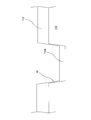
Classifications
-
- H—ELECTRICITY
- H10—SEMICONDUCTOR DEVICES; ELECTRIC SOLID-STATE DEVICES NOT OTHERWISE PROVIDED FOR
- H10W—GENERIC PACKAGES, INTERCONNECTIONS, CONNECTORS OR OTHER CONSTRUCTIONAL DETAILS OF DEVICES COVERED BY CLASS H10
- H10W20/00—Interconnections in chips, wafers or substrates
- H10W20/01—Manufacture or treatment
- H10W20/071—Manufacture or treatment of dielectric parts thereof
- H10W20/081—Manufacture or treatment of dielectric parts thereof by forming openings in the dielectric parts
- H10W20/082—Manufacture or treatment of dielectric parts thereof by forming openings in the dielectric parts the openings being tapered via holes
-
- H—ELECTRICITY
- H10—SEMICONDUCTOR DEVICES; ELECTRIC SOLID-STATE DEVICES NOT OTHERWISE PROVIDED FOR
- H10D—INORGANIC ELECTRIC SEMICONDUCTOR DEVICES
- H10D84/00—Integrated devices formed in or on semiconductor substrates that comprise only semiconducting layers, e.g. on Si wafers or on GaAs-on-Si wafers
- H10D84/01—Manufacture or treatment
- H10D84/02—Manufacture or treatment characterised by using material-based technologies
- H10D84/05—Manufacture or treatment characterised by using material-based technologies using Group III-V technology
-
- H—ELECTRICITY
- H10—SEMICONDUCTOR DEVICES; ELECTRIC SOLID-STATE DEVICES NOT OTHERWISE PROVIDED FOR
- H10W—GENERIC PACKAGES, INTERCONNECTIONS, CONNECTORS OR OTHER CONSTRUCTIONAL DETAILS OF DEVICES COVERED BY CLASS H10
- H10W20/00—Interconnections in chips, wafers or substrates
- H10W20/01—Manufacture or treatment
- H10W20/031—Manufacture or treatment of conductive parts of the interconnections
- H10W20/032—Manufacture or treatment of conductive parts of the interconnections of conductive barrier, adhesion or liner layers
- H10W20/033—Manufacture or treatment of conductive parts of the interconnections of conductive barrier, adhesion or liner layers in openings in dielectrics
- H10W20/036—Manufacture or treatment of conductive parts of the interconnections of conductive barrier, adhesion or liner layers in openings in dielectrics the barrier, adhesion or liner layers being within a main fill metal
Definitions
- the present invention relates to a power device and a method for manufacturing the power device, and more particularly to a wiring structure of a GaN-based FET.
- Compound semiconductors such as gallium nitride have higher electron mobility than silicon semiconductors, and have little change in characteristics even at high temperature operation, and have high breakdown voltage characteristics. It is attracting attention as a material for devices. In particular, utilization as a small semiconductor device capable of high withstand voltage and large current operation is desired.
- the internal wiring layer connecting the source electrode, the drain electrode, and the gate electrode ensures high reliability. And what is formed at low cost is desired.
- the current in the contact hole portion is concentrated, and in GaN using high mobility, the distance between the source and the drain is also short, and thus many contact holes must be provided. It will be costly.
- the contact hole portion 110a formed in the interlayer insulating film 110 is substantially perpendicular to the substrate plane as shown in FIG. It has a side wall W.
- metal Al or AlCu
- the film thickness of the wiring layer 112 in the side wall W portion is reduced. For this reason, the thin part of the wiring layer becomes a weak point where electromigration is likely to occur, and there is a problem that the electromigration resistance is lowered and the long-term reliability is inferior.
- an object of the present invention is to provide a power device and a power device manufacturing method capable of improving electromigration resistance and long-term reliability without using an organic material which causes film peeling.
- the power device of the present invention is: A substrate, A GaN-based semiconductor layer formed on the substrate; An electrode formed on the GaN-based semiconductor layer, or formed to be at least partially embedded in the upper portion of the GaN-based semiconductor layer; An interlayer insulating film made of silicon oxide or silicon oxynitride formed on the GaN-based semiconductor layer; A first contact hole portion formed on at least a part of the electrode and in the interlayer insulating film and having a first sidewall substantially perpendicular to the substrate plane; A second contact formed on the interlayer insulating film so as to gradually spread upward from the upper edge of the first side wall of the first contact hole portion and having a second side wall inclined with respect to the substrate plane.
- the hall A wiring layer formed in the first contact hole portion and in the second contact hole portion and on the interlayer insulating film; The wiring layer has a thickness greater than a dimension of the first side wall in the substrate thickness direction in the first contact hole portion.
- the GaN-based semiconductor layer is a semiconductor layer made of a mixed crystal material based on GaN (gallium nitride), and includes a compound such as GaN, AlGaN, InGaN, or AlInGaN.
- the wiring layer having a thickness larger than the dimension of the first sidewall in the substrate thickness direction is formed at least in the first contact hole portion in the first and second contact hole portions and on the interlayer insulating film.
- a thick interlayer insulating film can be formed and a wiring layer with a uniform thickness can be formed.
- electromigration that tends to occur in the thin wiring layer portion can be effectively suppressed. Therefore, it is possible to improve electromigration resistance and long-term reliability without using an organic material that causes film peeling for the interlayer insulating film.
- an FET using a GaN-based semiconductor capable of operating at a high voltage, a large current, and a high temperature as a power device has a high current density in a wiring layer connected to a source electrode and a drain electrode and operates at a high temperature. Although migration tends to occur, the effect of the present invention is extremely effective.
- the wiring layer is a wiring layer having a multilayer structure in which a first barrier layer, a first wiring layer, a second barrier layer, a second wiring layer, and a third barrier layer are sequentially stacked from the first barrier layer,
- the first wiring layer is thicker than the dimension of the first sidewall in the substrate thickness direction at least in the first contact hole portion.
- the first barrier layer, the first wiring layer, the second barrier layer, the second wiring layer, and the third barrier layer are laminated in order from the first barrier layer.
- the wiring layer is drawn out from the first contact hole portion through the second contact hole portion onto the interlayer insulating film without a steep step.
- the first to third barrier layers allow diffusion of the wiring layer material in the upward or downward direction in the first wiring layer and the second wiring layer without disturbing the multilayer structure of the barrier layer and causing the barrier layer to be interrupted or thinned. It can be reliably suppressed, and electromigration resistance and long-term reliability can be further improved.
- the dimension of the first side wall of the first contact hole portion in the substrate thickness direction is smaller than the dimension of the second side wall of the second contact hole portion in the substrate thickness direction.
- the dimension of the first sidewall of the first contact hole portion in the substrate thickness direction smaller than the dimension of the second sidewall of the second contact hole portion in the substrate thickness direction, It can be ensured that a thin portion is not formed in the wiring layer on the first side wall of the first contact hole portion substantially perpendicular to the substrate plane.
- the electrodes are formed on the GaN-based semiconductor layer so as to be spaced from each other, or are formed so as to be at least partially embedded in the upper portion of the GaN-based semiconductor layer.
- the wiring layer connected to the source electrode through the first and second contact hole portions extends above the gate electrode and on the interlayer insulating film from the source electrode side toward the gate electrode side. The portion formed to serve as the field plate portion.
- the gate electrode in the wiring layer connected to the source electrode through the first and second contact hole portions, extends from the source electrode side to the drain electrode side above the gate electrode and on the interlayer insulating film.
- the portion formed in this manner also serves as the field plate portion, thereby improving the breakdown voltage by relaxing the electric field strength in the GaN-based semiconductor layer while improving the resistance to electromigration and long-term reliability.
- the dimension of the inclined surface of the second side wall of the second contact hole portion at a cut surface by a plane that passes through substantially the center of the second contact hole portion and is perpendicular to the substrate plane is long.
- the inclination angle of the second side wall with respect to the substrate plane is preferably 45 degrees or less, more preferably 30 degrees or less, whereby the wiring layer can have a more uniform thickness.
- Forming a GaN-based semiconductor layer on a substrate Forming an electrode on the GaN-based semiconductor layer, or forming an electrode so as to be at least partially embedded in the upper portion of the GaN-based semiconductor layer; Forming an interlayer insulating film made of silicon oxide or silicon oxynitride on the GaN-based semiconductor layer on which the electrode is formed; Forming a second contact hole portion having a second sidewall inclined with respect to the substrate plane by wet etching so as to gradually spread upward in the interlayer insulating film; A first contact hole portion having a first side wall substantially perpendicular to the substrate plane so that at least a partial region of the electrode is exposed at a bottom portion of the second contact hole portion of the interlayer insulating film; Forming by dry etching; A wiring layer having a thickness greater than the dimension of the first sidewall in the substrate thickness direction at least in the first contact hole portion in the first contact hole portion, the second contact hole portion, and the interlayer
- the wiring layer having a thickness larger than the dimension of the first sidewall in the substrate thickness direction is formed at least in the first contact hole portion in the first and second contact hole portions and on the interlayer insulating film.
- a thin portion is not formed in the wiring layer on the first sidewall of the first contact hole portion and the second sidewall of the second contact hole portion. Migration can be effectively suppressed. Therefore, it is possible to improve electromigration resistance and long-term reliability without using an organic material that causes film peeling for the interlayer insulating film.
- the sizes of the first and second contact hole portions can be made uniform, variation in characteristics between elements in the same wafer can be suppressed.
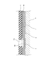
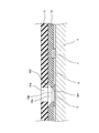
- FIG. 1 is a cross-sectional view of a power device before forming a wiring layer according to a first embodiment of the present invention.
- FIG. 2 is a cross-sectional view for explaining the manufacturing process of the power device.
- FIG. 3 is a cross-sectional view for explaining a manufacturing process subsequent to FIG.
- FIG. 4 is a cross-sectional view for explaining a manufacturing process subsequent to FIG.
- FIG. 5 is a cross-sectional view for explaining the manufacturing process subsequent to FIG.
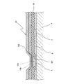
- FIG. 6 is a cross-sectional view of a power device according to the second embodiment of the present invention.
- FIG. 7 is a plan view of the main part of the power device.
- FIG. 8 is a cross-sectional view of the wiring layer of the power device.
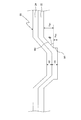
- FIG. 9 is a schematic diagram of an enlarged cross section of the main part of the power device.
- FIG. 10 is a cross-sectional view of a main part of a conventional power device.
- FIG. 1 is a sectional view of a power device according to the first embodiment of the present invention.
- the power device of the first embodiment is a GaN-based HFET (Hetero-junction Field Effect Transistor).
- the power device includes a superlattice buffer layer 2 (AlGaN / GaN), a channel layer 3 (GaN), and an example of a GaN-based semiconductor layer on an Si substrate 1.
- the barrier layer 4 (AlGaN) is formed in this order.
- a source electrode 5 and a drain electrode 6 are formed on the barrier layer 4 at an interval.
- a gate electrode 7 is formed on the barrier layer 4 in a region between the source electrode 5 and the drain electrode 6.
- the source electrode 5 and the drain electrode 6 are an alloy made of Hf / Al, and the gate electrode 7 is made of WN.
- a sapphire substrate may be used instead of the Si substrate 1, or a GaN substrate may be used.
- a superlattice buffer layer 2 two layers having different Al compositions in an AlGaN multilayer structure may be stacked, or a low temperature buffer layer may be used.
- 2DEG two-dimensional electron gas
- the gate electrode 7 is formed by selecting a material for forming a Schottky barrier with respect to the barrier layer 4. Ni / Au or TiN can also be used as the gate electrode material.
- an insulating film made of silicon nitride (SiN) is formed as the surface protective film 8 on the barrier layer 4 on which the gate electrode 7 is formed.
- the surface protective film 8 also functions as a film for suppressing collapse.
- the surface protective film does not have to be a single layer, and may be a multilayer film. In the case of a multilayer film, a silicon oxide (SiO 2 ) film may be used as an upper layer.
- the source electrode 5 and the drain electrode 6 are formed in the opening.
- the source electrode 6 and the drain electrode 7 only need to form an ohmic junction with 2DEG (two-dimensional electron gas), for example, a recess structure from which the barrier layer is removed, or an n-type barrier by doping the barrier layer.
- An ohmic electrode may be formed in the layer.
- the wiring layer is electrically connected to the source electrode 5.
- the drain electrode 7 (not shown) is also electrically connected to another wiring layer.
- silicon oxide SiO 2
- a film having a thickness of 1000 nm is formed on the barrier layer 4 (AlGaN) on which the source electrode 5, the drain electrode 6, the gate electrode 7, and the surface protective film 8 shown in FIG. 2 are formed.
- a photoresist 11 is deposited, the photoresist 11 is exposed and developed, and an opening 11a is formed in a region of the photoresist 11 where the source electrode 5 (ohmic electrode) is to be formed. To do.
- an opening having a depth of 600 nm is formed as a second contact hole portion 10b in the interlayer insulating film 10 by wet etching (isotropic etching) using buffer hydrofluoric acid.
- An opening to be the second contact hole portion 10 b of the interlayer insulating film 10 is formed so as to partially enter the lower portion of the photoresist 11.
- an opening having a depth of 400 nm is formed as a first contact hole 10a in the interlayer insulating film 10 by dry etching (anisotropic etching) using the photoresist 11 as a mask.
- the source electrode 5 (ohmic electrode) is exposed.
- the first contact hole portion having the first side wall W1 substantially perpendicular to the substrate plane by utilizing the characteristics of isotropic etching and anisotropic etching. 10a and a second contact hole portion 10b having a second side wall W2 inclined with respect to the substrate plane.
- the first side wall W1 of the first contact hole portion 10a is formed with an inclination of 90 to 80 degrees with respect to the substrate plane
- the second side wall W2 of the second contact hole portion 10b is on the substrate plane.
- 1500 nm of TiN / Al / TiN is deposited on the Si substrate 1 (shown in FIG. 1) by sputtering.
- the wiring layer 12 is formed by etching leaving the wiring region (including the contact region).
- a wiring structure having a uniform thickness including the interlayer insulating film 10 made of thick silicon oxide (SiO 2 ) can be formed.
- silicon oxide SiO 2
- silicon oxynitride containing N may be used, and B or P may be contained if the amount is small.
- AlCu may be used as the wiring layer.
- Si in the first side wall W1 is formed in the first and second contact hole portions 10a and 10b and on the interlayer insulating film 10 at least in the first contact hole portion 10a.
- the wiring layer 12 having a film thickness larger than the dimension in the thickness direction of the substrate 1
- the interlayer insulating film 10 having a large film thickness can be formed, and the wiring layer 12 having a uniform thickness can be formed.
- a thin portion is not formed in the wiring layer 12, so that an electro which is likely to occur in the thin wiring layer portion is formed. Migration can be effectively suppressed. Therefore, it is possible to improve electromigration resistance and long-term reliability without using an organic material that causes film peeling for the interlayer insulating film.
- the method for manufacturing a power device it is possible to make the sizes of the first and second contact hole portions 10a and 10b uniform, and to suppress the characteristic variation between elements in the same wafer.
- the design value of the current density of the wiring layer 12 is 1.39 ⁇ 10 5 [A / cm 2 ], which is a design condition suitable for large current operation.
- the current density of the wiring layer connected to the source electrode and the drain electrode is high, and thus, even under conditions where electromigration tends to occur, a high effect of improving electromigration resistance and long-term reliability can be obtained.
- the dimension in the substrate thickness direction of the first side wall W1 of the first contact hole portion 10a smaller than the dimension in the substrate thickness direction of the second side wall W2 of the second contact hole portion 10b, It is possible to reliably prevent the thin portion of the wiring layer 12 from being formed on the first side wall W1 of the first contact hole portion 10a substantially perpendicular to the substrate plane.
- the wiring layer 12 can be smoothly drawn out on the interlayer insulating film 10 through 10b without a step, and it is possible to surely prevent the thin portion where the electromigration easily occurs from being formed in the wiring layer 12.
- the interlayer insulating film is formed above the gate electrode 7 and from the source electrode 5 side to the drain electrode 6 side. 10 so that the portion formed so as to extend also serves as a field plate portion can improve the electromigration resistance and the long-term reliability, and reduce the electric field strength in the channel layer 3 and the barrier layer 4. Thus, the breakdown voltage can be improved.
- FIG. 6 shows a cross-sectional view of a power device according to the second embodiment of the present invention.
- the power device according to the second embodiment has the same configuration as that of the power device according to the first embodiment except for the wiring layer.
- the power device of the second embodiment is the same as the power device of the first embodiment until the step of forming the first and second contact hole portions 10a and 10b in FIG.
- the wiring layer 20 having a two-layer structure is formed by etching using a photo process while leaving the wiring region (including the contact region).
- FIG. 7 shows a plan view of the main part of the power device, which is a rectangular shape formed on at least a part of the source electrode 5 (shown in FIG. 1) or the drain electrode 6 (shown in FIG. 1).
- First and second contact hole portions 10a and 10b having a trench structure are formed, and a wiring layer 20 is formed in the first and second contact hole portions 10a and 10b and on the interlayer insulating film 10 (shown in FIG. 1). ing.
- the wiring layer 20 includes a barrier metal layer 21 (TiN with a thickness of 100 nm) as an example of a first barrier layer, a first wiring layer 22 (AlCu with a thickness of 600 nm), a second Barrier metal layer 23 (100 nm thick TiN) as an example of the barrier layer, first wiring layer 24 (600 nm thick AlCu), and barrier metal layer 25 (100 nm thick as the third barrier layer) TiN) is stacked in order from the bottom.
- a barrier metal layer 21 TiN with a thickness of 100 nm
- first wiring layer 22 AlCu with a thickness of 600 nm
- a second Barrier metal layer 23 100 nm thick TiN
- first wiring layer 24 600 nm thick AlCu
- barrier metal layer 25 100 nm thick as the third barrier layer TiN
- the power device of the second embodiment has the same effect as the power device of the first embodiment.
- the barrier metal layer 21, the first wiring layer 22, the barrier metal layer 23, the second wiring layer 24, and the barrier metal layer 25 are laminated in order from the barrier metal layer 21.
- wiring is performed from the first contact hole portion 10a to the interlayer insulating film 10 via the second contact hole portion 10b without a steep step. Since the layer 20 is pulled out, the multilayer structure of the wiring layer 20 is not disturbed, and the barrier metal layers 21, 23, 25 are not interrupted or thinned.
- the diffusion of the wiring layer material (mainly Al in the second embodiment) in the upward direction or the downward direction is ensured by the barrier metal layers 21, 23, 25. It can be suppressed and the resistance to electromigration and long-term reliability can be further improved.
- FIG. 9 is a schematic diagram of an enlarged cross section of the main part of the power device.
- H1 is the thickness of the first wiring layer 22 in the wiring layer 20 having a two-layer structure
- H2 is a two-layer structure.
- the thickness of the second wiring layer 24 H W1 is the dimension of the first side wall W1 of the first contact hole portion 10a in the substrate thickness direction
- H W2 is the second thickness of the second contact hole portion 10b.
- the dimension of the second side wall W2 in the substrate thickness direction, ⁇ is the inclination angle of the second side wall W2 of the second contact hole portion 10b with respect to the substrate plane.
- the barrier metal layers 21, 23, and 25 are omitted.
- the thickness H1 of the first wiring layer 22 the relationship between the first substrate thickness dimension H W1 of the side wall W1 of the first contact hole section 10a, H1> H W1 The conditions are satisfied.
- the service life can be drastically improved.
- Table 1 shows the result of calculating the lifetimes of the one-layer wiring layer of the first embodiment and the two-layer wiring layer of the second embodiment by performing an acceleration test.
- the environmental temperature is set to 250 ° C., and a constant current of 1.33 ⁇ 10 6 [A / cm 2 ] is passed from the constant current source to the wiring layer to be tested, and the change with time of the voltage across the wiring layer is measured. Measure the change of the resistance of the wiring layer over time based on the constant current flowing in the wiring layer and the voltage across the wiring layer, and determine that each of the wiring layers is defective when the resistance of the wiring layer fluctuates 10% from the initial value. The life of the wiring layer was determined.
- A is the shape factor
- J is the current density
- Ea is the activation energy (specific to the Al wiring)
- k is the Boltzmann constant
- T is the absolute temperature.
- the absolute temperature T is an absolute temperature estimated when a temperature characteristic is measured in advance and a current is passed at 1.33 ⁇ 10 6 [A / cm 2 ].
- J is 1.4 ⁇ 10 5 [A / cm 2 ].
- uniform wiring can be obtained by setting the first wiring layer 22 (AlCu) of the first layer to a thickness of 600 nm and thicker than the height of the first side wall W1. As a result, the electromigration characteristics could be sufficiently improved.
- the contact hole has two steps, and the thickness of the first wiring layer 22 is the depth of the first contact hole portion in the first step.
- the GaN HFET in which the source electrode 5, the drain electrode 6, and the gate electrode 7 are formed on the barrier layer 4 as the power device has been described.
- at least one GaN HFET is formed on the GaN semiconductor layer.
- the present invention may be applied to a power device having a source electrode and a drain electrode formed so as to be spaced from each other so that the portion is embedded.
- the power device when the source electrode and the drain electrode are all formed on the GaN-based semiconductor layer with a space between them, and when the GaN-based semiconductor layer is etched, the power device is spaced 2 from each other.
- the source electrode and the drain electrode are formed so that a part of the lower side of the source electrode and the drain electrode is embedded in each recess.
- one of the source electrode and the drain electrode may be entirely formed on the GaN-based semiconductor layer, and the other of the source electrode or the drain electrode may be at least partially formed in the GaN-based semiconductor layer.
- the GaN-based semiconductor layer of the power device according to the present invention only needs to be expressed by Al x In y Ga 1-xy N (x ⁇ 0, y ⁇ 0, 0 ⁇ x + y ⁇ 1). That is, the GaN-based semiconductor layer is not limited to GaN, but may be AlGaN, InGaN, or AlInGaN.
- the power device of the present invention is not limited to the HFET of the first and second embodiments, but may be a field effect transistor having another configuration.
Landscapes
- Electrodes Of Semiconductors (AREA)
- Internal Circuitry In Semiconductor Integrated Circuit Devices (AREA)
- Junction Field-Effect Transistors (AREA)
Abstract
バリア層(4)(AlGaN)上に形成された酸化シリコン(SiO2)からなる層間絶縁膜(10)と、層間絶縁膜(10)のソース電極(5)上に形成され、基板平面に対して略垂直な第1の側壁(W1)を有する第1コンタクトホール部(11a)と、第1コンタクトホール部(11a)の第1の側壁(W1)の上縁から上側に向かって徐々に広がるように層間絶縁膜(10)に形成され、基板平面に対して傾斜した第2の側壁(W2)を有する第2コンタクトホール部(11b)と、第1,第2コンタクトホール部(11a,11b)内および層間絶縁膜(10)上に形成された配線層(12)とを備える。上記配線層(12)は、第1コンタクトホール部(11a)において第1の側壁(W1)の基板厚さ方向の寸法よりも膜厚が厚い。これにより、膜剥がれの要因となる有機材料を用いることなく、エレクトロマイグレーションの耐性と長期信頼性を向上できるパワーデバイスを提供する。
Description
この発明は、パワーデバイスおよびパワーデバイスの製造方法に関し、特にGaN系FETの配線構造に関する。
窒化ガリウムなどの化合物半導体は、シリコン半導体に比べて、電子移動度が高く、また、高温動作においても特性の変化が少なく、高耐圧の特性を有しているので、スイッチング装置などに用いられるパワーデバイスの材料として注目されている。特に、高耐圧、大電流動作が可能な小型半導体素子としての活用が望まれている。
このような小型で、大電流動作が可能なGaN系FET(Field Effect Transistor:電界効果トランジスタ)において、ソース電極とドレイン電極およびゲート電極を接続する内部配線層では、高い信頼性を確保して、かつ、低コストで形成されるものが望まれている。
従来、パワーデバイスとしては、層間絶縁膜をポリイミドで形成し、コンタクト領域にコンタクトホールを形成して、そのコンタクトホール内にAuなどのプラグを形成したものがある(例えば、特開2003-142501号公報(特許文献1)参照)。
上記従来のパワーデバイスでは、コンタクトホール部での電流が集中する上に、高移動度を用いたGaNにおいては、ソース・ドレイン間の距離も短いことから多くのコンタクトホールを設けざるを得ず、コストが掛かることになる。
また、ポリイミドなどの有機絶縁膜を層間絶縁膜として用いる場合には、有機材料であるために変質が避けられず、長期信頼性が得られないという問題がある。
また、本発明者らが鋭意検討したところ、有機材料と絶縁膜との密着性や有機材料と金属配線との密着性が悪く、膜剥がれの問題を引き起こすことがあることが明らかになった。このような有機材料と絶縁膜との密着性や有機材料と金属配線との密着性を上げるために、通常用いられる逆スパッタにより密着面の表面積を増加させる方法は、有機材料が変質してしまうので使用することができない。
また、上記従来のパワーデバイスにおいてSiO2膜を層間絶縁膜として用いる場合には、図10に示すように、層間絶縁膜110に形成されたコンタクトホール部110aは、基板平面に対して略垂直な側壁Wを有する。このようなコンタクトホール部110a内および層間絶縁膜110上にスパッタリングにより金属(AlまたはAlCuなど)を堆積して配線層112を形成するとき、コンタクトホール部110aの側壁Wに金属が堆積しにくいため、側壁W部分の配線層112の膜厚が薄くなる。このため、配線層の膜厚の薄い部分は、エレクトロマイグレーションが生じやすいウィークポイントとなり、エレクトロマイグレーションの耐性が低下して長期信頼性が劣るという問題がある。
そこで、この発明の課題は、膜剥がれの要因となる有機材料を用いることなく、エレクトロマイグレーションの耐性と長期信頼性を向上できるパワーデバイスおよびパワーデバイスの製造方法を提供することにある。
上記課題を解決するため、この発明のパワーデバイスは、
基板と、
上記基板上に形成されたGaN系半導体層と、
上記GaN系半導体層上に形成されているか、または、上記GaN系半導体層の上部に少なくとも一部が埋め込まれるように形成された電極と、
上記GaN系半導体層上に形成された酸化シリコンまたは酸窒化シリコンからなる層間絶縁膜と、
上記電極の少なくとも一部の領域上かつ上記層間絶縁膜に形成され、上記基板平面に対して略垂直な第1の側壁を有する第1コンタクトホール部と、
上記第1コンタクトホール部の上記第1の側壁の上縁から上側に向かって徐々に広がるように上記層間絶縁膜に形成され、上記基板平面に対して傾斜した第2の側壁を有する第2コンタクトホール部と、
上記第1コンタクトホール部内と上記第2コンタクトホール部内および上記層間絶縁膜上に形成された配線層と
を備え、
上記配線層は、上記第1コンタクトホール部において上記第1の側壁の上記基板厚さ方向の寸法よりも膜厚が厚いことを特徴とする。
基板と、
上記基板上に形成されたGaN系半導体層と、
上記GaN系半導体層上に形成されているか、または、上記GaN系半導体層の上部に少なくとも一部が埋め込まれるように形成された電極と、
上記GaN系半導体層上に形成された酸化シリコンまたは酸窒化シリコンからなる層間絶縁膜と、
上記電極の少なくとも一部の領域上かつ上記層間絶縁膜に形成され、上記基板平面に対して略垂直な第1の側壁を有する第1コンタクトホール部と、
上記第1コンタクトホール部の上記第1の側壁の上縁から上側に向かって徐々に広がるように上記層間絶縁膜に形成され、上記基板平面に対して傾斜した第2の側壁を有する第2コンタクトホール部と、
上記第1コンタクトホール部内と上記第2コンタクトホール部内および上記層間絶縁膜上に形成された配線層と
を備え、
上記配線層は、上記第1コンタクトホール部において上記第1の側壁の上記基板厚さ方向の寸法よりも膜厚が厚いことを特徴とする。
ここで、GaN系半導体層とは、GaN(窒化ガリウム)をベースとした混晶材料からなる半導体層であり、GaN、AlGaN、InGaN、AlInGaN等の化合物を含むものである。
上記構成によれば、第1,第2コンタクトホール部内および層間絶縁膜上に、少なくとも第1コンタクトホール部において第1の側壁の基板厚さ方向の寸法よりも膜厚が厚い配線層を形成することによって、膜厚の厚い層間絶縁膜にできると共に、均一な厚さの配線層にすることができ、第1コンタクトホール部の第1の側壁および第2コンタクトホール部の第2の側壁において、配線層に膜厚の薄い部分が形成されないので、膜厚の薄い配線層部分に生じやすいエレクトロマイグレーションを効果的に抑制できる。したがって、膜剥がれの要因となる有機材料を層間絶縁膜に用いることなく、エレクトロマイグレーションの耐性と長期信頼性を向上できる。
特に、パワーデバイスとして、高耐圧で大電流,高温動作が可能なGaN系半導体を用いたFETでは、ソース電極やドレイン電極に接続される配線層の電流密度が高くかつ高温動作となるので、エレクトロマイグレーションが発生しやすくなるが、この発明の効果が極めて有効である。
また、一実施形態のパワーデバイスでは、
上記配線層は、第1バリア層と第1配線層と第2バリア層と第2配線層および第3バリア層が上記第1バリア層から順に積層された多層構造の配線層であり、
上記第1配線層は、少なくとも上記第1コンタクトホール部において上記第1の側壁の上記基板厚さ方向の寸法よりも膜厚が厚い。
上記配線層は、第1バリア層と第1配線層と第2バリア層と第2配線層および第3バリア層が上記第1バリア層から順に積層された多層構造の配線層であり、
上記第1配線層は、少なくとも上記第1コンタクトホール部において上記第1の側壁の上記基板厚さ方向の寸法よりも膜厚が厚い。
上記実施形態によれば、第1バリア層と第1配線層と第2バリア層と第2配線層および第3バリア層が第1バリア層から順に積層された多層構造の配線層を、第1,第2コンタクトホール部内および層間絶縁膜上に形成することによって、第1コンタクトホール部内から第2コンタクトホール部を介して層間絶縁膜上に急な段差なしに配線層が引き出されるので、配線層の多層構造が乱れてバリア層が途切れたり薄くなったりすることがなく、第1配線層および第2配線層において上方向または下方向への配線層材料の拡散を第1~第3バリア層により確実に抑制でき、エレクトロマイグレーションの耐性と長期信頼性をさらに向上できる。
また、一実施形態のパワーデバイスでは、
上記第1コンタクトホール部の上記第1の側壁の上記基板厚さ方向の寸法は、上記第2コンタクトホール部の上記第2の側壁の上記基板厚さ方向の寸法よりも小さい。
上記第1コンタクトホール部の上記第1の側壁の上記基板厚さ方向の寸法は、上記第2コンタクトホール部の上記第2の側壁の上記基板厚さ方向の寸法よりも小さい。
上記実施形態によれば、第1コンタクトホール部の第1の側壁の基板厚さ方向の寸法を、第2コンタクトホール部の第2の側壁の基板厚さ方向の寸法よりも小さくすることによって、基板平面に対して略垂直な第1コンタクトホール部の第1の側壁において配線層に膜厚の薄い部分が形成されないように確実にできる。
また、一実施形態のパワーデバイスでは、
上記電極は、上記GaN系半導体層上に互いに間隔をあけて形成されているか、または、上記GaN系半導体層の上部に少なくとも一部が埋め込まれるように互いに間隔をあけて形成されたソース電極およびドレイン電極と、上記GaN系半導体層上かつ上記ソース電極と上記ドレイン電極との間に形成されたゲート電極を含み、
上記ソース電極に上記第1,第2コンタクトホール部を介して接続された上記配線層は、上記ソース電極側から上記ゲート電極側に向かって上記ゲート電極の上方かつ上記層間絶縁膜上に延在するように形成された部分がフィールドプレート部を兼ねる。
上記電極は、上記GaN系半導体層上に互いに間隔をあけて形成されているか、または、上記GaN系半導体層の上部に少なくとも一部が埋め込まれるように互いに間隔をあけて形成されたソース電極およびドレイン電極と、上記GaN系半導体層上かつ上記ソース電極と上記ドレイン電極との間に形成されたゲート電極を含み、
上記ソース電極に上記第1,第2コンタクトホール部を介して接続された上記配線層は、上記ソース電極側から上記ゲート電極側に向かって上記ゲート電極の上方かつ上記層間絶縁膜上に延在するように形成された部分がフィールドプレート部を兼ねる。
上記実施形態によれば、ソース電極に第1,第2コンタクトホール部を介して接続された配線層において、ソース電極側からドレイン電極側に向かってゲート電極の上方かつ層間絶縁膜上に延在するように形成された部分がフィールドプレート部を兼ねることによって、エレクトロマイグレーションの耐性と長期信頼性を向上しつつ、GaN系半導体層における電界強度を緩和することで耐圧を向上できる。
また、一実施形態のパワーデバイスでは、
上記第2コンタクトホール部の略中央を通りかつ上記基板平面に対して垂直な平面による切断面において、上記第2コンタクトホール部の上記第2の側壁の傾斜面の上記基板厚さ方向の寸法よりも上記第2の側壁の傾斜面の上記基板平面に沿った方向の寸法が長い。
上記第2コンタクトホール部の略中央を通りかつ上記基板平面に対して垂直な平面による切断面において、上記第2コンタクトホール部の上記第2の側壁の傾斜面の上記基板厚さ方向の寸法よりも上記第2の側壁の傾斜面の上記基板平面に沿った方向の寸法が長い。
上記実施形態によれば、第2コンタクトホール部の略中央を通りかつ基板平面に対して垂直な平面による切断面において、第2コンタクトホール部の第2の側壁の傾斜面の基板厚さ方向の寸法よりも第2の側壁の傾斜面の基板平面に沿った方向の寸法を長くすることによって、第2の側壁がゆるやかに傾斜するので、第1コンタクトホール部内から第2コンタクトホール部を介して層間絶縁膜上に段差なくスムーズに配線層を引き出すことができ、エレクトロマイグレーションが生じやすい膜厚の薄い部分が配線層に形成されるのを確実に防ぐことができる。
例えば、基板平面に対して第2の側壁の傾斜角度は45度以下が好ましく、より好ましくは30度以下であり、これにより、配線層をより均一な厚さにすることができる。
また、この発明のパワーデバイスの製造方法では、
基板上にGaN系半導体層を形成する工程と、
上記GaN系半導体層上に電極を形成するか、または、上記GaN系半導体層の上部に少なくとも一部が埋め込まれるように電極を形成する工程と、
上記電極が形成された上記GaN系半導体層上に酸化シリコンまたは酸窒化シリコンからなる層間絶縁膜を形成する工程と、
上記層間絶縁膜に上側に向かって徐々に広がるように、上記基板平面に対して傾斜した第2の側壁を有する第2コンタクトホール部をウェットエッチングにより形成する工程と、
上記層間絶縁膜の上記第2コンタクトホール部の底部に、上記電極の少なくとも一部の領域が露出するように、上記基板平面に対して略垂直な第1の側壁を有する第1コンタクトホール部をドライエッチングにより形成する工程と、
上記第1コンタクトホール部内と上記第2コンタクトホール部内および上記層間絶縁膜上に、少なくとも上記第1コンタクトホール部において上記第1の側壁の上記基板厚さ方向の寸法よりも膜厚が厚い配線層を形成する工程と
を含むことを特徴とする。
基板上にGaN系半導体層を形成する工程と、
上記GaN系半導体層上に電極を形成するか、または、上記GaN系半導体層の上部に少なくとも一部が埋め込まれるように電極を形成する工程と、
上記電極が形成された上記GaN系半導体層上に酸化シリコンまたは酸窒化シリコンからなる層間絶縁膜を形成する工程と、
上記層間絶縁膜に上側に向かって徐々に広がるように、上記基板平面に対して傾斜した第2の側壁を有する第2コンタクトホール部をウェットエッチングにより形成する工程と、
上記層間絶縁膜の上記第2コンタクトホール部の底部に、上記電極の少なくとも一部の領域が露出するように、上記基板平面に対して略垂直な第1の側壁を有する第1コンタクトホール部をドライエッチングにより形成する工程と、
上記第1コンタクトホール部内と上記第2コンタクトホール部内および上記層間絶縁膜上に、少なくとも上記第1コンタクトホール部において上記第1の側壁の上記基板厚さ方向の寸法よりも膜厚が厚い配線層を形成する工程と
を含むことを特徴とする。
上記構成によれば、第1,第2コンタクトホール部内および層間絶縁膜上に、少なくとも第1コンタクトホール部において第1の側壁の基板厚さ方向の寸法よりも膜厚が厚い配線層を形成することによって、第1コンタクトホール部の第1の側壁および第2コンタクトホール部の第2の側壁において、配線層に膜厚の薄い部分が形成されないので、膜厚の薄い配線層部分に生じやすいエレクトロマイグレーションを効果的に抑制できる。したがって、膜剥がれの要因となる有機材料を層間絶縁膜に用いることなく、エレクトロマイグレーションの耐性と長期信頼性を向上できる。また、第1,第2コンタクトホール部の大きさを均一にすることができるので、同一ウェハ内の素子間の特性バラツキを抑えることができる。
以上より明らかなように、この発明のパワーデバイスおよびパワーデバイスの製造方法によれば、膜剥がれの要因となる有機材料を用いることなく、エレクトロマイグレーションの耐性と長期信頼性を向上できる大電流動作,高温動作に適したパワーデバイスを実現することができる。
以下、この発明のパワーデバイスおよびパワーデバイスの製造方法を図示の実施の形態により詳細に説明する。
〔第1実施形態〕
図1はこの発明の第1実施形態のパワーデバイスの断面図を示している。この第1実施形態のパワーデバイスは、GaN系HFET(Hetero-junction Field Effect Transistor;ヘテロ接合電界効果トランジスタ)である。
図1はこの発明の第1実施形態のパワーデバイスの断面図を示している。この第1実施形態のパワーデバイスは、GaN系HFET(Hetero-junction Field Effect Transistor;ヘテロ接合電界効果トランジスタ)である。
この第1実施形態のパワーデバイスは、図1に示すように、Si基板1上に、GaN系半導体層の一例として、超格子バッファ層2(AlGaN/GaN)と、チャネル層3(GaN)と、バリア層4(AlGaN)とを順に形成している。上記バリア層4上に間隔をあけてソース電極5とドレイン電極6を形成している。このソース電極5とドレイン電極6との間の領域かつバリア層4上にゲート電極7を形成している。ソース電極5とドレイン電極6はHf/Alからなる合金であり、ゲート電極7はWNからなる。
なお、Si基板1の代わりにサファイア基板でもよいし、GaN基板を用いてもよい。また、超格子バッファ層2として、AlGaN多層構造でAl組成を異ならせた2層を積層してもよく、低温バッファ層でも構わない。
上記パワーデバイスにおいて、チャネル層3とバリア層4のバンドギャップ差により、GaNからなるチャネル層3側の表面近傍に2DEG(2次元電子ガス)が形成される。
ゲート電極7は、バリア層4に対してショットキー障壁が形成される材料を選択して形成する。ゲート電極材料として、Ni/AuやTiNなども用いることができる。
なお、ソース電極5とドレイン電極6を形成する前に、ゲート電極7が形成されたバリア層4上に表面保護膜8として窒化シリコン(SiN)からなる絶縁膜を形成している。この表面保護膜8は、コラプスを抑制するための膜としても機能する。また、表面保護膜は、単層である必要はなく、多層膜であってもよく、多層膜の場合には、酸化シリコン(SiO2)膜を上層にしてもよい。
そして、表面保護膜8のソース電極とドレイン電極が形成されるべき領域に開口を設けた後、その開口内にソース電極5とドレイン電極6を形成する。
このソース電極6およびドレイン電極7は、2DEG(2次元電子ガス)とのオーミック接合が形成されればよいので、例えば、バリア層を除去したリセス構造や、バリア層にドープを行なってn型バリア層としたところにオーミック電極を形成しても構わない。
次に、図2~図5に従って配線層を形成する工程について説明する。なお、図2~図5では、ソース電極5に配線層が電気的に接続されているが、図示しないドレイン電極7も同様にして他の配線層が電気的に接続されている。
まず、図2に示すソース電極5とドレイン電極6とゲート電極7および表面保護膜8が形成されたバリア層4(AlGaN)上に、プラズマCVDを用いて層間絶縁膜10として酸化シリコン(SiO2)膜を厚さ1000nm形成する。
次に、図3に示すように、フォトレジスト11を堆積し、フォトレジスト11を露光,現像して、フォトレジスト11のソース電極5(オーミック電極)が形成されるべき領域に開口部11aを形成する。
次に、バッファフッ酸を用いたウェットエッチング(等方性エッチング)により層間絶縁膜10に600nmの深さの開口部を第2コンタクトホール部10bとして形成する。この層間絶縁膜10の第2コンタクトホール部10bとなる開口部は、フォトレジスト11の下部に一部入り込む形で形成される。
次に、図4に示すように、ドライエッチング(異方性エッチング)により、フォトレジスト11をマスクにして層間絶縁膜10に400nmの深さの開口部を第1コンタクトホール部10aとして形成することによって、ソース電極5(オーミック電極)を露出させる。
上記ウェットエッチングおよびドライエッチングの条件を適切に選ぶことによって、等方性エッチングと異方性エッチングの特性を生かして、基板平面に対して略垂直な第1の側壁W1を有する第1コンタクトホール部10aと、基板平面に対して傾斜した第2の側壁W2を有する第2コンタクトホール部10bを形成する。実際には、第1コンタクトホール部10aの第1の側壁W1は、基板平面に対して90~80度の傾きで形成し、第2コンタクトホール部10bの第2の側壁W2は、基板平面に対して45~20度の傾きに形成することができる。
なお、次の工程における配線層を形成するスパッタの均一性を向上させるには、第2コンタクトホール部10bの第2の側壁W2の基板平面に対する傾きを30度以下の構造にすることが好ましい。
次に、図5に示すように、スパッタ法によりSi基板1(図1に示す)上にTiN/Al/TiNを1500nm堆積させる。次に、フォト工程を用いて、配線領域(コンタクト領域を含む)を残してエッチングすることによって、配線層12を形成する。
以上の工程によって、厚い酸化シリコン(SiO2)からなる層間絶縁膜10を有した均一な厚さの配線構造を形成することができる。
なお、層間絶縁膜として、耐圧を確保する観点から酸化シリコン(SiO2)が好ましいが、Nを含んだ酸窒化シリコンでもよく、また微量であればBやPを含んでいてもよい。また、配線層としては、AlCuを用いてもよい。
上記構成のパワーデバイスおよびパワーデバイスの製造方法によれば、第1,第2コンタクトホール部10a,10b内および層間絶縁膜10上に、少なくとも第1コンタクトホール部10aにおいて第1の側壁W1のSi基板1厚さ方向の寸法よりも膜厚が厚い配線層12を形成することによって、膜厚の厚い層間絶縁膜10にできると共に、均一な厚さの配線層12にすることができ、第1コンタクトホール部10aの第1の側壁W1および第2コンタクトホール部10bの第2の側壁W2において、配線層12に膜厚の薄い部分が形成されないので、膜厚の薄い配線層部分に生じやすいエレクトロマイグレーションを効果的に抑制できる。したがって、膜剥がれの要因となる有機材料を層間絶縁膜に用いることなく、エレクトロマイグレーションの耐性と長期信頼性を向上できる。
また、上記パワーデバイスの製造方法によれば、第1,第2コンタクトホール部10a,10bの大きさを均一にすることが可能となり、同一ウェハ内の素子間の特性バラツキを抑えることができる。
上記第1実施形態のパワーデバイスでは、配線層12の電流密度の設計値は1.39×10⁵[A/cm2]とし、大電流動作に適した設計条件としている。このような大電流動作に対応し、かつ、高耐圧で高温動作が可能なGaN系半導体を用いたパワーデバイスにおいて、ソース電極やドレイン電極に接続される配線層の電流密度が高くかつ高温動作となってエレクトロマイグレーションが発生しやすい条件でも、エレクトロマイグレーションの耐性と長期信頼性が向上するという高い効果が得られる。
また、上記第1コンタクトホール部10aの第1の側壁W1の基板厚さ方向の寸法を、第2コンタクトホール部10bの第2の側壁W2の基板厚さ方向の寸法よりも小さくすることによって、基板平面に対して略垂直な第1コンタクトホール部10aの第1の側壁W1において配線層12に膜厚の薄い部分が形成されるのを確実に防止できる。
また、上記第2コンタクトホール部10bの略中央を通りかつ基板平面に対して垂直な平面による切断面において、第2コンタクトホール部10bの第2の側壁W2の傾斜面の基板厚さ方向の寸法よりも第2の側壁W2の傾斜面の基板平面に沿った方向の寸法を長くすることによって、第2の側壁W2がゆるやかに傾斜するので、第1コンタクトホール部10a内から第2コンタクトホール部10bを介して層間絶縁膜10上に段差なくスムーズに配線層12を引き出すことができ、エレクトロマイグレーションが生じやすい膜厚の薄い部分が配線層12に形成されるのを確実に防ぐことができる。
なお、上記ソース電極5に第1,第2コンタクトホール部10a,10bを介して接続された配線層12において、ソース電極5側からドレイン電極6側に向かってゲート電極7の上方かつ層間絶縁膜10上に延在するように形成された部分がフィールドプレート部を兼ねるようにすることによって、エレクトロマイグレーションの耐性と長期信頼性を向上しつつ、チャネル層3とバリア層4における電界強度を緩和することで耐圧を向上できる。
〔第2実施形態〕
図6はこの発明の第2実施形態のパワーデバイスの断面図を示している。この第2実施形態のパワーデバイスは、配線層を除いて第1実施形態のパワーデバイスと同一の構成をしており、同一構成部には同一参照番号を付して説明を省略する。
図6はこの発明の第2実施形態のパワーデバイスの断面図を示している。この第2実施形態のパワーデバイスは、配線層を除いて第1実施形態のパワーデバイスと同一の構成をしており、同一構成部には同一参照番号を付して説明を省略する。
この第2実施形態のパワーデバイスは、図4の第1,第2コンタクトホール部10a,10bを形成する工程までは、上記第1実施形態のパワーデバイスと同じである。
第1,第2コンタクトホール部10a,10bの形成工程の次に、図6に示すように、スパッタ法によりSi基板1上にTiN/AlCu/TiN/AlCu/TiNを1500nm堆積させる。
次に、フォト工程を用いて、配線領域(コンタクト領域を含む)を残してエッチングすることによって、2層構造の配線層20を形成する。
図7は上記パワーデバイスの要部の平面図を示しており、ソース電極5(図1に示す)またはドレイン電極6(図1に示す)の少なくとも一部の領域上に形成された長方形状のトレンチ構造の第1,第2コンタクトホール部10a,10bを形成し、その第1,第2コンタクトホール部10a,10b内および層間絶縁膜10(図1に示す)上に配線層20を形成している。
上記配線層20は、図8に示すように、第1バリア層の一例としてのバリアメタル層21(厚さ100nmのTiN)と、第1配線層22(厚さ600nmのAlCu)と、第2バリア層の一例としてのバリアメタル層23(厚さ100nmのTiN)と、第1配線層24(厚さ600nmのAlCu)と、第3バリア層の一例としてのバリアメタル層25(厚さ100nmのTiN)が下側から順に積層された構造をしている。
上記第2実施形態のパワーデバイスは、第1実施形態のパワーデバイスと同様の効果を有する。
また、上記バリアメタル層21と第1配線層22とバリアメタル層23と第2配線層24およびバリアメタル層25がバリアメタル層21から順に積層された多層構造の配線層20を、第1,第2コンタクトホール部10a,10b内および層間絶縁膜10上に形成することによって、第1コンタクトホール部10a内から第2コンタクトホール部10bを介して層間絶縁膜10上に急な段差なしに配線層20が引き出されるので、配線層20の多層構造が乱れてバリアメタル層21,23,25が途切れたり薄くなったりすることがない。この場合、第1配線層22および第2配線層24において上方向または下方向への配線層材料(この第2実施形態では主にAl)の拡散をバリアメタル層21,23,25により確実に抑制でき、エレクトロマイグレーションの耐性と長期信頼性をさらに向上できる。
図9は上記パワーデバイスの要部の拡大断面の模式図を示しており、図9において、H1は2層構造の配線層20のうちの第1配線層22の厚さ、H2は2層構造の配線層20のうちの第2配線層24の厚さ、HW1は第1コンタクトホール部10aの第1の側壁W1の基板厚さ方向の寸法、HW2は第2コンタクトホール部10bの第2の側壁W2の基板厚さ方向の寸法、θは第2コンタクトホール部10bの第2の側壁W2の基板平面に対する傾斜角度である。なお、図9では、バリアメタル層21,23,25を省略している。
上記第1配線層22の厚さH1と、第1コンタクトホール部10aの第1の側壁W1の基板厚さ方向の寸法HW1との関係は、
H1 > HW1
の条件を満足している。
H1 > HW1
の条件を満足している。
このような2層構造の配線層20にすることによって、寿命を飛躍的に向上させることができる。
表1は、加速度試験を行って、第1実施形態の1層構造の配線層および第2実施形態の2層構造の配線層の寿命を算出した結果を示している。

この加速度試験では、環境温度を250℃とし、試験対象となる配線層に1.33×10⁶[A/cm2]の一定電流を定電流源から流して配線層の両端電圧の経時変化を測定し、上記配線層に流れる一定電流と配線層の両端電圧に基づいて配線層の抵抗の経時変化を求めて、配線層の抵抗が初期値から10%変動したところで不良と判定することにより各配線層の寿命を求めた。
そして、上記加速度試験の結果から得られた各配線層の寿命に基づいて、配線層の材質,構造などに関係する定数である形状因子Aを次の(式1)により求める。
寿命 = AJ-2exp(Ea/kT) ……… (式1)
ここで、Aは形状因子、Jは電流密度、Eaは活性化エネルギー(Al配線固有)、kはボルツマン定数、Tは絶対温度である。また、絶対温度Tは、事前に温度特性を測定して、1.33×10⁶[A/cm2]で電流を流した時に見積もられた絶対温度である。
寿命 = AJ-2exp(Ea/kT) ……… (式1)
ここで、Aは形状因子、Jは電流密度、Eaは活性化エネルギー(Al配線固有)、kはボルツマン定数、Tは絶対温度である。また、絶対温度Tは、事前に温度特性を測定して、1.33×10⁶[A/cm2]で電流を流した時に見積もられた絶対温度である。
そうして、得られた形状因子Aを用いて、Tを423.15[k](=273.15[℃]+150[℃])、Jを1.4×10⁵[A/cm2]の条件で上記(式1)により寿命を算出すると、第1実施形態の1層構造の配線層では71年となり、第2実施形態の2層構造の配線層では261年となった。2層構造の配線層は、1層構造の配線層よりも寿命が約3.6倍延びる。
上記第2実施形態では、1層目の第1配線層22(AlCu)を厚さ600nmとして、第1の側壁W1の高さよりも厚くすることで、均一な配線とすることができる。これにより、エレクトロマイグレーション特性を十分に改善することができた。
上記第2実施形態のパワーデバイスにおいて、2層構造の配線層20とする場合には、コンタクトホールを2段階とし、第1配線層22の厚さを1段階目の第1コンタクトホール部の深さより大きくすることによって、配線層に膜厚の薄い部分が生じるのを効果的に抑制することができる。
上記第1,第2実施形態では、パワーデバイスとしてバリア層4上にソース電極5とドレイン電極6およびゲート電極7が形成されたGaN系HFETについて説明したが、GaN系半導体層の上部に少なくとも一部が埋め込まれるように互いに間隔をあけて形成されたソース電極,ドレイン電極を有するパワーデバイスにこの発明を適用してもよい。
すなわち、この発明のパワーデバイスでは、GaN系半導体層上に互いに間隔をあけてソース電極,ドレイン電極の全部が形成されている場合と、GaN系半導体層をエッチングすることにより互いに間隔をあけて2つの凹部を形成して、その各凹部内にソース電極,ドレイン電極の全部が形成されている場合と、さらに、GaN系半導体層をエッチングすることにより互いに間隔をあけて2つの凹部を形成して、その各凹部内にソース電極,ドレイン電極の下側の一部が埋め込まれるように、ソース電極,ドレイン電極が形成されている場合がある。なお、ソース電極またはドレイン電極の一方は、GaN系半導体層上に全部が形成され、ソース電極またはドレイン電極の他方は、GaN系半導体層内に少なくとも一部が形成されていてもよい。
この発明のパワーデバイスのGaN系半導体層は、AlxInyGa1-x-yN(x≧0、y≧0、0≦x+y≦1)で表されるものであればよい。すなわち、GaN系半導体層は、GaNに限らず、AlGaN、InGaN、AlInGaNでもよい。
また、この発明のパワーデバイスは、上記第1,第2実施形態のHFETに限らず、他の構成の電界効果トランジスタであってもよい。
この発明の具体的な実施の形態について説明したが、この発明は上記第1,第2実施形態に限定されるものではなく、この発明の範囲内で種々変更して実施することができる。
1…Si基板
2…超格子バッファ層
3…チャネル層
4…バリア層
5…ソース電極
6…ドレイン電極
7…ゲート電極
8…表面保護膜
10…層間絶縁膜
10a…第1コンタクトホール部
10b…第2コンタクトホール部
11…フォトレジスト
12,20…配線層
21,23,25…バリアメタル層
22…第1配線層
24…第2配線層
2…超格子バッファ層
3…チャネル層
4…バリア層
5…ソース電極
6…ドレイン電極
7…ゲート電極
8…表面保護膜
10…層間絶縁膜
10a…第1コンタクトホール部
10b…第2コンタクトホール部
11…フォトレジスト
12,20…配線層
21,23,25…バリアメタル層
22…第1配線層
24…第2配線層
Claims (6)
- 基板(1)と、
上記基板(1)上に形成されたGaN系半導体層(2,3,4)と、
上記GaN系半導体層(2,3,4)上に形成されているか、または、上記GaN系半導体層(2,3,4)の上部に少なくとも一部が埋め込まれるように形成された電極(5,6,7)と、
上記GaN系半導体層(2,3,4)上に形成された酸化シリコンまたは酸窒化シリコンからなる層間絶縁膜(10)と、
上記電極(5,6,7)の少なくとも一部の領域上かつ上記層間絶縁膜(10)に形成され、上記基板(1)平面に対して略垂直な第1の側壁を有する第1コンタクトホール部(10a)と、
上記第1コンタクトホール部(10a)の上記第1の側壁の上縁から上側に向かって徐々に広がるように上記層間絶縁膜(10)に形成され、上記基板(1)平面に対して傾斜した第2の側壁を有する第2コンタクトホール部(10b)と、
上記第1コンタクトホール部(10a)内と上記第2コンタクトホール部(10b)内および上記層間絶縁膜(10)上に形成された配線層(12,20)と
を備え、
上記配線層(12,20)は、上記第1コンタクトホール部(10a)において上記第1の側壁の上記基板(1)厚さ方向の寸法よりも膜厚が厚いことを特徴とするパワーデバイス。 - 請求項1に記載のパワーデバイスにおいて、
上記配線層(20)は、第1バリア層(21)と第1配線層(22)と第2バリア層(23)と第2配線層(24)および第3バリア層(25)が上記第1バリア層(21)から順に積層された多層構造の配線層であり、
上記第1配線層(22)は、少なくとも上記第1コンタクトホール部(10a)において上記第1の側壁の上記基板(1)厚さ方向の寸法よりも膜厚が厚いことを特徴とするパワーデバイス。 - 請求項1または2に記載のパワーデバイスにおいて、
上記第1コンタクトホール部(10a)の上記第1の側壁の上記基板(1)厚さ方向の寸法は、上記第2コンタクトホール部(10b)の上記第2の側壁の上記基板(1)厚さ方向の寸法よりも小さいことを特徴とするパワーデバイス。 - 請求項1から3までのいずれか1つに記載のパワーデバイスにおいて、
上記電極(5,6,7)は、上記GaN系半導体層(2,3,4)上に互いに間隔をあけて形成されているか、または、上記GaN系半導体層(2,3,4)の上部に少なくとも一部が埋め込まれるように互いに間隔をあけて形成されたソース電極(5)およびドレイン電極(6)と、上記GaN系半導体層(2,3,4)上かつ上記ソース電極(5)と上記ドレイン電極(6)との間に形成されたゲート電極(7)を含み、
上記ソース電極(5)に上記第1,第2コンタクトホール部(10a,10b)を介して接続された上記配線層(12,20)は、上記ソース電極(5)側から上記ゲート電極(7)側に向かって上記ゲート電極(7)の上方かつ上記層間絶縁膜(10)上に延在するように形成された部分がフィールドプレート部を兼ねることを特徴とするパワーデバイス。 - 請求項1から4までのいずれか1つに記載のパワーデバイスにおいて、
上記第2コンタクトホール部(10b)の略中央を通りかつ上記基板(1)平面に対して垂直な平面による切断面において、上記第2コンタクトホール部(10b)の上記第2の側壁の傾斜面の上記基板(1)厚さ方向の寸法よりも上記第2の側壁の傾斜面の上記基板(1)平面に沿った方向の寸法が長いことを特徴とするパワーデバイス。 - 基板(1)上にGaN系半導体層(2,3,4)を形成する工程と、
上記GaN系半導体層(2,3,4)上に電極(5,6,7)を形成するか、または、上記GaN系半導体層(2,3,4)の上部に少なくとも一部が埋め込まれるように電極(5,6,7)を形成する工程と、
上記電極(5,6,7)が形成された上記GaN系半導体層(2,3,4)上に酸化シリコンまたは酸窒化シリコンからなる層間絶縁膜(10)を形成する工程と、
上記層間絶縁膜(10)に上側に向かって徐々に広がるように、上記基板(1)平面に対して傾斜した第2の側壁を有する第2コンタクトホール部(10b)をウェットエッチングにより形成する工程と、
上記層間絶縁膜(10)の上記第2コンタクトホール部(10b)の底部に、上記電極(5,6,7)の少なくとも一部の領域が露出するように、上記基板(1)平面に対して略垂直な第1の側壁を有する第1コンタクトホール部(10a)をドライエッチングにより形成する工程と、
上記第1コンタクトホール部(10a)内と上記第2コンタクトホール部(10b)内および上記層間絶縁膜(10)上に、少なくとも上記第1コンタクトホール部(10a)において上記第1の側壁の上記基板(1)厚さ方向の寸法よりも膜厚が厚い配線層(12,20)を形成する工程と
を含むことを特徴とするパワーデバイスの製造方法。
Applications Claiming Priority (2)
| Application Number | Priority Date | Filing Date | Title |
|---|---|---|---|
| JP2011133597A JP5171996B2 (ja) | 2011-06-15 | 2011-06-15 | パワーデバイス |
| JP2011-133597 | 2011-06-15 |
Publications (1)
| Publication Number | Publication Date |
|---|---|
| WO2012172904A1 true WO2012172904A1 (ja) | 2012-12-20 |
Family
ID=47356899
Family Applications (1)
| Application Number | Title | Priority Date | Filing Date |
|---|---|---|---|
| PCT/JP2012/062316 Ceased WO2012172904A1 (ja) | 2011-06-15 | 2012-05-14 | パワーデバイスおよびパワーデバイスの製造方法 |
Country Status (2)
| Country | Link |
|---|---|
| JP (1) | JP5171996B2 (ja) |
| WO (1) | WO2012172904A1 (ja) |
Citations (4)
| Publication number | Priority date | Publication date | Assignee | Title |
|---|---|---|---|---|
| JPH06216062A (ja) * | 1992-11-26 | 1994-08-05 | Sony Corp | 半導体装置の製造方法 |
| JPH07201991A (ja) * | 1993-12-28 | 1995-08-04 | Sony Corp | 半導体装置およびその製造方法 |
| JP2003152075A (ja) * | 2001-11-09 | 2003-05-23 | Sony Corp | 半導体装置の製造方法 |
| JP2006286952A (ja) * | 2005-03-31 | 2006-10-19 | Eudyna Devices Inc | 半導体装置およびその製造方法 |
-
2011
- 2011-06-15 JP JP2011133597A patent/JP5171996B2/ja not_active Expired - Fee Related
-
2012
- 2012-05-14 WO PCT/JP2012/062316 patent/WO2012172904A1/ja not_active Ceased
Patent Citations (4)
| Publication number | Priority date | Publication date | Assignee | Title |
|---|---|---|---|---|
| JPH06216062A (ja) * | 1992-11-26 | 1994-08-05 | Sony Corp | 半導体装置の製造方法 |
| JPH07201991A (ja) * | 1993-12-28 | 1995-08-04 | Sony Corp | 半導体装置およびその製造方法 |
| JP2003152075A (ja) * | 2001-11-09 | 2003-05-23 | Sony Corp | 半導体装置の製造方法 |
| JP2006286952A (ja) * | 2005-03-31 | 2006-10-19 | Eudyna Devices Inc | 半導体装置およびその製造方法 |
Also Published As
| Publication number | Publication date |
|---|---|
| JP5171996B2 (ja) | 2013-03-27 |
| JP2013004691A (ja) | 2013-01-07 |
Similar Documents
| Publication | Publication Date | Title |
|---|---|---|
| JP5396369B2 (ja) | 半導体基板構造および半導体素子 | |
| CN110071173B (zh) | 半导体装置及其制造方法 | |
| TWI663698B (zh) | 半導體裝置 | |
| CN111509041B (zh) | 半导体器件及其制造方法 | |
| JP6280796B2 (ja) | ショットキーダイオードおよび高電子移動度トランジスタを備えた半導体デバイスの製造方法 | |
| US9768257B2 (en) | Semiconductor device | |
| US8963203B2 (en) | Nitride semiconductor device and method for manufacturing same | |
| CN104425482A (zh) | 半导体装置 | |
| CN113016074A (zh) | 半导体器件及其制造方法 | |
| TW201633532A (zh) | 半導體裝置及半導體裝置之製造方法 | |
| CN103503152A (zh) | 用于半导体器件的电极配置 | |
| CN112531025B (zh) | 高电子迁移率晶体管 | |
| CN102623498A (zh) | 半导体元件 | |
| US20130140630A1 (en) | Trench schottky diode and manufacturing method thereof | |
| CN114586175B (zh) | 半导体器件以及制造半导体器件的方法 | |
| TWI624872B (zh) | 氮化物半導體元件 | |
| CN107863294A (zh) | 半导体晶片和方法 | |
| JP2009212472A (ja) | 窒化物半導体素子 | |
| TW201947766A (zh) | 高電子遷移率電晶體 | |
| CN105895683A (zh) | 半导体器件及制造方法 | |
| JP2009152462A (ja) | 窒化物半導体素子および窒化物半導体素子の製造方法 | |
| CN112750700A (zh) | 高电子迁移率晶体管及其制作方法 | |
| US20130341640A1 (en) | Semiconductor device and method for manufacturing same | |
| TWI692039B (zh) | 半導體裝置的製作方法 | |
| CN114975614A (zh) | 高电子迁移率晶体管及其制作方法 |
Legal Events
| Date | Code | Title | Description |
|---|---|---|---|
| 121 | Ep: the epo has been informed by wipo that ep was designated in this application |
Ref document number: 12799741 Country of ref document: EP Kind code of ref document: A1 |
|
| NENP | Non-entry into the national phase |
Ref country code: DE |
|
| 122 | Ep: pct application non-entry in european phase |
Ref document number: 12799741 Country of ref document: EP Kind code of ref document: A1 |