WO2012172775A1 - 超音波センサ装置 - Google Patents
超音波センサ装置 Download PDFInfo
- Publication number
- WO2012172775A1 WO2012172775A1 PCT/JP2012/003802 JP2012003802W WO2012172775A1 WO 2012172775 A1 WO2012172775 A1 WO 2012172775A1 JP 2012003802 W JP2012003802 W JP 2012003802W WO 2012172775 A1 WO2012172775 A1 WO 2012172775A1
- Authority
- WO
- WIPO (PCT)
- Prior art keywords
- ultrasonic sensor
- piezoelectric vibrator
- substrate
- cover
- sensor device
- Prior art date
- Legal status (The legal status is an assumption and is not a legal conclusion. Google has not performed a legal analysis and makes no representation as to the accuracy of the status listed.)
- Ceased
Links
Images










Classifications
-
- H—ELECTRICITY
- H04—ELECTRIC COMMUNICATION TECHNIQUE
- H04R—LOUDSPEAKERS, MICROPHONES, GRAMOPHONE PICK-UPS OR LIKE ACOUSTIC ELECTROMECHANICAL TRANSDUCERS; ELECTRIC HEARING AIDS; PUBLIC ADDRESS SYSTEMS
- H04R17/00—Piezoelectric transducers; Electrostrictive transducers
- H04R17/005—Piezoelectric transducers; Electrostrictive transducers using a piezoelectric polymer
-
- G—PHYSICS
- G01—MEASURING; TESTING
- G01S—RADIO DIRECTION-FINDING; RADIO NAVIGATION; DETERMINING DISTANCE OR VELOCITY BY USE OF RADIO WAVES; LOCATING OR PRESENCE-DETECTING BY USE OF THE REFLECTION OR RERADIATION OF RADIO WAVES; ANALOGOUS ARRANGEMENTS USING OTHER WAVES
- G01S15/00—Systems using the reflection or reradiation of acoustic waves, e.g. sonar systems
- G01S15/02—Systems using the reflection or reradiation of acoustic waves, e.g. sonar systems using reflection of acoustic waves
- G01S15/50—Systems of measurement, based on relative movement of the target
-
- B—PERFORMING OPERATIONS; TRANSPORTING
- B06—GENERATING OR TRANSMITTING MECHANICAL VIBRATIONS IN GENERAL
- B06B—METHODS OR APPARATUS FOR GENERATING OR TRANSMITTING MECHANICAL VIBRATIONS OF INFRASONIC, SONIC, OR ULTRASONIC FREQUENCY, e.g. FOR PERFORMING MECHANICAL WORK IN GENERAL
- B06B1/00—Methods or apparatus for generating mechanical vibrations of infrasonic, sonic, or ultrasonic frequency
- B06B1/02—Methods or apparatus for generating mechanical vibrations of infrasonic, sonic, or ultrasonic frequency making use of electrical energy
- B06B1/06—Methods or apparatus for generating mechanical vibrations of infrasonic, sonic, or ultrasonic frequency making use of electrical energy operating with piezoelectric effect or with electrostriction
- B06B1/0644—Methods or apparatus for generating mechanical vibrations of infrasonic, sonic, or ultrasonic frequency making use of electrical energy operating with piezoelectric effect or with electrostriction using a single piezoelectric element
- B06B1/0662—Methods or apparatus for generating mechanical vibrations of infrasonic, sonic, or ultrasonic frequency making use of electrical energy operating with piezoelectric effect or with electrostriction using a single piezoelectric element with an electrode on the sensitive surface
- B06B1/0666—Methods or apparatus for generating mechanical vibrations of infrasonic, sonic, or ultrasonic frequency making use of electrical energy operating with piezoelectric effect or with electrostriction using a single piezoelectric element with an electrode on the sensitive surface used as a diaphragm
-
- G—PHYSICS
- G01—MEASURING; TESTING
- G01S—RADIO DIRECTION-FINDING; RADIO NAVIGATION; DETERMINING DISTANCE OR VELOCITY BY USE OF RADIO WAVES; LOCATING OR PRESENCE-DETECTING BY USE OF THE REFLECTION OR RERADIATION OF RADIO WAVES; ANALOGOUS ARRANGEMENTS USING OTHER WAVES
- G01S7/00—Details of systems according to groups G01S13/00, G01S15/00, G01S17/00
- G01S7/52—Details of systems according to groups G01S13/00, G01S15/00, G01S17/00 of systems according to group G01S15/00
- G01S7/521—Constructional features
-
- H—ELECTRICITY
- H04—ELECTRIC COMMUNICATION TECHNIQUE
- H04R—LOUDSPEAKERS, MICROPHONES, GRAMOPHONE PICK-UPS OR LIKE ACOUSTIC ELECTROMECHANICAL TRANSDUCERS; ELECTRIC HEARING AIDS; PUBLIC ADDRESS SYSTEMS
- H04R19/00—Electrostatic transducers
- H04R19/04—Microphones
Definitions
- the present disclosure relates to an ultrasonic sensor device that includes an ultrasonic sensor in which a piezoelectric vibrator is formed on a thin portion of a substrate, and transmits an ultrasonic wave and receives a reflected wave by the same piezoelectric vibrator.
- the present invention relates to an ultrasonic sensor device suitable for detecting a relatively moving subject.
- a piezoelectric vibrator is configured by interposing a ferroelectric substance between a pair of electrodes arranged opposite to each other in the thickness direction of the substrate, and the piezoelectric vibrator is formed on one surface of a semiconductor substrate with a thin portion.
- the ultrasonic sensor element is formed by forming the part.
- Patent Document 1 a predetermined bias voltage is applied between a pair of electrodes constituting the piezoelectric vibrator so as to adjust the resonance frequency of the ultrasonic sensor to a predetermined resonance frequency.
- the frequency of the reflected wave (received ultrasonic wave) is shifted from the transmission frequency due to the Doppler effect of the sound wave.
- the frequency shift amount and the shift direction are not constant because they are affected by the relative speed and direction.
- an object of the present disclosure is to detect with high accuracy even if the subject is relatively moving in an ultrasonic sensor device including an ultrasonic sensor for both transmission and reception.
- the ultrasonic sensor device includes a substrate, a piezoelectric vibrator, and a Q value variable unit.
- the piezoelectric vibrator includes a pair of detection electrodes disposed opposite to each other in the thickness direction of the substrate and a piezoelectric body disposed between the electrodes.
- the piezoelectric vibrator is formed on one surface of the substrate and constitutes a membrane structure having lower rigidity than other portions of the substrate.
- the ultrasonic wave is transmitted by the piezoelectric vibrator and the reflected wave is received by the same piezoelectric vibrator.
- the Q value varying means is configured such that the Q value of the piezoelectric vibrator during the transmission period in which the piezoelectric vibrator transmits ultrasonic waves is greater than the Q value of the piezoelectric vibrator in the reception period during which the piezoelectric vibrator receives ultrasonic waves. Enlarge.
- the ultrasonic sensor device has a facing portion that is disposed facing the membrane structure while being spaced apart from the membrane structure in the thickness direction of the substrate, and is fixed to the substrate. And a cover that forms a sealed space in which a gas is sealed between the substrate and the substrate.
- the Q value varying means varies the gap interval between the facing portion and the membrane structure, thereby changing the Q value of the piezoelectric vibrator during the transmission period in which the piezoelectric vibrator transmits ultrasonic waves to the piezoelectric vibration.
- the Q value of the piezoelectric vibrator in the reception period in which the child receives ultrasonic waves is set larger.
- one of the Q value changing means is formed on the ultrasonic sensor, the other is formed on the cover, and is disposed to face the substrate in the thickness direction.
- a pair of adjustment electrodes that generate an electric attractive force; and a control unit that controls energization of the adjustment electrodes. Due to the electrostatic attraction, the facing portion of the cover is configured to approach the membrane structure.
- the control unit applies a voltage between the adjustment electrodes at least in the reception state of the piezoelectric vibrator, and the facing distance between the facing portion of the cover and the membrane structure in the reception state of the piezoelectric vibrator is greater.
- voltage application means for controlling energization to the adjustment electrode so as to be narrower than a facing distance between the facing portion of the cover and the membrane structure in the transmission state of the piezoelectric vibrator.
- the substrate has a thin portion.
- the piezoelectric vibrator is formed on the thin portion on one surface of the substrate, and constitutes the membrane structure together with the thin portion.
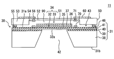
- FIG. 3 is a sectional view of the sensor unit taken along line III-III in FIG. 2.
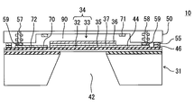
- FIG. 4 is a sectional view of the sensor unit taken along line IV-IV in FIG. 2.
- It is a block diagram which shows the outline of the circuit structure of an ultrasonic sensor apparatus. It is a flowchart which shows a transmission / reception process.
- the thickness direction of the substrate in other words, the vibration direction of the membrane structure is simply referred to as the thickness direction
- the direction perpendicular to the thickness direction is simply referred to as the vertical direction.
- the ultrasonic sensor device 10 includes a sensor unit 11 having an ultrasonic sensor 30 and a cover 50, and a circuit chip 12 in which a processing circuit 110 is configured in the same wiring board 13. To be implemented. A through-hole 13 a is formed in the wiring board 13 so that the ultrasonic sensor 30 can transmit and receive.
- the sensor unit 11 is fixed to a piezoelectric ultrasonic sensor 30 (sensor chip) manufactured using the MEMS technology, and a substrate 31 constituting the ultrasonic sensor 30,
- the cover 50 which forms the sealed space 90 between the substrates 31 is provided.
- the electrodes 70 and 71 for adjustment formed in each of the ultrasonic sensor 30 and the cover 50 are provided so that it may mutually oppose.
- the ultrasonic sensor 30 includes a substrate 31 having a thin portion 32 and a piezoelectric vibrator 33 formed on the thin portion 32 of the substrate 31.
- the thin-walled portion 32 and the piezoelectric vibrator 33 constitute a membrane structure 34 having a lower rigidity than other portions (thick-walled portion 43) of the substrate 31.
- the membrane structure 34 vibrates in the thickness direction, whereby ultrasonic waves are transmitted and received.
- an SOI structure substrate in which an insulating layer 39 made of silicon dioxide is interposed between a support substrate 38 made of silicon and a semiconductor layer 40 made of silicon, and a surface of the semiconductor layer 40 opposite to the insulating layer 39.
- a substrate 31 is constituted by the insulating film 41 formed thereon.
- the insulating film 41 a single layer film or a multilayer film made of silicon dioxide, silicon nitride, or the like can be used.
- the surface opposite to the semiconductor layer 40 in the insulating film 41 forms one surface 31a on which the piezoelectric vibrator 33 is formed, and the surface opposite to the insulating layer 39 in the support substrate 38 is the back surface 31b of the one surface 31a.
- an opening 42 is formed which has a surface opposite to the insulating film 41 in the semiconductor layer 40 as a bottom surface and opens to the back surface 31 b.
- the opening 42 is formed by partially removing the support substrate 38 and the insulating layer 39 by etching.
- the back surface 31b of the substrate 31 is the (100) plane
- the opening wall surface of the support substrate 38 is the (111) plane.
- the portion of the substrate 31 that crosslinks the opening 42 forms the thin portion 32 of the substrate 31.
- 3 is one surface of the thin portion 32 opposite to the piezoelectric vibrator 33, and this one surface 32a coincides with the surface forming the bottom of the opening 42 in the semiconductor layer 40 described above. Yes.
- a portion of the substrate 31 excluding the thin portion 32 forms a thick portion 43 of the substrate 31.
- the thin portion 32 has a planar rectangular outline
- the thick portion 43 has a rectangular ring shape so as to surround the thin portion 32.
- the piezoelectric vibrator 33 is formed on the one surface 31 a of the substrate 31 and in the thin portion 32. More specifically, as shown in FIG. 2, it is formed so as to form a planar rectangular shape slightly larger than the thin portion so as to cover the entire area of the thin portion 32.
- the piezoelectric vibrator 33 includes a piezoelectric thin film 37 disposed between a pair of detection electrodes 35 and 36.
- the piezoelectric thin film 37 corresponds to the piezoelectric body recited in the claims.
- the detection electrodes 35 and 36 face each other in the thickness direction. That is, in the thickness direction, the detection electrode 35, the piezoelectric thin film 37, and the detection electrode 36 are stacked in this order on the one surface 31 a of the substrate 31.
- platinum (Pt), gold (Au), aluminum (Al), or the like can be employed as a constituent material of the detection electrodes 35 and 36.
- ferroelectric PZT, aluminum nitride (AlN), zinc oxide (ZnO), or the like can be used. In the present embodiment, Pt is adopted as the constituent material of the detection electrodes 35 and 36, and PZT is adopted as the constituent material of the piezoelectric thin film 37.
- the reference numeral 44 shown in FIGS. 2 and 4 is a wiring for electrically connecting a pad (not shown) of the cover 50 and the detection electrode 35.
- reference numeral 45 shown in FIG. 2 is a wiring for electrically connecting a pad (not shown) of the cover 50 and the detection electrode 36. In the present embodiment, these wirings 44 and 45 are integrally formed using the same material as the detection electrodes 35 and 36.
- a metal layer 46 for fixing the cover 50 to the substrate 31 is formed on the thick portion 43 on the one surface 31 a of the substrate 31. As shown in FIG. 2, the metal layer 46 is formed in the vicinity of the outer peripheral end of the one surface 31a of the substrate 31 so as to surround the membrane structure 34, the wirings 44 and 45, and the adjustment electrodes 70 and 71.
- the cover 50 is fixed to the substrate 31 of the ultrasonic sensor 30 and forms a sealed space 90 adjacent to the membrane structure 34 between the cover 31 and the substrate 31.
- a synthetic resin a semiconductor such as silicon, or ceramic can be employed.
- a cover 50 made of synthetic resin is employed.
- the cover 50 is arranged such that a portion including at least a facing portion 51 that is disposed away from the membrane structure 34 in the thickness direction is displaced toward the membrane structure 34 by electrostatic attraction described later. It has become.
- the central portion including the facing portion 51 is thinner than the peripheral portion surrounding the central portion.
- this thin portion is referred to as a thin portion 52
- the peripheral thick portion is referred to as a thick portion 53.
- the thin portion 52 is larger than the thin portion 32 and thus the membrane structure 34, and the portion excluding the facing portion 51 faces the thick portion 43 of the substrate 31.
- the cover 50 made of synthetic resin and having different thicknesses between the thin wall portion 52 and the thick wall portion 53 is obtained by partially laminating and bonding a plurality of thermoplastic resin films having a predetermined thickness.
- the thickness of the part 52 and the thick part 53 is varied.
- the cover 50 is disposed on the one surface 31a side of the substrate 31 so that the concave portion 54 having the thin-walled portion 52 as a bottom portion is on the sealed space 90 side.
- a metal layer 55 is formed on the surface of the thick portion 53 facing the substrate 31 so as to face the metal layer 46 described above. That is, it is formed so as to surround the membrane structure 34, the wirings 44 and 45, and the adjustment electrodes 70 and 71. And metal layers 46 and 55 are joined together and the annular joined part is formed. With this joint, a sealed space 90 is formed between the cover 50 and the substrate 31. In the present embodiment, air is sealed in the sealed space 90 at atmospheric pressure.
- the cover 50 is provided with through electrodes for electrically connecting the detection electrodes 35 and 36 constituting the piezoelectric vibrator 33 and the adjustment electrodes 70 and 71 described later to the outside of the sealed space 90.
- Reference numeral 56 shown in FIG. 3 is a through electrode that is formed in a portion different from the facing portion 51 in the thin portion 52 and is electrically connected to the adjustment electrode 71 on the cover 50 side.
- Reference numeral 57 shown in FIG. 4 is a through electrode formed in the thick portion 53 and electrically connected to the adjustment electrode 70 on the ultrasonic sensor 30 side.
- Reference numeral 58 denotes a through electrode formed in the thick portion 53 and electrically connected to the detection electrode 35 (wiring 44) of the piezoelectric vibrator 33.
- a through-hole electrode electrically connected to the detection electrode 36 (wiring 45) is also formed in the thick portion 53 of the cover 50.
- Such through electrodes 56 to 58 can be formed by forming a through hole in a resin film and then filling the through hole with a conductive paste or metal plating.
- a wiring 60 is formed on the outer surface of the cover 50, one end of which is connected to the through electrode 56 and the other end is extended to the thick portion 53.
- the end of the wiring 60 on the thick portion 53 side is a pad (not shown), and for example, a bonding wire is connected to the pad.
- symbol 59 shown in FIG. 4 is the land formed in the opposing surface with the board
- FIG. This land is formed by patterning a copper foil, for example.
- the adjustment electrode 70 is electrically connected (soldered) to the through electrode 57 via the wiring 72 and the land 59.
- the detection electrode 35 is electrically connected (soldered) to the through electrode 58 via the wiring 44 and the land 59.
- the cover 50 formed by laminating a plurality of resin films includes the through electrodes 56 to 58, the land 59, the wiring 60, and the like. That is, the cover 50 is configured as a wiring board.
- the wiring 72 is a wiring that connects the adjustment electrode 70 and the through electrode 57 (land 59).
- the pair of adjustment electrodes 70, 71 fulfills the function of generating electrostatic attraction by energization and bringing the thin portion 52 (opposing portion 51) of the cover 50 closer to the membrane structure 34 of the ultrasonic sensor 30.
- the adjustment electrode 70 is formed on the ultrasonic sensor 30 side, and the adjustment electrode 71 is formed on the cover 50 at a position facing the adjustment electrode 70.
- the adjustment electrode 70 on the ultrasonic sensor 30 side is configured as a separate electrode from the detection electrodes 35 and 36 constituting the piezoelectric vibrator 33, and is formed on the thick portion 43 on the one surface 31 a of the substrate 31. It is formed so as to surround the membrane structure 34. More specifically, it is formed along the outer contour of the membrane structure 34 while having a predetermined clearance in the vertical direction with respect to the membrane structure 34, and has a substantially C-shape for drawing out the wires 44 and 45. is doing.
- the detection electrodes 35 and 36 and the wirings 44 and 45 are made of the same metal material.
- the adjustment electrode 71 on the cover 50 side is formed on the inner surface (the surface on the concave portion 54 side) of the thin portion 52 in the cover 50. More specifically, the thin portion 52 is formed in a portion outside the membrane structure 34 in the vertical direction.
- the adjustment electrode 71 has a rectangular ring shape because it is not necessary to draw out the wires 44 and 45. In the present embodiment, like the land 59, the copper foil is patterned.
- the thin-walled portion 32 of the substrate 31 and the piezoelectric vibrator 33 form a membrane structure 34 that is thinner than other portions, and the membrane structure 34 can vibrate in the thickness direction. It has become. Further, a sealed space 90 is formed between the substrate 31 and the cover 50 by the cover 50 fixed to the one surface 31 a of the substrate 31. For this reason, transmission / reception of ultrasonic waves is not performed on the side 31a of the substrate 31 on which the cover 50 is disposed, but transmission / reception of ultrasonic waves is performed on the back surface 31b side of the substrate 31.
- the processing circuit 110 includes a control circuit 111, a drive signal generation circuit 112, a drive circuit 113, an amplifier circuit 114, a filter circuit 115, a TAD 116, a DSP 117, and an adjustment voltage generation circuit 118.
- the processing circuit 110 corresponds to a control unit described in the claims.
- the control circuit 111 includes a central processing unit (CPU) (not shown), a read-on memory (ROM) in which various programs executed by the CPU are stored, and operations for various calculations that the CPU executes in accordance with the programs stored in the ROM.
- a random access memory (RAM) used as an area is provided.
- the drive signal generation circuit 112 has a function for controlling the timing of drive signal generation, a function for detecting the presence or absence of the subject and the position (distance and orientation) of the subject, a function for outputting the detection result to an external device, and adjustment
- the voltage generation circuit 118 has a function of controlling the timing for generating the adjustment voltage.
- the drive signal generation circuit 112 When the drive signal generation circuit 112 receives the instruction signal from the control circuit 111, the drive signal generation circuit 112 generates a pulse signal having a reference frequency for a certain period, and generates a drive signal having a predetermined frequency f1 based on the pulse signal. Specifically, a drive signal having a predetermined frequency f1 that substantially matches the resonance frequency of the membrane structure 34 is generated.
- the drive circuit 113 is a drive circuit that drives the piezoelectric vibrator 33 by the drive signal output from the drive signal generation circuit 112, whereby the ultrasonic sensor 30 (sensor unit 11) has a predetermined frequency f1. Ultrasound is transmitted.
- the drive circuit 113 includes a power amplifier circuit such as a transformer.
- the amplification circuit 114 amplifies the signal received by the piezoelectric vibrator 33 and outputs the amplified reception signal to the filter circuit 115.
- the filter circuit 115 performs a filter process on the received signal of the piezoelectric vibrator 33 amplified by the amplifier circuit 114. In the present embodiment, frequency components outside the reception band of the membrane structure 34 are removed.
- the TAD 116 is a known time A / D conversion circuit
- the DSP (digital signal processor) 117 is based on the reception signal of the piezoelectric vibrator 33 A / D converted by the TAD 116, and the amplitude and phase of the reception signal. Is calculated. These calculation results are output to the control circuit 111.
- the DSP 117 has a memory.
- the adjustment voltage generation circuit 118 When the adjustment voltage generation circuit 118 receives the instruction signal from the control circuit 111, the adjustment voltage generation circuit 118 applies a predetermined voltage between the adjustment electrodes 70 and 71. Further, when the instruction signal from the control circuit 111 is received, the voltage applied between the adjustment electrodes 70 and 71 is turned off.
- the control circuit 111 instructs the drive signal generation circuit 112 to generate a drive signal.
- the drive signal generation circuit 112 generates a drive signal having a predetermined frequency f 1 and outputs the drive signal to the drive circuit 113.
- the output drive signal (voltage signal) is transmitted to the detection electrodes 35 and 36 of the piezoelectric vibrator 33 via the drive circuit 113.
- the piezoelectric vibrator 33 vibrates in the vertical direction (d31 direction of PZT), and thereby the membrane structure 34 vibrates in the thickness direction.
- the cover 50 is disposed on the one surface 31a side of the substrate 31 with respect to the ultrasonic sensor 30, ultrasonic waves are transmitted mainly from the back surface 31b side of the substrate 31 by this vibration.
- the frequency of this ultrasonic wave coincides with the frequency f1 of the drive signal.
- the control circuit 111 instructs the adjustment voltage generation circuit 118 to generate the adjustment voltage.
- the adjustment voltage generation circuit 118 applies a predetermined voltage between the adjustment electrodes 70 and 71 (step 11).
- This step 11 corresponds to the voltage applying means described in the claims.
- the transmission process ends when the output of the drive signal from the drive signal generation circuit 112 is stopped, and as shown in FIG. 7, the output of the drive signal is stopped and the adjustment voltage is turned on. Note that after the output of the drive signal is stopped, the end of the reverberation period of the membrane structure 34 may end the transmission process, and the adjustment voltage may be turned on.
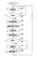
- step 11 when the adjustment voltage is applied to the adjustment electrodes 70 and 71, the control circuit 111 stores the amplitude of the received signal of the piezoelectric vibrator 33 calculated by the DSP 117 in advance in the memory of the DSP 117. It is compared whether it is larger than a predetermined threshold. That is, it is determined whether or not the ultrasonic sensor 30 (piezoelectric vibrator 33) has received the reflected wave (step 12).
- step 12 when the amplitude of the received signal of the piezoelectric vibrator 33 is larger than the threshold, the control circuit 111 determines that the subject exists (the subject is present), and from the timing when the amplitude exceeds the threshold, The distance to the subject is calculated (step 13).
- the control circuit 111 instructs the adjustment voltage generation circuit 118 to turn off the adjustment voltage.
- the adjustment voltage generation circuit 118 turns off the voltage application between the adjustment electrodes 70 and 71 (step 14).
- the adjustment voltage is applied at least in a period during which the piezoelectric vibrator 33 can receive the reflected wave, and the adjustment voltage is turned off until the next drive signal generation instruction.
- the cover 50 is fixed to the piezoelectric ultrasonic sensor 30, and a sealed space 90 in which air is sealed is formed between the substrate 31 and the cover 50.
- the sealed space 90 is adjacent to the membrane structure 34. As described above, the vibration of the membrane structure 34 is affected by the damping of the sealed space 90.
- the Q value indicating the vibration state of the membrane structure 34 is inversely proportional to the damping coefficient C of the sealed space 90 adjacent to the membrane structure 34, and the damping coefficient C depends on the facing portion 51 of the cover 50 and the membrane structure. 34 is inversely proportional to the facing distance D with respect to 34. For this reason, the damping coefficient C increases and the Q value decreases as the facing distance D decreases.
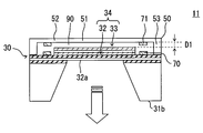
- the adjustment voltage is not applied to the adjustment electrodes 70 and 71 in the transmission state of the piezoelectric vibrator 33, that is, the period from the start of driving signal output to the stop of output or the period of stop of reverberation. For this reason, electrostatic attraction is not generated between the adjustment electrodes 70 and 71, and the facing portion 51 (thin portion 52) of the cover 50 does not approach the membrane structure 34 of the ultrasonic sensor 30 as shown in FIG. . Therefore, the facing distance between the facing portion 51 and the membrane structure 34 is the initial distance D1 when the membrane structure 34 is located at the center position of vibration, when ultrasonic waves are not transmitted and received and no adjustment voltage is applied. Is equal to
- an adjustment voltage is applied between the adjustment electrodes 70 and 71 in the reception state of the piezoelectric vibrator 33, that is, in a period during which the reflected wave can be received. For this reason, an electrostatic attractive force is generated between the adjustment electrodes 70 and 71, and the facing portion 51 (thin wall portion 52) of the cover 50 is deformed to the membrane structure 34 of the ultrasonic sensor 30 as shown in FIG. Gravitate. Accordingly, the facing distance between the facing portion 51 and the membrane structure 34 is D2, which is narrower than the initial distance D1, assuming that the membrane structure 34 is at the center position of vibration.
- the facing distance D2 in the reception state is narrower than the facing distance D1 in the transmission state. That is, the Q value in the reception state is set lower than the Q value in the transmission state. For this reason, as shown in FIG. 10, the frequency band of the membrane structure 34 in the transmission state and the frequency band of the membrane structure 34 in the reception state are wider in the reception state, although the amplitude peak is lower. .
- the resonance frequency of the membrane structure 34 is substantially the same between the transmission state and the reception state (at a predetermined resonance frequency f1). Match). That is, it is possible to suppress the shift of the resonance peak.
- the frequency band is narrow in the transmission state and the frequency band is wide in the reception state while the resonance frequency (resonance peak) is the same at f1. Therefore, even if the subject moves relatively and a Doppler shift occurs, it is possible to accurately detect the reflected wave, and thus the subject to be detected.
- the cover 50 is fixed to the one surface 31 a of the substrate 31, and the piezoelectric vibrator 33 is accommodated in the sealed space 90 formed between the cover 50 and the substrate 31. For this reason, the piezoelectric vibrator 33 can be protected by the cover 50.
- the adjustment electrode 70 on the ultrasonic sensor 30 side is formed on the thick portion 43 of the substrate 31. For this reason, even if electrostatic attraction occurs, the membrane structure 34 is unlikely to be deformed. Therefore, it is possible to effectively suppress the shift between the resonance frequency in the transmission state and the peak in the reception state.
- the adjustment electrode 70 on the ultrasonic sensor 30 side is formed on the one surface 31 a of the substrate 31.
- the process can be shared with the detection electrode 35, the wirings 44 and 45, and the manufacturing process can be simplified.
- the thickness of the thin portion 52 of the cover 50 is made thinner than the thick portion 53 surrounding the thin portion 52. For this reason, when electrostatic attraction occurs, the facing portion 51 of the cover 50 is deformed and tends to approach the membrane structure 34. Therefore, it is possible to more effectively suppress the shift between the resonance frequency in the transmission state and the peak in the reception state.
- the rigidity of the thin portion 52 of the cover 50 is lower than the rigidity of the membrane structure 34. For this reason, when the electrostatic attractive force is generated, the thin portion 52 of the cover 50 is more easily deformed than the membrane structure 34. Therefore, the cover 50 can be deformed by electrostatic attraction while the deformation of the membrane structure 34 is suppressed, and the facing distance D can be narrowed.
- the metal layer 46 formed on the one surface 31a of the substrate 31 and the metal layer 55 formed on the surface of the thick part 53 of the cover 50 are joined via solder or the like.
- the fixing of the cover 50 to the substrate 31 is not particularly limited to the above example. For example, it may be bonded and fixed. Further, when silicon is adopted as the constituent material of the cover 50, the cover 50 may be fixed to the silicon of the semiconductor layer 40 constituting the substrate 31 by direct bonding.
- an example in which an electrostatic attraction is generated by applying an adjustment voltage only when the membrane structure 34 is received is shown.
- an adjustment voltage may be applied to generate an electrostatic attractive force. Since the electrostatic attractive force is proportional to the square of the applied voltage, by setting the reception time higher than the transmission time, the reception interval D2 is narrower than the transmission interval D1. The Q value in the reception state can be made lower than the Q value in the transmission state.
- the adjustment voltage can be lowered by applying the adjustment voltage only when the membrane structure 34 is received.
- the thick portion 43 is annular and surrounds the thin portion 32 in the vertical direction.
- the thin portion 32 may be configured to bridge the two thick portions 43. In this case, at least a part of the cover 50 is fixed to the thin portion 32.
- the adjustment electrode 70 on the ultrasonic sensor 30 side is formed separately from the detection electrodes 35 and 36 of the piezoelectric vibrator 33 .
- one of the detection electrodes 35 and 36 of the piezoelectric vibrator 33 can also serve as the adjustment electrode 70 on the ultrasonic sensor 30 side.
- the detection electrode 36 close to the facing portion 51 in the thickness direction is also used as the adjustment electrode 70. According to this, since the adjustment electrode 70 is also used, the configuration of the sensor unit 11 and thus the ultrasonic sensor device 10 can be simplified.
- the membrane structure 34 is deformed by electrostatic attraction as compared with the configuration in which the adjustment electrode 70 is formed on the thick portion 43. It becomes easy to do.
- the adjustment electrode 71 on the cover 50 side is preferably formed at a position corresponding to the thick portion (43) of the substrate 31 in the vertical direction. According to this, the deformation due to the electrostatic attractive force of the membrane structure 34 can be suppressed while the adjustment electrode 70 is also used.
- the adjustment electrode 70 on the cover 50 side is provided to face the detection electrode 36 that also serves as the adjustment electrode 70, the rigidity of the facing portion 51 (thin portion 52) of the cover 50 including the adjustment electrode 70. Is lower than the rigidity of the membrane structure 34.
- the adjustment electrode 70 on the ultrasonic sensor 30 side has a substantially C shape by removing a part of the rectangular ring shape and the adjustment electrode 71 on the cover 50 side has a rectangular ring shape is shown.
- the adjustment electrode 70 on the ultrasonic sensor 30 side may be substantially C-shaped by removing a part of the circular ring, and the adjustment electrode 71 on the cover 50 side may be circular.
- the adjustment electrode 71 on the cover 50 side is shown to show the positional relationship.
- the adjustment electrode 70 on the ultrasonic sensor 30 side is formed in a C shape and is open (free end). An example in which the wirings 44 and 45 are drawn from the gap is shown.
- the adjustment electrode 70 can also be annular by using the wirings 44 and 45 as a lower layer wiring with respect to the adjustment electrode 70.
- the adjustment electrode 70 can be formed in a ring shape by using the wiring 72 or the adjustment electrode 70 and the wiring 72 as a lower layer wiring with respect to the wirings 44 and 45.
- the sealed gas is not particularly limited to air.
- a gas having a viscosity coefficient ⁇ larger than that of air may be enclosed.
- the damping coefficient C is proportional to the viscosity coefficient ⁇ of the sealed gas.
- the adjustment electrode 71 on the cover 50 side is provided on the inner surface (the surface facing the substrate 31) of the thin portion 52 of the cover 50 has been described.
- the adjustment electrode 71 may be provided on the outer surface of the thin portion 52. In this case, the configuration can be simplified.
- the cover 50 is fixed to the one surface 31 a of the substrate 31, and the piezoelectric vibrator 33 is accommodated in the sealed space 90.
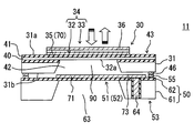
- the present embodiment is characterized in that the cover 50 is fixed to the back surface 31b of the substrate 31, as shown in FIG. For this reason, as shown in the first embodiment, ultrasonic waves are not transmitted / received on the back surface 31 b side of the substrate 31, but ultrasonic waves are transmitted / received on the one surface 31 a side of the substrate 31.
- the ultrasonic sensor 30 has substantially the same configuration as that shown in the first embodiment.
- the bonding metal layer 46 is formed on the back surface 31 b of the substrate 31 in the thick portion 43.
- the detection electrode 35 of the piezoelectric vibrator 33 also serves as the adjustment electrode 70 on the ultrasonic sensor 30 side.
- the cover 50 includes a semiconductor substrate 61 and an insulating film 62 formed on one surface of the semiconductor substrate 61.
- the cover 50 is formed with an opening 63 formed by removing at least the facing portion 51 of the semiconductor substrate 61 with the insulating film 62 as a bottom.
- the semiconductor substrate 61 is made of silicon, and the opening wall surface of the semiconductor substrate 61 is a (111) plane.
- a portion of the insulating film 62 that bridges the opening 63 forms a thin portion 52.
- the portion of the facing portion 51 is a thin portion 52.
- a metal layer 55 for bonding is formed on the thick portion 53 of the cover 50 on the surface opposite to the semiconductor substrate 61 in the insulating film 62.
- the metal layer 55 is bonded to the metal layer 46 of the ultrasonic sensor 30 described above, and the sealed space 90 including the opening 42 of the substrate 31 is formed by this bonding.
- the adjustment electrode 71 on the cover 50 side is formed on the surface of the insulating film 62 on which the metal layer 55 is formed, and on the facing portion 51.
- the adjustment electrode 71 is formed to be slightly larger than the facing portion 51 so as to cover the entire area of the facing portion 51 (thin portion 52) having a planar rectangular shape in the vertical direction.
- it is electrically connected to a through electrode 64 that penetrates the semiconductor substrate 61 and the insulating film 62 via a wiring 73.
- the facing portion 51 of the cover 50 includes the insulating film 62 and the adjustment electrode 71.
- the membrane structure 34 of the ultrasonic sensor 30 includes the thin portion 32 (semiconductor layer 40 and insulating film 41) of the substrate 31 and the piezoelectric vibrator 33, as in the first embodiment. For this reason, the rigidity of the facing portion 51 of the cover 50 including the adjustment electrode 70 is lower than the rigidity of the membrane structure 34.
- the detection electrode 35 also serves as the adjustment electrode 70
- the configuration of the sensor unit 11, and thus the ultrasonic sensor device 10 can be simplified.
- the detection electrode 36 may also serve as the adjustment electrode 70.
- the adjustment electrode 70 can be provided as an electrode different from the detection electrodes 35 and 36.
- the adjustment electrode 70 can be provided between the semiconductor layer 40 and the insulating film 41 or on the one surface 32 a of the thin portion 32. That is, there is no particular limitation as long as it is within the formation range of the membrane structure 34.
- cover 50 including the semiconductor substrate 61 and the insulating film 62 is shown, but the configuration of the cover 50 is not particularly limited to the above example.
- a resin cover 50 may be employed.
- the DSP 117 calculates the frequency of the received signal. Then, the control circuit 111 calculates the difference between the calculated frequency of the received signal and the frequency of the drive signal, that is, the frequency of the transmission signal, and generates an adjustment voltage so as to generate a predetermined voltage based on this frequency difference. It is characterized in that the circuit 118 is instructed.
- step 20 The transmission process in step 20 is the same as step 10 shown in the first embodiment (see FIG. 7).
- ultrasonic waves are transmitted from the one surface 31a side of the substrate 31 as described above.
- the frequency of this ultrasonic wave coincides with the frequency f1 of the drive signal.
- the control circuit 111 compares whether or not the amplitude of the received signal of the piezoelectric vibrator 33 calculated by the DSP 117 is larger than a predetermined threshold value stored in advance in the memory of the DSP 117. That is, it is determined whether or not the ultrasonic sensor 30 (piezoelectric vibrator 33) has received the reflected wave (step 21).
- step 21 if the amplitude of the received signal of the piezoelectric vibrator 33 is smaller than the threshold in a predetermined period in which the reflected wave can be received after generating the drive signal, steps 20 and 21 are executed again.
- the control circuit 111 calculates the frequency of the reception signal calculated by the DSP 117 and the frequency f1 of the drive signal stored in the memory of the control circuit 111.
- a frequency difference is calculated (step 22). This step 22 corresponds to the frequency difference calculating means described in the claims.
- the control circuit 111 determines a voltage value to be generated by the adjustment voltage generation circuit 118 from the calculated frequency difference (step 23).
- This step 23 corresponds to the voltage value determining main stage described in the claims. For example, a larger value is set as the adjustment voltage so that the Q value of the membrane structure 34 becomes lower as the frequency difference is larger, that is, as the Doppler shift amount is larger.
- an ultrasonic transmission process is executed as in S20 (step 24).
- the control voltage generation instruction signal is not output from the control circuit 111 to the adjustment voltage generation circuit 118.
- step 23 the control circuit 111 instructs the adjustment voltage generation circuit 118 to generate the adjustment voltage.
- an instruction is given to generate a predetermined voltage value determined in the processing of steps 20 to 23.
- the adjustment voltage generation circuit 118 applies a predetermined voltage between the adjustment electrodes 70 and 71 (step 25).
- This step 25 corresponds to the voltage applying means described in the claims.
- Subsequent steps 26 to 28 are the same as steps 12 to 14 shown in the first embodiment.
- the voltage value of the adjustment voltage applied to the adjustment electrodes 70 and 71 is determined based on the difference between the transmission frequency and the frequency of the received reflected wave. That is, the Q value of the reception state is set according to the movement state (for example, speed) of the subject that moves relatively. For this reason, the subject can be detected with high accuracy regardless of the relative movement state of the subject.
- the flow shown in FIG. 14 shows an example in which the processing of steps 20 to 23 is executed every time the processing of steps 24 to 28 is executed once.
- the processing in steps 24 to 28 may be repeatedly executed in a predetermined period. That is, the transmission / reception processing may be executed a plurality of times using the determined adjustment voltage value.
- the processing circuit 110 applies a voltage between the adjustment electrodes 70 and 71, and changes the facing distance D between the facing portion 51 of the cover 50 and the membrane structure 34 by electrostatic force, whereby the membrane structure.
- the Q value of the body 34 is changed. That is, the adjustment electrodes 70 and 71 function as Q value varying means.
- the Q value variable means is not limited to the above embodiment.
- a film 200 having a thermal expansion coefficient different from that of the cover 50 is provided on the upper surface of the cover 50, and an electric current is passed through the cover 50 or the film 200 to generate heat.
- the cover 50 bends due to the difference in thermal expansion coefficient between the cover 50 and the membrane 200, and the facing distance D is changed. That is, the film 200 functions as a Q value variable means.
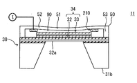
- the piezoelectric body 210 is fixed to the inner surface of the cover 50, and the piezoelectric body 200 is distorted by passing a current through the piezoelectric body 210. As a result, the cover 50 is bent and the facing distance D is changed. That is, the piezoelectric body 210 functions as a Q value variable means.
- the cam 220 is provided on the upper portion of the cover 50.
- the cam 220 is in contact with the upper surface of the cover 50 at a predetermined rotation angle.
- the cover 50 is bent and the facing distance D is changed. That is, the cam 220 functions as a Q value variable means.
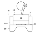
- the roof portion of the cover 50 is removed, and the piston 230 is arranged so as to slide with the side surface of the cover 50 to form the sealed space 90.
- the distance between the lower surface of the piston 230 and the membrane structure 34 is the facing distance D, and the facing distance D is changed as the piston 230 moves up and down. That is, the piston 230 functions as a Q value variable means.
- a through hole is formed in the roof portion of the cover 50, and the pump 240 is connected to the sealed space 90 through the through hole.
- the viscosity coefficient ⁇ of the gas in the sealed space 90 is changed.
- the damping coefficient C of the sealed space 90 is proportional to the viscosity coefficient ⁇ of the gas sealed in the sealed space 90. Therefore, the damping coefficient C of the sealed space 90 can be changed by changing the pressure or temperature in the sealed space 90.
- the Q value of the membrane structure 34 is changed. That is, the pump 240 functions as a Q value variable means.
- the damping coefficient C of the sealed space 90 and consequently the Q value of the membrane structure 34 can be changed by replacing the gas in the sealed space 90 with the pump 240.
- a first gas for example, air
- a second gas for example, helium
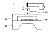
- the magnet 250 is fixed to the upper surface of the cover 50, and a magnetic field is generated around the magnet 250 by passing a current through a coil arranged in the vicinity. As a result, the cover 50 is bent and the facing distance D is changed. That is, the magnet 250 functions as a Q value variable means.
- a hydraulic diaphragm pump is configured by the cover 50 and the diaphragm 260, and the gas pressure and temperature of the sealed space 90 are changed. That is, the diaphragm 260 functions as a Q value variable means.
- the Q value of the membrane structure 34 is changed by changing the facing distance D or changing the viscosity coefficient of the gas in the sealed space 90.
- the member functions as a Q value variable means.
Landscapes
- Engineering & Computer Science (AREA)
- Physics & Mathematics (AREA)
- Radar, Positioning & Navigation (AREA)
- Remote Sensing (AREA)
- Computer Networks & Wireless Communication (AREA)
- General Physics & Mathematics (AREA)
- Acoustics & Sound (AREA)
- Mechanical Engineering (AREA)
- Signal Processing (AREA)
- Transducers For Ultrasonic Waves (AREA)
- Measurement Of Velocity Or Position Using Acoustic Or Ultrasonic Waves (AREA)
- Ultra Sonic Daignosis Equipment (AREA)
- Investigating Or Analyzing Materials By The Use Of Ultrasonic Waves (AREA)
Abstract
Description
図1に示すように、本実施形態に係る超音波センサ装置10は、超音波センサ30及びカバー50を有するセンサユニット11と、処理回路110が構成された回路チップ12が、同一の配線基板13に実装されてなる。配線基板13には、超音波センサ30が送受信可能なように、貫通孔13aが形成されている。
本実施形態では、超音波センサ装置10が、センサユニット11とは別に回路チップ12及び配線基板13を有する例を示した。しかしながら、回路チップ12に構成される処理回路110がセンサユニット11に形成された構成(集積された構成)を採用することもできる。
第1実施形態では、基板31の一面31aにカバー50が固定され、圧電振動子33が密閉空間90に収容される例を示した。これに対し、本実施形態では、図13に示すように、基板31の裏面31bにカバー50が固定される点を特徴とする。このため、第1実施形態に示すように、基板31の裏面31b側で超音波の送受信がなされるのではなく、基板31の一面31a側で超音波の送受信がなされる。
第1実施形態では、受信時において、予め設定された所定電圧を調整用電圧として調整用電極70,71間に印加する例を示した。これに対し、本実施形態では、受信信号の周波数をDSP117が算出する。そして、制御回路111は、算出された受信信号の周波数と、駆動信号の周波数、すなわち送信信号の周波数との差を算出し、この周波数差に基づく所定電圧を生成するように、調整用電圧生成回路118に指示する点を特徴とする。
(他の実施形態)
本開示は、実施例に準拠して記述されたが、本開示は当該実施例や構造に限定されるものではないと理解される。本開示は、様々な変形例や均等範囲内の変形をも包含する。加えて、様々な組み合わせや形態、さらには、それらに一要素のみ、それ以上、あるいはそれ以下、を含む他の組み合わせや形態をも、本開示の範疇や思想範囲に入るものである。
Claims (17)
- 基板(31)と、
前記基板(31)の厚さ方向において対向配置された一対の検出用電極(35,36)間に圧電体(37)が介在されてなり、前記基板(31)の一面(31a)上に形成されて、前記基板(31)の他の部分よりも剛性の低いメンブレン構造体(34)を構成する圧電振動子(33)と、を有し、
前記圧電振動子(33)により超音波を送信するととともに、同一の前記圧電振動子(33)によりその反射波を受信する超音波センサ(30)を備えた超音波センサ装置であって、
前記圧電振動子(33)が超音波を送信する送信期間の当該圧電振動子(33)のQ値を、前記圧電振動子(33)が超音波を受信する受信期間の当該圧電振動子(33)のQ値よりも大きくするQ値可変手段(70,71、110、200,210,220,230,240,250,260)を有する超音波センサ装置。 - 前記基板(31)の厚さ方向において、前記メンブレン構造体(34)と離間しつつ対向して配置された対向部(51)を有し、前記基板(31)に固定されて、前記基板(31)との間に気体が封入された密閉空間(90)を形成するカバー(50)を備え、
前記Q値可変手段(70,71、110、200,210,220,230,250)は、前記対向部(51)と前記メンブレン構造体(34)とのギャップ間隔を可変することで、前記圧電振動子(33)が超音波を送信する送信期間の当該圧電振動子(33)のQ値を、前記圧電振動子(33)が超音波を受信する受信期間の当該圧電振動子(33)のQ値よりも大きくする請求項1に記載の超音波センサ装置。 - 前記Q値可変手段は、一方が前記超音波センサ(30)に形成され、他方が前記カバー(50)に形成されて前記基板(31)の厚さ方向において対向配置され、通電により静電引力を生じる一対の調整用電極(70,71)と、
前記調整用電極(70,71)への通電を制御する制御部(110)と、を備え、
前記静電引力により、前記カバー(50)の対向部(51)が前記メンブレン構造体(34)に近づくように構成され、
前記制御部(110)は、少なくとも前記圧電振動子(33)の受信状態で前記調整用電極(70,71)間に電圧を印加するとともに、前記圧電振動子(33)の受信状態における前記カバー(50)の対向部(51)と前記メンブレン構造体(34)との対向間隔(D2)のほうが、前記圧電振動子(33)の送信状態における前記カバー(50)の対向部(51)と前記メンブレン構造体(34)との対向間隔(D1)よりも狭くなるように前記調整用電極(70,71)への通電を制御する電圧印加手段(S11,S25)を有する請求項2に記載の超音波センサ装置。 - 前記基板(31)は、薄肉部(32)を有しており、
前記圧電振動子(33)は、前記基板(31)の一面(31a)であって前記薄肉部(32)上に形成されて、前記薄肉部(32)とともに前記メンブレン構造体(34)を構成している請求項1に記載の超音波センサ装置。 - 前記カバー(50)は、前記基板(31)の一面(31a)に固定され、
前記カバー(50)と前記基板(31)との間に形成される密閉空間(90)に、前記圧電振動子(33)が収容される請求項2に記載の超音波センサ装置。 - 前記超音波センサ側の調整用電極(70)は、前記基板(31)において前記薄肉部(32)とは異なる厚肉部(43)に形成される請求項4に記載の超音波センサ装置。
- 前記基板(31)の厚さ方向に垂直な方向において、前記厚肉部(43)は環状とされて前記薄肉部(32)を取り囲んでいる請求項6に記載の超音波センサ装置。
- 前記超音波センサ側の調整用電極(70)は、前記基板(31)の一面(31a)上に形成される請求項3に記載の超音波センサ装置。
- 前記カバー(50)において、前記対向部(51)と前記調整用電極(71)の形成部分とを含む中央部分(52)が、該中央部分(52)に隣接する周辺部分(53)よりも薄い請求項3に記載の超音波センサ装置。
- 前記カバー側の調整用電極(70)を含むカバー(50)の中央部分(52)の剛性が、前記メンブレン構造体(34)の剛性よりも低い請求項9に記載の超音波センサ装置。
- 前記圧電振動子(33)の検出用電極(35,36)の一方が、前記超音波センサ側の調整用電極(70)を兼ねており、
前記カバー側の調整用電極(71)は、前記基板(31)の厚さ方向に垂直な方向において、前記基板(31)における薄肉部(32)とは異なる厚肉部(43)に対応して形成される請求項3に記載の超音波センサ装置。 - 前記カバー(50)は、前記基板(31)における一面(31a)と反対の面(31b)に固定され、前記対向部(51)は、前記薄肉部(32)における圧電振動子(33)が形成された面と反対の面(32a)に対向しており、
前記カバー側の調整用電極(71)は、前記対向部(51)に形成され、
前記超音波センサ側の調整用電極(70)は、前記メンブレン構造体(34)に形成され、
前記カバー側の調整用電極(71)を含むカバー(50)の対向部(51)の剛性が、前記メンブレン構造体(34)の剛性よりも低い請求項3に記載の超音波センサ装置。 - 前記圧電振動子(33)の検出用電極(35,36)の一方が、前記超音波センサ側の調整用電極(70)を兼ねる請求項12に記載の超音波センサ装置。
- 前記密閉空間(90)に空気が封入されている請求項2~13いずれか1項に記載の超音波センサ装置。
- 前記密閉空間(90)に、空気よりも粘性係数の大きい気体が封入されている請求項2~13いずれか1項に記載の超音波センサ装置。
- 前記電圧印加手段(S11,S25)は、前記圧電振動子(33)の受信状態のみ、前記調整用電極(70,71)に電圧を印加する請求項3に記載の超音波センサ装置。
- 前記制御部(110)は、
前記調整用電極(70,71)に電圧を印加しない状態で、前記圧電振動子(33)が送信する超音波の周波数と、送信した超音波の反射波の周波数との差を算出する周波数差算出手段(S22)と、
前記周波数差算出手段により算出された周波数差により、前記調整用電極(70,71)に印加する電圧値を決定する電圧値決定手段(S23)と、を有し、
前記電圧印加手段(S25)は、前記電圧値決定手段(S23)にて決定された電圧値を前記調整用電極(70,71)に印加する請求項16に記載の超音波センサ装置。
Priority Applications (3)
| Application Number | Priority Date | Filing Date | Title |
|---|---|---|---|
| US14/117,050 US9348027B2 (en) | 2011-06-13 | 2012-06-12 | Ultrasonic sensor device |
| CN201280029347.8A CN103597854B (zh) | 2011-06-13 | 2012-06-12 | 超声波传感器装置 |
| DE112012002438.9T DE112012002438T5 (de) | 2011-06-13 | 2012-06-12 | Ultraschallsensorvorrichtung |
Applications Claiming Priority (2)
| Application Number | Priority Date | Filing Date | Title |
|---|---|---|---|
| JP2011131411A JP5327279B2 (ja) | 2011-06-13 | 2011-06-13 | 超音波センサ装置 |
| JP2011-131411 | 2011-06-13 |
Publications (1)
| Publication Number | Publication Date |
|---|---|
| WO2012172775A1 true WO2012172775A1 (ja) | 2012-12-20 |
Family
ID=47356782
Family Applications (1)
| Application Number | Title | Priority Date | Filing Date |
|---|---|---|---|
| PCT/JP2012/003802 Ceased WO2012172775A1 (ja) | 2011-06-13 | 2012-06-12 | 超音波センサ装置 |
Country Status (5)
| Country | Link |
|---|---|
| US (1) | US9348027B2 (ja) |
| JP (1) | JP5327279B2 (ja) |
| CN (1) | CN103597854B (ja) |
| DE (1) | DE112012002438T5 (ja) |
| WO (1) | WO2012172775A1 (ja) |
Cited By (2)
| Publication number | Priority date | Publication date | Assignee | Title |
|---|---|---|---|---|
| JP2014194993A (ja) * | 2013-03-28 | 2014-10-09 | Seiko Epson Corp | 圧電素子モジュール、超音波トランスデューサー、超音波デバイス、液体噴射ヘッド、液体噴射装置及び圧電素子モジュールの製造方法 |
| CN104730525A (zh) * | 2013-12-18 | 2015-06-24 | 精工爱普生株式会社 | 超声波传感器及其制造方法以及使用该超声波传感器的测量方法 |
Families Citing this family (25)
| Publication number | Priority date | Publication date | Assignee | Title |
|---|---|---|---|---|
| JP6284076B2 (ja) * | 2013-11-22 | 2018-02-28 | 国立大学法人豊橋技術科学大学 | 物理・化学センサおよび特定物質の測定方法 |
| JP6458934B2 (ja) * | 2013-12-18 | 2019-01-30 | セイコーエプソン株式会社 | 超音波センサー |
| JP6587051B2 (ja) | 2015-03-24 | 2019-10-09 | セイコーエプソン株式会社 | 超音波センサー及びその製造方法 |
| CN104809431B (zh) * | 2015-04-03 | 2018-04-27 | 业成光电(深圳)有限公司 | 超声波感测装置 |
| JP6672877B2 (ja) * | 2016-02-22 | 2020-03-25 | セイコーエプソン株式会社 | 超音波デバイス、超音波プローブ、超音波装置、及び超音波デバイスの製造方法 |
| WO2017188125A1 (ja) * | 2016-04-27 | 2017-11-02 | セイコーエプソン株式会社 | 実装構造体、超音波デバイス、超音波探触子、超音波装置、及び電子機器 |
| CN106269452B (zh) * | 2016-08-26 | 2018-12-18 | 北京七星华创电子股份有限公司 | 一种组合式多频率超声波/兆声波清洗装置 |
| CN106238302B (zh) * | 2016-08-26 | 2018-10-16 | 北京七星华创电子股份有限公司 | 一种频率动态变化的超声波/兆声波清洗装置 |
| US10545581B2 (en) * | 2017-10-05 | 2020-01-28 | Advanced Semiconductor Engineering, Inc. | Semiconductor package device |
| CN108267102B (zh) * | 2018-01-03 | 2019-12-27 | 京东方科技集团股份有限公司 | 一种段差检测设备及段差检测方法 |
| JP7091699B2 (ja) * | 2018-02-21 | 2022-06-28 | セイコーエプソン株式会社 | 超音波センサー、超音波装置、及び超音波センサーの製造方法 |
| EP3905716B1 (en) * | 2018-12-26 | 2023-10-04 | Sony Group Corporation | Ultrasound device |
| JP7211220B2 (ja) * | 2019-04-05 | 2023-01-24 | 株式会社デンソー | 超音波センサ |
| US10805751B1 (en) * | 2019-09-08 | 2020-10-13 | xMEMS Labs, Inc. | Sound producing device |
| JP7486030B2 (ja) * | 2020-01-21 | 2024-05-17 | セイコーエプソン株式会社 | 超音波デバイス及び超音波デバイスの製造方法 |
| DE102020200771B4 (de) | 2020-01-23 | 2023-03-30 | Vitesco Technologies Germany Gmbh | Fluidsensorvorrichtung zum Erfassen des Füllstands und/oder der Qualität eines Fluids und Verfahren zum Herstellen derselben |
| DE102020008069B4 (de) | 2020-07-21 | 2022-02-10 | Elmos Semiconductor Se | Ultraschallmessvorrichtung unter Nutzung eines Referenzspektrums |
| DE102020008067B4 (de) | 2020-07-21 | 2022-02-10 | Elmos Semiconductor Se | Ultraschallmessvorrichtung mit piezoresitivem MEMS-Empfänger und piezoelektrischem Schwingelement |
| DE102020119242B4 (de) * | 2020-07-21 | 2022-02-10 | Elmos Semiconductor Se | Ultraschallmessvorrichtung zur Verwendung von Dirac-Pulsen im Frequenzbereich für die Erfassung der Struktur des Umfelds einer mobilen Vorrichtung |
| DE102020008068B4 (de) | 2020-07-21 | 2022-02-10 | Elmos Semiconductor Se | MEMS-basierende Ultraschallmessvorrichtung unter Nutzung eines Referenzspektrums |
| CN112305074B (zh) * | 2020-10-28 | 2023-05-23 | 济南大学 | 一种水泥混凝土水化进程在线监测的压电超声装置 |
| WO2023044841A1 (zh) * | 2021-09-26 | 2023-03-30 | 京东方科技集团股份有限公司 | 触觉再现设备、方法、显示装置和控制器 |
| DE102021131711A1 (de) * | 2021-12-02 | 2023-06-07 | Valeo Schalter Und Sensoren Gmbh | Ultraschallsensor, kraftfahrzeug und verfahren zum betreiben des ultraschallsensors |
| TW202340753A (zh) * | 2022-01-17 | 2023-10-16 | 日商Cast股份有限公司 | 鬆動檢測系統及感測器基材 |
| DE102024204615A1 (de) * | 2024-05-17 | 2025-11-20 | Robert Bosch Gesellschaft mit beschränkter Haftung | Ultraschallsensor |
Citations (5)
| Publication number | Priority date | Publication date | Assignee | Title |
|---|---|---|---|---|
| JPH03133300A (ja) * | 1989-10-19 | 1991-06-06 | Fuji Electric Co Ltd | 複合圧電型超音波探触子 |
| JP2000253494A (ja) * | 1999-02-26 | 2000-09-14 | Nippon Soken Inc | 超音波センサ用圧電素子 |
| JP2001258879A (ja) * | 2000-03-15 | 2001-09-25 | Olympus Optical Co Ltd | 超音波トランスデューサシステムおよび超音波トランスデュー |
| JP2002188946A (ja) * | 2000-12-21 | 2002-07-05 | Murata Mfg Co Ltd | 超音波センサ |
| JP2006094459A (ja) * | 2004-08-25 | 2006-04-06 | Denso Corp | 超音波センサ |
Family Cites Families (19)
| Publication number | Priority date | Publication date | Assignee | Title |
|---|---|---|---|---|
| US3139603A (en) * | 1960-12-29 | 1964-06-30 | Acoustica Associates Inc | Mass-loaded electromechanical transducer |
| JPS5728500A (en) | 1980-07-29 | 1982-02-16 | Kureha Chem Ind Co Ltd | Ultrasonic wave transducer |
| DE3422115A1 (de) | 1984-06-14 | 1985-12-19 | Siemens AG, 1000 Berlin und 8000 München | Ultraschallwandlersystem |
| JP2961198B2 (ja) | 1989-01-27 | 1999-10-12 | 本多電子株式会社 | 周波数可変振動子 |
| JPH0618033A (ja) | 1991-09-21 | 1994-01-25 | Toho Seisakusho:Kk | レーザ式点火方法 |
| JP3285140B2 (ja) * | 1997-09-04 | 2002-05-27 | 株式会社村田製作所 | 振動ジャイロの調整方法 |
| US6443900B2 (en) | 2000-03-15 | 2002-09-03 | Olympus Optical Co., Ltd. | Ultrasonic wave transducer system and ultrasonic wave transducer |
| CN100544500C (zh) * | 2002-01-30 | 2009-09-23 | 松下电器产业株式会社 | 超高频再生用扬声器 |
| JP2003284182A (ja) | 2002-03-25 | 2003-10-03 | Osaka Industrial Promotion Organization | 超音波センサ素子と超音波アレイセンサ装置とそれらの共振周波数の調整方法 |
| JP4192672B2 (ja) * | 2003-05-16 | 2008-12-10 | 株式会社日本自動車部品総合研究所 | 超音波センサ |
| JP4254411B2 (ja) | 2003-07-31 | 2009-04-15 | パナソニック電工株式会社 | 圧電型超音波センサ |
| WO2005084284A2 (en) * | 2004-02-27 | 2005-09-15 | Georgia Tech Research Corporation | Multiple element electrode cmut devices and fabrication methods |
| JP4715236B2 (ja) * | 2005-03-01 | 2011-07-06 | 株式会社デンソー | 超音波センサ装置 |
| JP5145637B2 (ja) * | 2005-03-04 | 2013-02-20 | ソニー株式会社 | 振動型ジャイロセンサ |
| US8105941B2 (en) * | 2005-05-18 | 2012-01-31 | Kolo Technologies, Inc. | Through-wafer interconnection |
| JP2006332991A (ja) | 2005-05-25 | 2006-12-07 | Osaka Univ | 圧電共振型センサ素子の共振周波数の制御装置及び制御方法 |
| JP4983171B2 (ja) * | 2005-11-15 | 2012-07-25 | セイコーエプソン株式会社 | 静電型トランスデューサ、容量性負荷の駆動回路、回路定数の設定方法、超音波スピーカ、および指向性音響システム |
| US7730785B2 (en) | 2006-04-26 | 2010-06-08 | Denso Corporation | Ultrasonic sensor and manufacture method of the same |
| DE102009000348B4 (de) * | 2008-08-28 | 2011-09-01 | Schott Ag | Verfahren zur Herstellung von Flachglas |
-
2011
- 2011-06-13 JP JP2011131411A patent/JP5327279B2/ja not_active Expired - Fee Related
-
2012
- 2012-06-12 DE DE112012002438.9T patent/DE112012002438T5/de not_active Withdrawn
- 2012-06-12 US US14/117,050 patent/US9348027B2/en not_active Expired - Fee Related
- 2012-06-12 CN CN201280029347.8A patent/CN103597854B/zh not_active Expired - Fee Related
- 2012-06-12 WO PCT/JP2012/003802 patent/WO2012172775A1/ja not_active Ceased
Patent Citations (5)
| Publication number | Priority date | Publication date | Assignee | Title |
|---|---|---|---|---|
| JPH03133300A (ja) * | 1989-10-19 | 1991-06-06 | Fuji Electric Co Ltd | 複合圧電型超音波探触子 |
| JP2000253494A (ja) * | 1999-02-26 | 2000-09-14 | Nippon Soken Inc | 超音波センサ用圧電素子 |
| JP2001258879A (ja) * | 2000-03-15 | 2001-09-25 | Olympus Optical Co Ltd | 超音波トランスデューサシステムおよび超音波トランスデュー |
| JP2002188946A (ja) * | 2000-12-21 | 2002-07-05 | Murata Mfg Co Ltd | 超音波センサ |
| JP2006094459A (ja) * | 2004-08-25 | 2006-04-06 | Denso Corp | 超音波センサ |
Cited By (5)
| Publication number | Priority date | Publication date | Assignee | Title |
|---|---|---|---|---|
| JP2014194993A (ja) * | 2013-03-28 | 2014-10-09 | Seiko Epson Corp | 圧電素子モジュール、超音波トランスデューサー、超音波デバイス、液体噴射ヘッド、液体噴射装置及び圧電素子モジュールの製造方法 |
| CN104730525A (zh) * | 2013-12-18 | 2015-06-24 | 精工爱普生株式会社 | 超声波传感器及其制造方法以及使用该超声波传感器的测量方法 |
| EP2886210A3 (en) * | 2013-12-18 | 2016-01-13 | Seiko Epson Corporation | Ultrasonic sensor and measuring method using the same, and method of manufacturing ultrasonic sensor |
| US9772314B2 (en) | 2013-12-18 | 2017-09-26 | Seiko Epson Corporation | Ultrasonic sensor and measuring method using the same, and method of manufacturing ultrasonic sensor |
| US10161916B2 (en) | 2013-12-18 | 2018-12-25 | Seiko Epson Corporation | Ultrasonic sensor and measuring method using the same, and method of manufacturing ultrasonic sensor |
Also Published As
| Publication number | Publication date |
|---|---|
| CN103597854B (zh) | 2016-04-27 |
| DE112012002438T5 (de) | 2014-04-17 |
| US20140157902A1 (en) | 2014-06-12 |
| US9348027B2 (en) | 2016-05-24 |
| CN103597854A (zh) | 2014-02-19 |
| JP5327279B2 (ja) | 2013-10-30 |
| JP2013005040A (ja) | 2013-01-07 |
Similar Documents
| Publication | Publication Date | Title |
|---|---|---|
| JP5327279B2 (ja) | 超音波センサ装置 | |
| CN103097041B (zh) | 薄膜超声换能器 | |
| CN102859580B (zh) | 用于触发超声传感器的方法以及超声传感器 | |
| JP3944052B2 (ja) | 超音波送受波器及びこれを用いた超音波クリアランスソナー | |
| WO2011021358A2 (en) | Capacitive electromechanical transducer apparatus and method for adjusting its sensitivity | |
| JP7091699B2 (ja) | 超音波センサー、超音波装置、及び超音波センサーの製造方法 | |
| US11583896B2 (en) | Sound transducer including a piezoceramic transducer element integrated in a vibratory diaphragm | |
| JP2009260723A (ja) | トランスデューサ | |
| CN105073281A (zh) | 用于车辆的周围环境检测的传感器装置和方法 | |
| US20170160386A1 (en) | Ultrasonic sensor device for a motor vehicle, driver assistance system, and motor vehicle | |
| WO2021192417A1 (ja) | 超音波トランスデューサ | |
| JP7439728B2 (ja) | 超音波センサ | |
| JP2010216846A (ja) | センサデバイス | |
| CN113839582B (zh) | 具有有源阻尼器的微机电膜换能器 | |
| US11899143B2 (en) | Ultrasound sensor array for parking assist systems | |
| JP3259322B2 (ja) | 音波トランスデューサ | |
| US20230008879A1 (en) | Ultrasound transducer including a combination of a bending and piston mode | |
| JP2005331485A (ja) | 圧電素子および電気機械変換装置 | |
| WO2006126401A1 (ja) | 圧電共振型センサ素子の振動制御装置 | |
| JP7660664B2 (ja) | 超音波トランスデューサ、測距装置および超音波トランスデューサの製造方法 | |
| JP7699670B2 (ja) | 超音波トランスデューサの製造方法、超音波トランスデューサおよび測距装置 | |
| JP7453847B2 (ja) | 音波制御モジュール | |
| JP2004056450A (ja) | 超音波センサ | |
| JPH1175297A (ja) | 超音波マイクロホンおよびその周波数調整方法 | |
| JPH02248864A (ja) | 超音波トランスジューサ |
Legal Events
| Date | Code | Title | Description |
|---|---|---|---|
| WWE | Wipo information: entry into national phase |
Ref document number: 201280029347.8 Country of ref document: CN |
|
| 121 | Ep: the epo has been informed by wipo that ep was designated in this application |
Ref document number: 12799999 Country of ref document: EP Kind code of ref document: A1 |
|
| WWE | Wipo information: entry into national phase |
Ref document number: 14117050 Country of ref document: US |
|
| WWE | Wipo information: entry into national phase |
Ref document number: 1120120024389 Country of ref document: DE Ref document number: 112012002438 Country of ref document: DE |
|
| 122 | Ep: pct application non-entry in european phase |
Ref document number: 12799999 Country of ref document: EP Kind code of ref document: A1 |