WO2012169589A1 - 液晶表示装置及びその駆動方法 - Google Patents
液晶表示装置及びその駆動方法 Download PDFInfo
- Publication number
- WO2012169589A1 WO2012169589A1 PCT/JP2012/064688 JP2012064688W WO2012169589A1 WO 2012169589 A1 WO2012169589 A1 WO 2012169589A1 JP 2012064688 W JP2012064688 W JP 2012064688W WO 2012169589 A1 WO2012169589 A1 WO 2012169589A1
- Authority
- WO
- WIPO (PCT)
- Prior art keywords
- voltage
- period
- subframe
- liquid crystal
- driving
- Prior art date
- Legal status (The legal status is an assumption and is not a legal conclusion. Google has not performed a legal analysis and makes no representation as to the accuracy of the status listed.)
- Ceased
Links
Images






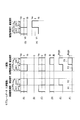


Classifications
-
- G—PHYSICS
- G09—EDUCATION; CRYPTOGRAPHY; DISPLAY; ADVERTISING; SEALS
- G09G—ARRANGEMENTS OR CIRCUITS FOR CONTROL OF INDICATING DEVICES USING STATIC MEANS TO PRESENT VARIABLE INFORMATION
- G09G3/00—Control arrangements or circuits, of interest only in connection with visual indicators other than cathode-ray tubes
- G09G3/20—Control arrangements or circuits, of interest only in connection with visual indicators other than cathode-ray tubes for presentation of an assembly of a number of characters, e.g. a page, by composing the assembly by combination of individual elements arranged in a matrix no fixed position being assigned to or needed to be assigned to the individual characters or partial characters
- G09G3/34—Control arrangements or circuits, of interest only in connection with visual indicators other than cathode-ray tubes for presentation of an assembly of a number of characters, e.g. a page, by composing the assembly by combination of individual elements arranged in a matrix no fixed position being assigned to or needed to be assigned to the individual characters or partial characters by control of light from an independent source
- G09G3/36—Control arrangements or circuits, of interest only in connection with visual indicators other than cathode-ray tubes for presentation of an assembly of a number of characters, e.g. a page, by composing the assembly by combination of individual elements arranged in a matrix no fixed position being assigned to or needed to be assigned to the individual characters or partial characters by control of light from an independent source using liquid crystals
- G09G3/3611—Control of matrices with row and column drivers
- G09G3/3648—Control of matrices with row and column drivers using an active matrix
- G09G3/3651—Control of matrices with row and column drivers using an active matrix using multistable liquid crystals, e.g. ferroelectric liquid crystals
-
- G—PHYSICS
- G09—EDUCATION; CRYPTOGRAPHY; DISPLAY; ADVERTISING; SEALS
- G09G—ARRANGEMENTS OR CIRCUITS FOR CONTROL OF INDICATING DEVICES USING STATIC MEANS TO PRESENT VARIABLE INFORMATION
- G09G2300/00—Aspects of the constitution of display devices
- G09G2300/08—Active matrix structure, i.e. with use of active elements, inclusive of non-linear two terminal elements, in the pixels together with light emitting or modulating elements
- G09G2300/0809—Several active elements per pixel in active matrix panels
- G09G2300/0842—Several active elements per pixel in active matrix panels forming a memory circuit, e.g. a dynamic memory with one capacitor
- G09G2300/0857—Static memory circuit, e.g. flip-flop
-
- G—PHYSICS
- G09—EDUCATION; CRYPTOGRAPHY; DISPLAY; ADVERTISING; SEALS
- G09G—ARRANGEMENTS OR CIRCUITS FOR CONTROL OF INDICATING DEVICES USING STATIC MEANS TO PRESENT VARIABLE INFORMATION
- G09G3/00—Control arrangements or circuits, of interest only in connection with visual indicators other than cathode-ray tubes
- G09G3/20—Control arrangements or circuits, of interest only in connection with visual indicators other than cathode-ray tubes for presentation of an assembly of a number of characters, e.g. a page, by composing the assembly by combination of individual elements arranged in a matrix no fixed position being assigned to or needed to be assigned to the individual characters or partial characters
- G09G3/2007—Display of intermediate tones
- G09G3/2018—Display of intermediate tones by time modulation using two or more time intervals
- G09G3/2022—Display of intermediate tones by time modulation using two or more time intervals using sub-frames
-
- G—PHYSICS
- G09—EDUCATION; CRYPTOGRAPHY; DISPLAY; ADVERTISING; SEALS
- G09G—ARRANGEMENTS OR CIRCUITS FOR CONTROL OF INDICATING DEVICES USING STATIC MEANS TO PRESENT VARIABLE INFORMATION
- G09G3/00—Control arrangements or circuits, of interest only in connection with visual indicators other than cathode-ray tubes
- G09G3/20—Control arrangements or circuits, of interest only in connection with visual indicators other than cathode-ray tubes for presentation of an assembly of a number of characters, e.g. a page, by composing the assembly by combination of individual elements arranged in a matrix no fixed position being assigned to or needed to be assigned to the individual characters or partial characters
- G09G3/34—Control arrangements or circuits, of interest only in connection with visual indicators other than cathode-ray tubes for presentation of an assembly of a number of characters, e.g. a page, by composing the assembly by combination of individual elements arranged in a matrix no fixed position being assigned to or needed to be assigned to the individual characters or partial characters by control of light from an independent source
- G09G3/3406—Control of illumination source
-
- G—PHYSICS
- G09—EDUCATION; CRYPTOGRAPHY; DISPLAY; ADVERTISING; SEALS
- G09G—ARRANGEMENTS OR CIRCUITS FOR CONTROL OF INDICATING DEVICES USING STATIC MEANS TO PRESENT VARIABLE INFORMATION
- G09G3/00—Control arrangements or circuits, of interest only in connection with visual indicators other than cathode-ray tubes
- G09G3/20—Control arrangements or circuits, of interest only in connection with visual indicators other than cathode-ray tubes for presentation of an assembly of a number of characters, e.g. a page, by composing the assembly by combination of individual elements arranged in a matrix no fixed position being assigned to or needed to be assigned to the individual characters or partial characters
- G09G3/34—Control arrangements or circuits, of interest only in connection with visual indicators other than cathode-ray tubes for presentation of an assembly of a number of characters, e.g. a page, by composing the assembly by combination of individual elements arranged in a matrix no fixed position being assigned to or needed to be assigned to the individual characters or partial characters by control of light from an independent source
- G09G3/36—Control arrangements or circuits, of interest only in connection with visual indicators other than cathode-ray tubes for presentation of an assembly of a number of characters, e.g. a page, by composing the assembly by combination of individual elements arranged in a matrix no fixed position being assigned to or needed to be assigned to the individual characters or partial characters by control of light from an independent source using liquid crystals
- G09G3/3611—Control of matrices with row and column drivers
- G09G3/3614—Control of polarity reversal in general
Definitions
- the present invention relates to a liquid crystal display device and a driving method thereof, and more particularly to a liquid crystal display device such as a reflective liquid crystal display device (LCOS) using a ferroelectric liquid crystal as a pixel and a driving method thereof.
- a liquid crystal display device such as a reflective liquid crystal display device (LCOS) using a ferroelectric liquid crystal as a pixel and a driving method thereof.
- LCOS reflective liquid crystal display device
- Ferroelectric liquid crystal display devices using ferroelectric liquid crystals (Ferroelectric Liquid Crystals: FLC) with spontaneous polarization that are faster than TN (Twisted (Nematic) liquid crystals and that have a spontaneous polarization are excellent video displays. There is a feature that has a function. Note that an anti-ferroelectric liquid crystal (Anti-Ferroelectric Liquid Crystal: AFLC) can be used for the pixel.
- each frame of a video signal to be displayed is composed of a plurality of sub-frames having a display period shorter than one frame period.
- the liquid crystal display device when the plurality of sub-frames are selectively turned on or off to display an image of one frame with a plurality of gradations, the voltage applied to the liquid crystal in the first half period and the second half period By alternating current driving by reversing the positive and negative of the above, the direct current component of the driving voltage applied to the liquid crystal is canceled, and deterioration of the liquid crystal material due to image flicker and direct current voltage application is suppressed.
- each subframe is divided into a data writing period, a data holding period, a data erasing period, and a reset period, and the backlight is turned on only in the data holding period in which the data voltage is held.
- the ferroelectric liquid crystal that increases the time to contribute to the data holding in each subframe and improves the screen brightness.
- the liquid crystal display device includes a first substrate having a plurality of pixel electrodes formed on a surface thereof and a second substrate having a common electrode formed on the surface thereof. And the common electrode are arranged so as to face each other and the liquid crystal layer is sealed between the first and second substrates.
- the first and second substrates are made of different materials. Due to the voltage level shift that occurs, the symmetry of the positive and negative drive voltages applied to the liquid crystal layer in the first half period and the second half period of each subframe is lost, and the liquid crystal material deteriorates due to image flicker and DC voltage application. Inhibiting effect is insufficient.
- the display period of each subframe is divided into the first half display period and the second half display period, and the product of the length of the first half display period and the potential difference between the pixel electrode and the common electrode
- Driving the liquid crystal display device in which the ratio of the length of the first half display period and the second half display period is set so that the product of the length of the second half display period and the potential difference between the pixel electrode and the common electrode is the same A method is known (for example, Patent Document 2).
- This burn-in failure is determined by the direct current component of the potential difference of the voltage applied between the pixel electrode and the common electrode, so that a reverse voltage is applied so as to cancel the direct current component (this is called DC balance driving).
- a driving method of a liquid crystal display device that prevents burn-in failure is also known (for example, Patent Document 3).
- the data erasing period of each subframe is set to a period in which a voltage having a polarity different from the data voltage in the data writing period and the data holding period is applied, or data erasing is performed.
- the period is divided into a first half period and a second half period, and the AC drive of the liquid crystal is performed by setting a period in which erase voltages having different polarities are output.
- the liquid crystal is AC driven by applying pixel data having different polarities to the liquid crystal in the first half display period and the second half display period of each subframe. .
- the liquid crystal alternating current drive is performed in each subframe, thereby suppressing deterioration of the liquid crystal material due to image flicker and direct current voltage application.
- the number of subframes in one frame is about 4 to 5, which is insufficient for preventing burn-in.
- the present invention has been made in view of the above points, and an object of the present invention is to provide a liquid crystal display device and a driving method thereof that can sufficiently prevent burn-in compared to the above-described conventional technology.
- Another object of the present invention is to provide a liquid crystal display device and a driving method thereof that can eliminate useless data transfer for a reverse voltage image.
- a liquid crystal display device is disposed at each intersection where a plurality of column data lines and a plurality of row selection lines intersect, a transfer signal line, a blanking voltage line, and In order to form a pixel unit composed of a plurality of pixels each having a liquid crystal element, which are commonly connected to the drive voltage line, and a plurality of subframes each having a display period shorter than one frame period of the video signal.
- Subframe data generating means for generating subframe data of a plurality of subframes having a first value or a second value corresponding to each pixel value of the video signal based on the gradation table from the video signal;
- a row selection signal is sequentially supplied to a plurality of row selection lines for each scanning period to sequentially select a plurality of pixels in the pixel portion for each pixel in a line unit, and to subframe data of each pixel in one line.
- Pixel unit driving means for supplying a transfer signal to a transfer signal line when sub-frame data is supplied to all of the plurality of pixels in the pixel unit, A blanking voltage and a driving voltage having a symmetrical square wave having one period of one subframe period of the frame and opposite polarities are generated.
- the blanking voltage is a liquid crystal element in the driving period which is the first half period of one subframe period. Is the first voltage value indicating the minimum luminance, and the liquid crystal element supplies the blanking voltage line as the second voltage value indicating the maximum luminance in the compensation driving period, which is the latter half of one subframe period.
- the second voltage value is supplied to the drive voltage line during the period and the first voltage value is supplied to the drive voltage line during the compensation drive period, and a third voltage that is an intermediate voltage between the first voltage value and the second voltage value.
- Voltage generating means for generating a pressure value as a common voltage, a light source for emitting illumination light to irradiate liquid crystal elements of a plurality of pixels in common, and weighting for each subframe among a plurality of subframes during a driving period
- Light source control means for controlling the light source to emit illumination light from the light source in a corresponding light emission period or light emission intensity, and to stop emission of illumination light from the light source in the compensation drive period, each of the plurality of pixels,
- a ferroelectric liquid crystal layer is sealed in a space between the pixel electrode and the common electrode, and a row selection signal is supplied to the common electrode through a row selection line and a liquid crystal element to which a common voltage is applied from a voltage generating unit.
- Transfer means for transferring the subframe data being transferred second holding means for holding the subframe data held in the first holding means transferred by the transfer means, and holding in the second holding means
- the binary subframe data is the first value
- the blanking voltage supplied via the blanking voltage line is selected.
- the subframe data is the second value
- the blanking voltage is supplied via the drive voltage line.
- Voltage selection means for selecting the drive voltage to be applied and applying AC drive to the pixel electrode, and the sub-frame data applied to the pixel electrode is a second value and the light source control means controls Only when the illumination light is emitted from the light source by the liquid crystal element including the pixel electrode so that the maximum luminance is displayed, and when the subframe data applied to the pixel electrode is the first value and when the compensation drive is performed.
- the period is characterized by causing the display of the minimum luminance by the liquid crystal element.
- the liquid crystal display device of the present invention is arranged at each intersection where a plurality of column data lines and a plurality of row selection lines intersect, and a blanking voltage line and a driving voltage line.
- a pixel unit including a plurality of pixels each having a liquid crystal element and a plurality of subframes each having a display period shorter than one frame period of the video signal are connected to each other.
- Sub-frame data generating means for generating sub-frame data of a plurality of sub-frames corresponding to each pixel value of the video signal based on the gradation table, and for each horizontal scanning period
- a row selection signal is sequentially supplied to a plurality of row selection lines to sequentially select a plurality of pixels in the pixel portion for each pixel in a line unit and to subframe data of each pixel in one line.
- a plurality of column data lines are supplied to a plurality of column data lines, and a plurality of subframe data of the subframe is supplied to all of the plurality of pixels in the pixel portion within a compensation driving period that is the first half of one subframe period of the subframe.
- a pixel unit driving means for supplying a blanking voltage and a driving voltage having a symmetric square wave having one subframe period of one subframe and one polarity opposite to each other.
- the voltage is applied to the blanking voltage line as a first voltage value in which the liquid crystal element exhibits the maximum luminance in the compensation driving period and as a second voltage value in which the liquid crystal element exhibits the minimum luminance in the driving period which is the second half of one subframe period.
- the drive voltage is supplied to the drive voltage line as the second voltage value during the compensation drive period and as the first voltage value during the drive period, and the first voltage value and the second voltage are supplied.
- a voltage generating means for generating a third voltage value, which is an intermediate voltage between the two values, as a common voltage, a light source for emitting illumination light to irradiate the liquid crystal elements of a plurality of pixels in common, and a light source in a compensation drive period
- Light source control means for controlling the light source to stop the emission of the illumination light and to emit the illumination light from the light source in the light emission period or light emission intensity according to the weighting for each subframe among the plurality of subframes in the drive period
- Each of the plurality of pixels includes a liquid crystal element in which a ferroelectric liquid crystal layer is sealed in a space between the pixel electrode and the common electrode, and a common voltage is applied to the common electrode from a voltage generating unit.
- the holding means for sampling and holding the subframe data supplied via the column data line within the compensation driving period, and the binary sub-value held by the holding means
- the frame data is the first value
- the blanking voltage supplied via the blanking voltage line is selected.
- the subframe data is the second value
- the driving voltage supplied via the driving voltage line is selected.
- Voltage selection means for selecting and applying AC drive to the pixel electrode, the subframe data applied to the pixel electrode is a second value, and the illumination light from the light source is controlled by the light source control means Only during the driving period in which the pixel electrode is emitted, the maximum luminance is displayed by the liquid crystal element including the pixel electrode.
- the liquid crystal element It is characterized in that the display with the minimum luminance is performed.
- a driving method of a liquid crystal display device of the present invention is arranged at each intersection where a plurality of column data lines and a plurality of row selection lines intersect, and a transfer signal line,
- Each of the plurality of pixels of the pixel portion composed of a plurality of pixels connected in common to the blanking voltage line and the drive voltage line has a ferroelectric liquid crystal layer sealed in a space between the pixel electrode and the common electrode.
- the first holding means for sampling and holding the subframe data supplied when the row selection signal is supplied via the row selection line and the transfer signal supplied via the transfer signal line by the first holding means.
- 1 protection Transfer means for transferring subframe data held in the means, second holding means for holding subframe data held in the first holding means transferred by the transfer means, and second holding means When the binary subframe data held in the first value is the first value, the blanking voltage supplied via the blanking voltage line is selected, and when the subframe data is the second value, the drive voltage line is selected.
- a voltage selection unit that selects a driving voltage supplied via the pixel electrode and applies an AC drive to the pixel electrode, and each pixel value of the video signal from the video signal based on a gradation table
- a subframe data generation step for generating subframe data of a plurality of subframes corresponding to the first value or the second value, and a row selection signal for each horizontal scanning period.
- a plurality of pixels in the pixel portion are sequentially supplied and sequentially selected for each pixel in a line unit, and sub-frame data of each pixel in one line is supplied to a plurality of column data lines in a pixel unit of one line.
- a pixel unit driving step for supplying a transfer signal to the transfer signal line when subframe data is supplied to all of the plurality of pixels of the unit, a symmetric square wave having one subframe period of one subframe as one cycle, and A blanking voltage and a driving voltage having opposite polarities are generated, and the blanking voltage is set to a first voltage value at which the liquid crystal element exhibits the minimum luminance in the driving period which is the first half period of one subframe period.
- the liquid crystal element supplies the blanking voltage line as the second voltage value indicating the maximum luminance, and the driving voltage is set to the second voltage value in the driving period.
- a first voltage value is supplied to the driving voltage line, and a third voltage value, which is an intermediate voltage between the first voltage value and the second voltage value, is generated as a common voltage.
- the illumination light is emitted and emitted to the liquid crystal elements of the plurality of pixels in a common manner with a light emission period or emission intensity corresponding to the weight of each subframe among the plurality of subframes in the drive period.
- a light source control step for controlling the light source so as to stop the emission of the illumination light from the light source during the compensation drive period, and the subframe data applied to the pixel electrode is the second Value, and only during the driving period in which illumination light is emitted from the light source by the control of the light source control step, the liquid crystal element including the pixel electrode displays the maximum luminance and is applied to the pixel electrode.
- subframe data is the first value
- the compensation driving period is characterized by causing the display of the minimum luminance by the liquid crystal element.
- a driving method of a liquid crystal display device is arranged at each intersection where a plurality of column data lines and a plurality of row selection lines intersect, and a blanking voltage line and
- Each of the plurality of pixels in the pixel portion including a plurality of pixels commonly connected to the drive voltage line has a ferroelectric liquid crystal layer sealed in a space between the pixel electrode and the common electrode, and the common electrode has a common voltage.
- a compensation driving period that is a first half period of one subframe period of the subframe when each frame of the video signal is composed of a plurality of subframes having a display period shorter than one frame period of the video signal.
- holding means for holding the subframe data of the subframe supplied via the column data line when the row selection signal is supplied via the row selection line and the holding means.
- the binary subframe data is the first value
- the blanking voltage supplied via the blanking voltage line is selected.
- the subframe data is the second value
- the blanking voltage is supplied via the drive voltage line.
- a sub-frame data generation step for generating sub-frame data of a plurality of sub-frames having a value of 2 or a second value, and a row selection signal is sequentially supplied to a plurality of row selection lines every horizontal scanning period Are sequentially selected for each pixel in a line unit, and subframe data of each pixel in one line is supplied to a plurality of column data lines in a pixel unit of one line.
- a pixel unit driving step for supplying subframe data of the subframe to all of the number of pixels via a plurality of column data lines, a symmetric square wave having one subframe period of the subframe as one cycle, and mutually A blanking voltage and a driving voltage having opposite polarities are generated.
- the blanking voltage is a first voltage value at which the liquid crystal element exhibits the maximum luminance in the compensation driving period.
- the second voltage value indicating the minimum luminance is supplied to the blanking voltage line, and the drive voltage is supplied to the drive voltage line as the second voltage value during the compensation drive period, and as the first voltage value during the drive period.
- the emission of illumination light is stopped from the light source that emits illumination light and irradiates the liquid crystal elements of the plurality of pixels in common, and in the drive period, a light emission period or light emission corresponding to the weighting of each subframe among the plurality of subframes
- a light source control step for controlling the light source so that illumination light is emitted from the light source at an intensity, and the sub-frame data applied to the pixel electrode is a second value, and illumination from the light source by the control of the light source control step Only during the drive period in which light is emitted, the liquid crystal element including the pixel electrode performs display of the maximum luminance, and when the subframe data applied to the pixel electrode is the first value and in the compensation drive period, the liquid crystal element In this case, the display with the minimum luminance is performed.
- FIG. 1 is a schematic configuration diagram of an example of a projection display device using a reflective liquid crystal display element to which the present invention is applied.
- FIG. 2 is a configuration diagram of one pixel of the first embodiment of the digitally driven reflective liquid crystal display element in FIG.
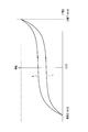
- FIG. 3 is a diagram showing the relationship between the input voltage of the reflective liquid crystal display element using ferroelectric liquid crystal and the intensity of output light.
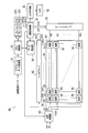
- FIG. 4 is a block diagram of the first embodiment of the liquid crystal display device of the present invention.
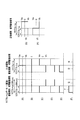
- 5 (A) to 5 (H) are signal explanatory diagrams of the respective parts in FIG. 2 and
- FIGS. 6A to 6C are explanatory diagrams showing examples of drive patterns in the first embodiment of the liquid crystal display device of the present invention.
- FIG. 1 is a schematic configuration diagram of an example of a projection display device using a reflective liquid crystal display element to which the present invention is applied.
- FIG. 2 is a configuration diagram of one pixel of the first embodiment of the digitally driven reflective liquid crystal display element in
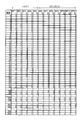
- FIG. 7 is a diagram showing an example of a gradation table used in the subframe data conversion unit in the liquid crystal display device of the present invention.
- FIGS. 8A to 8M are timing charts for explaining the operation of FIGS.
- FIG. 9 is a block diagram of one pixel of the second embodiment of the digitally driven reflective liquid crystal display element in FIG.
- FIG. 10 is a block diagram of a second embodiment of the liquid crystal display device of the present invention.
- 11 (A) to 11 (H) are signal explanatory diagrams of the respective parts in FIGS. 9 and 10.
- FIG. FIGS. 12A to 12C are explanatory diagrams of examples of drive patterns in the second embodiment of the liquid crystal display device of the present invention.
- FIGS. 13A to 13M are timing charts for explaining the operation of FIGS.
- the present invention can be applied to a panel type liquid crystal display device including a display panel in which a plurality of pixels each including a ferroelectric liquid crystal are arranged in a matrix.
- a panel type liquid crystal display device including a display panel in which a plurality of pixels each including a ferroelectric liquid crystal are arranged in a matrix.
- an active matrix type is used as a display panel.
- An explanation will be given by taking as an example a projection display device provided with a reflective liquid crystal display element. First, a schematic configuration of a projection display device and a reflective liquid crystal display element to which the present invention is applied will be described.
- FIG. 1 shows a schematic configuration diagram of an example of a projection display device using a reflective liquid crystal display element to which the present invention is applied.
- the projection display device 10 includes a reflective liquid crystal display element 11, a polarization beam splitter (hereinafter referred to as PBS) 16, and a projection lens 17. The light irradiated from the projection lens 17 is projected onto the screen 18.
- PBS polarization beam splitter
- the reflective liquid crystal display element 11 includes a plurality of pixel electrodes 12 having conductivity and light reflectivity, a liquid crystal layer 13 made of ferroelectric liquid crystal, and a common conductivity and light transmittance common to the plurality of pixel electrodes 12.
- An electrode (transparent electrode) 14 and a pixel circuit 15 are included.
- the plurality of pixel electrodes 12 are arranged in a two-dimensional matrix on the surface of a first substrate (not shown).
- FIG. 1 shows only one arbitrary pixel electrode among the plurality of pixel electrodes 12.
- the common electrode 14 is formed on the surface of a second substrate (not shown).
- the liquid crystal layer 13 is made of ferroelectric liquid crystal, and sealed in a space between the substrates formed by separating the first substrate and the second substrate so that the pixel electrode 12 and the common electrode 14 face each other. Has been. Each surface of the pixel electrode 12 and the common electrode 14 is covered with an alignment film (not shown).
- the pixel circuit 15 is provided on the first substrate together with a drive circuit including a drive control unit 34 and the like, which will be described later, which constitute a main part of the present invention, and is electrically connected to the pixel electrode 12.
- incident light L1 that is a backlight emitted from an illumination optical system (not shown) enters the PBS 16.
- the incident light L1 includes an S-polarized component and a P-polarized component whose planes of polarization are orthogonal to each other.
- the P-polarized light component is schematically indicated by a line segment (P)
- the S-polarized light component is indicated by a circle (S).
- the PBS 16 has an optical characteristic of reflecting the S-polarized component of incident light and transmitting the P-polarized component. Accordingly, the PBS 16 reflects the S-polarized component of the incident light L 1 and enters the common electrode 14.
- the S-polarized component incident on the common electrode 14 is incident on the pixel electrode 12 through the liquid crystal layer 13 to be reflected, and the reflected light from the pixel electrode 12 is emitted through the liquid crystal layer 13 and the common electrode 14.
- the S-polarized component incident on the common electrode 14 is modulated according to the potential difference between the drive voltage according to the common voltage applied to the common electrode 14, and a part of the S-polarized component is used as the P-polarized component.
- the light is emitted as an S-polarized component and a P-polarized component.
- the PBS 16 transmits the P-polarized component of the light emitted from the reflective liquid crystal display element 11 and enters the projection lens 17, and the S-polarized component reflects and enters the illumination optical system.
- the projection lens 17 projects the P-polarized component from the PBS 16 onto the screen 18 as outgoing light L2, and displays an image.
- the “output light intensity” described later refers to the illuminance of the emitted light L2 measured on the screen 18.
- FIG. 2 shows a configuration diagram of one pixel of the first embodiment of the liquid crystal display device according to the present invention.
- one pixel 20 of the reflective liquid crystal display element 11 in the first embodiment of the liquid crystal display device of the present invention includes a pixel circuit 15a and a liquid crystal element LC, and includes a column data line D and a row selection line. It is arranged at the intersection with W.
- the liquid crystal element LC is a ferroelectric liquid crystal in the space between the substrates formed by separating the first substrate and the second substrate so that the pixel electrode 12 and the common electrode 14 face each other. The layer 13 is enclosed.
- the pixel circuit 15 a is a first embodiment of the pixel circuit 15 of FIG. 1 and includes a sub-sample hold unit 21, a transfer switching transistor 22, a main sample hold unit 23, and a voltage selection unit 24.
- the sub-sample hold unit 21 and the main sample hold unit 23 are composed of SRAM (Static Random Access Memory) structure flip-flops.
- the subsample hold unit 21 is connected to the column data line D and the row selection line W. When selected by a row selection signal applied via the row selection line W, the subsample hold unit 21 passes through the column data line D. The supplied pixel data is sampled and held.
- the transfer switching transistor 22 has a source connected to the output terminal of the sub-sample hold unit 21, a drain connected to the input terminal of the main sample hold unit 23, and a gate connected to the transfer signal line T. Activated when a transfer signal having a predetermined logic value is applied via the signal line T, and transfers the subframe data (pixel data voltage) held in the subsample hold unit 21 to the main sample hold unit 23. To do.
- the main sample hold unit 23 samples and holds the subframe data (pixel data voltage) input through the transfer switching transistor 22.
- the voltage selection unit 24 is connected to the blanking voltage line V0 and the drive voltage line V1. An output terminal of the voltage selection unit 24 is connected to the pixel electrode 12.
- the voltage selection unit 24 determines whether the blanking voltage line V0 is blanked according to whether the value of the subframe data (pixel data voltage) held by the main sample hold unit 23 is “0” or “1”.
- One of the voltage and the driving voltage of the driving voltage line V ⁇ b> 1 is selected and applied to the pixel electrode 12.
- the voltage applied to the common electrode 14 is called a common voltage Vcom.
- FIG. 3 is a diagram showing the relationship between the input voltage of the reflective liquid crystal display element 11 using ferroelectric liquid crystal and the intensity of output light in each embodiment.
- the horizontal axis represents the input voltage, and shows the potential difference between the pixel electrode 12 and the common electrode 14, that is, the driving voltage of the liquid crystal layer 13.
- the vertical axis in FIG. 3 indicates the intensity (luminance) of output light emitted from the liquid crystal layer 13.
- the liquid crystal layer 13 performs black display with the minimum luminance when the voltage Vb [V] is applied, and performs white display with the maximum luminance when the voltage Vw [V] is applied (in the following description, the voltage Vb is the black voltage and the voltage Vw is the voltage Vb [V]). Also called white voltage).
- the ferroelectric liquid crystal that constitutes the liquid crystal layer 13 changes the intensity of the output light as shown by the curve I when the input voltage gradually increases from the black voltage Vb [V] to the white voltage Vw [V].
- the output light intensity changes as shown by the curve II.
- the ferroelectric liquid crystal constituting the liquid crystal layer 13 has hysteresis characteristics as shown in FIG. For this reason, when the input voltage is 0 [V] in the middle between the black voltage Vb [V] and the white voltage Vw [V], the luminance changes depending on the voltage immediately before.
- the black voltage Vb [V] or the white voltage Vw [V] is applied to the liquid crystal display element as will be described later.
- the black voltage Vb [V] is a negative voltage
- the white voltage Vw [V] is a positive voltage.
- FIG. 4 shows a block diagram of the first embodiment of the liquid crystal display device of the present invention.
- the liquid crystal display device 30 includes a subframe data conversion unit 31, a memory control unit 32, a frame buffer A331 and a frame buffer B332, a drive control unit 34, an LED control unit 35, a data transfer unit 36, a source driver 37, A voltage control unit 38, a gate driver 39, and a pixel unit 40 are included.
- the pixel section 40 is composed of (n + 1) ⁇ (m + 1) pixels 20 arranged at each intersection where n + 1 column data lines D0 to Dn and m + 1 row selection lines W0 to Wm intersect. Is done.
- One pixel 20 has the configuration shown in FIG. Further, in all the pixels 20 of the pixel unit 40, the blanking voltage line V0 and the drive voltage line V1 are commonly connected to each voltage selection unit 24, and the transfer signal line T is common to the gate of each transfer switching transistor 22. It is connected to the.
- the LED control unit 35 drives and controls the light emitting diode (LED) 42 constituting the illumination optical system described above to be turned on or off. Further, the LED control unit 35 has an LED weighting table, and has a function of predetermining the light emission period of the LED 35 for each subframe based on the LED weighting table, as will be described later.
- LED light emitting diode
- the memory control unit 32 supplies, for example, subframe data of 12 bits per frame supplied from the subframe data conversion unit 31 to the two frame buffers A331 and B332. Then, the memory control unit 32 alternately writes subframe data to one frame buffer and simultaneously reads subframe data stored from the other frame buffer in units of one frame period. That is, the frame buffer A331 and the frame buffer B332 have a double buffer structure (that is, a structure having two sets of frame buffers divided into 12 subframes).
- the period in which the frame buffer A331 is writing the 12 subframe data of one frame supplied through the memory control unit 32 is the 12 subframes of 1 frame immediately before being written from the frame buffer B332. Data is read by the memory control unit 32.
- the frame buffer B332 writes 12 subframe data, and in parallel, the frame buffer A331 reads 12 subframe data of the immediately preceding frame. Thereafter, the above operation is repeated.
- the drive control unit 34 is supplied with the vertical synchronization signal VSYNC and the horizontal synchronization signal HSYNC of the video signal data supplied to the sub-frame data conversion unit 31, and the drive control unit 34 synchronizes these signals with the data transfer timing.
- the voltage control timing, the LED control timing, and the like are controlled, the transfer instruction to the data transfer unit 36, the control of the source driver 37 / gate driver 39, and the timing instruction to the voltage control unit 38 and the LED control unit 35 are performed.
- the data transfer unit 36 instructs the memory control unit 32 according to the instruction from the drive control unit 34, and the designated subframe data among the subframe data read from the frame buffer A331 or the frame buffer B332 by the memory control unit 32 is transmitted. Receive and transfer to source driver 37.
- the source driver 37 shifts the subframe data from the data transfer unit 36 according to the horizontal start signal (HST) / horizontal shift clock signal (HCK) from the drive control unit 34. Each time the source driver 37 receives sub-frame data of (n + 1) pixels for one line, the source driver 37 simultaneously transfers the sub-frame data for one line to the pixel unit 40 via the column data lines D0 to Dn in parallel. To do.
- HST horizontal start signal
- HK horizontal shift clock signal
- the gate driver 39 sequentially supplies a row selection signal to the row selection lines W0 to Wm every one horizontal scanning period in response to a vertical start signal (VST) / vertical shift clock signal (VCK) from the drive control unit 34.
- the plurality of pixels 20 in the section 40 are sequentially selected in line units from top to bottom. For example, when the gate driver 39 activates the row selection line Wy of the designated one line (row) y among the row selection lines W0 to Wm, the (n + 1) pixels 20 of the designated row y are selected.
- the sub-frame data of (n + 1) pixels for one line input in parallel from the source driver 37 via the column data lines D0 to Dn to each sub-sample hold unit 21 in each selected pixel 20 is a pixel. It is transferred and held separately.
- the source driver 37 and the gate driver 39 constitute the pixel unit driving means of the present invention.
- the drive control unit 34 The transfer switching transistors 22 in all the pixels 20 are activated by the transfer signal on the transfer signal line T from the sub-frame data, and the sub-frame data held in the sub-sample hold unit 21 is transferred to the main sample hold unit 23. Transferred, sampled and held.
- the subframe data which is pixel data sampled and held in the main sample hold unit 23 and applied to the voltage selection unit 24, has a value of “1” or “0” depending on the gradation to be displayed in the pixel. have.
- the voltage control unit 38 in FIG. 4 supplies a blanking voltage to all the pixels 20 of the pixel unit 40 via the blanking voltage line V0 according to the instruction of the drive control unit 34, and supplies the drive voltage line V1 to the pixel 20.
- a drive voltage is supplied via
- the blanking voltage and the driving voltage are symmetrical square waves each having one subframe period of a subframe as one cycle, and are in opposite phases (reverse polarity). That is, when one subframe period is divided into a first half period and a second half period, the first half period is a drive period, and the second half period is a compensation drive period, the blanking voltage of the blanking voltage line V0 is as shown in FIG.
- the black voltage Vb [V] is used in the driving period
- the white voltage Vw [V] is used in the compensation driving period.
- the drive voltage of the drive voltage line V1 is the white voltage Vw [V] in the drive period and the black voltage Vb [V] in the compensation drive period.
- the voltage selection unit 24 of FIG. 2 is shown in FIG. 5 (H) as shown in FIG.
- the drive voltage of the drive voltage line V1 is selected and applied to the pixel electrode 12
- the value of the subframe data is “0”, as shown in FIG. 5A
- the drive voltage line V1 is shown in FIG.
- the blanking voltage of the blanking voltage line V0 is selected and applied to the pixel electrode 12.
- a common voltage Vcom having a constant voltage of 0 [V] shown in FIG.
- This constant voltage 0 [V] is an intermediate voltage between the black voltage Vb [V] and the white voltage Vw [V].
- the drive voltage applied to the liquid crystal layer 13 has a value of subframe data as shown in FIG.
- the value is “1”
- the white voltage Vw [V] is used during the driving period
- the black voltage Vb [V] is used during the compensation driving period
- the black voltage Vb [V] is displayed during the driving period.
- V] and the white voltage Vw [V] in the compensation drive period when the value is “1”, the white voltage Vw [V] is used during the driving period, the black voltage Vb [V] is used during the compensation driving period, and when the value of the subframe data is “0”, the black voltage Vb [V] is displayed during the driving period. V] and the white voltage Vw [V] in the compensation drive period.
- the drive waveform of the liquid crystal element LC is schematically shown at a high level in FIG.
- the value of the subframe data is “1”, it is driven in the driving period, and when the value of the subframe data is “0”, it is driven in the compensation driving period. That is, in the liquid crystal display device 30 of the present embodiment, as described later, when the gradation of the pixel is “0” and the values of the 12 subframe data are all “0”, the liquid crystal display device 30 is not driven in the driving period. Since driving is performed in the compensation driving period, AC driving can always be ensured, and as a result, sufficient burn-in prevention can be performed.
- the LED control unit 35 drives the LED 42 according to the instruction from the drive control unit 34 as schematically shown at a high level in FIG. 5E only within the drive period regardless of the value of the subframe data.
- the illumination light is emitted, and the illumination light is emitted from the LED 42 in the illumination optical system as the incident light L 1 shown in FIG. 1 and enters the liquid crystal display element 11.
- the LED control unit 35 drives the LED 42 in the drive period.
- the LED weighting table which number of subframe periods among the 12 subframe periods that constitute one frame period is. Accordingly, the LED 42 is caused to emit light in a predetermined setting period equal to or shorter than the entire driving period (694 ⁇ s).
- the liquid crystal element LC constituting a part of the liquid crystal driving element 11 is driven in a driving period in which incident light is incident when the value of the subframe data is “1”. Therefore, as schematically shown at the high level f1 in FIG. 5 (F), the emitted light L2 shown in FIG. 1 is output to perform white display.
- the liquid crystal element LC when the value of the subframe data is “0” in the driving period, the liquid crystal element LC is not driven even when incident light is incident. As schematically shown by the level f3, the emitted light L2 is not output and black display is performed.
- the liquid crystal element LC When the value of the subframe data is “0”, the liquid crystal element LC is driven as schematically shown at a high level in FIG. 5D during the compensation driving period, but is low in FIG. 5E. Since illumination light does not enter the liquid crystal element LC as schematically shown by the level, the emitted light L2 is not output and black display is performed as schematically shown by the low level f4 in FIG.
- FIGS. 6A to 6C are explanatory diagrams showing examples of drive patterns in the first embodiment of the liquid crystal display device according to the present invention.
- FIGS. 6A to 6C show driving patterns of the liquid crystal display device 30 of the present embodiment when the video signal is 60 frames per second and the number of subframes is 12. Yes.
- One subframe period is 1389 [ ⁇ s]. That is, FIG. 6A shows that a total of 12 subframes from the second subframe SF2 to the first subframe SF1 are transferred in one frame period.
- FIG. 6B shows that, as described above, each subframe period is set to the driving period in the first half period and the compensation driving period in the second half period.
- FIG. 6C shows that the LED 42 as the light source is set by the LED control unit 35 to emit light in the second half of the driving period in the subframes SF1 to SF6. That is, the LED control unit 35 increases the weight of the light emission period of the LED 42 in the drive period from the subframe SF1 to SF12, and starts from the end of the drive period in the order of the subframes SF1, SF2, SF3, SF4, and SF5.
- the LED 42 is controlled so as to be longer in the start end direction and to have the entire drive period as the light emission period in the subframes SF6 to SF12 having the maximum weight. By emitting light in the second half of the driving period, it is possible to reduce the loss during the rising period of the liquid crystal layer 13.
- the LED 42 emits light in the same period as the drive period in the subframes SF6 to SF12, and in the subframes SF1, SF2, SF3, SF4, and SF5, It shows that light is emitted for periods of 1/32 times, 2/32 times, 4/32 times, 8/32 times, and 16/32 times.
- the LED control section 35 refers to the LED weighting table for the operation of weighting and variably controlling the LED light emission period according to the number of subframes SF1 to SF12 in one frame period. Do.
- FIG. 7 shows an example of the gradation table.
- the gradation table is a table that the subframe data conversion unit 31 refers to according to the pixel value (gradation value) of the video signal data when the video signal data is converted into subframe data and output.
- the vertical axis indicates the gradation value
- the horizontal axis indicates the subframes SF1 to SF12, thereby determining the value of each subframe data corresponding to the gradation value.
- the gradation table shown in FIG. 7 expresses gradations 0 to 255 by performing “binary” weighting for subframes SF1 to SF5 and “step bit” for subframes SF6 to SF12. To do.
- a total of 32 levels of brightness (gradation) from 0 to 31 levels can be expressed using five binary bit pulses, and a large number of gradations can be expressed even with a small number of pulses. Accordingly, in FIG.
- the value of each subframe data of SF12 is “0”).
- gradation “127” represents gradation “31” with the value of each subframe data of SF1 to SF5 being “1”, and in addition to this, among SF6 to SF12 for weighting step bits, SF6 to SF12
- the subframe SF1 is subframed according to the instruction of the drive control unit 34 as shown in FIG. 8B.
- Frame data is sequentially input from the data transfer unit 36 to the source driver 37.
- the source driver 37 simultaneously transfers the column data lines D0 to Dn to the pixel unit 40 via the parallel lines, and designates the row (1) specified by the gate driver 39.
- Each sub-sample hold unit 21 in each of the (n + 1) pixels 20 of the line y is sampled and held for each pixel.
- the main sample hold unit 23 holds SF1 subframe data “1” at time T1. . As shown in FIG. 8E, the main sample hold unit 23 holds the SF1 subframe data “1” during the period (T1-T3) during which the next SF2 subframe data is transferred. Is done.
- the voltage selection unit 24 of the pixel 20 has a black voltage as shown in FIG. 8F through the blanking voltage line V0 in the driving period which is the first half period of one subframe period.
- Vb [V] is applied as a blanking voltage
- a white voltage Vw [V] as shown in FIG. 8G is applied through the drive voltage line V1. Therefore, the voltage selection unit 24 uses the voltage V1 based on the subframe data “1” held in the main sample hold unit 23 in the driving period (T1-T2) which is the first half period of one subframe period (T1-T3).
- white voltage Vw [V] is applied to the pixel electrode 12 as schematically shown at a high level in FIG.
- the LED control unit 35 lights the LED 42 during the SF1 drive period (T1-T2) only during a weighting period 1/32 times the drive period as schematically shown at a high level in FIG. . Therefore, in the driving period (T1-T2) of SF1, the pixel 20 (x, y) of the liquid crystal display device 30 is white during the above weighting period as schematically shown at a high level in FIG. Display.
- the voltage selection unit 24 sets the subframe data “1” held in the main sample hold unit 23 in the compensation driving period (T2-T3), which is the latter half of one subframe period (T1-T3). Based on this, the voltage V0 is selected, and the black voltage Vb [V] is applied to the pixel electrode 12 as shown by the low level in FIG. At this time, since the common voltage Vcom of 0 [V] shown in FIG. 8H is applied to the common electrode 14 of the liquid crystal element LC, the driving voltage shown in FIG. Is applied, and the liquid crystal element LC is driven with a voltage having a polarity opposite to that of the driving period in the compensation driving period (T2-T3) as schematically shown at a low level in FIG.
- the LED control unit 35 does not drive the LED 42 in the compensation drive period (T2-T3) of SF1, as shown in FIG. Therefore, in the compensation driving period (T2-T3) of SF1, the pixel 20 (x, y) of the liquid crystal display device 30 performs black display as schematically shown at a low level in FIG.
- the sub-frame data “0” of SF2 is held in the main sample hold unit 23 at time T3.
- the SF2 subframe data “0” is held during a period (T3-T5) during which the next SF3 subframe data is transferred, as shown in FIG. Is done.
- the voltage selection unit 24 determines the voltage based on the subframe data “0” held in the main sample hold unit 23 in the driving period (T3-T4) which is the first half period of one subframe period (T3-T5).
- V0 is selected, and a black voltage Vb [V] is applied to the pixel electrode 12 as shown by a low level in FIG.
- the common voltage Vcom of 0 [V] shown in FIG. 8H is applied to the common electrode 14 of the liquid crystal element LC, the driving voltage shown in FIG. Is applied, and the liquid crystal element LC is driven at a voltage corresponding to the black voltage Vb [V] in the driving period (T3-T4) as schematically shown at a low level in FIG.
- the LED control unit 35 lights the LED 42 during the SF2 drive period (T3-T4) as shown in FIG. 8L for a weighting period that is 2/32 times the drive period. Therefore, in the driving period (T3-T4) of SF2, the pixel 20 (x, y) of the liquid crystal display device 30 is black during the above-described weighting period as schematically shown at low level in FIG. Display.
- the voltage selection unit 24 sets the subframe data “0” held in the main sample hold unit 23 in the compensation driving period (T4-T5) which is the latter half of one subframe period (T3-T5). Based on this, the voltage V1 is selected, and the white voltage Vw [V] is applied to the pixel electrode 12 as shown at a high level in FIG. At this time, since the common voltage Vcom of 0 [V] shown in FIG. 8H is applied to the common electrode 14 of the liquid crystal element LC, the driving voltage shown in FIG. Is applied, and the liquid crystal element LC is driven with a white voltage in the compensation driving period (T4-T5) as schematically shown at a high level in FIG.
- the LED control unit 35 does not drive the LED 42 as shown in FIG. 8 (L) in the compensation driving period (T4-T5) of SF2. Accordingly, since there is no illumination light in the compensation driving period (T4-T5) of SF2, the pixel 20 (x, y) of the liquid crystal display device 30 has a light output of 0 and is schematically shown at a low level in FIG. Display black as shown.
- the driving is performed even when the gradation of the pixel is “0” and the values of the 12 subframe data of SF1 to SF12 are all “0”.
- voltages having opposite polarities black voltage and white voltage
- AC driving can always be secured, and as a result, sufficient burn-in prevention is performed. be able to.
- one frame period is divided into 12 subframe periods, and the liquid crystal element LC is AC driven every subframe period, so 12 times per frame. More DC balance polarity reversal than before can be performed, and the burn-in prevention accuracy can be improved. As a result, the reliability of the liquid crystal display device using the ferroelectric liquid crystal can be improved.
- liquid crystal display device 30 of the present embodiment voltages (black voltage and white voltage) having opposite polarities are applied to the pixel electrode 12 in the first half drive period and the second half compensation drive period of one subframe.
- voltages black voltage and white voltage
- the driving method of the liquid crystal display device described in Patent Document 3 can be eliminated.
- FIG. 9 shows a configuration diagram of one pixel of the second embodiment of the liquid crystal display device according to the present invention. 9, the same components as those in FIGS. 1 and 2 are denoted by the same reference numerals.
- One pixel 50 of the reflective liquid crystal display element 11 in the second embodiment of the liquid crystal display device of the present invention is composed of a pixel circuit 15b and a liquid crystal element LC, and two column data lines D and inverted column data lines. The data line and the row selection line W are arranged at the intersection of DX as a set.
- the liquid crystal element LC has a ferroelectric property in the space between the substrates formed by separating the first substrate and the second substrate so that the pixel electrode 12 and the common electrode 14 face each other.
- the liquid crystal layer 13 is enclosed. 2 and 9, the liquid crystal elements LC are illustrated in units of pixel circuits in order to facilitate understanding that the liquid crystal elements LC are provided in units of pixel circuits 15a and 15b.
- the pixel electrode 12 is individually provided for each of the pixel circuits 15a and 15b, but the liquid crystal layer 13 and the common electrode 14 are provided in common for all the pixels.
- the pixel circuit 15b is a second embodiment of the pixel circuit 15 of FIG. 1, and includes a sample hold unit 51 and a voltage selection unit 52 as shown in FIG.
- the sample hold unit 51 is composed of a flip-flop having an SRAM (Static Random Access Memory) structure.
- the sample hold unit 51 is connected to the column data line D, the inverted column data line DX, and the row selection line W, and when selected by a row selection signal applied via the row selection line W, The pixel data supplied via the data line D and the inverted column data line DX is sampled and held.
- the voltage selection unit 52 is connected to the sample hold unit 51, the blanking voltage line V0, and the drive voltage line V1.
- the output terminal of the voltage selection unit 52 is connected to the pixel electrode 12.
- the voltage selection unit 24 determines whether the blanking voltage line V0 is blanked according to whether the value of the subframe data (pixel data voltage) held by the sample hold unit 51 is “0” or “1”. One of the voltage and the driving voltage of the driving voltage line V ⁇ b> 1 is selected and applied to the pixel electrode 12.
- FIG. 10 shows a block diagram of a second embodiment of the liquid crystal display device of the present invention.
- the liquid crystal display device 60 of the present embodiment includes a subframe data conversion unit 31, a memory control unit 32, a frame buffer A331 and a frame buffer B332, an LED control unit 35, a data transfer unit 36, a gate driver 39, a drive control unit 61, A source driver 62, a voltage control unit 63, and a pixel unit 64 are included.
- the pixel unit 64 includes (n + 1) sets of column data lines D0 to Dn and inverted column data lines DX0 to DXn, each of which includes one column data line D and one inverted column data line DX, and m + 1 It is composed of (n + 1) ⁇ (m + 1) pixels 50 arranged at each intersection where the row selection lines W0 to Wm intersect.
- One pixel 50 has the configuration shown in FIG. Further, in all the pixels 50 of the pixel unit 64, the blanking voltage line V 0 and the drive voltage line V 1 are commonly connected to each voltage selection unit 52.
- the drive control unit 61 is supplied with the vertical synchronization signal VSYNC and the horizontal synchronization signal HSYNC of the video signal data supplied to the sub-frame data conversion unit 31, and the drive control unit 61 synchronizes these signals with the data transfer timing.
- the voltage control timing, the LED control timing, and the like are controlled, the transfer instruction to the data transfer unit 36, the control of the source driver 62 / gate driver 39, and the timing instruction to the voltage control unit 63 and the LED control unit 35 are performed.
- the data transfer unit 36 instructs the memory control unit 32 according to the instruction from the drive control unit 61, and the designated subframe data among the subframe data read from the frame buffer A331 or the frame buffer B332 by the memory control unit 32 is transmitted. Receive and transfer to source driver 62.
- the source driver 62 shifts the subframe data from the data transfer unit 36 according to the horizontal start signal (HST) / horizontal shift clock signal (HCK) from the drive control unit 61. Each time the source driver 62 receives sub-frame data of (n + 1) pixels for one line, the source driver 62 converts two types of sub-frame data of opposite logical values for the one line into column data lines D0 to Dn and inverted columns. Data lines DX0 to DXn are simultaneously transferred to the pixel portion 64 via the parallel lines.
- the value of the inverted subframe data transferred by the inverted column data line DXi is in an inverse logical value relationship such that when one is always “1”, the other is “0”.
- the use of the column data lines D0 to Dn and the inverted column data lines DX0 to DXn in the present embodiment corresponds to the use of the SRAM by the flip-flop circuit as the sample hold unit 51 in the pixel 50. This is because the configuration is more realistic.
- the SRAM requires two data having opposite logical values in order to stably hold the data.
- only one type of column data line is required as in the liquid crystal display device 30 of the first embodiment of FIG.
- the gate driver 39 sequentially supplies a row selection signal to the row selection lines W0 to Wm every one horizontal scanning period in response to a vertical start signal (VST) / vertical shift clock signal (VCK) from the drive control unit 61.
- the plurality of pixels 50 of the unit 64 are sequentially selected in line units from the top to the bottom. For example, when the gate driver 39 activates the row selection line Wy of the designated one line (row) y among the row selection lines W0 to Wm, the (n + 1) pixels 50 of the designated row y are selected. (N + 1) for one line inputted in parallel from the source driver 62 via the column data lines D0 to Dn and the inverted column data lines DX0 to DXn to each sample and hold unit 51 in each selected pixel 50. Pixel sub-frame data is transferred and held for each pixel.
- the source driver 62 and the gate driver 39 constitute the pixel unit driving means of the present invention.
- the above operation is repeated in units of one line, and all the subframe data in one subframe period are transferred to the sample hold unit 51 in all the pixels 50 of the pixel unit 64 within a compensation driving period to be described later for sampling and sampling. Is held.
- the subframe data that is pixel data has a value of “1” or “0” depending on the gradation to be displayed by the pixel.
- the voltage control unit 63 in FIG. 10 supplies a blanking voltage to all the pixels 50 of the pixel unit 64 through the blanking voltage line V0 according to an instruction from the drive control unit 61, and also supplies the driving voltage line V1 to the pixel 50.
- a drive voltage is supplied via
- the blanking voltage and the driving voltage are symmetrical square waves each having one subframe period of a subframe as one cycle, and are in opposite phases (reverse polarity). That is, when one subframe period is divided into a first half period and a second half period, the first half period is a compensation drive period, and the second half period is a drive period, the blanking voltage of the blanking voltage line V0 is as shown in FIG.
- the white voltage Vw [V] is used in the compensation driving period
- the black voltage Vb [V] is used in the driving period.
- the drive voltage of the drive voltage line V1 is the black voltage Vb [V] in the compensation drive period and the white voltage Vw [V] in the drive period.
- the voltage selection unit 52 in FIG. When the value of the subframe data input via the column data line D held by the sample hold unit 51 is “1” (that is, via the inverted column data line DX), the voltage selection unit 52 in FIG. When the value of the input inverted subframe data is “0”), as shown in FIG. 11A, the drive voltage of the drive voltage line V1 shown in FIG. Apply to. On the other hand, when the value of the subframe data input via the column data line D is “0” (that is, the value of the inverted subframe data input via the inverted column data line DX is When “1”, as shown in FIG. 11A, the blanking voltage of the blanking voltage line V 0 shown in FIG. 11G is selected and applied to the pixel electrode 12.
- a common voltage Vcom having a constant voltage 0 [V] shown in FIG. 11B is applied from the voltage control unit 63 to the common electrode 14 of the liquid crystal element LC.
- This constant voltage 0 [V] is an intermediate voltage between the black voltage Vb [V] and the white voltage Vw [V]. Since the liquid crystal layer 13 is driven by a potential difference between the applied voltage of the pixel electrode 12 and the common voltage Vcom, the drive voltage applied to the liquid crystal layer 13 has a value of subframe data as shown in FIG.
- the value is “1” (the value of the inverted subframe data is “0”)
- the black voltage Vb [V] is set in the compensation driving period
- the white voltage Vw [V] is set in the driving period
- the subframe data value is “0”. "(The value of the inverted subframe data is” 1 ")
- the white voltage Vw [V] is used in the compensation driving period and the black voltage Vb [V] is used in the driving period.
- the drive waveform of the liquid crystal element LC is schematically shown at a high level in FIG.
- the subframe data is driven in the driving period
- the value of the subframe data is “0” (the value of the inverted subframe data is In the case of “1”)
- the driving is performed in the compensation driving period. That is, in the liquid crystal display device 60 of the present embodiment, as described later, when the pixel gradation is “0” and the values of the twelve subframe data are all “0”, the liquid crystal display device 60 is not driven in the driving period. Since driving is performed in the compensation driving period, AC driving can always be ensured, and as a result, sufficient burn-in prevention can be performed.
- the LED control unit 35 drives the LED 42 according to an instruction from the drive control unit 61 as schematically shown at a high level in FIG. 11E only within the drive period regardless of the value of the subframe data.
- the illumination light is emitted, and the illumination light is emitted from the LED 42 in the illumination optical system as the incident light L 1 shown in FIG. 1 and enters the liquid crystal display element 11.
- the LED control unit 35 drives the LED 42 in the drive period.
- the LED weighting table which number of subframe periods among the 12 subframe periods that constitute one frame period is. Accordingly, the LED 42 is caused to emit light in a predetermined setting period that is equal to or less than the entire driving period.
- the liquid crystal element LC constituting a part of the liquid crystal driving element 11 has a subframe data value “1” (inverted subframe data value “0”).
- the emitted light L2 shown in FIG. 1 is output and white display is performed as schematically shown at the high level f14 in FIG.
- the liquid crystal element LC is schematically shown at a high level in FIG. 11D during the compensation drive period. Although driven, illumination light does not enter the liquid crystal element LC as schematically shown at low level in FIG. 11 (E), so that the emitted light L2 is schematically shown at low level f11 in FIG. 11 (F). Is not output and black is displayed.
- FIG. 12 is an explanatory diagram showing an example of a drive pattern in the liquid crystal display device according to the second embodiment of the present invention. Specifically, FIG. 12 shows a driving pattern of the liquid crystal display device 60 of the present embodiment when the number of subframes is twelve. FIG. 12A shows that a total of 12 subframe transfers from the subframe SF1 to the subframe SF12 are performed in one frame period. When the period for rewriting the information (subframe data) of the sample hold unit 51 in all the pixels 50 is a data address period, the data address period ends within the compensation driving period which is the first half period in each subframe. There is a need.
- FIG. 12B shows that each subframe period is set as a compensation driving period and the latter half period is set as a compensation driving period as described above. That is, the compensation driving period is performed during the data address period.
- FIG. 12C shows that the LED 42 as the light source is set by the LED control unit 35 to emit light in the second half of the driving period in SF1 to SF6. That is, the LED control unit 35 increases the weight of the light emission period of the LED 42 in the drive period from the subframe SF1 to SF12, and starts from the end of the drive period in the order of the subframes SF1, SF2, SF3, SF4, and SF5.
- the LED 42 is controlled so as to be longer in the start end direction and to have the entire drive period as the light emission period in the subframes SF6 to SF12 having the maximum weight. By emitting light in the second half of the driving period, it is possible to reduce the loss during the rising period of the liquid crystal layer 13.
- the period from the end of the driving period of the last sub-frame SF12 to the start of the next frame is set as the “non-driving period” so that the voltage applied to the liquid crystal layer 13 becomes 0 [V]. That is, the blanking voltage of the blanking voltage line V0 and the driving voltage of the driving voltage line V1 are set to have the same voltage value as the common electrode voltage Vcom. This is because it is very difficult to make the total period of the subframes coincide with the frame period. Therefore, an extra period is inevitably generated, and if an extra voltage is applied to the liquid crystal element LC during the extra period, it causes burn-in. This is to prevent this.
- the extra period is a non-driving period in which the blanking voltage of the blanking voltage line V0, the driving voltage of the driving voltage line V1, and the common electrode voltage Vcom are set to the same voltage value and the liquid crystal element LC is not driven.
- the voltage applied to the liquid crystal element LC can be set to 0 and burn-in can be prevented regardless of the value of the subframe data held by the sample hold unit 51.
- the LED 42 emits light in the same period as the drive period in the subframes SF6 to SF12, and in the subframes SF1, SF2, SF3, SF4, and SF5, It shows that light is emitted for periods of 1/32 times, 2/32 times, 4/32 times, 8/32 times, and 16/32 times.
- the LED control unit performs the variable control by weighting the light emission period of the LED in accordance with the number of the subframes SF1 to SF12 within one frame period, as in the first embodiment. 35 with reference to the LED weighting table.
- the subframe SF1 is subframed according to the instruction of the drive control unit 61 as shown in FIG.
- Frame data is sequentially input from the data transfer unit 36 to the source driver 62.
- the source driver 37 stores (n + 1) subframe data for one line
- the subframe data and the inverted subframe data are simultaneously transmitted via the column data lines D0 to Dn and the inverted column data DX0 to DXn in parallel.
- the data is transferred to the pixel unit 64, and is sampled and held for each pixel by each sample hold unit 51 in each of the (n + 1) pixels 50 in the row (one line) y designated by the gate driver 39.
- each 1-bit value of 12 subframe data D (x, y) from SF1 to SF12 input in one pixel 50 (x, y) in the pixel unit 50 is shown in FIG. [1, 0, 1, 1, 0, 1, 1, 1, 1, 0, 0, 0] as shown in FIG.
- the description of the inverted subframe data is omitted.
- the transmission period of the first subframe SF1 as shown in FIG. 13C, at the time T11 delayed by y lines from the input time T0 of the vertical synchronization signal VSYNC, Each pixel 50 in the y-th line is selected by the supplied row selection signal Wy, and the subframe data “1” of the subframe SF1 is held in the sample hold unit 51 in each pixel 50.
- the subframe data “1” of SF1 in the sample hold unit 51 in the pixel 50 (x, y) is held at time T16 when the next subframe data of SF2 is transferred as shown in FIG. Up to (T11-T16).
- one subframe of subframe SF1 is a period (T0-T15) from time T0 to time T15 shown in FIG. 13B, and is from the time T0 to time T13 which is the first half period of the one subframe.
- the white voltage Vw [V] shown at high level in FIG. 13 (F) is applied to the blanking voltage line V0 as the compensation drive period, and the drive voltage line V1 is applied to FIG. 13 (G).
- a black voltage Vb [V] indicated by a low level is applied.
- T13-T15 which is the latter half period of one subframe of SF1
- the black voltage Vb shown as a low level in FIG. [V] is applied to the drive voltage line V1
- the white voltage Vw [V] shown at a high level in FIG. 13G is applied.
- the common electrode voltage Vcom is always 0 [V] as shown in FIG.
- the subframe data value held by the sample hold unit 51 in the pixel 50 (x, y) is “1” as shown in FIG.
- the voltage selection unit 52 in the pixel 50 (x, y) selects the drive voltage of the drive voltage line V1 and applies the white voltage Vw [V] to the pixel electrode 12 as shown at a high level in FIG. Apply.
- the liquid crystal layer 13 has FIG. A driving voltage as indicated by (J) is applied, and the liquid crystal element LC is driven in a driving period (T13-T15) as schematically shown at a high level in FIG.
- the LED control unit 35 performs a weighting period (T14-T15) that is 1/32 times the driving period from time T14 to time T15 immediately before the end of the driving period (T13-T15) of SF1 in FIG. LED 42 is lit as schematically shown at L) at the high level. Accordingly, in the weighting period (T14-T15) within the driving period of SF1, the pixel 50 (x, y) of the liquid crystal display device 60 is schematically shown at a high level in FIG. White display.
- the processing of the next subframe SF2 is performed similarly in one subframe (T15-T20) from time T15 to time T20 shown in FIG. 13B.
- the sample hold unit 51 in the pixel 50 (x, y) samples and holds the sub-frame data “0” of SF2 at time T16 immediately after time T15, and the sub-frame of the next SF3. Holds the period until the frame data transfer time.
- the transfer of all subframe data of subframe SF2 is completed, and the data address period of SF2 is completed as shown in FIG. 13B.
- the blanking voltage line V0 in one subframe (T15-T20) of the subframe SF2, in the period (T15-T18) which is the first half period, the blanking voltage line V0 has a high level as shown in FIG.
- the white voltage Vw [V] shown is applied, and the black voltage Vb [V] shown at the low level in FIG. 13G is applied to the drive voltage line V1.
- the black voltage Vb [V] shown at the low level in FIG. A white voltage Vw [V] shown at a high level in FIG. 13G is applied to the voltage line V1.
- the voltage selection unit 52 in the pixel 50 (x, y) selects the blanking voltage of the blanking voltage line V0 and applies the black voltage Vb [V] to the pixel as shown at a low level in FIG. Apply to electrode 12.
- the liquid crystal layer 13 has FIG. A driving voltage as shown in (J) is applied, and the liquid crystal element LC corresponds to the black voltage Vb [V] in the driving period (T18-T20) as schematically shown at a low level in FIG. Driven by the voltage to Further, the LED control unit 35 lights the LED 42 during the SF2 driving period (T18-T20) only during a weighting period (T19-T20) that is 2/32 times the driving period as shown in FIG.
- the pixel 50 (x, y) of the liquid crystal display device 60 is driven with a voltage corresponding to the black voltage Vb [V].
- Vb black voltage
- the voltage control unit 63 has the same voltage value (0 [V]) as the common electrode voltage Vcom as shown in FIGS. 13 (F) and (G).
- the blanking voltage and the driving voltage are generated. This period corresponds to the period shown as “non-driving period” in FIG. 12, and the voltage applied to the liquid crystal layer 13 becomes 0 [V]. As shown in FIG. Is done.
- the liquid crystal display device 60 of the present embodiment even when the gradation of the pixel is “0” and the values of the 12 subframe data of SF1 to SF12 are all “0”, compensation is performed.
- voltages having opposite polarities black voltage and white voltage
- AC driving can always be ensured, and as a result, sufficient burn-in prevention is performed. be able to.
- the liquid crystal display device 60 of the present embodiment since one frame period is divided into 12 subframes and the liquid crystal element LC is AC driven for each subframe, the conventional method of 12 times per frame. More DC balance polarity inversion can be performed, and the burn-in prevention accuracy can be improved. As a result, the reliability of the liquid crystal display device using the ferroelectric liquid crystal can be improved.
- the liquid crystal display device 60 of the present embodiment since the first half period of one subframe is a compensation drive period and the latter half period is a drive period, subframe data transfer is performed only in the compensation drive period.
- the transfer efficiency can be approximately 50%. That is, according to the liquid crystal display device 60 of the present embodiment, the sample hold circuit in the pixel circuit 15b can be operated by only one sample hold unit 51 by devising the data transfer period and the drive period. As a result, it is easy to reduce the pixel size, which is advantageous for application to downsizing and high resolution of the entire liquid crystal display device as compared with the first embodiment.
- the present invention is not limited to the above embodiment.
- the light emission period of the LED 42 in each of the subframes SF1 to SF12 is a gradation as shown in FIG. 6C and FIG.
- the light emission period may be constant and the light emission intensity may be varied according to the above weighting (the light emission intensity increases as the weighting increases).
- the number of subframes in one frame period is not limited to 12, and the desired purpose can be achieved as long as it is 10 or more.
- the present invention can be applied to a compact or low-cost projector with few color breaks.
Landscapes
- Engineering & Computer Science (AREA)
- Chemical & Material Sciences (AREA)
- Crystallography & Structural Chemistry (AREA)
- Physics & Mathematics (AREA)
- Computer Hardware Design (AREA)
- General Physics & Mathematics (AREA)
- Theoretical Computer Science (AREA)
- Control Of Indicators Other Than Cathode Ray Tubes (AREA)
- Liquid Crystal (AREA)
- Liquid Crystal Display Device Control (AREA)
Abstract
映像信号の各フレームを映像信号の1フレーム期間より短い表示期間を持つ12個のサブフレームで表示する液晶表示装置であり、電圧制御部(38)はサブフレームの1サブフレーム期間を1周期とする対称方形波で、かつ、互いに逆極性のブランキング電圧及び駆動電圧を発生し、ブランキング電圧線(V0)及び駆動電圧線(V1)へ供給する。ブランキング電圧はサブフレーム期間の前半期間である駆動期間において黒電圧(Vb)、サブフレーム期間の後半期間である補償駆動期間において白電圧(Vw)である。駆動電圧は駆動期間では白電圧(Vw)、補償駆動期間では黒電圧(Vb)である。画素(20)は、サブフレームデータが1か0かにより駆動電圧又はブランキング電圧を選択して階調0のときも交流駆動する。
Description
本発明は液晶表示装置及びその駆動方法に係り、特に強誘電性液晶を画素に用いた反射型液晶表示装置(LCOS)等の液晶表示装置及びその駆動方法に関する。
印加電圧に対する応答速度がTN(Twisted Nematic)液晶に比べて高速で、自発分極を有する強誘電性液晶(Ferroelectric Liquid Crystal:FLC)を画素に用いた強誘電性液晶表示装置は、優れた動画表示機能を有する特長がある。なお、反強誘電性液晶(Anti- Ferroelectric Liquid Crystal:AFLC)を画素に用いることも可能である。
このような強誘電性液晶を用いた液晶表示装置の駆動方法としては、主に振幅変調を用いたアナログ駆動方式と、パルス幅変調を用いたデジタル駆動方式の2つがある。デジタル駆動方式はアナログ駆動方式に比べて、電気的な調整が簡単であるなどの特長がある。上記のデジタル駆動方式の液晶表示装置では、表示する映像信号の各フレームを1フレーム期間より短い表示期間をもつ複数のサブフレームにより構成する。そして、当該液晶表示装置では、それら複数のサブフレームを選択的にオン、又はオフにして1フレームの画像を複数の階調で表示する際に、前半期間と後半期間とで液晶に印加する電圧の正負を反転させて交流駆動することで、液晶に印加される駆動電圧の直流成分をキャンセルして画像のフリッカーや直流電圧印加による液晶材料の劣化を抑制するようにしている。
しかし、上記のデジタル駆動方式の液晶表示装置では、1フレーム期間全体でバックライトが点灯されているのもかかわらず、各フレームの後半期間では画像表示に寄与しないためにバックライトの光利用率が悪い。そこで、従来、この問題を解決するために、各サブフレームをデータ書き込み期間、データ保持期間、データ消去期間及びリセット期間に分割し、データ電圧を保持しているデータ保持期間のみバックライトを点灯させると共に、データ保持期間をサブフレーム期間の1/2を超えるように設定することで、各サブフレーム内においてデータ保持に寄与する時間を増加させて画面の輝度を向上させるようにした強誘電性液晶表示装置の駆動方法が開示されている(例えば、特許文献1)。
また、上記のデジタル駆動方式の液晶表示装置では、液晶表示装置が表面に複数の画素電極が形成された第1の基板と、表面に共通電極が形成された第2の基板とを、画素電極と共通電極とが離間対向するように配置すると共に、それら第1及び第2の基板の間に液晶層を封入する構造であるが、第1及び第2の基板が異種材料であることに起因して発生する電圧レベルシフトにより、各サブフレームの前半期間と後半期間とで液晶層に印加される正負の駆動電圧の対称性が崩れてしまい、画像のフリッカーや直流電圧印加による液晶材料の劣化の抑制効果が不十分である。
そこで、従来、この問題を解決するために、各サブフレームの表示期間を前半表示期間と後半表示期間に区分し、更に前半表示期間の長さと画素電極及び共通電極の間の電位差との積と、後半表示期間の長さと画素電極及び共通電極の間の電位差との積とが同じになるように、前半表示期間と後半表示期間の長さの比を設定するようにした液晶表示装置の駆動方法が知られている(例えば、特許文献2)。
また、上記の第1の基板と第2の基板との間の電位差(縦方向の電界)の時間総和がゼロでない場合、すなわち、電圧の直流成分が有る場合、直流成分の偏りにより強誘電性液晶の内部イオンが一方向に引き付けられ、焼き付き不良が発生するといわれている。特に静止画表示の場合は、各フィールドの画像が同じため、同一画素(同一箇所)での直流成分の偏りが重畳され焼き付き不良が顕在化する。
この焼き付き不良は、画素電極と共通電極との間に印加される電圧の電位差の直流成分により決まるので、その直流成分を打ち消すように逆電圧を印加する(これはDCバランス駆動と呼ばれる)ことで、焼き付き不良を防止する液晶表示装置の駆動方法も従来知られている(例えば、特許文献3)。
特許文献1記載の強誘電性液晶表示装置の駆動方法では、各サブフレームのデータ消去期間をデータ書き込み期間及びデータ保持期間のデータ電圧と異なる極性の電圧を印加する期間とするか、あるいはデータ消去期間を前半期間と後半期間とに分け、互いに異なる極性の消去電圧を出力する期間とすることで液晶の交流駆動を行っている。また、上記の特許文献2記載の液晶表示装置の駆動方法では、各サブフレームの前半表示期間と後半表示期間とで異なる極性の画素データを液晶に印加することで液晶の交流駆動を行っている。
しかしながら、特許文献1及び2記載の液晶表示装置の駆動方法では、表示する画像の階調が「0」であるとき(すなわち、最小輝度の黒表示のとき)、各サブフレームにおいて同一の極性の電圧が印加されるため、交流駆動されず、焼き付き不良の防止効果が不十分である。また、特許文献3記載の液晶表示装置の駆動方法でも、同様に最小輝度の黒表示のときには交流駆動されず、焼き付き不良の防止効果が不十分である。
また、特許文献1乃至3記載の液晶表示装置の駆動方法では、いずれも各サブフレームにおいて液晶の交流駆動を行うことで、画像のフリッカーや直流電圧印加による液晶材料の劣化を抑制しているが、1フレーム内のサブフレームの数が多くても4~5程度であり、焼き付き防止としては不十分である。更に、特許文献3記載の液晶表示装置の駆動方法では、映像表示に用いることができない逆電圧画像のためのデータ送信の必要があり、コスト的にも無駄である。
本発明は上記の点に鑑みなされたもので、上記した従来技術に比べて焼き付き防止を十分に行うことができる液晶表示装置及びその駆動方法を提供することを目的とする。
また、本発明の他の目的は、逆電圧画像のための無駄なデータ転送を不要とし得る液晶表示装置及びその駆動方法を提供することにある。
上記の目的を達成するため、本発明の液晶表示装置は、複数の列データ線と複数の行選択線とが交差する各交差部に配置されると共に、転送用信号線、ブランキング電圧線及び駆動電圧線に共通に接続された、それぞれ液晶素子を備える複数の画素からなる画素部と、映像信号の各フレームを映像信号の1フレーム期間より短い表示期間を持つ複数のサブフレームで構成するため、映像信号から階調テーブルに基づいて映像信号の各画素値に対応した第1の値又は第2の値である複数のサブフレームのサブフレームデータを生成するサブフレームデータ生成手段と、1水平走査期間毎に行選択信号を複数の行選択線に順次に供給して画素部の複数の画素をライン単位の画素毎に順次に選択すると共に、1ラインの各画素のサブフレームデータを1ラインの画素単位に複数の列データ線に供給し、画素部の複数の画素のすべてにサブフレームデータを供給した時に転送用信号線に転送用信号を供給する画素部駆動手段と、サブフレームの1サブフレーム期間を1周期とする対称方形波で、かつ、互いに逆極性のブランキング電圧及び駆動電圧を発生し、ブランキング電圧は1サブフレーム期間の前半期間である駆動期間において液晶素子が最小輝度を示す第1の電圧値とし、1サブフレーム期間の後半期間である補償駆動期間において液晶素子が最大輝度を示す第2の電圧値としてブランキング電圧線に供給し、駆動電圧は駆動期間では第2の電圧値とし、補償駆動期間では第1の電圧値として駆動電圧線に供給すると共に、第1の電圧値と第2の電圧値との中間電圧である第3の電圧値を共通電圧として発生する電圧発生手段と、照明光を射出して複数の画素の液晶素子にそれぞれ共通に照射する光源と、駆動期間では複数のサブフレームのうち各サブフレーム毎の重み付けに応じた発光期間又は発光強度で光源から照明光を射出させ、補償駆動期間では光源からの照明光の射出を停止させるように光源を制御する光源制御手段と、を備え、複数の画素はそれぞれ、画素電極と共通電極との間の空間に強誘電性の液晶層が封入され、共通電極には電圧発生手段から共通電圧が印加される液晶素子と、行選択線を介して行選択信号が供給されたときに、列データ線を介して供給されるサブフレームデータをサンプリング保持する第1の保持手段と、転送用信号線を介して供給される転送用信号により、第1の保持手段に保持されているサブフレームデータを転送する転送手段と、転送手段により転送された第1の保持手段に保持されているサブフレームデータを保持する第2の保持手段と、第2の保持手段に保持された2値のサブフレームデータが第1の値のときはブランキング電圧線を介して供給されるブランキング電圧を選択し、サブフレームデータが第2の値のときは駆動電圧線を介して供給される駆動電圧を選択して、画素電極に印加して交流駆動する電圧選択手段と、を有し、画素電極に印加されるサブフレームデータが第2の値で、かつ、光源制御手段の制御により光源から照明光が射出される駆動期間でのみ、その画素電極を備える液晶素子により最大輝度の表示を行わせ、画素電極に印加されるサブフレームデータが第1の値のとき、及び補償駆動期間では液晶素子により最小輝度の表示を行わせることを特徴とする。
また、上記の目的を達成するため、本発明の液晶表示装置は、複数の列データ線と複数の行選択線とが交差する各交差部に配置されると共に、ブランキング電圧線及び駆動電圧線に共通に接続された、それぞれ液晶素子を備える複数の画素からなる画素部と、映像信号の各フレームを映像信号の1フレーム期間より短い表示期間を持つ複数のサブフレームで構成するため、映像信号から階調テーブルに基づいて映像信号の各画素値に対応した第1の値又は第2の値である複数のサブフレームのサブフレームデータを生成するサブフレームデータ生成手段と、1水平走査期間毎に行選択信号を複数の行選択線に順次に供給して画素部の複数の画素をライン単位の画素毎に順次に選択すると共に、1ラインの各画素のサブフレームデータを1ラインの画素単位に複数の列データ線に供給し、サブフレームの1サブフレーム期間の前半期間である補償駆動期間内で、画素部の複数の画素のすべてにそのサブフレームのサブフレームデータを複数の列データ線を介して供給する画素部駆動手段と、サブフレームの1サブフレーム期間を1周期とする対称方形波で、かつ、互いに逆極性のブランキング電圧及び駆動電圧を発生し、ブランキング電圧は補償駆動期間において液晶素子が最大輝度を示す第1の電圧値とし、1サブフレーム期間の後半期間である駆動期間において液晶素子が最小輝度を示す第2の電圧値としてブランキング電圧線に供給し、駆動電圧は補償駆動期間では第2の電圧値とし、駆動期間では第1の電圧値として駆動電圧線に供給すると共に、第1の電圧値と第2の電圧値との中間電圧である第3の電圧値を共通電圧として発生する電圧発生手段と、照明光を射出して複数の画素の液晶素子にそれぞれ共通に照射する光源と、補償駆動期間では光源からの照明光の射出を停止させ、駆動期間では複数のサブフレームのうち各サブフレーム毎の重み付けに応じた発光期間又は発光強度で光源から照明光を射出させるように光源を制御する光源制御手段と、を備え、複数の画素はそれぞれ、画素電極と共通電極との間の空間に強誘電性の液晶層が封入され、共通電極には電圧発生手段から共通電圧が印加される液晶素子と、行選択線を介して行選択信号が供給されたときに、補償駆動期間内で列データ線を介して供給されるサブフレームデータをサンプリング保持する保持手段と、保持手段に保持された2値のサブフレームデータが第1の値のときはブランキング電圧線を介して供給されるブランキング電圧を選択し、サブフレームデータが第2の値のときは駆動電圧線を介して供給される駆動電圧を選択して、画素電極に印加して交流駆動する電圧選択手段と、を有し、画素電極に印加されるサブフレームデータが第2の値で、かつ、光源制御手段の制御により光源から照明光が射出される駆動期間でのみ、その画素電極を備える液晶素子により最大輝度の表示を行わせ、画素電極に印加されるサブフレームデータが第1の値のとき、及び補償駆動期間では液晶素子により最小輝度の表示を行わせることを特徴とする。
また、上記の目的を達成するため、本発明の液晶表示装置の駆動方法は、複数の列データ線と複数の行選択線とが交差する各交差部に配置されると共に、転送用信号線、ブランキング電圧線及び駆動電圧線に共通に接続された複数の画素からなる画素部の複数の画素はそれぞれ、画素電極と共通電極との間の空間に強誘電性の液晶層が封入され、共通電極には共通電圧が印加される液晶素子と、映像信号の各フレームを映像信号の1フレーム期間より短い表示期間を持つ複数のサブフレームで構成するとき、複数のサブフレームの列データ線を介して供給されるサブフレームデータを、行選択線を介して行選択信号が供給されたときにサンプリング保持する第1の保持手段と、転送用信号線を介して供給される転送用信号により、第1の保持手段に保持されているサブフレームデータを転送する転送手段と、転送手段により転送された第1の保持手段に保持されているサブフレームデータを保持する第2の保持手段と、第2の保持手段に保持された2値のサブフレームデータが第1の値のときはブランキング電圧線を介して供給されるブランキング電圧を選択し、サブフレームデータが第2の値のときは駆動電圧線を介して供給される駆動電圧を選択して、画素電極に印加して交流駆動する電圧選択手段と、を有する液晶表示装置に対して、映像信号から階調テーブルに基づいて映像信号の各画素値に対応した第1の値又は第2の値である複数のサブフレームのサブフレームデータを生成するサブフレームデータ生成ステップと、1水平走査期間毎に行選択信号を複数の行選択線に順次に供給して画素部の複数の画素をライン単位の画素毎に順次に選択すると共に、1ラインの各画素のサブフレームデータを1ラインの画素単位に複数の列データ線に供給し、画素部の複数の画素のすべてにサブフレームデータを供給した時に転送用信号線に転送用信号を供給する画素部駆動ステップと、サブフレームの1サブフレーム期間を1周期とする対称方形波で、かつ、互いに逆極性のブランキング電圧及び駆動電圧を発生し、ブランキング電圧は1サブフレーム期間の前半期間である駆動期間において液晶素子が最小輝度を示す第1の電圧値とし、1サブフレーム期間の後半期間である補償駆動期間において液晶素子が最大輝度を示す第2の電圧値としてブランキング電圧線に供給し、駆動電圧は駆動期間では第2の電圧値とし、補償駆動期間では第1の電圧値として駆動電圧線に供給すると共に、第1の電圧値と第2の電圧値との中間電圧である第3の電圧値を共通電圧として発生して共通電極に印加する電圧発生ステップと、駆動期間では複数のサブフレームのうち各サブフレーム毎の重み付けに応じた発光期間又は発光強度で、照明光を射出して複数の画素の液晶素子にそれぞれ共通に照射する光源から照明光を射出させ、補償駆動期間では光源からの照明光の射出を停止させるように光源を制御する光源制御ステップと、を含み、画素電極に印加されるサブフレームデータが第2の値で、かつ、光源制御ステップの制御により光源から照明光が射出される駆動期間でのみ、その画素電極を備える液晶素子により最大輝度の表示を行わせ、画素電極に印加されるサブフレームデータが第1の値のとき、及び補償駆動期間では液晶素子により最小輝度の表示を行わせることを特徴とする。
また、上記の目的を達成するため、本発明の液晶表示装置の駆動方法は、複数の列データ線と複数の行選択線とが交差する各交差部に配置されると共に、ブランキング電圧線及び駆動電圧線に共通に接続された複数の画素からなる画素部の複数の画素はそれぞれ、画素電極と共通電極との間の空間に強誘電性の液晶層が封入され、共通電極には共通電圧が印加される液晶素子と、映像信号の各フレームを映像信号の1フレーム期間より短い表示期間を持つ複数のサブフレームで構成するとき、サブフレームの1サブフレーム期間の前半期間である補償駆動期間内で列データ線を介して供給されるサブフレームのサブフレームデータを、行選択線を介して行選択信号が供給されたときにサンプリング保持する保持手段と、保持手段に保持された2値のサブフレームデータが第1の値のときはブランキング電圧線を介して供給されるブランキング電圧を選択し、サブフレームデータが第2の値のときは駆動電圧線を介して供給される駆動電圧を選択して、画素電極に印加して交流駆動する電圧選択手段とを有する液晶表示装置に対して、映像信号から階調テーブルに基づいて映像信号の各画素値に対応した第1の値又は第2の値である複数のサブフレームのサブフレームデータを生成するサブフレームデータ生成ステップと、1水平走査期間毎に行選択信号を複数の行選択線に順次に供給して画素部の複数の画素をライン単位の画素毎に順次に選択すると共に、1ラインの各画素のサブフレームデータを1ラインの画素単位に複数の列データ線に供給し、補償駆動期間内で、画素部の複数の画素のすべてにそのサブフレームのサブフレームデータを複数の列データ線を介して供給する画素部駆動ステップと、サブフレームの1サブフレーム期間を1周期とする対称方形波で、かつ、互いに逆極性のブランキング電圧及び駆動電圧を発生し、ブランキング電圧は補償駆動期間において液晶素子が最大輝度を示す第1の電圧値とし、1サブフレーム期間の後半期間である駆動期間において液晶素子が最小輝度を示す第2の電圧値としてブランキング電圧線に供給し、駆動電圧は補償駆動期間では第2の電圧値とし、駆動期間では第1の電圧値として駆動電圧線に供給すると共に、第1の電圧値と第2の電圧値との中間電圧である第3の電圧値を共通電圧として発生して共通電極に印加する電圧発生ステップと、補償駆動期間では、照明光を射出して複数の画素の液晶素子にそれぞれ共通に照射する光源から照明光の射出を停止させ、駆動期間では複数のサブフレームのうち各サブフレーム毎の重み付けに応じた発光期間又は発光強度で光源から照明光を射出させるように光源を制御する光源制御ステップと、を含み、画素電極に印加されるサブフレームデータが第2の値で、かつ、光源制御ステップの制御により光源から照明光が射出される駆動期間でのみ、その画素電極を備える液晶素子により最大輝度の表示を行わせ、画素電極に印加されるサブフレームデータが第1の値のとき、及び補償駆動期間では液晶素子により最小輝度の表示を行わせることを特徴とする。
次に、本発明の各実施の形態について図面を参照して説明する。
本発明は、各々強誘電性液晶を備える複数の画素がマトリクス状に配列された表示パネルを備えるパネル型液晶表示装置に適用できるものであり、以下の各実施の形態では表示パネルとしてアクティブマトリクス型の反射型液晶表示素子を備えた投射型表示装置を例にして説明する。まず、本発明が適用される投射型表示装置及び反射型液晶表示素子の概略構成について説明する。
(第1の実施の形態)
図1は、本発明が適用される反射型液晶表示素子を用いた投射型表示装置の一例の概略構成図を示す。図1において、投射型表示装置10は、反射型液晶表示素子11、偏光ビームスプリッタ(以下、PBSという)16、投射レンズ17を備える。そして、投射レンズ17から照射された光はスクリーン18に投射される。
図1は、本発明が適用される反射型液晶表示素子を用いた投射型表示装置の一例の概略構成図を示す。図1において、投射型表示装置10は、反射型液晶表示素子11、偏光ビームスプリッタ(以下、PBSという)16、投射レンズ17を備える。そして、投射レンズ17から照射された光はスクリーン18に投射される。
反射型液晶表示素子11は、導電性及び光反射性を有する複数の画素電極12と、強誘電性液晶による液晶層13と、複数の画素電極12に共通の導電性及び光透過性を有する共通電極(透明電極)14と、画素回路15とを含む。複数の画素電極12は第1の基板(図示せず)の表面に二次元マトリクス状に配置されている。図1では、複数の画素電極12のうちの任意の一つの画素電極のみを示している。共通電極14は第2の基板(図示せず)の表面に形成されている。液晶層13は、強誘電性の液晶からなり、画素電極12及び共通電極14が対向するように第1の基板と第2の基板とが離間配置されて形成された基板間の空間内に封入されている。なお、画素電極12、共通電極14の各表面には配向膜(図示せず)が被覆されている。画素回路15は、本発明の要部をなす後述する駆動制御部34その他からなる駆動回路と共に第1の基板に設けられており、画素電極12に電気的に接続されている。
投射型表示装置10では、図示しない照明光学系から射出したバックライトである入射光L1がPBS16に入射する。入射光L1は、互いに偏光面が直交するS偏光成分とP偏光成分とを含んでいる。図1において、P偏光成分は線分(P)で、またS偏光成分は丸(S)でそれぞれ模式的に示されている。PBS16は入射する光のS偏光成分を反射し、P偏光成分を透過する光学特性を有している。従って、PBS16は入射光L1のS偏光成分を反射し、共通電極14に入射する。
反射型液晶表示素子11は、共通電極14に入射したS偏光成分を液晶層13を通して画素電極12に入射して反射させ、更に画素電極12からの反射光を液晶層13及び共通電極14を通して射出する。ここで、反射型液晶表示素子11は、共通電極14に入射したS偏光成分が画素電極12で反射して共通電極14から射出するまでの上記の過程で、画素電極12に印加される画素データに応じた駆動電圧と、共通電極14に印加される共通電圧との間の電位差に応じて、共通電極14に入射したS偏光成分を変調し、S偏光成分の一部をP偏光成分として、S偏光成分とP偏光成分とからなる光として射出する。
PBS16は、反射型液晶表示素子11から射出された上記の光のうちP偏光成分を透過して投射レンズ17に入射し、S偏光成分は反射して照明光学系へ入射する。投射レンズ17は、PBS16からのP偏光成分を出射光L2としてスクリーン18に投射し画像を表示させる。なお、後述する「出力光の強度」とは、スクリーン18上で測定した出射光L2の照度をいう。
図2は、本発明になる液晶表示装置の第1の実施の形態の一画素の構成図を示す。図2において、本発明の液晶表示装置の第1の実施の形態における反射型液晶表示素子11の一つの画素20は、画素回路15aと液晶素子LCとからなり、列データ線Dと行選択線Wとの交差部に配置されている。液晶素子LCは前述したように、画素電極12及び共通電極14が対向するように第1の基板と第2の基板とが離間配置されて形成された基板間の空間内に強誘電性の液晶層13が封入された構成とされている。
一方、画素回路15aは、図1の画素回路15の第1の実施の形態であり、サブサンプルホールド部21、転送用スイッチングトランジスタ22、メインサンプルホールド部23、及び電圧選択部24を有する。サブサンプルホールド部21とメインサンプルホールド部23とはSRAM(Static Random Access Memory)構造のフリップフロップよりなる。サブサンプルホールド部21は、列データ線Dと行選択線Wとに接続されており、行選択線Wを介して印加される行選択信号により選択されたときに、列データ線Dを介して供給される画素データをサンプリング及びホールドする。
転送用スイッチングトランジスタ22は、ソースがサブサンプルホールド部21の出力端子に接続され、ドレインがメインサンプルホールド部23の入力端子に接続され、ゲートが転送用信号線Tに接続されており、転送用信号線Tを介して所定論理値の転送用信号が印加されたときにアクティブとされて、サブサンプルホールド部21にホールドされているサブフレームデータ(画素データ電圧)をメインサンプルホールド部23に転送する。
メインサンプルホールド部23は、転送用スイッチングトランジスタ22を通して入力されたサブフレームデータ(画素データ電圧)をサンプリング及びホールドする。電圧選択部24は、ブランキング電圧線V0、駆動電圧線V1に接続されている。電圧選択部24の出力端子は画素電極12に接続されている。電圧選択部24はメインサンプルホールド部23により保持されているサブフレームデータ(画素データ電圧)の値が「0」であるか「1」であるかに応じて、ブランキング電圧線V0のブランキング電圧及び駆動電圧線V1の駆動電圧の一方を選択して画素電極12に印加する。共通電極14に印加される電圧は共通電圧Vcomと呼ばれている。
図3は、各実施の形態における強誘電性液晶を用いた反射型液晶表示素子11の入力電圧と出力光の強度との関係を示す図である。図3において、横軸は入力電圧であり、画素電極12と共通電極14との間の電位差、すなわち液晶層13の駆動電圧を示す。また、図3の縦軸は、液晶層13から射出される出力光の強度(輝度)を示す。
液晶層13は、電圧Vb[V]印加時に最小輝度の黒表示を行い、電圧Vw[V]印加時に最大輝度の白表示を行う(なお、以下の説明では電圧Vbを黒電圧、電圧Vwを白電圧ともいう)。ただし、液晶層13を構成する強誘電性液晶は、入力電圧が黒電圧Vb[V]から白電圧Vw[V]へ徐々に増加するときは、曲線Iで示すように出力光の強度が変化する特性を示し、入力電圧が白電圧Vw[V]から黒電圧Vb[V]へ徐々に減少するときは、曲線IIで示すように出力光の強度が変化する特性を示す。すなわち、液晶層13を構成する強誘電性液晶は、図3に示すようなヒステリシス特性を有する。このため、入力電圧が黒電圧Vb[V]と白電圧Vw[V]との中間の0[V]印加時は直前の電圧により、輝度が変わってしまう。本実施の形態では、この強誘電性液晶の特性に鑑み、液晶表示素子には後述するように黒電圧Vb[V]及び白電圧Vw[V]のどちらか一方が印加されるようにする。なお、黒電圧Vb[V]は負電圧であり、白電圧Vw[V]は正電圧である。
図4は、本発明の液晶表示装置の第1の実施の形態のブロック図を示す。本実施の形態の液晶表示装置30は、サブフレームデータ変換部31、メモリ制御部32、フレームバッファA331及びフレームバッファB332、駆動制御部34、LED制御部35、データ転送部36、ソースドライバ37、電圧制御部38、ゲートドライバ39、画素部40を有する。
画素部40は、n+1本の列データ線D0~Dnと、m+1本の行選択線W0~Wmとが交差する各交差部に配置された、(n+1)×(m+1)個の画素20から構成される。一つの画素20は、図2に示した構成を有する。また、画素部40の全ての画素20は、各電圧選択部24にブランキング電圧線V0及び駆動電圧線V1が共通に接続され、各転送用スイッチングトランジスタ22のゲートに転送用信号線Tが共通に接続されている。
LED制御部35は、前述した照明光学系を構成する発光ダイオード(LED)42を点灯又は消灯するように駆動制御する。また、LED制御部35は、LED重み付けテーブルを有し、そのLED重み付けテーブルに基づいて、後述するようにサブフレーム毎にLED35の発光期間を予め決定する機能を備えている。
サブフレームデータ変換部31は、後述する図7のサブフレーム階調テーブルを有し、表示する映像信号データを1フレーム毎に、例えば12個のサブフレームデータに変換して出力する。従って、表示する映像信号データが1秒あたり60フレームの信号であるものとすると、上記の12個のサブフレームデータの各データ期間はそれぞれ1389μs(=1/(60×12)s)となる。また、サブフレームデータ変換部31が出力する12個の各1ビットのサブフレームデータの各値は、表示する映像信号データの画素値(階調値)に応じてサブフレーム階調テーブルを参照した値とされる。このように、本実施の形態の液晶表示装置30では、表示する映像信号の各フレームを、それぞれ1フレーム期間より短時間であるサブフレーム期間をもつ12個のサブフレームにより構成して、画素20をデジタル駆動する。
メモリ制御部32は、サブフレームデータ変換部31から供給される例えば1フレームあたり12ビットのサブフレームデータを2つのフレームバッファA331及びフレームバッファB332に供給する。そして、メモリ制御部32は、一方のフレームバッファにサブフレームデータを書き込むと同時に、他方のフレームバッファから格納されているサブフレームデータを読み出すことを1フレーム期間単位で交互に繰り返す。すなわち、フレームバッファA331及びフレームバッファB332はダブルバッファの構造(つまり、12個のサブフレームに分割されたフレームバッファを2セット有する構造)になっている。フレームバッファA331が、メモリ制御部32を通して供給される、ある1フレームの12個のサブフレームデータを書き込んでいる期間は、フレームバッファB332から既に書き込まれている直前の1フレームの12個のサブフレームデータがメモリ制御部32により読み出される。次の1フレームではフレームバッファB332が12個のサブフレームデータを書き込み、これと並行してフレームバッファA331が直前の1フレームの12個のサブフレームデータを読み出す。以下上記の動作を繰り返す。
駆動制御部34には、サブフレームデータ変換部31に供給される映像信号データの垂直同期信号VSYNC及び水平同期信号HSYNCが供給され、駆動制御部34は、これらの信号に同期してデータ転送タイミング、電圧制御タイミング、LED制御タイミング等を制御しており、データ転送部36への転送指示、ソースドライバ37/ゲートドライバ39の制御、電圧制御部38及びLED制御部35へのタイミング指示を行う。データ転送部36は、駆動制御部34からの指示に従いメモリ制御部32を指示して、メモリ制御部32がフレームバッファA331又はフレームバッファB332から読み出したサブフレームデータのうち、指定したサブレームデータを受け取り、ソースドライバ37へ転送する。
ソースドライバ37は、駆動制御部34からの水平スタート信号(HST)/水平シフトクロック信号(HCK)により、データ転送部36からのサブフレームデータをシフトする。そして、ソースドライバ37は、1ライン分の(n+1)画素のサブフレームデータを受け取る毎に、その1ライン分のサブフレームデータを列データ線D0~Dnを並列に介して画素部40へ同時に転送する。
ゲートドライバ39は、駆動制御部34からの垂直スタート信号(VST)/垂直シフトクロック信号(VCK)により、1水平走査期間毎に行選択信号を行選択線W0~Wmに順次に供給して画素部40の複数の画素20を、上から下方向にライン単位で順次に選択する。例えば、ゲートドライバ39が行選択線W0~Wmのうち指定された1ライン(行)yの行選択線Wyをアクティブにすると、指定された行yの(n+1)個の各画素20が選択され、その選択された各画素20内の各サブサンプルホールド部21に、ソースドライバ37から列データ線D0~Dnを介して並列に入力される1ライン分の(n+1)画素のサブフレームデータが画素別に転送されて保持される。ソースドライバ37及びゲートドライバ39は、本発明の画素部駆動手段を構成している。
上記の動作が1ライン単位で繰り返されて、画素部40のすべてのラインの画素20内のサブサンプルホールド部21への1つのサブフレームのデータ転送及び保持が完了する毎に、駆動制御部34からの転送用信号線Tの転送用信号により、すべての画素20内の転送用スイッチングトランジスタ22がアクティブとされ、サブサンプルホールド部21に保持されているサブフレームデータが、メインサンプルホールド部23に転送されてサンプリング及びホールドされる。メインサンプルホールド部23にサンプリング及びホールドされて電圧選択部24に印加される、画素データであるサブフレームデータは、その画素で表示されるべき階調に応じて「1」又は「0」の値を有している。
図4の電圧制御部38は、駆動制御部34の指示に従い、画素部40のすべての画素20に対して、ブランキング電圧線V0を介してブランキング電圧を供給すると共に、駆動電圧線V1を介して駆動電圧を供給する。上記のブランキング電圧と駆動電圧とは、サブフレームの1サブフレーム期間を1周期とする対称方形波で、互いに逆相(逆極性)とされている。すなわち、1サブフレーム期間を前半期間と後半期間とに分け、前半期間を駆動期間とし、後半期間を補償駆動期間としたとき、ブランキング電圧線V0のブランキング電圧は、図5(G)に示すように、駆動期間では黒電圧Vb[V]であり、補償駆動期間では白電圧Vw[V]である。一方、駆動電圧線V1の駆動電圧は、図5(H)に示すように、駆動期間では白電圧Vw[V]であり、補償駆動期間では黒電圧Vb[V]である。
図2の電圧選択部24は、メインサンプルホールド部23でホールドされているサブフレームデータの値が「1」のときは、図5(A)に示すように、図5(H)に示した駆動電圧線V1の駆動電圧を選択して画素電極12に印加し、他方、サブフレームデータの値が「0」のときは、図5(A)に示すように、図5(G)に示したブランキング電圧線V0のブランキング電圧を選択して画素電極12に印加する。
液晶素子LCには、共通電極14には電圧制御部38から図5(B)に示す一定電圧0[V]の共通電圧Vcomが印加されている。この一定電圧0[V]は、黒電圧Vb[V]と白電圧Vw[V]との中間電圧である。液晶層13は画素電極12の印加電圧と共通電圧Vcomとの電位差で駆動されるため、液晶層13に印加される駆動電圧は、図5(C)に示すように、サブフレームデータの値が「1」のときは、駆動期間では白電圧Vw[V]で、補償駆動期間では黒電圧Vb[V]となり、サブフレームデータの値が「0」のときは、駆動期間では黒電圧Vb[V]で、補償駆動期間では白電圧Vw[V]となる。
液晶素子LCは、液晶層13に印加される駆動電圧が白電圧Vw[V]のときに駆動されるため、液晶素子LCの駆動波形は図5(D)にハイレベルで模式的に示すように、サブフレームデータの値が「1」のときは、駆動期間で駆動され、サブフレームデータの値が「0」のときは、補償駆動期間で駆動される。すなわち、本実施の形態の液晶表示装置30では、後述するように画素の階調が「0」で、12個のサブフレームデータの値がすべて「0」のときには、駆動期間では駆動されないが、補償駆動期間で駆動されるために常に交流駆動を確保でき、その結果、十分な焼き付き防止を行うことができる。
一方、LED制御部35は、駆動制御部34からの指示に従い、サブフレームデータの値に関係なく駆動期間内でのみ図5(E)にハイレベルで模式的に示すようにLED42を駆動して発光させ、照明光学系内のLED42から照明光が図1に示した入射光L1として射出し、液晶表示素子11に入射する。なお、LED制御部35は、LED42を駆動期間で駆動するが、後述するようにLED重み付けテーブルに従い、1フレーム期間を構成する12個のサブフレーム期間のうちの何番目のサブフレーム期間であるかに応じて、駆動期間全期間(694μs)以下の予め定めた設定期間でLED42を発光させる。
これに対し、液晶駆動素子11の一部を構成する液晶素子LCは図5(D)に示したように、サブフレームデータの値が「1」のときは入射光が入射する駆動期間で駆動されるため図5(F)にハイレベルf1で模式的に示すように図1に示した射出光L2が出力されて白表示を行う。一方、図5(D)に示したように、駆動期間ではサブフレームデータの値が「0」のときは入射光が入射しても、液晶素子LCは駆動されないため図5(F)にローレベルf3で模式的に示すように射出光L2が出力されず黒表示を行う。また、サブフレームデータの値が「0」のときは、液晶素子LCは補償駆動期間で図5(D)にハイレベルで模式的に示すように駆動されるが、図5(E)にローレベルで模式的に示すように液晶素子LCに照明光が入射しないため、図5(F)にローレベルf4で模式的に示すように射出光L2が出力されず黒表示を行う。
次に、本実施の形態の液晶表示装置30の駆動パターンについて説明する。
図6(A)~6(C)は、本発明になる液晶表示装置の第1の実施の形態における駆動パターンの一例の説明図を示す。具体的には、図6(A)~6(C)は、映像信号が1秒あたり60フレーム、サブフレーム数が12個の場合の本実施の形態の液晶表示装置30の駆動パターンについて示している。1サブフレーム期間は1389[μs]となる。すなわち、図6(A)は1フレーム期間において第2サブフレームSF2から第1サブフレームSF1までの計12個のサブフレーム転送が行われることを示している。
また、図6(B)は、各サブフレーム期間が前述したように、前半期間が駆動期間、後半期間が補償駆動期間に設定されることを示す。更に、図6(C)は、LED制御部35により光源であるLED42が、サブフレームSF1~SF6では駆動期間の後半に発光するように設定されることを示す。すなわち、LED制御部35は、駆動期間におけるLED42の発光期間を、サブフレームSF1からSF12へと重み付けを大きくしていき、サブフレームSF1、SF2、SF3、SF4、SF5の順に駆動期間の終端側から始端方向へ長くして、重み付けが最大のサブフレームSF6~SF12において駆動期間の全期間を発光期間とするように、LED42を制御する。駆動期間の後半に発光するようにすることにより、液晶層13の立ち上がり期間におけるロスを低減することができる。
また、図6(C)は、サブフレームSF1~SF12のうち、サブフレームSF6~SF12では駆動期間と同じ期間LED42が発光し、サブフレームSF1、SF2、SF3、SF4、SF5では、それぞれ駆動期間の1/32倍、2/32倍、4/32倍、8/32倍、16/32倍の期間発光することを示している。1フレーム期間内のサブフレームSF1~SF12のうちの何番目のサブフレームであるかに応じてLEDの発光期間を重み付けして可変制御する動作は、LED制御部35がLED重み付けテーブルを参照して行う。
次に、階調テーブルについて説明する。図7は、階調テーブルの一例を示す。階調テーブルは、サブフレームデータ変換部31が、映像信号データをサブフレームデータに変換して出力する際に、映像信号データの画素値(階調値)に応じて参照するテーブルである。
図7に示す階調テーブルは、縦軸が階調の値を示し、横軸がサブフレームSF1~SF12を示し、それらにより階調の値に応じた各サブフレームデータの値を決定する。図7に示す階調テーブルは、サブフレームSF1からSF5までは“バイナリ”の重み付けを行い、サブフレームSF6からSF12までは“ステップビット”の重み付けを行うことで、階調0から255までを表現する。
“バイナリ”の重み付けでは、各サブフレームに対して重みが2n(n=0,1,2,・・・)で表わされる重み付けを行う。図7の例ではSF1~SF5の各パルス幅の比が1(=20)、2(=21)、4(=22)、8(=23)、16(=24)の5個のバイナリビットパルスを用いて0~31レベルの計32レベルの輝度(階調)を表現でき、少ないパルス数でも、多くの階調を表現することが可能である。これにより、図7では、例えばパルス幅の比が[2、16]のパルスを駆動期間とし、[1、4、8]のパルスをブランキング期間とすることにより、輝度(階調)“18”は表現される。つまり、階調“18”は、SF2、SF5のサブフレームデータの値を「1」、SF1、SF3、SF4のサブフレームデータの値は「0」として表現される(ただし、この場合、SF6~SF12の各サブフレームデータの値は「0」である)。
一方、“ステップビット”の重み付けでは、パルス幅の比が1、2、4、8、16のバイナリビットパルスがある場合、32、32、32、32、32、32、32のような同じパルス幅のステップビットパルスを用いた同じ重み付けを行う。例えば、階調“127”は、SF1~SF5の各サブフレームデータの値を「1」として階調「31」を表し、これに加えてステップビットの重み付けを行うSF6~SF12のうち、SF6~SF8の3つのサブフレームデータの値を「1」として階調「96」(=3×32)を表し、それらの合計で階調“127”を表現する。
次に、図8(A)~8(M)のタイミングチャートを参照して本実施の形態の液晶表示装置30の動作について更に詳細に説明する。
図8(A)に示すように駆動制御部34に供給される垂直同期信号VSYNCが時刻T0でアクティブとなると、図8(B)に示すように駆動制御部34の指示に従いサブフレームSF1のサブフレームデータがデータ転送部36よりソースドライバ37に順次入力される。ソースドライバ37は1ライン分の(n+1)個のサブフレームデータを格納する毎に列データ線D0~Dnを並列に介して画素部40へ同時に転送し、ゲートドライバ39で指定された行(1ライン)yの(n+1)個の各画素20内の各サブサンプルホールド部21に画素別にサンプリング及びホールドさせる。
上記の動作が1ライン単位で繰り返されて、図8(B)に示すサブフレームSF1のすべてのサブフレームデータの、画素部40のすべてのラインの画素20内のサブサンプルホールド部21へのデータ転送が完了すると、駆動制御部34から転送用信号線Tに時刻T1で図8(D)に示す転送用信号が出力され、すべての画素20内の転送用スイッチングトランジスタ22が同時にアクティブとされ、全ての画素20内のサブサンプルホールド部21に保持されているサブフレームデータが、メインサンプルホールド部23に同時に転送されてサンプリング及びホールドされる。例えば、画素部40内のある一つの画素20(x,y)において、SF1からSF12までの12個のサブフレームデータD(x,y)の値が、図8(C)に示すように[1,0,1,1,0,1,1,1,1,0,0,0]である場合、メインサンプルホールド部23において、時刻T1ではSF1のサブフレームデータ“1”が保持される。メインサンプルホールド部23におけるこのSF1のサブフレームデータ“1”の保持は、図8(E)に示すように、次のSF2のサブフレームデータが転送されている期間(T1-T3)の間保持される。
また、画素20(x,y)の電圧選択部24には、1サブフレーム期間の前半期間である駆動期間では、ブランキング電圧線V0を介して図8(F)に示すような、黒電圧Vb[V]がブランキング電圧として印加されると共に、駆動電圧線V1を介して図8(G)に示すような白電圧Vw[V]が印加される。従って、電圧選択部24は1サブフレーム期間(T1-T3)の前半期間である駆動期間(T1-T2)ではメインサンプルホールド部23で保持されているサブフレームデータ“1”に基づき、電圧V1を選択して図8(I)にハイレベルで模式的に示すように白電圧Vw[V]を画素電極12に印加する。
このとき、液晶素子LCの共通電極14には図8(H)に示す0[V]の共通電圧Vcomが印加されているため、液晶層13には図8(J)で示すような駆動電圧が印加され、液晶素子LCは、図8(K)にハイレベルで模式的に示すように駆動期間(T1-T2)で駆動される。また、LED制御部35は、SF1の駆動期間(T1-T2)では、図8(L)にハイレベルで模式的に示すように駆動期間の1/32倍の重み付けの期間だけLED42を点灯する。従って、SF1の駆動期間(T1-T2)では、液晶表示装置30の当該画素20(x,y)は、図8(M)にハイレベルで模式的に示すように上記の重み付けの期間だけ白表示を行う。
続いて、電圧選択部24は、1サブフレーム期間(T1-T3)の後半期間である補償駆動期間(T2-T3)では、メインサンプルホールド部23で保持されているサブフレームデータ“1”に基づき電圧V0を選択して、図8(I)にローレベルで示すように黒電圧Vb[V]を画素電極12に印加する。このとき、液晶素子LCの共通電極14には図8(H)に示す0[V]の共通電圧Vcomが印加されているため、液晶層13には図8(J)で示すような駆動電圧が印加され、液晶素子LCは、図8(K)にローレベルで模式的に示すように補償駆動期間(T2-T3)では駆動期間とは逆極性の電圧で駆動される。一方、LED制御部35は、SF1の補償駆動期間(T2-T3)では、図8(L)に示すようにLED42を駆動しない。従って、SF1の補償駆動期間(T2-T3)では、液晶表示装置30の当該画素20(x,y)は、図8(M)にローレベルで模式的に示すように黒表示を行う。
続いて、メインサンプルホールド部23において、時刻T3ではSF2のサブフレームデータ“0”が保持される。メインサンプルホールド部23におけるこのSF2のサブフレームデータ“0”の保持は、図8(E)に示すように、次のSF3のサブフレームデータが転送されている期間(T3-T5)の間保持される。
また、電圧選択部24は、1サブフレーム期間(T3-T5)の前半期間である駆動期間(T3-T4)では、メインサンプルホールド部23で保持されているサブフレームデータ“0”に基づき電圧V0を選択して、図8(I)にローレベルで示すように黒電圧Vb[V]を画素電極12に印加する。このとき、液晶素子LCの共通電極14には図8(H)に示す0[V]の共通電圧Vcomが印加されているため、液晶層13には図8(J)で示すような駆動電圧が印加され、液晶素子LCは、図8(K)にローレベルで模式的に示すように駆動期間(T3-T4)では黒電圧Vb[V]に対応する電圧で駆動される。また、LED制御部35は、SF2の駆動期間(T3-T4)では、図8(L)に示すように駆動期間の2/32倍の重み付けの期間だけLED42を点灯する。従って、SF2の駆動期間(T3-T4)では、液晶表示装置30の当該画素20(x,y)は、図8(M)にローレベルで模式的に示すように上記の重み付けの期間だけ黒表示を行う。
続いて、電圧選択部24は、1サブフレーム期間(T3-T5)の後半期間である補償駆動期間(T4-T5)では、メインサンプルホールド部23で保持されているサブフレームデータ“0”に基づき電圧V1を選択して、図8(I)にハイレベルで示すように白電圧Vw[V]を画素電極12に印加する。このとき、液晶素子LCの共通電極14には図8(H)に示す0[V]の共通電圧Vcomが印加されているため、液晶層13には図8(J)で示すような駆動電圧が印加され、液晶素子LCは、図8(K)にハイレベルで模式的に示すように補償駆動期間(T4-T5)では白電圧で駆動される。一方、LED制御部35は、SF2の補償駆動期間(T4-T5)では、図8(L)に示すようにLED42を駆動しない。従って、SF2の補償駆動期間(T4-T5)では照明光が存在しないため、液晶表示装置30の当該画素20(x,y)は、光出力が0となり図8(M)にローレベルで模式的に示すように黒表示を行う。
以下、SF3からSF12まで同様な処理が行われる。この結果、本実施の形態によれば、光出力として、図8(M)に示すようにSF1からSF12までの各サブフレームにおいて「1,0,4,8,32,32,32,32,0,0,0」が出力され、積分値として「141」が出力される。この結果、画素20(x,y)において階調値「141」が表示される。このように、入力された1フレームのデータは、期間(T0-T1)だけ遅延して、光出力として出力されるため、入力データの1フレーム期間が期間(T0-T6)である場合、光出力の1フレーム期間は期間(T1-T7)となる。
このように、本実施の形態の液晶表示装置30によれば、画素の階調が「0」で、SF1~SF12の12個のサブフレームデータの値がすべて「0」のときにも、駆動期間と補償駆動期間とでは互いに逆極性の電圧(黒電圧及び白電圧)が交互に画素電極12に印加されて駆動されるため、常に交流駆動を確保でき、その結果、十分な焼き付き防止を行うことができる。
また、本実施の形態の液晶表示装置30によれば、1フレーム期間を12サブフレーム期間に分割して各サブフレーム期間毎に液晶素子LCを交流駆動しているため、1フレーム毎に12回という従来よりも多くのDCバランス極性反転を行うことができ、焼き付き防止精度を向上することができ、その結果、強誘電性液晶を用いた液晶表示装置の信頼性を向上することができる。
更に、本実施の形態の液晶表示装置30によれば、画素電極12に1サブフレームの前半の駆動期間と後半の補償駆動期間とで互いに逆極性の電圧(黒電圧及び白電圧)を印加することで交流駆動するようにしているため、特許文献3記載の液晶表示装置の駆動方法のような映像表示に用いることができない逆電圧画像のためのデータ転送を不要にできる。
(第2の実施の形態)
次に、本発明になる液晶表示装置の第2の実施の形態について説明する。本実施の形態も図1に示した投射型表示装置10における反射型液晶表示素子11として用いることができる。
次に、本発明になる液晶表示装置の第2の実施の形態について説明する。本実施の形態も図1に示した投射型表示装置10における反射型液晶表示素子11として用いることができる。
図9は、本発明になる液晶表示装置の第2の実施の形態の一画素の構成図を示す。図9中、図1及び図2と同一構成部分には同一符号を付してある。本発明の液晶表示装置の第2の実施の形態における反射型液晶表示素子11の一つの画素50は、画素回路15bと液晶素子LCとからなり、2本の列データ線D及び反転列データ線DXを一組とするデータ線と、行選択線Wとの交差部に配置されている。液晶素子LCは、前述したように、画素電極12及び共通電極14が対向するように第1の基板と第2の基板とが離間配置されて形成された基板間の空間内に強誘電性の液晶層13が封入された構成を有する。なお、図2及び図9では各画素回路15a、15b単位で液晶素子LCが設けられていることを分かり易くするために、液晶素子LCを各画素回路単位で図示しているが、実際には液晶素子LCのうち画素電極12は画素回路15a、15b毎に個別に設けられるが、液晶層13及び共通電極14は全画素に共通に設けられている。
一方、画素回路15bは、図1の画素回路15の第2の実施の形態で、図9に示すように、サンプルホールド部51及び電圧選択部52からなる。サンプルホールド部51はSRAM(Static Random Access Memory)構造のフリップフロップよりなる。サンプルホールド部51は、列データ線D及び反転列データ線DXと、行選択線Wとに接続されており、行選択線Wを介して印加される行選択信号により選択されたときに、列データ線D及び反転列データ線DXを介して供給される画素データをサンプリング及びホールドする。
電圧選択部52は、サンプルホールド部51と、ブランキング電圧線V0及び駆動電圧線V1とに接続されている。電圧選択部52の出力端子は画素電極12に接続されている。電圧選択部24は、サンプルホールド部51により保持されているサブフレームデータ(画素データ電圧)の値が「0」であるか「1」であるかに応じて、ブランキング電圧線V0のブランキング電圧及び駆動電圧線V1の駆動電圧の一方を選択して画素電極12に印加する。
図10は、本発明の液晶表示装置の第2の実施の形態のブロック図を示す。図10中、図4と同一構成部分には同一符号を付し、その説明を省略する。本実施の形態の液晶表示装置60は、サブフレームデータ変換部31、メモリ制御部32、フレームバッファA331及びフレームバッファB332、LED制御部35、データ転送部36、ゲートドライバ39、駆動制御部61、ソースドライバ62、電圧制御部63、画素部64を有する。
画素部64は、1本の列データ線D及び1本の反転列データ線DXを一組とする(n+1)組の列データ線D0~Dn及び反転列データ線DX0~DXnと、m+1本の行選択線W0~Wmとが交差する各交差部に配置された(n+1)×(m+1)個の画素50から構成される。一つの画素50は、図9に示した構成である。また、画素部64の全ての画素50は、各電圧選択部52にブランキング電圧線V0及び駆動電圧線V1が共通に接続されている。
駆動制御部61には、サブフレームデータ変換部31に供給される映像信号データの垂直同期信号VSYNC及び水平同期信号HSYNCが供給され、駆動制御部61は、これらの信号に同期してデータ転送タイミング、電圧制御タイミング、LED制御タイミング等を制御しており、データ転送部36への転送指示、ソースドライバ62/ゲートドライバ39の制御、電圧制御部63及びLED制御部35へのタイミング指示を行う。データ転送部36は、駆動制御部61からの指示に従いメモリ制御部32を指示して、メモリ制御部32がフレームバッファA331又はフレームバッファB332から読み出したサブフレームデータのうち、指定したサブレームデータを受け取り、ソースドライバ62へ転送する。
ソースドライバ62は、駆動制御部61からの水平スタート信号(HST)/水平シフトクロック信号(HCK)により、データ転送部36からのサブフレームデータをシフトする。そして、ソースドライバ62は、1ライン分の(n+1)画素のサブフレームデータを受け取る毎に、その1ライン分の互いに逆論理値の2種類のサブフレームデータを列データ線D0~Dn及び反転列データ線DX0~DXnを並列に介して画素部64へ同時に転送する。
ここで、列データ線D0~Dnのうち任意の列データ線Diにて転送されるサブフレームデータの値と、反転列データ線DX0~DXnのうち上記の列データ線Diと同じ組の任意の反転列データ線DXiにて転送される反転サブフレームデータの値とは、常に一方が“1”のとき他方が“0”であるような逆論理値の関係にある。ここで、本実施の形態で列データ線D0~Dn及び反転列データ線DX0~DXnを用いるのは、画素50内のサンプルホールド部51としてフリップフロップ回路によるSRAMを用いたのに対応して、より実際に近い構成としたためである。SRAMは、データを安定して保持するためには、互いに逆論理値の2つのデータを必要とする。勿論、原理的には図4の第1の実施の形態の液晶表示装置30のように1種類の列データ線のみでよい。
ゲートドライバ39は、駆動制御部61からの垂直スタート信号(VST)/垂直シフトクロック信号(VCK)により、1水平走査期間毎に行選択信号を行選択線W0~Wmに順次に供給して画素部64の複数の画素50を、上から下方向にライン単位で順次に選択する。例えば、ゲートドライバ39が行選択線W0~Wmのうち指定された1ライン(行)yの行選択線Wyをアクティブにすると、指定された行yの(n+1)個の各画素50が選択され、その選択された各画素50内の各サンプルホールド部51に、ソースドライバ62から列データ線D0~Dn及び反転列データ線DX0~DXnを介して並列に入力される1ライン分の(n+1)画素のサブフレームデータが画素別に転送されて保持される。ソースドライバ62及びゲートドライバ39は、本発明の画素部駆動手段を構成している。
上記の動作が1ライン単位で繰り返され、画素部64のすべての画素50内のサンプルホールド部51に1つのサブフレーム期間のすべてのサブフレームデータが後述する補償駆動期間内で転送されてサンプリング及びホールドされる。画素データであるサブフレームデータは、その画素で表示されるべき階調に応じて「1」又は「0」の値を有している。
図10の電圧制御部63は、駆動制御部61の指示に従い、画素部64のすべての画素50に対して、ブランキング電圧線V0を介してブランキング電圧を供給すると共に、駆動電圧線V1を介して駆動電圧を供給する。上記のブランキング電圧と駆動電圧とは、サブフレームの1サブフレーム期間を1周期とする対称方形波で、互いに逆相(逆極性)とされている。すなわち、1サブフレーム期間を前半期間と後半期間とに分け、前半期間を補償駆動期間とし、後半期間を駆動期間としたとき、ブランキング電圧線V0のブランキング電圧は、図11(G)に示すように、補償駆動期間では白電圧Vw[V]であり、駆動期間では黒電圧Vb[V]である。一方、駆動電圧線V1の駆動電圧は、図11(H)に示すように、補償駆動期間では黒電圧Vb[V]であり、駆動期間では白電圧Vw[V]である。
図9の電圧選択部52は、サンプルホールド部51でホールドされている列データ線Dを介して入力されたサブフレームデータの値が「1」のとき(すなわち、反転列データ線DXを介して入力された反転サブフレームデータの値が「0」のとき)は、図11(A)に示すように、図11(H)に示した駆動電圧線V1の駆動電圧を選択して画素電極12に印加する。他方、電圧選択部52は、列データ線Dを介して入力されたサブフレームデータの値が「0」のとき(すなわち、反転列データ線DXを介して入力された反転サブフレームデータの値が「1」のとき)は、図11(A)に示すように、図11(G)に示したブランキング電圧線V0のブランキング電圧を選択して画素電極12に印加する。
液晶素子LCの共通電極14には電圧制御部63から図11(B)に示す一定電圧0[V]の共通電圧Vcomが印加されている。この一定電圧0[V]は、黒電圧Vb[V]と白電圧Vw[V]との中間電圧である。液晶層13は画素電極12の印加電圧と共通電圧Vcomとの電位差で駆動されるため、液晶層13に印加される駆動電圧は、図11(C)に示すように、サブフレームデータの値が「1」(反転サブフレームデータの値が「0」)のときは、補償駆動期間では黒電圧Vb[V]で、駆動期間では白電圧Vw[V]となり、サブフレームデータの値が「0」(反転サブフレームデータの値が「1」)のときは、補償駆動期間では白電圧Vw[V]で、駆動期間では黒電圧Vb[V]となる。
液晶素子LCは、液晶層13に印加される駆動電圧が白電圧Vw[V]のときに駆動されるため、液晶素子LCの駆動波形は図11(D)にハイレベルで模式的に示すように、サブフレームデータの値が「1」(反転サブフレームデータの値が「0」)のときは、駆動期間で駆動され、サブフレームデータの値が「0」(反転サブフレームデータの値が「1」)のときは、補償駆動期間で駆動される。すなわち、本実施の形態の液晶表示装置60では、後述するように画素の階調が「0」で、12個のサブフレームデータの値がすべて「0」のときには、駆動期間では駆動されないが、補償駆動期間で駆動されるために常に交流駆動を確保でき、その結果、十分な焼き付き防止を行うことができる。
一方、LED制御部35は、駆動制御部61からの指示に従い、サブフレームデータの値に関係なく駆動期間内でのみ図11(E)にハイレベルで模式的に示すようにLED42を駆動して発光させ、照明光学系内のLED42から照明光が図1に示した入射光L1として射出し、液晶表示素子11に入射する。なお、LED制御部35は、LED42を駆動期間で駆動するが、後述するようにLED重み付けテーブルに従い、1フレーム期間を構成する12個のサブフレーム期間のうちの何番目のサブフレーム期間であるかに応じて、駆動期間全期間以下の予め定めた設定期間でLED42を発光させる。
これに対し、液晶駆動素子11の一部を構成する液晶素子LCは図11(D)に示したように、サブフレームデータの値が「1」(反転サブフレームデータの値が「0」)のときは入射光が入射する駆動期間で駆動されるため図11(F)にハイレベルf14で模式的に示すように図1に示した射出光L2が出力されて白表示を行う。一方、図11(D)に示したように、サブフレームデータの値が「0」(反転サブフレームデータの値が「1」)のときは駆動期間において入射光が入射しても、液晶素子LCは駆動されないため、図11(F)にローレベルf12で模式的に示すように射出光L2が出力されず黒表示を行う。
また、サブフレームデータの値が「0」(反転サブフレームデータの値が「1」)のときは、液晶素子LCは補償駆動期間で図11(D)にハイレベルで模式的に示すように駆動されるが、図11(E)にローレベルで模式的に示すように液晶素子LCに照明光が入射しないため、図11(F)にローレベルf11で模式的に示すように射出光L2が出力されず黒表示を行う。
次に、本実施の形態の液晶表示装置60の駆動パターンについて説明する。
図12は、本発明の液晶表示装置の第2の実施の形態における駆動パターンの一例の説明図を示す。具体的には、図12は、サブフレーム数が12個の場合の本実施の形態の液晶表示装置60の駆動パターンについて示している。図12(A)は1フレーム期間においてサブフレームSF1からサブフレームSF12までの計12個のサブフレーム転送が行われることを示している。すべての画素50内のサンプルホールド部51の情報(サブフレームデータ)を書き換える期間をデータアドレス期間とするとき、データアドレス期間は、各サブフレームにおける前半期間である補償駆動期間内で終了している必要がある。
また、図12(B)は、各サブフレーム期間が前述したように、前半期間が補償駆動期間、後半期間が補償駆動期間に設定されることを示す。つまり、データアドレス期間中は補償駆動期間となる。更に、図12(C)は、LED制御部35により光源であるLED42が、SF1~SF6では駆動期間の後半に発光するように設定されることを示す。すなわち、LED制御部35は、駆動期間におけるLED42の発光期間を、サブフレームSF1からSF12へと重み付けを大きくしていき、サブフレームSF1、SF2、SF3、SF4、SF5の順に駆動期間の終端側から始端方向へ長くして、重み付けが最大のサブフレームSF6~SF12において駆動期間の全期間を発光期間とするように、LED42を制御する。駆動期間の後半に発光するようにすることにより、液晶層13の立ち上がり期間におけるロスを低減することができる。
また、最後のサブフレームSF12の駆動期間が終了した後、次のフレームが始まるまでの期間を“非駆動期間”とし、液晶層13にかかる電圧が0[V]となるようにする。すなわち、ブランキング電圧線V0のブランキング電圧と駆動電圧線V1の駆動電圧とを、それぞれ共通電極電圧Vcomと同じ電圧値となるように設定する。これは、サブフレームの合計期間をフレーム期間に一致させることは非常に困難なため、どうしても余った期間が生じ、この余った期間に余計な電圧が液晶素子LCにかかると、焼き付きの原因になってしまうため、これを防止するためである。すなわち、上記の余った期間を、ブランキング電圧線V0のブランキング電圧と駆動電圧線V1の駆動電圧と共通電極電圧Vcomとをそれぞれ同じ電圧値に設定して液晶素子LCを駆動しない非駆動期間とすることで、サンプルホールド部51にて保持されたサブフレームデータの値によらず、液晶素子LCにかかる電圧を0にして、焼き付きを防止することができる。
また、図12(C)は、サブフレームSF1~SF12のうち、サブフレームSF6~SF12では駆動期間と同じ期間LED42が発光し、サブフレームSF1、SF2、SF3、SF4、SF5では、それぞれ駆動期間の1/32倍、2/32倍、4/32倍、8/32倍、16/32倍の期間発光することを示している。1フレーム期間内のサブフレームSF1~SF12のうちの何番目のサブフレームであるかに応じてLEDの発光期間を重み付けして可変制御する動作は、第1の実施の形態と同様にLED制御部35がLED重み付けテーブルを参照して行う。
次に、図13(A)~13(M)のタイミングチャートを参照して本実施の形態の液晶表示装置60の動作について更に詳細に説明する。
図13(A)に示すように駆動制御部61に供給される垂直同期信号VSYNCが時刻T0でアクティブとなると、図13(B)に示すように駆動制御部61の指示に従いサブフレームSF1のサブフレームデータがデータ転送部36より、ソースドライバ62に順次入力される。ソースドライバ37は1ライン分の(n+1)個のサブフレームデータを格納する毎に、列データ線D0~Dn及び反転列データDX0~DXnを並列に介してサブフレームデータ及び反転サブフレームデータを同時に画素部64へ転送し、ゲートドライバ39で指定された行(1ライン)yの(n+1)個の各画素50内の各サンプルホールド部51に画素別にサンプリング及びホールドさせる。
例えば、画素部50内のある一つの画素50(x,y)において入力されるSF1からSF12までの12個のサブフレームデータD(x,y)の各1ビットの値が、図13(D)に示すように[1,0,1,1,0,1,1,1,1,0,0,0]であるものとする。なお、以下の説明では反転サブフレームデータについては説明を省略する。この場合、最初のサブフレームSF1の伝送期間では、垂直同期信号VSYNCの入力時刻T0からyライン分遅れた時刻T11にて図13(C)に示すように、yライン目の行選択線Wに供給される行選択信号Wyによりyライン目の各画素50が選択され、それらの各画素50内のサンプルホールド部51にサブフレームSF1のサブフレームデータ“1”が保持される。この画素50(x,y)内のサンプルホールド部51におけるSF1のサブフレームデータ“1”の保持は、図13(E)に示すように、次のSF2のサブフレームデータが転送される時刻T16までの(T11-T16)の期間保持される。
そして、時刻T12でサブフレームSF1のすべてのサブフレームデータの転送が終了し、図13(B)に示すようにSF1のデータアドレス期間が終了する。ここで、サブフレームSF1の1サブフレームは、図13(B)に示す時刻T0から時刻T15までの期間(T0-T15)で、その1サブフレームの前半期間である時刻T0から時刻T13までの期間(T0-T13)では、補償駆動期間としてブランキング電圧線V0には図13(F)にハイレベルで示す白電圧Vw[V]が、また駆動電圧線V1には図13(G)にローレベルで示す黒電圧Vb[V]が印加される。続く、SF1の1サブフレームの後半期間である時刻T13から時刻T15までの期間(T13-T15)では、駆動期間としてブランキング電圧線V0には図13(F)にローレベルで示す黒電圧Vb[V]が、また駆動電圧線V1には図13(G)にハイレベルで示す白電圧Vw[V]が印加される。なお、共通電極電圧Vcomは図13(H)に示すように、常に0[V]である。
上記の駆動期間(T13-T15)では、画素50(x,y)内のサンプルホールド部51で保持されているサブフレームデータ値は図13(D)に示したように “1”であるので、画素50(x,y)内の電圧選択部52は、駆動電圧線V1の駆動電圧を選択して図13(I)にハイレベルで示すように白電圧Vw[V]を画素電極12に印加する。
このとき、画素50(x,y)内の液晶素子LCの共通電極14には図13(H)に示す0[V]の共通電圧Vcomが印加されているため、液晶層13には図13(J)で示すような駆動電圧が印加され、液晶素子LCは、図13(K)にハイレベルで模式的に示すように駆動期間(T13-T15)で駆動される。また、LED制御部35は、SF1の駆動期間(T13-T15)の終了直前の時刻T14から時刻T15までの、駆動期間の1/32倍の重み付けの期間(T14-T15)では、図13(L)にハイレベルで模式的に示すようにLED42を点灯する。従って、SF1の駆動期間内の上記の重み付けの期間(T14-T15)では、液晶表示装置60の当該画素50(x,y)は、図13(M)にハイレベルで模式的に示すように白表示を行う。
続いて、同様に図13(B)に示す時刻T15から時刻T20までの1サブフレーム(T15-T20)において、次のサブフレームSF2の処理が行われる。画素50(x,y)内のサンプルホールド部51は、図13(E)に示すように、SF2のサブフレームデータ“0”を時刻T15直後の時刻T16でサンプリング保持し、次のSF3のサブフレームデータが転送される時刻までの期間保持する。
そして、時刻T20でサブフレームSF2のすべてのサブフレームデータの転送が終了し、図13(B)に示すようにSF2のデータアドレス期間が終了する。ここで、サブフレームSF2の1サブフレーム(T15-T20)のうち、前半期間である期間(T15-T18)では、補償駆動期間としてブランキング電圧線V0には図13(F)にハイレベルで示す白電圧Vw[V]が、また駆動電圧線V1には図13(G)にローレベルで示す黒電圧Vb[V]が印加される。続く、SF2の1サブフレームの後半期間である期間(T18-T20)では、駆動期間としてブランキング電圧線V0には図13(F)にローレベルで示す黒電圧Vb[V]が、また駆動電圧線V1には図13(G)にハイレベルで示す白電圧Vw[V]が印加される。
上記の駆動期間(T18-T20)では、画素50(x,y)内のサンプルホールド部51で保持されているサブフレームデータ値は、図13(D)に示したように “0”であるので、画素50(x,y)内の電圧選択部52は、ブランキング電圧線V0のブランキング電圧を選択して図13(I)にローレベルで示すように黒電圧Vb[V]を画素電極12に印加する。
このとき、画素50(x,y)内の液晶素子LCの共通電極14には図13(H)に示す0[V]の共通電圧Vcomが印加されているため、液晶層13には図13(J)で示すような駆動電圧が印加され、液晶素子LCは、駆動期間(T18-T20)では、図13(K)にローレベルで模式的に示すように黒電圧Vb[V]に対応する電圧で駆動される。また、LED制御部35は、SF2の駆動期間(T18-T20)では、図13(L)に示すように駆動期間の2/32倍の重み付けの期間(T19-T20)だけLED42を点灯する。これにより、SF2の駆動期間(T18-T20)では、液晶表示装置60の当該画素50(x,y)は、黒電圧Vb[V]に対応する電圧で駆動されるため、駆動期間の2/32倍の重み付けの期間(T19-T20)だけLED42が点灯したとき、図13(M)にローレベルで模式的に示すように黒表示を行う。
以下、SF3からSF12まで同様な処理が行われる。この結果、本実施の形態によれば、光出力として、図13(M)に示すようにSF1からSF12までの各サブフレームにおいて「1,0,4,8,32,32,32,32,0,0,0」が出力され、積分値として「141」が出力される。この結果、画素50(x,y)において階調値「141」が表示される。
なお、時刻T0から始まる1フレーム期間内の最後のサブフレームSF12の駆動期間終了時刻T21からその1フレーム期間の最後の時刻(次の1フレーム期間の最初のサブフレームSF1の補償駆動期間の開始時刻)T22までの、図13に「Blank」で示す期間は、電圧制御部63は図13(F)、(G)にそれぞれ示すように、共通電極電圧Vcomと同一電圧値(0[V])のブランキング電圧及び駆動電圧を発生する。この期間は、図12に“非駆動期間”として示した期間に相当し、液晶層13にかかる電圧が0[V]となり、図13(K)に示すように、液晶素子LCは非駆動とされる。
次に、DCバランスとして図13(J)に示す液晶電圧に注目すると、図13(E)に示すサンプルホールドの値が“0“から”1“に変化する、SF1、SF3、及びSF6と、サンプルホールドの値が”1“から”0“に変化する、SF2、SF5、及びSF10とでは、それぞれ波形が逆転している。また、図13(E)に示すサンプルホールドの値が変化しない、他のサブフレームSF4、SF7、SF8、SF9、SF11、及びSF12では、サブフレーム内にてDCバランスが0[V]になっている。このように、1フレーム期間で注目すると、本実施の形態の液晶表示装置60ではDCバランスが0[V]に保たれていることが分かる。
このように、本実施の形態の液晶表示装置60によれば、画素の階調が「0」で、SF1~SF12の12個のサブフレームデータの値がすべて「0」のときにも、補償駆動期間と駆動期間とでは互いに逆極性の電圧(黒電圧及び白電圧)が交互に画素電極12に印加されて駆動されるため、常に交流駆動を確保でき、その結果、十分な焼き付き防止を行うことができる。
また、本実施の形態の液晶表示装置60によれば、1フレーム期間を12サブフレームに分割して各サブフレーム毎に液晶素子LCを交流駆動しているため、1フレーム毎に12回という従来よりも多くのDCバランス極性反転を行うことができ、焼き付き防止精度を向上することができ、その結果、強誘電性液晶を用いた液晶表示装置の信頼性を向上することができる。
更に、本実施の形態の液晶表示装置60によれば、1サブフレームの前半期間を補償駆動期間とし、後半期間を駆動期間として、補償駆動期間でのみサブフレームデータ転送を行うようにしたため、データ転送効率を略50%とすることができる。すなわち、本実施の形態の液晶表示装置60によれば、データ転送期間と駆動期間とを工夫することで、画素回路15b内のサンプルホールド回路は1つのサンプルホールド部51のみでも動作することができ、その結果、画素サイズの小型化が容易となり、第1の実施の形態に比べて、液晶表示装置全体の小型化や高解像度化への応用に有利である。
なお、本発明は以上の実施の形態に限定されるものではなく、例えばサブフレームSF1~SF12のそれぞれにおけるLED42の発光期間を図6(C)、図12(C)に示したように階調テーブルの重み付けに応じた発光期間に可変しているが、発光期間は一定とし発光強度を上記の重み付けに応じて可変する(重み付けが大であるほど発光強度を大とする)ようにしてもよい。また、1フレーム期間のサブフレームの数は12に限定されるものではなく、10以上であれば所期の目的を達成することができる。
本発明は、色割れの少ない小型あるいは低コストなプロジェクタに応用することができる。
Claims (7)
- 複数の列データ線と複数の行選択線とが交差する各交差部に配置されると共に、転送用信号線、ブランキング電圧線及び駆動電圧線に共通に接続された、それぞれ液晶素子を備える複数の画素からなる画素部と、
映像信号の各フレームを前記映像信号の1フレーム期間より短い表示期間を持つ複数のサブフレームで構成するため、前記映像信号から階調テーブルに基づいて前記映像信号の各画素値に対応した第1の値又は第2の値である前記複数のサブフレームのサブフレームデータを生成するサブフレームデータ生成手段と、
1水平走査期間毎に行選択信号を前記複数の行選択線に順次に供給して前記画素部の前記複数の画素をライン単位の画素毎に順次に選択すると共に、1ラインの各画素の前記サブフレームデータを1ラインの画素単位に前記複数の列データ線に供給し、前記画素部の前記複数の画素のすべてに前記サブフレームデータを供給した時に前記転送用信号線に転送用信号を供給する画素部駆動手段と、
前記サブフレームの1サブフレーム期間を1周期とする対称方形波で、かつ、互いに逆極性のブランキング電圧及び駆動電圧を発生し、前記ブランキング電圧は前記1サブフレーム期間の前半期間である駆動期間において前記液晶素子が最小輝度を示す第1の電圧値とし、前記1サブフレーム期間の後半期間である補償駆動期間において前記液晶素子が最大輝度を示す第2の電圧値として前記ブランキング電圧線に供給し、前記駆動電圧は前記駆動期間では前記第2の電圧値とし、前記補償駆動期間では前記第1の電圧値として前記駆動電圧線に供給すると共に、前記第1の電圧値と前記第2の電圧値との中間電圧である第3の電圧値を共通電圧として発生する電圧発生手段と、
照明光を射出して前記複数の画素の前記液晶素子にそれぞれ共通に照射する光源と、
前記駆動期間では前記複数のサブフレームのうち各サブフレーム毎の重み付けに応じた発光期間又は発光強度で前記光源から前記照明光を射出させ、前記補償駆動期間では前記光源からの前記照明光の射出を停止させるように前記光源を制御する光源制御手段と、
を備え、前記複数の画素はそれぞれ、
画素電極と共通電極との間の空間に強誘電性の液晶層が封入され、前記共通電極には前記電圧発生手段から前記共通電圧が印加される前記液晶素子と、
前記行選択線を介して前記行選択信号が供給されたときに、前記列データ線を介して供給される前記サブフレームデータをサンプリング保持する第1の保持手段と、
前記転送用信号線を介して供給される前記転送用信号により、前記第1の保持手段に保持されている前記サブフレームデータを転送する転送手段と、
前記転送手段により転送された前記第1の保持手段に保持されている前記サブフレームデータを保持する第2の保持手段と、
前記第2の保持手段に保持された2値の前記サブフレームデータが前記第1の値のときは前記ブランキング電圧線を介して供給される前記ブランキング電圧を選択し、前記サブフレームデータが前記第2の値のときは前記駆動電圧線を介して供給される駆動電圧を選択して、前記画素電極に印加して交流駆動する電圧選択手段と、
を有し、前記画素電極に印加される前記サブフレームデータが前記第2の値で、かつ、前記光源制御手段の制御により前記光源から前記照明光が射出される前記駆動期間でのみ、その画素電極を備える前記液晶素子により最大輝度の表示を行わせ、前記画素電極に印加される前記サブフレームデータが前記第1の値のとき、及び前記補償駆動期間では前記液晶素子により最小輝度の表示を行わせることを特徴とする液晶表示装置。 - 複数の列データ線と複数の行選択線とが交差する各交差部に配置されると共に、ブランキング電圧線及び駆動電圧線に共通に接続された、それぞれ液晶素子を備える複数の画素からなる画素部と、
映像信号の各フレームを前記映像信号の1フレーム期間より短い表示期間を持つ複数のサブフレームで構成するため、前記映像信号から階調テーブルに基づいて前記映像信号の各画素値に対応した第1の値又は第2の値である前記複数のサブフレームのサブフレームデータを生成するサブフレームデータ生成手段と、
1水平走査期間毎に行選択信号を前記複数の行選択線に順次に供給して前記画素部の前記複数の画素をライン単位の画素毎に順次に選択すると共に、1ラインの各画素の前記サブフレームデータを1ラインの画素単位に前記複数の列データ線に供給し、前記サブフレームの1サブフレーム期間の前半期間である補償駆動期間内で、前記画素部の前記複数の画素のすべてにそのサブフレームのサブフレームデータを前記複数の列データ線を介して供給する画素部駆動手段と、
前記サブフレームの1サブフレーム期間を1周期とする対称方形波で、かつ、互いに逆極性のブランキング電圧及び駆動電圧を発生し、前記ブランキング電圧は前記補償駆動期間において前記液晶素子が最大輝度を示す第1の電圧値とし、前記1サブフレーム期間の後半期間である駆動期間において前記液晶素子が最小輝度を示す第2の電圧値として前記ブランキング電圧線に供給し、前記駆動電圧は前記補償駆動期間では前記第2の電圧値とし、前記駆動期間では前記第1の電圧値として前記駆動電圧線に供給すると共に、前記第1の電圧値と前記第2の電圧値との中間電圧である第3の電圧値を共通電圧として発生する電圧発生手段と、
照明光を射出して前記複数の画素の前記液晶素子にそれぞれ共通に照射する光源と、
前記補償駆動期間では前記光源からの前記照明光の射出を停止させ、前記駆動期間では前記複数のサブフレームのうち各サブフレーム毎の重み付けに応じた発光期間又は発光強度で前記光源から前記照明光を射出させるように前記光源を制御する光源制御手段と、
を備え、前記複数の画素はそれぞれ、
画素電極と共通電極との間の空間に強誘電性の液晶層が封入され、前記共通電極には前記電圧発生手段から前記共通電圧が印加される前記液晶素子と、
前記行選択線を介して前記行選択信号が供給されたときに、前記補償駆動期間内で前記列データ線を介して供給される前記サブフレームデータをサンプリング保持する保持手段
と、
前記保持手段に保持された2値の前記サブフレームデータが前記第1の値のときは前記ブランキング電圧線を介して供給される前記ブランキング電圧を選択し、前記サブフレームデータが前記第2の値のときは前記駆動電圧線を介して供給される駆動電圧を選択して、前記画素電極に印加して交流駆動する電圧選択手段と、
を有し、前記画素電極に印加される前記サブフレームデータが前記第2の値で、かつ、前記光源制御手段の制御により前記光源から前記照明光が射出される前記駆動期間でのみ、その画素電極を備える前記液晶素子により最大輝度の表示を行わせ、前記画素電極に印加される前記サブフレームデータが前記第1の値のとき、及び前記補償駆動期間では前記液晶素子により最小輝度の表示を行わせることを特徴とする液晶表示装置。 - 前記サブフレームデータ生成手段は、前記映像信号から前記階調テーブルに基づいて10以上の予め設定した数のサブフレームのサブフレームデータを生成することを特徴とする請求項1又は2記載の液晶表示装置。
- 前記光源制御手段は、前記駆動期間における前記光源の発光期間を、前記複数のサブフレームのうち重み付けが大きなサブフレームほど前記駆動期間の終端側から始端方向へ長くし、前記重み付けが最大のサブフレームにおいて前記駆動期間の全期間を前記発光期間とするように、前記光源を制御することを特徴とする請求項1乃至3のうちいずれか一項記載の液晶表示装置。
- 複数の列データ線と複数の行選択線とが交差する各交差部に配置されると共に、転送用信号線、ブランキング電圧線及び駆動電圧線に共通に接続された複数の画素からなる画素部の前記複数の画素はそれぞれ、
画素電極と共通電極との間の空間に強誘電性の液晶層が封入され、前記共通電極には共通電圧が印加される液晶素子と、
映像信号の各フレームを前記映像信号の1フレーム期間より短い表示期間を持つ複数のサブフレームで構成するとき、前記複数のサブフレームの前記列データ線を介して供給されるサブフレームデータを、前記行選択線を介して行選択信号が供給されたときにサンプリング保持する第1の保持手段と、
前記転送用信号線を介して供給される前記転送用信号により、前記第1の保持手段に保持されている前記サブフレームデータを転送する転送手段と、
前記転送手段により転送された前記第1の保持手段に保持されている前記サブフレームデータを保持する第2の保持手段と、
前記第2の保持手段に保持された2値の前記サブフレームデータが第1の値のときは前記ブランキング電圧線を介して供給される前記ブランキング電圧を選択し、前記サブフレームデータが第2の値のときは前記駆動電圧線を介して供給される駆動電圧を選択して、前記画素電極に印加して交流駆動する電圧選択手段と、
を有する液晶表示装置に対して、
前記映像信号から階調テーブルに基づいて前記映像信号の各画素値に対応した前記第1の値又は前記第2の値である前記複数のサブフレームのサブフレームデータを生成するサブフレームデータ生成ステップと、
1水平走査期間毎に行選択信号を前記複数の行選択線に順次に供給して前記画素部の前記複数の画素をライン単位の画素毎に順次に選択すると共に、1ラインの各画素の前記サブフレームデータを1ラインの画素単位に前記複数の列データ線に供給し、前記画素部の前記複数の画素のすべてに前記サブフレームデータを供給した時に前記転送用信号線に転送用信号を供給する画素部駆動ステップと、
前記サブフレームの1サブフレーム期間を1周期とする対称方形波で、かつ、互いに逆極性のブランキング電圧及び駆動電圧を発生し、前記ブランキング電圧は1サブフレーム期間の前半期間である駆動期間において前記液晶素子が最小輝度を示す第1の電圧値とし、前記1サブフレーム期間の後半期間である補償駆動期間において前記液晶素子が最大輝度を示す第2の電圧値として前記ブランキング電圧線に供給し、前記駆動電圧は前記駆動期間では前記第2の電圧値とし、前記補償駆動期間では前記第1の電圧値として前記駆動電圧線に供給すると共に、前記第1の電圧値と前記第2の電圧値との中間電圧である第3の電圧値を前記共通電圧として発生して前記共通電極に印加する電圧発生ステップと、
前記駆動期間では前記複数のサブフレームのうち各サブフレーム毎の重み付けに応じた発光期間又は発光強度で、照明光を射出して前記複数の画素の前記液晶素子にそれぞれ共通に照射する光源から前記照明光を射出させ、前記補償駆動期間では前記光源からの前記照明光の射出を停止させるように前記光源を制御する光源制御ステップと、
を含み、前記画素電極に印加される前記サブフレームデータが前記第2の値で、かつ、前記光源制御ステップの制御により前記光源から前記照明光が射出される前記駆動期間でのみ、その画素電極を備える前記液晶素子により最大輝度の表示を行わせ、前記画素電極に印加される前記サブフレームデータが前記第1の値のとき、及び前記補償駆動期間では前記液晶素子により最小輝度の表示を行わせることを特徴とする液晶表示装置の駆動方法。 - 複数の列データ線と複数の行選択線とが交差する各交差部に配置されると共に、ブランキング電圧線及び駆動電圧線に共通に接続された複数の画素からなる画素部の前記複数の画素はそれぞれ、
画素電極と共通電極との間の空間に強誘電性の液晶層が封入され、前記共通電極には共通電圧が印加される液晶素子と、
映像信号の各フレームを前記映像信号の1フレーム期間より短い表示期間を持つ複数のサブフレームで構成するとき、前記サブフレームの1サブフレーム期間の前半期間である補償駆動期間内で前記列データ線を介して供給される前記サブフレームのサブフレームデータを、前記行選択線を介して行選択信号が供給されたときにサンプリング保持する保持手段と、
前記保持手段に保持された2値の前記サブフレームデータが第1の値のときは前記ブランキング電圧線を介して供給される前記ブランキング電圧を選択し、前記サブフレームデータが第2の値のときは前記駆動電圧線を介して供給される駆動電圧を選択して、前記画素電極に印加して交流駆動する電圧選択手段と
を有する液晶表示装置に対して、
前記映像信号から階調テーブルに基づいて前記映像信号の各画素値に対応した前記第1の値又は前記第2の値である前記複数のサブフレームのサブフレームデータを生成するサブフレームデータ生成ステップと、
1水平走査期間毎に行選択信号を前記複数の行選択線に順次に供給して前記画素部の前記複数の画素をライン単位の画素毎に順次に選択すると共に、1ラインの各画素の前記サブフレームデータを1ラインの画素単位に前記複数の列データ線に供給し、前記補償駆動期間内で、前記画素部の前記複数の画素のすべてにそのサブフレームのサブフレームデータを前記複数の列データ線を介して供給する画素部駆動ステップと、
前記サブフレームの1サブフレーム期間を1周期とする対称方形波で、かつ、互いに逆極性のブランキング電圧及び駆動電圧を発生し、前記ブランキング電圧は前記補償駆動期間において前記液晶素子が最大輝度を示す第1の電圧値とし、前記1サブフレーム期間の後半期間である駆動期間において前記液晶素子が最小輝度を示す第2の電圧値として前記ブランキング電圧線に供給し、前記駆動電圧は前記補償駆動期間では前記第2の電圧値とし、前記駆動期間では前記第1の電圧値として前記駆動電圧線に供給すると共に、前記第1の電圧値と前記第2の電圧値との中間電圧である第3の電圧値を前記共通電圧として発生して前記共通電極に印加する電圧発生ステップと、
前記補償駆動期間では、照明光を射出して前記複数の画素の前記液晶素子にそれぞれ共通に照射する光源から前記照明光の射出を停止させ、前記駆動期間では前記複数のサブフレームのうち各サブフレーム毎の重み付けに応じた発光期間又は発光強度で前記光源から前記照明光を射出させるように前記光源を制御する光源制御ステップと、
を含み、前記画素電極に印加される前記サブフレームデータが前記第2の値で、かつ、
前記光源制御ステップの制御により前記光源から前記照明光が射出される前記駆動期間でのみ、その画素電極を備える前記液晶素子により最大輝度の表示を行わせ、前記画素電極に印加される前記サブフレームデータが前記第1の値のとき、及び前記補償駆動期間では前記液晶素子により最小輝度の表示を行わせることを特徴とする液晶表示装置の駆動方法。 - 前記電圧発生ステップは、
前記映像信号の各フレームを構成する前記複数のサブフレームのうち、1フレーム期間内の最後のサブフレームの前記駆動期間の終了時刻から、次の1フレーム期間内の最初のサブフレームの前記補償駆動期間の開始時刻までの期間は、前記第1の電圧値と前記第2の電圧値を前記第3の電圧値と等しい値で発生して非駆動期間とすることを特徴とする請求項6記載の液晶表示装置の駆動方法。
Applications Claiming Priority (4)
| Application Number | Priority Date | Filing Date | Title |
|---|---|---|---|
| JP2011129672 | 2011-06-10 | ||
| JP2011-129672 | 2011-06-10 | ||
| JP2011-162850 | 2011-07-26 | ||
| JP2011162850A JP2013015803A (ja) | 2011-06-10 | 2011-07-26 | 液晶表示装置及びその駆動方法 |
Publications (1)
| Publication Number | Publication Date |
|---|---|
| WO2012169589A1 true WO2012169589A1 (ja) | 2012-12-13 |
Family
ID=47296144
Family Applications (1)
| Application Number | Title | Priority Date | Filing Date |
|---|---|---|---|
| PCT/JP2012/064688 Ceased WO2012169589A1 (ja) | 2011-06-10 | 2012-06-07 | 液晶表示装置及びその駆動方法 |
Country Status (3)
| Country | Link |
|---|---|
| JP (1) | JP2013015803A (ja) |
| TW (1) | TW201306013A (ja) |
| WO (1) | WO2012169589A1 (ja) |
Cited By (5)
| Publication number | Priority date | Publication date | Assignee | Title |
|---|---|---|---|---|
| JP2014115430A (ja) * | 2012-12-07 | 2014-06-26 | Jvc Kenwood Corp | 液晶表示装置、及びその駆動方法 |
| JP2015145919A (ja) * | 2014-01-31 | 2015-08-13 | 株式会社Jvcケンウッド | 液晶表示装置 |
| JP2015161836A (ja) * | 2014-02-27 | 2015-09-07 | 株式会社Jvcケンウッド | 液晶表示装置 |
| JP2016212181A (ja) * | 2015-05-01 | 2016-12-15 | 株式会社Jvcケンウッド | 表示装置および表示装置の駆動方法 |
| CN114220392A (zh) * | 2021-06-29 | 2022-03-22 | 錼创显示科技股份有限公司 | 微型发光二极体显示面板及其画素驱动电路 |
Families Citing this family (1)
| Publication number | Priority date | Publication date | Assignee | Title |
|---|---|---|---|---|
| WO2023180791A1 (en) * | 2022-03-25 | 2023-09-28 | Creal Sa | Light-field image projection system for time sequential generating virtual images using a single narrow band light source per color |
Citations (4)
| Publication number | Priority date | Publication date | Assignee | Title |
|---|---|---|---|---|
| JPH1124038A (ja) * | 1997-07-02 | 1999-01-29 | Sony Corp | 画像表示装置及び画像表示方法 |
| JP2002318562A (ja) * | 2001-04-23 | 2002-10-31 | Canon Inc | 投射型表示装置 |
| JP2004004216A (ja) * | 2002-05-31 | 2004-01-08 | Victor Co Of Japan Ltd | 液晶表示装置 |
| JP2006003654A (ja) * | 2004-06-17 | 2006-01-05 | Ricoh Co Ltd | 画像表示装置及び画像表示方法 |
-
2011
- 2011-07-26 JP JP2011162850A patent/JP2013015803A/ja not_active Withdrawn
-
2012
- 2012-06-07 WO PCT/JP2012/064688 patent/WO2012169589A1/ja not_active Ceased
- 2012-06-08 TW TW101120724A patent/TW201306013A/zh unknown
Patent Citations (4)
| Publication number | Priority date | Publication date | Assignee | Title |
|---|---|---|---|---|
| JPH1124038A (ja) * | 1997-07-02 | 1999-01-29 | Sony Corp | 画像表示装置及び画像表示方法 |
| JP2002318562A (ja) * | 2001-04-23 | 2002-10-31 | Canon Inc | 投射型表示装置 |
| JP2004004216A (ja) * | 2002-05-31 | 2004-01-08 | Victor Co Of Japan Ltd | 液晶表示装置 |
| JP2006003654A (ja) * | 2004-06-17 | 2006-01-05 | Ricoh Co Ltd | 画像表示装置及び画像表示方法 |
Cited By (5)
| Publication number | Priority date | Publication date | Assignee | Title |
|---|---|---|---|---|
| JP2014115430A (ja) * | 2012-12-07 | 2014-06-26 | Jvc Kenwood Corp | 液晶表示装置、及びその駆動方法 |
| JP2015145919A (ja) * | 2014-01-31 | 2015-08-13 | 株式会社Jvcケンウッド | 液晶表示装置 |
| JP2015161836A (ja) * | 2014-02-27 | 2015-09-07 | 株式会社Jvcケンウッド | 液晶表示装置 |
| JP2016212181A (ja) * | 2015-05-01 | 2016-12-15 | 株式会社Jvcケンウッド | 表示装置および表示装置の駆動方法 |
| CN114220392A (zh) * | 2021-06-29 | 2022-03-22 | 錼创显示科技股份有限公司 | 微型发光二极体显示面板及其画素驱动电路 |
Also Published As
| Publication number | Publication date |
|---|---|
| TW201306013A (zh) | 2013-02-01 |
| JP2013015803A (ja) | 2013-01-24 |
Similar Documents
| Publication | Publication Date | Title |
|---|---|---|
| KR100482485B1 (ko) | 전기 광학 장치의 구동 방법, 구동 회로 및 전기 광학장치와 전자 기기 | |
| WO2012169589A1 (ja) | 液晶表示装置及びその駆動方法 | |
| JP4349434B2 (ja) | 電気光学装置、その駆動回路、駆動方法および電子機器 | |
| CN101334979A (zh) | 电光学装置、及其驱动方法和电子设备 | |
| JPWO2000070594A1 (ja) | 電気光学装置の駆動方法、駆動回路及び電気光学装置並びに電子機器 | |
| JP2010191038A (ja) | 液晶表示装置の駆動方法、液晶表示装置および電子機器 | |
| JP6200149B2 (ja) | 液晶表示装置、及びその駆動方法 | |
| JP2013190509A (ja) | 出力制御回路、電気光学装置の走査線駆動回路、電気光学装置および電子機器 | |
| WO2000070594A1 (en) | Method for driving electrooptical device, drive circuit, electrooptical device, and electronic device | |
| JP6589360B2 (ja) | 表示装置および表示装置の駆動方法 | |
| KR100501622B1 (ko) | 전기 광학 장치의 구동 방법, 구동 회로, 전기 광학 장치및 전자기기 | |
| JP5798707B2 (ja) | 画像表示装置、その制御方法及び電子機器 | |
| WO2003044764A1 (en) | Display drive method and display apparatus | |
| JP5370021B2 (ja) | 液晶表示装置、駆動方法および電子機器 | |
| JP3873544B2 (ja) | 電気光学装置および投射型表示装置 | |
| JP2020064103A (ja) | 電気光学装置の駆動方法、電気光学装置および電子機器 | |
| JP6939379B2 (ja) | 表示装置の駆動装置、液晶表示装置、及び表示装置の駆動方法 | |
| JP2004233808A (ja) | 液晶装置及びその駆動方法並びに電子機器 | |
| JP4386608B2 (ja) | 電気光学装置及びその駆動方法並びに電子機器 | |
| JP2008122840A (ja) | 画像表示装置の駆動方法 | |
| JP7355148B2 (ja) | 光源駆動装置、光源駆動方法および液晶表示装置 | |
| JP6102992B2 (ja) | 画像表示装置、その制御方法及び電子機器 | |
| JP2003131265A (ja) | 液晶表示装置の駆動方法 | |
| JP2016200836A (ja) | 電気光学装置および電子機器 | |
| JP2002049346A (ja) | 電気光学装置の駆動方法、駆動回路および電気光学装置ならびに電子機器 |
Legal Events
| Date | Code | Title | Description |
|---|---|---|---|
| 121 | Ep: the epo has been informed by wipo that ep was designated in this application |
Ref document number: 12797337 Country of ref document: EP Kind code of ref document: A1 |
|
| NENP | Non-entry into the national phase |
Ref country code: DE |
|
| 122 | Ep: pct application non-entry in european phase |
Ref document number: 12797337 Country of ref document: EP Kind code of ref document: A1 |