WO2012169143A1 - Cible émettrice de rayons x et dispositif émetteur de rayons x - Google Patents
Cible émettrice de rayons x et dispositif émetteur de rayons x Download PDFInfo
- Publication number
- WO2012169143A1 WO2012169143A1 PCT/JP2012/003477 JP2012003477W WO2012169143A1 WO 2012169143 A1 WO2012169143 A1 WO 2012169143A1 JP 2012003477 W JP2012003477 W JP 2012003477W WO 2012169143 A1 WO2012169143 A1 WO 2012169143A1
- Authority
- WO
- WIPO (PCT)
- Prior art keywords
- layer
- target
- ray emitting
- ray
- metal
- Prior art date
Links
Images


Classifications
-
- H—ELECTRICITY
- H01—ELECTRIC ELEMENTS
- H01J—ELECTRIC DISCHARGE TUBES OR DISCHARGE LAMPS
- H01J35/00—X-ray tubes
- H01J35/02—Details
- H01J35/16—Vessels; Containers; Shields associated therewith
-
- H—ELECTRICITY
- H01—ELECTRIC ELEMENTS
- H01J—ELECTRIC DISCHARGE TUBES OR DISCHARGE LAMPS
- H01J35/00—X-ray tubes
- H01J35/02—Details
- H01J35/04—Electrodes ; Mutual position thereof; Constructional adaptations therefor
- H01J35/08—Anodes; Anti cathodes
- H01J35/12—Cooling non-rotary anodes
-
- H—ELECTRICITY
- H05—ELECTRIC TECHNIQUES NOT OTHERWISE PROVIDED FOR
- H05G—X-RAY TECHNIQUE
- H05G1/00—X-ray apparatus involving X-ray tubes; Circuits therefor
- H05G1/02—Constructional details
- H05G1/04—Mounting the X-ray tube within a closed housing
- H05G1/06—X-ray tube and at least part of the power supply apparatus being mounted within the same housing
-
- H—ELECTRICITY
- H01—ELECTRIC ELEMENTS
- H01J—ELECTRIC DISCHARGE TUBES OR DISCHARGE LAMPS
- H01J2235/00—X-ray tubes
- H01J2235/08—Targets (anodes) and X-ray converters
- H01J2235/081—Target material
-
- H—ELECTRICITY
- H01—ELECTRIC ELEMENTS
- H01J—ELECTRIC DISCHARGE TUBES OR DISCHARGE LAMPS
- H01J2235/00—X-ray tubes
- H01J2235/08—Targets (anodes) and X-ray converters
- H01J2235/083—Bonding or fixing with the support or substrate
- H01J2235/084—Target-substrate interlayers or structures, e.g. to control or prevent diffusion or improve adhesion
-
- H—ELECTRICITY
- H01—ELECTRIC ELEMENTS
- H01J—ELECTRIC DISCHARGE TUBES OR DISCHARGE LAMPS
- H01J2235/00—X-ray tubes
- H01J2235/18—Windows, e.g. for X-ray transmission
- H01J2235/183—Multi-layer structures
-
- H—ELECTRICITY
- H01—ELECTRIC ELEMENTS
- H01J—ELECTRIC DISCHARGE TUBES OR DISCHARGE LAMPS
- H01J35/00—X-ray tubes
- H01J35/02—Details
- H01J35/04—Electrodes ; Mutual position thereof; Constructional adaptations therefor
- H01J35/08—Anodes; Anti cathodes
- H01J35/112—Non-rotating anodes
- H01J35/116—Transmissive anodes
-
- H—ELECTRICITY
- H01—ELECTRIC ELEMENTS
- H01J—ELECTRIC DISCHARGE TUBES OR DISCHARGE LAMPS
- H01J35/00—X-ray tubes
- H01J35/02—Details
- H01J35/16—Vessels; Containers; Shields associated therewith
- H01J35/18—Windows
-
- H—ELECTRICITY
- H01—ELECTRIC ELEMENTS
- H01J—ELECTRIC DISCHARGE TUBES OR DISCHARGE LAMPS
- H01J35/00—X-ray tubes
- H01J35/02—Details
- H01J35/16—Vessels; Containers; Shields associated therewith
- H01J35/18—Windows
- H01J35/186—Windows used as targets or X-ray converters
Definitions
- the present invention relates to an X-ray emitting target and an X-ray emitting device, in particular to a transmission type X-ray emitting target and an X-ray emitting device using the transmission type X-ray emitting target, which can be applied to diagnostic application and non-destructive X-ray imaging in the medical equipment field and the industrial equipment field.
- a transmission type target is publicly known.
- an electron emission source and an extraction window can be arranged on a straight line, so that the transmission type target is expected to be applied to a small-sized X-ray emitting device.
- PTL 1 discloses that when a tungsten anode is formed on a diamond substrate, an adhesion promoting layer is disposed as an intermediate layer between the anode and the diamond substrate.
- PTL 2 discloses that when a tungsten anode is formed on a beryllium substrate, an intermediate layer of copper, chromium, iron, titanium, or the like is disposed between the anode and the beryllium substrate in order to prevent peeling due to stress caused by the difference between the linear expansion coefficients.
- high thermal conductivity low density
- low thermal conductivity low density
- low thermal conductivity low density
- laambda 1E3 to 2E3 W/mK
- thermostability melting point is 3550 degrees Celsius.
- variation (output variation) of emission intensity of X-rays emitted from the target may occur. It is important to suppress the output variation and perform stable and high output operation in order to enhance sensitivity and performance of an X-ray analysis system that uses an X-ray target.
- An X-ray emitting target of the present invention includes a diamond substrate, a first layer disposed on the diamond substrate and including a first metal, and a second layer disposed on the first layer and including a second metal whose atomic number is 42 or more and which has a thermal conductivity higher than that of the first metal.
- the layer thickness of the first layer is greater than or equal to 0.1 nm and smaller than or equal to 100 nm.
- an X-ray emitting target and an X-ray emitting device which have excellent heat transfer characteristics between the diamond substrate and the target layer (anode), suppresses output variation due to rising temperature of the target layer, and have stable and high output X-ray emission characteristics.
- Fig. 1 is a cross-sectional view of an X-ray emitting device according to the present invention.
- Fig. 2 is a cross-sectional view of an X-ray emitting target according to the present invention.
- Fig. 3A is a cross-sectional view of another X-ray emitting target according to the present invention.
- Fig. 3B is a cross-sectional view of another X-ray emitting target according to the present invention.
- Fig. 3C is a cross-sectional view of another X-ray emitting target according to the present invention.
- Fig. 3D is a cross-sectional view of another X-ray emitting target according to the present invention.
- Fig. 1 is a cross-sectional view of an X-ray emitting device according to the present invention.
- Fig. 2 is a cross-sectional view of an X-ray emitting target according to the present invention.
- Fig. 3A is a cross-sectional view of another X-
- FIG. 4A is a cross-sectional view of an X-ray emitting unit according to the present invention.
- Fig. 4B is a cross-sectional view of an X-ray emitting unit according to the present invention.
- Fig. 4C is a cross-sectional view of an X-ray emitting unit according to the present invention.
- Fig. 5A is an illustration for explaining a heat transfer path of the X-ray emitting target according to the present invention.
- Fig. 5B is an illustration for explaining a heat transfer path of the X-ray emitting target according to the present invention.
- Fig. 6 is a block diagram of an experimental device according to the present invention.
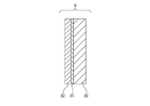
- the X-ray emitting device 13 includes a housing 11 having an emission window 10, an X-ray emission source 1, and a drive circuit 14.
- the X-ray emission source 1 includes an envelope 6 having an X-ray transmission window 9.
- the inside of the envelope 6 is a decompressed (vacuumed) internal space 12.
- the internal space 12 may have a degree of vacuum at which an electron can fly at least a distance between an electron emission source 3 described later and an X-ray emitting target 8 (hereinafter abbreviated to a target) as an electron mean free path.
- the degree of vacuum may be 1E-4 Pa or less.
- the degree of vacuum can be arbitrarily selected considering an electron emission source to be used, an operating temperature, and the like.
- the degree of vacuum When a cold cathode electron emission source is used, it is more preferable to set the degree of vacuum to 1E-6 Pa or less. In order to maintain the degree of vacuum, it is possible to install a getter (not shown in Fig. 1) in the internal space 12 or in an auxiliary space (not shown in Fig. 1) connected to the internal space 12.
- the electron emission source 3 disposed in the envelope 6 may be an electron emission source whose emission amount of electrons can be controlled from outside the envelope 6.
- a hot cathode electron emission source or a cold cathode electron emission source can be arbitrarily used as the electron emission source 3.
- the electron emission source 3 is electrically connected to the drive circuit 14 installed outside the envelope 6 so that the amount of emission electrons and an on/off state of electron emission can be controlled via a current introduction terminal 4 disposed to penetrate the envelope 6.
- the electron emission source 3 includes an electron emission unit 2.
- the electrons emitted from the electron emission unit 2 become an electron beam 5 having energy of 100 keV to 200 keV by an extraction grid and an acceleration electrode (not shown in Fig. 1) and can enter the target 8 disposed to face the electron emission unit 2.
- the extraction grid and the acceleration electrode can be embedded in an electron gun tube of a hot cathode. It is possible to dispose a correction electrode for adjusting an irradiation spot position of the electron beam and astigmatism of the electron beam in the electron emission source 3 and connect the correction electrode to a correction circuit (not shown in Fig. 1) disposed inside or outside the housing 11.
- the housing 11 is desired to be set to a predetermined potential and the housing 11 can be grounded via a grounding terminal 16.
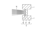
- the target 8 is disposed in a vacuum atmosphere in the envelope 6 and disposed at a position where the electron beam 5 from the electron emission source 3 can enter one surface of the target 8.
- the target 8 is formed by a target material including heavy elements. X-rays are generated in a process in which electrons of the incident electron beam lose kinetic energy in the target material. Specifically, an area of "electron penetration length multiplied by electron beam spot" in the target material is the X-ray generation area and X-rays are emitted in all directions from the X-ray generation area.
- an X-ray component of the generated X-rays which is emitted from the reverse surface of the electron incident surface, is used.
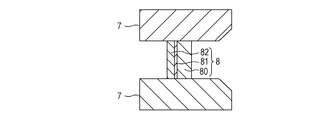
- the target 8 is fixed to a target holding unit 7.
- the electron emission source 3, the target 8, and an emitted X-ray extraction section (the transmission window 9 and the emission window 10) are arranged so that the centers of these are aligned on the same straight line.
- the target holding unit 7 can double as an electrical connection mechanism for setting the target to a predetermined potential so that the accelerated electron beam 5 enters the target 8. Therefore, the target holding unit 7 is desired to be formed of a material having heat resistance for maintaining stable positioning performance and electrical conductivity for maintaining electrical connection performance even when the temperature of the target portion varies.
- the target holding unit 7 can include an aperture mechanism, that is, an X-ray shielding function, which defines an externally extracted component 15 of the emitted X-rays.
- the target holding unit 7 is further desired to have heat resistance, electrical conductivity, and high specific gravity for shielding the X-rays.
- heavy metals such as molybdenum, tantalum, and tungsten, that is, metals of atomic number of 30 or more, can be used for the target holding unit 7.
- the target holding unit 7 has a target holding surface 7C that defines the position of the target 8 and a relative angle to the electron emission source. Further, the target holding unit 7 has a portion protruding from the target holding surface 7C toward the electron emission source 3 and this portion is referred to as a rear target holding unit 7A. Further, the target holding unit 7 has a portion protruding from the target holding surface 7C toward the emission window 10 and this portion is referred to as a front target holding unit 7B.
- the rear target holding unit 7A is formed of a high specific gravity material, it is possible to limit the emission range of reflection electrons generated in the target 8 and X-rays emitted toward the electron emission source 3.
- the front target holding unit 7B is formed of a high specific gravity material, it is possible to limit the emission range of X-rays generated in the target 8 and emitted toward the X-ray transmission window 9.
- a case in which a high specific gravity material is provided to the housing 11 and the envelope 6 which are located apart from the target 8 and whose heights are high a case in which a high specific gravity material is provided to the target holding unit 7B which is located nearer the target 8 has an effect for suppressing increase in the weight of the entire X-ray emitting device and has an advantage in weight saving.
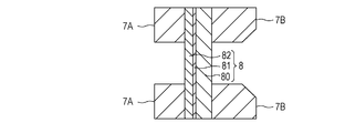
- the target 8 will be described in more detail with reference to Fig. 2.
- the target 8 includes a diamond substrate 80, a first layer 81 including a metal where the standard free energy of formation of carbide in a temperature range from 500 degrees Celsius to 1500 degrees Celsius is negative, and a second layer 82 including a metal whose atomic number is 42 or more, which are laminated in this order.
- the diamond substrate 80 includes at least a surface (inner surface) to which the first layer 81 and the second layer 82 are provided, a surface (outer surface) which is the reverse surface of the inner surface and from which the X-rays are extracted, and side surfaces for connecting to the target holding unit 7.
- the thickness (the distance between the inner surface and the outer surface) of the diamond substrate 80 is desired to be substantially constant within the surfaces in order to uniformize the transmittance distribution of the X-rays.
- the diamond substrate 80 can have a cylindrical shape (disk shape) or a flat plate shape. It is possible to determine the upper limit of the thickness of the diamond substrate 80 from the viewpoint of the transmittance of the X-rays and determine the lower limit of the diamond substrate 80 from the viewpoint of the heat transfer properties and the strength.
- the diamond substrate 80 having a thickness from 50 micrometer to 2000 micrometer can be used. More preferably, the diamond substrate 80 having a thickness from 350 micrometer to 1200 micrometer can be used.
- the diamond substrate 80 may be any of a single crystal body, a polycrystalline body, and an amorphous body such as a diamond-like carbon (DLC), the diamond substrate 80 is desired to be a single crystal body from the viewpoint of thermal conductivity.
- a method for manufacturing the diamond substrate 80 can be any of a chemical vapor deposition (CVD) method, a sintered body formation method, and a high pressure synthesis method in which the diamond substrate 80 is synthesized using a seed crystal, a carbon raw material, and a catalytic metal under high pressure.
- the method is not particularly limited, the high pressure synthesis method is desired to be used from the viewpoint of securing the thickness, the thermophysical property, and the degree of purity.
- the second layer 82 As a second metal included in the second layer 82, a material having high specific gravity is used to efficiently convert incident electrons into X-rays.
- the second layer 82 includes a metal whose atomic number is 42 or more.
- tungsten, ruthenium, platinum, iridium, and tantalum can be used.
- An area where electrons are converted into X-rays is also an area where heat is generated and a local heat generation spot occurs in a range of the electron penetration length in the layer thickness direction.
- the second layer 82 formed of a material having high thermal conductivity has an advantage in heat transfer properties to the target holding unit 7 which is colder than the heat generating portion, so that it is possible to alleviate overheating of an electron irradiation spot 53.
- the tungsten has a high melting point of 3380 degrees Celsius and the tungsten is a material having high thermal conductivity larger than 100 W/mK in a wide temperature range, so that the tungsten is one of more desired materials.
- the film thickness of the second layer 82 can be selected from the viewpoint of the amount of generation, the amount of attenuation, and the radiation quality of the X-rays, the acceleration voltage of the electrons, and the heat transfer to the target holding unit.
- the thickness can be selected from a range between 1 micrometer and 15 micrometer.
- the film thickness of the second layer 82 can be larger than the electron penetration length.
- the film thickness of the second layer 82 can be smaller than the electron penetration length.
- a method for forming the second layer 82 is not limited to a specific method if the adhesion to the diamond substrate and the first layer is secured. Sputtering, CVD, vapor deposition, and the like can be used as the method for forming the second layer 82.
- the first layer 81 will be described.
- Diamond is excellent as the diamond substrate and the transmission window of the X-rays from the viewpoint of high thermal conductivity, high thermostability, and low specific gravity.
- the affinity between diamond and various metal materials having a high specific gravity which can be applied to the target material is low, so that there is an adhesion problem that a film is peeled when a film of the target metal (the second layer 82) is formed and when an X-ray emitting operation is performed.
- the first layer 81 is disposed between the diamond substrate 80 and the second layer 82 as an adhesion layer in order to improve the adhesion problem.
- the first layer 81 includes a first metal that forms a carbide with diamond, so that the first layer 81 can secure the adhesion to the diamond layer.
- the first layer 81 is formed of a material where the standard free energy of formation of carbide is negative.
- the standard free energy of formation of carbide is a free energy change when the carbide is generated from a single body (metal).
- the standard free energy of formation of carbide generally has temperature characteristic.
- the temperature range concerning the standard free energy of formation of carbide in the present invention is 500 degrees Celsius to 1500 degrees Celsius considering the operating temperature of the target and the melting point of the metal included in the second layer.
- the standard free energy of formation of the carbide in the first layer of the present invention is preferred to be negative because it is possible to obtain an anchoring effect between the first layer 81 and the diamond substrate 80. It is more preferable that the standard free energy of formation of the carbide in the first layer of the present invention is 40 kJ/mol degree Celsius or less because when the standard free energy of formation of the carbide is 40 kJ/mol degree Celsius or less, it is possible to obtain a sufficient anchoring effect between the first layer 81 and the diamond substrate 80 even when the layer thickness of the first layer 81 is thin. Further, it is more preferable that the metal included in the second layer and the metal included in the first layer form a solid solution because a high affinity between the first layer 81 and the second layer 82 can be used. From the same viewpoint, it is more preferable that the metal included in the second layer and the metal included in the first layer are in a relationship of complete solid solution.
- the second layer 82 is formed of tungsten
- titanium, vanadium, tantalum, or chromium is applied as the first layer 81
- metallic elements included in the second layer 82 and metallic elements included in the first layer 81 can form a solid solution at an arbitrary composition ratio.
- a continuous metal density distribution is formed on an interface between the layers formed of materials that can form a solid solution at an arbitrary composition ratio, so that the two layers can be firmly and closely adhered to each other at the interface thereof.
- an embodiment of the present invention includes that the metal elements included in the first layer 81 satisfy that the standard free energy of formation of carbide in the temperature range between 500 degrees Celsius and 1500 degrees Celsius is negative, so that it is possible to secure the adhesion between the first layer 81 and the diamond substrate 80.
- titanium, vanadium, tantalum, or chromium is applied as the first layer 81, so that the metal elements included in the first layer 81 satisfy that the standard free energy of formation of carbide in the temperature range between 500 degrees Celsius and 1500 degrees Celsius is 40 kJ/mol degree Celsius or less and it is possible to further secure the adhesion between the first layer 81 and the diamond substrate 80.
- first layer 81 titanium or tantalum is applied as the first layer 81, so that the metal elements satisfy that the standard free energy of formation of carbide is 100 kJ/mol degree Celsius or less and it is possible to further more secure the adhesion between the first layer 81 and the diamond substrate 80.
- a method for forming the first layer 81 is not limited to a specific method if the adhesion to the diamond substrate 80 and the second layer 82 is secured.
- Various film forming methods such as Sputtering, CVD, and vapor deposition can be used as the method for forming the first layer 81.
- the first metals included in the first layer 81 are excellent in adhesion as described above, as shown in Table 1, the thermal conductivity of these metals is not necessarily higher than that of tungsten suitable for the second layer 82.
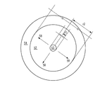
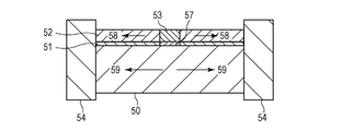
- Figs. 5A and 5B are illustrations for explaining a heat transfer path.
- Fig. 5A is a top view and Fig. 5B is a cross-sectional view corresponding to the top view.
- a first layer 51 having a layer thickness t 1 and a second layer 52 having a layer thickness t 2 are laminated on a diamond substrate 50 having a thickness t 0 and a disk shape of radius r 2 so that each layer covers the layer below including the circumferential portion thereof.
- the laminated target is fixed by a target holding unit 54 at the circumferential portion of each layer.
- a high temperature portion corresponding to the electron irradiation spot in the second layer is shown as a heating portion 53 of the first layer.
- the heating portion 53 is shown as a circle of radius r 1 which is concentric with the outer circumferential circle of the second layer 82.
- a low temperature portion target holding unit 54.
- the thermal conductivities of the diamond substrate 50, the first layer 51, and the second layer 52 are defined as lambda 0 , lambda 1 , and lambda 2 respectively.
- the heat transfer rate K 1 of a heat flow path through which heat flows from the heating portion 53 in the second layer 52 to the diamond substrate 50 via the heat transfer path in the first layer immediately below the heating portion 53 is obtained by Formula 1.
- the heat transfer rate K 2 of a heat flow path 58 through which heat is radially transferred from the heating portion 53 in the second layer 52 in the film surface direction to the low temperature portion 54 is obtained by Formula 2.
- the heat transfer rate K 0 of a heat flow path 59 through which heat received from the first layer 51 by the diamond substrate 50 at the center of the diamond substrate 50 is radially transferred from the center of the diamond substrate 50 in the substrate surface direction to the low temperature portion 54 is obtained by Formula 3.
- a condition that satisfies a continuous heat flow relation of the heat flow paths 57, 58, and 59 and a condition that the heat flow path 57 does not become a bottleneck (a narrow or obstructed section, where movement is slowed down) of heat transfer from the heating portion 53 to the diamond substrate 50 are represented by Formula 4.
- the substrate is formed of diamond having high thermal conductivity lambda 0 , so that the relationship between the thermal conductivity lambda 0 and the thermal conductivity lambda 1 of the second layer 52 satisfies Formula 5.
- Formula 6 has a technical meaning that resolves the thermal bottleneck of the first layer 51 and enables the diamond substrate 50 having higher thermal conductivity to be a dominant heat transfer path.
- Formula 6 means that it is possible to resolve the thermal bottleneck of the first layer 51 by further reducing the upper limit of the layer thickness of the first layer 51 when the layer thickness of the second layer 52 is large. By doing so, even when the electron irradiation density to the target metal layer (the second layer 52) increases, it is possible to obtain an effect that the overheating of the heating portion 53 in the second layer 52, which is an X-ray emission spot, can be alleviated.
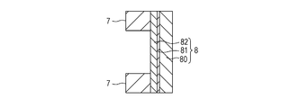
- the shape of the lamination of the first layer 81 and the second layer 82 with respect to the diamond substrate 80 is not limited to the shape which covers the entire one side of the diamond substrate 80 as shown in Fig. 2, but includes various covering shapes as shown in Figs. 3B to 3D. How much of the first layer 81 and the second layer 82 is covered can be determined considering the irradiation range of an electron beam 35 and the electrical connection with the target holding unit 7 as shown in Fig. 3A. As a method for fixing the target 8 of the present invention to the target holding unit 7, it is possible to use a method using a conductive connection member such as silver solder not shown the drawings or a pressure bonding method.
- a conductive connection member such as silver solder not shown the drawings or a pressure bonding method.
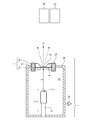
- the shape of the X-ray emitting unit including the target holding unit 7 and the target 8 is not limited to the shape shown in Fig. 1, but the X-ray emitting unit can have various shapes as shown in Figs. 4A to 4D.
- the shape by which the target holding unit 7 holds the target 8 can be appropriately determined considering the electrical connection to the target 8, the range in which reflection electrons reflected by the second layer 82 of the target 8 reach, and the emission ranges of the emitted X-rays and backscattering X-rays.
- the present invention includes not only that a single electron emission source 3 and a single X-ray emitting target 8 are arranged for the X-ray emitting device 13 and the X-ray emission source 1 as shown in Fig. 1, but also that a plurality of electron emission sources 3 and a plurality of X-ray emitting targets 8 are arranged.
- a potential relationship between the electron emission source 3 and the X-ray emitting target 8 can be arbitrarily selected based on the potential of the housing 11, the type of the power supply circuit, and the like.
- the potential relationship between the electron emission source 3 and the X-ray emitting target 8 may be determined so that the accelerated electron beam 5 can enter the target 8 with a predetermined kinetic energy.
- Example 1 will be described in detail with reference to Figs. 2, 4B, and 6.
- the diamond substrate 80 has a disk shape (a cylindrical shape) with a diameter of 5 mm and a thickness of 1 mm.
- the thermal conductivity of the diamond substrate 80 at room temperature is 2000 W/mK.
- Organic substances on the surface of the diamond substrate 80 are removed in advance by UV-ozone asher.
- the first layer 81 of titanium having a thickness of 10 nm is formed on one surface of two circular surfaces with a diameter of 1 mm of the diamond substrate by a sputtering method using Ar as carrier gas.
- the substrate is heated so that the temperature of the diamond substrate is 260 degrees Celsius when the titanium film is formed.
- the second layer 82 of tungsten having a thickness of 8 micrometer is formed on the first layer 81 by a sputtering method using Ar as carrier gas by continuous deposition without venting atmosphere in a film forming device.
- the substrate is heated by a stage so that the temperature of the diamond substrate 80 is 260 degrees Celsius when the tungsten film is formed in the same manner as when the titanium film is formed.
- the thermal conductivity of each layer is evaluated using a monitor substrate prepared in advance in the film forming process. As a result, the thermal conductivity of the first layer is 16 W/mK and the thermal conductivity of the second layer is 178 W/mK.
- the thicknesses of the first layer 81 and the second layer 82 before the layers are laminated, calibration curve data of a film thickness and a film forming time when a single layer film is formed is obtained for each layer in advance, and the first layer 81 and the second layer 82 are laminated so that films having selected film thicknesses are formed based on the film forming times.
- the film thicknesses for obtaining the calibration curve data are measured using a spectroscopic ellipsometer UVISEL ER manufactured by Horiba, Ltd.
- a cross-section of the obtained target 8 is mechanically polished and processed by FIB, so that a cross-section analyte S1 including interfaces between the second layer 82, the first layer 81, and the diamond substrate 80 is prepared.
- Distribution of composition and combination of the prepared analyte S1 is mapped by X-ray photoelectron spectroscopy (XPS) and it is found that there is a combination of titanium and carbon at the boundary between an area where titanium is dominant, which corresponds to the first layer 81, and an area where carbon is dominant, which corresponds to the diamond substrate 80.
- XPS X-ray photoelectron spectroscopy
- a cross-section of the obtained target 8 is processed by FIB, so that an analyte S2 to be observed by a transmission electron microscope (TEM) is prepared in the same manner as the analyte S1. Thereafter, crystalline distribution, crystal orientation distribution, and composition distribution are evaluated by combining a bright-field image observation, an electron diffraction analysis (ED), and an electron spectroscopy analysis of the transmission electron microscope. The obtained crystal orientation distribution is mapped. As a result, it is found that a solid solution of tungsten and titanium is formed in a transition area between an area where tungsten is dominant, which corresponds to the second layer 82 and an area where titanium is dominant, which corresponds to the first layer 81. In this way, as shown in Fig.
- the target 8 is obtained in which the diamond substrate 80, the first layer 81 formed of titanium, and the second layer 82 formed of tungsten are laminated in this order.
- the target 8 is sandwiched and held by the target holding unit 7 formed of tungsten including the rear target holding unit 7A and the front target holding unit 7B.
- the target 8 is fixed so that the second layer 82 is in contact with the rear target holding unit 7A by using silver solder (not shown in the drawings) as a connection layer.
- a unit which includes the target 8 and the target holding unit 7, and the electron emission source 3, which is an impregnated type thermal-electron gun including the electron emission unit 2, are disposed to face each other so that the second layer 82 and the electron emission unit 2 face each other directly.
- the X-ray emitting unit and the electron emission source 3 are disposed in a vacuum chamber 18 including a flange 19.
- the target holding unit 7 is fixed to the vacuum chamber 18 via the flange 19.
- the target 8 is connected to the vacuum chamber 18 via target holding unit 7 and the flange 19 so that the target 8 is electrically conductive to the vacuum chamber 18.
- the potential of the vacuum chamber 18 is set to the ground potential by the ground terminal 16 connected to the vacuum chamber 18.
- the potential of the cathode of the electron emission source 3 is set to -120 kV by a power supply circuit not shown in the drawings, so that the electron emission source 3 can irradiate the electron beam 5 having a kinetic energy of 120 keV to the center of the second layer 82 of the target 8.
- a copper cooling pipe (not shown in the drawings) in which water flows is disposed along the circumferential portion of the electron emission source 3 and the circumferential portion of the rear target holding unit 7A, so that the electron emission source 3, the target 8, and the target holding unit 7 can be cooled down when the X-ray output operation is performed.
- dosimeters (20, 21) are replaceably arranged at a position on an extended line connecting the electron emission source 2 and the center of the target 8 having a disk shape and 100 cm away from the surface of the diamond substrate 80 facing the air.
- One dosimeter 20 is a dosimeter using an ionization chamber method, which is arranged to measure a time-integrated value of the dose.
- the other dosimeter includes a semiconductor detector and is arranged to measure the time variation of the dose. The density of the current emitted from the electron emission source 3 is changed and linearity of X-ray dose with respect to the electron irradiation amount is measured by the dosimeter 20.
- the time variation in one second of the center value of the intensity of the dose detected by the dosimeter 21 is measured.
- the electrons are emitted, the electrons are focused onto the surface of the second layer 82 on the vacuum side.
- the spot radius of the electron beam 5 is 0.5 mm.
- Tables 2 and 3 In both evaluations of linearity and stability, a current flowing from the second layer 82 to the ground electrode is detected and the variation of the current density flowing through the second layer 82 is controlled to be 1% or less by a negative feedback circuit not shown in the drawings.
- Example 2 In the same manner as in Example 1 except that the layer thickness of the first layer 81 is 1 nm and the layer thickness of the second layer 82 is 7 micrometer, the linearity of the X-ray output intensity with respect to the electron irradiation amount and the stability of the X-ray output intensity in a high dose electron irradiation condition are evaluated. The evaluation results are shown in Tables 4 and 5.
- Example 2 In the same manner as in Example 1 except that the layer thickness of the first layer 81 is 100 nm and the layer thickness of the second layer 82 is 5.5 micrometer, the linearity of the X-ray output intensity with respect to the electron irradiation amount and the stability of the X-ray output intensity in a high dose electron irradiation condition are evaluated.
- the evaluation results are shown in Tables 6 and 7.
- Example 2 In the same manner as in Example 1 except that the layer thickness of the first layer 81 is 0.1 nm and the layer thickness of the second layer 82 is 5.6 micrometer, the linearity of the X-ray output intensity with respect to the electron irradiation amount and the stability of the X-ray output intensity in a high dose electron irradiation condition are evaluated.
- the evaluation results are shown in Tables 8 and 9.
- the linearity of the X-ray output intensity with respect to the electron irradiation amount and the stability of the X-ray output intensity in a high dose electron irradiation condition are evaluated.
- the thermal conductivity of the first layer 81 formed of tantalum at room temperature is 58 W/mK. The evaluation results are shown in Tables 10 and 11.
- Example 2 In the same manner as in Example 1 except that the first layer 81 is a tantalum film formed by sputtering and the layer thickness of the first layer 81 is 1 nm, the linearity of the X-ray output intensity with respect to the electron irradiation amount and the stability of the X-ray output intensity in a high dose electron irradiation condition are evaluated.
- the evaluation results are shown in Tables 12 and 13.
- the second layer 82 of the target 8 and the electron emission unit 2 are disposed to face each other in the same manner as in Example 1, and as shown in Fig. 1, the transmission window 9 formed of beryllium having a thickness of 1 mm is disposed and the target 8 and the electron emission source 3 of Example 1 are arranged in the envelope 6 formed of a ceramic of boron nitride.
- the target holding unit 7 is electrically connected to an electrode (not shown in the drawings) provided in advance in the envelope 6 formed of ceramic.
- the surface of the target 8 on which no film is formed faces the air side and the surface of the target 8 on which films are formed faces the vacuum side.
- the transmission window 9, the target 8, and the electron emission unit 2 are fixed so that the center of the transmission window 9, the center of the target 8, and the center of the electron emission unit 2 are aligned on the same straight line.
- the internal space 12 of the envelope 6 is decompressed, so that a vacuum envelope 6 is formed.
- the potential of the electrode (not shown in the drawings) provided in the vacuum envelope 6 is set to the ground potential and the cathode of the electron emission source 3 is set to -120 kV, so that electrons having a kinetic energy of 120 keV can be irradiated to the center of the second layer 82 of the target 8.
- the X-ray emission source 1 including the vacuum envelope 6 and the drive circuit 14 that drives the electron gun are disposed in a housing internal space 17 of the housing 11 filled with insulating silicon oil, so that the X-ray emitting device 13 is completed.
- the linearity of the X-ray output intensity with respect to the electron irradiation amount and the stability of the X-ray output intensity in a high dose electron irradiation condition of the obtained X-ray emitting device 13 are evaluated.
- the evaluation results are shown in Tables 14 and 15. In both evaluations of linearity and stability, a current flowing from the second layer 82 to the ground electrode is detected and the variation of the current density flowing through the second layer 82 is controlled to be 1% or less by a negative feedback circuit not shown in the drawings.
Landscapes
- X-Ray Techniques (AREA)
Abstract
L'invention concerne une cible émettrice de rayons X qui comporte un substrat en diamant (80), une première couche (81) déposée sur le substrat en diamant et comprenant un premier métal, ainsi qu'une deuxième couche (82) déposée sur la première couche et comprenant un deuxième métal dont le numéro atomique est supérieur ou égal à 42 et dont la conductivité thermique est supérieure à celle du premier métal. L'épaisseur de la première couche est supérieure ou égale à 0,1 nm et inférieure ou égale à 100 nm. On empêche la surchauffe de la cible de sorte que les variations de rendement dues à une augmentation de la température sont éliminées. Il est ainsi possible d'émettre des rayons X stables à haut rendement.
Priority Applications (1)
| Application Number | Priority Date | Filing Date | Title |
|---|---|---|---|
| US14/124,400 US20140126701A1 (en) | 2011-06-07 | 2012-05-28 | X-ray emitting target and x-ray emitting device |
Applications Claiming Priority (2)
| Application Number | Priority Date | Filing Date | Title |
|---|---|---|---|
| JP2011-127512 | 2011-06-07 | ||
| JP2011127512A JP2012256443A (ja) | 2011-06-07 | 2011-06-07 | X線放出ターゲットおよびx線放出装置 |
Publications (1)
| Publication Number | Publication Date |
|---|---|
| WO2012169143A1 true WO2012169143A1 (fr) | 2012-12-13 |
Family
ID=46458576
Family Applications (1)
| Application Number | Title | Priority Date | Filing Date |
|---|---|---|---|
| PCT/JP2012/003477 WO2012169143A1 (fr) | 2011-06-07 | 2012-05-28 | Cible émettrice de rayons x et dispositif émetteur de rayons x |
Country Status (3)
| Country | Link |
|---|---|
| US (1) | US20140126701A1 (fr) |
| JP (1) | JP2012256443A (fr) |
| WO (1) | WO2012169143A1 (fr) |
Cited By (1)
| Publication number | Priority date | Publication date | Assignee | Title |
|---|---|---|---|---|
| CN106783487A (zh) * | 2013-01-18 | 2017-05-31 | 佳能株式会社 | 透射型x射线靶和包括该透射型x射线靶的放射线产生管 |
Families Citing this family (3)
| Publication number | Priority date | Publication date | Assignee | Title |
|---|---|---|---|---|
| JP6140983B2 (ja) * | 2012-11-15 | 2017-06-07 | キヤノン株式会社 | 透過型ターゲット、x線発生ターゲット、x線発生管、x線x線発生装置、並びに、x線x線撮影装置 |
| JP6207246B2 (ja) * | 2013-06-14 | 2017-10-04 | キヤノン株式会社 | 透過型ターゲットおよび該透過型ターゲットを備える放射線発生管、放射線発生装置、及び、放射線撮影装置 |
| EP3599619A1 (fr) * | 2018-07-25 | 2020-01-29 | Siemens Healthcare GmbH | Cible de production de rayons x, émetteur de rayons x et procédé de production de rayons x |
Citations (5)
| Publication number | Priority date | Publication date | Assignee | Title |
|---|---|---|---|---|
| JP2000306533A (ja) | 1999-02-19 | 2000-11-02 | Toshiba Corp | 透過放射型x線管およびその製造方法 |
| JP2003505845A (ja) | 1999-07-26 | 2003-02-12 | フラウンホーファー−ゲゼルシャフト ツル フェルデルング デル アンゲヴァンテン フォルシュング エー ファウ | X線陽極およびその製造法 |
| EP1580787A2 (fr) * | 2004-03-26 | 2005-09-28 | Shimadzu Corporation | dispositif generateur des rayons X |
| US7359487B1 (en) * | 2005-09-15 | 2008-04-15 | Revera Incorporated | Diamond anode |
| EP2048689A1 (fr) * | 2007-10-11 | 2009-04-15 | Kratos Analytical Limited | Électrode pour appareil de rayons X |
Family Cites Families (2)
| Publication number | Priority date | Publication date | Assignee | Title |
|---|---|---|---|---|
| EP0432568A3 (en) * | 1989-12-11 | 1991-08-28 | General Electric Company | X ray tube anode and tube having same |
| JP2002042705A (ja) * | 2000-07-28 | 2002-02-08 | Toshiba Corp | 透過放射型x線管およびその製造方法 |
-
2011
- 2011-06-07 JP JP2011127512A patent/JP2012256443A/ja not_active Withdrawn
-
2012
- 2012-05-28 WO PCT/JP2012/003477 patent/WO2012169143A1/fr active Application Filing
- 2012-05-28 US US14/124,400 patent/US20140126701A1/en not_active Abandoned
Patent Citations (5)
| Publication number | Priority date | Publication date | Assignee | Title |
|---|---|---|---|---|
| JP2000306533A (ja) | 1999-02-19 | 2000-11-02 | Toshiba Corp | 透過放射型x線管およびその製造方法 |
| JP2003505845A (ja) | 1999-07-26 | 2003-02-12 | フラウンホーファー−ゲゼルシャフト ツル フェルデルング デル アンゲヴァンテン フォルシュング エー ファウ | X線陽極およびその製造法 |
| EP1580787A2 (fr) * | 2004-03-26 | 2005-09-28 | Shimadzu Corporation | dispositif generateur des rayons X |
| US7359487B1 (en) * | 2005-09-15 | 2008-04-15 | Revera Incorporated | Diamond anode |
| EP2048689A1 (fr) * | 2007-10-11 | 2009-04-15 | Kratos Analytical Limited | Électrode pour appareil de rayons X |
Cited By (2)
| Publication number | Priority date | Publication date | Assignee | Title |
|---|---|---|---|---|
| CN106783487A (zh) * | 2013-01-18 | 2017-05-31 | 佳能株式会社 | 透射型x射线靶和包括该透射型x射线靶的放射线产生管 |
| CN106783487B (zh) * | 2013-01-18 | 2018-10-19 | 佳能株式会社 | 透射型x射线靶和包括该透射型x射线靶的放射线产生管 |
Also Published As
| Publication number | Publication date |
|---|---|
| JP2012256443A (ja) | 2012-12-27 |
| US20140126701A1 (en) | 2014-05-08 |
Similar Documents
| Publication | Publication Date | Title |
|---|---|---|
| US9281158B2 (en) | X-ray emitting target and X-ray emitting device | |
| US9257254B2 (en) | Transmissive target, X-ray generating tube including transmissive target, X-ray generating apparatus, and radiography system | |
| JP5911323B2 (ja) | ターゲット構造体及びそれを備える放射線発生装置並びに放射線撮影システム | |
| EP2740331B1 (fr) | Appareil de génération de rayonnement et appareil d'imagerie par rayonnement | |
| US9029795B2 (en) | Radiation generating tube, and radiation generating device and apparatus including the tube | |
| US9552956B2 (en) | Radiation generating apparatus and radiation imaging apparatus | |
| WO2013031423A1 (fr) | Tube générateur de rayonnement et appareil d'imagerie à rayonnement utilisant ce tube | |
| US9653249B2 (en) | Transmission type target, radiation generating tube having the transmission type target, radiation generator having the radiation generating tube, and radiation imaging apparatus having the radiation generator | |
| JP2013051153A5 (fr) | ||
| EP2751827A1 (fr) | Générateur de rayons x et appareil d'imagerie à rayons x | |
| JP5925219B2 (ja) | 放射線ターゲット、放射線発生管、放射線発生装置、放射線撮影システム及びその製造方法 | |
| US10229808B2 (en) | Transmission-type target for X-ray generating source, and X-ray generator and radiography system including transmission-type target | |
| JP2014026801A (ja) | 穿刺用x線発生装置 | |
| WO2012169143A1 (fr) | Cible émettrice de rayons x et dispositif émetteur de rayons x | |
| JP6153314B2 (ja) | X線透過型ターゲット及びその製造方法 | |
| JP2017139238A (ja) | 透過型ターゲットおよび該透過型ターゲットの製造方法、ならびに、放射線発生管、並びに、該放射線発生管を備えた放射線発生装置、並びに、該放射線発生装置を備えた放射線撮影装置 | |
| JP6381756B2 (ja) | 透過型ターゲットおよび該透過型ターゲットを備える放射線発生管、放射線発生装置、及び、放射線撮影装置 |
Legal Events
| Date | Code | Title | Description |
|---|---|---|---|
| 121 | Ep: the epo has been informed by wipo that ep was designated in this application |
Ref document number: 12732717 Country of ref document: EP Kind code of ref document: A1 |
|
| WWE | Wipo information: entry into national phase |
Ref document number: 14124400 Country of ref document: US |
|
| NENP | Non-entry into the national phase |
Ref country code: DE |
|
| 122 | Ep: pct application non-entry in european phase |
Ref document number: 12732717 Country of ref document: EP Kind code of ref document: A1 |