WO2012169014A1 - インピーダンス整合装置、制御方法 - Google Patents
インピーダンス整合装置、制御方法 Download PDFInfo
- Publication number
- WO2012169014A1 WO2012169014A1 PCT/JP2011/063069 JP2011063069W WO2012169014A1 WO 2012169014 A1 WO2012169014 A1 WO 2012169014A1 JP 2011063069 W JP2011063069 W JP 2011063069W WO 2012169014 A1 WO2012169014 A1 WO 2012169014A1
- Authority
- WO
- WIPO (PCT)
- Prior art keywords
- value
- power transmission
- circuit
- matching
- input impedance
- Prior art date
- Legal status (The legal status is an assumption and is not a legal conclusion. Google has not performed a legal analysis and makes no representation as to the accuracy of the status listed.)
- Ceased
Links
Images


















Classifications
-
- H—ELECTRICITY
- H03—ELECTRONIC CIRCUITRY
- H03H—IMPEDANCE NETWORKS, e.g. RESONANT CIRCUITS; RESONATORS
- H03H7/00—Multiple-port networks comprising only passive electrical elements as network components
- H03H7/38—Impedance-matching networks
- H03H7/40—Automatic matching of load impedance to source impedance
-
- H—ELECTRICITY
- H01—ELECTRIC ELEMENTS
- H01F—MAGNETS; INDUCTANCES; TRANSFORMERS; SELECTION OF MATERIALS FOR THEIR MAGNETIC PROPERTIES
- H01F38/00—Adaptations of transformers or inductances for specific applications or functions
- H01F38/14—Inductive couplings
-
- H—ELECTRICITY
- H02—GENERATION; CONVERSION OR DISTRIBUTION OF ELECTRIC POWER
- H02J—ELECTRIC POWER NETWORKS; CIRCUIT ARRANGEMENTS OR SYSTEMS FOR SUPPLYING OR DISTRIBUTING ELECTRIC POWER; SYSTEMS FOR STORING ELECTRIC ENERGY
- H02J50/00—Circuit arrangements or systems for wireless supply or distribution of electric power
- H02J50/10—Circuit arrangements or systems for wireless supply or distribution of electric power using inductive coupling
-
- H—ELECTRICITY
- H02—GENERATION; CONVERSION OR DISTRIBUTION OF ELECTRIC POWER
- H02J—ELECTRIC POWER NETWORKS; CIRCUIT ARRANGEMENTS OR SYSTEMS FOR SUPPLYING OR DISTRIBUTING ELECTRIC POWER; SYSTEMS FOR STORING ELECTRIC ENERGY
- H02J50/00—Circuit arrangements or systems for wireless supply or distribution of electric power
- H02J50/10—Circuit arrangements or systems for wireless supply or distribution of electric power using inductive coupling
- H02J50/12—Circuit arrangements or systems for wireless supply or distribution of electric power using inductive coupling of the resonant type
-
- H—ELECTRICITY
- H02—GENERATION; CONVERSION OR DISTRIBUTION OF ELECTRIC POWER
- H02J—ELECTRIC POWER NETWORKS; CIRCUIT ARRANGEMENTS OR SYSTEMS FOR SUPPLYING OR DISTRIBUTING ELECTRIC POWER; SYSTEMS FOR STORING ELECTRIC ENERGY
- H02J50/00—Circuit arrangements or systems for wireless supply or distribution of electric power
- H02J50/80—Circuit arrangements or systems for wireless supply or distribution of electric power involving the exchange of data, concerning supply or distribution of electric power, between transmitting devices and receiving devices
-
- H—ELECTRICITY
- H02—GENERATION; CONVERSION OR DISTRIBUTION OF ELECTRIC POWER
- H02J—ELECTRIC POWER NETWORKS; CIRCUIT ARRANGEMENTS OR SYSTEMS FOR SUPPLYING OR DISTRIBUTING ELECTRIC POWER; SYSTEMS FOR STORING ELECTRIC ENERGY
- H02J50/00—Circuit arrangements or systems for wireless supply or distribution of electric power
- H02J50/90—Circuit arrangements or systems for wireless supply or distribution of electric power involving detection or optimisation of position, e.g. alignment
-
- H—ELECTRICITY
- H04—ELECTRIC COMMUNICATION TECHNIQUE
- H04B—TRANSMISSION
- H04B5/00—Near-field transmission systems, e.g. inductive or capacitive transmission systems
- H04B5/70—Near-field transmission systems, e.g. inductive or capacitive transmission systems specially adapted for specific purposes
- H04B5/79—Near-field transmission systems, e.g. inductive or capacitive transmission systems specially adapted for specific purposes for data transfer in combination with power transfer
Definitions
- the present invention relates to a wireless contactless power transmission system, and more particularly to an impedance matching device useful for a wireless power transmission system based on the principle of electromagnetic resonance coupling (also called magnetic field resonance or electric field resonance).
- non-contact power transmission technology that does not require connection of an AC (Alternating Current) cable or the like has begun to be used when supplying power to home appliances, industrial devices, electric vehicles, and the like.
- AC Alternating Current
- non-contact charging devices are widely used for small devices around water such as electric toothbrushes and shavers, and portable devices such as mobile phones.
- a system for charging or supplying electric power in a non-contact manner from an electric power supply device placed under the vehicle body has been put into practical use for an electric vehicle stopped at a parking lot or a bus stop.
- the electromagnetic induction method is widely used for the above-mentioned household use, industrial use, and electric vehicle, and has been widely commercialized from a low power of several W to a high power of several tens kW.
- the electromagnetic induction method it is necessary to reduce the distance (air gap, hereinafter referred to as “gap”) between the power transmission side coil (primary side coil) and the reception side coil (secondary side coil) as much as possible.
- Gap air gap
- SPS Small Power
- Non-Patent Document 1 Non-Patent Document 2, and Patent Document 1
- This method is characterized by a large gap between the transmitting and receiving antennas (several tens of centimeters to several meters) and resistance to misalignment, and it can be applied in a wide range of applications such as household equipment, industrial equipment, and electric vehicles.
- the electromagnetic resonance coupling method is also highly expected to supply power wirelessly to a moving body as an area impossible by electromagnetic induction.
- Patent Document 3 discloses a technique for adjusting impedance based on a distance between antennas or a load.
- Non-Patent Document 3 describes the usefulness of the magnetic field resonance method, etc.
- Non-Patent Document 4 describes the validity as a model of a power transmission / reception antenna based on the electromagnetic resonance method of a series-parallel type equivalent circuit. There is description about.
- the applicant has filed applications of International Application No. PCT / JP2010 / 063569 and International Application No. PCT / JP2010 / 063570 as applications related to the present application.
- the wireless power transmission system based on the electromagnetic resonance method is (A) When the coupling state between the power transmission and power reception antennas changes, the value of the input impedance at the power transmission antenna end changes. (B) The power reception antenna side Even when the value of the load connected to fluctuates, the input impedance value at the power transmission antenna end changes. Therefore, when the above coupling state changes or when the load value changes, impedance mismatch occurs between the output impedance of the power transmission circuit (power supply) and the power transmission antenna input end, and reflection loss occurs. . As a result, the transmission efficiency is deteriorated. In order to suppress reflection loss due to impedance mismatching, an impedance matching circuit is generally used. However, there is no impedance matching device that can efficiently and quickly cope with the change in input impedance peculiar to the electromagnetic resonance method.
- the present invention has been made to solve the above-described problems, and an object thereof is to provide an impedance matching device capable of matching impedances efficiently and at high speed.
- the invention according to claim 1 is an impedance matching device installed between a power transmission circuit and the power transmission antenna in a wireless power transmission system that transmits power by coupling a power transmission antenna and a power reception antenna with an electromagnetic field.
- Input impedance estimation means for estimating an input impedance of the power transmission antenna or an input impedance equivalent value corresponding to the input impedance, a variable inductor element inserted in series between the power transmission circuit and the power transmission antenna, A variable capacitor element connected in parallel to the power transmission antenna with respect to the variable inductor element; and a variable inductor element inserted in series between the power transmission circuit and the power transmission antenna; Possible to be connected in parallel to the power transmission circuit side than the variable inductor element.
- a second matching circuit including a capacitor element, a through circuit inserted in series between the power transmission circuit and the power transmission antenna, and a circuit connected to the power reception antenna and consuming the transmitted power
- a load value estimating means for estimating a load value, and a control value corresponding to an inductance value and a capacitance value necessary for matching with a predetermined impedance value using the first or the second matching circuit; Based on the load value and the input impedance equivalent value, the first matching circuit, the second matching circuit, and the input impedance equivalent value.
- the data is stored in the storage unit. Reading the control value, and having a control value output means for outputting to the selected circuit by the control value the circuit selection means.
- the invention according to claim 4 is an impedance matching device installed between a power transmission circuit and the power transmission antenna in a wireless power transmission system that transmits power by coupling a power transmission antenna and a power reception antenna with an electromagnetic field.
- Input impedance estimation means for estimating an input impedance of the power transmission antenna or an input impedance equivalent value corresponding to the input impedance, a variable inductor element inserted in series between the power transmission circuit and the power transmission antenna, A variable capacitor element connected in parallel to the power transmission antenna with respect to the variable inductor element; and a variable inductor element inserted in series between the power transmission circuit and the power transmission antenna; Possible to be connected in parallel to the power transmission circuit side than the variable inductor element.
- a second matching circuit including a capacitor element, a through circuit inserted in series between the power transmission circuit and the power transmission antenna, and a coupling for estimating a coupling coefficient between the power transmission antenna and the power reception antenna
- a control value corresponding to an inductance value and a capacitance value necessary for matching with a predetermined impedance value using the coefficient estimation means and the first or second matching circuit is obtained as the coupling coefficient and the input impedance equivalent value.
- One of the first matching circuit, the second matching circuit, and the through circuit based on the storage unit that is pre-stored in correspondence with the input signal, the coupling coefficient, and the input impedance equivalent value.
- the control value stored in the storage unit is determined. Out, and having a control value output means for outputting to the selected circuit by the control value the circuit selection means.
- the invention according to claim 10 is a wireless power transmission system that transmits power by coupling a power transmitting antenna and a power receiving antenna with an electromagnetic field, and is installed between a power transmitting circuit and the power transmitting antenna, and
- a first matching circuit comprising: a variable inductor element inserted in series with a power transmission antenna; and a variable capacitor element connected in parallel to the power transmission antenna with respect to the variable inductor element; and the power transmission circuit
- a second matching circuit comprising: a variable inductor element inserted in series with the power transmission antenna; and a variable capacitor element connected in parallel to the power transmission circuit with respect to the variable inductor element; and the power transmission circuit
- a control value corresponding to an inductance value and a capacitance value necessary for matching with a power value corresponds to a load value of the circuit connected to the power receiving antenna and consuming the transmitted power and an input impedance equivalent value.
- One of the first matching circuit, the second matching circuit, and the through circuit based on a load value estimating step for estimating a load value, and the load value and the input impedance equivalent value A circuit selection step of electrically connecting the load, the load value, and the input impedance equivalent value, Based on, and having a control value output step of outputting the control value stored in the storage unit read, the control value to the circuit selected by the circuit selecting step.
- the invention according to claim 11 is a wireless power transmission system that transmits power by coupling a power transmitting antenna and a power receiving antenna with an electromagnetic field, and is installed between a power transmitting circuit and the power transmitting antenna, and
- a first matching circuit comprising: a variable inductor element inserted in series with a power transmission antenna; and a variable capacitor element connected in parallel to the power transmission antenna with respect to the variable inductor element; and the power transmission circuit
- a second matching circuit comprising: a variable inductor element inserted in series with the power transmission antenna; and a variable capacitor element connected in parallel to the power transmission circuit with respect to the variable inductor element; and the power transmission circuit
- a storage unit that stores in advance a control value corresponding to an inductance value and a capacitance value necessary for matching with a power value in association with a coupling coefficient between the power transmission antenna and the power reception antenna and the input impedance
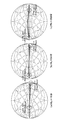
- FIG. 7 is a diagram in which a locus of input impedance when a load value is fixed and a coupling coefficient between a power transmission / reception antenna is changed in a range of “0.311 to 0.021” is plotted on a Smith chart.
- FIG. 7 is a diagram in which a locus of input impedance when a coupling coefficient k between a power transmission / reception antenna is fixed and a load value is changed in a range of “5 ⁇ ” to “500 ⁇ ” is plotted on a Smith chart.
- the graph of the ratio of the electric power which entered the power transmission antenna with respect to the electric power supplied from a power supply is shown.
- a matching circuit for matching the input impedance at the end of the power transmission antenna to 50 ⁇ is shown. It is a figure which shows the ratio of the electric power which entered the power transmission antenna 3 with respect to the electric power supplied from the power supply 20 in the state which added the matching circuit of FIG.
- (A) shows the state of the power entering the power transmission antenna with respect to the power supplied from the power source when the coupling coefficient remains “0.1” and the load value decreases to “10 ⁇ ” from the matching state shown in FIG. Indicates the ratio.
- (B) shows the power that enters the power transmission antenna for the power supplied from the power source when the coupling coefficient k remains “0.1” and the load value increases to “200 ⁇ ” from the matching state shown in FIG. The ratio is shown.
- (A) shows the ratio of the power entering the power transmission antenna with respect to the power supplied from the power source when the load value remains “50 ⁇ ” and the coupling coefficient decreases to “0.05” from the matching state.
- FIG. 3 is a diagram in which the Smith chart is roughly divided into two areas, area A and area B. An example of transition from each point on the impedance locus existing in the region A or region B to the matching point is shown.
- A It is an example of the matching circuit of the 1st form.
- B An example of a second type matching circuit.
- (A) is a graph of “1-
- the graph of a waveform and a reflected wave voltage waveform is shown.
- (A) shows a graph of “1-
- the graph of the traveling wave voltage waveform and reflected wave voltage waveform in is shown.
- FIG. 4 is a flowchart illustrating a processing procedure of flow 1 in the first embodiment.
- 4 is a flowchart illustrating a processing procedure of flow 2 in the first embodiment.
- 5 is a flowchart illustrating a processing procedure of flow 3 in the first embodiment.
- 6 is a flowchart illustrating a processing procedure of a flow 4 in the first embodiment. It is a schematic block diagram of the electric power transmission system which concerns on 2nd Example.
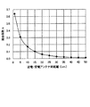
- the graph which shows the relationship between the distance of a power transmission antenna and a power receiving antenna, and a coupling coefficient is shown.
- An example of the alignment correction amount table corresponding to the case where the coupling coefficient is “0.07” is shown.
- An example of a matching circuit suitable for the embodiment is shown.
- required by theoretical calculation in 2nd Example is shown. It is an example of reflection loss reduction at the time of implementing an impedance matching process using a matching correction amount table. It is the graph shown about the relationship of the traveling wave voltage waveform and reflected wave voltage waveform in case the load shifts
- (A) is a graph of “1-
- the graph of a waveform and a reflected wave voltage waveform is shown.
- (A) shows a graph of “1-
- the graph of a wave voltage waveform and a reflected wave voltage waveform is shown.
- FIG. 24A shows a graph of “1-
- FIG. 24B shows a traveling wave voltage waveform and a reflected wave voltage waveform at the driving frequency in FIG. A graph is shown.
- it is a flowchart showing a processing procedure of flow 5.
- it is a flowchart showing the processing procedure of flow 6.
- it is a flowchart showing the processing procedure of flow 7. It is a figure which shows the structure of the matching circuit which concerns on a modification.
- an impedance matching device installed between a power transmitting circuit and the power transmitting antenna.
- An input impedance estimating means for estimating an input impedance of the power transmission antenna or an input impedance equivalent value corresponding to the input impedance, and a variable inductor element inserted in series between the power transmission circuit and the power transmission antenna;
- a variable capacitor element connected in parallel to the power transmission antenna with respect to the variable inductor element, and a variable inductor element inserted in series between the power transmission circuit and the power transmission antenna
- a second matching circuit including a variable capacitor element, a through circuit inserted in series between the power transmission circuit and the power transmission antenna, and the transmitted power connected to the power reception antenna.
- a load value estimating means for estimating a load value of the circuit, and a control value corresponding to an inductance value and a capacitance value necessary for matching with a predetermined impedance value using the first or the second matching circuit, Based on the load value and the input impedance equivalent value, the first matching circuit and the second matching circuit based on the load value and the input impedance equivalent value in advance. And a circuit selection means for electrically connecting any one of the through circuit, the load value, and the input impedance equivalent value, the memory Having read the stored said control value, the control value output means for outputting the control value to the circuit selected by the circuit selecting unit, to.
- the above-described impedance matching device is installed between a power transmission circuit and a power transmission antenna in a wireless power transmission system that transmits power by coupling a power transmission antenna and a power reception antenna with an electromagnetic field.
- the impedance matching device includes an input impedance estimation unit, first and second matching circuits, a through circuit, a load value estimation unit, a storage unit, a circuit selection unit, and a control value output unit.
- the storage unit associates the control value corresponding to the inductance value and the capacitance value necessary for matching with the predetermined impedance value using the first or second matching circuit with the load value and the input impedance equivalent value. And store in advance.
- control value means an inductance value and a capacitance value, a control voltage value for changing the inductance value and the capacitance value using an electrical or mechanical mechanism such as a motor, a plurality of minute inductor elements, This includes a bit pattern for controlling ON / OFF of a switch unit such as a relay or MEMS (Micro Electro Mechanical System) included in an LC network circuit composed of minute capacitor elements.
- the impedance estimation means estimates an input impedance equivalent value.
- the “input impedance equivalent value” refers to a value corresponding to an input impedance such as a value having a unique relationship with the input impedance in addition to the input impedance of the power transmission antenna.
- the load value estimating means estimates a load value of a circuit connected to the power receiving antenna and consuming the transmitted power.
- the circuit selecting means electrically connects any one of the first matching circuit, the second matching circuit, and the through circuit based on the load value and the input impedance equivalent value.
- the control value output means reads the control value stored in the storage unit based on the load value and the input impedance equivalent value, and outputs the control value to the circuit selected by the circuit selection means.
- the storage unit includes the control value, flag information indicating the first or second matching circuit that reflects the control value, the load value, and the input impedance.
- the circuit selection unit stores the first matching circuit and the second matching circuit based on the flag information determined from the load value and the input impedance equivalent value. Any one of the matching circuits is electrically connected.
- the impedance matching device stores flag information indicating the matching circuit to be used in association with the load value and the input impedance equivalent value in the storage unit in advance, thereby allowing the estimated load value and input impedance to be stored. Based on the equivalent value, a matching circuit to be used accurately and easily can be selected.
- the control value is a value obtained by changing a coupling state between the power transmission antenna and the power receiving antenna after fixing a load value of the circuit. It is set based on the locus of change in input impedance from the circuit to the power transmission antenna.
- the impedance matching device stores the control value set in this way in the storage unit in advance, and performs impedance matching, thereby reducing processing steps and reducing the circuit scale and required memory capacity. Can do.
- an impedance installed between a power transmitting circuit and the power transmitting antenna.
- An input impedance estimating means for estimating an input impedance of the power transmission antenna or an input impedance equivalent value corresponding to the input impedance, and a variable inductor inserted in series between the power transmission circuit and the power transmission antenna
- a first matching circuit including an element and a variable capacitor element connected in parallel to the power transmission antenna with respect to the variable inductor element, and a variable inserted in series between the power transmission circuit and the power transmission antenna Inductor element and parallel to the transmission circuit side of the variable inductor element
- a second matching circuit including a variable capacitor element connected; a through circuit inserted in series between the power transmission circuit and the power transmission antenna; and a coupling coefficient between the power transmission antenna and the power reception antenna
- a coupling coefficient estimating means for estimating a control value corresponding to an inductance value
- the above-described impedance matching device is installed between a power transmission circuit and a power transmission antenna in a wireless power transmission system that transmits power by coupling a power transmission antenna and a power reception antenna with an electromagnetic field.
- the impedance matching device includes an input impedance estimation unit, first and second matching circuits, a through circuit, a coupling coefficient estimation unit, a storage unit, a circuit selection unit, and a control value output unit.
- the storage unit associates a control value corresponding to an inductance value and a capacitance value necessary for matching with a predetermined impedance value by using the first or second matching circuit with a coupling coefficient and an input impedance equivalent value. Store in advance.
- the impedance estimation means estimates the impedance of the power transmission antenna or an input impedance equivalent value corresponding to the impedance.
- the coupling coefficient estimation unit estimates a coupling coefficient between the power transmitting antenna and the power receiving antenna.
- the circuit selection means electrically connects any one of the first matching circuit, the second matching circuit, and the through circuit based on the coupling coefficient and the input impedance equivalent value.
- the control value output means reads the control value stored in the storage unit based on the coupling coefficient and the input impedance equivalent value, and outputs the control value to the circuit selected by the circuit selection means.
- the impedance matching device allows the power transmission antenna and the power receiving antenna to be coupled by an electromagnetic field to perform power transmission, and the coupling coefficient between the power transmitting antenna and the power receiving antenna and the value of the load on the power receiving side. Accordingly, impedance matching between the power transmission circuit and the power transmission antenna is performed, and the power input from the power transmission side can be transmitted to the power reception side without loss.
- the storage unit includes the control value and flag information indicating the first or second matching circuit that reflects the control value, the coupling coefficient, and the input impedance equivalent.
- the circuit selecting means stores the first matching circuit and the second matching circuit based on the flag information determined from the coupling coefficient and the input impedance equivalent value. Are electrically connected to each other.
- the impedance matching apparatus stores flag information indicating a matching circuit to be used in association with the coupling coefficient and the input impedance equivalent value in the storage unit in advance, so that the estimated coupling coefficient and the input impedance equivalent value are stored. Based on the above, it is possible to select a matching circuit to be used accurately and easily.
- the control value is obtained when the load value of the circuit is changed after fixing a coupling state between the power transmission antenna and the power reception antenna. It is set based on the locus of change in input impedance from the circuit to the power transmission antenna.
- a traveling wave / reflected wave extraction unit that extracts a traveling wave voltage corresponding to an output signal from the power transmission circuit and a reflected wave voltage corresponding to a reflected signal from the power transmission antenna.
- a reflection coefficient calculating means for calculating an absolute value of a reflection coefficient or a reflection coefficient absolute value equivalent value corresponding to the absolute value based on the traveling wave voltage and the reflected wave voltage; and
- a phase difference calculating unit that compares the phase with the phase of the reflected wave voltage and calculates a phase difference between the phases; and the input impedance estimating unit includes the reflection coefficient absolute value as the input impedance equivalent value. The equivalent value and the phase difference are estimated.
- the “reflection coefficient absolute value equivalent value” is a value corresponding to the absolute value of the reflection coefficient, such as an absolute value of the reflection coefficient or a value uniquely related to the reflection coefficient. This applies to the absolute value of impedance.
- the impedance matching apparatus can specify the input impedance by estimating the reflection coefficient absolute value equivalent value and the above-described phase difference, and suitably determines a matching circuit to be used and a control value to be applied. be able to.
- a traveling wave / reflected wave extraction unit that extracts a traveling wave voltage corresponding to an output signal from the power transmission circuit and a reflected wave voltage corresponding to a reflected signal from the power transmission antenna.
- a phase difference calculating unit that compares the phase of the traveling wave voltage and the phase of the reflected wave voltage and calculates a phase difference between the phases, and the circuit selecting unit includes an absolute value of the reflection coefficient. If is below a predetermined value, the through circuit is selected.
- the control value is quantized so that the quantization interval becomes smaller as the absolute value of the reflection coefficient becomes larger.
- the power transmission antenna is installed between the power transmission circuit and the power transmission antenna.
- a first matching circuit comprising: a variable inductor element inserted in series between the power transmission circuit and the power transmission antenna; and a variable capacitor element connected in parallel to the power transmission antenna with respect to the variable inductor element;
- a second matching circuit comprising: a variable inductor element inserted in series between the power transmission circuit and the power transmission antenna; and a variable capacitor element connected in parallel to the power transmission circuit side relative to the variable inductor element.
- a through circuit inserted in series between the power transmission circuit and the power transmission antenna, and the first or second matching circuit A control value corresponding to an inductance value and a capacitance value necessary for matching with a constant impedance value, a load value of a circuit connected to the power receiving antenna and consuming the transmitted power, and an input impedance equivalent value,
- a circuit selection step for electrically connecting one, the load value and the input impedance. Based on the dance equivalent value, and a control value output step of outputting the control value stored in the storage unit read, the control value to the circuit selected by the circuit selecting step.
- the power transmission antenna is installed between the power transmission circuit and the power transmission antenna.
- a first matching circuit comprising: a variable inductor element inserted in series between the power transmission circuit and the power transmission antenna; and a variable capacitor element connected in parallel to the power transmission antenna with respect to the variable inductor element;
- a second matching circuit comprising: a variable inductor element inserted in series between the power transmission circuit and the power transmission antenna; and a variable capacitor element connected in parallel to the power transmission circuit side relative to the variable inductor element.
- a through circuit inserted in series between the power transmission circuit and the power transmission antenna, and the first or second matching circuit Control values corresponding to an inductance value and a capacitance value necessary for matching with a constant impedance value are stored in advance in association with the coupling coefficient between the power transmission antenna and the power reception antenna and the input impedance equivalent value.
- FIG. 1 shows an example of a power transmission antenna based on an electromagnetic resonance method and an antenna (power transmission / reception antenna) used as a power reception antenna.
- the power transmission / reception antenna shown in FIG. 1 is an antenna in which windings are spirally formed on two upper and lower planes.
- the diameter of the power transmission / reception antenna is 30 cm, the total number of turns on the upper and lower surfaces is 5.2, the pitch between the windings is 7 mm, and the distance between the upper and lower surfaces is 15 mm.
- the power transmission / reception antenna feeds power from a feeding point 102 located at the center of the upper and lower surface windings.
- the inductance “L” is “8.64 ⁇ H”
- the capacitor “C” is “17.49 pF”
- the loss resistance “R”. was “1.0 ⁇ ”.
- the power transmission / reception antenna operates as a series resonance circuit having these constants.
- FIG. 2 shows a series-parallel equivalent circuit having a capacitor connected in parallel to the series resonant circuit portion, which is an accurate equivalent circuit model of the power transmission / reception antenna of FIG.
- the parallel capacitor “Ct” was “10.08 pF”.
- the antenna shown in FIG. 1 is generally arranged opposite to the power transmission side and the power reception side, respectively.
- a power transmission circuit (power source) is connected to the power transmission antenna, and a load is connected to the power reception antenna by a coaxial cable or the like.
- FIG. FIG. 3 shows a power transmission system in which the antenna shown in FIG. 1 is disposed to face each other as a power transmission antenna and a power reception antenna.
- a power source is connected to the power transmitting antenna, and a load is connected to the power receiving antenna.
- FIG. 4 shows an example in which the power transmission system shown in FIG. 3 is expressed using a series-parallel equivalent circuit expression.
- “Lm” in FIG. 4 represents the mutual inductance in a state where the power transmitting antenna and the power receiving antenna are magnetically coupled.
- the value of the coupling coefficient k is determined by the positional relationship between the power transmitting antenna and the power receiving antenna, such as the gap (gap width) between the power transmitting antenna and the power receiving antenna and the amount of positional deviation. Changing the amount of gap or misalignment may be considered as replacing the value of the coupling coefficient k.
- FIG. 5 shows that the load value RL is fixed to 10 ⁇ in (a), 50 ⁇ in (b), and 200 ⁇ in (c), and the coupling coefficient k between the transmitting antenna and the receiving antenna is “0.311 to 0”.
- .021 is a diagram in which the locus of the input impedance Zin when changed in the range of" 021 "is plotted on the Smith chart.
- the antenna shown in FIG. 1 is a power transmission antenna and a power reception antenna, and the amount of displacement in the horizontal direction is zero
- the coupling coefficient k is fixed to 0.030 in (a), 0.064 in (b), and 0.120 in (c), and the load value RL is “5 ⁇ ” to “500 ⁇ ”. It is the figure which plotted the locus
- the locus of the input impedance Zin is located to the left (see FIG. 5C), and when the load value RL is an intermediate value such as “50 ⁇ ”, the input impedance Zin The trajectory of is distributed almost without any bias.
- the relative position of the locus on the Smith chart is further to the left as the coupling coefficient k is smaller, and to the right as the coupling coefficient k is larger. Therefore, when the coupling coefficient k is a relatively small value such as “0.030”, the locus of the input impedance Zin is located to the right (see FIG. 6A), and the coupling coefficient k is “0.12”.
- the locus of the input impedance Zin is located to the left (see FIG. 6C), and in the case where the coupling coefficient k is an intermediate value such as “0.064”. The locus of the input impedance Zin is distributed almost without any deviation from left to right.
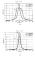
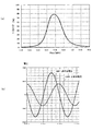
- FIG. 7 shows the ratio of “power entering the power transmission antenna” to “power supplied from the power source” (1 ⁇
- the power transmitting antenna and the power receiving antenna are opposed to each other as shown in FIG. 4, the antenna shown in FIG. 1 is used as the power transmitting antenna and the power receiving antenna, the load value RL is “50 ⁇ ”, and the coupling coefficient k is set to 0.1, that is, the gap corresponds to “15 cm” without positional deviation.
- the above-mentioned ratio at the drive frequency of 12.947 MHz is 89.4%.
- the input impedance Zin at the power transmission antenna end at the drive frequency of 12.947 MHz is “97.86-3.98 j ( ⁇ )”. Therefore, in this case, since the input impedance Zin is not “50 ⁇ ” corresponding to the output impedance of the power transmission circuit, a mismatch loss of about 10% occurs.
- FIG. 8 shows a matching circuit for matching the input impedance Zin at the power transmission antenna end to “50 ⁇ ”.
- FIG. 9 shows a graph of the ratio of the power entering the power transmission antenna to the power supplied from the power source with the matching circuit of FIG. 8 added. As shown in FIG. 9, in the state where the matching circuit of FIG. 8 is added, the above-described ratio at the drive frequency “12.947 MHz” is 100%. In this case, the input impedance Zin at the power transmission antenna end is matched with the output impedance of the power transmission circuit, and no mismatch loss occurs.
- FIG. 10A shows a power transmission antenna for the power supplied from the power source when the coupling coefficient k remains “0.1” and the load value RL decreases to “10 ⁇ ” from the matching state shown in FIG.
- FIG. 10B shows the ratio of the power that has entered, and FIG. 10B shows the power supply when the load value RL increases to “200 ⁇ ” while the coupling coefficient k remains “0.1” from the matching state shown in FIG.
- the ratio of the electric power that has entered the power transmission antenna to the electric power supplied from is shown.
- FIG. 11A shows a power transmission antenna for power supplied from a power source when the load value RL remains “50 ⁇ ” and the coupling coefficient k decreases to “0.05” from the matching state shown in FIG.
- FIG. 11B shows the power supply when the load value RL remains “50 ⁇ ” and the coupling coefficient k increases to “0.15” from the matching state shown in FIG.
- the ratio of the electric power that has entered the power transmission antenna to the electric power supplied from is shown.
- 2 ) at the drive frequency “12.947 MHz” decreases to 65.1% in the case of FIG. In the case of FIG.11 (b), it has fallen to 85.4%.
- the input impedance Zin at the power transmission antenna end is a predetermined (1) coupling coefficient k between the power transmission and power reception antennas.
- (2) Load value RL on the power receiving side Even if a matching circuit that is optimal for the power transmission circuit is added between the power transmission circuit and the power transmission antenna, the load value RL subsequently fluctuates for some reason, or the gap between the power transmission / reception antenna changes and the coupling coefficient When k changes, it deviates from the matching point. As a result, the reflection loss when power is supplied from the power transmission circuit to the power transmission antenna is increased, and transmission efficiency is deteriorated.
- the power transmission system estimates the load value RL and the input impedance Zin of the power transmission antenna end, and refers to a predetermined table (also referred to as “matching correction amount table”) based on these estimated values.
- a predetermined table also referred to as “matching correction amount table”
- the matching circuit to be used and the control value applied to the matching circuit are determined.
- the power transmission system matches the input impedance Zin of the power transmission antenna with the output impedance of the power transmission circuit.
- the power transmission system maintains the matching state by performing a matching tracking operation that continues to maintain the matching state once the matching state is reached.
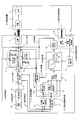
- FIG. 12 is a schematic configuration diagram of the power transmission system according to the first embodiment.
- the power transmission system includes a power transmission side device 1 having a power transmission circuit 2 and a power transmission antenna 3, and a power reception side device 4 having a power reception antenna 5 and a load 6.
- the power transmission circuit 2 includes a power source 20 and an amplification unit 21.
- the amplification unit 21 functions as a control circuit that adjusts the magnitude of power transmitted from the power source 20 and controls a start operation and a stop operation when power is transmitted from the power source 20.
- the first type matching circuit 11 includes a variable inductor element inserted in series between the power transmission circuit 2 and the power transmission antenna 3, and a variable capacitor element connected in parallel to the end on the power transmission antenna 3 side.
- the second type matching circuit 12 includes a variable inductor element inserted in series between the power transmission circuit 2 and the power transmission antenna 3, and a variable capacitor element connected in parallel to the end on the power transmission circuit 2 side.
- the first-type matching circuit 11 and the second-type matching circuit 12 are also simply referred to as “matching circuits”.
- the storage unit 25 stores flag information “If” indicating which matching circuit of the first type matching circuit 11 or the second type matching circuit 12 should be used and a control value “Tc” to be applied to the matching circuit.
- a plurality of determined alignment correction amount tables are stored for each load value.
- a serial number index also referred to as “index Idx”
- the control value Tc is defined in ascending order of the corresponding coupling coefficient k.
- the control value Tc indicates an inductance value (also referred to as “inductance value L”) and a capacitance value (also referred to as “capacitance value C”) set in the matching circuits 11 and 12 of the first type or the second type. .
- the control value Tc is input when the power transmission antenna 3 is viewed from the power transmission circuit 2 when the gaps are changed by making the power transmission antenna 3 and the power reception antenna 5 of the electromagnetic resonance coupling system face each other. It is set based on the locus of change of the impedance Zin.
- the switch units 13 and 14 electrically connect either the first-type matching circuit 11 or the second-type matching circuit 12 or the through circuit 30 made of only electric wires to the power transmission circuit 2 and the power transmission antenna 3.
- the load estimation unit 7 includes a current value detection unit 71, a voltage value detection unit 72, a load value calculation unit 73, and control communication units 74 and 75, and transmits rated power (that is, power to be originally transmitted). Prior to this, a process of calculating an estimated value RL (also referred to as “estimated load value RLe”) of the load 6 of the power receiving side device 4 is performed. Specifically, before transmitting the rated power, when the power transmission antenna 3 transmits a small amount of power, the current value detection unit 71 detects the current flowing through the load 6 and detects the detected current value (“detected current value Ie Is also supplied to the load value calculation unit 73.
- the voltage value detection unit 72 detects a voltage value applied to the load 6 and supplies the detected voltage value (also referred to as “detected voltage value Ve”) to the load value calculation unit 73. Then, the load value calculating unit 73 calculates the estimated load value RLe based on the detected current value Ie supplied from the current value detecting unit 71 and the detected voltage value Ve supplied from the voltage value detecting unit 72. Specifically, the load value calculation unit 73 sets the impedance value calculated by dividing the detected voltage value Ve by the detected current value Ie as the estimated load value RLe.
- control communication unit 74 in the power receiving side device 4 transmits the estimated load value RLe calculated by the load value calculating unit 73 via the control wireless communication prepared independently of the power transmission wireless unit.
- the data is transmitted to the control communication unit 75 in the device 1.
- the estimated load value RLe is supplied to the table selection unit 27.
- the table selection unit 27 selects a matching correction amount table corresponding to the load value closest to the supplied estimated load value RLe from a plurality of matching correction amount tables stored for each load value by the storage unit 25. To do.
- the contents of the alignment correction amount table will be described later.
- the traveling wave / reflected wave extraction unit 15 is preferably a directional coupler.
- the reflection coefficient calculator 17 calculates the absolute value (magnitude)
- the phase difference calculation / determination unit 16 calculates the phase difference “ ⁇ ” between the phase ⁇ 1 of the traveling wave voltage Vf and the phase ⁇ 2 of the reflected wave voltage Vr,
- Z 0 represents the impedance of the matching target.
- the reading position determining unit 24 refers to the matching correction value table selected by the table selecting unit 27, and selects a matching circuit to be used from the row of the matching correction value table having the impedance value closest to the calculated input impedance Zin.
- the indicated flag information If and the control value Tc to be applied to the matching circuit are read out.
- the matching circuit selection unit 23 is based on the flag information If supplied from the reading position determination unit 24, and is either the first type matching circuit 11 or the second type matching circuit 12 or the through circuit 30 composed only of electric wires. Are controlled to be electrically connected to the power transmission circuit 2 and the power transmission antenna 3.
- the control value output unit 26 reflects the control value Tc read by the reading position determination unit 24 on the first-type matching circuit 11 or the second-type matching circuit 12 selected by the matching circuit selection unit 23.
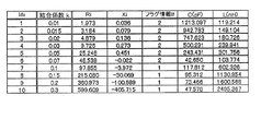
- FIG. 13 shows an example of a matching correction value table corresponding to the case where the load value is “50 ⁇ ”.
- This matching correction table is a capacitance value “C” necessary for matching the input impedance Zin to “50 ⁇ ” when the coupling coefficient k between the power transmitting antenna 3 and the power receiving antenna 5 is in the range of “0.01 to 0.3”.
- an inductance value “L” and flag information If indicating a matching circuit to be used is used.
- the flag information If is “1”
- the flag information If indicates that the matching circuit 11 of the first format should be used
- the flag information If is “2”
- the flag information If is This indicates that the second type matching circuit 12 should be used.
- the reading position determination unit 24 calculates “Ri” and “Xi” (“i” is an index Idx) stored in the matching correction value table and the real part “R” of the calculated input impedance Zin and the imaginary part.
- i is an index Idx
- the part “X” a row having an index Idx that minimizes “(R ⁇ Ri) 2 + (X ⁇ Xi) 2 ” is selected.
- FIG. 13 a row with index Idx “5”, real part Ri “25.248 ⁇ ”, and imaginary part Xi “0.451 ⁇ ” is selected.
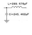
- the readout position determination unit 24 reads out flag information If (here, “2”), which is information related to the format of the matching circuit, from the selected row, supplies the flag information If to the matching circuit selection unit 23, and the capacitance value C “ 243.431 pF ”and the inductance value L“ 301.756 nH ”are read and supplied to the control value output unit 26.
- the matching circuit selection unit 23 operates the switch units 13 and 14 so that the second type matching circuit 12 is connected between the power transmission circuit 2 and the power transmission antenna 3.
- the control value output unit 26 sets the capacitance value C and the inductance value L supplied from the reading position determination unit 24 to the variable capacitor unit and variable inductor unit of the selected matching circuit 12 of the second type.
- FIG. 14 shows the matching circuit determined as described above.
- the power transmission side device 1 refers to the selected matching correction amount table and immediately executes impedance matching between the power transmission circuit 2 and the power transmission antenna 3. I can do it. For example, in the future, when electric vehicles become popular and stop at an intersection, when charging an electric vehicle from a charger installed on the road surface, the charging operation starts as soon as possible after the vehicle stops. Is required. At that time, it is possible to quickly shift to rated power transmission by automatically and quickly performing impedance matching as much as possible.
- phase difference calculation / determination unit 16 the adjustment direction determination unit 18, and the adjustment step width determination unit 19 that perform processing during the alignment follow-up operation after the alignment state is changed from the initial state will be described. A detailed description thereof will be described later in the section [Focus Tracking Operation].
- the phase difference calculation / determination unit 16 specifies the phase relationship between the traveling wave voltage Vf and the reflected wave voltage Vr after the initial state is brought into the matching state. Then, the adjustment direction determination unit 18 uses the row (index Idx) of the matching correction amount table used immediately before as a reference based on the phase relationship between the traveling wave voltage Vf and the reflected wave voltage Vr specified by the phase difference calculation / determination unit 16. Next, the direction of the row from which the control value Tc and the like are read is determined.
- the adjustment step width determination unit 19 determines whether or not the control value Tc to be used needs to be changed from the current control value Tc based on the reflection coefficient absolute value
- the step (movement) width (referred to as “step width Widx”) of the index Idx in the alignment correction table when the new control value Tc is read is determined.
- the reading position determining unit 24 determines a row of the alignment correction amount table from which the control value Tc is read based on the reading direction and the step width Widx determined by the adjustment direction determining unit 18.
- the matching correction amount table used in the present embodiment is characterized in that it is set based on the locus of change of the input impedance Zin at the power transmission antenna end shown in FIGS.
- FIG. 5 shows the locus of the input impedance Zin when the coupling state (that is, the coupling coefficient k) between the power transmission / reception antennas is changed after fixing the value of the load 6 to a certain value.
- FIG. 6 shows a locus of the input impedance Zin when the value RL of the load 6 of the power receiving side device 4 is changed after fixing the coupling state between the power transmission / reception antennas to a certain value.
- the coupling between the power transmission antenna 3 and the power reception antenna 5 increases as the point on the locus of the input impedance Zin approaches the right side of the Smith chart (for example, power transmission / power reception). This corresponds to the fact that the coupling between the antennas becomes weaker (for example, the gap becomes larger).
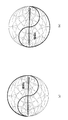
- the Smith chart is roughly divided into two regions, “region A” and “region B”, as shown in FIG. A suitable matching circuit may be used.
- FIG. 16 shows an example of transition from each point on the impedance locus existing in the region A or region B to the matching point “P”.
- the value of the variable capacitor connected in parallel to the power transmission antenna 3 is increased by the correction amount “A1” to increase the point “R”.
- the value of the variable inductor connected in series between the power transmission circuit 2 and the power transmission antenna 3 is increased by the correction amount “A2” and moved to the matching point P. Further, as shown in FIG.
- the value of the variable inductor connected in series between the power transmission circuit 2 and the power transmission antenna 3 is set as the correction amount “
- the value of the variable capacitor connected in parallel to the power transmission circuit 2 side is increased by the correction amount “B2” and moved to the matching point P by increasing it by “B1” and moving to the point “Q”.
- the matching circuit for matching the points on the impedance locus in the region A is as shown in FIG. 17A
- the matching circuit for matching the points on the impedance locus in the region B is as shown in FIG. It is expressed in In this embodiment, the circuit shown in FIG. 17A corresponds to the first type matching circuit 11, and the circuit shown in FIG. 17B corresponds to the second type matching circuit 12. As the matching circuit, these two types of patterns may be prepared.
- the power transmission side device 1 includes the correction amounts A1, A2, and the correction amounts A1 and A2 necessary for matching the points on the impedance locus in the region A by using the first type matching circuit 11 corresponding to FIG.
- the correction amounts B1 and B2 necessary for matching the points on the impedance locus in the region B by using the second type matching circuit 12 corresponding to FIG. 17B are calculated in advance by means such as theoretical calculation or measurement.
- a lookup table in which these values are associated with impedance values, for example, is stored in the storage unit 25 as a matching correction amount table.
- 18A and 18B are diagrams schematically showing a method for obtaining the above-described correction amount by theoretical calculation.
- 18A corresponds to the case where the point on the impedance locus is in the region A
- FIG. 18B corresponds to the case where the point on the impedance locus is in the region B.
- a correction amount “ ⁇ b” is obtained.
- the correction amount ⁇ b and the correction amount ⁇ x correspond to the correction amounts A1 and A2 in FIG. Based on the correction amounts A1 and A2, the capacitance value C and the inductance value L used as the control value Tc are uniquely determined.
- the correction amount ⁇ x and the correction amount ⁇ b correspond to the correction amounts B1 and B2 in FIG.
- the capacitance value C and the inductance value L used as the control value Tc are uniquely determined based on the correction amounts B1 and B2.
- the impedance point Zin on the input impedance locus is paired with the reflection coefficient absolute value
- each impedance point Zin on the input impedance locus is converted into the reflection coefficient absolute value
- a matching correction amount table that associates the value pairs is created in advance.
- are quantized with a resolution required by the application.
- “quantization” delimits the range (value range) of the reflection coefficient absolute value
- is referred to as a “quantization boundary”. Quantization is performed using iterative processing.
- the quantization is performed alternately between the quantization boundary and the representative quantization value so that the reflection coefficient absolute value
- thr preferably corresponds to a value that can suppress the loss due to reflection to 0.5%, that is, a value that can achieve the efficiency of 99.5% if there is no other loss-generating part. It may be set to 0.0707.
- the capacitance value C and the inductance value L to be quantized and stored in the matching correction amount table are determined in this way, the capacitance value C and the inductance value L are quantized as the reflection coefficient absolute value
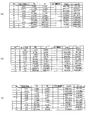
- a correction amount table is shown.
- flag information If designating the type of the matching circuit is also stored.
- the index Idx is a serial number, and a larger index Idx is assigned to a row having a larger coupling coefficient k.
- storage part 25 memorize
- the power transmission side device 1 can determine which matching correction amount table to use based on the estimated load value RLe, and can further determine the power transmission antenna. Based on the input impedance Zin at the end, the matching circuit to be used and the control value Tc set in the matching circuit can be determined by one operation with reference to the selected matching correction amount table.
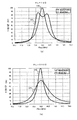
- 20A and 20B show the reflection loss when the impedance matching process is performed using the matching correction amount table shown in FIG. 19A when the value RL of the load 6 is “10 ⁇ ”. It is an example of reduction.
- 20A shows a case where the coupling coefficient k between the power transmitting antenna 3 and the power receiving antenna 5 is “0.064” (gap 20 cm, horizontal displacement 0 cm), and
- FIG. 20B shows the coupling coefficient. The case where k is “0.021” (gap 35 cm, positional deviation 0 cm) is shown.
- the input impedance Zin at the power transmission antenna end is “181.1-j 26.1 ⁇ ”. Therefore, when the line having the closest impedance value is searched in the matching correction amount table shown in FIG. 19A, the line having the index Idx of “6” is selected.
- the flag information If indicating the type of the matching circuit in this row is “1”, and the capacitance value C and the inductance value L are “93.2 pF” and “1136.6 nH”, respectively. As shown in FIG.
- the input impedance Zin at the power transmission antenna end is “20.8 ⁇ j 0.2 ⁇ ”. Accordingly, when a line indicating the closest impedance value in the matching correction amount table shown in FIG. 19A is searched, a line having an index Idx of “3” is selected.
- the flag information If indicating the type of the matching circuit in this row is “2”, and the capacitance value C and the inductance value L are “314.6 pF” and “300.2 nH”, respectively. As shown in FIG.
- the power transmission side device 1 of the first embodiment obtains the estimated load value RLe by storing the matching correction amount table for each value RL of the load 6 of the reception side device 4 in the storage unit 25.
- an appropriate matching circuit can be configured automatically and at high speed by a single operation.
- This operation is an operation for maintaining the matching state after taking impedance matching once.
- an automatic matching operation is performed (generally, this operation is performed with the output reduced), and the value RL of the load 6 of the power receiving side device 4
- an optimum matching circuit is configured for the input impedance Zin determined by the coupling state between the power transmitting antenna 3 and the power receiving antenna 5.
- the power transmission circuit 2 shifts to rated power transmission.
- the relative positional relationship between the power transmission side device 1 and the power reception side device 4 changes during power transmission in a state of matching. Such a situation may occur when power transmission is to be performed on a moving object such as an electric vehicle.
- the input impedance Zin at the power transmission antenna end is different from the value obtained when matching is performed by the automatic matching operation earlier, and the matching is again performed. It will shift. In this case, it is necessary to detect the deviation from the matching state as soon as possible and to match again with the changed input impedance Zin.
- the matching tracking operation of the first embodiment follows the change in the coupling state between the power transmitting antenna 3 and the power receiving antenna 5 and appropriately sets the type of matching circuit and the control value Tc applied to the matching circuit. Thus, the alignment state is maintained.
- the matching tracking operation also uses the input impedance locus (see FIG. 5) at the power transmission antenna end when the coupling state (gap or the like) between the power transmission antenna 3 and the power receiving antenna 5 used in the automatic matching operation is changed.
- the input impedance locus shown in FIG. 5 is obtained by changing the coupling state after fixing the value RL of the load 6 of the power receiving side device 4, and this impedance locus is used in the first embodiment.
- the power transmission side device 1 continues to refer to the alignment correction amount table used in the automatic alignment operation, and the row (that is, the index of the alignment correction amount table to be applied). Idx) may be changed.
- the power transmission side device 1 determines whether the state shifted from the matching state with respect to a certain impedance value is shifted to the left or right side on the impedance locus shown in FIG. In other words, the right side is a stronger direction), in other words, the upper side of the alignment correction table currently used is shifted to the upper or lower side (the upper side is the direction in which the coupling is weaker, the lower side is the direction in which it is stronger) Change the configuration of the matching circuit in the direction.
- the index Idx is a serial number, and a larger index Idx is assigned to a row having a larger coupling coefficient k. ing.
- FIGS. 21A to 21C show the relationship between the traveling wave voltage waveform and the reflected wave voltage waveform when the coupling is deviated in a stronger direction.
- FIG. 21A when the value RL of the load 6 is “10 ⁇ ”, matching is achieved in a state where the coupling coefficient k between the power transmitting antenna 3 and the power receiving antenna 5 is “0.064”. Later, a traveling wave voltage waveform and a reflected wave voltage waveform when the coupling coefficient k is sequentially increased to “0.08”, “0.12”, and “0.2” are shown.
- FIG. 21B shows a case where the matching coefficient k is obtained after matching is performed in a state where the coupling coefficient k between the power transmitting antenna 3 and the power receiving antenna 5 is “0.064” when the value RL of the load 6 is “50 ⁇ ”.
- the traveling wave voltage waveform and the reflected wave voltage waveform are shown in the case where is gradually strengthened as “0.08”, “0.12”, “0.2”.
- FIG. 21 (c) shows a case where the matching coefficient k is obtained after matching is performed with the coupling coefficient k between the power transmission antenna 3 and the power receiving antenna 5 being “0.064” when the value RL of the load 6 is “200 ⁇ ”.
- the traveling wave voltage waveform and the reflected wave voltage waveform are shown in the case where is gradually strengthened as “0.08”, “0.12”, “0.2”.
- FIGS. 22A to 22C show the relationship between the traveling wave voltage waveform and the reflected wave voltage waveform when the coupling is shifted in the weakening direction.
- FIG. 22A when the value RL of the load 6 is “10 ⁇ ”, matching is achieved in a state where the coupling coefficient k between the power transmitting antenna 3 and the power receiving antenna 5 is “0.064”. Later, a traveling wave voltage waveform and a reflected wave voltage waveform when the coupling coefficient k is sequentially weakened to “0.055”, “0.04”, and “0.02” are shown.
- FIG. 22B shows a case where the matching coefficient k is obtained after matching is performed in a state where the coupling coefficient k between the power transmitting antenna 3 and the power receiving antenna 5 is “0.064” when the value RL of the load 6 is “50 ⁇ ”.
- the traveling wave voltage waveform and the reflected wave voltage waveform are shown in the case where is gradually weakened as “0.055”, “0.04”, “0.02”.
- FIG. 22C illustrates a case where the matching coefficient k is obtained after matching is performed in a state where the coupling coefficient k between the power transmitting antenna 3 and the power receiving antenna 5 is “0.064” when the value RL of the load 6 is “200 ⁇ ”.
- the traveling wave voltage waveform and the reflected wave voltage waveform are shown in the case where is gradually weakened as “0.055”, “0.04”, “0.02”.
- the power transmission side device 1 continuously monitors the phase relationship between the traveling wave voltage Vf and the reflected wave voltage Vr after having matched once, and reflects the reflected wave with respect to the phase of the traveling wave voltage Vf.
- the phase of the voltage Vr is delayed, it is determined that the coupling between the power transmitting antenna 3 and the power receiving antenna 5 is strengthened.
- the power transmission side device 1 exists in the direction in which the coupling coefficient k increases in the matching correction amount table, that is, in the direction below the current row in the matching correction amount table (direction in which the index Idx increases).
- the control value Tc of the row is set in the matching circuit indicated by the flag information If of the row.
- the power transmitting side device 1 determines that the coupling between the power transmitting antenna 3 and the power receiving antenna 5 is weakened. In this case, the power transmission side device 1 is present in the direction in which the coupling coefficient k decreases in the matching correction value table, that is, in the direction above the current row in the matching correction amount table (the direction in which the index Idx decreases). With reference to the row, the control value Tc of the row is set in the matching circuit indicated by the flag information If of the row.
- the power transmission side device 1 continues to maintain the matching state even when the coupling state between the power transmission antenna 3 and the power reception antenna 5 changes and the input impedance Zin at the power transmission antenna end changes. I can do it.
- the power transmission side device 1 always monitors the reflection coefficient absolute value
- the matching tracking operation is not performed, and when the reflection coefficient absolute value
- the configuration of the matching circuit is changed by changing the row used in the matching correction amount table.
- the power transmission side device 1 can always keep the reflection coefficient absolute value
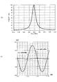
- FIG. 23A shows a graph of “1-
- FIG. 24A shows a graph of “1-
- FIG. 25A shows a graph of “1-
- the power transmission side device 1 detects that the coupling state has changed based on the phase relationship between the traveling wave voltage Vf and the reflected wave voltage Vr. Specifically, the power transmission side device 1 determines that the coupling is strengthened because the phase of the reflected wave voltage Vr is delayed from the traveling wave voltage Vf. Therefore, in this case, the power transmission side device 1 updates the configuration of the matching circuit based on the row in the direction in which the coupling is strengthened in the matching correction amount table, that is, the row with the index Idx “7” larger than the current index Idx “6”. To do. As a result, as illustrated in FIGS. 25A and 25B, the power transmission side device 1 transitions to a state in which matching is achieved again.
- Step width determination method Next, a method for determining the step width Widx based on the reflection coefficient absolute value
- the step width Widx is fixed to “1”.
- the reflection coefficient changes abruptly, if the index Idx is shifted one by one and the control value Tc is updated, it may take a considerable time to reach the index Idx related to the desired control value Tc.
- a gap change or a positional deviation between the power transmission antenna 3 and the power reception antenna 5 occurs at a high speed and with a large fluctuation range. there's a possibility that.
- the power transmission side device 1 preferably determines the step width Widx flexibly according to the change width of the reflection coefficient absolute value
- the power transmission side device 1 stores a table of appropriate step widths Widx corresponding to the variation widths of the respective reflection coefficient absolute values
- the above table is created in advance based on, for example, experiments.
- the power transmission side apparatus 1 determines the step width Widx with reference to this table from the variation width of the reflection coefficient absolute value
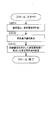
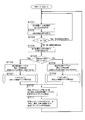
- FIG. 26 is a flowchart illustrating a processing procedure executed by the power transmission side device 1 in the first embodiment.
- the power transmission side apparatus 1 performs the process of the flow 1 of FIG. 26 at a predetermined timing.
- the matching circuit selection unit 23 of the power transmission side device 1 sets the switch units 13 and 14 to the through circuit 30 (step S101). And the power transmission circuit 2 of the power transmission side apparatus 1 outputs minute electric power from the power transmission antenna 3 prior to transmission of rated power (step S102).
- the power transmission side device 1 transmits a signal requesting the power reception side device 4 to estimate the value RL of the load 6 via the control communication unit 75 (step S103). After that, the power receiving side device 4 that has received the signal executes the processing of the flow 2 described later. And the power transmission side apparatus 1 determines whether load estimation was completed (step S104). Specifically, the power transmission side device 1 determines whether or not the estimated load value RLe is received from the power reception side device 4 via the control communication unit 75. And when load estimation is not completed (step S104; No), the power transmission side apparatus 1 continues monitoring whether load estimation is completed.
- step S104 when load estimation is completed (step S104; Yes), the table selection part 27 of the power transmission side apparatus 1 selects the matching correction amount table corresponding to the load value nearest to the estimated load value RLe (step S105). . And the power transmission side apparatus 1 starts the process (automatic alignment process) equivalent to the flow 3 mentioned later (step S106).
- FIG. 27 is a flowchart illustrating a processing procedure executed by the load estimation unit 7 of the power receiving side device 4 in the first embodiment.
- the load estimation unit 7 executes the process of flow 2 in FIG. 27 when a signal to request the estimation of the load value is received from the control communication unit 75 in step S103 in FIG.
- the load estimation unit 7 measures the voltage of the load 6 and the current flowing through the load 6 (step S201). Specifically, the current detection unit 71 detects the detection current value Ie, and the voltage value detection unit 72 detects the detection voltage value Ve. And the load estimation part 7 estimates the value RL of the load 6 (step S202). Specifically, the load value calculating unit 73 of the load estimating unit 7 calculates the estimated load value RLe by dividing the detected voltage value Ve by the detected current value Ie. And the load estimation part 7 transmits estimated load value RLe to the power transmission side apparatus 1 via the control communication part 74 (step S203).
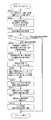
- FIG. 28 is a flowchart illustrating the processing procedure of the flow 3 executed by the power transmission side device 1 in the first embodiment.
- the power transmission side device 1 executes the process of the flow 3 in FIG. 28 when the process proceeds to step S106 in the flow 1 of FIG.
- the matching circuit selection unit 23 of the power transmission side device 1 connects the switch units 13 and 14 to the through circuit 30 and outputs minute power from the power transmission antenna 3 (step S301).
- the reflection coefficient calculation unit 17 of the power transmission side device 1 measures the magnitudes of the traveling wave voltage Vf and the reflected wave voltage Vr extracted by the traveling wave / reflected wave extraction unit 15 (step S302). Then, the reflection coefficient calculation unit 17 calculates the reflection coefficient absolute value
- the power transmission side device 1 determines whether or not the reflection coefficient absolute value
- the power transmission side device 1 determines that it is already in the matching state and does not need to be matched. Then, the process of the flowchart ends.
- step S304 when the reflection coefficient absolute value
- the reading position determination unit 24 searches and selects a row having an impedance value closest to the calculated input impedance Zin from the matching correction amount table selected in the flow 1 (step S308). Then, the reading position determination unit 24 supplies flag information If of the selected row to the matching circuit selection unit 23, and determines a matching circuit to be used (step S309). Further, the control value output unit 26 determines the capacitance value C and the inductance value L of the selected row as the control value Tc to be used (step S310). Then, the control value output unit 26 sets the capacitance value C and the inductance value L in the selected matching circuit (step S311). Then, the matching circuit selection unit 23 connects the switch units 13 and 14 to the matching circuit used based on the flag information If (step S312).
- FIG. 29 is a flowchart illustrating a processing procedure executed by the power transmission side device 1 in the first embodiment.
- the power transmission side device 1 executes the process of the flow 4 in FIG. 29 after the execution of the flow 3.
- the reflection coefficient calculation unit 17 of the power transmission side device 1 measures the magnitudes of the traveling wave voltage Vf and the reflected wave voltage Vr extracted by the traveling wave / reflected wave extraction unit 15 (step S401). Then, the reflection coefficient calculation unit 17 calculates the reflection coefficient absolute value
- the power transmission side device 1 determines whether or not the reflection coefficient absolute value
- the power transmission side device 1 determines that the reflection coefficient absolute value
- the power transmission side device 1 determines that it is already in the matching state and does not need to be matched. Then, the process is returned to step S401, and it is continuously monitored whether the reflection coefficient absolute value
- the phase difference calculation / determination unit 16 specifies the phase relationship between the traveling wave voltage Vf and the reflected wave voltage Vr (Ste S404). Specifically, the phase difference calculation / determination unit 16 determines whether or not the reflected wave voltage Vr is behind the traveling wave voltage Vf (step S405).
- the adjustment direction determination unit 18 determines the reading direction of the matching correction amount table as a direction corresponding to the case where the connection is strengthened (step S406). That is, the adjustment direction determination unit 18 sets the reading direction in the direction in which the index Idx increases in the alignment correction amount table shown in FIG. Then, the adjustment step width determination unit 19 determines the step width Widx according to the reflection coefficient absolute value
- the adjustment direction determination unit 18 determines the reading direction of the matching correction amount table to be a direction corresponding to the case where the connection is weakened (step S408). That is, the adjustment direction determination unit 18 sets the reading direction in the direction in which the index Idx becomes smaller in the alignment correction amount table shown in FIG. Then, the adjustment step width determination unit 19 determines the step width Widx according to the reflection coefficient absolute value
- the reading position determination unit 24 specifies the index Idx of the row to be read from the already selected matching correction amount table based on the specified reading direction and the step width Widx (step S410). ). Then, the control value output unit 26 reads the capacitance value C and the inductance value L from the identified index Idx row, and sets these values in the matching circuit identified from the flag information If in the identified index Idx row. . In addition, the matching circuit selection unit 23 switches the switch units 13 and 14 as necessary based on the flag information If (step S411). And the power transmission side apparatus 1 returns a process to step S401.
- steps S407 and S409 are not indispensable processes, and when a predetermined value is used as the step width Wdix, the power transmission side device 1 does not need to execute the processes in steps S407 and S409. Good.
- the power transmission system estimates the coupling coefficient k and the input impedance Zin of the transmitting antenna end, and refers to the matching correction amount table based on these estimated values, and the matching circuit to be used and the matching circuit A control value Tc to be applied to is determined. Thereby, the power transmission system matches the input impedance Zin of the power transmission antenna with the output impedance of the power transmission circuit. In addition, the power transmission system maintains the matching state by performing a matching tracking operation that continues to maintain the matching state once the matching state is reached.
- FIG. 30 is a schematic configuration diagram of a power transmission system according to the second embodiment.
- the second embodiment differs from the first embodiment in that the value RL of the load 6 changes and the storage unit 25 stores a matching correction amount table when the value RL of the load 6 changes for each coupling coefficient k. .
- the power transmission side device 1 performs the automatic matching operation from the initial state and performs the matching tracking operation after the automatic matching operation.
- the same parts as those in the first embodiment are denoted by the same reference numerals as appropriate, and the description thereof is omitted.
- the coupling coefficient estimation unit 8 performs processing for estimating the coupling coefficient k between the power transmission antenna 3 and the power reception antenna 5 prior to transmission of the rated power.
- the distance sensor 81 measures the distance between the power transmission side device 1 and the power reception side device 4.
- the distance coupling coefficient conversion unit 82 refers to the distance and coupling coefficient k conversion table stored in advance in the memory, and calculates the coupling coefficient k from the distance measured by the distance sensor 81.
- FIG. 31 is a graph showing the relationship between the distance between the power transmitting antenna 3 and the power receiving antenna 5 and the coupling coefficient k.
- the distance coupling coefficient conversion unit 82 stores in advance a conversion table indicating the correspondence between the distance and the coupling coefficient k as shown in FIG.
- the table selection unit 27 uses matching corrections to be used from a plurality of matching correction amount tables stored for each value of the coupling coefficient k in the storage unit 25 based on the coupling coefficient estimation value ke calculated by the coupling coefficient estimation unit 8. Select the quantity table.
- FIG. 32 shows an example of the alignment correction amount table corresponding to the case where the coupling coefficient k is “0.07”.
- An inductance value L is stored.
- the matching correction amount table also stores flag information If indicating which of the first type matching circuit 11 and the second type matching circuit 12 should be used, as in the first embodiment.
- the matching circuit selector 23 switches the switches 13 and 14 so that the second-type matching circuit 12 is connected between the power transmission circuit 2 and the power transmission antenna 3. To work. Further, the capacitance value C and the inductance value L are passed to the control value output unit 26, and the control value output unit 26 sets these values in the variable capacitor unit and variable inductor unit of the selected matching circuit.
- FIG. 33 shows the matching circuit determined as described above.
- the power transmission side device 1 immediately checks the input impedance Zin of the power transmission antenna end and refers to the selected matching correction amount table to immediately transmit the power transmission circuit 2 and Impedance matching between the power transmission antennas 3 can be achieved.
- the charging operation starts as soon as possible after the vehicle stops. Is required.
- the impedance matching is automatically and as quickly as possible, so that it is possible to quickly shift to rated power transmission.
- FIG. 6 shows an input impedance locus when the value RL of the load 6 is changed while the coupling coefficient k between the power transmitting antenna 3 and the power receiving antenna 5 is fixed.
- the matching correction amount is based on the impedance locus shown in FIG. 6 below. A case where the table is configured will be described.
- the Smith chart is roughly divided into two regions, region A and region B.
- a suitable matching circuit may be used. That is, the same idea as the first embodiment can be applied to the second embodiment.
- the value of the variable capacitor connected in parallel to the power transmission antenna 3 is increased by the correction amount A1 and moved to the point R, and then Further, the value of the variable inductor connected in series between the power transmission circuit 2 and the power transmission antenna 3 may be increased by the correction amount A2 and moved to the matching point P.
- the value of the variable inductor connected in series between the power transmission circuit 2 and the power transmission antenna 3 is increased by the correction amount B1 and moved to the point Q, and then parallel to the power transmission circuit 2 side.
- the value of the variable capacitor connected to is increased by the correction amount B2 and moved to the matching point P.
- the form of the matching circuit for matching the impedance points existing in each of the regions A and B is the same as that of the first embodiment, and already shown in FIGS. 17 (a) and 17 (b). .
- FIG. 17A corresponds to the first type matching circuit 11
- FIG. 17B corresponds to the second type matching circuit 12. Accordingly, also in the second embodiment, the power transmission side device 1 may prepare these two patterns of matching circuits as matching circuits.
- the method for creating the alignment correction amount table is the same as in the first embodiment.
- Correction amounts B1 and B2 necessary for matching are obtained in advance by means such as theoretical calculation (see FIGS. 18A and 18B) or measurement, and these values obtained are correlated with, for example, impedance values.
- the up table is stored in advance in the storage unit 25 as an alignment correction table. By doing in this way, the power transmission side apparatus 1 can obtain
- a matching correction amount table obtained by theoretical calculation is shown.
- the index Idx is a serial number, and a larger index Idx is assigned to a line having a larger impedance value (load).
- the storage unit 25 stores a matching correction amount table group for each coupling coefficient k created in this way.
- the power transmission side device 1 determines which matching correction amount table is to be used by obtaining the coupling coefficient k between the power transmitting antenna 3 and the power receiving antenna 5. By obtaining the value of the input impedance Zin at the power transmission antenna end, the matching circuit to be used and the control value Tc set in the matching circuit can be determined from the selected matching correction amount table in one operation.
- FIGS. 35A and 35B show the reflection loss when the impedance matching process is performed using the matching correction amount table shown in FIG. 34B when the coupling coefficient k is “0.07”. It is an example of reduction.
- FIG. 35A shows a case where the value RL of the load 6 is “15 ⁇ ”
- FIG. 35B shows a case where the value RL of the load 6 is “200 ⁇ ”.
- the input impedance Zin of the power transmission antenna end is “150.3 ⁇ j 17.05 ⁇ ”. Therefore, when the line having the closest impedance value in the matching correction amount table shown in FIG. 34B is searched, the line having the index Idx of “2” is selected.
- the flag information If indicating the type of the matching circuit in this row is “1”, and the capacitance value C and the inductance value L are “106.3 pF” and “879.1 nH”, respectively. As shown in FIG.
- the input impedance Zin at the power transmission antenna end is “13.1 + j 1.8 ⁇ ”. Accordingly, when a line indicating the closest impedance value in the matching correction amount table shown in FIG. 34B is searched, a line having an index Idx of “9” is selected.
- the flag information If indicating the type of the matching circuit in this row is “2”, and the capacitance value C and the inductance value L are “412.9 pF” and “247.7 nH”, respectively. As shown in FIG.
- the power transmission side device 1 stores the matching correction amount table for each coupling coefficient k between the power transmission antenna 3 and the power receiving antenna 5 in the storage unit 25, and thereby the coupling coefficient estimated value ke.
- the matching correction amount table By selecting the matching correction amount table to be used and then obtaining the input impedance Zin of the power transmission antenna end, it is possible to automatically and quickly configure an appropriate matching circuit in one operation. .
- This operation is an operation for maintaining the matching state after taking impedance matching once.
- an automatic matching operation is performed (generally, this operation is performed with the output reduced), and the value RL of the load 6 of the power receiving side device 4
- an optimum matching circuit is configured for the input impedance Zin determined by the coupling state between the power transmitting antenna 3 and the power receiving antenna 5.
- the power transmission circuit 2 shifts to rated power transmission.
- the value RL of the load 6 of the power receiving side device 4 changes during power transmission in a matched state.
- the charging operation is generally performed while changing a charging operation mode such as a constant current mode, a constant voltage mode, or a constant power mode.
- a charging operation mode such as a constant current mode, a constant voltage mode, or a constant power mode.
- the load value may change depending on the amount of electricity stored in the battery, it is necessary to assume a load fluctuation in such an application example.
- the value RL of the load 6 of the power receiving side device 4 is changed, the input impedance Zin at the power transmission antenna end is different from the value obtained when matching is performed by the automatic matching operation earlier, and the matching is shifted again. In this case, it is necessary to detect the deviation from the matching state as soon as possible and to match again with the changed input impedance Zin.
- the matching follow-up operation of the second embodiment follows the fluctuation of the value RL of the load 6 of the power receiving side device 4 and appropriately sets the type of the matching circuit and the control value Tc applied to the matching circuit. Thus, the alignment state is maintained.
- the matching tracking operation also uses the input impedance locus (see FIG. 6) at the power transmission antenna end when the value RL of the load 6 used in the automatic matching operation is changed.
- the input impedance locus shown in FIG. 6 is obtained by changing the value RL of the load 6 of the power receiving side device 4 after fixing the coupling coefficient k between the power transmitting antenna 3 and the power receiving antenna 5, which is the second embodiment. In the example, this impedance locus is used.
- the coupling coefficient k between the power transmitting antenna 3 and the power receiving antenna 5 does not change, the input impedance Zin at the power transmitting antenna end exists on the impedance locus shown in FIG.
- the type of matching circuit required for matching an arbitrary impedance point on the impedance locus and the control value Tc applied to the matching circuit are matching corrections generated for each coupling coefficient k as illustrated in FIG. It is stored in the quantity table. Therefore, in the alignment follow-up operation performed once the alignment state is obtained, the power transmission side device 1 continues to refer to the alignment correction amount table used in the automatic alignment operation, and the row (that is, the index of the alignment correction amount table to be applied). Idx) may be changed.
- the power transmission side device 1 has shifted from the matching state with respect to a certain impedance value to the left or right side on the impedance locus shown in FIG. Direction, the direction where the right side becomes smaller), in other words, whichever side of the alignment correction table row currently used is shifted upward or downward (the lower side is the direction in which the load increases, the upper side is the direction in which the upper side is smaller) Then, change the configuration of the matching circuit in an appropriate direction.
- the index Idx is a serial number, and a larger index Idx is assigned to a line having a larger impedance value (load).
- FIGS. 36A to 36C show the relationship between the traveling wave voltage waveform and the reflected wave voltage waveform when the load is shifted in the increasing direction.
- FIG. 36A shows that when the coupling coefficient k is “0.030”, after matching is performed in a state where the value RL of the load 6 is “50 ⁇ ”, the value RL of the load 6 is changed to “ The traveling wave voltage waveform and the reflected wave voltage waveform in the case of increasing sequentially such as “100”, “200”, “400” are shown.
- FIG. 36B shows that when the coupling coefficient k is “0.064” and the matching is performed in a state where the value RL of the load 6 is “50 ⁇ ”, the value RL of the load 6 is set to “100”, “200”. ”,“ 400 ”, the traveling wave voltage waveform and the reflected wave voltage waveform when sequentially increased are shown.
- FIG. 36C shows that when the coupling coefficient k is “0.120”, after matching is performed in a state where the value RL of the load 6 is “50 ⁇ ”, the value RL of the load 6 is set to “100”, “200”. ”,“ 400 ”, the traveling wave voltage waveform and the reflected wave voltage waveform when sequentially increased are shown.
- FIGS. 37A to 37C show the relationship between the traveling wave voltage waveform and the reflected wave voltage waveform when the load is shifted in the decreasing direction.
- FIG. 37A shows that when the coupling coefficient k is “0.030”, after matching is performed in a state where the value RL of the load 6 is “50 ⁇ ”, the value RL of the load 6 is changed to “ The traveling wave voltage waveform and the reflected wave voltage waveform are shown in the case where the voltage is successively reduced to “40 ⁇ ”, “25 ⁇ ”, “10 ⁇ ”.
- FIG. 37 (b) shows that when the coupling coefficient k is “0.064”, matching is performed in a state where the value RL of the load 6 is “50 ⁇ ”, and then the value RL of the load 6 is set to “40 ⁇ ” and “25 ⁇ . ], The traveling wave voltage waveform and the reflected wave voltage waveform in the case where it is sequentially reduced to “10 ⁇ ” are shown.
- FIG. 37 (c) shows that, when the coupling coefficient k is “0.120”, after matching is performed in a state where the value RL of the load 6 is “50 ⁇ ”, the value RL of the load 6 is set to “40 ⁇ ” and “25 ⁇ . ], The traveling wave voltage waveform and the reflected wave voltage waveform in the case where it is sequentially reduced to “10 ⁇ ” are shown.
- the power transmission side device 1 continuously monitors the phase relationship between the traveling wave voltage Vf and the reflected wave voltage Vr after having matched once, and reflects the reflected wave with respect to the phase of the traveling wave voltage Vf.
- the phase of the voltage Vr is advanced, it is determined that the value RL of the load 6 is increased.
- the power transmission side device 1 also increases the value RL of the load 6 in the alignment correction value table, that is, in the downward direction (the direction in which the index Idx increases) from the current row in the alignment correction amount table.
- the control value Tc of the row is set in the matching circuit indicated by the flag information If of the row.
- the power transmission side device 1 determines that the value RL of the load 6 is small. In this case, the power transmission side device 1 exists in the direction in which the load value decreases in the matching correction value table, that is, in the direction above the current line in the matching correction amount table (the direction in which the index Idx decreases). With reference to the row, the control value Tc of the row is set in the matching circuit indicated by the flag information If of the row.
- the power transmission side device 1 maintains the matching state even when the value RL of the load 6 connected to the power reception side device 4 changes and the input impedance Zin at the power transmission antenna end changes. Can continue to do.
- the transmission-side apparatus 1 always monitors the reflection coefficient absolute value
- the matching tracking operation is not performed and the reflection coefficient absolute value
- the line used in the quantity table is changed to change the configuration of the matching circuit.
- the power transmission side device 1 can always keep the reflection coefficient absolute value
- FIGS. 38 to 40 show the values of the load 6 after matching is performed with reference to the row where the index Idx is “4” in FIG. 34B when the value RL of the load 6 is “30 ⁇ ”.
- FIG. 38A shows a graph of “1-
- FIG. 39A shows a graph of “1-
- FIG. 40A shows a graph of “1-
- FIG. 40B shows a traveling wave voltage waveform and reflection at the drive frequency in this case. The graph of a wave voltage waveform is shown.
- the power transmission side device 1 detects that the value RL of the load 6 has changed based on the phase relationship between the traveling wave voltage Vf and the reflected wave voltage Vr. Specifically, the power transmission side device 1 determines that the value RL of the load 6 is small because the phase of the reflected wave voltage Vr is delayed from the traveling wave voltage Vf. Therefore, in this case, the power transmission side device 1 determines the load of the matching circuit based on the row in the direction in which the load value decreases in the matching correction amount table, that is, the row with the index Idx “1” smaller than the current index Idx “4”. Update the configuration. As a result, as illustrated in FIGS. 40A and 40B, the power transmission side device 1 transitions to a state in which matching is achieved again.
- step width Widx is the same as that in the first embodiment, and a description thereof will be omitted.
- FIG. 41 is a flowchart illustrating a processing procedure of flow 5 executed by the power transmission side device 1 in the second embodiment.
- the power transmission side apparatus 1 performs the process of the flow 5 of FIG. 41 at a predetermined timing.
- the distance sensor 81 of the power transmission side device 1 measures the distance between the power transmission antenna 3 and the power reception antenna 5 (step S501). Then, the distance coupling coefficient conversion unit 82 of the power transmission side device 1 estimates the coupling coefficient k from the measured distance (step S502). That is, the distance coupling coefficient conversion unit 82 calculates the coupling coefficient estimated value ke. Next, the table selection unit 27 of the power transmission side device 1 selects a matching correction amount table corresponding to the coupling coefficient estimated value ke from among the plurality of matching correction amount tables stored in the storage unit 25 (step S503). And the power transmission side apparatus 1 starts the automatic matching process corresponded to the flow 5 of FIG. 42 (step S504).
- FIG. 42 is a flowchart illustrating the processing procedure of the flow 6 executed by the power transmission side device 1 in the second embodiment.
- the power transmission side device 1 executes the process of the flow 6 of FIG. 42 when the process proceeds to step S504 of the flow 5 of FIG.
- the matching circuit selection unit 23 of the power transmission side device 1 connects the switch units 13 and 14 to the through circuit 30 and outputs minute power from the power transmission antenna 3 (step S601).
- the reflection coefficient calculation unit 17 of the power transmission side device 1 measures the magnitudes of the traveling wave voltage Vf and the reflected wave voltage Vr extracted by the traveling wave / reflected wave extraction unit 15 (step S602). Then, the reflection coefficient calculation unit 17 calculates the reflection coefficient absolute value
- the power transmission side device 1 determines whether or not the reflection coefficient absolute value
- the power transmission side device 1 determines that the reflection coefficient absolute value
- the power transmission side device 1 determines that there is already a matching state and it is not necessary to perform matching processing. Then, the process of the flowchart ends.
- step S604 when the reflection coefficient absolute value
- the reading position determination unit 24 searches and selects a line having an impedance value closest to the calculated input impedance Zin from the matching correction amount table selected in the flow 5 (step S608). Then, the reading position determination unit 24 supplies the flag information If of the selected row to the matching circuit selection unit 23, and determines the matching circuit to be used (step S609). Further, the control value output unit 26 determines the capacitance value C and the inductance value L of the selected row as the control value Tc to be used (step S610). Then, the control value output unit 26 sets the capacitance value C and the inductance value L in the selected matching circuit (step S611). Then, the matching circuit selection unit 23 connects the switch units 13 and 14 to the matching circuit used based on the flag information If (step S612).
- FIG. 43 is a flowchart illustrating the processing procedure of the flow 7 executed by the power transmission side device 1 in the second embodiment.
- the power transmission side device 1 executes the process of the flow 7 in FIG. 43 immediately after the execution of the flow 6 in FIG.
- the reflection coefficient calculation unit 17 of the power transmission side device 1 measures the magnitudes of the traveling wave voltage Vf and the reflected wave voltage Vr extracted by the traveling wave / reflected wave extraction unit 15 (step S701). Then, the reflection coefficient calculation unit 17 calculates the reflection coefficient absolute value
- the power transmission side device 1 determines whether or not the reflection coefficient absolute value
- the power transmission side device 1 determines that the reflection coefficient absolute value
- the power transmission side device 1 determines that it is already in the matching state and does not need to be matched. The process returns to step S701.
- the phase difference calculation / determination unit 16 specifies the phase relationship between the traveling wave voltage Vf and the reflected wave voltage Vr (Ste S704). Specifically, the phase difference calculation / determination unit 16 determines whether or not the reflected wave voltage Vr is behind the traveling wave voltage Vf.
- the adjustment direction determination unit 18 determines the reading direction of the matching correction amount table as the direction corresponding to the case where the load value is small (step S706). In this case, the adjustment direction determination unit 18 sets the reading direction in the direction in which the index Idx decreases in the alignment correction amount table shown in FIG. Then, the adjustment step width determination unit 19 determines the step width Widx according to the reflection coefficient absolute value
- the adjustment direction determination unit 18 determines the reading direction of the alignment correction amount table as a direction corresponding to the case where the load value increases (step S708). In this case, the adjustment direction determination unit 18 sets the reading direction in the direction in which the index Idx increases in the alignment correction amount table shown in FIG. Then, the adjustment step width determining unit 19 determines the step width Widx according to the reflection coefficient absolute value
- step S707 or step S709 the reading position determination unit 24 specifies the index Idx of the row to be read from the already selected matching correction amount table based on the specified reading direction and the step width Widx (step S710). ). Then, the control value output unit 26 reads the capacitance value C and the inductance value L from the identified index Idx row, and sets these values in the matching circuit identified from the flag information If in the identified index Idx row. . In addition, the matching circuit selection unit 23 switches the switch units 13 and 14 as necessary based on the flag information If (step S711). And the power transmission side apparatus 1 returns a process to step S701.
- step S707 and step S709 are not indispensable processes, and when a predetermined value is used as the step width Wdix, the power transmission side device 1 does not need to execute the processes in step S707 and step S709. Good.
- FIG. 44 (a) shows a matching circuit in which only the variable inductor element is shared by the first type matching circuit 11 and the second type matching circuit 12.
- FIG. 44A can function as the first-type matching circuit 11 or can function as the second-type matching circuit 12 by switching the switch unit.
- the matching circuit may have a form in which only the variable capacitor element is shared by the first type matching circuit 11 and the second type matching circuit 12.
- FIG. 44 (b) shows a circuit diagram of a matching circuit that uses a fixed inductor and a variable capacitor instead of the variable inductor.
- the matching circuit shown in FIG. 44B can function as the first-type matching circuit 11 by switching the switch unit, and can also function as the second-type matching circuit 12.
- the fixed inductor and the variable capacitor in FIG. 44B are examples of the “variable inductor element” in the present invention.
- the present invention can be preferably implemented also by the matching circuit shown in FIGS. 44 (a) and 44 (b).
- the capacitance value C and the inductance value L are stored as the control value Tc.
- the values of the variable capacitor and the variable inductor are set to predetermined values.
- the control value Tc for making the value may be stored.
- a variable capacitor is configured by combining a stepping motor and a variable capacitor
- the motor control voltage value may be stored in the matching correction amount table, and a minute capacitor and inductor are turned on by a switching device such as a relay.
- a bit pattern value for controlling the switching device may be stored in the matching correction amount table.
- correction amounts A1, A2, B1, and B2 required for matching are obtained by theoretical calculation. Instead, the actual transmission antenna 3 and power reception are obtained.
- the correction amounts A1, A2, B1, and B2 may be obtained while the antennas 5 are opposed to each other and their coupling state is changed.
- the correction amounts A1, A2, B1, and B2 necessary for matching are obtained by theoretical calculation in the description of the [Alignment Correction Amount Table] section of the second embodiment.
- the correction amounts A1, A2, B1, and B2 may be obtained while the power transmitting antenna 3 and the power receiving antenna 5 are opposed to each other with a predetermined relative positional relationship and the value RL of the load 6 of the power receiving side device 4 is changed.
- the load estimation unit 7 calculates the estimated load value RLe prior to transmission of the rated power. Instead, when the value RL of the load 6 existing in the power receiving side device 4 is determined in advance as a system specification, the power transmission side device 1 calculates the estimated load value RLe by the load estimating unit 7. Instead, the matching correction amount table corresponding to the value of the load 6 determined in advance by the system is selected.
- the power transmitting side device 1 uses the coupling coefficient estimator 8 to determine the coupling coefficient k.
- the matching correction amount table corresponding to the value of the coupling coefficient k predetermined by the system is selected without performing the estimation process.
- the coupling coefficient estimation unit 8 measures the distance between the power transmitting antenna 3 and the power receiving antenna 5 by the distance sensor 81, but is not limited to this. Instead, the coupling coefficient estimation unit 8 sweeps and transmits a minute signal having a predetermined bandwidth around the resonance frequency, and uses the transmitted signal and the signal reflected and returned from the power transmission antenna 3. The frequency characteristic of the reflection coefficient ( ⁇ or S 11 ) is calculated. Then, the coupling coefficient estimation unit 8 refers to a predetermined map based on the calculated shape of the frequency characteristic, specifically, the number of minimum peaks, the frequency thereof, and the size of the reflection coefficient, thereby estimating the coupling coefficient. The value ke is calculated.
- the above-mentioned map is a map showing the number of minimum peaks in the frequency characteristic of the reflection coefficient, its frequency, and the coupling coefficient k corresponding to the magnitude of the reflection coefficient, and is created in advance based on experiments and the like. And stored in the memory in advance. Also by this, the coupling coefficient estimation unit 8 can preferably estimate the coupling coefficient k.
- the power transmitting antenna 3 and the power receiving antenna 5 were modeled by a series-parallel equivalent circuit. Instead of this, the power transmitting antenna 3 and the power receiving antenna 5 may be modeled by a series resonance equivalent circuit which is an equivalent circuit obtained by simplifying the series-parallel type equivalent circuit.
- the matching circuit selection unit 23 of the power transmission side device 1 has selected a matching circuit to be used based on the flag information If of the matching correction amount table stored in the storage unit 25. Instead of this, the matching circuit selection unit 23 may select a matching circuit to be used based on the calculated input impedance Zin.
- the matching circuit selection unit 23 uses the real part (R) of the calculated input impedance Zin or the real part (R) of the impedance value stored in the row of the matching correction amount table selected based on the input impedance Zin.
- Ri is larger than the output impedance of the power transmission circuit 2 (that is, the impedance value serving as a matching point)
- the second type matching circuit 12 is selected.
- the matching circuit 11 is selected.
- the through circuit 30 in which the matching circuit is not inserted is described as one of the circuits switched by the switch units 13 and 14, but the through circuit 30 is a through circuit in which no matching circuit is inserted.
- Any mounting method may be used as long as it has the same effect as the state.
- an implementation method that does not have a circuit path that explicitly passes through the matching circuit, but is equivalent to a state in which the matching circuit is not included by setting the value of the variable inductance to zero is also used for the matching circuit. It is the same as switching to the through circuit 30 that is not inserted.
- the configuration of the power transmission side device 1 shown in FIGS. 12 and 30 is an example, and the configuration to which the present invention is applicable is not limited to this.
- the power transmission side device 1 does not need to include the adjustment direction determination unit 18 and the adjustment step width determination unit 19 when only the automatic alignment operation is performed and it is not necessary to perform the alignment tracking operation.
- the power receiving side device 4 calculates the estimated load value RLe by the load value calculating unit 73, but instead, the power transmitting side device 1 may calculate the estimated load value RLe.
- the power receiving side device 4 detects the voltage value and current value of the load 6, and then transmits these values to the power transmission side device 1 via the control communication unit 74, and the power transmission side device 1 transmits these values.
- the estimated load value RLe is calculated based on the value of.
- the present invention is preferably applied to all wireless power transmission systems using the electromagnetic resonance coupling method.
- the present invention can be suitably applied to various systems such as magnetic field coupling and electric field coupling.
Landscapes
- Engineering & Computer Science (AREA)
- Power Engineering (AREA)
- Computer Networks & Wireless Communication (AREA)
- Signal Processing (AREA)
- Transmitters (AREA)
Abstract
Description
図1は、電磁共鳴方式に基づく送電アンテナ及び受電アンテナとして用いられるアンテナ(送電・受電アンテナ)の一例を示す。図1に示す送電・受電アンテナは、上下2つの平面に巻線を螺旋形状に形成されたアンテナであり、上面の巻線101、図示しない下面の巻線、給電点102、支持材(誘電体)103などを有する。この送電・受電アンテナの直径は30cm、上下面合わせての巻数は5.2巻、巻線間のピッチは7mm、上下面の間隔は15mmであり、送電・受電アンテナの各面の先端は開放されており、送電・受電アンテナは、上下面巻線の中央に位置する給電点102から給電する。
(1)負荷の値「RL」を決め、送電・受電アンテナ間の結合係数kを変化させた場合
(2)結合係数kの値を決め、受電側の負荷の値を変化させた場合
について、送電アンテナの電力が入る側の端(単に、「送電アンテナ端」とも呼ぶ。)における入力インピーダンス「Zin」を調べる。なお、送電回路の周波数(以降では「駆動周波数」と呼ぶ。)は、送電アンテナと受電アンテナとの共振周波数「12.947MHz」とする。
(1)送電アンテナと受電アンテナとの間の結合係数k
(2)受電側の負荷の値RL
の何れが変化した場合も、スミスチャート上に異なる軌跡を描く。また、これらが変化した場合の入力インピーダンスZinの軌跡は、スミスチャート上の「X=0Ω」の軸の付近で大きく水平方向に変化する形状を持つ。
(1)送電・受電アンテナ間の結合係数k
(2)受電側の負荷の値RL
に対して最適となる整合回路を送電回路と送電アンテナとの間に追加したとしても、その後、負荷の値RLが何らかの理由によって変動したり、送電・受電アンテナ間のギャップが変化して結合係数kが変化したりする場合には、整合ポイントからずれる。その結果、送電回路から送電アンテナに電力を供給する際の反射損が大きくなり、伝送効率の悪化が生じてしまう。
次に、本発明に好適な第1実施例について説明する。第1実施例では、負荷の値RLが変化せず、送電アンテナ及び受電アンテナ間の結合状態(結合係数k)が変化する場合について説明する。概略的には、電力伝送システムは、負荷の値RL及び送電アンテナ端の入力インピーダンスZinを推定し、これらの推定値に基づき、所定のテーブル(「整合補正量テーブル」とも呼ぶ。)を参照して、使用すべき整合回路及び当該整合回路へ適用する制御値を決定する。これにより、電力伝送システムは、送電アンテナの入力インピーダンスZinを、送電回路の出力インピーダンスと整合させる。また、電力伝送システムは、一度整合状態になった後に整合状態を維持し続ける整合追従動作を行うことで、整合状態を保つ。
図12は、第1実施例に係る電力伝送システムの概略構成図である。図12に示すように、電力伝送システムは、送電回路2及び送電アンテナ3を有する送電側装置1と、受電アンテナ5及び負荷6を有する受電側装置4とを備える。

により算出する。位相差算出・判定部16は、進行波電圧Vfの位相θ1と反射波電圧Vrの位相θ2との位相差「θ」を、

のように算出する。そして、位相差算出・判定部16又は反射係数算出部17は、これらの結果から送電アンテナ端の入力インピーダンスZinに対応する複素反射係数Γ(Γ=|Γ|exp(jθ))を求め、その値を下式(3)によって変換して入力インピーダンスZinを算出する。ここで、「Z0」は、整合目標のインピーダンスを表す。
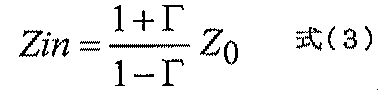
読出し位置決定部24は、テーブル選択部27によって選択された整合補正値テーブルを参照し、算出された入力インピーダンスZinに最も近いインピーダンス値を有する整合補正値テーブルの行から、使用すべき整合回路を示すフラグ情報If及び当該整合回路に適用すべき制御値Tcを読出す。そして、整合回路選択部23は、読出し位置決定部24から供給されるフラグ情報Ifに基づき、第1形式の整合回路11又は第2形式の整合回路12若しくは電線のみからなるスルー回路30のいずれかが送電回路2及び送電アンテナ3と電気的に接続されるようにスイッチ部13、14を制御する。制御値出力部26は、整合回路選択部23によって選択された第1形式の整合回路11又は第2形式の整合回路12に、読出し位置決定部24によって読出された制御値Tcを反映させる。
次に、記憶部25が記憶する整合補正量テーブルについて具体的に説明する。本実施例で使用する整合補正量テーブルは、図5、図6に示した送電アンテナ端での入力インピーダンスZinの変化の軌跡に基づいて設定することを特徴とする。なお図5は、負荷6の値をある値に固定した上で送電・受電アンテナ間の結合状態(即ち、結合係数k)を変化させた時の入力インピーダンスZinの軌跡を示している。一方、図6は、送電・受電アンテナ間の結合状態をある値に固定した上で受電側装置4の負荷6の値RLを変化させた時の入力インピーダンスZinの軌跡を示している。第1実施例では、負荷6の値RLは固定で送電アンテナ3及び受電アンテナ5間の結合状態を変化させた時の動作について説明しているので、以下では図5に示した軌跡を基にして整合補正量テーブルを構成する場合について説明する。
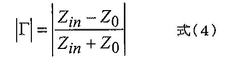
従って、入力インピーダンス軌跡上の各インピーダンスポイントZinを式(4)に従って反射係数絶対値|Γ|に変換し、その各々の値に対して、予め理論計算により求めたキャパシタンス値C、インダクタンス値Lの値の組を対応させた整合補正量テーブルを予め作成しておく。
以下では、自動整合動作の効果について例を挙げて説明する。
次に、第1実施例に係る整合追従動作について説明する。この動作は、一度インピーダンス整合を取った後に、整合状態を維持し続けるための動作である。
以下では、整合状態からのずれが、結合が強まる方向又は結合が弱まる方向のいずれの方向に生じているのかを判断する方法を説明する。この処理は、位相差算出・判定部16及び調整方向決定部18により実行される。
次に、反射係数絶対値|Γ|に基づきステップ幅Widxを決定する方法について説明する。
・「|Γ|の変化幅<0.15」の場合、「Widx=1」
・「|Γ|の変化幅<0.30」の場合、「Widx=2」
・「|Γ|の変化幅<0.45」の場合、「Widx=3」
・「|Γ|の変化幅≧0.45」の場合、「Widx=4」
このように、送電側装置1は、例えば、各反射係数絶対値|Γ|の変化幅に対応する適切なステップ幅Widxのテーブルを予め記憶部25に記憶しておく。上述のテーブルは、例えば実験等に基づき予め作成される。そして、送電側装置1は、反射係数絶対値|Γ|の変化幅から、このテーブルを参照してステップ幅Widxを決定することで、送電アンテナ3と受電アンテナ5との間の結合状態の変化が高速に起こるような場合にも迅速に整合状態を回復することができる。
次に、第1実施例における処理手順について説明する。以下では、まず、自動整合動作の処理手順について図26~図28の「フロー1」~「フロー3」で説明した後、追従整合動作の処理手順について図29の「フロー4」で説明する。
図26は、第1実施例において、送電側装置1が実行する処理手順を示すフローチャートである。送電側装置1は、図26のフロー1の処理を、所定のタイミングで実行する。
図27は、第1実施例において、受電側装置4の負荷推定部7が実行する処理手順を示すフローチャートである。負荷推定部7は、図27のフロー2の処理を、図26のステップS103で制御通信部75から負荷の値の推定を依頼する旨の信号を受信した場合に実行する。
図28は、第1実施例において、送電側装置1が実行するフロー3の処理手順を示すフローチャートである。送電側装置1は、図28のフロー3の処理を、図26のフロー1でステップS106へ処理を進めた際に実行する。
図29は、第1実施例において、送電側装置1が実行する処理手順を示すフローチャートである。送電側装置1は、図29のフロー4の処理を、フロー3の実行後に実行する。
次に、第2実施例について説明する。第2実施例では、結合係数kが変化せず、負荷6の値RLが変化する場合について説明する。概略的には、電力伝送システムは、結合係数k及び送電アンテナ端の入力インピーダンスZinを推定し、これらの推定値に基づき、整合補正量テーブルを参照して、使用すべき整合回路及び当該整合回路へ適用する制御値Tcを決定する。これにより、電力伝送システムは、送電アンテナの入力インピーダンスZinを、送電回路の出力インピーダンスと整合させる。また、電力伝送システムは、一度整合状態になった後に整合状態を維持し続ける整合追従動作を行うことで、整合状態を保つ。
図30は、第2実施例に係る電力伝送システムの概略構成図である。第2実施例では、負荷6の値RLが変化し、記憶部25は、結合係数kごとに負荷6の値RLが変化した場合の整合補正量テーブルを記憶する点で第1実施例と異なる。そして、送電側装置1は、初期状態から自動整合動作を行うと共に、自動整合動作後に整合追従動作を行う。以下では、第1実施例と同様の部分については適宜同一の符号を付し、その説明を省略する。
次に、第2実施例で記憶部25が予め記憶する整合補正量テーブルについて説明する。第1及び第2実施例で使用する整合補正量テーブルは、いずれも図5、図6に示した送電アンテナ端での入力インピーダンスZinの変化の軌跡に基づいて生成される。ここで、図6は、送電アンテナ3及び受電アンテナ5間の結合係数kを固定した上で負荷6の値RLを変化させた時の入力インピーダンス軌跡を示している。上述したように、第2実施例では、結合係数kを固定した上で受電側装置4の負荷6の値RLが変化するため、以下では図6に示したインピーダンス軌跡を基にして整合補正量テーブルを構成する場合について説明する。
以下では、自動整合動作の効果について例を挙げて説明する。
次に、第2実施例に係る整合追従動作について説明する。この動作は、一度インピーダンス整合を取った後に、整合状態を維持し続けるための動作である。
以下では、整合状態からのずれが、負荷が大きくなる方向又は負荷が小さくなる方向のいずれの方向に生じているのかを判断する方法を説明する。この処理は、位相差算出・判定部16及び調整方向決定部18により実行される。
次に、第2実施例における処理手順について説明する。以下では、まず、自動整合動作の処理手順について図41の「フロー5」及び図42の「フロー6」で説明した後、追従整合動作の処理手順について図43の「フロー7」で説明する。
図41は、第2実施例で送電側装置1が実行するフロー5の処理手順を示すフローチャートである。送電側装置1は、図41のフロー5の処理を、所定のタイミングで実行する。
図42は、第2実施例において、送電側装置1が実行するフロー6の処理手順を示すフローチャートである。送電側装置1は、図42のフロー6の処理を、図41のフロー5のステップS504へ処理を進めた際に実行する。
図43は、第2実施例において、送電側装置1が実行するフロー7の処理手順を示すフローチャートである。送電側装置1は、図43のフロー7の処理を、図42のフロー6の実行後直ちに実行する。
次に、第1実施例及び第2実施例に好適な変形例について説明する。以下に説明する変形例は、任意に組み合わせて、上述の第1実施例及び第2実施例に適用してもよい。
本発明に適用可能な整合回路の構成は、図12等に示す構成に限定されない。これについて、図44を参照して説明する。
図19及び図32等に示した整合補正量テーブルでは、制御値Tcとして、キャパシタンス値C及びインダクタンス値Lが記憶されているが、これに代えて、可変コンデンサ、可変インダクタの値を所定の値にするための制御値Tcが記憶されても良い.例えば、ステッピングモータとバリコンを組合せて可変コンデンサを構成したような場合ではモータの制御電圧値を整合補正量テーブルに記憶させてもよく、また、微小なコンデンサ、インダクタをリレー等のスイッチングデバイスでオン及びオフさせて所定のキャパシタンスC値及びリアクタンスL値を実現するような場合では、スイッチングデバイスを制御するためのビットパターン値を整合補正量テーブルに記憶させてもよい。
第1実施例の[整合補正量テーブル]のセクションの説明では、理論計算によって整合に必要な補正量A1、A2、B1、B2を求めたが、これに代えて、実際の送電アンテナ3及び受電アンテナ5を対向させ、それらの結合状態を変化させながらこれらの補正量A1、A2、B1、B2を求めても良い。
第1実施例では、定格電力の伝送に先立って、負荷推定部7は推定負荷値RLeを算出した。これに代えて、受電側装置4に存在する負荷6の値RLがシステムの仕様として予め決まっているような場合には、送電側装置1は、負荷推定部7により推定負荷値RLeを算出することなく、予めシステムで決められている負荷6の値に対応した整合補正量テーブルを選択する。
結合係数推定部8は、距離センサ81により送電アンテナ3と受電アンテナ5との距離を計測したがこれに限定されない。これに代えて、結合係数推定部8は、共振周波数を中心として所定の帯域幅の微小信号をスイープさせて送出し、送出した信号と送電アンテナ3から反射して戻ってきた信号とを用いて反射係数(ΓもしくはS11)の周波数特性を算出する。そして、結合係数推定部8は、算出した周波数特性の形状、具体的には、極小となるピークの個数とその周波数、及びその反射係数の大きさから所定のマップを参照して、結合係数推定値keを算出する。ここで、上述のマップは、反射係数の周波数特性において、極小となるピークの個数とその周波数、及びその反射係数の大きさに対応した結合係数kを示すマップであり、実験等に基づき予め作成され、メモリに予め記憶される。これによっても、好適に、結合係数推定部8は、結合係数kを推定することが可能となる。
送電アンテナ3及び受電アンテナ5は、直並列型等価回路によってモデル化された。これに代えて、送電アンテナ3及び受電アンテナ5は、直並列型等価回路をより簡略化した等価回路である直列共振等価回路によってモデル化されてもよい。
送電側装置1の整合回路選択部23は、記憶部25に記憶された整合補正量テーブルのフラグ情報Ifに基づき使用すべき整合回路を選択した。これに代えて、整合回路選択部23は、算出された入力インピーダンスZinに基づき、使用すべき整合回路を選択してもよい。
第1実施例及び第2実施例では、スイッチ部13、14で切換えられる回路の一つとして整合回路を挿入しないスルー回路30と記載したが、スルー回路30は、整合回路を挿入しないというスルーの状態と同様の効果を有する実装方法であれば、いかなる実装方法でも構わない。例えば、明示的に整合回路をスルーするような回路パスは持っていないが、可変インダクタンスの値をゼロとすることで整合回路が入っていない状態と等価にするような実装方法も、整合回路を挿入しないスルー回路30に切換えていることと同じであるものとする。
図12及び図30に示す送電側装置1の構成は一例であり、本発明が適用可能な構成は、これに限定されない。例えば、送電側装置1は、自動整合動作のみを行い、整合追従動作を行う必要がない場合には、調整方向決定部18及び調整ステップ幅決定部19を有しなくてもよい。
図12では、受電側装置4が負荷値算出部73により推定負荷値RLeの算出を行っているが、これに代えて、送電側装置1が推定負荷値RLeの算出を行ってもよい。この場合、受電側装置4は、負荷6の電圧値及び電流値を検出後、これらの値を制御通信部74を介して送電側装置1へ伝送し、送電側装置1は、伝送されたこれらの値に基づき推定負荷値RLeを算出する。
2 送電回路
3 送電アンテナ
4 受電側装置
5 受電アンテナ
6 負荷
7 負荷推定部
8 結合係数推定部
11 第1形式の整合回路
12 第2形式の整合回路
13、14 スイッチ部
15 進行波・反射波抽出部
16 位相差算出・判定部
17 反射係数算出部
18 調整方向決定部
19 調整ステップ幅決定部
23 整合回路選択部
24 読出し位置決定部
25 記憶部
26 制御値出力部
27 テーブル選択部
Claims (11)
- 送電アンテナと受電アンテナとを電磁界によって結合させて電力を伝送する無線電力伝送システムにおいて、送電回路と前記送電アンテナとの間に設置されるインピーダンス整合装置であって、
前記送電アンテナの入力インピーダンスもしくは当該入力インピーダンスに相当する入力インピーダンス相当値を推定する入力インピーダンス推定手段と、
前記送電回路と前記送電アンテナとの間に直列に挿入される可変インダクタ要素と、当該可変インダクタ要素よりも前記送電アンテナ側に並列に接続される可変キャパシタ要素と、を備える第1の整合回路と、
前記送電回路と前記送電アンテナとの間に直列に挿入される可変インダクタ要素と、当該可変インダクタ要素よりも前記送電回路側に並列に接続される可変キャパシタ要素と、を備える第2の整合回路と、
前記送電回路と前記送電アンテナとの間に直列に挿入されるスルー回路と、
前記受電アンテナに接続され前記伝送された電力が消費される回路の負荷の値を推定する負荷値推定手段と、
前記第1または前記第2の整合回路を用いて所定のインピーダンス値に整合させるために必要なインダクタンス値およびキャパシタンス値に対応した制御値を、前記負荷の値と前記入力インピーダンス相当値とに対応させて予め記憶する記憶部と、
前記負荷の値と前記入力インピーダンス相当値とに基づいて、前記第1の整合回路と前記第2の整合回路と前記スルー回路とのいずれか1つを電気的に接続する回路選択手段と、
前記負荷の値と前記入力インピーダンス相当値とに基づいて、前記記憶部に記憶された前記制御値を読出し、当該制御値を前記回路選択手段によって選択された回路に出力する制御値出力手段と、
を有することを特徴とするインピーダンス整合装置。 - 前記記憶部は、
前記制御値と、当該制御値を反映させる前記第1または前記第2の整合回路を示すフラグ情報とを、前記負荷の値と前記入力インピーダンス相当値とに対応させて予め記憶し、
前記回路選択手段は、
前記負荷の値と前記入力インピーダンス相当値とから決定される前記フラグ情報に基づいて、前記第1の整合回路と前記第2の整合回路とのいずれか1つを電気的に接続することを特徴とする請求項1に記載のインピーダンス整合装置。 - 前記制御値は、
前記回路の負荷の値を固定した上で、前記送電アンテナと前記受電アンテナとの間の結合状態を変更させた際の、前記送電回路から前記送電アンテナへの入力インピーダンスの変化の軌跡に基づいて設定されることを特徴とする請求項1または2に記載のインピーダンス整合装置。 - 送電アンテナと受電アンテナとを電磁界によって結合させて電力を伝送する無線電力伝送システムにおいて、送電回路と前記送電アンテナとの間に設置されるインピーダンス整合装置であって、
前記送電アンテナの入力インピーダンスもしくは当該入力インピーダンスに相当する入力インピーダンス相当値を推定する入力インピーダンス推定手段と、
前記送電回路と前記送電アンテナとの間に直列に挿入される可変インダクタ要素と、当該可変インダクタ要素よりも前記送電アンテナ側に並列に接続される可変キャパシタ要素と、を備える第1の整合回路と、
前記送電回路と前記送電アンテナとの間に直列に挿入される可変インダクタ要素と、当該可変インダクタ要素よりも前記送電回路側に並列に接続される可変キャパシタ要素と、を備える第2の整合回路と、
前記送電回路と前記送電アンテナとの間に直列に挿入されるスルー回路と、
前記送電アンテナと前記受電アンテナとの間の結合係数を推定する結合係数推定手段と、
前記第1または前記第2の整合回路を用いて所定のインピーダンス値に整合させるために必要なインダクタンス値およびキャパシタンス値に対応した制御値を、前記結合係数と前記入力インピーダンス相当値とに対応させて予め記憶する記憶部と、
前記結合係数と前記入力インピーダンス相当値とに基づいて、前記第1の整合回路と前記第2の整合回路と前記スルー回路とのいずれか1つを電気的に接続する回路選択手段と、
前記結合係数と前記入力インピーダンス相当値とに基づいて、前記記憶部に記憶された前記制御値を読出し、当該制御値を前記回路選択手段によって選択された回路に出力する制御値出力手段と、
を有することを特徴とするインピーダンス整合装置。 - 前記記憶部は、
前記制御値と、当該制御値を反映させる前記第1または前記第2の整合回路を示すフラグ情報とを、前記結合係数と前記入力インピーダンス相当値とに対応させて予め記憶し、
前記回路選択手段は、
前記結合係数と前記入力インピーダンス相当値とから決定される前記フラグ情報に基づいて、前記第1の整合回路と前記第2の整合回路とのいずれか1つを電気的に接続することを特徴とする請求項4に記載のインピーダンス整合装置。 - 前記制御値は、
前記送電アンテナと前記受電アンテナとの間の結合状態を固定した上で、前記回路の負荷の値を変更させた際の、前記送電回路から前記送電アンテナへの入力インピーダンスの変化の軌跡に基づいて設定されることを特徴とする請求項4または5に記載のインピーダンス整合装置。 - 前記送電回路からの出力信号に対応する進行波電圧と、前記送電アンテナからの反射信号に対応する反射波電圧と、を取り出す進行波・反射波抽出手段と、
前記進行波電圧と前記反射波電圧とに基づき、反射係数の絶対値または当該絶対値に対応する値である反射係数絶対値相当値を算出する反射係数算出手段と、
前記進行波電圧の位相と前記反射波電圧の位相とを比較し、当該位相間の位相差を算出する位相差算出手段と、
を更に有し、
前記入力インピーダンス推定手段は、前記入力インピーダンス相当値として前記反射係数絶対値相当値と前記位相差とを推定することを特徴とする請求項1乃至6のいずれか一項に記載のインピーダンス整合装置。 - 前記送電回路からの出力信号に対応する進行波電圧と、前記送電アンテナからの反射信号に対応する反射波電圧と、を取り出す進行波・反射波抽出手段と、
前記進行波電圧と前記反射波電圧とに基づき、反射係数の絶対値または当該絶対値に対応する値である反射係数絶対値相当値を算出する反射係数算出手段と、
前記回路選択手段は、前記反射係数絶対値相当値が所定値以下である場合は、前記スルー回路を選択することを特徴とする請求項1乃至7のいずれか一項に記載のインピーダンス整合装置。 - 前記制御値は、
反射係数の絶対値が大きくなるほど、量子化間隔が小さくなるように量子化されることを特徴とする請求項1乃至8のいずれか一項に記載のインピーダンス整合装置。 - 送電アンテナと受電アンテナとを電磁界によって結合させて電力を伝送する無線電力伝送システムにおいて、送電回路と前記送電アンテナとの間に設置され、
前記送電回路と前記送電アンテナとの間に直列に挿入される可変インダクタ要素と、当該可変インダクタ要素よりも前記送電アンテナ側に並列に接続される可変キャパシタ要素と、を備える第1の整合回路と、
前記送電回路と前記送電アンテナとの間に直列に挿入される可変インダクタ要素と、当該可変インダクタ要素よりも前記送電回路側に並列に接続される可変キャパシタ要素と、を備える第2の整合回路と、
前記送電回路と前記送電アンテナとの間に直列に挿入されるスルー回路と、
前記第1または前記第2の整合回路を用いて所定のインピーダンス値に整合させるために必要なインダクタンス値およびキャパシタンス値に対応した制御値を、前記受電アンテナに接続され前記伝送された電力が消費される回路の負荷の値と前記入力インピーダンス相当値とに対応させて予め記憶する記憶部と、を備えるインピーダンス整合装置が実行する制御方法であって、
前記送電アンテナの入力インピーダンスもしくは当該入力インピーダンスに相当する入力インピーダンス相当値を推定する入力インピーダンス推定工程と、
前記負荷の値を推定する負荷値推定工程と、
前記負荷の値と前記入力インピーダンス相当値とに基づいて、前記第1の整合回路と前記第2の整合回路と前記スルー回路とのいずれか1つを電気的に接続する回路選択工程と、
前記負荷の値と前記入力インピーダンス相当値とに基づいて、前記記憶部に記憶された前記制御値を読出し、当該制御値を前記回路選択工程によって選択された回路に出力する制御値出力工程と、
を有することを特徴とする制御方法。 - 送電アンテナと受電アンテナとを電磁界によって結合させて電力を伝送する無線電力伝送システムにおいて、送電回路と前記送電アンテナとの間に設置され、
前記送電回路と前記送電アンテナとの間に直列に挿入される可変インダクタ要素と、当該可変インダクタ要素よりも前記送電アンテナ側に並列に接続される可変キャパシタ要素と、を備える第1の整合回路と、
前記送電回路と前記送電アンテナとの間に直列に挿入される可変インダクタ要素と、当該可変インダクタ要素よりも前記送電回路側に並列に接続される可変キャパシタ要素と、を備える第2の整合回路と、
前記送電回路と前記送電アンテナとの間に直列に挿入されるスルー回路と、
前記第1または前記第2の整合回路を用いて所定のインピーダンス値に整合させるために必要なインダクタンス値およびキャパシタンス値に対応した制御値を、前記送電アンテナと前記受電アンテナとの間の結合係数と前記入力インピーダンス相当値とに対応させて予め記憶する記憶部と、を備えるインピーダンス整合装置が実行する制御方法であって、
前記送電アンテナの入力インピーダンスもしくは当該入力インピーダンスに相当する入力インピーダンス相当値を推定する入力インピーダンス推定工程と、
前記結合係数を推定する結合状態推定工程と、
前記結合係数と前記入力インピーダンス相当値とに基づいて、前記第1の整合回路と前記第2の整合回路と前記スルー回路とのいずれか1つを電気的に接続する回路選択工程と、
前記結合係数と前記入力インピーダンス相当値とに基づいて、前記記憶部に記憶された前記制御値を読出し、当該制御値を前記回路選択工程によって選択された回路に出力する制御値出力工程と、
を有することを特徴とする制御方法。
Priority Applications (6)
| Application Number | Priority Date | Filing Date | Title |
|---|---|---|---|
| US14/124,359 US9331663B2 (en) | 2011-06-07 | 2011-06-07 | Impedance matching device and control method |
| PCT/JP2011/063069 WO2012169014A1 (ja) | 2011-06-07 | 2011-06-07 | インピーダンス整合装置、制御方法 |
| JP2013519264A JP5712289B2 (ja) | 2011-06-07 | 2011-06-07 | インピーダンス整合装置、制御方法 |
| JP2015046222A JP5957556B2 (ja) | 2011-06-07 | 2015-03-09 | インピーダンス整合装置、受電側装置、及び制御方法 |
| US14/692,765 US9337798B2 (en) | 2011-06-07 | 2015-04-22 | Impedance matching device, power reception-side device, and control method |
| US14/692,790 US9276553B2 (en) | 2011-06-07 | 2015-04-22 | Impedance matching device and control method |
Applications Claiming Priority (2)
| Application Number | Priority Date | Filing Date | Title |
|---|---|---|---|
| PCT/JP2011/063069 WO2012169014A1 (ja) | 2011-06-07 | 2011-06-07 | インピーダンス整合装置、制御方法 |
| JP2015046222A JP5957556B2 (ja) | 2011-06-07 | 2015-03-09 | インピーダンス整合装置、受電側装置、及び制御方法 |
Related Child Applications (3)
| Application Number | Title | Priority Date | Filing Date |
|---|---|---|---|
| US14/124,359 A-371-Of-International US9331663B2 (en) | 2011-06-07 | 2011-06-07 | Impedance matching device and control method |
| US14/692,765 Division US9337798B2 (en) | 2003-09-23 | 2015-04-22 | Impedance matching device, power reception-side device, and control method |
| US14/692,790 Division US9276553B2 (en) | 2011-06-07 | 2015-04-22 | Impedance matching device and control method |
Publications (1)
| Publication Number | Publication Date |
|---|---|
| WO2012169014A1 true WO2012169014A1 (ja) | 2012-12-13 |
Family
ID=55709588
Family Applications (1)
| Application Number | Title | Priority Date | Filing Date |
|---|---|---|---|
| PCT/JP2011/063069 Ceased WO2012169014A1 (ja) | 2011-06-07 | 2011-06-07 | インピーダンス整合装置、制御方法 |
Country Status (3)
| Country | Link |
|---|---|
| US (3) | US9331663B2 (ja) |
| JP (2) | JP5712289B2 (ja) |
| WO (1) | WO2012169014A1 (ja) |
Cited By (7)
| Publication number | Priority date | Publication date | Assignee | Title |
|---|---|---|---|---|
| WO2013125526A1 (ja) * | 2012-02-21 | 2013-08-29 | 株式会社 豊田自動織機 | 非接触電力伝送装置 |
| WO2014136257A1 (ja) * | 2013-03-08 | 2014-09-12 | パイオニア株式会社 | 受電装置 |
| JP2014175595A (ja) * | 2013-03-12 | 2014-09-22 | Saitama Univ | 磁気浮上装置 |
| WO2015122292A1 (ja) * | 2014-02-13 | 2015-08-20 | 株式会社 豊田自動織機 | 送電機器及び非接触電力伝送装置 |
| EP2993677A4 (en) * | 2013-04-16 | 2017-01-11 | Nitto Denko Corporation | Wireless power transmission device, heat generation control method for wireless power transmission device, and production method for wireless power transmission device |
| JP2018107910A (ja) * | 2016-12-27 | 2018-07-05 | 昭和飛行機工業株式会社 | 非接触給電装置 |
| CN110679060A (zh) * | 2017-05-30 | 2020-01-10 | 通用电气公司 | 用于通用无线充电装置的传输组件及其方法 |
Families Citing this family (41)
| Publication number | Priority date | Publication date | Assignee | Title |
|---|---|---|---|---|
| JP5749208B2 (ja) * | 2012-03-26 | 2015-07-15 | 株式会社東芝 | 送電装置、受電装置、制御装置および無線電力伝送システム |
| US20130257667A1 (en) * | 2012-03-30 | 2013-10-03 | Broadcom Corporation | Antenna Tuning |
| US10291067B2 (en) | 2012-07-27 | 2019-05-14 | Tc1 Llc | Computer modeling for resonant power transfer systems |
| US9592397B2 (en) | 2012-07-27 | 2017-03-14 | Thoratec Corporation | Thermal management for implantable wireless power transfer systems |
| WO2014018973A1 (en) | 2012-07-27 | 2014-01-30 | Thoratec Corporation | Resonant power transmission coils and systems |
| US9805863B2 (en) | 2012-07-27 | 2017-10-31 | Thoratec Corporation | Magnetic power transmission utilizing phased transmitter coil arrays and phased receiver coil arrays |
| US10525181B2 (en) | 2012-07-27 | 2020-01-07 | Tc1 Llc | Resonant power transfer system and method of estimating system state |
| WO2014018967A1 (en) | 2012-07-27 | 2014-01-30 | Thoratec Corporation | Self-tuning resonant power transfer systems |
| US10383990B2 (en) | 2012-07-27 | 2019-08-20 | Tc1 Llc | Variable capacitor for resonant power transfer systems |
| WO2014018971A1 (en) | 2012-07-27 | 2014-01-30 | Thoratec Corporation | Resonant power transfer systems with protective algorithm |
| EP2878060A4 (en) * | 2012-07-27 | 2016-04-06 | Thoratec Corp | WIRELESS BATTERY CHARGING |
| JP6119756B2 (ja) * | 2012-09-13 | 2017-04-26 | トヨタ自動車株式会社 | 非接触給電システムおよび送電装置 |
| KR102123829B1 (ko) * | 2013-01-22 | 2020-06-18 | 삼성전자주식회사 | 무선 전력 전송 장치 및 무선 전력 전송 방법 |
| US10373756B2 (en) | 2013-03-15 | 2019-08-06 | Tc1 Llc | Malleable TETs coil with improved anatomical fit |
| WO2014145664A1 (en) | 2013-03-15 | 2014-09-18 | Thoratec Corporation | Integrated implantable tets housing including fins and coil loops |
| JP6108915B2 (ja) * | 2013-04-02 | 2017-04-05 | キヤノン株式会社 | 受電装置、その制御方法およびプログラム |
| US9621129B2 (en) * | 2013-06-28 | 2017-04-11 | Skyworks Solutions, Inc. | Flexible L-network antenna tuner circuit |
| EP3069358B1 (en) | 2013-11-11 | 2019-06-12 | Tc1 Llc | Hinged resonant power transfer coil |
| WO2015070200A1 (en) | 2013-11-11 | 2015-05-14 | Thoratec Corporation | Resonant power transfer systems with communications |
| EP3072210B1 (en) | 2013-11-11 | 2023-12-20 | Tc1 Llc | Resonant power transfer systems with communications |
| WO2015097804A1 (ja) * | 2013-12-26 | 2015-07-02 | 三菱電機エンジニアリング株式会社 | 高周波電源用自動整合回路 |
| WO2015134871A1 (en) | 2014-03-06 | 2015-09-11 | Thoratec Corporation | Electrical connectors for implantable devices |
| EP3826104B1 (en) | 2014-09-22 | 2023-05-03 | Tc1 Llc | Antenna designs for communication between a wirelessly powered implant to an external device outside the body |
| EP3204989B1 (en) | 2014-10-06 | 2019-08-21 | Tc1 Llc | Multiaxial connector for implantable devices |
| US10148126B2 (en) | 2015-08-31 | 2018-12-04 | Tc1 Llc | Wireless energy transfer system and wearables |
| EP3902100A1 (en) | 2015-10-07 | 2021-10-27 | Tc1 Llc | Resonant power transfer systems having efficiency optimization based on receiver impedance |
| KR102572577B1 (ko) * | 2016-04-15 | 2023-08-30 | 삼성전자주식회사 | 무선 충전을 제어하는 충전 장치 및 방법 |
| JP6675093B2 (ja) * | 2016-05-31 | 2020-04-01 | パナソニックIpマネジメント株式会社 | 非接触給電装置、プログラム、非接触給電装置の制御方法、及び非接触電力伝送システム |
| EP3476043A4 (en) * | 2016-06-26 | 2020-07-22 | The Regents of The University of Colorado, A Body Corporate | ADAPTATION NETWORKS FOR WIRELESS POWER TRANSFER AND ASSOCIATED TECHNIQUES |
| US10898292B2 (en) | 2016-09-21 | 2021-01-26 | Tc1 Llc | Systems and methods for locating implanted wireless power transmission devices |
| WO2018136592A2 (en) | 2017-01-18 | 2018-07-26 | Tc1 Llc | Systems and methods for transcutaneous power transfer using microneedles |
| US10560953B2 (en) | 2017-02-20 | 2020-02-11 | Samsung Electronics Co., Ltd. | Antenna tuning devices and antenna tuning methods |
| WO2018212074A1 (ja) * | 2017-05-19 | 2018-11-22 | オムロン株式会社 | 非接触給電装置 |
| KR102061936B1 (ko) | 2017-08-24 | 2020-01-02 | 한국과학기술원 | 피드백을 통해 에너지 충전 효율을 높이기 위해 두 가지 충전모드를 제공하는 무선 전력 시스템 및 방법 |
| WO2019135890A1 (en) | 2018-01-04 | 2019-07-11 | Tc1 Llc | Systems and methods for elastic wireless power transmission devices |
| JP7003708B2 (ja) * | 2018-02-07 | 2022-01-21 | オムロン株式会社 | 非接触給電装置 |
| JP7278136B2 (ja) * | 2019-04-08 | 2023-05-19 | 東京エレクトロン株式会社 | インピーダンス整合装置、異常診断方法及び異常診断プログラム |
| JP7286389B2 (ja) * | 2019-04-15 | 2023-06-05 | キヤノン株式会社 | 無線通信装置、無線通信システムおよび通信方法 |
| WO2021014932A1 (ja) * | 2019-07-25 | 2021-01-28 | 株式会社デンソー | 非接触給電装置 |
| KR102896241B1 (ko) * | 2021-03-31 | 2025-12-08 | 삼성전자주식회사 | 무선 전력 수신, 무선 통신, 및 전기 자극을 수행하는 장치 및 방법 |
| WO2023157431A1 (ja) * | 2022-02-16 | 2023-08-24 | パナソニックIpマネジメント株式会社 | 高周波処理装置 |
Citations (6)
| Publication number | Priority date | Publication date | Assignee | Title |
|---|---|---|---|---|
| JPH07273680A (ja) * | 1994-03-31 | 1995-10-20 | Icom Inc | オートアンテナチューナーの制御方法 |
| JP2005129985A (ja) * | 2003-10-21 | 2005-05-19 | Hitachi Kokusai Electric Inc | 自動インピーダンス整合方法 |
| JP2010130800A (ja) * | 2008-11-28 | 2010-06-10 | Nagano Japan Radio Co | 非接触型電力伝送システム |
| WO2010067763A1 (ja) * | 2008-12-09 | 2010-06-17 | 株式会社 豊田自動織機 | 非接触電力伝送装置及び非接触電力伝送装置における電力伝送方法 |
| JP2011010435A (ja) * | 2009-06-25 | 2011-01-13 | Fujitsu Ten Ltd | 非接触式電力供給装置および非接触式電力供給ユニット |
| JP2011050140A (ja) * | 2009-08-26 | 2011-03-10 | Sony Corp | 非接触給電装置、非接触受電装置、非接触給電方法、非接触受電方法および非接触給電システム |
Family Cites Families (7)
| Publication number | Priority date | Publication date | Assignee | Title |
|---|---|---|---|---|
| JPH04225953A (ja) | 1990-05-07 | 1992-08-14 | Shionogi & Co Ltd | スピロ ジベンゾスベラン誘導体 |
| US5589844A (en) * | 1995-06-06 | 1996-12-31 | Flash Comm, Inc. | Automatic antenna tuner for low-cost mobile radio |
| JP2004088701A (ja) * | 2002-08-29 | 2004-03-18 | Daihen Corp | インピーダンス自動整合装置 |
| KR100565284B1 (ko) | 2003-07-30 | 2006-03-30 | 엘지전자 주식회사 | 이동통신단말기의 송신장치 |
| EP1845627A4 (en) * | 2005-01-31 | 2014-07-30 | Panasonic Corp | ADAPTIVE IMPEDANCE ADAPTABLE MOBILE RADIO DEVICE |
| KR101118710B1 (ko) | 2005-07-12 | 2012-03-13 | 메사추세츠 인스티튜트 오브 테크놀로지 | 무선 비-방사성 에너지 전달 |
| JP5114371B2 (ja) | 2008-12-09 | 2013-01-09 | 株式会社豊田自動織機 | 非接触電力伝送装置 |
-
2011
- 2011-06-07 JP JP2013519264A patent/JP5712289B2/ja active Active
- 2011-06-07 US US14/124,359 patent/US9331663B2/en active Active
- 2011-06-07 WO PCT/JP2011/063069 patent/WO2012169014A1/ja not_active Ceased
-
2015
- 2015-03-09 JP JP2015046222A patent/JP5957556B2/ja active Active
- 2015-04-22 US US14/692,765 patent/US9337798B2/en active Active
- 2015-04-22 US US14/692,790 patent/US9276553B2/en active Active
Patent Citations (6)
| Publication number | Priority date | Publication date | Assignee | Title |
|---|---|---|---|---|
| JPH07273680A (ja) * | 1994-03-31 | 1995-10-20 | Icom Inc | オートアンテナチューナーの制御方法 |
| JP2005129985A (ja) * | 2003-10-21 | 2005-05-19 | Hitachi Kokusai Electric Inc | 自動インピーダンス整合方法 |
| JP2010130800A (ja) * | 2008-11-28 | 2010-06-10 | Nagano Japan Radio Co | 非接触型電力伝送システム |
| WO2010067763A1 (ja) * | 2008-12-09 | 2010-06-17 | 株式会社 豊田自動織機 | 非接触電力伝送装置及び非接触電力伝送装置における電力伝送方法 |
| JP2011010435A (ja) * | 2009-06-25 | 2011-01-13 | Fujitsu Ten Ltd | 非接触式電力供給装置および非接触式電力供給ユニット |
| JP2011050140A (ja) * | 2009-08-26 | 2011-03-10 | Sony Corp | 非接触給電装置、非接触受電装置、非接触給電方法、非接触受電方法および非接触給電システム |
Cited By (13)
| Publication number | Priority date | Publication date | Assignee | Title |
|---|---|---|---|---|
| WO2013125526A1 (ja) * | 2012-02-21 | 2013-08-29 | 株式会社 豊田自動織機 | 非接触電力伝送装置 |
| JP2013172560A (ja) * | 2012-02-21 | 2013-09-02 | Toyota Industries Corp | 非接触電力伝送装置 |
| US9577465B2 (en) | 2012-02-21 | 2017-02-21 | Kabushiki Kaisha Toyota Jidoshokki | Contactless power transmission device |
| WO2014136257A1 (ja) * | 2013-03-08 | 2014-09-12 | パイオニア株式会社 | 受電装置 |
| JPWO2014136257A1 (ja) * | 2013-03-08 | 2017-02-09 | パイオニア株式会社 | 受電装置 |
| JP2014175595A (ja) * | 2013-03-12 | 2014-09-22 | Saitama Univ | 磁気浮上装置 |
| EP2993677A4 (en) * | 2013-04-16 | 2017-01-11 | Nitto Denko Corporation | Wireless power transmission device, heat generation control method for wireless power transmission device, and production method for wireless power transmission device |
| JP2015154553A (ja) * | 2014-02-13 | 2015-08-24 | 株式会社豊田自動織機 | 送電機器及び非接触電力伝送装置 |
| WO2015122292A1 (ja) * | 2014-02-13 | 2015-08-20 | 株式会社 豊田自動織機 | 送電機器及び非接触電力伝送装置 |
| EP3107189A4 (en) * | 2014-02-13 | 2017-03-29 | Kabushiki Kaisha Toyota Jidoshokki | Power transmission equipment and non-contact power transmission device |
| JP2018107910A (ja) * | 2016-12-27 | 2018-07-05 | 昭和飛行機工業株式会社 | 非接触給電装置 |
| CN110679060A (zh) * | 2017-05-30 | 2020-01-10 | 通用电气公司 | 用于通用无线充电装置的传输组件及其方法 |
| CN110679060B (zh) * | 2017-05-30 | 2024-05-24 | 通用电气公司 | 用于通用无线充电装置的传输组件及其方法 |
Also Published As
| Publication number | Publication date |
|---|---|
| US9337798B2 (en) | 2016-05-10 |
| US20140191819A1 (en) | 2014-07-10 |
| US20150229289A1 (en) | 2015-08-13 |
| JP5957556B2 (ja) | 2016-07-27 |
| JP5712289B2 (ja) | 2015-05-07 |
| US20150229137A1 (en) | 2015-08-13 |
| US9276553B2 (en) | 2016-03-01 |
| JPWO2012169014A1 (ja) | 2015-02-23 |
| JP2015122955A (ja) | 2015-07-02 |
| US9331663B2 (en) | 2016-05-03 |
Similar Documents
| Publication | Publication Date | Title |
|---|---|---|
| JP5957556B2 (ja) | インピーダンス整合装置、受電側装置、及び制御方法 | |
| JP5710759B2 (ja) | インピーダンス整合装置、制御方法 | |
| JP5559665B2 (ja) | 非接触給電装置のインピーダンス整合方法とそれを用いた非接触給電装置 | |
| US11303325B2 (en) | Electric power transmitting device, non-contact power supply system, and control method | |
| JP4856288B1 (ja) | インピーダンス整合装置、制御方法 | |
| JP6417992B2 (ja) | 非接触給電システム | |
| JP5569182B2 (ja) | 非接触送電システム、非接触送電装置、およびインピーダンスの調整方法 | |
| US9362983B2 (en) | Method and apparatus for controlling resonance bandwidth in a wireless power transmission system | |
| Kim et al. | Coupling extraction and maximum efficiency tracking for multiple concurrent transmitters in dynamic wireless charging | |
| JP5544386B2 (ja) | インピーダンス整合装置、制御方法 | |
| US9178388B2 (en) | Wireless power transmission apparatus | |
| US20160226312A1 (en) | Wireless power reception system, wireless power transmission system, control method, computer program, and recording medium | |
| WO2013183700A1 (ja) | 受電機器及び非接触電力伝送装置 | |
| JP5819502B2 (ja) | インピーダンス整合装置及び制御方法 | |
| JP5059243B2 (ja) | インピーダンス整合装置、制御方法 | |
| JPWO2014030690A1 (ja) | 非接触電力伝送装置 | |
| CN117254604A (zh) | 基于连续域束缚态的无线电能传输系统及方法 | |
| CN121216754A (zh) | 一种阵列式无线电能传输系统的效率优化方法 |
Legal Events
| Date | Code | Title | Description |
|---|---|---|---|
| 121 | Ep: the epo has been informed by wipo that ep was designated in this application |
Ref document number: 11867375 Country of ref document: EP Kind code of ref document: A1 |
|
| ENP | Entry into the national phase |
Ref document number: 2013519264 Country of ref document: JP Kind code of ref document: A |
|
| NENP | Non-entry into the national phase |
Ref country code: DE |
|
| WWE | Wipo information: entry into national phase |
Ref document number: 14124359 Country of ref document: US |
|
| 122 | Ep: pct application non-entry in european phase |
Ref document number: 11867375 Country of ref document: EP Kind code of ref document: A1 |