WO2012168980A1 - 画像表示装置 - Google Patents
画像表示装置 Download PDFInfo
- Publication number
- WO2012168980A1 WO2012168980A1 PCT/JP2011/003284 JP2011003284W WO2012168980A1 WO 2012168980 A1 WO2012168980 A1 WO 2012168980A1 JP 2011003284 W JP2011003284 W JP 2011003284W WO 2012168980 A1 WO2012168980 A1 WO 2012168980A1
- Authority
- WO
- WIPO (PCT)
- Prior art keywords
- free
- form surface
- image display
- mirror
- display device
- Prior art date
- Legal status (The legal status is an assumption and is not a legal conclusion. Google has not performed a legal analysis and makes no representation as to the accuracy of the status listed.)
- Ceased
Links
Images












Classifications
-
- G—PHYSICS
- G02—OPTICS
- G02B—OPTICAL ELEMENTS, SYSTEMS OR APPARATUS
- G02B26/00—Optical devices or arrangements for the control of light using movable or deformable optical elements
- G02B26/08—Optical devices or arrangements for the control of light using movable or deformable optical elements for controlling the direction of light
- G02B26/10—Scanning systems
-
- G—PHYSICS
- G02—OPTICS
- G02B—OPTICAL ELEMENTS, SYSTEMS OR APPARATUS
- G02B17/00—Systems with reflecting surfaces, with or without refracting elements
- G02B17/08—Catadioptric systems
-
- G—PHYSICS
- G02—OPTICS
- G02B—OPTICAL ELEMENTS, SYSTEMS OR APPARATUS
- G02B13/00—Optical objectives specially designed for the purposes specified below
- G02B13/16—Optical objectives specially designed for the purposes specified below for use in conjunction with image converters or intensifiers, or for use with projectors, e.g. objectives for projection TV
-
- G—PHYSICS
- G02—OPTICS
- G02B—OPTICAL ELEMENTS, SYSTEMS OR APPARATUS
- G02B17/00—Systems with reflecting surfaces, with or without refracting elements
- G02B17/08—Catadioptric systems
- G02B17/0852—Catadioptric systems having a field corrector only
-
- G—PHYSICS
- G02—OPTICS
- G02B—OPTICAL ELEMENTS, SYSTEMS OR APPARATUS
- G02B26/00—Optical devices or arrangements for the control of light using movable or deformable optical elements
- G02B26/08—Optical devices or arrangements for the control of light using movable or deformable optical elements for controlling the direction of light
- G02B26/10—Scanning systems
- G02B26/101—Scanning systems with both horizontal and vertical deflecting means, e.g. raster or XY scanners
-
- H—ELECTRICITY
- H04—ELECTRIC COMMUNICATION TECHNIQUE
- H04N—PICTORIAL COMMUNICATION, e.g. TELEVISION
- H04N9/00—Details of colour television systems
- H04N9/12—Picture reproducers
- H04N9/31—Projection devices for colour picture display, e.g. using electronic spatial light modulators [ESLM]
- H04N9/3129—Projection devices for colour picture display, e.g. using electronic spatial light modulators [ESLM] scanning a light beam on the display screen
Definitions
- the present invention relates to an image display device.
- Patent Document 1 there is a problem that the movement locus of the scanning coordinates on the image plane is sinusoidal and has poor linearity. Further, according to Patent Document 2, there is a problem that the distance between the front and rear of the mirror needs to be increased, and the entire optical system is increased in size.
- an object of the present invention is to provide an image display device having scanning characteristics with excellent linearity without increasing the size of the device.
- the image display device includes: an optical scanning unit that scans light emitted from a light source in a first direction and a second direction of an image plane by reciprocating rotational movement of a reflection surface of the light; and An optical system that expands the scanning angle is provided.
- the optical system includes a free-form surface lens on the optical scanning unit side and a free-form surface mirror on the image surface side.
- FIG. 3 is a diagram illustrating lens data of Example 1.
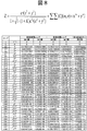
- FIG. 3 is a diagram illustrating a mathematical expression and specific values of a free-form surface coefficient according to the first embodiment.
- FIG. 3 is a distortion performance diagram of Example 1.
- FIG. 3 is a diagram illustrating a relationship between a light incident angle and a phase on an image plane according to the first exemplary embodiment.
- FIG. 3 is a diagram illustrating a relationship between a light incident coordinate and a phase on an image plane according to the first exemplary embodiment.
- FIG. 6 is a ray diagram of Example 2.
- FIG. 6 is another ray diagram of the second embodiment.
- FIG. 5 is a detailed diagram of a free-form surface lens of Example 2.
- FIG. 6 is a diagram showing lens data of Example 2.
- FIG. 10 is a diagram illustrating specific values of free-form surface coefficients according to the second embodiment.
- FIG. 6 is a ray diagram of Example 3.
- FIG. 6 is another ray diagram of the third embodiment.
- FIG. 5 is a detailed view of a free-form surface lens of Example 3.
- FIG. 6 is a diagram showing lens data of Example 3.
- FIG. 10 is a diagram illustrating specific values of free-form surface coefficients according to the third embodiment.
- FIG. 6 is a distortion performance diagram of Example 3.
- FIG. 6 is a relationship diagram between a conventional rotation angle and a scanning position.
- the change figure of the swing angle by the conventional phase The figure which shows the relationship between the incident angle of the light ray in the conventional image surface, and a phase.
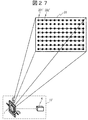
- FIG. 27 is a system diagram including a conventional image display device.
- the optical scanning unit 1 of the image display device 10 ′ scans the laser beam from the light source 4 on the image plane (screen) 20 while reflecting the laser beam with a reflection mirror having a rotation axis.
- Each pixel 201 ' is scanned two-dimensionally along the scanning trajectory 202'.
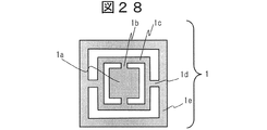
- FIG. 28 is an enlarged view of the optical scanning unit.
- the optical scanning unit 1 is connected to a mirror 1a for deflecting laser light at a reflection angle, a first torsion spring 1b connected to the mirror 1a, a holding member 1c connected to the first torsion spring 1b, and a holding member 1c.
- a second torsion spring 1d, and a permanent magnet and a coil (not shown).
- the coil is formed substantially parallel to the mirror 1a, and when the mirror 1a is stationary, a magnetic field substantially parallel to the mirror 1a is generated.
- a Lorentz force substantially perpendicular to the mirror 1a is generated according to Fleming's left-hand rule.
- Mirror 1a rotates to a position where Lorentz force and restoring force of torsion springs 1b and 1d are balanced.
- the mirror 1a By supplying an alternating current to the coil at the resonance frequency of the mirror 1a, the mirror 1a performs a resonance operation and the torsion spring 1b rotates.
- the torsion spring 1b rotates.
- the torsion spring 1d rotates. In this way, resonant operations with different resonant frequencies are realized in the two directions.
- a sinusoidal drive may be applied although it is not the resonance operation.
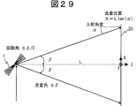
- FIG. 29 is a diagram showing the relationship between the conventional rotation angle and the scanning position. If the rotation angle of the optical scanning unit 1 is ⁇ / 2, the scanning angle that is the angle of the reflected light beam is ⁇ . Here, when no optical element is disposed between the optical scanning unit 1 and the image plane 20, the scanning angle ⁇ is equal to the incident angle ⁇ on the image plane 20. Therefore, the size of the scanned image for a certain projection distance is determined by the rotation angle ⁇ / 2.
- FIG. 30 is a change diagram of the swing angle of the conventional mirror surface.
- the swing angle ⁇ changes sinusoidally within a range of ⁇ ⁇ / 2.
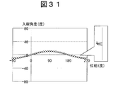
- FIG. 31 is a diagram showing the relationship between the incident angle and phase of the light beam on the conventional image plane
- FIG. 32 is a diagram showing the relationship between the incident coordinate and phase of the light beam on the conventional image surface.
- FIG. 32 has a sine wave shape similar to FIG.
- the optical scanning unit 1 with a rotation angle of ⁇ 5.3 degrees is used. That is, the scanning angle is ⁇ 10.6 degrees, and the incident angle on the image plane is also ⁇ 10.6 degrees.
- the driving method of the optical scanning unit 1 includes a galvano mirror that has a sawtooth wave-like rotation angle change in addition to a resonant mirror that has a sinusoidal wave-like rotation angle change.
- a resonance type mirror having a high driving frequency is suitable.
- scanning for one pixel in the vertical direction is performed in the horizontal direction while scanning for one reciprocation in the vertical direction is performed.
- scanning for one scanning line is performed.
- the display resolution number of pixels
- the optical scanning unit 1 rotates in a sinusoidal manner, the angle change of the mirror 1a appears periodically, although it is fast and slow.
- the change in the scan position on the image plane also becomes fast, and when the angle change is slow, the scan position on the image plane. Changes will also be slow. Therefore, light and dark corresponding to a sine wave is generated on the image plane.
- the circuit processing that thins out the laser beam in a bright portion with a dense pixel distribution and a sinusoidal wave shape can be improved if it is only bright and dark on the image plane, the linearity of the two-dimensional image cannot be improved, and the circuit scale increases. However, the amount of light decreases. If the laser beam is modulated in accordance with the timing of pixel arrangement on the image plane, the linearity can be improved, but the circuit scale increases more and more.
- a method using a plurality of reflecting surfaces can be considered in addition to the mirror, but if there is a shape error or decentration / falling of the optical component in manufacturing, the variation in the light beam angle at the mirror compared to the lens surface that is the transmission surface Is approximately doubled, making it difficult to manufacture an optical system using many mirrors. Furthermore, in an optical system using a plurality of mirrors, in order to secure an optical path before and after the reflection of laser light by the mirror, it is necessary to increase the distance before and after the mirror, and the entire optical system is increased in size.
- FIG. 1 is a system diagram including an image display device.
- the direction from the left to the right of the paper surface is defined as the X direction
- the direction from the bottom to the top of the image surface 20 is defined as the Y direction
- the direction from the front to the back of the paper surface is defined as the Z direction.
- 2, 27, and 29 also use the same coordinate system as FIG.
- a local coordinate system with the optical axis as the Z direction is handled.
- the system includes an image display device 10, a structure 30 that holds the image display device 10, and an image plane 20.
- the image display device 10 includes a light source 4, a light scanning unit 1 that deflects laser light from the light source 4 two-dimensionally, a free-form curved lens 2 that transmits and refracts the laser light deflected by the light scanning unit 1, and
- the free-form surface mirror 3 reflects the laser light from the free-form surface lens 2 and guides it to the image plane 20. With these optical components, a two-dimensional scanning image having a rectangular and uniform light quantity distribution is displayed on the image plane 20 under the effect of improving the linearity and widening the angle (described later).
- the optical scanning unit 1 may realize scanning in the long side direction and the short side direction with a single reflecting surface (mirror 1a), or may have each reflecting surface according to each direction. Good.
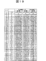
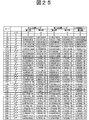
- a shape which is rotationally asymmetric and has parameters as shown in FIGS. 8, 19 and 25 is called a free-form surface.
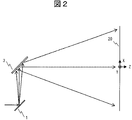
- FIG. 2 is a view of the system of FIG. 1 as viewed from above.
- the side corresponding to the X direction in the image plane 20 is longer than the side corresponding to the Y direction, the former is called a long side and the latter is called a short side. Further, the larger direction of the deflection angle of the reflecting surface corresponds to the long side direction, and the small direction corresponds to the short side direction.
- the long side is substantially parallel to the first plane (XZ plane) defined by the incident ray and the reflected ray in the free-form surface mirror 3.
- a free-form surface mirror 3 is arranged. This is because the free-form surface mirror 3 is arranged obliquely with respect to the long-side light beam having a large scanning amount, so that the light beam scanned at a scan angle that is twice a predetermined rotation angle can be obtained. This is because the range of coordinates reflected by is increased, and the degree of freedom of shape of the free-form mirror 3 is increased.
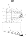
- FIG. 3 is a ray diagram showing how the light beam emitted from the image display device 10 reaches a 5 ⁇ 5 division point on the image plane 20.
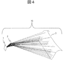
- FIG. 4 is another ray diagram, in which the laser beam emitted from the light source 4 is deflected by the rotation of the optical scanning unit 1 and then reaches the image plane 20 via the free-form surface lens 2 and the free-form surface mirror 3. Show. Further, FIG. 5 is a detailed view of the free-form surface lens 2, which is composed of a first free-form surface lens 2a and a second free-form surface lens 2b.
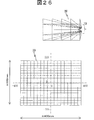
- FIG. 6 is a three-dimensional ray diagram.
- FIG. 3 since it is difficult to understand that the light beam reflected by the free-form surface mirror 3 does not irradiate the free-form surface lens 2 again, FIG. 6 shows that optical path interference does not occur.
- FIG. 7 shows a MEMS (Micro-Electro-Mechanical System) mirror (resonance rotation of horizontal ⁇ 5.3 degrees, vertical ⁇ 2.9 degrees), a free-form surface lens, and a free-form lens as light scanning unit 1 from light source 4 that is the 0th surface
- FIG. 8 is a diagram showing lens data of a curved mirror
- FIG. 8 is a diagram showing formulas and specific values of free-form surface coefficients of the free-form surface.
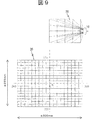
- FIG. 9 is a distortion performance diagram.
- light beams having a scanning angle of the optical scanning unit 1 having a rotation angle of ⁇ 5.3 degrees in the long side direction (main scanning direction) and a rotation angle of ⁇ 2.9 degrees in the short side direction (sub-scanning direction) are phased.
- the projection distance from the free-form surface mirror 3 shown in FIG. 7 is 100 mm and the scanning range is 600 ⁇ 450 mm on the image plane 20, it can be seen that widening is realized.
- the incident angle changes sinusoidally within a range of ⁇ 10.6 degrees, which is twice the value of 5.3 degrees, and the incident coordinates also change sinusoidally within a range of ⁇ 26.6 mm.
- FIG. 10 is a diagram showing the relationship between the incident angle of the light beam on the image plane and the phase
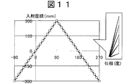
- FIG. 11 is a diagram showing the relationship between the incident coordinate of the light beam on the image surface of Example 1 and the phase.
- the incident angle is largely changed by the action of the free-form surface lens 2 and the free-form surface mirror 3 to realize the triangular wave-like incident coordinates on the image plane 20 in a range of ⁇ 300 mm. That is, while the scanning range is ⁇ 26.6 mm in the conventional method, it is ⁇ 300 mm in the first embodiment, realizing a widening of a wide angle of 10 times or more.
- the projection distance is defined by the length of a perpendicular drawn from the reference position that defines the arrangement position of the free-form curved mirror on the lens data to the image plane.
- the value of L / X may be increased within a range not exceeding 1.
- FIG. 12 shows the range of light rays where the principal ray coordinates exist as a result of light ray control by the free-form surface lens 2 and the free-form surface mirror 3. Since the long side direction of the optical scanning unit 1 is larger than the short side direction, the principal ray range on the fourth surface, which is the incident surface of the first free-form surface lens 2a, is a horizontally long region.
- the 8th surface which is the free-form curved mirror 3 is a vertically long region
- the long side direction (the horizontal direction in FIG. 12) is not extremely narrowed on the 8th surface, and the 8th surface is vertically long. This is a result of increasing the size as a degree of freedom. The reason for this will be described with reference to FIG.
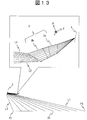
- FIG. 13 is a ray diagram in a cross section in the long side direction, and is a diagram that shows a ray diagram of the entire optical system and an enlarged view of the free-form surface lens 2 together.
- the light beam L1 passing through the positive side of the X axis in FIG. 13 by the rotation of the optical scanning unit 1 is reflected by the free-form surface mirror 3 and reaches the coordinate P1 of the image plane 20.
- the light beam L2 passing through the negative side of the X axis is reflected by the free-form surface mirror 3 and reaches the coordinate P2 of the image plane 20.
- the optical path of the light beam L2 passing through the free-form surface lens 2b and the light beam L1 reflected by the free-form surface mirror 3 does not interfere with the free-form surface lens 2b.
- the optical path length of the light beam L1 from the reflection by the free-form surface mirror 3 to the image plane is larger than the optical path length of the light beam L2. Therefore, in order to improve the linearity, it is necessary for the free-form surface lens 2 and the free-form surface mirror 3 to make the optical path length of the light beam L1 shorter than the optical path length of the light beam L2.
- the lens thickness on the side through which the light beam L1 passes is increased. ”Is necessary.
- FIG. 14 is a diagram of the sag amount in each optical element in the short side direction.
- FIG. 14 is a diagram showing the shape of the free-form surface lens and mirror in the short side direction.
- the first free-form surface lens 2a and the second free-form surface lens 2b in the short side direction are each a concave lens and have negative refractive power.
- the free-form surface mirror 3 has a positive refractive power because the central portion is concave, and has a negative refractive power because the peripheral portion is convex.
- the lens data of Example 1 has a plane-symmetric arrangement in the short side direction. By changing the plane-symmetric condition, that is, the arrangement relationship, the positive refractive power portion and the negative refraction are obtained. Since the force portion changes, it can be said that the free-form surface mirror 3 has a positive refractive power portion and a negative refractive power portion.
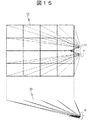
- Example 2 will be described with reference to FIGS. 15 is a ray diagram of Example 2, FIG. 16 is another ray diagram of Example 2, FIG. 17 is a detailed diagram of a free-form surface lens of Example 2, and FIG. 18 is a diagram showing lens data of Example 2. 19 is a diagram showing specific values of the free-form surface coefficients of the second embodiment, and FIG. 20 is a distortion performance diagram of the second embodiment.
- Example 3 will be described with reference to FIGS.
- FIG. 21 is a ray diagram of Example 3
- FIG. 22 is another ray diagram of Example 3
- FIG. 23 is a detailed diagram of a free-form surface lens of Example 3
- FIG. 24 is a diagram showing lens data of Example 3.
- 25 is a diagram showing specific values of the free-form surface coefficients of the third embodiment
- FIG. 26 is a distortion performance diagram of the third embodiment.
- the difference from the first embodiment is that the image plane size is 16: 9 according to the original wide screen, and the rotation angle of the optical scanning unit 1 (horizontal ⁇ 5.3 degrees, vertical ⁇ 2.9 degrees resonant rotation). ) In a two-dimensional range of 800 ⁇ 450 mm.
- the linearity that is the distortion performance of FIG. 26 is improved from that of FIG. 9 that shows the linearity that is the distortion performance of the first embodiment, and was originally developed to scan the image plane of 16: 9. In the case of 1, it is better to scan the 16: 9 image plane as a combination. Needless to say, the scanning mirror developed at 16: 9 can also be applied to a 4: 3 image plane.
- SYMBOLS 1 Optical scanning part, 2 ... Free-form surface lens, 3 ... Free-form surface mirror, 4 ... Light source, 10 ... Image display apparatus, 20 ... Image surface, 30 ... Structure, 1a ... Mirror, 1b ... 1st torsion spring, 1c ... holding member, 1d ... second torsion spring, 1e ... holding member.
Landscapes
- Physics & Mathematics (AREA)
- Optics & Photonics (AREA)
- General Physics & Mathematics (AREA)
- Engineering & Computer Science (AREA)
- Multimedia (AREA)
- Signal Processing (AREA)
- Mechanical Optical Scanning Systems (AREA)
Abstract
Description
図3は光線図であり、画像表示装置10から出射した光線が、像面20上の5×5の分割点に到達する様子を示している。図4は別の光線図であり、光源4から出射したレーザ光が光走査部1の回動で偏向された後、自由曲面レンズ2と自由曲面ミラー3を経て像面20に到達する様子を示している。更に、図5は自由曲面レンズ2の詳細図であり、第1の自由曲面レンズ2aと、第2の自由曲面レンズ2bで構成されている。
Claims (10)
- 光源から出射した光を、当該光の反射面の往復の回転運動により、像面の第1の方向及び第2の方向に走査する光走査部と、
走査された光の走査角度を拡大する光学系を備え、
前記光学系は、前記光走査部側に自由曲面レンズを有し、前記像面側に自由曲面ミラーを有する、画像表示装置。 - 前記第1の方向の長さは、前記第2の方向の長さよりも長く、
前記光走査部が走査範囲の中央で静止している場合の前記自由曲面ミラーにおける入射光線と反射光線で定義される第1の平面に対して、前記第1の方向が略平行となるように前記自由曲面ミラーが配置される、請求項1記載の画像表示装置。 - 前記光走査部は、2つの走査方向を有する1つの反射面を有する、請求項1又は2記載の画像表示装置。
- 前記光走査部は、1つの走査方向を有する1つの反射面を、それぞれ2つ有する、請求項1又は2記載の画像表示装置。
- 2つの走査方向における反射面の偏向角度のうちの大きい方向が、前記第1の方向に対応し、2つの走査方向における反射面の偏向角度のうちの小さい方向が、前記第2の方向に対応する、請求項1乃至4何れか一に記載の画像表示装置。
- 前記第1の平面における、前記自由曲面ミラー上での反射位置から前記像面上の走査位置までの距離が長い側の光線が前記自由曲面レンズを通過する光路長が、前記自由曲面ミラー上での反射位置から前記像面上の走査位置までの距離が短い側の光線が前記自由曲面レンズを通過する光路長よりも大きい、請求項1乃至5何れか一に記載の画像表示装置。
- 前記像面での前記第2の方向における前記自由曲面レンズが、負の屈折力を有する、請求項1乃至6何れか一に記載の画像表示装置。
- 前記像面での前記第2の方向における前記自由曲面ミラーの周辺部が、負の屈折力を有する、請求項1乃至6何れか一に記載の画像表示装置。
- 前記第1の方向の長さをX、レンズデータ上で自由曲面ミラーの配置位置を定義する基準位置から像面へ下ろした垂線の長さである投射距離をLとすると、L/Xは1以下である、請求項1乃至8何れか一に記載の画像表示装置。
- 前記第1の方向の長さをX、レンズデータ上で自由曲面ミラーの配置位置を定義する基準位置から像面へ下ろした垂線の長さである投射距離をLとすると、L/Xは0.2以下である、請求項1乃至8何れか一に記載の画像表示装置。
Priority Applications (3)
| Application Number | Priority Date | Filing Date | Title |
|---|---|---|---|
| PCT/JP2011/003284 WO2012168980A1 (ja) | 2011-06-10 | 2011-06-10 | 画像表示装置 |
| US14/124,779 US20140126032A1 (en) | 2011-06-10 | 2011-06-10 | Image display device |
| CN201180071068.3A CN103597398A (zh) | 2011-06-10 | 2011-06-10 | 图像显示装置 |
Applications Claiming Priority (1)
| Application Number | Priority Date | Filing Date | Title |
|---|---|---|---|
| PCT/JP2011/003284 WO2012168980A1 (ja) | 2011-06-10 | 2011-06-10 | 画像表示装置 |
Publications (1)
| Publication Number | Publication Date |
|---|---|
| WO2012168980A1 true WO2012168980A1 (ja) | 2012-12-13 |
Family
ID=47295590
Family Applications (1)
| Application Number | Title | Priority Date | Filing Date |
|---|---|---|---|
| PCT/JP2011/003284 Ceased WO2012168980A1 (ja) | 2011-06-10 | 2011-06-10 | 画像表示装置 |
Country Status (3)
| Country | Link |
|---|---|
| US (1) | US20140126032A1 (ja) |
| CN (1) | CN103597398A (ja) |
| WO (1) | WO2012168980A1 (ja) |
Cited By (1)
| Publication number | Priority date | Publication date | Assignee | Title |
|---|---|---|---|---|
| JP2014164047A (ja) * | 2013-02-22 | 2014-09-08 | Stanley Electric Co Ltd | 光スキャナ |
Families Citing this family (8)
| Publication number | Priority date | Publication date | Assignee | Title |
|---|---|---|---|---|
| WO2012176235A1 (ja) * | 2011-06-22 | 2012-12-27 | 日立コンシューマエレクトロニクス株式会社 | 画像表示装置 |
| KR20150116302A (ko) * | 2014-04-07 | 2015-10-15 | 엘지전자 주식회사 | 영상표시장치, 및 그 동작방법 |
| CN104464523B (zh) * | 2015-01-06 | 2017-03-15 | 京东方科技集团股份有限公司 | 曲面显示装置 |
| JP2017125942A (ja) | 2016-01-14 | 2017-07-20 | ソニー株式会社 | レンズモジュール、およびプロジェクタ |
| US10890833B2 (en) * | 2016-01-19 | 2021-01-12 | Maxell, Ltd. | Projection-type image apparatus |
| WO2018015991A1 (ja) * | 2016-07-19 | 2018-01-25 | マクセル株式会社 | 投写型映像表示装置 |
| CN110873961B (zh) * | 2018-08-31 | 2022-03-04 | 成都理想境界科技有限公司 | 一种光纤扫描显示装置及设备、扫描方法 |
| JP7722107B2 (ja) * | 2021-09-30 | 2025-08-13 | セイコーエプソン株式会社 | プロジェクション装置及びプロジェクション装置の制御方法 |
Citations (4)
| Publication number | Priority date | Publication date | Assignee | Title |
|---|---|---|---|---|
| WO2005083493A1 (ja) * | 2004-02-27 | 2005-09-09 | Matsushita Electric Industrial Co., Ltd. | 照明光源及びそれを用いた2次元画像表示装置 |
| JP2006178346A (ja) * | 2004-12-24 | 2006-07-06 | Canon Inc | 光走査装置及びそれを用いた画像表示装置 |
| WO2009041342A1 (ja) * | 2007-09-26 | 2009-04-02 | Konica Minolta Opto, Inc. | 走査型投射装置 |
| JP2010049232A (ja) * | 2008-07-23 | 2010-03-04 | Ricoh Co Ltd | 光走査装置、これを用いた画像投影装置、ヘッドアップディスプレイ装置および携帯電話機 |
Family Cites Families (3)
| Publication number | Priority date | Publication date | Assignee | Title |
|---|---|---|---|---|
| JP2006292900A (ja) * | 2005-04-08 | 2006-10-26 | Hitachi Ltd | 投写光学ユニット及びそれを用いた投写型映像表示装置 |
| JP4853033B2 (ja) * | 2005-04-21 | 2012-01-11 | セイコーエプソン株式会社 | 光走査装置及び画像表示装置 |
| JP4464948B2 (ja) * | 2006-10-13 | 2010-05-19 | 株式会社日立製作所 | 投写型映像表示システム |
-
2011
- 2011-06-10 US US14/124,779 patent/US20140126032A1/en not_active Abandoned
- 2011-06-10 CN CN201180071068.3A patent/CN103597398A/zh active Pending
- 2011-06-10 WO PCT/JP2011/003284 patent/WO2012168980A1/ja not_active Ceased
Patent Citations (4)
| Publication number | Priority date | Publication date | Assignee | Title |
|---|---|---|---|---|
| WO2005083493A1 (ja) * | 2004-02-27 | 2005-09-09 | Matsushita Electric Industrial Co., Ltd. | 照明光源及びそれを用いた2次元画像表示装置 |
| JP2006178346A (ja) * | 2004-12-24 | 2006-07-06 | Canon Inc | 光走査装置及びそれを用いた画像表示装置 |
| WO2009041342A1 (ja) * | 2007-09-26 | 2009-04-02 | Konica Minolta Opto, Inc. | 走査型投射装置 |
| JP2010049232A (ja) * | 2008-07-23 | 2010-03-04 | Ricoh Co Ltd | 光走査装置、これを用いた画像投影装置、ヘッドアップディスプレイ装置および携帯電話機 |
Cited By (1)
| Publication number | Priority date | Publication date | Assignee | Title |
|---|---|---|---|---|
| JP2014164047A (ja) * | 2013-02-22 | 2014-09-08 | Stanley Electric Co Ltd | 光スキャナ |
Also Published As
| Publication number | Publication date |
|---|---|
| US20140126032A1 (en) | 2014-05-08 |
| CN103597398A (zh) | 2014-02-19 |
Similar Documents
| Publication | Publication Date | Title |
|---|---|---|
| US7957047B2 (en) | Laser projection device | |
| KR101193524B1 (ko) | 광 주사 유닛, 이를 포함하는 화상 투영 장치, 차량 헤드업 디스플레이 장치 및 휴대 전화기 | |
| JP4266660B2 (ja) | 投射型表示光学系および投射型画像表示装置 | |
| US20140126032A1 (en) | Image display device | |
| US9405121B2 (en) | Image display apparatus and head-mounted display | |
| CN109477961B (zh) | 投射型影像显示装置 | |
| CN102132191B (zh) | 激光投射装置 | |
| US7385745B2 (en) | Two-dimensional scanning apparatus and scanning type image displaying apparatus using the same | |
| CN103454765A (zh) | 图像显示装置以及头戴式显示器 | |
| JP7459580B2 (ja) | 可動装置、画像投影装置、ヘッドアップディスプレイ、レーザヘッドランプ、ヘッドマウントディスプレイ、物体認識装置、及び移動体 | |
| JP7202539B2 (ja) | 画像表示装置、画像投写装置及び移動体 | |
| US10598950B2 (en) | Image projection apparatus and movable body | |
| WO2019181749A1 (en) | Image projection device and mobile body | |
| US6859329B2 (en) | Scanning type display optical system and scanning type image display apparatus | |
| JP2017009635A (ja) | 圧電アクチュエータ装置、光偏向器、画像投影装置及び画像形成装置 | |
| JP4962002B2 (ja) | レーザ投射装置 | |
| US10989918B2 (en) | Optical scanner, image display device, head-mounted display, and heads-up display | |
| JPWO2012168980A1 (ja) | 画像表示装置 | |
| CN111868607B (zh) | 图像显示设备、图像投影设备和移动体 | |
| KR102331643B1 (ko) | 스캐닝 마이크로미러 | |
| EP3012678A1 (en) | Light-deflection element, light-deflector, two-dimensional imaging display, optical scanning device, and image forming device | |
| JP2007163817A (ja) | 光偏向器、及びそれを用いた光学機器 | |
| JP2024015968A (ja) | 可動装置、光走査システム、ヘッドアップディスプレイ、レーザヘッドランプ、ヘッドマウントディスプレイ、物体認識装置および移動体。 | |
| JP2023138313A (ja) | 可動装置、光走査システム、ヘッドアップディスプレイ、レーザヘッドランプ、ヘッドマウントディスプレイ、物体認識装置および移動体。 | |
| JP2013125109A (ja) | 3次元画像表示装置および3次元画像表示方法 |
Legal Events
| Date | Code | Title | Description |
|---|---|---|---|
| 121 | Ep: the epo has been informed by wipo that ep was designated in this application |
Ref document number: 11867233 Country of ref document: EP Kind code of ref document: A1 |
|
| WWE | Wipo information: entry into national phase |
Ref document number: 14124779 Country of ref document: US |
|
| NENP | Non-entry into the national phase |
Ref country code: DE |
|
| ENP | Entry into the national phase |
Ref document number: 2013519238 Country of ref document: JP Kind code of ref document: A |
|
| 122 | Ep: pct application non-entry in european phase |
Ref document number: 11867233 Country of ref document: EP Kind code of ref document: A1 |