WO2012168959A1 - 半導体チップ、これを備えた半導体装置および半導体チップの製造方法 - Google Patents
半導体チップ、これを備えた半導体装置および半導体チップの製造方法 Download PDFInfo
- Publication number
- WO2012168959A1 WO2012168959A1 PCT/JP2011/003169 JP2011003169W WO2012168959A1 WO 2012168959 A1 WO2012168959 A1 WO 2012168959A1 JP 2011003169 W JP2011003169 W JP 2011003169W WO 2012168959 A1 WO2012168959 A1 WO 2012168959A1
- Authority
- WO
- WIPO (PCT)
- Prior art keywords
- semiconductor chip
- chip
- semiconductor
- wafer
- dicing
- Prior art date
- Legal status (The legal status is an assumption and is not a legal conclusion. Google has not performed a legal analysis and makes no representation as to the accuracy of the status listed.)
- Ceased
Links
Images


Classifications
-
- H—ELECTRICITY
- H10—SEMICONDUCTOR DEVICES; ELECTRIC SOLID-STATE DEVICES NOT OTHERWISE PROVIDED FOR
- H10W—GENERIC PACKAGES, INTERCONNECTIONS, CONNECTORS OR OTHER CONSTRUCTIONAL DETAILS OF DEVICES COVERED BY CLASS H10
- H10W72/00—Interconnections or connectors in packages
- H10W72/30—Die-attach connectors
-
- H—ELECTRICITY
- H10—SEMICONDUCTOR DEVICES; ELECTRIC SOLID-STATE DEVICES NOT OTHERWISE PROVIDED FOR
- H10D—INORGANIC ELECTRIC SEMICONDUCTOR DEVICES
- H10D62/00—Semiconductor bodies, or regions thereof, of devices having potential barriers
- H10D62/10—Shapes, relative sizes or dispositions of the regions of the semiconductor bodies; Shapes of the semiconductor bodies
- H10D62/117—Shapes of semiconductor bodies
-
- H—ELECTRICITY
- H10—SEMICONDUCTOR DEVICES; ELECTRIC SOLID-STATE DEVICES NOT OTHERWISE PROVIDED FOR
- H10P—GENERIC PROCESSES OR APPARATUS FOR THE MANUFACTURE OR TREATMENT OF DEVICES COVERED BY CLASS H10
- H10P72/00—Handling or holding of wafers, substrates or devices during manufacture or treatment thereof
- H10P72/70—Handling or holding of wafers, substrates or devices during manufacture or treatment thereof for supporting or gripping
- H10P72/74—Handling or holding of wafers, substrates or devices during manufacture or treatment thereof for supporting or gripping using temporarily an auxiliary support
- H10P72/7402—Wafer tapes, e.g. grinding or dicing support tapes
-
- H—ELECTRICITY
- H10—SEMICONDUCTOR DEVICES; ELECTRIC SOLID-STATE DEVICES NOT OTHERWISE PROVIDED FOR
- H10P—GENERIC PROCESSES OR APPARATUS FOR THE MANUFACTURE OR TREATMENT OF DEVICES COVERED BY CLASS H10
- H10P72/00—Handling or holding of wafers, substrates or devices during manufacture or treatment thereof
- H10P72/70—Handling or holding of wafers, substrates or devices during manufacture or treatment thereof for supporting or gripping
- H10P72/74—Handling or holding of wafers, substrates or devices during manufacture or treatment thereof for supporting or gripping using temporarily an auxiliary support
- H10P72/7416—Handling or holding of wafers, substrates or devices during manufacture or treatment thereof for supporting or gripping using temporarily an auxiliary support used during dicing or grinding
-
- H—ELECTRICITY
- H10—SEMICONDUCTOR DEVICES; ELECTRIC SOLID-STATE DEVICES NOT OTHERWISE PROVIDED FOR
- H10P—GENERIC PROCESSES OR APPARATUS FOR THE MANUFACTURE OR TREATMENT OF DEVICES COVERED BY CLASS H10
- H10P72/00—Handling or holding of wafers, substrates or devices during manufacture or treatment thereof
- H10P72/70—Handling or holding of wafers, substrates or devices during manufacture or treatment thereof for supporting or gripping
- H10P72/74—Handling or holding of wafers, substrates or devices during manufacture or treatment thereof for supporting or gripping using temporarily an auxiliary support
- H10P72/7422—Handling or holding of wafers, substrates or devices during manufacture or treatment thereof for supporting or gripping using temporarily an auxiliary support used to protect an active side of a device or wafer
-
- H—ELECTRICITY
- H10—SEMICONDUCTOR DEVICES; ELECTRIC SOLID-STATE DEVICES NOT OTHERWISE PROVIDED FOR
- H10P—GENERIC PROCESSES OR APPARATUS FOR THE MANUFACTURE OR TREATMENT OF DEVICES COVERED BY CLASS H10
- H10P72/00—Handling or holding of wafers, substrates or devices during manufacture or treatment thereof
- H10P72/70—Handling or holding of wafers, substrates or devices during manufacture or treatment thereof for supporting or gripping
- H10P72/74—Handling or holding of wafers, substrates or devices during manufacture or treatment thereof for supporting or gripping using temporarily an auxiliary support
- H10P72/744—Details of chemical or physical process used for separating the auxiliary support from a device or a wafer
-
- H—ELECTRICITY
- H10—SEMICONDUCTOR DEVICES; ELECTRIC SOLID-STATE DEVICES NOT OTHERWISE PROVIDED FOR
- H10P—GENERIC PROCESSES OR APPARATUS FOR THE MANUFACTURE OR TREATMENT OF DEVICES COVERED BY CLASS H10
- H10P72/00—Handling or holding of wafers, substrates or devices during manufacture or treatment thereof
- H10P72/70—Handling or holding of wafers, substrates or devices during manufacture or treatment thereof for supporting or gripping
- H10P72/74—Handling or holding of wafers, substrates or devices during manufacture or treatment thereof for supporting or gripping using temporarily an auxiliary support
- H10P72/744—Details of chemical or physical process used for separating the auxiliary support from a device or a wafer
- H10P72/7442—Separation by peeling
-
- H—ELECTRICITY
- H10—SEMICONDUCTOR DEVICES; ELECTRIC SOLID-STATE DEVICES NOT OTHERWISE PROVIDED FOR
- H10W—GENERIC PACKAGES, INTERCONNECTIONS, CONNECTORS OR OTHER CONSTRUCTIONAL DETAILS OF DEVICES COVERED BY CLASS H10
- H10W72/00—Interconnections or connectors in packages
- H10W72/50—Bond wires
- H10W72/551—Materials of bond wires
- H10W72/552—Materials of bond wires comprising metals or metalloids, e.g. silver
- H10W72/5522—Materials of bond wires comprising metals or metalloids, e.g. silver comprising gold [Au]
-
- H—ELECTRICITY
- H10—SEMICONDUCTOR DEVICES; ELECTRIC SOLID-STATE DEVICES NOT OTHERWISE PROVIDED FOR
- H10W—GENERIC PACKAGES, INTERCONNECTIONS, CONNECTORS OR OTHER CONSTRUCTIONAL DETAILS OF DEVICES COVERED BY CLASS H10
- H10W72/00—Interconnections or connectors in packages
- H10W72/851—Dispositions of multiple connectors or interconnections
- H10W72/874—On different surfaces
- H10W72/884—Die-attach connectors and bond wires
-
- H—ELECTRICITY
- H10—SEMICONDUCTOR DEVICES; ELECTRIC SOLID-STATE DEVICES NOT OTHERWISE PROVIDED FOR
- H10W—GENERIC PACKAGES, INTERCONNECTIONS, CONNECTORS OR OTHER CONSTRUCTIONAL DETAILS OF DEVICES COVERED BY CLASS H10
- H10W74/00—Encapsulations, e.g. protective coatings
-
- H—ELECTRICITY
- H10—SEMICONDUCTOR DEVICES; ELECTRIC SOLID-STATE DEVICES NOT OTHERWISE PROVIDED FOR
- H10W—GENERIC PACKAGES, INTERCONNECTIONS, CONNECTORS OR OTHER CONSTRUCTIONAL DETAILS OF DEVICES COVERED BY CLASS H10
- H10W74/00—Encapsulations, e.g. protective coatings
- H10W74/10—Encapsulations, e.g. protective coatings characterised by their shape or disposition
- H10W74/111—Encapsulations, e.g. protective coatings characterised by their shape or disposition the semiconductor body being completely enclosed
- H10W74/114—Encapsulations, e.g. protective coatings characterised by their shape or disposition the semiconductor body being completely enclosed by a substrate and the encapsulations
-
- H—ELECTRICITY
- H10—SEMICONDUCTOR DEVICES; ELECTRIC SOLID-STATE DEVICES NOT OTHERWISE PROVIDED FOR
- H10W—GENERIC PACKAGES, INTERCONNECTIONS, CONNECTORS OR OTHER CONSTRUCTIONAL DETAILS OF DEVICES COVERED BY CLASS H10
- H10W90/00—Package configurations
- H10W90/701—Package configurations characterised by the relative positions of pads or connectors relative to package parts
- H10W90/751—Package configurations characterised by the relative positions of pads or connectors relative to package parts of bond wires
- H10W90/754—Package configurations characterised by the relative positions of pads or connectors relative to package parts of bond wires between a chip and a stacked insulating package substrate, interposer or RDL
Definitions
- the present invention relates to a semiconductor chip bonded and fixed on a chip support substrate via a die bond material, a semiconductor device including the semiconductor chip, and a method for manufacturing the semiconductor chip.
- a chip mounting portion having a chip supporting surface, a plurality of leads arranged around the chip mounting portion, and a semiconductor chip bonded and fixed to the chip supporting surface of the chip mounting portion via a paste material And a wire for connecting the semiconductor chip and the plurality of leads, and a sealing body for resin-sealing the plurality of leads, the semiconductor chip and the wire on the chip mounting portion (Patent Document) 1).
- the outer size of the chip support surface is formed smaller than the back surface size of the semiconductor chip, and a step portion lower than this is formed on the peripheral portion of the chip support surface. This prevents the die bond material from flowing out to the back surface of the sealing body and improves the quality and reliability of the semiconductor chip.
- the convex portion needs to be processed on a single chip mounting portion, and must be formed while avoiding a lead or the like in position, so that chip mounting is possible in terms of processing efficiency and positional constraints. There was a problem that the processing of the part became complicated.
- the semiconductor chip of the present invention is a semiconductor chip that is bonded and fixed onto a chip support substrate via a die bond material, and the back side of the semiconductor chip that is bonded and fixed to the chip support substrate is formed from an adhesive portion and a non-adhesive portion. It is formed in the uneven
- the back surface side of the semiconductor chip is formed in a concavo-convex shape composed of an adhesive portion and a non-adhesion portion
- the chip support substrate and the chip support substrate are compared with the case where the entire back surface side is flat (adhesion portion).
- the contact area (adhesion area) can be reduced.
- the stress to the semiconductor chip caused by the secondary mounting can be reduced. That is, the physical and electrical effects on the semiconductor chip during secondary mounting can be reduced, and the quality and reliability of the semiconductor chip itself can be improved.
- the semiconductor chip side has a concavo-convex shape, positional flexibility of the formed bonded portion and non-bonded portion is increased, and processing is not complicated.
- the non-bonded portion is formed on at least one of the two peripheral edges on the back side of the semiconductor chip.
- the non-adhesive portion can be formed in a balanced manner at the symmetrical position on the back surface side of the semiconductor chip, and the non-contact portion can be easily formed on the semiconductor chip.
- the non-bonded portion is preferably a groove formed by grinding in a wafer level state before chip formation.
- non-contact portions can be collectively formed on a plurality of semiconductor chips, and non-adhesion portions can be easily formed.
- the semiconductor device of the present invention includes the above-described semiconductor chip, a chip support substrate that supports the semiconductor chip, a die bond material that adheres and fixes the semiconductor chip to the chip support substrate, and a seal that seals the semiconductor chip on the chip support substrate. And a material.
- the semiconductor device capable of reducing stress on the semiconductor chip in the secondary mounting.
- the physical and electrical effects on the semiconductor chip during secondary mounting can be reduced, and the quality and reliability of the semiconductor device itself can be improved.
- it is preferable to use a silver paste as the die bond material and it is preferable to apply the silver paste so as to wrap around in a fillet shape from the bonded portion toward the non-bonded portion in order to increase the adhesive strength.
- a method for manufacturing a semiconductor chip according to the present invention is a method for manufacturing a semiconductor chip, in which a plurality of semiconductor chips are obtained by dividing a wafer having a plurality of semiconductor elements formed in a matrix on the surface. Using a blade, the wafer bonded to the dicing tape is divided into chips, and prior to the dicing process, a dicing blade for groove processing is used to reverse the front and back and attach the wafer to the dicing tape. And a groove forming step for forming a groove to become.
- the wafer is formed into chips after forming the grooves to be non-adhered portions on the wafer, the semiconductor chip in which the adhering portions and the non-adhering portions are easily formed collectively, That is, it is possible to manufacture a semiconductor chip that can reduce stress in the secondary mounting.
- the degree of freedom in design such as the groove formation position and groove width can be increased.
- the dicing tape at the time of groove formation is peeled off (UV irradiation or the like) after the wafer is turned upside down and attached to the dicing tape for separation (breaking prevention at the groove portion).
- the dicing process is divided along the vertical dividing line and the horizontal dividing line, and the groove forming process is preferably formed with a groove along at least one of the vertical dividing line and the horizontal dividing line.
- the non-adhered portions (grooves) of adjacent semiconductor chips can be formed at the same time, and a semiconductor chip having a symmetrical non-adhered portion can be easily manufactured. Further, grooves are formed along vertical and horizontal dividing lines (scribe lines), and division (dicing) is performed along vertical and horizontal dividing lines, so that the depth of cut at the dividing can be made relatively shallow. It is possible to prevent a large chipping from occurring.
- a semiconductor chip is packaged in a surface-mounted BGA (Ball Grid Array) package, and the semiconductor chip is composed of, for example, an analog IC.
- BGA Bit Grid Array
- the semiconductor device 1 includes a semiconductor chip 2, a chip support substrate 3 that supports the semiconductor chip 2, a die bond material 4 that adheres and fixes the semiconductor chip 2 to the chip support substrate 3, and a chip support substrate 3. And a sealing material 5 for sealing the semiconductor chip 2.
- the chip support substrate 3 is a so-called glass epoxy substrate, and electrodes 12 are embedded in a plurality of contact holes 11 penetrating in the front and back directions.
- a bonding pad 13 is formed at the upper end of each electrode 12, and a solder bump 14 is formed at the lower end, thereby constituting a surface mount type package.
- the semiconductor chip 2 and each bonding pad 13 are connected by a loop-shaped wire 15 (gold wire), and the semiconductor chip 2 and the plurality of wires 15 are molded and sealed with a resin that is a sealing material 5.
- the chip support substrate 3 may be a lead frame or the like.
- the sealing material 5 may be a lid-like case.
- the semiconductor chip 2 is formed by scribing (chip-forming) a wafer 16 on a surface of which a plurality of semiconductor elements are formed in a matrix by repeating film formation, lithography, impurity diffusion, and the like.
- the thing is comprised by analog IC, for example.
- the back surface side of the semiconductor chip 2 is formed in a concavo-convex shape composed of an adhesive portion 17 and a non-adhesive portion 18, and the semiconductor chip 2 is connected to the die bond material 4 (adhesive) such as silver paste via the adhesive portion 17. ) Is bonded and fixed (primary mounting) on the chip support substrate 3.
- a square bonding portion 17 is formed at the center thereof, and there is a step portion around the bonding portion 17, that is, at the four peripheral edges of the back surface, and is not bonded.
- a portion 18 is formed.
- the chip support substrate 3 is coated with an amount of die bond material 4 that protrudes from the bonding portion 17.
- the die bond material 4 that protrudes extends from the bonding portion 17 toward the non-bonding portion 18. It is designed to wrap around the shape. Thereby, even if the bonding area of the bonding portion 17 is small, the semiconductor chip 2 is firmly bonded and fixed to the chip support substrate 3.
- the semiconductor device 1 configured as described above is secondarily mounted (mounted) on a printed circuit board 19 (printed circuit board) or the like.
- a printed circuit board 19 printed circuit board
- the semiconductor chip 2 of the present embodiment having the non-bonded portion 18 on the back surface side, since the bonding area with the chip support substrate 3 can be reduced, the stress on the semiconductor chip 2 caused by secondary mounting is reduced. be able to. That is, the physical influence and electrical influence on the semiconductor chip 2 at the time of secondary mounting can be reduced as much as possible.
- the manufacturing method relates to a dicing process (a dicing process in a broad sense) in a post-process of semiconductor manufacturing, and a wafer 16 having a plurality of semiconductor elements 21 formed in a matrix on the surface is divided into a matrix by a dicing apparatus.
- a plurality of semiconductor chips 2 are obtained by (chiping).
- the dicing apparatus includes, for example, a dicing tape 22 (UV tape), an X / Y / ⁇ axis table on which the wafer 16 is set, and dicing blades 23 and 24 detachably attached to the spindle.
- a Z-axis table for finely moving the dicing blades 23 and 24 in the Z-axis direction via the spindle, and a recognition camera for recognizing the image of the wafer 16.
- the wafer 16 introduced into the dicing apparatus is polished (back-ground) in advance so as to have a predetermined thickness.
- the dicing blade 23 for cutting is used to divide the wafer 16 adhered to the dicing tape 22 into chips, and the dicing blade 24 for grooving is formed prior to the dicing process.
- image recognition is performed in advance by a recognition camera on the wafer 16 set on the X, Y, and ⁇ axis tables via the dicing tape 22, and the alignment of the wafer 16 is performed based on the recognition result. Performed (micro movement or data correction by X, Y, ⁇ axis table).
- the dicing step and the groove forming step are performed based on scribe data (scribe line and cutting depth data) input in advance.
- the dicing blade 24 for groove processing is mounted on the spindle, and the wafer 16 is attached to the X / Y / ⁇ axis table with the surface 25 on the element forming side as the lower surface using the dicing tape 22. (FIG. 3A). Then, after the alignment described above, a groove that becomes the non-bonded portion 18 is formed by following the vertical dividing line and the horizontal dividing line based on the scribe data by using the dicing blade 24 for groove processing (FIG. 3B).
- channel used as said non-bonding part 18 is formed.
- the width of the groove serving as the non-bonded portion 18 is about 300 ⁇ m and the depth thereof is about 50 ⁇ m (the thickness of the wafer 16 is 300 ⁇ m).
- the wafer 16 on which the groove to be the non-adhesive portion 18 is formed is reversed and set again on the X, Y, ⁇ axis table.
- the wafer 16 is attached to the dicing tape 22.
- the dicing tape 22 is preferably reset. That is, it is preferable to peel the dicing tape 22 by resetting the wafer 16 and then irradiating it with ultraviolet rays from above. As a result, it is possible to prevent the wafer 16 from breaking at the groove portion during handling associated with the resetting.
- the wafer 16 may be reset after being peeled from the dicing tape 22. It is also preferable to perform an appearance inspection using a recognition camera immediately after the groove formation is completed.
- a cutting dicing blade 23 is attached to the spindle in place of the groove processing dicing blade 24, and a new dicing tape 22 is used to form the element forming side on the X, Y, ⁇ axis table.
- the wafer 16 is attached with the surface 25 as the upper surface (FIG. 3C).
- the cutting dicing blade 23 performs cutting according to the vertical cutting line and the horizontal cutting line based on the scribe data, and the wafer 16 is formed into chips (FIG. 3D).
- the black matrix portion of the wafer 16 is diced along each longitudinal dividing line to divide the wafer 16 into strips, and then the wafer 16 is rotated by 90 ° and then diced along each horizontal dividing line. Then, the wafer 16 is divided into a matrix.
- the dividing width (cutting allowance) by the dividing dicing blade 23 is generally about 30 ⁇ m.
- the appearance inspection is performed using the recognition camera, and the dicing tape 22 is irradiated with ultraviolet rays from below to reduce the adhesive force of the dicing tape 22 so that each semiconductor chip 2 can be peeled off.
- the defective semiconductor chip 2 is picked up and removed by the continuity inspection and the appearance inspection performed before the dicing process in a broad sense, and the process proceeds to a die bonding process (primary mounting) as the next process.
- a groove forming the non-bonded portion 18 may be formed by performing the groove forming process following only the vertical dividing line or the horizontal dividing line (see FIG. 4A). Moreover, you may make it form the groove
- the back surface side of the semiconductor chip is formed into a concavo-convex shape consisting of an adhesive part and a non-adhesive part by simple processing, so the contact area with the chip support substrate is reduced, and secondary mounting It is possible to reduce the stress on the semiconductor chip caused by the above.
Landscapes
- Dicing (AREA)
Abstract
本発明は、簡単な加工により、二次実装により生ずる半導体チップへの応力の影響を軽減することができる半導体チップ、これを備えた半導体装置および半導体チップの製造方法を提供することを課題としている。 本発明の半導体チップは、ダイボンド材を介して、チップ支持基板上に接着固定される半導体チップであって、チップ支持基板に接着固定される半導体チップの裏面側が、接着部と非接着部とから成る凹凸形状に形成されていることを特徴とする。
Description
本発明は、ダイボンド材を介して、チップ支持基板上に接着固定される半導体チップ、これを備えた半導体装置および半導体チップの製造方法に関するものである。
従来、この種の半導体装置として、チップ支持面を有するチップ搭載部と、チップ搭載部の周囲に配置した複数のリードと、ペースト材を介してチップ搭載部のチップ支持面に接着固定した半導体チップと、半導体チップと複数のリードとを接続するワイヤと、複数のリード、半導体チップおよびワイヤをチップ搭載部上に樹脂封止する封止体と、を備えたものが知られている(特許文献1参照)。
また、この半導体装置では、チップ支持面の外形サイズが、半導体チップの裏面サイズより小さく形成され、且つチップ支持面の周縁部に、これより低い段差部が形成されている。
これにより、封止体の裏面へのダイボンド材の流出を防止し、半導体チップの品質や信頼性を向上するようにしている。
また、この半導体装置では、チップ支持面の外形サイズが、半導体チップの裏面サイズより小さく形成され、且つチップ支持面の周縁部に、これより低い段差部が形成されている。
これにより、封止体の裏面へのダイボンド材の流出を防止し、半導体チップの品質や信頼性を向上するようにしている。
ところで、この種の半導体装置において、特にアナログIC等では、回路基板にマウント(二次実装)するときに、半田実装時の熱的影響や熱収縮に基づく残留応力により、チップ搭載部(チップ支持基板)を介して半導体チップに物理的影響および電気的影響を及ぼすことが知られている。すなわち、マウント時の残留応力等により、半導体チップが剥がれたり、半導体チップ(アナログIC)の出力信号に不具合が生ずる。
上記従来の半導体装置では、チップ支持面の外形サイズが、半導体チップの裏面サイズより小さく形成されているため、チップ搭載部(チップ支持基板)と半導体チップとの接着面積が小さくなり、半導体チップに対するチップ搭載部からの応力を軽減することができる。
しかし、チップ搭載部(チップ支持基板)に段差部、言い換えればチップ支持面となる凸部を形成する必要があり、チップ搭載部の加工が煩雑になる問題があった。すなわち、この凸部は、単体のチップ搭載部に対し加工を行う必要があると共に、位置的にリード等を回避して形成する必要があり、加工効率や位置的制約等の点で、チップ搭載部の加工が煩雑になる問題があった。
上記従来の半導体装置では、チップ支持面の外形サイズが、半導体チップの裏面サイズより小さく形成されているため、チップ搭載部(チップ支持基板)と半導体チップとの接着面積が小さくなり、半導体チップに対するチップ搭載部からの応力を軽減することができる。
しかし、チップ搭載部(チップ支持基板)に段差部、言い換えればチップ支持面となる凸部を形成する必要があり、チップ搭載部の加工が煩雑になる問題があった。すなわち、この凸部は、単体のチップ搭載部に対し加工を行う必要があると共に、位置的にリード等を回避して形成する必要があり、加工効率や位置的制約等の点で、チップ搭載部の加工が煩雑になる問題があった。
本発明は、簡単な加工により、二次実装により生ずる半導体チップへの応力の影響を軽減することができる半導体チップ、これを備えた半導体装置および半導体チップの製造方法を提供することを課題としている。
本発明の半導体チップは、ダイボンド材を介して、チップ支持基板上に接着固定される半導体チップであって、チップ支持基板に接着固定される半導体チップの裏面側が、接着部と非接着部とから成る凹凸形状に形成されていることを特徴とする。
この構成によれば、半導体チップの裏面側が、接着部と非接着部とから成る凹凸形状に形成されているため、裏面側全体が平坦(接着部)な場合に比して、チップ支持基板との接触面積(接着面積)を小さくすることができる。これにより、二次実装(回路基板へのマウント)により生じる半導体チップへの応力を軽減させることができる。すなわち、二次実装時の半導体チップへの物理的影響および電気的影響を軽減することができ、半導体チップ自体の品質や信頼性を向上させることができる。また、半導体チップ側を凹凸形状としているため、形成される接着部および非接着部の位置的自由度が増すと共に、加工が煩雑になることもない。
この場合、非接着部は、半導体チップの裏面側における4辺の周縁部うち少なくとも一方の平行な2辺の周縁部に形成されていることが好ましい。
この構成によれば、半導体チップの裏面側対称位置に非接着部をバランス良く形成することができると共に、半導体チップに対して非接触部を簡単に形成することができる。
この場合、非接着部は、チップ化前のウェーハレベルの状態で、研削により形成した溝であることが好ましい。
この構成によれば、ウェーハレベルで溝を研削することにより、複数の半導体チップに対し非接触部を一括して形成することができ、非接着部を簡単に形成することができる。なお、溝の研削は、半導体チップの分断前に行うことが好ましい。
本発明の半導体装置は、上記の半導体チップと、半導体チップを支持するチップ支持基板と、半導体チップをチップ支持基板に接着固定するダイボンド材と、チップ支持基板上に半導体チップを封止する封止材と、を備えたことを特徴とする。
この構成によれば、二次実装において、半導体チップに対する応力を軽減し得る半導体装置を提供することができる。これにより、二次実装時の半導体チップへの物理的影響および電気的影響を軽減することができ、半導体装置自体の品質や信頼性を向上させることができる。なお、ダイボンド材として、銀ペーストを用いることが好ましく、且つ銀ペーストは、接着強度をアップさせるべく、接着部から非接着部に向ってフィレット形状に回り込むように塗着させることが好ましい。
本発明の半導体チップの製造方法は、表面に複数の半導体素子をマトリクス状に作り込んだウェーハを分断して、上記の半導体チップの複数個を得る半導体チップの製造方法であって、分断用ダイシングブレードを用い、ダイシングテープに貼着したウェーハを分断しチップ化するダイシング工程と、ダイシング工程に先立ち、溝加工用ダイシングブレードを用い、表裏反転してダイシングテープに貼着したウェーハに、非接着部となる溝を形成する溝形成工程と、を備えたことを特徴とする。
この構成によれば、ウェーハに対して、非接着部となる溝を形成した後、ウェーハをチップ化するようにしているため、一括して簡単に接着部および非接着部を形成した半導体チップ、すなわち二次実装において応力を軽減し得る半導体チップを製造することができる。また、溝の形成位置や溝の幅等の設計の自由度を高めることができる。なお、溝の形成直後およびウェーハの分断直後に、それぞれ外観検査を行うことが好ましい。また、溝形成時のダイシングテープは、分断のためにウェーハを表裏反転してダイシングテープに貼着してから、剥がす(UV照射等)ことが好ましい(溝部分でのブレイク防止)。
この場合、ダイシング工程では、縦分断ラインおよび横分断ラインに倣って分断が行われ、溝形成工程では、縦分断ラインおよび横分断ラインの少なくとも一方に倣って溝が形成されることが好ましい。
この構成によれば、隣接する半導体チップの非接着部(溝)を同時に形成することができ、対称的な非接着部が形成された半導体チップを簡単に製造することができる。また、縦横の分断ライン(スクライブライン)に倣って溝の形成が行われ、且つ縦横の分断ラインに倣って分断(ダイシング)が行われるため、分断における切込み深さを相対的に浅くすることができ、大きなチッピング(欠け)が生ずるのを未然に防止することができる。
以下、添付した図面を参照して、本発明の一実施形態に係る半導体チップ、これを備えた半導体装置および半導体製造装置について説明する。この半導体装置は、半導体チップを表面実装型のBGA(Ball Grid Array)パッケージでパッケージングしたものであり、半導体チップは、例えばアナログICで構成されている。
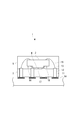
図1に示すように、半導体装置1は、半導体チップ2と、半導体チップ2を支持するチップ支持基板3と、半導体チップ2をチップ支持基板3に接着固定するダイボンド材4と、チップ支持基板3上に半導体チップ2を封止する封止材5と、を備えている。
チップ支持基板3は、いわゆるガラスエポキシ基板であり、表裏方向に貫通する複数のコンタクトホール11には、それぞれ電極12が埋め込まれている。各電極12の上端には、ボンディングパッド13が形成され、下端には半田バンプ14が形成されていて、表面実装型のパッケージを構成している。半導体チップ2と各ボンディングパッド13は、ループ形状のワイヤ15(金線)で接続されており、この半導体チップ2と複数のワイヤ15は、封止材5である樹脂でモールド封止されている。なお、チップ支持基板3がリードフレーム等であってもよい。また、封止材5は蓋状のケースであってもよい。
半導体チップ2は、表面に、成膜、リソグラフィ、不純物拡散等を繰り返して複数の半導体素子をマトリクス状に形成したウェーハ16を、スクライビング(チップ化)して、形成したものであり、実施形態のものは、例えばアナログICで構成されている。半導体チップ2の裏面側は、接着部17と非接着部18とから成る凹凸形状に形成されており、半導体チップ2は、この接着部17を介して、銀ペースト等のダイボンド材4(接着剤)により、チップ支持基板3上に接着固定(一次実装)されている。
より具体的には、半導体チップ2の裏面側には、その中央部に方形の接着部17が形成され、接着部17の周囲、すなわち裏面の四周縁部に、段部を存して非接着部18が形成されている。また、チップ支持基板3には、接着部17からはみ出す量のダイボンド材4が塗布されており、半導体チップ2を接着すると、はみ出したダイボンド材4が接着部17から非接着部18に向ってフィレット形状に回り込むようになっている。これにより、接着部17の接着面積が小さくても、半導体チップ2がチップ支持基板3に強固に接着固定されている。
図2に示すように、このように構成された半導体装置1は、プリント基板19(プリント回路基板)等に二次実装(マウント)される。二次実装では、半田バンプ14の部分で半田実装されるため、チップ支持基板3を介して半導体チップ2に、熱的影響や熱収縮に基づく残留応力が作用する虞がある。しかし、裏面側に非接着部18を有する本実施形態の半導体チップ2では、チップ支持基板3との接着面積を小さくすることができるため、二次実装により生じる半導体チップ2への応力を軽減させることができる。すなわち、二次実装時の半導体チップ2への物理的影響および電気的影響を極力軽減することができる。
次に、図3を参照して、裏面側に非接着部18を有する上記の半導体チップ2の製造方法について説明する。この製造方法は、半導体製造の後工程におけるダイシング工程(広義のダイシング工程)に関するものであり、ダイシング装置により、表面に複数の半導体素子21をマトリクス状に作り込んだウェーハ16を、マトリクス状に分断(チップ化)して、半導体チップ2の複数個を得るようにしている。図示では省略したが、ダイシング装置は、例えばダイシングテープ22(UVテープ)を介して、ウェーハ16がセットされるX・Y・θ軸テーブルと、スピンドルに着脱自在に装着されたダイシングブレード23,24と、スピンドルを介してダイシングブレード23,24をZ軸方向に微小移動させるZ軸テーブルと、ウェーハ16を画像認識する認識カメラと、を備えている。また、ダイシング装置に導入されるウェーハ16は、予め所定の厚さとなるように裏面研磨(バックグラインド)されている。
この半導体チップ2の製造方法では、分断用ダイシングブレード23を用い、ダイシングテープ22に貼着したウェーハ16を分断しチップ化する本来のダイシング工程と、ダイシング工程に先立ち、溝加工用ダイシングブレード24を用い、表裏反転してダイシングテープ22に貼着したウェーハ16に、非接着部18となる溝を形成する溝形成工程と、を備えている。なお、特に図示しないが、ダイシングテープ22を介してX・Y・θ軸テーブルにセットしたウェーハ16に対し、予め、認識カメラにより画像認識が行われ、この認識結果に基づいてウェーハ16のアライメントが行われる(X・Y・θ軸テーブルによる微小移動またはデータ補正)。また、ダイシング工程および溝形成工程は、予め入力したスクライブデータ(スクライブラインおよび切込み深さのデータ)に基づいて実施される。
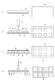
溝形成工程では、上記のスピンドルに溝加工用ダイシングブレード24を装着すると共に、ダイシングテープ22を用いて、X・Y・θ軸テーブルに素子形成側となる表面25を下面としてウェーハ16を貼り付ける(図3(a))。そして、上記のアライメントの後、溝加工用ダイシングブレード24を用いて、スクライブデータに基づく縦分断ラインおよび横分割ラインに倣って非接着部18となる溝を形成する(図3(b))。すなわち、ウェーハ16に対し、各縦分断ラインを中心線として全ての縦溝を研削し、続いてウェーハ16を90°回転した後、各横分割ラインを中心線として全ての横溝を研削する。これにより、上記の非接着部18となる溝が形成される。なお、本実施形態では、非接着部18となる溝の幅は300μm程度であり、その深さは50μm程度である(ウェーハ16の厚さは300μm)。
ここで、非接着部18となる溝が形成されたウェーハ16を表裏反転して、X・Y・θ軸テーブルに再セットするが、その際、ウェーハ16をダイシングテープ22に貼着した状態で、ダイシングテープ22ごと再セットすることが好ましい。すなわち、ウェーハ16を再セットした後、上方から紫外線の照射を行ってダイシングテープ22を剥離することが好ましい。これにより、再セットに伴うハンドリングの際に、ウェーハ16が溝部分でブレイクしてしまうのを防止することができる。もちろん、ウェーハ16が十分に厚い場合には、ダイシングテープ22から剥離した後、再セットを行ってもよい。なお、溝形成が完了した直後に、認識カメラを用いて外観検査を行うことも好ましい。
ダイシング工程では、上記のスピンドルに、溝加工用ダイシングブレード24に代えて分断用ダイシングブレード23を装着すると共に、新たなダイシングテープ22を用いて、X・Y・θ軸テーブルに素子形成側となる表面25を上面としてウェーハ16を貼り付ける(図3(c))。次に、上記のアライメントを行った後、分断用ダイシングブレード23により、スクライブデータに基づく縦分断ラインおよび横分断ラインに倣った分断を行い、ウェーハ16をチップ化する(図3(d))。すなわち、ウェーハ16のブラックマトリクス部分に、各縦分断ラインに沿ってダイシングを行ってウェーハ16を帯状に分断し、続いてウェーハ16を90°回転した後、各横分割ラインに沿ってダイシングを行ってウェーハ16をマトリクス状に分断する。なお、本実施形態では、分断用ダイシングブレード23による分断幅(切り代)は、一般的な30μm程度である。
最後に、認識カメラを用いて外観検査を行うと共に、下側からダイシングテープ22に紫外線を照射して、ダイシングテープ22の粘着力を低減させ、各半導体チップ2を引き剥がし可能な状態とする。ここで、広義のダイシング工程の前に行われた導通検査および上記の外観検査で不良品された半導体チップ2をピックアップし除去して、次工程であるダイボンド工程(一次実装)に移行する。
なお、縦分断ラインまたは横分断ラインのみに倣って、溝形成工程を行うようにして、非接着部18となる溝を形成するようにしてもよい(図4(a)参照)。
また、縦分断ラインおよび/または横分断ラインの中間に相当する位置に、非接着部18となる溝を形成するようにしてもよい(図4(b)参照)。
また、縦分断ラインおよび/または横分断ラインの中間に相当する位置に、非接着部18となる溝を形成するようにしてもよい(図4(b)参照)。
以上の構成によれば、半導体チップの裏面側を簡単な加工で、接着部と非接着部とから成る凹凸形状が形成されているため、チップ支持基板との接触面積が小さくなり、二次実装により生じる半導体チップへの応力を軽減させることができる。
1…半導体装置 2…半導体チップ 3…チップ支持基板 4…ダイボンド材 5…封止材 16…ウェーハ 17…接着部 18…非接着部 23…分断用ダイシングブレード 24…溝加工用ダイシングブレード
Claims (6)
- ダイボンド材を介して、チップ支持基板上に接着固定される半導体チップであって、
前記チップ支持基板に接着固定される前記半導体チップの裏面側が、接着部と非接着部とから成る凹凸形状に形成されていることを特徴とする半導体チップ。 - 前記非接着部は、前記半導体チップの裏面側における4辺の周縁部うち少なくとも一方の平行な2辺の周縁部に形成されていることを特徴とする請求項1に記載の半導体チップ。
- 前記非接着部は、チップ化前のウェーハレベルの状態で、研削により形成した溝であることを特徴とする請求項1または2に記載の半導体チップ。
- 請求項1ないし3のいずれかに記載の半導体チップと、
前記半導体チップを支持する前記チップ支持基板と、
前記半導体チップを前記チップ支持基板に接着固定する前記ダイボンド材と、
前記チップ支持基板上に前記半導体チップを封止する封止材と、を備えたことを特徴とする半導体装置。 - 表面に複数の半導体素子をマトリクス状に作り込んだウェーハを分断して、請求項1に記載の半導体チップの複数個を得る半導体チップの製造方法であって、
分断用ダイシングブレードを用い、ダイシングテープに貼着した前記ウェーハを分断しチップ化するダイシング工程と、
前記ダイシング工程に先立ち、溝加工用ダイシングブレードを用い、表裏反転してダイシングテープに貼着した前記ウェーハに、前記非接着部となる溝を形成する溝形成工程と、を備えたことを特徴とする半導体チップの製造方法。 - 前記ダイシング工程では、縦分断ラインおよび横分断ラインに倣って前記分断が行われ、
前記溝形成工程では、縦分断ラインおよび横分断ラインの少なくとも一方に倣って前記溝が形成されることを特徴とする請求項5に記載の半導体チップの製造方法。
Priority Applications (1)
| Application Number | Priority Date | Filing Date | Title |
|---|---|---|---|
| PCT/JP2011/003169 WO2012168959A1 (ja) | 2011-06-06 | 2011-06-06 | 半導体チップ、これを備えた半導体装置および半導体チップの製造方法 |
Applications Claiming Priority (1)
| Application Number | Priority Date | Filing Date | Title |
|---|---|---|---|
| PCT/JP2011/003169 WO2012168959A1 (ja) | 2011-06-06 | 2011-06-06 | 半導体チップ、これを備えた半導体装置および半導体チップの製造方法 |
Publications (1)
| Publication Number | Publication Date |
|---|---|
| WO2012168959A1 true WO2012168959A1 (ja) | 2012-12-13 |
Family
ID=47295573
Family Applications (1)
| Application Number | Title | Priority Date | Filing Date |
|---|---|---|---|
| PCT/JP2011/003169 Ceased WO2012168959A1 (ja) | 2011-06-06 | 2011-06-06 | 半導体チップ、これを備えた半導体装置および半導体チップの製造方法 |
Country Status (1)
| Country | Link |
|---|---|
| WO (1) | WO2012168959A1 (ja) |
Cited By (1)
| Publication number | Priority date | Publication date | Assignee | Title |
|---|---|---|---|---|
| JP2016072601A (ja) * | 2014-09-29 | 2016-05-09 | パナソニックIpマネジメント株式会社 | 太陽電池の製造方法 |
Citations (2)
| Publication number | Priority date | Publication date | Assignee | Title |
|---|---|---|---|---|
| JPH0278234A (ja) * | 1988-09-14 | 1990-03-19 | Hitachi Ltd | 半導体装置 |
| JP2010021251A (ja) * | 2008-07-09 | 2010-01-28 | Panasonic Corp | 半導体装置及びその製造方法 |
-
2011
- 2011-06-06 WO PCT/JP2011/003169 patent/WO2012168959A1/ja not_active Ceased
Patent Citations (2)
| Publication number | Priority date | Publication date | Assignee | Title |
|---|---|---|---|---|
| JPH0278234A (ja) * | 1988-09-14 | 1990-03-19 | Hitachi Ltd | 半導体装置 |
| JP2010021251A (ja) * | 2008-07-09 | 2010-01-28 | Panasonic Corp | 半導体装置及びその製造方法 |
Cited By (1)
| Publication number | Priority date | Publication date | Assignee | Title |
|---|---|---|---|---|
| JP2016072601A (ja) * | 2014-09-29 | 2016-05-09 | パナソニックIpマネジメント株式会社 | 太陽電池の製造方法 |
Similar Documents
| Publication | Publication Date | Title |
|---|---|---|
| TWI455215B (zh) | 半導體封裝件及其之製造方法 | |
| US9240398B2 (en) | Method for producing image pickup apparatus and method for producing semiconductor apparatus | |
| JP5798834B2 (ja) | 半導体装置の製造方法 | |
| CN104795319B (zh) | 半导体装置及其制造方法 | |
| US10490531B2 (en) | Manufacturing method of semiconductor device and semiconductor device | |
| JP2012146892A (ja) | 半導体装置の製造方法 | |
| US9418907B2 (en) | Method for manufacturing semiconductor device | |
| TWI421956B (zh) | 晶片尺寸封裝件及其製法 | |
| JP5197037B2 (ja) | バンプが形成されたウェーハを処理するウェーハ処理方法 | |
| JP2006190975A (ja) | ウェハレベルパッケージの封止材充填構造、及びその方法 | |
| TW201911477A (zh) | 半導體製程及半導體結構 | |
| JP6482454B2 (ja) | 電子部品の製造方法ならびに電子部品製造装置 | |
| WO2012168959A1 (ja) | 半導体チップ、これを備えた半導体装置および半導体チップの製造方法 | |
| US20070190688A1 (en) | Method for manufacturing semiconductor device with protection layer | |
| JP2007048876A (ja) | 半導体装置の製造方法 | |
| JP2012104644A (ja) | ウェーハ破断方法およびウェーハ破断装置 | |
| CN101924039B (zh) | 半导体封装件及其制造方法 | |
| JP7114176B2 (ja) | 樹脂パッケージ基板の加工方法 | |
| JP4207696B2 (ja) | 半導体パッケージの製造方法 | |
| CN104009052B (zh) | 晶圆封装方法 | |
| WO2007049356A1 (ja) | 半導体装置およびその製造方法 | |
| KR100576886B1 (ko) | 반도체패키지의 제조 방법 | |
| KR100681264B1 (ko) | 전자소자 패키지 및 그의 제조 방법 | |
| JP2005045041A (ja) | 半導体パッケージおよびその製造方法 | |
| JP2011171433A (ja) | 半導体装置の製造方法および半導体装置 |
Legal Events
| Date | Code | Title | Description |
|---|---|---|---|
| 121 | Ep: the epo has been informed by wipo that ep was designated in this application |
Ref document number: 11867304 Country of ref document: EP Kind code of ref document: A1 |
|
| NENP | Non-entry into the national phase |
Ref country code: DE |
|
| 122 | Ep: pct application non-entry in european phase |
Ref document number: 11867304 Country of ref document: EP Kind code of ref document: A1 |
|
| NENP | Non-entry into the national phase |
Ref country code: JP |