WO2012157631A1 - 脂肪族アミン配位セリウム錯体及び該錯体を含む素子 - Google Patents
脂肪族アミン配位セリウム錯体及び該錯体を含む素子 Download PDFInfo
- Publication number
- WO2012157631A1 WO2012157631A1 PCT/JP2012/062375 JP2012062375W WO2012157631A1 WO 2012157631 A1 WO2012157631 A1 WO 2012157631A1 JP 2012062375 W JP2012062375 W JP 2012062375W WO 2012157631 A1 WO2012157631 A1 WO 2012157631A1
- Authority
- WO
- WIPO (PCT)
- Prior art keywords
- group
- layer
- same
- different
- cerium complex
- Prior art date
- Legal status (The legal status is an assumption and is not a legal conclusion. Google has not performed a legal analysis and makes no representation as to the accuracy of the status listed.)
- Ceased
Links
Images

Classifications
-
- C—CHEMISTRY; METALLURGY
- C09—DYES; PAINTS; POLISHES; NATURAL RESINS; ADHESIVES; COMPOSITIONS NOT OTHERWISE PROVIDED FOR; APPLICATIONS OF MATERIALS NOT OTHERWISE PROVIDED FOR
- C09K—MATERIALS FOR MISCELLANEOUS APPLICATIONS, NOT PROVIDED FOR ELSEWHERE
- C09K11/00—Luminescent materials, e.g. electroluminescent or chemiluminescent
- C09K11/06—Luminescent materials, e.g. electroluminescent or chemiluminescent containing organic luminescent materials
-
- C—CHEMISTRY; METALLURGY
- C07—ORGANIC CHEMISTRY
- C07C—ACYCLIC OR CARBOCYCLIC COMPOUNDS
- C07C211/00—Compounds containing amino groups bound to a carbon skeleton
- C07C211/65—Metal complexes of amines
-
- C—CHEMISTRY; METALLURGY
- C07—ORGANIC CHEMISTRY
- C07C—ACYCLIC OR CARBOCYCLIC COMPOUNDS
- C07C309/00—Sulfonic acids; Halides, esters, or anhydrides thereof
- C07C309/01—Sulfonic acids
- C07C309/02—Sulfonic acids having sulfo groups bound to acyclic carbon atoms
- C07C309/03—Sulfonic acids having sulfo groups bound to acyclic carbon atoms of an acyclic saturated carbon skeleton
- C07C309/06—Sulfonic acids having sulfo groups bound to acyclic carbon atoms of an acyclic saturated carbon skeleton containing halogen atoms, or nitro or nitroso groups bound to the carbon skeleton
-
- C—CHEMISTRY; METALLURGY
- C07—ORGANIC CHEMISTRY
- C07D—HETEROCYCLIC COMPOUNDS
- C07D487/00—Heterocyclic compounds containing nitrogen atoms as the only ring hetero atoms in the condensed system, not provided for by groups C07D451/00 - C07D477/00
- C07D487/02—Heterocyclic compounds containing nitrogen atoms as the only ring hetero atoms in the condensed system, not provided for by groups C07D451/00 - C07D477/00 in which the condensed system contains two hetero rings
- C07D487/08—Bridged systems
-
- C—CHEMISTRY; METALLURGY
- C07—ORGANIC CHEMISTRY
- C07F—ACYCLIC, CARBOCYCLIC OR HETEROCYCLIC COMPOUNDS CONTAINING ELEMENTS OTHER THAN CARBON, HYDROGEN, HALOGEN, OXYGEN, NITROGEN, SULFUR, SELENIUM OR TELLURIUM
- C07F5/00—Compounds containing elements of Groups 3 or 13 of the Periodic Table
- C07F5/003—Compounds containing elements of Groups 3 or 13 of the Periodic Table without C-Metal linkages
-
- H—ELECTRICITY
- H10—SEMICONDUCTOR DEVICES; ELECTRIC SOLID-STATE DEVICES NOT OTHERWISE PROVIDED FOR
- H10K—ORGANIC ELECTRIC SOLID-STATE DEVICES
- H10K85/00—Organic materials used in the body or electrodes of devices covered by this subclass
- H10K85/30—Coordination compounds
- H10K85/351—Metal complexes comprising lanthanides or actinides, e.g. comprising europium
-
- C—CHEMISTRY; METALLURGY
- C09—DYES; PAINTS; POLISHES; NATURAL RESINS; ADHESIVES; COMPOSITIONS NOT OTHERWISE PROVIDED FOR; APPLICATIONS OF MATERIALS NOT OTHERWISE PROVIDED FOR
- C09K—MATERIALS FOR MISCELLANEOUS APPLICATIONS, NOT PROVIDED FOR ELSEWHERE
- C09K2211/00—Chemical nature of organic luminescent or tenebrescent compounds
- C09K2211/14—Macromolecular compounds
- C09K2211/1441—Heterocyclic
- C09K2211/1466—Heterocyclic containing nitrogen as the only heteroatom
-
- C—CHEMISTRY; METALLURGY
- C09—DYES; PAINTS; POLISHES; NATURAL RESINS; ADHESIVES; COMPOSITIONS NOT OTHERWISE PROVIDED FOR; APPLICATIONS OF MATERIALS NOT OTHERWISE PROVIDED FOR
- C09K—MATERIALS FOR MISCELLANEOUS APPLICATIONS, NOT PROVIDED FOR ELSEWHERE
- C09K2211/00—Chemical nature of organic luminescent or tenebrescent compounds
- C09K2211/18—Metal complexes
- C09K2211/182—Metal complexes of the rare earth metals, i.e. Sc, Y or lanthanide
-
- H—ELECTRICITY
- H10—SEMICONDUCTOR DEVICES; ELECTRIC SOLID-STATE DEVICES NOT OTHERWISE PROVIDED FOR
- H10K—ORGANIC ELECTRIC SOLID-STATE DEVICES
- H10K2101/00—Properties of the organic materials covered by group H10K85/00
- H10K2101/10—Triplet emission
-
- H—ELECTRICITY
- H10—SEMICONDUCTOR DEVICES; ELECTRIC SOLID-STATE DEVICES NOT OTHERWISE PROVIDED FOR
- H10K—ORGANIC ELECTRIC SOLID-STATE DEVICES
- H10K50/00—Organic light-emitting devices
- H10K50/10—OLEDs or polymer light-emitting diodes [PLED]
- H10K50/11—OLEDs or polymer light-emitting diodes [PLED] characterised by the electroluminescent [EL] layers
Definitions
- the present invention relates to an aliphatic amine coordinated cerium complex and a device containing the complex.
- Non-patent Document 1 a cerium complex having a cyclic ether is useful as a light-emitting material used for manufacturing a light-emitting device such as an organic electroluminescence device.
- cerium complex has a problem in that the maximum emission spectrum (emission peak) is located in the ultraviolet region, making it difficult to use in display applications and illumination applications.
- an object of the present invention is to provide a cerium complex whose emission peak is located in the visible light region and emits light in the visible light region, and further to provide an element that emits light in the visible light region using this complex.
- R 1 , R 2 , R 3 , R 4 and R 5 each independently represent a hydrogen atom or a hydrocarbyl group which may have a substituent.
- B 1 and B 2 each independently represents a hydrocarbondiyl group which may have a substituent.
- a is an integer of 1 or more.
- the plurality of R 1 may be the same or different, and the plurality of B 1 may be the same or different.
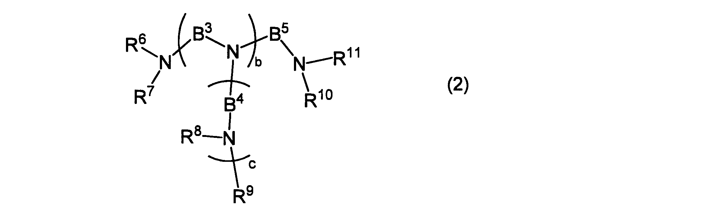
- R 6 , R 7 , R 8 , R 9 , R 10 and R 11 each independently represent a hydrogen atom or a hydrocarbyl group which may have a substituent.
- B 3 , B 4 and B 5 each independently represent a hydrocarbondiyl group which may have a substituent.
- b and c are each independently an integer of 1 or more.
- the plurality of B 3 may be the same or different
- the plurality of B 4 may be the same or different
- the plurality of R 8 may be the same or different.
- the plurality of R 9 may be the same or different, and the plurality of c may be the same or different.
- the plurality of R 8 may be the same or different, and the plurality of B 4 may be the same or different.
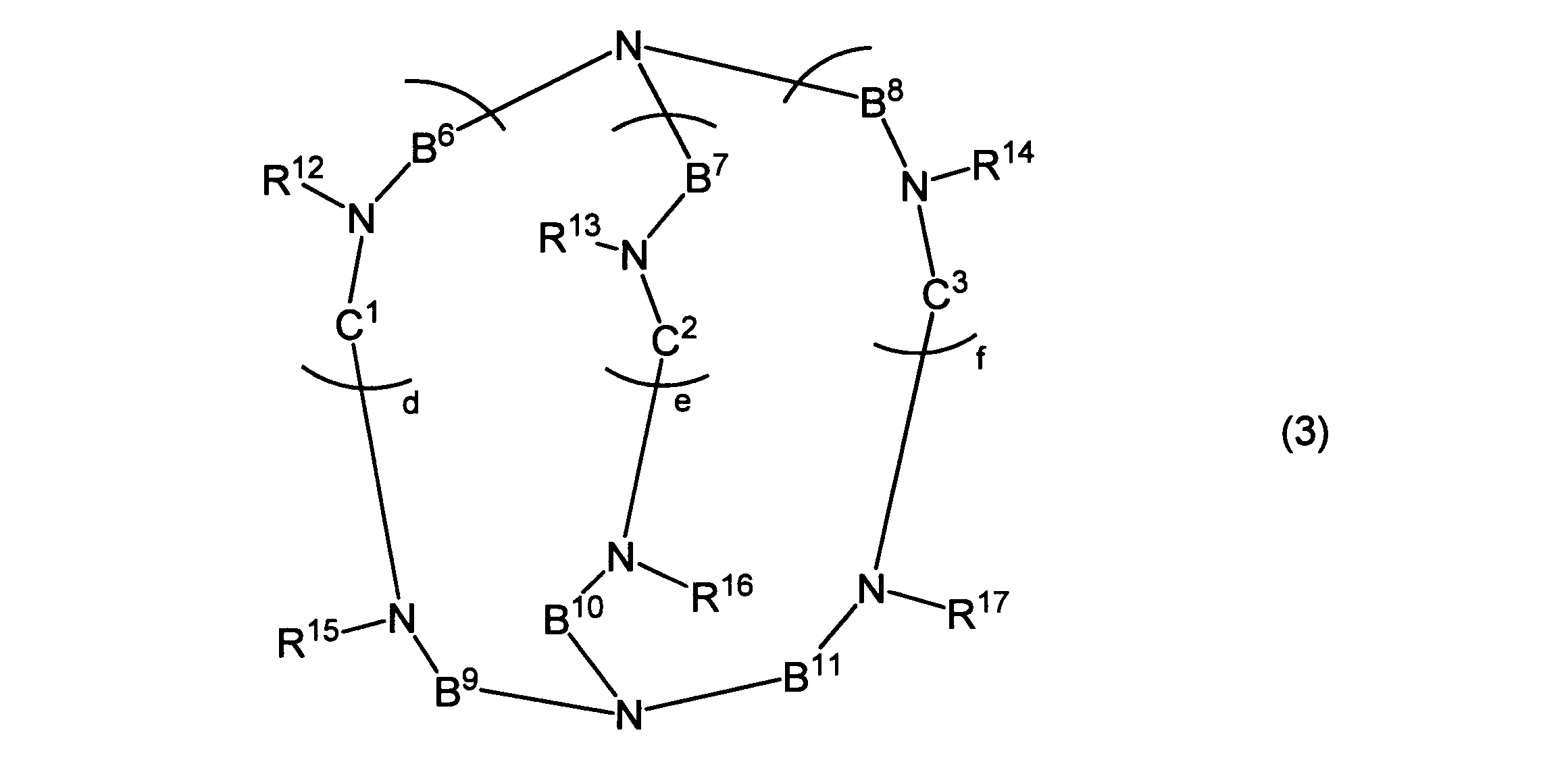
- R 12 , R 13 , R 14 , R 15 , R 16 and R 17 each independently represent a hydrogen atom or a hydrocarbyl group which may have a substituent.
- B 6 , B 7 , B 8 , B 9 , B 10 , B 11 , C 1 , C 2 and C 3 each independently represent a hydrocarbondiyl group which may have a substituent.
- d, e and f are each independently an integer of 1 or more.
- the plurality of R 12 may be the same or different, the plurality of B 6 may be the same or different, and the plurality of C 1 may be the same or different. Also good.
- the plurality of R 13 may be the same or different, the plurality of B 7 may be the same or different, and the plurality of C 2 may be the same or different. Also good.
- the plurality of R 14 may be the same or different, the plurality of B 8 may be the same or different, and the plurality of C 3 may be the same or different. Also good.
- the B 1 , B 2 , B 3 , B 4 , B 5 , B 6 , B 7 , B 8 , B 9 , B 10 and B 11 are ethylene groups which may have a substituent.
- a composition comprising the cerium complex according to [1] or [2] above and a charge transport material.
- a device comprising the cerium complex according to [1] or [2].
- a device comprising the composition according to [3] above.
- [6] The device according to [4] or [5] above, wherein the device is a light emitting device.
- a cerium complex having an emission peak located in the visible light region and emitting light in the visible light region, and further providing an element that emits light in the visible light region using this complex. it can.
- FIG. 1 is a diagram showing an emission spectrum of the cerium complex (D-5) of the present invention in acetonitrile.
- “may have a substituent” means that the hydrogen atom constituting the compound or group described immediately after it is unsubstituted or a part or all of the hydrogen atoms are substituted. Includes both cases where it is substituted. Therefore, in this specification, the “hydrocarbyl group which may have a substituent” means an unsubstituted hydrocarbyl group and a part or all of hydrogen atoms constituting the hydrocarbyl group are substituted with a substituent. Represents both hydrocarbyl groups.
- the “optionally substituted hydrocarbondiyl group” refers to an unsubstituted hydrocarbondiyl group as well as a part or all of the hydrogen atoms constituting the hydrocarbondiyl group substituted by a substituent. Represents a hydrocarbondiyl group.
- substituent is used in the following meaning unless otherwise specified.
- substituent include hydrocarbyl group, hydrocarbyloxy group, hydrocarbylthio group, heterocyclyl group, halogen atom, cyano group, silyl group, substituted silyl group, phosphino group, substituted phosphino group, amino group, substituted amino group, hydroxyl group, And a mercapto group, preferably a hydrocarbyl group, a hydrocarbyloxy group, or a hydrocarbylthio group, and more preferably a hydrocarbyl group.
- the number of carbon atoms of the substituent is usually 1 to 30, preferably 1 to 20, and more preferably. Is 1-10.
- the number of carbon atoms of the substituent is usually 2 to 36, preferably 3 to 26, more preferably 6-16.
- hydrocarbyl group used as a substituent examples include methyl, ethyl, 1-propyl, 2-propyl, 1-butyl, 2-butyl, isobutyl, tert-butyl, pentyl, and hexyl.
- hydrocarbyloxy group used as a substituent examples include methoxy group, ethoxy group, 1-propyloxy group, 2-propyloxy group, 1-butyloxy group, 2-butyloxy group, isobutyloxy group, tert-butyloxy group, Pentyloxy group, hexyloxy group, octyloxy group, decyloxy group, dodecyloxy group, 2-ethylhexyloxy group, 3,7-dimethyloctyloxy group, cyclopropyloxy group, cyclopentyloxy group, cyclohexyloxy group, 1-adamantyl Oxy group, 2-adamantyloxy group, norbornyloxy group, benzyloxy group, ⁇ , ⁇ -dimethylbenzyloxy group, 2-phenethyloxy group, 1-phenethyloxy group, phenoxy group, octylphenoxy group, 1-naphthyl
- hydrocarbylthio group used as a substituent examples include a methylthio group, an ethylthio group, a 1-propylthio group, a 2-propylthio group, a 1-butylthio group, a 2-butylthio group, an isobutylthio group, a tert-butylthio group, and a pentylthio group.
- heterocyclyl group used as a substituent examples include, for example, morpholinyl group, acridinyl group, quinuclidinyl group, tetrahydrofuranyl group, tetrahydropyranyl group, piperazyl group, piperidyl group, benzofuryl group, furyl group, benzothienyl group, thienyl group, benzopyrrolyl.
- the heterocyclyl group means the remaining atomic group excluding one hydrogen atom directly bonded to the carbon atom or nitrogen atom constituting the ring of the heterocyclic compound.
- the substituted silyl group used as a substituent is a silyl group in which 1 to 3 hydrogen atoms in the silyl group are substituted with 1 to 3 hydrocarbyl groups selected from the group consisting of alkyl groups, aryl groups and arylalkyl groups. It is a group.
- the total number of carbon atoms of 1 to 3 hydrocarbyl groups may be determined so that the substituted silyl group as a whole satisfies the above conditions for the number of carbon atoms.
- substituted silyl group examples include trimethylsilyl group, triethylsilyl group, tripropylsilyl group, triisopropylsilyl group, dimethylisopropylsilyl group, diethylisopropylsilyl group, tert-butyldimethylsilyl group, pentyldimethylsilyl group, hexyldimethylsilyl.
- heptyldimethylsilyl group octyldimethylsilyl group, 2-ethylhexyl-dimethylsilyl group, nonyldimethylsilyl group, decyldimethylsilyl group, 3,7-dimethyloctyl-dimethylsilyl group, lauryldimethylsilyl group, triphenylsilyl group , Tri-p-xylylsilyl group, tribenzylsilyl group, diphenylmethylsilyl group, tert-butyldiphenylsilyl group, and dimethylphenylsilyl group, preferably trimethyl Silyl group, triethylsilyl group, or a tri-propyl silyl group.
- substituted phosphino group used as a substituent, one or two hydrogen atoms in the phosphino group are substituted with one or two hydrocarbyl groups selected from the group consisting of an alkyl group, an aryl group and an arylalkyl group. Phosphino group.
- the total number of carbon atoms of one or two hydrocarbyl groups may be determined so that the substituted phosphino group as a whole satisfies the above conditions for the number of carbon atoms.
- Examples of the substituted phosphino group include phenylphosphino group, diphenylphosphino group, methylphosphino group, dimethylphosphino group, ethylphosphino group, diethylphosphino group, propylphosphino group, dipropylphosphino group, butyl Examples thereof include a phosphino group and a dibutylphosphino group, and a diphenylphosphino group, a dimethylphosphino group, a diethylphosphino group, a dipropylphosphino group, or a dibutylphosphino group is preferable.
- one or two hydrogen atoms in the amino group are substituted with one or two hydrocarbyl groups selected from the group consisting of an alkyl group, an aryl group and an arylalkyl group. It is an amino group.
- the total number of carbon atoms of one or two hydrocarbyl groups may be determined so that the substituted amino group as a whole satisfies the above conditions for the number of carbon atoms.
- Examples of the substituted amino group include phenylamino group, diphenylamino group, methylamino group, dimethylamino group, ethylamino group, diethylamino group, propylamino group, dipropylamino group, butylamino group, and dibutylamino group. And preferably a diphenylamino group, a methylamino group, a dimethylamino group, an ethylamino group, a diethylamino group, a dipropylamino group, or a dibutylamino group.
- the cerium ion in the cerium complex of the present invention is usually a trivalent or tetravalent ion, and since the emission intensity is excellent, it is preferably a trivalent ion.
- the cerium complex of the present invention contains a ligand represented by the formula (1).
- A is preferably an integer of 1 to 10, more preferably an integer of 1 to 5, still more preferably an integer of 1 to 3, and particularly preferably 1, because of excellent emission intensity.
- the number of carbon atoms of the hydrocarbyl group represented by R 1 , R 2 , R 3 , R 4 and R 5 is usually 1-30, preferably 1-20, more preferably 1-10. .
- the number of carbon atoms does not include the number of carbon atoms of the substituent.
- Examples of the hydrocarbyl group include methyl group, ethyl group, 1-propyl group, 2-propyl group, 1-butyl group, 2-butyl group, isobutyl group, pentyl group, hexyl group, octyl group, decyl group, dodecyl group.
- R 1 , R 2 , R 3 , R 4 and R 5 may each independently have a hydrogen atom, a methyl group which may have a substituent, or a substituent. It is preferably a good ethyl group, and R 1 , R 2 , R 3 , R 4 and R 5 are all hydrogen atoms, or all may be a methyl group which may have a substituent. More preferred.
- the number of carbon atoms of the hydrocarbondiyl group represented by B 1 and B 2 is usually 1-20, preferably 1-10, more preferably 1 ⁇ 5.
- the number of carbon atoms does not include the number of carbon atoms of the substituent.
- Examples of the hydrocarbon diyl group include methylene group, ethylene group, propylene group, butylene group, pentylene group, hexylene group, octylene group, methylethylene group, methylpropylene group, ethylethylene group, ethylpropylene group, and methylbutylene.
- Group ethylhexylene group, dimethyloctylene group, cyclopropylene group, cyclopentylene group, cyclohexylene group, and adamantanediyl group, preferably methylene group, ethylene group, propylene group, butylene group, or ethyl It is an ethylene group, more preferably a methylene group, an ethylene group, or a propylene group, and still more preferably an ethylene group.
- B 1 and B 2 are each independent, but B 1 and B 2 are preferably the same structure. Since the emission intensity is excellent, it is more preferable that both B 1 and B 2 are ethylene groups which may have a substituent.
- the cerium complex of the present invention contains a ligand represented by the formula (2).
- b has excellent emission intensity, it is preferably an integer of 1 to 10, more preferably an integer of 1 to 5, still more preferably an integer of 1 to 3, and particularly preferably 1.
- c is preferably an integer of 1 to 10, more preferably an integer of 1 to 5, even more preferably an integer of 1 to 3, and particularly preferably 1, because of excellent emission intensity.
- b and c are preferably 1.
- Examples and preferred examples of the hydrocarbyl group represented by R 6 , R 7 , R 8 , R 9 , R 10 and R 11 are the same as the hydrocarbyl group described above for R 1 .
- R 6 , R 7 , R 8 , R 9 , R 10 and R 11 are each independent, but R 6 , R 7 , R 8 , R 9 , R 10 and R 11 are preferably the same structure. Since the emission intensity is excellent, R 6 , R 7 , R 8 , R 9 , R 10 and R 11 are all hydrogen atoms, or all may be a methyl group which may have a substituent. More preferred.
- Examples and preferred examples of the hydrocarbondiyl group represented by B 3 , B 4 and B 5 are the same as the hydrocarbon diyl group described above for B 1 .
- B 3 , B 4 and B 5 are each independent, but B 3 , B 4 and B 5 are preferably the same structure. Since the emission intensity is excellent, it is more preferable that B 3 , B 4 and B 5 are all ethylene groups which may have a substituent.
- the cerium complex of the present invention contains a ligand represented by the formula (3).
- d is preferably an integer of 1 to 10, more preferably an integer of 1 to 5, still more preferably an integer of 1 to 3, and particularly preferably 1, because of excellent emission intensity.
- e is preferably an integer of 1 to 10, more preferably an integer of 1 to 5, even more preferably an integer of 1 to 3, and particularly preferably 1, since the emission intensity is excellent.
- f is preferably an integer of 1 to 10, more preferably an integer of 1 to 5, still more preferably an integer of 1 to 3, and particularly preferably 1, because of excellent emission intensity.
- d, e, and f it is preferable that all of d, e, and f are 1.
- Examples and preferred examples of hydrocarbyl groups represented by R 12 , R 13 , R 14 , R 15 , R 16 and R 17 are the same as the hydrocarbyl groups described above for R 1 .
- R 12 , R 13 , R 14 , R 15 , R 16 and R 17 are each independent, but R 12 , R 13 , R 14 , R 15 , R 16 and R 17 are preferably the same structure. Since the emission intensity is excellent, each of R 12 , R 13 , R 14 , R 15 , R 16 and R 17 may be a hydrogen atom, or may be a methyl group which may have a substituent. More preferred.
- Examples and preferred examples of the hydrocarbon diyl group represented by B 6 , B 7 , B 8 , B 9 , B 10 and B 11 are the same as the hydrocarbon diyl group described above for B 1 .
- B 6 , B 7 , B 8 , B 9 , B 10, and B 11 are each independent, but B 6 , B 7 , B 8 , B 9 , B 10, and B 11 are preferably the same structure. Since the emission intensity is excellent, it is more preferable that B 6 , B 7 , B 8 , B 9 , B 10 and B 11 are all ethylene groups which may have a substituent.
- the number of carbon atoms of the hydrocarbondiyl group represented by C 1 , C 2 and C 3 is usually 1 to 20 and is excellent in emission intensity, and is preferably 1 to 10 and more preferably 1 to 5 It is.
- the number of carbon atoms does not include the number of carbon atoms of the substituent.
- Examples of the hydrocarbon diyl group include methylene group, ethylene group, propylene group, butylene group, pentylene group, hexylene group, octylene group, methylethylene group, methylpropylene group, ethylethylene group, ethylpropylene group, and methylbutylene.
- ethylhexylene group dimethyloctylene group, cyclopropylene group, cyclopentylene group, cyclohexylene group, phenylene group, and adamantanediyl group, preferably methylene group, ethylene group, propylene group, butylene group , Pentylene group, hexylene group, octylene group, methylethylene group, methylpropylene group, ethylethylene group, ethylpropylene group, methylbutylene group, ethylhexylene group, dimethyloctylene group, cyclopropylene group, cyclopentylene group, Cyclo A xylene group or an adamantanediyl group, more preferably a methylene group, an ethylene group, a propylene group, a butylene group or an ethylethylene group, more preferably a methylene group, an ethylene group,
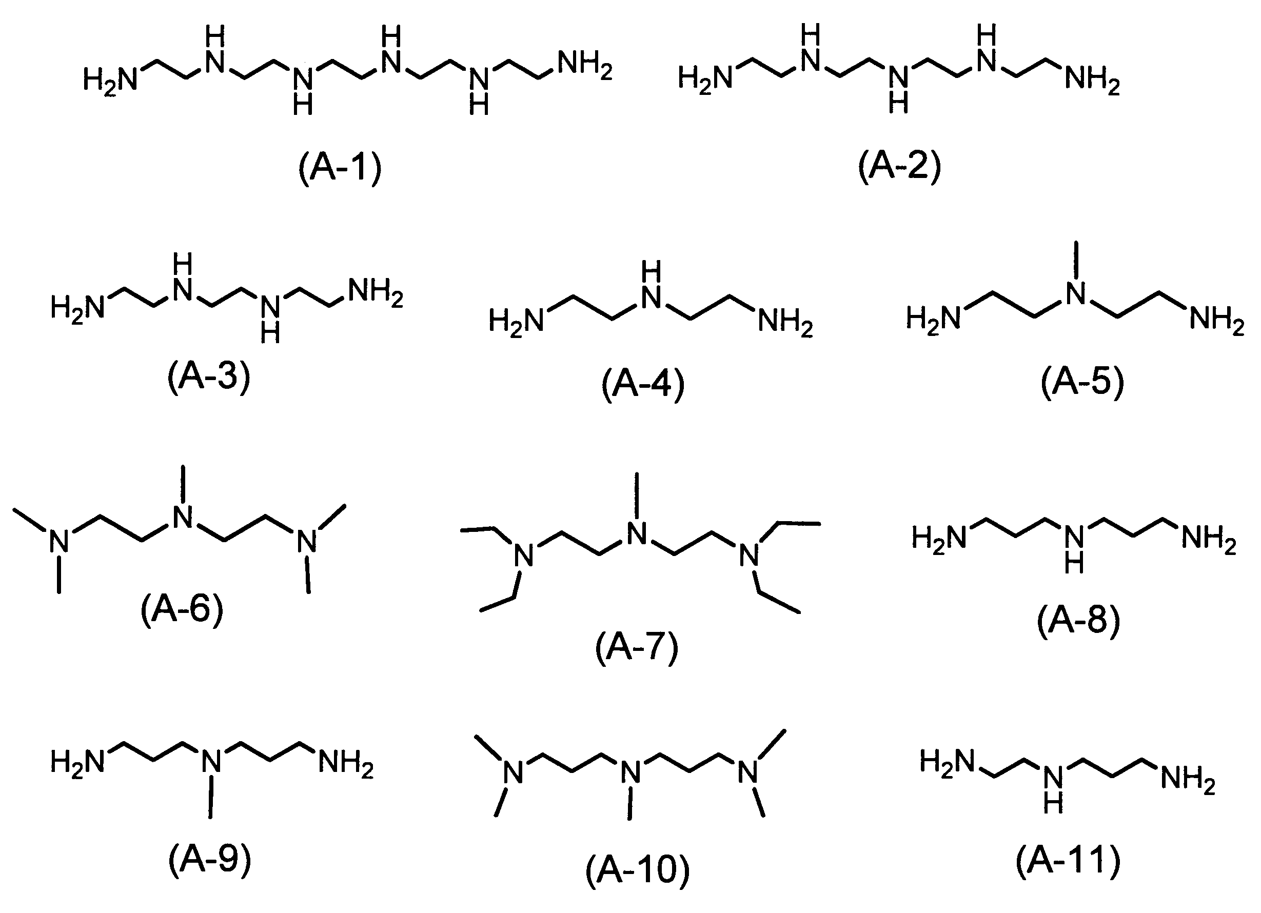
- Examples of the ligand represented by the above formula (1) include the ligands represented by the following formulas (A-1) to (A-11), and the emission intensity is excellent.
- Examples of the ligand represented by the above formula (2) include the ligands represented by the following formulas (B-1) to (B-8), and the emission intensity is excellent.
- Examples of the ligand represented by the above formula (3) include the ligands represented by the following formulas (C-1) to (C-3). It is a ligand represented by the formula (C-2) or (C-3).
- the cerium complex of the present invention is a complex having cerium ions and a ligand represented by any one of the above formulas (1) to (3).
- the ligand represented by any one of the above formulas (1) to (3) may be only one kind, or two or more kinds may be mixed in one complex molecule. Since a stable complex structure can be formed, the cerium complex of the present invention preferably has a ligand represented by the above formula (2) or the above formula (3). It is more preferable to have a ligand represented by:
- the cerium complex of the present invention includes a bidentate or lower (monodentate or bidentate) ligand (L ′) and / or a ligand represented by any one of the above formulas (1) to (3).
- a bidentate or lower (monodentate or bidentate) ligand L ′
- a ligand represented by any one of the above formulas (1) to (3) Alternatively, one or a plurality of counter ions (X) may be contained per one cerium ion.
- the ligand (L ′) is a bidentate or lower ligand different from the ligand represented by any of the above formulas (1) to (3).
- Suitable ligand (L ′) includes, for example, an atomic group containing an atom selected from the group consisting of an oxygen atom, a nitrogen atom and a phosphorus atom, and specific examples include water, methanol, ethanol, acetone, Tetrahydrofuran, dimethyl sulfoxide, triarylphosphine oxide, trialkylphosphine oxide, pyridine, quinoline, pyrazole, imidazole, oxazole, thiazole, benzimidazole, benzoxazole, benzothiazole, triazine, pyrimidine, pyrazine, bipyridine, biquinoline, phenanthroline, triaryl Examples include phosphine, trialkylphosphine, and trialkylamine. There may be only one type of ligand (
- Examples of the counter ion (X) include fluoride ion, chloride ion, bromide ion, iodide ion, sulfate ion, nitrate ion, carbonate ion, acetate ion, perchlorate ion, tetrafluoroborate ion, hexafluorophosphate.
- Ion hexafluoroantimony ion, hexafluoroarsenic ion, methanesulfonic acid ion, trifluoromethanesulfonic acid ion, trifluoroacetic acid ion, benzenesulfonic acid ion, paratoluenesulfonic acid ion, dodecylbenzenesulfonic acid ion, tetraphenylborate ion, And ions such as tetrakis (pentafluorophenyl) borate ion; and polymer compounds containing a repeating unit having at least one ion selected from these ions.
- the ligand (L ′) may be negatively charged, and in this case, the counter ion (X) may be a cation.
- the cation include lithium ion, sodium ion, potassium ion, rubidium ion, cesium ion, and ammonium ion.
- the counter ion (X) may be only one kind or two or more kinds may be mixed in one complex molecule.
- the cerium complex of the present invention preferably has a composition represented by the following composition formula (4).
- M represents a cerium ion
- L represents a ligand represented by any one of the above formulas (1) to (3)
- X represents the counter ion described above
- L ′ represents the above-mentioned Represents a bidentate or lower ligand.
- a ′, b ′ and c ′ are determined by the number of coordination atoms of the ligand and / or the charging ratio at the time of synthesis.
- a ′ is a number of 1 or more, and since the emission intensity is excellent, it is preferably a number of 1 to 4, more preferably 1 or 3. Yes, more preferably 3.
- a ′ is a number of 1 or more, and since the emission intensity is excellent, it is preferably a number of 1 to 4, more preferably 1 or 2. Yes, more preferably 2.
- L is a ligand represented by the above formula (3)
- a ′ is a number of 1 or more, and since the emission intensity is excellent, it is preferably a number of 1 to 4, more preferably 1 or 2. Yes, more preferably 1.
- the plurality of L may be the same or different.
- b ′ is a number of 0 or more, preferably 3 or 4, and more preferably 3.
- c ′ is a number of 0 or more, and since the emission intensity is excellent, it is preferably a number of 0 to 5, more preferably a number of 0 to 2, and further preferably 0 or 1.
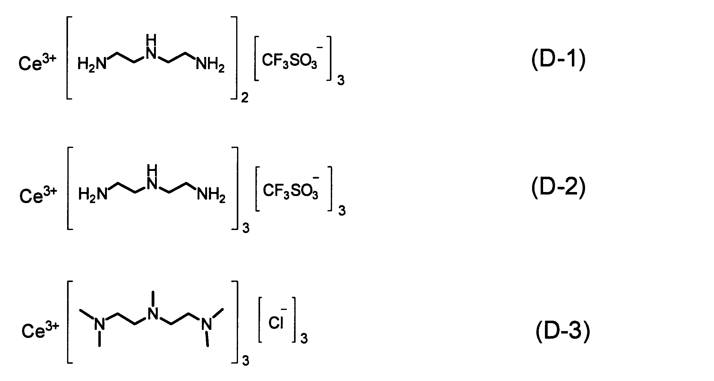
- cerium complex having the composition represented by the composition formula (4) include, for example, cerium having a composition represented by any of the following composition formulas (D-1) to (D-9). Since the emission intensity is excellent, a cerium having a composition represented by any of the following composition formulas (D-2), (D-3), (D-5) to (D-9) is preferable. It is a complex.
- the cerium complex of the present invention may be used alone or in combination of two or more.
- the cerium complex of the present invention as a material for a light-emitting element, an element that emits light in the visible light region can be realized.
- the cerium complex of the present invention is also useful as a magnetic material, a biological probe, a contrast agent, an additive, a modifier, and a catalyst in addition to materials such as a switching element and a photoelectric conversion element.
- cerium complex production method for example, a ligand represented by any one of the above formulas (1) to (3) and a cerium salt are mixed in a solvent at room temperature, and the resulting precipitate is recovered. Or it can manufacture easily by distilling off the solvent of the obtained solution.
- the cerium salt include cerium (III) chloride and cerium (III) trifluoromethanesulfonate.
- Examples of the solvent used when the above-described mixing is performed include an aqueous solvent and an organic solvent, and an organic solvent is preferable.
- organic solvent examples include nitrile solvents such as acetonitrile and benzonitrile; chlorine solvents such as chloroform, methylene chloride, 1,2-dichloroethane, 1,1,2-trichloroethane, chlorobenzene and o-dichlorobenzene; tetrahydrofuran and Ether solvents such as dioxane; aromatic hydrocarbon solvents such as toluene and xylene; such as cyclohexane, methylcyclohexane, n-pentane, n-hexane, n-heptane, n-octane, n-nonane and n-decane Aliphatic hydrocarbon solvents; ketone solvents such as acetone, methyl ethyl ketone and cyclohexanone; ester solvents such as ethyl acetate, butyl acetate and ethyl cellosolve
- composition> The cerium complex of the present invention may be combined with other components to form a composition.
- the composition of the present invention comprises the cerium complex of the present invention and a charge transport material.
- the charge transport material refers to a material that can carry charge in an element such as a light emitting element, and includes a hole transport material and an electron transport material.
- the charge transport material may be any of a low molecular organic compound, a high molecular compound, and an oligomer.
- the polymer compound and the oligomer are preferably conjugated compounds.
- Examples of the hole transport material include known materials used as a hole transport material of a light-emitting element, such as fluorene and derivatives thereof, aromatic amine and derivatives thereof, carbazole derivatives, and polyparaphenylene derivatives.
- Examples of the electron transport material include oxadiazole derivatives, triazine derivatives, anthraquinodimethane and derivatives thereof, benzoquinone and derivatives thereof, naphthoquinone and derivatives thereof, anthraquinone and derivatives thereof, tetracyanoanthraquinodimethane and derivatives thereof, Examples thereof include known materials used as an electron transport material for a light-emitting element, such as a fluorenone derivative, diphenyldicyanoethylene and its derivative, a diphenoquinone derivative, and a metal complex of 8-hydroxyquinoline and its derivative.
- the content of the cerium complex of the present invention in the composition of the present invention is preferably 0.01 to 200 parts by weight, preferably 0.1 to 100 parts by weight with respect to 100 parts by weight of the charge transport material. Is more preferably 1 to 50 parts by weight.
- 1 type or 2 types or more may be sufficient as the cerium complex of this invention contained in the composition of this invention, but it is preferable that it is 1 type.
- the charge transport material contained in the composition of the present invention may be one type or two or more types, but preferably one type.
- the element of the present invention is an element including the cerium complex of the present invention (hereinafter also referred to as “the cerium complex”) or the composition of the present invention (hereinafter also referred to as “the composition”). And an element having a layer containing the cerium complex or the composition between a pair of electrodes including a cathode.
- the element of the present invention is a light-emitting element (hereinafter also referred to as “light-emitting element of the present invention”) will be described.
- the light-emitting element of the present invention has a light-emitting layer between a pair of electrodes including an anode and a cathode.
- the light emitting device of the present invention may contain layers other than the light emitting layer. Examples of the layer other than the light emitting layer include a charge transport layer, a charge injection layer, and a charge blocking layer. Each layer may consist of one layer or two or more layers.
- the cerium complex or the composition is preferably contained in one or more of the above layers.
- the content of the cerium complex or the composition in the layer containing the cerium complex or the composition is usually 0.01 to 100% by weight with respect to the total weight of the layer, and 0.1 to 50%. % By weight is preferred, and 1 to 50% by weight is more preferred.
- it is preferable that the said cerium complex or the said composition is contained in the light emitting layer.
- the light emitting layer is a layer having a function of emitting light.
- the charge transport layer is a layer having a function of transporting holes or electrons. Among them, a layer having a function of transporting holes is called a hole transport layer, and a layer having a function of transporting electrons is transported by electrons. It is called a layer.
- the charge injection layer is a layer having a function of improving the charge injection efficiency from the electrode among the charge transport layers provided adjacent to the electrode and having an effect of lowering the driving voltage of the light emitting element.
- a layer having a function of improving the hole injection efficiency from the cathode is called a hole injection layer, and a layer having a function of improving the electron injection efficiency from the cathode is called an electron injection layer.
- the charge blocking layer is a layer having a function of confining holes or electrons in the light emitting layer, and among them, a layer that transports electrons and confines holes is called a hole blocking layer, and a layer that transports holes and confines electrons. Is called an electron blocking layer.
- a layer that transports electrons and confines holes is called a hole blocking layer
- a layer that transports holes and confines electrons Is called an electron blocking layer.
- these layers may also serve as an electron blocking layer.
- the electron transport layer and / or the electron injection layer have a function of blocking hole transport and confining holes in the light emitting layer, these layers may also serve as a hole blocking layer.
- Examples of the structure of the light emitting device of the present invention include the following structures a) to q). a) anode / light emitting layer / cathode b) anode / hole transport layer / light emitting layer / cathode c) anode / light emitting layer / electron transport layer / cathode d) anode / light emitting layer / hole blocking layer / cathode e) anode / Hole transport layer / light emitting layer / electron transport layer / cathode f) anode / hole injection layer / light emitting layer / cathode g) anode / light emitting layer / electron injection layer / cathode h) anode / hole injection layer / light emitting layer / Electron injection layer / cathode i) anode / hole injection layer / hole transport layer / light emitting layer / cathode j) anode / hole transport
- the light emitting device of the present invention may further include an insulating layer adjacent to the electrode in order to improve adhesion with the electrode or to improve charge injection from the electrode.
- the material used for the insulating layer include metal fluorides, metal oxides, and organic insulating materials.
- the thickness of the insulating layer is usually 2 nm or less.
- a light emitting element provided with an insulating layer the light emitting element provided with the said insulating layer adjacent to a cathode and the light emitting element provided with the said insulating layer adjacent to an anode are mentioned, for example.
- a thin buffer layer may be inserted between adjacent layers in order to improve the adhesion of the interface and prevent mixing. Examples of the buffer layer include a layer containing a conductive polymer compound adjacent to the anode.
- the light-emitting layer can accept holes from the adjacent layer on the anode side when an electric field is applied, and can accept electrons from the adjacent layer on the cathode side, that is, the received charges (ie, electrons and holes).
- the light emitting layer of the light emitting device of the present invention preferably contains the cerium complex or the composition, and preferably contains the cerium complex or the composition as a light emitting material.
- the light emitting layer may contain other light emitting materials.
- luminescent materials include, for example, naphthalene derivatives, anthracene and derivatives thereof, perylene and derivatives thereof, polymethine-based, xanthene-based, coumarin-based, and cyanine-based pigments, metal complexes of 8-hydroxyquinoline and its derivatives, Aromatic amines, tetraphenylcyclopentadiene and its derivatives, and tetraphenylbutadiene and its derivatives are mentioned.
- the light emitting layer may also contain a host material using the cerium complex or the composition as a guest material.
- the host material include a compound having a fluorene skeleton, a compound having a carbazole skeleton, a compound having a diarylamine skeleton, a compound having a pyridine skeleton, a compound having a pyrazine skeleton, a compound having a triazine skeleton, and a compound having an arylsilane skeleton Is mentioned.
- the T1 of the host material (energy level in the lowest triplet excited state) is preferably larger than T1 of the guest material, and more preferably the difference is larger than 0.2 eV.
- the host material may be either a low molecular compound or a high molecular compound.
- the host material and the cerium complex or the composition may be mixed and applied or deposited to form a light-emitting layer in which the cerium complex or the composition is doped in the host material.
- the thickness of the light-emitting layer varies depending on the material used, and may be selected so that the drive voltage and the light emission efficiency are appropriate values.
- the thickness of the light emitting layer is usually 1 nm to 1 ⁇ m, preferably 2 nm to 500 nm, more preferably 5 nm to 200 nm, and still more preferably 50 nm to 150 nm.
- Examples of the material for the hole transport layer include polyvinyl carbazole and derivatives thereof, polysilane and derivatives thereof, polysiloxane derivatives having aromatic amine residues in the side chain or main chain, pyrazoline derivatives, arylamine derivatives, stilbene derivatives, Examples include phenyldiamine derivatives, polyaniline and derivatives thereof, polyaminophen and derivatives thereof, polypyrrole and derivatives thereof, poly (p-phenylene vinylene) and derivatives thereof, and poly (2,5-thienylene vinylene) and derivatives thereof.
- the thickness of the hole transport layer is set so that the light emission efficiency and the driving voltage are appropriate values, and the optimum value varies depending on the material used, but is usually 1 nm to 1 ⁇ m, preferably 2 nm to 500 nm. More preferably, the thickness is 5 nm to 200 nm.
- Examples of the material for the electron transport layer include oxadiazole derivatives, triazine derivatives, anthraquinodimethane and its derivatives, benzoquinone and its derivatives, naphthoquinone and its derivatives, anthraquinone and its derivatives, tetracyanoanthraquinodimethane and its derivatives. , Fluorenone derivatives, diphenyldicyanoethylene and derivatives thereof, diphenoquinone derivatives, metal complexes of 8-hydroxyquinoline and derivatives thereof, polyquinoline and derivatives thereof, polyquinoxaline and derivatives thereof, and polyfluorene and derivatives thereof.
- the thickness of the electron transport layer is set so that the light emission efficiency and the driving voltage are appropriate values, and the optimum value varies depending on the material used, but is usually 1 nm to 1 ⁇ m, preferably 2 nm to 500 nm. More preferably, it is 5 nm to 200 nm.
- Examples of the material for the hole injection layer include conductive polymer oligomers such as aniline copolymers, thiophene oligomers, and polythiophene.
- the thickness of the hole injection layer is set so that the light emission efficiency and the driving voltage have appropriate values, and the optimum value varies depending on the material used, but is usually 1 nm to 1 ⁇ m, preferably 2 nm to 500 nm. More preferably, the thickness is 5 nm to 200 nm.
- the electron injection layer examples include a layer containing a conductive polymer, and a layer containing a material having an ionization potential of an intermediate value between the anode material and the hole transport material contained in the hole transport layer (anode and hole transport). And a layer containing a material having an electron affinity with an intermediate value between the cathode material and the electron transport material contained in the electron transport layer (provided between the cathode and the electron transport layer). Case).
- the material of the electron injection layer may be selected according to the relationship between the material of the electrode and / or the material of the layer adjacent to the electron injection layer.
- the material for the electron injection layer include polyaniline and derivatives thereof, polyaminophen and derivatives thereof, polypyrrole and derivatives thereof, polyphenylene vinylene and derivatives thereof, polythienylene vinylene and derivatives thereof, polyquinoline and derivatives thereof, and polyquinoxaline and derivatives thereof.
- Conductive polymers such as polymers containing an aromatic amine structure in the main chain or side chain, metal phthalocyanines, and carbon.
- the thickness of the electron injection layer is usually 1 nm to 100 nm, preferably 1 nm to 50 nm, more preferably 1 nm to 10 nm.
- Each layer is formed on an adjacent layer or substrate.
- the forming method include a vacuum deposition method (resistance heating deposition method, electron beam method, etc.), sputtering method, LB method, molecular lamination method, and coating method. preferable.
- Examples of the coating method include spin coating, casting, dip coating, gravure coating, bar coating, roll coating, spray coating, screen printing, flexographic printing, offset printing, and inkjet printing.
- a roll coating method, a spray coating method, a flexographic printing method, or an ink jet printing method is preferable.
- the light emitting device of the present invention is usually formed using a substrate.
- An electrode is formed on one surface of the substrate, and further each element layer is formed.
- the substrate include a substrate made of a material such as glass, plastic, or silicon, and a substrate made of a polymer film.
- the anode and the cathode included in the light emitting device of the present invention are transparent or translucent, but the anode is preferably transparent or translucent.
- Examples of the material of the anode include a conductive metal oxide film, a translucent metal thin film, and a transparent organic conductive film.
- a conductive metal oxide film Preferably, indium oxide, zinc oxide, tin oxide, and a composite thereof ( Indium tin oxide (ITO), indium zinc oxide, etc.), antimony tin oxide, NESA, gold, platinum, silver, copper, polyaniline and derivatives thereof, and polyaminophen and derivatives thereof.
- Examples of the method for forming the anode include a vacuum deposition method, a sputtering method, an ion plating method, and a plating method.
- An anode having a laminated structure of two or more layers may be formed.
- the thickness of the anode is set in consideration of light transmittance and electric conductivity, and is usually 10 nm to 10 ⁇ m, preferably 20 nm to 1 ⁇ m, more preferably 40 nm to 500 nm.
- the material of the cathode is preferably a material having a low work function, such as lithium, sodium, potassium, rubidium, cesium, beryllium, magnesium, calcium, strontium, barium, aluminum, scandium, vanadium, zinc, yttrium, indium, cerium, Metals such as samarium, europium, terbium and ytterbium; alloys of two or more metals selected from the group consisting of those metals; one or more metals selected from the group consisting of those metals; and gold, silver, platinum, An alloy with one or more metals selected from the group consisting of copper, manganese, titanium, cobalt, nickel, tungsten, and tin; graphite; a graphite intercalation compound.
- a low work function such as lithium, sodium, potassium, rubidium, cesium, beryllium, magnesium, calcium, strontium, barium, aluminum, scandium, vanadium, zinc, yttrium, indium, ce
- Examples of the method for forming the cathode include a vacuum deposition method, a sputtering method, and a laminating method in which a metal thin film is thermocompression bonded.
- a cathode having a laminated structure of two or more layers may be formed.
- the thickness of the cathode is set in consideration of electric conductivity and durability, and is usually 10 nm to 10 ⁇ m, preferably 20 nm to 1 ⁇ m, more preferably 50 nm to 500 nm.
- a protective layer or a protective cover for protecting the light emitting device may be formed after forming the cathode in order to protect the device from the outside and use it stably for a long time.
- the material used for the protective layer include polymer compounds, metal oxides, metal fluorides, and metal borides.
- the protective cover include a glass plate and a plastic plate having a surface subjected to low water permeability treatment. Among these, it is preferable that the protective cover is bonded to the element using a thermosetting resin or a photocurable resin to seal the element.
- the light emitting element of the present invention is useful for, for example, a planar light source, a segment display device, a dot matrix display device, a backlight of a liquid crystal display device, and illumination.
- the cerium complex of this invention or the composition of this invention can also be used for a photoelectric conversion element.
- the photoelectric conversion element usually has an anode, a cathode, and a charge separation layer.
- the charge separation layer is located between the anode and the cathode.
- the photoelectric conversion element may have an arbitrary layer other than the charge separation layer between the anode and the cathode.
- the metal complex or the composition may be contained in the charge separation layer or in any layer other than the charge separation layer.
- the materials of the cathode and the anode are the same as those described in the section of the light emitting element.
- the shape of the anode and the cathode is not particularly limited, and may be a comb shape.
- the anode and cathode may be either transparent or translucent.
- the charge separation layer of the photoelectric conversion element usually contains an electron donating compound and an electron accepting compound.
- the electron donating compound include a conjugated polymer compound
- examples of the conjugated polymer compound include a conjugated polymer compound containing a thiophenediyl group and a conjugated polymer compound containing a fluorenediyl group.
- an electron-accepting compound a fullerene and a fullerene derivative are mentioned, for example.
- the photoelectric conversion element is usually formed using a substrate.
- substrate is the same as what was demonstrated in the term of the light emitting element.
- the photoelectric conversion element is preferably a solar cell.
- the emission spectrum was measured with a fluorescence spectrophotometer (trade name: FP-6500, manufactured by JASCO Corporation) with an excitation wavelength of 370 nm.
- the reaction of the first step was performed according to US Patent Application Publication No. 2004/267909.
- a 1 L round bottom flask was charged with tris (2-aminoethyl) amine (4.87 g, 33.3 mmol) and 2-propanol (250 mL) and cooled to ⁇ 78 ° C. using an isopropanol / dry ice bath.
- 7.25 g (glyoxal 50 mmol) / 2-propanol (125 mL) of 40 wt% glyoxal aqueous solution was slowly added dropwise (2 drops / second).
- triethylamine (12.5 mL) was added and the temperature was raised to room temperature.
- the resulting reaction solution was dried under reduced pressure at 40 ° C. Chloroform was added to the obtained solid to dissolve it, and then the insoluble solid was filtered off by suction filtration using Celite (filter aid), and the filtrate was dried under reduced pressure at 40 ° C. for 6 hours to obtain an imine compound. 25 g was obtained. Without further purification, it proceeded to the next reaction.
- the second step reaction is described in J.H. Org. Chem. 1993, 58, 7939.
- the imine body (500 mg, 1.39 mmol) obtained in the first step and dehydrated methanol (100 mL) were placed in a 200 mL round bottom flask in which the internal gas was replaced with argon gas, and sodium borohydride (1 (0.00 g, 26.4 mmol) was added, and the mixture was stirred at room temperature for 4.5 hours. A small amount of water was added to the obtained reaction solution, followed by concentration under reduced pressure. Methanol (1 mL) and water (10 mL) were added to the obtained oily liquid and allowed to stand overnight, and then the formed square crystals were removed by filtration.
- a thin film is formed by applying a composition containing cerium complex (D-5) and 1,3-bis (carbazol-9-yl) benzene thereon by spin coating.
- a light emitting element can be manufactured.
Landscapes
- Chemical & Material Sciences (AREA)
- Organic Chemistry (AREA)
- Engineering & Computer Science (AREA)
- Materials Engineering (AREA)
- Inorganic Chemistry (AREA)
- Electroluminescent Light Sources (AREA)
- Materials For Photolithography (AREA)
- Nitrogen Condensed Heterocyclic Rings (AREA)
- Organic Low-Molecular-Weight Compounds And Preparation Thereof (AREA)
Abstract
発光ピークが可視光領域に位置し、可視光領域において発光するセリウム錯体の提供。下記式(1)~(3)のいずれかで表される配位子を有するセリウム錯体。 (式中、R1乃至R17は、それぞれ独立に、水素原子又は置換基を有していてもよいヒドロカルビル基、B1乃至B11、C1乃至C3は、それぞれ独立に、置換基を有していてもよいヒドロカーボンジイル基、a、b、c、d、e及びfは、それぞれ独立に1以上の整数である。)
Description
本発明は、脂肪族アミン配位セリウム錯体及び該錯体を含む素子に関する。
環状エーテルを有するセリウム錯体は、有機エレクトロルミネッセンス素子等の発光素子の作製に用いられる発光材料として有用であることが知られている(非特許文献1)。
T.Yu et al.Solid-State Electronics.51,894-899(2007).
しかし、上述のセリウム錯体では、最大の発光スペクトル(発光ピーク)が紫外光領域に位置し、ディスプレイ用途及び照明用途での利用が困難であるという問題があった。
そこで、本発明の目的は、発光ピークが可視光領域に位置し、可視光領域において発光するセリウム錯体を提供し、更にこの錯体を用いて可視光領域において発光する素子を提供することである。
本発明者らは鋭意検討した結果、下記の構成を有する新規なセリウム錯体により上記課題を解決し得ることを見出し、本発明を完成させるに至った。即ち、本発明は下記の[1]から[6]を提供する。
[1] 下記式(1)~(3)のいずれかで表される配位子を有するセリウム錯体。

(式中、
R1、R2、R3、R4及びR5は、それぞれ独立に、水素原子又は置換基を有していてもよいヒドロカルビル基を表す。
B1及びB2は、それぞれ独立に、置換基を有していてもよいヒドロカーボンジイル基を表す。
aは1以上の整数である。aが2以上であるとき、複数個のR1はそれぞれ同じでも異なっていてもよく、複数個のB1はそれぞれ同じでも異なっていてもよい。)

(式中、
R6、R7、R8、R9、R10及びR11は、それぞれ独立に、水素原子又は置換基を有していてもよいヒドロカルビル基を表す。
B3、B4及びB5は、それぞれ独立に、置換基を有していてもよいヒドロカーボンジイル基を表す。
b及びcは、それぞれ独立に、1以上の整数である。bが2以上であるとき、複数個のB3はそれぞれ同じでも異なっていてもよく、複数個のB4はそれぞれ同じでも異なっていてもよく、複数個のR8はそれぞれ同じでも異なっていてもよく、複数個のR9はそれぞれ同じでも異なっていてもよく、複数個のcはそれぞれ同じでも異なっていてもよい。bが1であり、かつ、cが2以上であるとき、複数個のR8はそれぞれ同じでも異なっていてもよく、複数個のB4はそれぞれ同じでも異なっていてもよい。)
(式中、
R12、R13、R14、R15、R16及びR17は、それぞれ独立に、水素原子又は置換基を有していてもよいヒドロカルビル基を表す。
B6、B7、B8、B9、B10、B11、C1、C2及びC3は、それぞれ独立に、置換基を有していてもよいヒドロカーボンジイル基を表す。
d、e及びfは、それぞれ独立に1以上の整数である。dが2以上であるとき、複数個のR12はそれぞれ同じでも異なっていてもよく、複数個のB6はそれぞれ同じでも異なっていてもよく、複数個のC1はそれぞれ同じでも異なっていてもよい。eが2以上であるとき、複数個のR13はそれぞれ同じでも異なっていてもよく、複数個のB7はそれぞれ同じでも異なっていてもよく、複数個のC2はそれぞれ同じでも異なっていてもよい。fが2以上であるとき、複数個のR14はそれぞれ同じでも異なっていてもよく、複数個のB8はそれぞれ同じでも異なっていてもよく、複数個のC3はそれぞれ同じでも異なっていてもよい。)
[2] 前記B1、B2、B3、B4、B5、B6、B7、B8、B9、B10及びB11が、置換基を有していてもよいエチレン基である上記[1]に記載のセリウム錯体。
[3] 上記[1]又は[2]に記載のセリウム錯体と、電荷輸送材料とを含む組成物。
[4] 上記[1]又は[2]に記載のセリウム錯体を含む素子。
[5] 上記[3]に記載の組成物を含む素子。
[6] 前記素子が発光素子である、上記[4]又は[5]に記載の素子。
[1] 下記式(1)~(3)のいずれかで表される配位子を有するセリウム錯体。
R1、R2、R3、R4及びR5は、それぞれ独立に、水素原子又は置換基を有していてもよいヒドロカルビル基を表す。
B1及びB2は、それぞれ独立に、置換基を有していてもよいヒドロカーボンジイル基を表す。
aは1以上の整数である。aが2以上であるとき、複数個のR1はそれぞれ同じでも異なっていてもよく、複数個のB1はそれぞれ同じでも異なっていてもよい。)
R6、R7、R8、R9、R10及びR11は、それぞれ独立に、水素原子又は置換基を有していてもよいヒドロカルビル基を表す。
B3、B4及びB5は、それぞれ独立に、置換基を有していてもよいヒドロカーボンジイル基を表す。
b及びcは、それぞれ独立に、1以上の整数である。bが2以上であるとき、複数個のB3はそれぞれ同じでも異なっていてもよく、複数個のB4はそれぞれ同じでも異なっていてもよく、複数個のR8はそれぞれ同じでも異なっていてもよく、複数個のR9はそれぞれ同じでも異なっていてもよく、複数個のcはそれぞれ同じでも異なっていてもよい。bが1であり、かつ、cが2以上であるとき、複数個のR8はそれぞれ同じでも異なっていてもよく、複数個のB4はそれぞれ同じでも異なっていてもよい。)
R12、R13、R14、R15、R16及びR17は、それぞれ独立に、水素原子又は置換基を有していてもよいヒドロカルビル基を表す。
B6、B7、B8、B9、B10、B11、C1、C2及びC3は、それぞれ独立に、置換基を有していてもよいヒドロカーボンジイル基を表す。
d、e及びfは、それぞれ独立に1以上の整数である。dが2以上であるとき、複数個のR12はそれぞれ同じでも異なっていてもよく、複数個のB6はそれぞれ同じでも異なっていてもよく、複数個のC1はそれぞれ同じでも異なっていてもよい。eが2以上であるとき、複数個のR13はそれぞれ同じでも異なっていてもよく、複数個のB7はそれぞれ同じでも異なっていてもよく、複数個のC2はそれぞれ同じでも異なっていてもよい。fが2以上であるとき、複数個のR14はそれぞれ同じでも異なっていてもよく、複数個のB8はそれぞれ同じでも異なっていてもよく、複数個のC3はそれぞれ同じでも異なっていてもよい。)
[2] 前記B1、B2、B3、B4、B5、B6、B7、B8、B9、B10及びB11が、置換基を有していてもよいエチレン基である上記[1]に記載のセリウム錯体。
[3] 上記[1]又は[2]に記載のセリウム錯体と、電荷輸送材料とを含む組成物。
[4] 上記[1]又は[2]に記載のセリウム錯体を含む素子。
[5] 上記[3]に記載の組成物を含む素子。
[6] 前記素子が発光素子である、上記[4]又は[5]に記載の素子。
本発明によれば、発光ピークが可視光領域に位置し、可視光領域において発光するセリウム錯体を提供することができ、更に、この錯体を用いて可視光領域において発光する素子を提供することができる。
以下、本発明の実施形態について、説明する。
本明細書において、「置換基を有していてもよい」とは、その直後に記載された化合物又は基を構成する水素原子が無置換の場合及び水素原子の一部又は全部が置換基によって置換されている場合の双方を含む。よって、本明細書において、「置換基を有していてもよいヒドロカルビル基」とは、無置換のヒドロカルビル基、並びにヒドロカルビル基を構成する水素原子の一部又は全部が置換基によって置換されているヒドロカルビル基の双方を表す。同様に、「置換基を有していてもよいヒドロカーボンジイル基」は、無置換のヒドロカーボンジイル基、並びにヒドロカーボンジイル基を構成する水素原子の一部又は全部が置換基によって置換されているヒドロカーボンジイル基を表す。
本明細書において、「置換基」とは、特に説明がない場合、以下の意味で用いられる。
置換基としては、例えば、ヒドロカルビル基、ヒドロカルビルオキシ基、ヒドロカルビルチオ基、ヘテロシクリル基、ハロゲン原子、シアノ基、シリル基、置換シリル基、ホスフィノ基、置換ホスフィノ基、アミノ基、置換アミノ基、水酸基、及びメルカプト基が挙げられ、好ましくは、ヒドロカルビル基、ヒドロカルビルオキシ基、又はヒドロカルビルチオ基であり、より好ましくは、ヒドロカルビル基である。
置換基としては、例えば、ヒドロカルビル基、ヒドロカルビルオキシ基、ヒドロカルビルチオ基、ヘテロシクリル基、ハロゲン原子、シアノ基、シリル基、置換シリル基、ホスフィノ基、置換ホスフィノ基、アミノ基、置換アミノ基、水酸基、及びメルカプト基が挙げられ、好ましくは、ヒドロカルビル基、ヒドロカルビルオキシ基、又はヒドロカルビルチオ基であり、より好ましくは、ヒドロカルビル基である。
上記置換基が、炭素原子を含み、かつ、芳香環を含まない基である場合には、置換基の炭素原子数は、通常、1~30であり、好ましくは1~20であり、より好ましくは1~10である。
上記置換基が、炭素原子を含み、かつ、芳香環を含む基である場合には、置換基の炭素原子数は、通常、2~36であり、好ましくは3~26であり、より好ましくは6~16である。
置換基として用いられるヒドロカルビル基としては、例えば、メチル基、エチル基、1-プロピル基、2-プロピル基、1-ブチル基、2-ブチル基、イソブチル基、tert-ブチル基、ペンチル基、ヘキシル基、オクチル基、デシル基、ドデシル基、2-エチルヘキシル基、3,7-ジメチルオクチル基、シクロプロピル基、シクロペンチル基、シクロヘキシル基、1-アダマンチル基、2-アダマンチル基、ノルボルニル基、ベンジル基、α,α-ジメチルベンジル基、1-フェネチル基、2-フェネチル基、ビニル基、プロペニル基、ブテニル基、オレイル基、エイコサペンタエニル基、ドコサヘキサエニル基、2,2-ジフェニルビニル基、1,2,2-トリフェニルビニル基、2-フェニル-2-プロペニル基、フェニル基、2-トリル基、4-トリル基、2-ビフェニル基、3-ビフェニル基、4-ビフェニル基、ターフェニル基、3,5-ジフェニルフェニル基、3,4-ジフェニルフェニル基、ペンタフェニルフェニル基、4-(2,2-ジフェニルビニル)フェニル基、4-(1,2,2-トリフェニルビニル)フェニル基、フルオレニル基、1-ナフチル基、2-ナフチル基、9-アントリル基、2-アントリル基、9-フェナントリル基、1-ピレニル基、クリセニル基、ナフタセニル基、及びコロニル基が挙げられ、好ましくは、メチル基、エチル基、1-プロピル基、2-プロピル基、1-ブチル基、2-ブチル基、イソブチル基、tert-ブチル基、ペンチル基、ヘキシル基、オクチル基、デシル基、ドデシル基、2-エチルヘキシル基、3,7-ジメチルオクチル基、シクロプロピル基、シクロペンチル基、シクロヘキシル基、1-アダマンチル基、又は2-アダマンチル基であり、より好ましくは、メチル基、エチル基、1-プロピル基、2-プロピル基、1-ブチル基、2-ブチル基、イソブチル基、tert-ブチル基、ペンチル基、ヘキシル基、オクチル基、デシル基、ドデシル基、2-エチルヘキシル基、又は3,7-ジメチルオクチル基である。
置換基として用いられるヒドロカルビルオキシ基としては、例えば、メトキシ基、エトキシ基、1-プロピルオキシ基、2-プロピルオキシ基、1-ブチルオキシ基、2-ブチルオキシ基、イソブチルオキシ基、tert-ブチルオキシ基、ペンチルオキシ基、ヘキシルオキシ基、オクチルオキシ基、デシルオキシ基、ドデシルオキシ基、2-エチルヘキシルオキシ基、3,7-ジメチルオクチルオキシ基、シクロプロピルオキシ基、シクロペンチルオキシ基、シクロヘキシルオキシ基、1-アダマンチルオキシ基、2-アダマンチルオキシ基、ノルボルニルオキシ基、ベンジルオキシ基、α,α-ジメチルベンジロキシ基、2-フェネチルオキシ基、1-フェネチルオキシ基、フェノキシ基、オクチルフェノキシ基、1-ナフチルオキシ基、及び2-ナフチルオキシ基が挙げられ、好ましくは、メトキシ基、エトキシ基、1-プロピルオキシ基、2-プロピルオキシ基、1-ブチルオキシ基、2-ブチルオキシ基、イソブチルオキシ基、tert-ブチルオキシ基、ペンチルオキシ基、ヘキシルオキシ基、オクチルオキシ基、デシルオキシ基、ドデシルオキシ基、2-エチルヘキシルオキシ基、又は3,7-ジメチルオクチルオキシ基であり、より好ましくは、メトキシ基、エトキシ基、又は1-プロピルオキシ基である。
置換基として用いられるヒドロカルビルチオ基としては、例えば、メチルチオ基、エチルチオ基、1-プロピルチオ基、2-プロピルチオ基、1-ブチルチオ基、2-ブチルチオ基、イソブチルチオ基、tert-ブチルチオ基、ペンチルチオ基、ヘキシルチオ基、オクチルチオ基、デシルチオ基、ドデシルチオ基、2-エチルヘキシルチオ基、3,7-ジメチルオクチルチオ基、シクロプロピルチオ基、シクロペンチルチオ基、シクロヘキシルチオ基、1-アダマンチルチオ基、2-アダマンチルチオ基、ノルボルニルチオ基、ベンジルチオ基、α,α-ジメチルベンジルチオ基、2-フェネチルチオ基、1-フェネチルチオ基、フェニルチオ基、メトキシフェニルチオ基、オクチルフェニルチオ基、1-ナフチルチオ基、及び2-ナフチルチオ基が挙げられ、好ましくは、メチルチオ基、エチルチオ基、1-プロピルチオ基、2-プロピルチオ基、1-ブチルチオ基、2-ブチルチオ基、イソブチルチオ基、ペンチルチオ基、ヘキシルチオ基、オクチルチオ基、デシルチオ基、ドデシルチオ基、2-エチルヘキシルチオ基、又は3,7-ジメチルオクチルチオ基であり、より好ましくは、メチルチオ基、エチルチオ基、又は1-プロピルチオ基である。
置換基として用いられるヘテロシクリル基としては、例えば、モルホリニル基、アクリジニル基、キヌクリジニル基、テトラヒドロフラニル基、テトラヒドロピラニル基、ピペラジル基、ピペリジル基、ベンゾフリル基、フリル基、ベンゾチエニル基、チエニル基、ベンゾピロリル基、ピロリル基、キノリル基、及びピリジル基が挙げられ、好ましくは、モルホリニル基、アクリジニル基、キヌクリジニル基、テトラヒドロフラニル基、テトラヒドロピラニル基、ピペラジル基、又はピペリジル基である。
なお、ヘテロシクリル基とは、複素環式化合物の環を構成する炭素原子または窒素原子に直接結合する水素原子1個を除いた残りの原子団を意味する。
なお、ヘテロシクリル基とは、複素環式化合物の環を構成する炭素原子または窒素原子に直接結合する水素原子1個を除いた残りの原子団を意味する。
置換基として用いられるハロゲン原子としては、フッ素原子、塩素原子、臭素原子、及びヨウ素原子が挙げられ、好ましくは、フッ素原子、又は塩素原子である。
置換基として用いられる置換シリル基は、シリル基における水素原子の1~3個が、アルキル基、アリール基及びアリールアルキル基からなる群から選ばれる1~3個のヒドロカルビル基で置換されているシリル基である。なお、置換シリル基において、1~3個のヒドロカルビル基の炭素原子数の合計は、置換シリル基が全体として上述の炭素原子数の条件を満たすように決定してよい。
置換シリル基としては、例えば、トリメチルシリル基、トリエチルシリル基、トリプロピルシリル基、トリイソプロピルシリル基、ジメチルイソプロピルシリル基、ジエチルイソプロピルシリル基、tert-ブチルジメチルシリル基、ペンチルジメチルシリル基、ヘキシルジメチルシリル基、ヘプチルジメチルシリル基、オクチルジメチルシリル基、2-エチルヘキシル-ジメチルシリル基、ノニルジメチルシリル基、デシルジメチルシリル基、3,7-ジメチルオクチル-ジメチルシリル基、ラウリルジメチルシリル基、トリフェニルシリル基、トリ-p-キシリルシリル基、トリベンジルシリル基、ジフェニルメチルシリル基、tert-ブチルジフェニルシリル基、及びジメチルフェニルシリル基が挙げられ、好ましくは、トリメチルシリル基、トリエチルシリル基、又はトリプロピルシリル基である。
置換シリル基としては、例えば、トリメチルシリル基、トリエチルシリル基、トリプロピルシリル基、トリイソプロピルシリル基、ジメチルイソプロピルシリル基、ジエチルイソプロピルシリル基、tert-ブチルジメチルシリル基、ペンチルジメチルシリル基、ヘキシルジメチルシリル基、ヘプチルジメチルシリル基、オクチルジメチルシリル基、2-エチルヘキシル-ジメチルシリル基、ノニルジメチルシリル基、デシルジメチルシリル基、3,7-ジメチルオクチル-ジメチルシリル基、ラウリルジメチルシリル基、トリフェニルシリル基、トリ-p-キシリルシリル基、トリベンジルシリル基、ジフェニルメチルシリル基、tert-ブチルジフェニルシリル基、及びジメチルフェニルシリル基が挙げられ、好ましくは、トリメチルシリル基、トリエチルシリル基、又はトリプロピルシリル基である。
置換基として用いられる、置換ホスフィノ基は、ホスフィノ基における水素原子の1個又は2個が、アルキル基、アリール基及びアリールアルキル基からなる群から選ばれる1個又は2個のヒドロカルビル基で置換されているホスフィノ基である。なお、置換ホスフィノ基において、1個又は2個のヒドロカルビル基の炭素原子数の合計は、置換ホスフィノ基が全体として上述の炭素原子数の条件を満たすように決定してよい。
置換ホスフィノ基としては、例えば、フェニルホスフィノ基、ジフェニルホスフィノ基、メチルホスフィノ基、ジメチルホスフィノ基、エチルホスフィノ基、ジエチルホスフィノ基、プロピルホスフィノ基、ジプロピルホスフィノ基、ブチルホスフィノ基、及びジブチルホスフィノ基が挙げられ、好ましくは、ジフェニルホスフィノ基、ジメチルホスフィノ基、ジエチルホスフィノ基、ジプロピルホスフィノ基、又はジブチルホスフィノ基である。
置換ホスフィノ基としては、例えば、フェニルホスフィノ基、ジフェニルホスフィノ基、メチルホスフィノ基、ジメチルホスフィノ基、エチルホスフィノ基、ジエチルホスフィノ基、プロピルホスフィノ基、ジプロピルホスフィノ基、ブチルホスフィノ基、及びジブチルホスフィノ基が挙げられ、好ましくは、ジフェニルホスフィノ基、ジメチルホスフィノ基、ジエチルホスフィノ基、ジプロピルホスフィノ基、又はジブチルホスフィノ基である。
置換基として用いられる、置換アミノ基は、アミノ基における水素原子の1個又は2個が、アルキル基、アリール基及びアリールアルキル基からなる群から選ばれる1個又は2個のヒドロカルビル基で置換されているアミノ基である。なお、置換アミノ基において、1個又は2個のヒドロカルビル基の炭素原子数の合計は、置換アミノ基が全体として上述の炭素原子数の条件を満たすように決定してよい。
置換アミノ基としては、例えば、フェニルアミノ基、ジフェニルアミノ基、メチルアミノ基、ジメチルアミノ基、エチルアミノ基、ジエチルアミノ基、プロピルアミノ基、ジプロピルアミノ基、ブチルアミノ基、及びジブチルアミノ基が挙げられ、好ましくは、ジフェニルアミノ基、メチルアミノ基、ジメチルアミノ基、エチルアミノ基、ジエチルアミノ基、ジプロピルアミノ基、又はジブチルアミノ基である。
置換アミノ基としては、例えば、フェニルアミノ基、ジフェニルアミノ基、メチルアミノ基、ジメチルアミノ基、エチルアミノ基、ジエチルアミノ基、プロピルアミノ基、ジプロピルアミノ基、ブチルアミノ基、及びジブチルアミノ基が挙げられ、好ましくは、ジフェニルアミノ基、メチルアミノ基、ジメチルアミノ基、エチルアミノ基、ジエチルアミノ基、ジプロピルアミノ基、又はジブチルアミノ基である。
<セリウム錯体>
本発明のセリウム錯体における、セリウムイオンは、通常、3価又は4価のイオンであり、発光強度が優れるので、3価のイオンであることが好ましい。
本発明のセリウム錯体における、セリウムイオンは、通常、3価又は4価のイオンであり、発光強度が優れるので、3価のイオンであることが好ましい。
一実施形態では、本発明のセリウム錯体は前記式(1)で表される配位子を含む。
aは、発光強度が優れるので、好ましくは1~10の整数であり、より好ましくは1~5の整数であり、更に好ましくは1~3の整数であり、特に好ましくは1である。
R1、R2、R3、R4及びR5で表されるヒドロカルビル基の炭素原子数は、通常、1~30であり、好ましくは1~20であり、より好ましくは1~10である。該炭素原子数には置換基の炭素原子数は含まれない。該ヒドロカルビル基としては、例えば、メチル基、エチル基、1-プロピル基、2-プロピル基、1-ブチル基、2-ブチル基、イソブチル基、ペンチル基、ヘキシル基、オクチル基、デシル基、ドデシル基、2-エチルヘキシル基、3,7-ジメチルオクチル基、シクロプロピル基、シクロペンチル基、シクロヘキシル基、フェニル基、1-アダマンチル基、及び2-アダマンチル基が挙げられ、好ましくは、メチル基、エチル基、1-プロピル基、2-プロピル基、1-ブチル基、2-ブチル基、イソブチル基、ペンチル基、ヘキシル基、オクチル基、デシル基、ドデシル基、2-エチルヘキシル基、3,7-ジメチルオクチル基、シクロプロピル基、シクロペンチル基、シクロヘキシル基、1-アダマンチル基、又は2-アダマンチル基であり、より好ましくは、メチル基、エチル基、1-プロピル基、2-プロピル基、1-ブチル基、2-ブチル基、イソブチル基、ペンチル基、ヘキシル基、又はオクチル基である。
発光強度が優れるので、R1、R2、R3、R4及びR5は、それぞれ独立に、水素原子、置換基を有していてもよいメチル基、又は置換基を有していてもよいエチル基であることが好ましく、R1、R2、R3、R4及びR5は何れも水素原子であるか、又は何れも置換基を有していてもよいメチル基であることがより好ましい。
B1及びB2で表されるヒドロカーボンジイル基(「ヒドロカルビレン基」ともいわれる。)の炭素原子数は、通常、1~20であり、好ましくは1~10であり、より好ましくは1~5である。該炭素原子数には置換基の炭素原子数は含まれない。該ヒドロカーボンジイル基としては、例えば、メチレン基、エチレン基、プロピレン基、ブチレン基、ペンチレン基、へキシレン基、オクチレン基、メチルエチレン基、メチルプロピレン基、エチルエチレン基、エチルプロピレン基、メチルブチレン基、エチルヘキシレン基、ジメチルオクチレン基、シクロプロピレン基、シクロペンチレン基、シクロヘキシレン基、及びアダマンタンジイル基が挙げられ、好ましくは、メチレン基、エチレン基、プロピレン基、ブチレン基、又はエチルエチレン基であり、より好ましくは、メチレン基、エチレン基、又はプロピレン基であり、更に好ましくは、エチレン基である。
B1とB2はそれぞれ独立であるが、B1とB2は同じ構造であることが好ましい。発光強度が優れるので、B1とB2は何れも置換基を有していてもよいエチレン基であることがより好ましい。
一実施形態では、本発明のセリウム錯体は前記式(2)で表される配位子を含む。
bは、発光強度が優れるので、好ましくは1~10の整数であり、より好ましくは1~5の整数であり、更に好ましくは1~3の整数であり、特に好ましくは1である。
cは、発光強度が優れるので、好ましくは1~10の整数であり、より好ましくは1~5の整数であり、更に好ましくは1~3の整数であり、特に好ましくは1である。
cは、発光強度が優れるので、好ましくは1~10の整数であり、より好ましくは1~5の整数であり、更に好ましくは1~3の整数であり、特に好ましくは1である。
bとcの組み合わせとしては、bとcが1であることが好ましい。
R6、R7、R8、R9、R10及びR11で表されるヒドロカルビル基の例及び好ましい例は、R1で上述したヒドロカルビル基と同じである。
R6、R7、R8、R9、R10及びR11はそれぞれ独立であるが、R6、R7、R8、R9、R10及びR11は同じ構造であることが好ましい。発光強度が優れるので、R6、R7、R8、R9、R10及びR11は何れも水素原子であるか、又は何れも置換基を有していてもよいメチル基であることがより好ましい。
B3、B4及びB5で表されるヒドロカーボンジイル基の例及び好ましい例は、B1で上述したヒドロカーボンジイル基と同じである。
B3、B4及びB5はそれぞれ独立であるが、B3、B4及びB5は同じ構造であることが好ましい。発光強度が優れるので、B3、B4及びB5は何れも置換基を有していてもよいエチレン基であることがより好ましい。
一実施形態では、本発明のセリウム錯体は前記式(3)で表される配位子を含む。
dは、発光強度が優れるので、好ましくは1~10の整数であり、より好ましくは1~5の整数であり、更に好ましくは1~3の整数であり、特に好ましくは1である。
eは、発光強度が優れるので、好ましくは1~10の整数であり、より好ましくは1~5の整数であり、更に好ましくは1~3の整数であり、特に好ましくは1である。
fは、発光強度が優れるので、好ましくは1~10の整数であり、より好ましくは1~5の整数であり、更に好ましくは1~3の整数であり、特に好ましくは1である。
eは、発光強度が優れるので、好ましくは1~10の整数であり、より好ましくは1~5の整数であり、更に好ましくは1~3の整数であり、特に好ましくは1である。
fは、発光強度が優れるので、好ましくは1~10の整数であり、より好ましくは1~5の整数であり、更に好ましくは1~3の整数であり、特に好ましくは1である。
d、e、及びfの組み合わせとしては、d、e、及びfのいずれもが1であることが好ましい。
R12、R13、R14、R15、R16及びR17で表されるヒドロカルビル基の例及び好ましい例は、R1で上述したヒドロカルビル基と同じである。
R12、R13、R14、R15、R16及びR17はそれぞれ独立であるが、R12、R13、R14、R15、R16及びR17は同じ構造であることが好ましい。発光強度が優れるので、R12、R13、R14、R15、R16及びR17は何れも水素原子であるか、又は何れも置換基を有していてもよいメチル基であることがより好ましい。
B6、B7、B8、B9、B10及びB11で表されるヒドロカーボンジイル基の例及び好ましい例は、B1で上述したヒドロカーボンジイル基と同じである。
B6、B7、B8、B9、B10及びB11はそれぞれ独立であるが、B6、B7、B8、B9、B10及びB11は同じ構造であることが好ましい。発光強度が優れるので、B6、B7、B8、B9、B10及びB11は何れも置換基を有していてもよいエチレン基であることがより好ましい。
C1、C2及びC3で表されるヒドロカーボンジイル基の炭素原子数は、通常、1~20であり、発光強度が優れるので、好ましくは1~10であり、より好ましくは1~5である。該炭素原子数には置換基の炭素原子数は含まれない。該ヒドロカーボンジイル基としては、例えば、メチレン基、エチレン基、プロピレン基、ブチレン基、ペンチレン基、へキシレン基、オクチレン基、メチルエチレン基、メチルプロピレン基、エチルエチレン基、エチルプロピレン基、メチルブチレン基、エチルヘキシレン基、ジメチルオクチレン基、シクロプロピレン基、シクロペンチレン基、シクロヘキシレン基、フェニレン基、及びアダマンタンジイル基が挙げられ、好ましくは、メチレン基、エチレン基、プロピレン基、ブチレン基、ペンチレン基、へキシレン基、オクチレン基、メチルエチレン基、メチルプロピレン基、エチルエチレン基、エチルプロピレン基、メチルブチレン基、エチルヘキシレン基、ジメチルオクチレン基、シクロプロピレン基、シクロペンチレン基、シクロヘキシレン基、又はアダマンタンジイル基であり、より好ましくは、メチレン基、エチレン基、プロピレン基、ブチレン基、又はエチルエチレン基であり、より好ましくは、メチレン基、エチレン基、又はプロピレン基であり、更に好ましくは、エチレン基である。
上記式(1)で表される配位子としては、例えば、下記式(A-1)~(A-11)で表される配位子が挙げられ、発光強度が優れるので、好ましくは下記式(A-4)~(A-11)で表される配位子であり、より好ましくは下記式(A-4)~(A-7)で表される配位子である。
上記式(2)で表される配位子としては、例えば、下記式(B-1)~(B-8)で表される配位子が挙げられ、発光強度が優れるので、好ましくは下記式(B-6)~(B-8)で表される配位子であり、より好ましくは下記式(B-6)又は(B-7)で表される配位子である。

上記式(3)で表される配位子としては、例えば、下記式(C-1)~(C-3)で表される配位子が挙げられ、発光強度が優れるので、好ましくは下記式(C-2)又は(C-3)で表される配位子である。

本発明のセリウム錯体は、セリウムイオンと、上記式(1)~(3)のいずれかで表される配位子とを有する錯体である。なお、上記式(1)~(3)のいずれかで表される配位子は、1種のみであっても、2種以上を1錯体分子中に混在させてもよい。安定な錯体構造を形成することができるので、本発明のセリウム錯体は、上記式(2)又は上記式(3)で表される配位子を有していることが好ましく、上記式(3)で表される配位子を有していることがより好ましい。
本発明のセリウム錯体は、上記式(1)~(3)のいずれかで表される配位子の他に、2座以下(1座又は2座)の配位子(L’)及び/又は対イオン(X)を、セリウムイオン1個に対し、1個若しくは複数個含有していてもよい。
配位子(L’)は、上記式(1)~(3)のいずれかで表される配位子とは異なる2座以下の配位子である。好適な配位子(L’)としては、例えば、酸素原子、窒素原子及びリン原子からなる群から選ばれる原子を含む原子団が挙げられ、具体例としては、水、メタノール、エタノール、アセトン、テトラヒドロフラン、ジメチルスルホキシド、トリアリールホスフィンオキシド、トリアルキルホスフィンオキシド、ピリジン、キノリン、ピラゾール、イミダゾール、オキサゾール、チアゾール、ベンゾイミダゾール、ベンゾオキサゾール、ベンゾチアゾール、トリアジン、ピリミジン、ピラジン、ビピリジン、ビキノリン、フェナントロリン、トリアリールホスフィン、トリアルキルホスフィン、及びトリアルキルアミンが挙げられる。配位子(L’)は、1種のみであっても、2種以上を1錯体分子中に混在させてもよい。
対イオン(X)としては、例えば、フッ化物イオン、塩化物イオン、臭化物イオン、ヨウ化物イオン、硫酸イオン、硝酸イオン、炭酸イオン、酢酸イオン、過塩素酸イオン、テトラフルオロボレートイオン、ヘキサフルオロホスフェートイオン、ヘキサフルオロアンチモンイオン、ヘキサフルオロヒ素イオン、メタンスルホン酸イオン、トリフルオロメタンスルホン酸イオン、トリフルオロ酢酸イオン、ベンゼンスルホン酸イオン、パラトルエンスルホン酸イオン、ドデシルベンゼンスルホン酸イオン、テトラフェニルボレートイオン、及びテトラキス(ペンタフルオロフェニル)ボレートイオン等のイオン;これらのイオンから選ばれる少なくとも1つのイオンを有する繰り返し単位を含む高分子化合物が挙げられる。配位子(L’)はマイナスに帯電していてもよく、その場合、対イオン(X)はカチオンであってもよい。カチオンとしては、例えば、リチウムイオン、ナトリウムイオン、カリウムイオン、ルビジウムイオン、セシウムイオン、及びアンモニウムイオンが挙げられる。対イオン(X)は、1種のみであっても、2種以上を1錯体分子中に混在させてもよい。
本発明のセリウム錯体は、下記組成式(4)で表される組成を有することが好ましい。

式(4)において、Mはセリウムイオンを表し、Lは上記式(1)~(3)のいずれかで表される配位子を表し、Xは上述した対イオンを表し、L’は上述した2座以下の配位子を表す。
式(4)において、a’、b’及びc’は、配位子の配位原子数及び/又は合成時の仕込み比によって決まる。
Lが上記式(1)で表される配位子のとき、a’は1以上の数であり、発光強度が優れるので、好ましくは1~4の数であり、より好ましくは1又は3であり、更に好ましくは3である。
Lが上記式(2)で表される配位子のとき、a’は1以上の数であり、発光強度が優れるので、好ましくは1~4の数であり、より好ましくは1又は2であり、更に好ましくは2である。
Lが上記式(3)で表される配位子のとき、a’は1以上の数であり、発光強度が優れるので、好ましくは1~4の数であり、より好ましくは1又は2であり、更に好ましくは1である。
a’が2以上のとき、複数個のLはそれぞれ同じでも異なっていてもよい。
b’は0以上の数であり、好ましくは、3又は4であり、より好ましくは3である。
c’は0以上の数であり、発光強度が優れるので、好ましくは0~5の数であり、より好ましくは0~2の数であり、更に好ましくは0又は1である。
Lが上記式(2)で表される配位子のとき、a’は1以上の数であり、発光強度が優れるので、好ましくは1~4の数であり、より好ましくは1又は2であり、更に好ましくは2である。
Lが上記式(3)で表される配位子のとき、a’は1以上の数であり、発光強度が優れるので、好ましくは1~4の数であり、より好ましくは1又は2であり、更に好ましくは1である。
a’が2以上のとき、複数個のLはそれぞれ同じでも異なっていてもよい。
b’は0以上の数であり、好ましくは、3又は4であり、より好ましくは3である。
c’は0以上の数であり、発光強度が優れるので、好ましくは0~5の数であり、より好ましくは0~2の数であり、更に好ましくは0又は1である。
前記組成式(4)で表される組成を有するセリウム錯体としては、具体的には、例えば、下記組成式(D-1)~(D-9)のいずれかで表される組成を有するセリウム錯体が挙げられ、発光強度が優れるので、好ましくは下記組成式(D-2)、(D-3)、(D-5)~(D-9)のいずれかで表される組成を有するセリウム錯体である。


本発明のセリウム錯体は、1種単独で用いても2種以上を併用してもよい。本発明のセリウム錯体は、発光素子の材料として用いることにより、可視光領域において発光する素子を実現することができる。本発明のセリウム錯体はまた、スイッチング素子、光電変換素子等の材料のほか、磁気材料、生体プローブ、造影剤、添加剤、改質剤、触媒としても有用である。
-セリウム錯体の製造方法-
本発明のセリウム錯体は、例えば、上記式(1)~(3)のいずれかで表される配位子とセリウム塩とを、室温下、溶媒中で混合させ、得られた沈殿を回収するか又は得られた溶液の溶媒を留去することで、容易に製造することができる。上記セリウム塩としては、例えば、塩化セリウム(III)、及びトリフルオロメタンスルホン酸セリウム(III)が挙げられる。
本発明のセリウム錯体は、例えば、上記式(1)~(3)のいずれかで表される配位子とセリウム塩とを、室温下、溶媒中で混合させ、得られた沈殿を回収するか又は得られた溶液の溶媒を留去することで、容易に製造することができる。上記セリウム塩としては、例えば、塩化セリウム(III)、及びトリフルオロメタンスルホン酸セリウム(III)が挙げられる。
上述の混合を行う際に用いられる溶媒としては、例えば、水系溶媒、及び有機溶媒が挙げられ、有機溶媒が好ましい。
有機溶媒としては、例えば、アセトニトリル及びベンゾニトリル等のニトリル系溶媒;クロロホルム、塩化メチレン、1,2-ジクロロエタン、1,1,2-トリクロロエタン、クロロベンゼン及びo-ジクロロベンゼン等の塩素系溶媒;テトラヒドロフラン及びジオキサン等のエーテル系溶媒;トルエン及びキシレン等の芳香族炭化水素系溶媒;シクロヘキサン、メチルシクロヘキサン、n-ペンタン、n-ヘキサン、n-へプタン、n-オクタン、n-ノナン及びn-デカン等の脂肪族炭化水素系溶媒;アセトン、メチルエチルケトン及びシクロヘキサノン等のケトン系溶媒;酢酸エチル、酢酸ブチル及びエチルセルソルブアセテート等のエステル系溶媒;エチレングリコール、エチレングリコールモノブチルエーテル、エチレングリコールモノエチルエーテル、エチレングリコールモノメチルエーテル、ジメトキシエタン、プロピレングリコール、ジエトキシメタン、トリエチレングリコールモノエチルエーテル、グリセリン及び1,2-ヘキサンジオール等の多価アルコール及びその誘導体;メタノール、エタノール、プロパノール、イソプロパノール及びシクロヘキサノール等のアルコール系溶媒;ジメチルスルホキシド等のスルホキシド系溶媒;N-メチル-2-ピロリドン及びN,N-ジメチルホルムアミド等のアミド系溶媒が挙げられる。これらの有機溶媒は、1種単独で用いても2種以上を併用してもよい。
<組成物>
本発明のセリウム錯体は、その他の成分と組み合わせて組成物としてもよい。
本発明のセリウム錯体は、その他の成分と組み合わせて組成物としてもよい。
上記その他の成分としては、本発明の組成物を用いて得られる素子の駆動電圧を低減することができるので、電荷輸送材料が好ましい。したがって、一実施形態において、本発明の組成物は、本発明のセリウム錯体と、電荷輸送材料とを含む。
電荷輸送材料とは、発光素子等の素子において電荷の運搬を担い得る材料をいい、正孔輸送材料及び電子輸送材料が挙げられる。電荷輸送材料は、低分子有機化合物、高分子化合物、及びオリゴマーのいずれであってもよい。高分子化合物及びオリゴマーは、共役系化合物であることが好ましい。
前記正孔輸送材料としては、例えば、フルオレン及びその誘導体、芳香族アミン及びその誘導体、カルバゾール誘導体、及びポリパラフェニレン誘導体等の、発光素子の正孔輸送材料として用いられる公知の材料が挙げられる。
前記電子輸送材料としては、例えば、オキサジアゾール誘導体、トリアジン誘導体、アントラキノジメタン及びその誘導体、ベンゾキノン及びその誘導体、ナフトキノン及びその誘導体、アントラキノン及びその誘導体、テトラシアノアントラキノジメタン及びその誘導体、フルオレノン誘導体、ジフェニルジシアノエチレン及びその誘導体、ジフェノキノン誘導体、並びに8-ヒドロキシキノリン及びその誘導体の金属錯体等の、発光素子の電子輸送材料として用いられる公知の材料が挙げられる。
前記電子輸送材料としては、例えば、オキサジアゾール誘導体、トリアジン誘導体、アントラキノジメタン及びその誘導体、ベンゾキノン及びその誘導体、ナフトキノン及びその誘導体、アントラキノン及びその誘導体、テトラシアノアントラキノジメタン及びその誘導体、フルオレノン誘導体、ジフェニルジシアノエチレン及びその誘導体、ジフェノキノン誘導体、並びに8-ヒドロキシキノリン及びその誘導体の金属錯体等の、発光素子の電子輸送材料として用いられる公知の材料が挙げられる。
本発明の組成物中の、本発明のセリウム錯体の含有量は、電荷輸送材料100重量部に対して0.01~200重量部であることが好ましく、0.1~100重量部であることがより好ましく、1~50重量部であることが更に好ましい。なお、本発明の組成物に含まれる本発明のセリウム錯体は1種でも2種以上であってもよいが、1種であることが好ましい。同様に、本発明の組成物に含まれる電荷輸送材料は1種でも2種以上であってもよいが、1種であることが好ましい。
<素子>
本発明の素子は、本発明のセリウム錯体(以下、「前記セリウム錯体」ともいう。)又は本発明の組成物(以下、「前記組成物」ともいう。)を含む素子であり、例えば、陽極及び陰極からなる一対の電極間に、前記セリウム錯体又は前記組成物を含む層を有する素子である。
以下、その代表的なものとして、本発明の素子が発光素子である場合(以下、「本発明の発光素子」ともいう。)について説明する。
本発明の素子は、本発明のセリウム錯体(以下、「前記セリウム錯体」ともいう。)又は本発明の組成物(以下、「前記組成物」ともいう。)を含む素子であり、例えば、陽極及び陰極からなる一対の電極間に、前記セリウム錯体又は前記組成物を含む層を有する素子である。
以下、その代表的なものとして、本発明の素子が発光素子である場合(以下、「本発明の発光素子」ともいう。)について説明する。
[発光素子]
本発明の発光素子は、陽極及び陰極からなる一対の電極間に、発光層を有する。本発明の発光素子は、発光層以外の層を含んでいてもよい。発光層以外の層としては、例えば、電荷輸送層、電荷注入層及び電荷阻止層が挙げられる。なお、各層は、1層からなるものでも2層以上からなるものでもよい。前記セリウム錯体又は前記組成物は、上記層のうちの1層以上に含まれていることが好ましい。前記セリウム錯体又は前記組成物を含有する層中の前記セリウム錯体又は前記組成物の含有量は、当該層全体の重量に対し、通常、0.01~100重量%であり、0.1~50重量%が好ましく、1~50重量%がより好ましい。中でも、前記セリウム錯体又は前記組成物は、発光層に含まれていることが好ましい。
本発明の発光素子は、陽極及び陰極からなる一対の電極間に、発光層を有する。本発明の発光素子は、発光層以外の層を含んでいてもよい。発光層以外の層としては、例えば、電荷輸送層、電荷注入層及び電荷阻止層が挙げられる。なお、各層は、1層からなるものでも2層以上からなるものでもよい。前記セリウム錯体又は前記組成物は、上記層のうちの1層以上に含まれていることが好ましい。前記セリウム錯体又は前記組成物を含有する層中の前記セリウム錯体又は前記組成物の含有量は、当該層全体の重量に対し、通常、0.01~100重量%であり、0.1~50重量%が好ましく、1~50重量%がより好ましい。中でも、前記セリウム錯体又は前記組成物は、発光層に含まれていることが好ましい。
発光層は、発光する機能を有する層である。電荷輸送層は、正孔又は電子を輸送する機能を有する層であり、その中でも、正孔を輸送する機能を有する層を正孔輸送層といい、電子を輸送する機能を有する層を電子輸送層という。電荷注入層は、電極に隣接して設けた電荷輸送層のうち、電極からの電荷注入効率を改善する機能を有し、発光素子の駆動電圧を下げる効果を奏する層であり、その中でも、陽極からの正孔注入効率を改善する機能を有する層を正孔注入層といい、陰極からの電子注入効率を改善する機能を有する層を電子注入層という。電荷阻止層は、正孔又は電子を発光層に閉じ込める機能を有する層であり、その中でも、電子を輸送し正孔を閉じ込める層を正孔阻止層といい、正孔を輸送し電子を閉じ込める層を電子阻止層という。なお、正孔輸送層及び/又は正孔注入層が電子の輸送を堰き止め電子を発光層に閉じ込める機能を有する場合には、これらの層が電子阻止層を兼ねてもよい。また、電子輸送層及び/又は電子注入層が正孔の輸送を堰き止め正孔を発光層に閉じ込める機能を有する場合には、これらの層が正孔阻止層を兼ねてもよい。
本発明の発光素子の構造としては、例えば、以下のa)~q)の構造が挙げられる。
a)陽極/発光層/陰極
b)陽極/正孔輸送層/発光層/陰極
c)陽極/発光層/電子輸送層/陰極
d)陽極/発光層/正孔阻止層/陰極
e)陽極/正孔輸送層/発光層/電子輸送層/陰極
f)陽極/正孔注入層/発光層/陰極
g)陽極/発光層/電子注入層/陰極
h)陽極/正孔注入層/発光層/電子注入層/陰極
i)陽極/正孔注入層/正孔輸送層/発光層/陰極
j)陽極/正孔輸送層/発光層/電子注入層/陰極
k)陽極/正孔注入層/正孔輸送層/発光層/電子注入層/陰極
l)陽極/正孔注入層/発光層/電子輸送層/陰極
m)陽極/発光層/電子輸送層/電子注入層/陰極
n)陽極/正孔注入層/発光層/電子輸送層/電子注入層/陰極
o)陽極/正孔注入層/正孔輸送層/発光層/電子輸送層/陰極
p)陽極/正孔輸送層/発光層/電子輸送層/電子注入層/陰極
q)陽極/正孔注入層/正孔輸送層/発光層/電子輸送層/電子注入層/陰極
(ここで、「/」は各層が隣接して積層されていることを示す。なお、発光層、正孔輸送層、電子輸送層は、それぞれ独立に2層以上用いてもよい。)
a)陽極/発光層/陰極
b)陽極/正孔輸送層/発光層/陰極
c)陽極/発光層/電子輸送層/陰極
d)陽極/発光層/正孔阻止層/陰極
e)陽極/正孔輸送層/発光層/電子輸送層/陰極
f)陽極/正孔注入層/発光層/陰極
g)陽極/発光層/電子注入層/陰極
h)陽極/正孔注入層/発光層/電子注入層/陰極
i)陽極/正孔注入層/正孔輸送層/発光層/陰極
j)陽極/正孔輸送層/発光層/電子注入層/陰極
k)陽極/正孔注入層/正孔輸送層/発光層/電子注入層/陰極
l)陽極/正孔注入層/発光層/電子輸送層/陰極
m)陽極/発光層/電子輸送層/電子注入層/陰極
n)陽極/正孔注入層/発光層/電子輸送層/電子注入層/陰極
o)陽極/正孔注入層/正孔輸送層/発光層/電子輸送層/陰極
p)陽極/正孔輸送層/発光層/電子輸送層/電子注入層/陰極
q)陽極/正孔注入層/正孔輸送層/発光層/電子輸送層/電子注入層/陰極
(ここで、「/」は各層が隣接して積層されていることを示す。なお、発光層、正孔輸送層、電子輸送層は、それぞれ独立に2層以上用いてもよい。)
本発明の発光素子は、電極との密着性向上のために、又は、電極からの電荷注入の改善のために、電極に隣接して絶縁層を更に備えていてもよい。上記絶縁層に用いる材料としては、例えば、金属フッ化物、金属酸化物、及び有機絶縁材料が挙げられる。絶縁層の厚さは、通常、2nm以下である。絶縁層を備える発光素子としては、例えば、陰極に隣接して上記絶縁層を備える発光素子、及び、陽極に隣接して上記絶縁層を備える発光素子が挙げられる。本発明の発光素子はまた、界面の密着性向上や混合の防止のために、互いに隣接する各層間に薄いバッファー層が挿入されていてもよい。バッファー層としては、例えば、陽極に隣接して導電性高分子化合物を含む層が挙げられる。
発光層は、電界印加時に陽極側の隣接する層より正孔を受容することができ、陰極側の隣接する層より電子を受容することができる機能、受容した電荷(即ち、電子と正孔)を電界の力で移動させる機能、電子と正孔の再結合の場を提供し、これを発光につなげる機能を有する。本発明の発光素子の発光層は、前記セリウム錯体又は前記組成物を含むことが好ましく、前記セリウム錯体又は前記組成物を発光材料として含むことが好ましい。該発光層は、その他の発光材料を含んでいてもよい。その他の発光材料としては、例えば、ナフタレン誘導体、アントラセン及びその誘導体、ペリレン及びその誘導体、ポリメチン系、キサンテン系、クマリン系、及びシアニン系等の色素類、8-ヒドロキシキノリン及びその誘導体の金属錯体、芳香族アミン、テトラフェニルシクロペンタジエン及びその誘導体、並びにテトラフェニルブタジエン及びその誘導体が挙げられる。
発光層はまた、前記セリウム錯体又は前記組成物をゲスト材料とするホスト材料を含有してもよい。ホスト材料としては、例えば、フルオレン骨格を有する化合物、カルバゾール骨格を有する化合物、ジアリールアミン骨格を有する化合物、ピリジン骨格を有する化合物、ピラジン骨格を有する化合物、トリアジン骨格を有する化合物及びアリールシラン骨格を有する化合物が挙げられる。ホスト材料のT1(最低三重項励起状態のエネルギーレベル)は、ゲスト材料のT1より大きいことが好ましく、その差が0.2eVよりも大きいことが更に好ましい。ホスト材料は、低分子化合物及び高分子化合物のいずれでもよい。前記ホスト材料と、前記セリウム錯体又は前記組成物とを混合して塗布するか、又は蒸着することによって、前記セリウム錯体又は前記組成物がホスト材料にドープされた発光層を形成してよい。
発光層の厚さは、用いる材料によって最適値が異なり、駆動電圧と発光効率とが適度な値となるように選択すればよい。発光層の厚さは、通常1nm~1μmであり、好ましくは2nm~500nmであり、より好ましくは5nm~200nmであり、更に好ましくは50nm~150nmである。
正孔輸送層の材料としては、例えば、ポリビニルカルバゾール及びその誘導体、ポリシラン及びその誘導体、側鎖又は主鎖に芳香族アミン残基を有するポリシロキサン誘導体、ピラゾリン誘導体、アリールアミン誘導体、スチルベン誘導体、トリフェニルジアミン誘導体、ポリアニリン及びその誘導体、ポリアミノフェン及びその誘導体、ポリピロール及びその誘導体、ポリ(p-フェニレンビニレン)及びその誘導体、並びに、ポリ(2,5-チエニレンビニレン)及びその誘導体が挙げられる。
正孔輸送層の厚さは、発光効率と駆動電圧とが適度な値となるように設定され、用いる材料によって最適値が異なるが、通常、1nm~1μmであり、好ましくは2nm~500nmであり、より好ましくは5nm~200nmである。
電子輸送層の材料としては、例えば、オキサジアゾール誘導体、トリアジン誘導体、アントラキノジメタン及びその誘導体、ベンゾキノン及びその誘導体、ナフトキノン及びその誘導体、アントラキノン及びその誘導体、テトラシアノアントラキノジメタン及びその誘導体、フルオレノン誘導体、ジフェニルジシアノエチレン及びその誘導体、ジフェノキノン誘導体、8-ヒドロキシキノリン及びその誘導体の金属錯体、ポリキノリン及びその誘導体、ポリキノキサリン及びその誘導体、並びに、ポリフルオレン及びその誘導体が挙げられる。
電子輸送層の厚さは、発光効率と駆動電圧とが適度な値となるように設定され、用いる材料によって最適値が異なるが、通常、1nm~1μmであり、好ましくは2nm~500nmであり、より好ましくは5nm~200nmである。
正孔注入層の材料としては、例えば、アニリン系共重合体、チオフェンオリゴマー、ポリチオフェン等の導電性高分子オリゴマーが挙げられる。
正孔注入層の厚さは、発光効率と駆動電圧とが適度な値となるように設定され、用いる材料によって最適値が異なるが、通常、1nm~1μmであり、好ましくは2nm~500nmであり、より好ましくは5nm~200nmである。
電子注入層としては、例えば、導電性高分子を含む層、陽極材料と正孔輸送層に含まれる正孔輸送材料との中間の値のイオン化ポテンシャルを有する材料を含む層(陽極と正孔輸送層との間に設けられる場合)、及び、陰極材料と電子輸送層に含まれる電子輸送材料との中間の値の電子親和力を有する材料を含む層(陰極と電子輸送層との間に設けられる場合)が挙げられる。
電子注入層の材料は、電極の材料及び/又は該電子注入層と隣接する層の材料との関係に応じて選択すればよい。電子注入層の材料としては、例えば、ポリアニリン及びその誘導体、ポリアミノフェン及びその誘導体、ポリピロール及びその誘導体、ポリフェニレンビニレン及びその誘導体、ポリチエニレンビニレン及びその誘導体、ポリキノリン及びその誘導体、ポリキノキサリン及びその誘導体、芳香族アミン構造を主鎖又は側鎖に含む重合体等の導電性高分子、金属フタロシアニン、並びにカーボンが挙げられる。
電子注入層の厚さは、通常、1nm~100nmであり、好ましくは1nm~50nmであり、より好ましくは1nm~10nmである。
各層は隣接する層又は基板上に形成される。形成方法としては、例えば、真空蒸着法(抵抗加熱蒸着法、電子ビーム法等)、スパッタリング法、LB法、分子積層法、及び塗布法が挙げられ、製造プロセスを簡略化できるので、塗布法が好ましい。
塗布法としては、例えば、スピンコート法、キャスティング法、ディップコート法、グラビアコート法、バーコート法、ロールコート法、スプレーコート法、スクリーン印刷法、フレキソ印刷法、オフセット印刷法、及びインクジェット印刷法が挙げられ、ロールコート法、スプレーコート法、フレキソ印刷法、又はインクジェット印刷法が好ましい。
本発明の発光素子は、通常、基板を用いて形成される。基板の一方の面に電極が形成され、更に素子の各層が形成される。上記基板としては、例えば、ガラス、プラスチック、シリコン等の材質の基板、高分子フィルムの基板が挙げられる。
通常、本発明の発光素子に含まれる陽極及び陰極は、透明又は半透明であるが、陽極が透明又は半透明であることが好ましい。
陽極の材料としては、例えば、導電性の金属酸化物膜、半透明の金属薄膜、及び透明の有機導電膜が挙げられ、好ましくは、酸化インジウム、酸化亜鉛、酸化スズ、及びそれらの複合体(インジウム・スズ・オキサイド(ITO)、インジウム・亜鉛・オキサイド等)、アンチモン・スズ・オキサイド、NESA、金、白金、銀、銅、ポリアニリン及びその誘導体、並びに、ポリアミノフェン及びその誘導体である。
陽極の形成方法としては、例えば、真空蒸着法、スパッタリング法、イオンプレーティング法、及びメッキ法が挙げられる。2層以上の積層構造の陽極を形成してもよい。
陽極の厚さは、光の透過性と電気伝導度とを考慮して設定され、通常、10nm~10μmであり、好ましくは20nm~1μmであり、より好ましくは40nm~500nmである。
陰極の材料としては、仕事関数の小さい材料が好ましく、例えば、リチウム、ナトリウム、カリウム、ルビジウム、セシウム、ベリリウム、マグネシウム、カルシウム、ストロンチウム、バリウム、アルミニウム、スカンジウム、バナジウム、亜鉛、イットリウム、インジウム、セリウム、サマリウム、ユーロピウム、テルビウム及びイッテルビウム等の金属;それらの金属からなる群から選ばれる2つ以上の金属の合金;それらの金属からなる群から選ばれる1種以上の金属と、金、銀、白金、銅、マンガン、チタン、コバルト、ニッケル、タングステン、及び錫からなる群から選ばれる1種以上の金属との合金;グラファイト;グラファイト層間化合物が挙げられる。
陰極の形成方法としては、例えば、真空蒸着法、スパッタリング法、及び、金属薄膜を熱圧着するラミネート法が挙げられる。2層以上の積層構造の陰極を形成してもよい。
陰極の厚さは、電気伝導度と耐久性とを考慮して設定され、通常、10nm~10μmであり、好ましくは20nm~1μmであり、より好ましくは50nm~500nmである。
本発明の発光素子では、素子を外部から保護して長期安定的に使用するために、陰極形成後、発光素子を保護する保護層又は保護カバーを形成していてもよい。保護層に用いる材料としては、例えば、高分子化合物、金属酸化物、金属フッ化物、及び金属ホウ化物が挙げられる。保護カバーとしては、例えば、ガラス板、及び、表面に低透水率処理を施したプラスチック板が挙げられる。これらのうち、保護カバーを、熱硬化性樹脂又は光硬化性樹脂を用いて素子と貼り合わせて、素子を密閉することが好ましい。
本発明の発光素子は、例えば、面状光源、セグメント表示装置、ドットマトリックス表示装置、液晶表示装置のバックライト、及び照明に有用である。
[光電変換素子]
本発明のセリウム錯体又は本発明の組成物は、光電変換素子に用いることもできる。
本発明のセリウム錯体又は本発明の組成物は、光電変換素子に用いることもできる。
光電変換素子は、通常、陽極、陰極、及び電荷分離層を有する。電荷分離層は、陽極と陰極との間に位置する。光電変換素子は、陽極と陰極との間に、電荷分離層以外の任意の層を有していてもよい。上記金属錯体又は上記組成物は、電荷分離層に含まれていてもよいし、電荷分離層以外の任意の層に含まれていてもよい。
陰極及び陽極の材料は、発光素子の項で説明したものと同じである。陽極及び陰極の形状は、特に限定されず、櫛型であってもよい。陽極及び陰極は、透明又は半透明のいずれでもよい。
光電変換素子の電荷分離層は、通常、電子供与性化合物と電子受容性化合物とを含む。電子供与性化合物としては、例えば、共役高分子化合物が挙げられ、該共役高分子化合物としては、例えば、チオフェンジイル基を含む共役高分子化合物及びフルオレンジイル基を含む共役高分子化合物が挙げられる。電子受容性化合物としては、例えば、フラーレン及びフラーレン誘導体が挙げられる。
光電変換素子は、通常、基板を用いて形成される。基板の例は、発光素子の項で説明したものと同じである。
光電変換素子は、太陽電池であることが好ましい。
以下、実施例を用いて本発明を詳細に説明するが、本発明は以下の実施例に限定されるものではない。
1H-NMR及び13C-NMRスペクトルは、Varian社製300MHzNMRスペクトロメーターを用いて測定した。
発光スペクトルは、励起波長を370nmとして、蛍光分光光度計(日本分光株式会社製、商品名:FP-6500)により測定した。
<合成例1>(脂肪族アミン配位子(C-2)の合成)

第1ステップの反応は米国特許出願公開第2004/267009号明細書に従って行った。
1L丸底フラスコにトリス(2-アミノエチル)アミン(4.87g、33.3mmol)及び2-プロパノール(250mL)を入れ、イソプロパノール/ドライアイス浴を用いて-78℃に冷却した。撹拌下、40重量%グリオキサール水溶液7.25g(グリオキサール50mmol)/2-プロパノール(125mL)をゆっくり滴下した(2滴/秒)。滴下終了後、トリエチルアミン(12.5mL)を加え、室温まで昇温した。得られた反応液を、40℃にて減圧乾燥した。得られた固体にクロロホルムを加えて溶解させた後、セライト(濾過助剤)を用いた吸引濾過により不溶固体を濾別し、濾液を40℃にて6時間減圧乾燥してイミン体を6.25g得た。これ以上の精製はせずに、次の反応に進んだ。
1L丸底フラスコにトリス(2-アミノエチル)アミン(4.87g、33.3mmol)及び2-プロパノール(250mL)を入れ、イソプロパノール/ドライアイス浴を用いて-78℃に冷却した。撹拌下、40重量%グリオキサール水溶液7.25g(グリオキサール50mmol)/2-プロパノール(125mL)をゆっくり滴下した(2滴/秒)。滴下終了後、トリエチルアミン(12.5mL)を加え、室温まで昇温した。得られた反応液を、40℃にて減圧乾燥した。得られた固体にクロロホルムを加えて溶解させた後、セライト(濾過助剤)を用いた吸引濾過により不溶固体を濾別し、濾液を40℃にて6時間減圧乾燥してイミン体を6.25g得た。これ以上の精製はせずに、次の反応に進んだ。
1H NMR (300MHz、CDCl3):δ(ppm)=7.74(s、6H)、3.56(s、12H)、2.74(s、12H);13C NMR (75MHz、CDCl3):δ(ppm)=163.3、59.3、53.2.
第2ステップの反応はJ.Org.Chem.1993,58,7939に従って行った。
内部の気体をアルゴンガスで置換した200mL丸底フラスコに、第1ステップにて得られた上記イミン体(500mg、1.39mmol)及び脱水メタノール(100mL)を入れ、ここに水素化ホウ素ナトリウム(1.00g、26.4mmol)を加えて、室温下4.5時間撹拌した。得られた反応液に少量の水を加え、減圧濃縮した。得られた油状液体にメタノール(1mL)及び水(10mL)を加えて一晩放置した後、生成した角状結晶を濾過にて除去した。得られた濾液にクロロホルムを加えて有機物を抽出し、液相分離濾紙を用いて水分を分離除去した。得られた濾液を減圧乾燥することにより、白色固体として、アミン体(脂肪族アミン配位子(C-2);88mg、収率17%)を得た。
内部の気体をアルゴンガスで置換した200mL丸底フラスコに、第1ステップにて得られた上記イミン体(500mg、1.39mmol)及び脱水メタノール(100mL)を入れ、ここに水素化ホウ素ナトリウム(1.00g、26.4mmol)を加えて、室温下4.5時間撹拌した。得られた反応液に少量の水を加え、減圧濃縮した。得られた油状液体にメタノール(1mL)及び水(10mL)を加えて一晩放置した後、生成した角状結晶を濾過にて除去した。得られた濾液にクロロホルムを加えて有機物を抽出し、液相分離濾紙を用いて水分を分離除去した。得られた濾液を減圧乾燥することにより、白色固体として、アミン体(脂肪族アミン配位子(C-2);88mg、収率17%)を得た。
1H NMR (300MHz、CDCl3):δ(ppm)=2.75(m、24H)、2.52(m、12H);13C NMR (75MHz、CDCl3):δ(ppm)=52.6、50.4、47.5.
<実施例1>(セリウム錯体(D-2)の合成)
50mLシュレンク管に、トリフルオロメタンスルホン酸セリウム(III)(100mg、1.70×10⁻⁴mol)と脱水エタノール(2mL)を入れ、ここに、ジエチレントリアミン(55μL、5.1×10⁻⁴mol)を滴下した。室温下、5分間撹拌した後、溶媒を減圧留去して、強い水色発光を示すセリウム錯体(D-2)を得た。
50mLシュレンク管に、トリフルオロメタンスルホン酸セリウム(III)(100mg、1.70×10⁻⁴mol)と脱水エタノール(2mL)を入れ、ここに、ジエチレントリアミン(55μL、5.1×10⁻⁴mol)を滴下した。室温下、5分間撹拌した後、溶媒を減圧留去して、強い水色発光を示すセリウム錯体(D-2)を得た。
<実施例2>(セリウム錯体(D-5)の合成)
50mLシュレンク管に、トリフルオロメタンスルホン酸セリウム(III)(100mg、1.70×10⁻⁴mol)と脱水エタノール(2mL)を入れ、ここに、トリス(2-アミノエチル)アミン(51μL、3.4×10⁻⁴mol)を滴下した。室温下、5分間撹拌した後、溶媒を減圧留去して、強い青色発光を示すセリウム錯体(D-5)を得た。
アセトニトリル中でのセリウム錯体(D-5)の発光スペクトルを図1に示す。
50mLシュレンク管に、トリフルオロメタンスルホン酸セリウム(III)(100mg、1.70×10⁻⁴mol)と脱水エタノール(2mL)を入れ、ここに、トリス(2-アミノエチル)アミン(51μL、3.4×10⁻⁴mol)を滴下した。室温下、5分間撹拌した後、溶媒を減圧留去して、強い青色発光を示すセリウム錯体(D-5)を得た。
アセトニトリル中でのセリウム錯体(D-5)の発光スペクトルを図1に示す。
<実施例3>(セリウム錯体(D-7)の合成)
50mLシュレンク管に、トリフルオロメタンスルホン酸セリウム(III)(100mg、1.70×10⁻⁴mol)と脱水エタノール(2mL)を入れ、ここに、トリス[2-(ジメチルアミノ)エチル]アミン(91μL、3.4×10⁻⁴mol)を滴下した。
室温下、5分間撹拌した後、溶媒を減圧留去して、強い青色発光を示すセリウム錯体(D-7)を得た。
50mLシュレンク管に、トリフルオロメタンスルホン酸セリウム(III)(100mg、1.70×10⁻⁴mol)と脱水エタノール(2mL)を入れ、ここに、トリス[2-(ジメチルアミノ)エチル]アミン(91μL、3.4×10⁻⁴mol)を滴下した。
室温下、5分間撹拌した後、溶媒を減圧留去して、強い青色発光を示すセリウム錯体(D-7)を得た。
<実施例4>(セリウム錯体(D-9)の合成)
50mLシュレンク管に、トリフルオロメタンスルホン酸セリウム(III)(89mg、1.5×10⁻⁴mol)と脱水エタノール(2mL)を入れ、ここに、合成例1で得られた脂肪族アミン配位子(C-2)(56mg、1.5×10⁻⁴mol)を加えた。
室温下、1時間撹拌した後、溶媒を減圧留去して、強い青色発光を示すセリウム錯体(D-9)を得た。
50mLシュレンク管に、トリフルオロメタンスルホン酸セリウム(III)(89mg、1.5×10⁻⁴mol)と脱水エタノール(2mL)を入れ、ここに、合成例1で得られた脂肪族アミン配位子(C-2)(56mg、1.5×10⁻⁴mol)を加えた。
室温下、1時間撹拌した後、溶媒を減圧留去して、強い青色発光を示すセリウム錯体(D-9)を得た。
<発光素子の作製例>
スパッタリング法にて厚さ150nmのITO膜を形成したガラス基板に、ポリ(エチレンジオキシチオフェン)/ポリスチレンスルホン酸の溶液(バイエル社、商品名:BaytronP)を用いてスピンコート法により塗布して薄膜を形成する。その上にセリウム錯体(D-5)及び1,3-ビス(カルバゾール-9-イル)ベンゼンを含む組成物をスピンコート法により塗布して薄膜を形成する。次いで、フッ化リチウムとアルミニウムを順次蒸着して陰極とすることにより、発光素子を作製することができる。
スパッタリング法にて厚さ150nmのITO膜を形成したガラス基板に、ポリ(エチレンジオキシチオフェン)/ポリスチレンスルホン酸の溶液(バイエル社、商品名:BaytronP)を用いてスピンコート法により塗布して薄膜を形成する。その上にセリウム錯体(D-5)及び1,3-ビス(カルバゾール-9-イル)ベンゼンを含む組成物をスピンコート法により塗布して薄膜を形成する。次いで、フッ化リチウムとアルミニウムを順次蒸着して陰極とすることにより、発光素子を作製することができる。
Claims (6)
- 下記式(1)~(3)のいずれかで表される配位子を有するセリウム錯体。

R1、R2、R3、R4及びR5は、それぞれ独立に、水素原子又は置換基を有していてもよいヒドロカルビル基を表す。
B1及びB2は、それぞれ独立に、置換基を有していてもよいヒドロカーボンジイル基を表す。
aは1以上の整数である。aが2以上であるとき、複数個のR1はそれぞれ同じでも異なっていてもよく、複数個のB1はそれぞれ同じでも異なっていてもよい。)
R6、R7、R8、R9、R10及びR11は、それぞれ独立に、水素原子又は置換基を有していてもよいヒドロカルビル基を表す。
B3、B4及びB5は、それぞれ独立に、置換基を有していてもよいヒドロカーボンジイル基を表す。
b及びcは、それぞれ独立に1以上の整数である。bが2以上であるとき、複数個のB3はそれぞれ同じでも異なっていてもよく、複数個のB4はそれぞれ同じでも異なっていてもよく、複数個のR8はそれぞれ同じでも異なっていてもよく、複数個のR9はそれぞれ同じでも異なっていてもよく、複数個のcはそれぞれ同じでも異なっていてもよい。bが1であり、かつ、cが2以上であるとき、複数個のR8はそれぞれ同じでも異なっていてもよく、複数個のB4はそれぞれ同じでも異なっていてもよい。)

R12、R13、R14、R15、R16及びR17は、それぞれ独立に、水素原子又は置換基を有していてもよいヒドロカルビル基を表す。
B6、B7、B8、B9、B10、B11、C1、C2及びC3は、それぞれ独立に、置換基を有していてもよいヒドロカーボンジイル基を表す。
d、e及びfは、それぞれ独立に1以上の整数である。dが2以上であるとき、複数個のR12はそれぞれ同じでも異なっていてもよく、複数個のB6はそれぞれ同じでも異なっていてもよく、複数個のC1はそれぞれ同じでも異なっていてもよい。eが2以上であるとき、複数個のR13はそれぞれ同じでも異なっていてもよく、複数個のB7はそれぞれ同じでも異なっていてもよく、複数個のC2はそれぞれ同じでも異なっていてもよい。fが2以上であるとき、複数個のR14はそれぞれ同じでも異なっていてもよく、複数個のB8はそれぞれ同じでも異なっていてもよく、複数個のC3はそれぞれ同じでも異なっていてもよい。) - 前記B1、B2、B3、B4、B5、B6、B7、B8、B9、B10及びB11が、置換基を有していてもよいエチレン基である請求項1に記載のセリウム錯体。
- 請求項1に記載のセリウム錯体と、電荷輸送材料とを含む組成物。
- 請求項1に記載のセリウム錯体を含む素子。
- 請求項3に記載の組成物を含む素子。
- 前記素子が、発光素子である請求項4に記載の素子。
Applications Claiming Priority (2)
| Application Number | Priority Date | Filing Date | Title |
|---|---|---|---|
| JP2011-111238 | 2011-05-18 | ||
| JP2011111238 | 2011-05-18 |
Publications (1)
| Publication Number | Publication Date |
|---|---|
| WO2012157631A1 true WO2012157631A1 (ja) | 2012-11-22 |
Family
ID=47176948
Family Applications (1)
| Application Number | Title | Priority Date | Filing Date |
|---|---|---|---|
| PCT/JP2012/062375 Ceased WO2012157631A1 (ja) | 2011-05-18 | 2012-05-15 | 脂肪族アミン配位セリウム錯体及び該錯体を含む素子 |
Country Status (3)
| Country | Link |
|---|---|
| JP (1) | JP2012254973A (ja) |
| TW (1) | TW201302670A (ja) |
| WO (1) | WO2012157631A1 (ja) |
Cited By (7)
| Publication number | Priority date | Publication date | Assignee | Title |
|---|---|---|---|---|
| JP2014127578A (ja) * | 2012-12-26 | 2014-07-07 | Fujifilm Corp | 半導体膜、半導体膜の製造方法、太陽電池、発光ダイオード、薄膜トランジスタおよび電子デバイス |
| WO2021244801A1 (en) * | 2020-06-04 | 2021-12-09 | Beeoled Gmbh | Metal-organic coordination compound and method for producing the same |
| WO2022218562A1 (en) * | 2021-04-16 | 2022-10-20 | Beeoled Gmbh | Metal-organic coordination compound and method for producing the same |
| CN115677736A (zh) * | 2022-10-13 | 2023-02-03 | 北京大学 | 手性d-f跃迁稀土配合物及其作为电致发光材料的应用 |
| CN115746030A (zh) * | 2022-11-08 | 2023-03-07 | 北京大学 | 稀土离子敏化的异核配合物及其作为发光材料的应用 |
| CN115768776A (zh) * | 2020-06-04 | 2023-03-07 | 蜜蜂Oled股份有限公司 | 金属有机配位化合物及其制备方法 |
| WO2023194363A1 (en) * | 2022-04-04 | 2023-10-12 | Beeoled Gmbh | Metal-organic coordination compound comprising cerium(iii) |
Citations (3)
| Publication number | Priority date | Publication date | Assignee | Title |
|---|---|---|---|---|
| US20040267009A1 (en) * | 2003-06-25 | 2004-12-30 | Board Of Trustees Of Michigan State University | Method of synthesis of 1, 4, 7, 10, 13, 16, 21, 24-octaazabicyclo [8.8.8] hexacosane (1) and 1, 4, 7, 10, 13, 16, 21, 24-octaazabicyclo [8.8.8] hexacosa, 4, 6, 13, 15, 21, 23-hexaene (2) |
| WO2011052532A1 (ja) * | 2009-10-28 | 2011-05-05 | 住友化学株式会社 | 多座配位子金属錯体 |
| JP2012124252A (ja) * | 2010-12-07 | 2012-06-28 | Sumitomo Chemical Co Ltd | 金属錯体を含む素子 |
Family Cites Families (1)
| Publication number | Priority date | Publication date | Assignee | Title |
|---|---|---|---|---|
| AU4173896A (en) * | 1994-11-30 | 1996-06-19 | Schering Aktiengesellschaft | Use of chelate compounds as diagnostic agents in the x-ray examination of liver and bile ducts |
-
2012
- 2012-05-11 JP JP2012109466A patent/JP2012254973A/ja active Pending
- 2012-05-15 WO PCT/JP2012/062375 patent/WO2012157631A1/ja not_active Ceased
- 2012-05-17 TW TW101117526A patent/TW201302670A/zh unknown
Patent Citations (3)
| Publication number | Priority date | Publication date | Assignee | Title |
|---|---|---|---|---|
| US20040267009A1 (en) * | 2003-06-25 | 2004-12-30 | Board Of Trustees Of Michigan State University | Method of synthesis of 1, 4, 7, 10, 13, 16, 21, 24-octaazabicyclo [8.8.8] hexacosane (1) and 1, 4, 7, 10, 13, 16, 21, 24-octaazabicyclo [8.8.8] hexacosa, 4, 6, 13, 15, 21, 23-hexaene (2) |
| WO2011052532A1 (ja) * | 2009-10-28 | 2011-05-05 | 住友化学株式会社 | 多座配位子金属錯体 |
| JP2012124252A (ja) * | 2010-12-07 | 2012-06-28 | Sumitomo Chemical Co Ltd | 金属錯体を含む素子 |
Cited By (8)
| Publication number | Priority date | Publication date | Assignee | Title |
|---|---|---|---|---|
| JP2014127578A (ja) * | 2012-12-26 | 2014-07-07 | Fujifilm Corp | 半導体膜、半導体膜の製造方法、太陽電池、発光ダイオード、薄膜トランジスタおよび電子デバイス |
| WO2021244801A1 (en) * | 2020-06-04 | 2021-12-09 | Beeoled Gmbh | Metal-organic coordination compound and method for producing the same |
| CN115768776A (zh) * | 2020-06-04 | 2023-03-07 | 蜜蜂Oled股份有限公司 | 金属有机配位化合物及其制备方法 |
| WO2022218562A1 (en) * | 2021-04-16 | 2022-10-20 | Beeoled Gmbh | Metal-organic coordination compound and method for producing the same |
| WO2023194363A1 (en) * | 2022-04-04 | 2023-10-12 | Beeoled Gmbh | Metal-organic coordination compound comprising cerium(iii) |
| CN115677736A (zh) * | 2022-10-13 | 2023-02-03 | 北京大学 | 手性d-f跃迁稀土配合物及其作为电致发光材料的应用 |
| CN115746030A (zh) * | 2022-11-08 | 2023-03-07 | 北京大学 | 稀土离子敏化的异核配合物及其作为发光材料的应用 |
| CN115746030B (zh) * | 2022-11-08 | 2026-04-07 | 北京大学 | 稀土离子敏化的异核配合物及其作为发光材料的应用 |
Also Published As
| Publication number | Publication date |
|---|---|
| TW201302670A (zh) | 2013-01-16 |
| JP2012254973A (ja) | 2012-12-27 |
Similar Documents
| Publication | Publication Date | Title |
|---|---|---|
| US9735374B2 (en) | Metal complex and light-emitting device containing the metal complex | |
| KR20160095014A (ko) | 발광 재료, 유기 발광 소자 및 화합물 | |
| WO2012157631A1 (ja) | 脂肪族アミン配位セリウム錯体及び該錯体を含む素子 | |
| WO2019004247A1 (ja) | 発光素子及びその製造に有用な高分子化合物 | |
| KR20090118921A (ko) | 피리미딘 화합물 함유 조성물 및 상기 조성물을 사용하여 이루어지는 발광 소자 | |
| GB2436775A (en) | Polymer compound and device using same | |
| WO2004099340A1 (ja) | 高分子発光体組成物 | |
| JP5501864B2 (ja) | 薄膜及びこれに用いられる化合物 | |
| JP5562657B2 (ja) | 有機電界発光素子 | |
| CN101336259A (zh) | 高分子化合物及用其形成的高分子发光元件 | |
| JP5742111B2 (ja) | 含窒素芳香環配位子を含む金属錯体 | |
| WO2009131254A1 (ja) | 含窒素複素環式化合物を含む組成物 | |
| JP5847605B2 (ja) | シロール誘導体及びシロール誘導体を含んでなる有機電子素子 | |
| JP5677026B2 (ja) | 多座配位子金属錯体 | |
| Zhang et al. | A supramolecular large band gap host for phosphorescent organic light-emitting diodes | |
| JP5735791B2 (ja) | 金属錯体を含む素子 | |
| WO2012161205A1 (ja) | セリウム錯体及び該セリウム錯体を含む有機電子素子 | |
| JP2012246230A (ja) | セリウム錯体及び該セリウム錯体を含む有機電子素子 | |
| JP5948999B2 (ja) | 金属錯体及び該金属錯体を含む有機電子素子 | |
| WO2007020954A1 (ja) | 高分子化合物およびそれを用いた高分子発光素子 | |
| JP5949091B2 (ja) | 発光素子、並びに、銀錯体および該銀錯体を含有する素子用インク | |
| WO2012043390A1 (ja) | 金属複合体及び該金属複合体を用いた発光素子 |
Legal Events
| Date | Code | Title | Description |
|---|---|---|---|
| 121 | Ep: the epo has been informed by wipo that ep was designated in this application |
Ref document number: 12785711 Country of ref document: EP Kind code of ref document: A1 |
|
| NENP | Non-entry into the national phase |
Ref country code: DE |
|
| 122 | Ep: pct application non-entry in european phase |
Ref document number: 12785711 Country of ref document: EP Kind code of ref document: A1 |