WO2012157160A1 - 欠陥レビュー装置 - Google Patents
欠陥レビュー装置 Download PDFInfo
- Publication number
- WO2012157160A1 WO2012157160A1 PCT/JP2012/001746 JP2012001746W WO2012157160A1 WO 2012157160 A1 WO2012157160 A1 WO 2012157160A1 JP 2012001746 W JP2012001746 W JP 2012001746W WO 2012157160 A1 WO2012157160 A1 WO 2012157160A1
- Authority
- WO
- WIPO (PCT)
- Prior art keywords
- defect
- marking
- review apparatus
- indentation
- defect review
- Prior art date
- Legal status (The legal status is an assumption and is not a legal conclusion. Google has not performed a legal analysis and makes no representation as to the accuracy of the status listed.)
- Ceased
Links
Images






Classifications
-
- H—ELECTRICITY
- H01—ELECTRIC ELEMENTS
- H01J—ELECTRIC DISCHARGE TUBES OR DISCHARGE LAMPS
- H01J37/00—Discharge tubes with provision for introducing objects or material to be exposed to the discharge, e.g. for the purpose of examination or processing thereof
- H01J37/26—Electron or ion microscopes; Electron or ion diffraction tubes
- H01J37/28—Electron or ion microscopes; Electron or ion diffraction tubes with scanning beams
-
- G—PHYSICS
- G01—MEASURING; TESTING
- G01N—INVESTIGATING OR ANALYSING MATERIALS BY DETERMINING THEIR CHEMICAL OR PHYSICAL PROPERTIES
- G01N23/00—Investigating or analysing materials by the use of wave or particle radiation, e.g. X-rays or neutrons, not covered by groups G01N3/00 – G01N17/00, G01N21/00 or G01N22/00
- G01N23/22—Investigating or analysing materials by the use of wave or particle radiation, e.g. X-rays or neutrons, not covered by groups G01N3/00 – G01N17/00, G01N21/00 or G01N22/00 by measuring secondary emission from the material
- G01N23/225—Investigating or analysing materials by the use of wave or particle radiation, e.g. X-rays or neutrons, not covered by groups G01N3/00 – G01N17/00, G01N21/00 or G01N22/00 by measuring secondary emission from the material using electron or ion
- G01N23/2251—Investigating or analysing materials by the use of wave or particle radiation, e.g. X-rays or neutrons, not covered by groups G01N3/00 – G01N17/00, G01N21/00 or G01N22/00 by measuring secondary emission from the material using electron or ion using incident electron beams, e.g. scanning electron microscopy [SEM]
-
- H—ELECTRICITY
- H10—SEMICONDUCTOR DEVICES; ELECTRIC SOLID-STATE DEVICES NOT OTHERWISE PROVIDED FOR
- H10P—GENERIC PROCESSES OR APPARATUS FOR THE MANUFACTURE OR TREATMENT OF DEVICES COVERED BY CLASS H10
- H10P74/00—Testing or measuring during manufacture or treatment of wafers, substrates or devices
- H10P74/20—Testing or measuring during manufacture or treatment of wafers, substrates or devices characterised by the properties tested or measured, e.g. structural or electrical properties
- H10P74/203—Structural properties, e.g. testing or measuring thicknesses, line widths, warpage, bond strengths or physical defects
-
- H—ELECTRICITY
- H01—ELECTRIC ELEMENTS
- H01J—ELECTRIC DISCHARGE TUBES OR DISCHARGE LAMPS
- H01J2237/00—Discharge tubes exposing object to beam, e.g. for analysis treatment, etching, imaging
- H01J2237/26—Electron or ion microscopes
- H01J2237/28—Scanning microscopes
- H01J2237/2813—Scanning microscopes characterised by the application
- H01J2237/2817—Pattern inspection
Definitions
- the present invention relates to a scanning electron microscope for observing a sample by irradiating the sample with an electron beam, and a method for preparing the sample.
- Failure analysis is started by first detecting a defect position on a semiconductor wafer using an optical or electronic appearance inspection device.
- Defects detected by the visual inspection device usually contain a lot of noise and also include non-important defects, so it is obtained by taking a high-resolution image of the defect position acquired by the visual inspection device using the defect review device.
- the defect classification is performed using the obtained image. By such defect classification work, it becomes possible to discriminate which important defect should be analyzed for failure.
- defect review apparatuses have a function of automatically classifying captured defect images using teaching data, and this is called ADC (Automatic Defect Classification).
- EDS Energy Dispersive X-ray Spectrometry
- Elemental analysis by electron energy loss spectroscopy EELS: Electron Energy-Loss Spectroscopy
- Patent Document 1 discloses an FIB apparatus including a defect detection unit using light.
- marking is performed with a focused ion beam in the vicinity of a defect position detected by light, and a sample for TEM is created by irradiating the sample with the focused ion beam with reference to the marking.
- Patent Document 1 discloses a FIB apparatus including a defect detection unit using light, but there is no idea that marking is performed by performing some sort processing on the detected defect. Further, even if a defect is selected by random sampling from inspection data obtained by visual inspection, it is impossible to reliably select a highly important defect that is a target of failure analysis.
- the failure analysis is executed by FIB or TEM, but the defect position is specified by a device different from the device for failure analysis, such as an appearance inspection device or a defect review device. Therefore, in order to perform failure analysis, processing (field matching) is required in which defect position information is transferred from the defect location specifying device to the failure analysis device, and the defect location is specified on the failure analysis device side. .
- defect shape is largely deviated from the design information due to defective pattern formation, or a defect that does not exist in the design information such as a foreign object.
- charged particles that are not originally designed for defect detection such as FIB and TEM, such as defects that exist on samples without patterns, such as bare wafers before pattern formation, or defects that exist under the surface film of silicon wafers.
- the automatic defect classification function of the defect review apparatus has a function of classifying whether the imaged defect is a target of failure analysis or not, thereby the above-mentioned “selectively selecting a defect to be subjected to marking”.
- the marking method may be either a marking method using a charged particle beam such as an electron beam or a mechanical marking using an indentation.
- the defect review apparatus with an indentation marking unit that provides marking by indentation, the position can be specified even for a defect that is difficult to detect in the acquired image on the analysis apparatus side.
- Indentation is a marking application method that forms a physical depression on the sample, so it has better visibility than the marking method using an electron beam, which improves work efficiency when cutting wafers, which is essential during analysis work. I can expect.
- failure-free analysis can be performed by changing the marking distance according to the defect shape. Furthermore, it becomes possible to analyze defects that cannot be observed with the SEM, thereby improving the quality of the bare wafer and improving the yield.
- the figure which shows the whole structure of a present Example The figure which shows the sample chamber of a present Example (at the time of review). The figure which shows the sample chamber of a present Example (at the time of indentation marking implementation).
- the analysis flowchart of one Example of a present Example The figure which shows the example of the marking method of a present Example. The figure which shows the example of an image in the dark field optical microscope of the characteristic defect of a bare wafer.
- the figure which shows the 2nd example with indentation marking inappropriate The figure which shows the improvement plan of the 1st example with indentation marking inappropriate.
- the figure which shows the improvement plan of the 2nd example with indentation marking inappropriate The figure which shows the example of a screen display of the defect review apparatus of a present Example.
- FIG. 1 shows an overall configuration of a defect review apparatus according to the present embodiment and a configuration of a defect detection system in which the defect review apparatus is arranged.
- the defect review device 105 includes a scanning electron microscope column (electron optical column) 107, a sample chamber 108, an indentation marking unit 109, an optical microscope 113, a control unit 110, an ADR (Automatic Defect Review) unit 111, and an ADC (ADC).
- An automatic defect classification unit 112 and a communication computer 106 are connected to a YMS (Yield Management System) 101 through a network.
- the YMS 101 is also connected to a bright field optical appearance inspection apparatus 102, a dark field optical appearance inspection apparatus 103, and an electron beam appearance inspection apparatus 104 via a network.
- inspection data is sent to the YMS 101 after the inspection is completed, and further sent to the defect review device 105.
- the defect review apparatus 105 performs ADR and ADC using this inspection data, and returns the result to the YMS 101 through the communication computer 106.
- the scanning electron microscope column 107 has a function of irradiating an object to be inspected stored in the sample chamber with a primary electron beam, detecting the obtained secondary electrons or reflected electrons, and outputting a detection signal.
- a sample stage (not shown) is stored in the sample chamber 108, and a target position for applying an indentation by the indentation marking unit 109 or a primary electron beam irradiation target position on a non-inspection object according to a control signal from the control unit 110. Is moved to the lower part of the scanning electron microscope column 107 or the indentation marking unit 109.
- the scanning electron microscope image obtained by the scanning electron microscope column 107 is used for specifying a defect position and used for setting a marking position.
- the optical microscope 113 is disposed on the upper part of the sample chamber 108 and can capture an optical microscope image of a defect.
- the field of view of the optical microscope 113 is moved by the sample stage in the same manner as the scanning electron microscope column 107, and the obtained optical microscope image is used to specify the position of a defect that cannot be seen by the scanning electron microscope and to set the marking position.
- Each component of the scanning electron microscope attached to the defect review apparatus is controlled by the control unit 110, and an ADR unit 111, an ADC unit 112, and a communication computer 106 are connected to the subsequent stage.
- the ADR unit 111 controls the control sequence of automatic defect review, and the ADC unit 112 executes automatic classification processing of defect images obtained by ADR.
- the control unit 110 controls the operation of each component of the scanning electron microscope, so as to control an electron optical column control unit 1101, an indentation marking unit control unit 1102, an optical microscope control unit 1103, a marking target defect extraction unit 1104, and a stage control unit 1105.
- Each control unit is provided.
- the communication computer 106 also serves as a management console of the defect review apparatus, and includes a monitor on which a GUI (Graphical User's Interface) for setting defect review operation conditions or inspection recipes is displayed.
- GUI Graphic User's Interface
- control unit 110 includes a memory for storing a program for realizing the function of each control unit and a processor for executing the program.
- the control unit 110 includes a memory for storing a program for realizing the function of each control unit and a processor for executing the program.
- a plurality of microcomputers corresponding to the functions of each control unit are provided.
- FIG. 2A is a schematic diagram illustrating the operation of the sample chamber and the indentation marking unit during defect review.
- the electron beam 201 is focused by the objective lens 202 and irradiated onto the wafer 203.
- the wafer 203 is placed on the stage 204 and moved to an arbitrary position by the stage control unit 1105.
- the sample 203 may be imaged by decelerating the primary electron beam immediately before the sample 203.
- a retarding voltage is applied to the sample 203 by the retarding unit 205.
- the stage 204 moves one after another to the defect position, and is focused by the objective lens 202 and irradiated with the electron beam 201 to acquire the SEM image of the defect.
- the defect detection unit 111 detects the defect, and the defect classification unit classifies the defect.
- the defect detection result and the defect classification result are transmitted to the communication computer 106. And upload to the YMS 101 via the network.
- Fig. 2B shows the sample chamber when indentation marking is performed.
- the stage control unit 1105 controls the stage 204 using the position of the marking target defect obtained by the marking target defect extraction unit 1104 and moves the marking target position on the wafer 203 below the indentation marking unit 109.
- the indentation marking unit 109 has a vacuum bellows 206, and an indenter 209 attached to the tip of the shaft 208 is lowered and pressed by the vertical drive mechanism 207 to form an indentation marking on the sample.
- the operation of these indentation marking units is controlled by an indentation marking unit control unit 1102.
- step 301 inspection data is read from YMS.
- step 302 sampling for extracting ADR target defects from the defects included in the inspection data is performed.
- the purpose of sampling is to narrow down the target defects so that effective ADR can be performed in a limited time when the number of defects is large.
- There are methods such as extraction / removal of cluster defects and random extraction from other than cluster defects.
- step 303 wafer alignment is performed and the wafer is roughly aligned.
- step 304 a focus map is taken and the distribution of the focus for each region in the wafer surface is corrected so that autofocus can be achieved in a short time.
- step 305 fine alignment of the SEM is executed.
- Fine alignment is performed using a unique pattern for each photomask shot shot in the case of patterned wafers, and in the case of non-patterned wafers, defects are shined with an optical microscope, particularly a dark field microscope using laser light. This is done by accurately detecting the defect position.
- an optical microscope particularly a dark field microscope using laser light. This is done by accurately detecting the defect position.
- an accurate position of the defect is detected by ADR, and an SEM image is acquired around the defect.
- the classification result is determined by the ADC based on the SEM image.
- the classification result is transferred from the ADC unit 112 to the marking target defect extraction unit 1104 in the control unit 110, and the marking target defect extraction unit 1104 determines whether the classified defect is the marking target and determines the marking target.
- a defect is extracted (step 321). If the defect to be marked is not included in the classification result, the ADR / ADC result is uploaded to the YMS 101 via the communication computer 106 and the process ends (step 308).
- the marking target defect extraction unit 1104 determines that it is a marking target in step 321
- the marking target defect extraction unit 1104 executes a step of classifying the ADC classification result into the following three categories.
- marking is performed on the defect position, the defect itself is affected and accurate failure analysis cannot be performed, so that it is not possible to mark the defect position. Therefore, when marking, an appropriate marking center is determined, and marking is performed by changing the distance from the marking center for each defect. For this reason, in addition to information on the ADC classification result such as the shape and size of the defect, a process for determining the center position of the marking for each defect is required.
- step 322 SEM observation is possible (step 322) (2) SEM observation not possible and optical microscope observation possible (step 323) (3) SEM observation not possible and optical microscope observation not possible (step 324) After classifying the ADC classification results into the above three categories, the step of determining the center of marking is executed for each category.
- the visual field center of the SEM image is determined as the center position of the marking (step 325).
- the field center of the optical microscope image is determined as the center position of the marking (step 326).
- the optical microscope image used for determining the marking center the optical microscope image acquired in step 305 is used.
- marking is performed using defect coordinates of original inspection data received from an external inspection device such as a bright-field optical appearance inspection device, a dark-field optical appearance inspection device, or an electron beam appearance inspection device.
- the center is determined (step 327).
- the marking target defect extraction unit 1104 determines the marking coordinate based on the determined marking center, and transmits it to the indentation marking unit control unit 1102.
- the indentation marking unit control unit 1102 controls the indentation marking unit 109 to actually perform marking at the coordinate position determined in step 328.
- FIG. 4 is a schematic diagram showing the marking position of the present embodiment.
- the marking center is set to the approximate center of the defect 501, and the first indentation marking 502 is applied at a position separated from the marking center by a distance D1 in the XY direction.
- the distance D1 is determined in consideration of the coordinate accuracy of the indentation marking and the influence on the surroundings.
- the first indentation marking 502 surrounds the defect and is hit at four vertices of a square, and the operator of the failure analysis apparatus has only to search for the defect. Further, in the vicinity of the defect, marking indicating the cross-section processing position is performed from the EB marking 504.
- the EB marking is a marking formed by applying the primary electron beam 201 to the sample for several minutes to generate EB contamination. Since the EB marking can be formed with a size according to the magnification of the SEM, the positional accuracy is high, and an accurate processing position can be shown even on an image obtained by an imaging device provided in the analysis apparatus.
- the distance D2 is determined from the size that can be accommodated in the sample holder of the analysis device by taking into account a margin such as a coordinate shift, and the second vertex is set to four square vertices that are separated from the marking center by the distance D2 in the XY direction. Strike the indentation marking 503.
- the mark By placing the mark as large as possible to improve visual visibility, the work efficiency of wafer cleaving and chip formation is greatly improved.
- the marking is finished and the sample 203 is taken out from the defect review apparatus.
- the indentation marking or EB marking can be performed manually by the operator of the apparatus or automatically performed by the apparatus.
- the distances D1 and D2 and the distance from the marking center of the EB marking position are tabulated according to the defect feature quantity such as the defect type or defect size, and stored in the memory in the control unit 110. Keep it. Then, the stage control unit 1105 reads the table in the memory, and moves the marking target position below the indentation marking unit or the electro-optical column.
- the analysis target is determined manually.
- a method of selecting an analysis target there are methods such as selecting a main defect having a high appearance rate in the whole, a rare defect peculiar to the wafer, and several defects from various defects, and roughly checking the entire situation.
- the wafer is cut and chipped to a size that fits in the holder of the analyzer (step 329).
- step 330 the chip is put into the FIB, the defect position is searched for in the FIB, the surface is protected by a depot or the like as necessary, and then the cross section to be observed is FIB processed, further thinned and taken out as a sample.
- step 331 the cross section of the thin piece obtained using TEM, high resolution SEM, or the like is observed.
- Example 2 In the first embodiment, the configuration example of the defect review apparatus in which the coordinate position of the marking is determined with reference to the marking center has been described. However, in this embodiment, the defect review apparatus having a function of determining the coordinate position of the marking by another method is described. The configuration will be described. Since the overall configuration of the apparatus is the same as that shown in FIG. 1, in the following, description of the same parts among the components and functions of the apparatus will be omitted, and FIG.
- the defect center affects the defect itself, it is impossible to mark the defect position.
- marking is performed with a uniform marking position from the center of the marking (for example, distances D1, D2, etc.), depending on the shape and size of the defect, the defect position may be marked. May occur.
- FIG. 5 shows an example of an image of a characteristic defect of a bare wafer by a dark field optical microscope.
- A is a foreign matter
- B is a PID (Polishing Induced Defect)
- C is a shallow clutch
- D is a slip
- E is a stacking fault (Stacking Fault).
- (A) and (B) are classified into the categories that SEM observation is possible,
- (C) and (D) are SEM observation and optical microscope observation is possible, and
- (E) is SEM observation and optical microscope observation is not possible. In many cases, it is not constant due to the size. As described above, the shape and size of the defect detected by the defect review apparatus are completely different for each defect.
- FIG. 6A shows a first example in which indentation marking is inappropriate.
- the defect is a linear defect 601 that is considerably longer than the original setting.
- the EB marking 604 has no particular problem, but the indentation marking 603 that is separated from the defect center 602 by the distance D1 partially has a defect.
- FIG. 6B shows a second example in which indentation marking is inappropriate.
- the defect is a giant defect 611, and all the indentation markings 603 that are separated from the defect center 602 by a distance D1 are on the defect. Further, the EB marking 604 also has a defect and is difficult to use for position confirmation.
- FIG. 6C shows an improvement plan for the marking example shown in FIG. 6A.
- the marking target defect extraction unit 1104 in the control unit obtains the minimum square 621 that includes the defect. This calculation process can be performed using the coordinates of the end points of the defect image. Further, the marking target defect extraction unit 1104 sets the position obtained by adding the distance D1 to the coordinates of the obtained vertex of the minimum square 621 as the first indentation marking position.
- the position of EB marking is the same as the basic setting.
- FIG. 6D shows an improvement plan of the marking example shown in FIG. 6B.
- the defect determined to be the marking target is a giant defect, as in FIG. 6C
- the smallest square 631 that includes the defect is obtained, and the position obtained by adding the distance D1 to the coordinates of the vertex of the smallest square 621 is the first indentation.
- the position of the EB marking is also set to a position shifted outward from the side of the minimum square 621 by a set distance for EB marking.
- the marking target defect extraction unit 1104 refers to the table in the memory and sets a marking target position corresponding to the defect.
- the set marking target position information is referred to by the indentation marking unit and the stage control unit, and indentation marking is given to a predetermined target position.
- FIG. 7 shows a configuration example of the GUI used in the first embodiment or the second embodiment.
- the GUI shown in FIG. 7 is displayed on a monitor provided in the communication computer 106.
- 701 is an ADC result display unit
- 702 is an ADC classification result
- 703 is a number display
- 704 is an ADC result image display unit
- 705 is an ADC result image
- 706 is a slide bar
- 707 is a marking target image display unit
- 708 is a marking target image 709, a marking object selection button, 710, a marking object release button, and 711, a marking execution button.
- the marking result is determined while moving the ADC result image 705 displayed in the ADC result image display unit 704 with the slide bar 706. To do. The determination is made by pressing the marking object selection button 709 with the image selected. Alternatively, the same result can be obtained by dragging and dropping the ADC result image 705 to the marking target image display unit 707.
- the selected ADC image 705 is additionally displayed as a marking target image 708 on the marking target image display unit 707.
- the marking target image 708 once added can be selected and the marking target release button 710 can be pressed to remove it from the target. After all the marking target images 708 have been selected, marking is started by pressing a marking execution button 711.
- the marking distance can be changed depending on the defect shape, so that the failure in the pre-processing of the analysis is reduced.
Landscapes
- Chemical & Material Sciences (AREA)
- Analytical Chemistry (AREA)
- General Health & Medical Sciences (AREA)
- Life Sciences & Earth Sciences (AREA)
- Health & Medical Sciences (AREA)
- Biochemistry (AREA)
- Physics & Mathematics (AREA)
- General Physics & Mathematics (AREA)
- Immunology (AREA)
- Pathology (AREA)
- Testing Or Measuring Of Semiconductors Or The Like (AREA)
- Analysing Materials By The Use Of Radiation (AREA)
- Length-Measuring Devices Using Wave Or Particle Radiation (AREA)
Abstract
検査データから解析対象箇所を選択する場合、全体の中で重要性の高い欠陥が解析対象にならなかった。また、欠陥に対してマーキングを一定の位置で行うと、欠陥の形状や大きさにより、欠陥自体に影響を与え、後段の解析装置での解析に支障をきたすという問題があった。更に、ノンパターンウェーハの場合には、SEMで欠陥が見えない場合、マーキングができなかった。 重要性の高い欠陥が解析対象を選択するため、レビューSEMの自動分類結果を用いて、解析対象欠陥を選択する。また、欠陥自体に影響を与えないため、欠陥毎に距離を変えてマーキングを行う。このため、ADRまたはADCで欠陥の形状,サイズを認識して、影響範囲を考慮した距離を追加した距離にマーキングする。更に、SEMで観察できない欠陥の場合、光学顕微鏡での観察結果を用いてマーキングする。
Description
本発明は試料に電子線を照射して試料の観察を行う走査電子顕微鏡、及びその試料作成方法に関する。
半導体デバイスの微細化及び複雑化に伴い、その製造工程における欠陥の発生原因が多様かつ複合的となり、故障解析技術の重要性が増している。また、欠陥数の増加により検査の高速化のみならず、致命欠陥の抽出を目的とした欠陥レビューの需要も増加している。
故障解析は、まず光学式あるいは電子式の外観検査装置を用いて半導体ウェーハ上の欠陥位置を検出することにより開始される。外観検査装置により検出される欠陥は、通常ノイズを多く含み、かつ重要ではない欠陥も含むので、欠陥レビュー装置を用いて外観検査装置により取得された欠陥位置の高分解能画像を撮像し、得られた画像を用いて欠陥分類を行う。このような欠陥分類作業により、故障解析すべき重要な欠陥がどれかを弁別できるようになる。近年では、欠陥レビュー装置は、撮像した欠陥画像を教示データを用いて自動的に分類する機能を備えるようになっており、これをADC(Automatic Defect Classification)と称している。
故障解析には、走査電子顕微鏡(SEM:Scanning Electron Microscope)や透過電子顕微鏡(TEM:Transmission Electron Microscope)による高分解能観察の他、エネルギー分散X線分光法(EDS:Energy Dispersive X-ray Spectrometry)や電子エネルギー損失分光法(EELS:Electron Energy-Loss Spectroscopy)による元素分析等が用いられる。透過電子顕微鏡による故障解析を行う場合、試料サイズの制約から半導体製造に用いられるシリコンウェーハを割断してチップ、或いは柱状サンプルとする必要があり、この加工にはレーザや集束イオンビーム(FIB:Focused Ion Beam)装置が用いられている。
上述のウェーハ割断あるいは集束イオンビームによるサンプル調整の際には、目的とする欠陥を切りだすために何らかの目印が必要となる。ウェーハ割断の際には人間が目視できる程度の大きさの目印が必要であり、集束イオンビームによるサンプル調整の際には、FIB装置で表示されるSIM(Scanning Ion Microscopy)画像上で確認できる程度の大きさの目印が必要となる。
このような目印を付与するための技術の一例として、特開2000-241319号公報(特許文献1)には、光による欠陥検出部を備えたFIB装置が開示されている。当該装置においては、光により検出された欠陥位置の近傍に集束イオンビームによりマーキングを行い、マーキングを基準として試料に集束イオンビームを照射してTEM用サンプルを作成する。
外観検査装置で検出される欠陥のうち、故障解析が必要となるような重要欠陥の数はそうは多くない。したがって、外観検査装置あるいは欠陥レビュー装置において検出される欠陥が全てマーキングの付与対象となる欠陥であるとは限らない。特許文献1には、光による欠陥検出部を備えたFIB装置が開示されているが、検出された欠陥に何らかの分類処理を施してマーキングを行うという着想は見られない。また、外観検査で得られる検査データからランダムサンプリングで欠陥を選択しても、故障解析の対象となるような重要性の高い欠陥を確実に選択することは不可能である。
また、上述の通り、故障解析はFIBやTEMで実行されるが、欠陥位置の特定は外観検査装置や欠陥レビュー装置といった、故障解析用の装置とは別の装置で実行される。したがって、故障解析を行うためには、欠陥位置の特定用装置から故障解析装置へ欠陥の位置情報を転送し、故障解析用の装置側で欠陥位置を特定する処理(視野合わせ)が必要となる。
ところが欠陥によっては、パターンの形成不良により欠陥形状が設計情報と大きく乖離している場合や、異物等の設計情報には存在しない欠陥である場合がある。更には、パターン形成前のベアウェーハ等、パターンが無い試料上に存在する欠陥、あるいはシリコンウェーハの表面膜下に存在する欠陥など、FIBやTEMといったもともと欠陥検出用途としては設計されていない荷電粒子ビーム装置では欠陥位置が特定困難な場合がある。このような欠陥に対して故障解析を行う場合、視野の自動位置合わせは困難であるため、目視による手動での視野合わせに頼らざるをえない。手動での位置合わせを行う場合、欠陥位置を示す何らかの目印がなければ、故障解析は不可能となる。
本発明では、欠陥レビュー装置の自動欠陥分類機能が、撮像した欠陥が故障解析の対象かそうでないかを分類する機能を備えることにより、上記「マーキングの付与対象となる欠陥を確実に選択する」という課題を解決する。この場合、マーキングの手法は電子ビームなどの荷電粒子ビームによるマーキング方式でも圧痕による機械的なマーキングのいずれであってもよい。
また、欠陥レビュー装置に、圧痕によるマーキングを付与する圧痕マーキングユニットを備えることにより、解析装置側での取得画像では検出しにくい欠陥であっても位置を特定できるようになる。圧痕は、試料に対して物理的な窪みを形成するマーキング付与方式であるため、電子ビームによるマーキング方式に比べて視認性が良好なため、解析作業時に必須になるウェーハ割断時の作業効率向上が期待できる。
予め決められた戦略に従い重要な欠陥を後段の解析対象を選択することができるようになるため、早期の欠陥原因究明,歩留まり改善が可能となる。
また、欠陥形状によりマーキングの距離を変えることにより、失敗のない解析を実施できる。更に、SEMで観察できない欠陥も解析できるようになり、ベアウェーハの品質向上,歩留まり改善が可能となる。
〔実施例1〕
図1に本実施例の欠陥レビュー装置の全体構成および欠陥レビュー装置が配置される欠陥検出システムの構成を示す。欠陥レビュー装置105は、走査電子顕微鏡カラム(電子光学カラム)107,試料室108,圧痕マーキングユニット109,光学顕微鏡113,制御部110,ADR(Automatic Defect Review:自動欠陥再検出)部111,ADC(自動欠陥分類)部112,通信用コンピューター106を有し、ネットワークを通じて、YMS(Yield Management System:歩留まり管理システム)101と接続されている。YMS101は、明視野光学式外観検査装置102,暗視野光学式外観検査装置103,電子線式外観検査装置104ともネットワークにより接続されている。
図1に本実施例の欠陥レビュー装置の全体構成および欠陥レビュー装置が配置される欠陥検出システムの構成を示す。欠陥レビュー装置105は、走査電子顕微鏡カラム(電子光学カラム)107,試料室108,圧痕マーキングユニット109,光学顕微鏡113,制御部110,ADR(Automatic Defect Review:自動欠陥再検出)部111,ADC(自動欠陥分類)部112,通信用コンピューター106を有し、ネットワークを通じて、YMS(Yield Management System:歩留まり管理システム)101と接続されている。YMS101は、明視野光学式外観検査装置102,暗視野光学式外観検査装置103,電子線式外観検査装置104ともネットワークにより接続されている。
これらの検査装置からは検査終了後にYMS101に検査データが送られ、更に欠陥レビュー装置105に送られる。欠陥レビュー装置105では、この検査データを用いて、ADR,ADCを実施し、結果を通信用コンピューター106を通じて、YMS101に戻す。
次に、欠陥レビュー装置の詳細について説明する。走査電子顕微鏡カラム107は、試料室内に格納された被検査対象に対し一次電子線を照射し、得られる二次電子あるいは反射電子を検出して検出信号を出力する機能を有する。試料室108の内部には、図示されない試料ステージが格納されており、制御部110からの制御信号に従って非検査対象上での一次電子線の照射目標位置あるいは圧痕マーキングユニット109による圧痕付与の目標位置を走査電子顕微鏡カラム107あるいは圧痕マーキングユニット109の下部に移動させる。走査電子顕微鏡カラム107により得られた走査電子顕微鏡画像は、欠陥位置を特定するために使用され、マーキング位置の設定に使用される。
光学顕微鏡113は、試料室108の上部に配置されており、欠陥の光学顕微鏡画像を撮像可能である。光学顕微鏡113の視野移動は、走査電子顕微鏡カラム107と同様、試料ステージにより実行され、得られた光学顕微鏡画像は、走査電子顕微鏡では見えない欠陥の位置特定、更にはマーキング位置の設定に使用される。
欠陥レビュー装置に付随する走査電子顕微鏡の各構成要素は制御部110により制御され、その後段にはADR部111,ADC部112,通信用コンピューター106が接続されている。ADR部111は、自動欠陥レビューの制御シーケンスをコントロールし、ADC部112は、ADRによって得られた欠陥画像の自動分類処理を実行する。制御部110は、走査電子顕微鏡の各構成要素の動作を制御するため、電子光学カラム制御ユニット1101,圧痕マーキングユニット制御ユニット1102,光学顕微鏡制御ユニット1103,マーキング対象欠陥抽出ユニット1104およびステージ制御ユニット1105などの各制御ユニットを備える。通信用コンピューター106は、欠陥レビュー装置の管理コンソールを兼用しており、欠陥レビューの動作条件あるいは検査レシピを設定するためのGUI(Graphical User’s Interface)が表示されるモニタを備えている。
以上説明した各制御ユニットは、制御部110内でソフトウェア実装あるいはハードウェア実装のいずれかの方式で実現される。したがって、制御部110は、各制御ユニットの機能を実現するプログラムが格納されるメモリおよびプログラムを実行するためのプロセッサを内部に備える。あるいは、各制御ユニット個々の機能に対応するマイクロコンピュータを複数備えている。
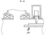
次に、図2Aおよび図2Bを用いて、本実施例の圧痕マーキングユニットの詳細について説明する。図2Aは欠陥レビュー時の試料室内および圧痕マーキングユニットの動作を示す模式図である。試料室108内では、電子線201が対物レンズ202で絞られ、ウェーハ203に照射される。ウェーハ203はステージ204上に載せられ、ステージ制御ユニット1105により任意の位置に移動される。走査電子顕微鏡画像の取得条件によっては、一次電子線を試料203の直前で減速させて試料203を撮像する場合もあり、その場合には、リターディングユニット205によりリターディング電圧が試料203に印加される。
レビュー時にはステージ204が欠陥位置に次々と移動して、対物レンズ202で絞られ電子線201を照射して欠陥のSEM画像取得を行う。このSEM画像を使用して、欠陥検出部111で欠陥の検出を行い、更に欠陥分類部で欠陥の分類を行い、元のSEM画像の他に欠陥検出結果,欠陥分類結果を、通信用コンピューター106を使い、ネットワークを通じて、YMS101にアップロードする。
図2Bに圧痕マーキング実施時の試料室内を示す。圧痕マーキング実施時には、マーキング対象欠陥抽出ユニット1104で求められたマーキング対象欠陥の位置を用いてステージ制御ユニット1105がステージ204を制御し、ウェーハ203上のマーキング目標位置を圧痕マーキングユニット109の下に移動させる。
移動が完了すると、圧痕マーキングユニット109は、真空ベローズ206を有し、垂直駆動機構207によりシャフト208の先端に取り付けられた圧子209を降下させ押し当てることにより、試料上に圧痕マーキングを形成する。これらの圧痕マーキングユニットの動作は、圧痕マーキングユニット制御ユニット1102により制御される。
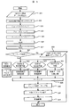
次に、図3を用いて本実施例の欠陥レビュー装置の動作について説明する。
まず、ステップ301でYMSから検査データを読み込む。ステップ302では、検査データに含まれる欠陥からADR対象欠陥を抽出するサンプリングを行う。サンプリングの目的は、欠陥数が多い場合に限られた時間で効果的なADRができるように対象欠陥を絞ることであり、クラスタ欠陥の抽出・除去、クラスタ欠陥以外からのランダム抽出等の手法が用いられる。ステップ303でウェーハアライメントを行い、ウェーハの大まかな位置合わせを行う。ステップ304でフォーカスマップを取り、フォーカスのウェーハ面内領域毎の分布を補正して、オートフォーカスが短時間で合うようにする。ステップ305ではSEMのファインアライメントが実行される。ファインアライメントは、パターン付きウェーハの場合にはホトプロセスのマスクショット単位に特異なパターンを用いて行われ、ノンパターンウェーハの場合には光学顕微鏡、特にレーザ光による暗視野顕微鏡等で欠陥を光らせて欠陥位置を正確に検出することにより行われる。ステップ306でADRにより欠陥の正確な位置を検出して、欠陥を中心にSEM画像を取得する。ステップ307ではSEM画像を元にADCで分類結果を決定する。
ステップ307のADC後、ADC部112から制御部110内のマーキング対象欠陥抽出ユニット1104に分類結果が転送され、マーキング対象欠陥抽出ユニット1104が分類された欠陥がマーキング対象かどうかを判断しマーキング対象の欠陥を抽出する(ステップ321)。マーキング対象となる欠陥が分類結果に含まれていない場合は、通信用コンピューター106を介してADR/ADC結果をYMS101にアップロードして終了する(ステップ308)。
ステップ321でマーキング対象と判断した場合、マーキング対象欠陥抽出ユニット1104は、ADC分類結果を以下の3つのカテゴリーに分類するステップを実行する。ここで、欠陥位置にマーキングを行うと、欠陥自体に影響を与え、正確な故障解析ができなくなるため、欠陥位置にマーキングを行うことはできない。したがって、マーキングの際には適当なマーキング中心を決め、欠陥毎にマーキング中心からの距離を変えてマーキングを行う。このため、欠陥の形状,サイズといったADCの分類結果の情報の他、欠陥毎にマーキングの中心位置を決定する処理が必要となる。
(1)SEM観察可能(ステップ322)
(2)SEM観察不可、かつ光学顕微鏡観察可(ステップ323)
(3)SEM観察不可、かつ光学顕微鏡観察不可(ステップ324)
ADC分類結果を以上3種のカテゴリーに分類した後は、各カテゴリー毎にマーキングの中心を決定するステップを実行する。
(1)SEM観察可能(ステップ322)
(2)SEM観察不可、かつ光学顕微鏡観察可(ステップ323)
(3)SEM観察不可、かつ光学顕微鏡観察不可(ステップ324)
ADC分類結果を以上3種のカテゴリーに分類した後は、各カテゴリー毎にマーキングの中心を決定するステップを実行する。
(1)の場合には、SEM画像の視野中心をマーキングの中心位置として決定する(ステップ325)。(2)の場合には、光学顕微鏡画像の視野中心をマーキングの中心位置として決定する(ステップ326)。マーキング中心を決定するために使用する光学顕微鏡画像としては、ステップ305で取得した光学顕微鏡画像を使用する。(3)の場合には、明視野光学式外観検査装置、暗視野光学式外観検査装置あるいは電子線式外観検査装置といった外部の検査装置から受け取った元々の検査データの欠陥座標を用いて、マーキング中心を決定する(ステップ327)。
マーキング中心が決定すれば、マーキング対象欠陥抽出ユニット1104が決定されたマーキング中心を元にマーキング座標を決定し、圧痕マーキングユニット制御ユニット1102に伝送する。圧痕マーキングユニット制御ユニット1102は、圧痕マーキングユニット109を制御して、ステップ328で決定された座標位置に実際にマーキングを行う。
次に、図4を用いて本実施例のマーキング位置の決定方法を説明する。図4は、本実施例のマーキング位置を示す模式図である。マーキング中心は欠陥501のほぼ中心に設定されており、マーキング中心からXY方向に距離D1だけ離れた位置に第1の圧痕マーキング502が打たれる。距離D1は、圧痕マーキングの座標精度や周囲への影響を考慮して決められる。第1の圧痕マーキング502は、欠陥を取り囲み正方形の頂点4点に打たれ、故障解析装置の操作者はこの中で欠陥を探せばよいことになる。更に、欠陥の近傍にはEBマーキング504より断面加工位置を示すマーキングを行う。EBマーキングとは、試料に対して一次電子線201を数分程度当ててEBコンタミを発生させて形成するマーキングである。EBマーキングは、SEMの倍率に従ったサイズで形成することが可能であるため位置精度が高く、解析装置に備えられた撮像装置で得られる画像上でも正確な加工位置を示すことができる。
ウェーハを割断する場合には、第1の圧痕マーキングの更に外側に目印があった方が割断作業がしやすい場合がある。そのような場合には、解析装置の試料ホルダーに収まるサイズから座標ずれ等の余裕を見て距離D2を決定し、マーキング中心からXY方向に距離D2だけ離れた正方形の頂点4点に第2の圧痕マーキング503を打つ。このマークはできるだけ大きめに打つことにより、目視での視認性を良くすることにより、ウェーハ割断,チップ化の作業効率が非常に良くなる。以上のように、目的に応じて複数のマーキングを使い分けることで、ウェーハ割断時、解析装置によるビーム照射位置の探索時といった各種の作業時の作業効率を高めることができる。
マーキング対象の全欠陥に対してマーキングを行った後、マーキングを終了し、試料203を欠陥レビュー装置から搬出する。
上記圧痕マーキングあるいはEBマーキングは、装置の操作者がマニュアル処理で行うことも装置に自動実行させることも可能である。自動実行させる場合には、上記の距離D1,D2およびEBマーキング位置のマーキング中心からの距離を、欠陥種あるいは欠陥サイズといった欠陥特徴量に応じてテーブル化しておき、制御部110内のメモリに格納しておく。そして、ステージ制御ユニット1105がメモリ内のテーブルを読み出し、マーキング目標位置を圧痕マーキングユニットあるいは電子光学カラムの下に移動する。
試料203の搬出後、人手により解析対象を決定する。解析対象の選定方法としては、全体の中で出現率の高いメイン欠陥、そのウェーハに特異なレア欠陥、各種欠陥から数個ずつ選択して、全体状況を大まかに見る等の方法がある。
さらにウェーハを割断,チップ化して、解析装置のホルダーに収まるサイズにする(ステップ329)。ステップ330でそのチップをFIBに入れ、FIB内で欠陥位置を探し出し、必要に応じてデポ等により表面の保護等を行った後、観察したい断面をFIB加工し、更に薄膜化して試料として取り出す。ステップ331では、TEMや高分解能SEMなどを用いて得られた薄片の断面観察を行う。
従来の方法では、故障解析の対象となる欠陥であっても欠陥探索用の目印が無い状態で試料がFIBに搬入される場合が多く、FIBで欠陥を探す部分で時間を要していた。特にパターンのないベアウェーハ等では、微小欠陥を探し出すのに大変時間を要していた。本実施例によれば、欠陥レビュー装置で重要欠陥に直接圧痕マーキングを付与できるため、解析装置側での加工位置の探索が、従来よりも非常に効率的になる。
以上、本実施例では、予め決められた戦略に従い重要な欠陥を後段の解析対象を選択することができるようになるため、早期の欠陥原因究明,歩留まり改善が可能となる。更に、SEMで観察できない欠陥も解析できるようになり、ベアウェーハの品質向上,歩留まり改善が可能となる。
〔実施例2〕
実施例1では、マーキング中心を基準としてマーキングの座標位置を決めた欠陥レビュー装置の構成例について説明したが、本実施例では、別な手法によりマーキングの座標位置を決める機能を備える欠陥レビュー装置の構成について説明する。装置の全体構成は、図1に示す場合と同様であるので、以下では、装置の構成要素および機能のうち同一な部分については説明は省略し、また適宜図1を引用する。
実施例1では、マーキング中心を基準としてマーキングの座標位置を決めた欠陥レビュー装置の構成例について説明したが、本実施例では、別な手法によりマーキングの座標位置を決める機能を備える欠陥レビュー装置の構成について説明する。装置の全体構成は、図1に示す場合と同様であるので、以下では、装置の構成要素および機能のうち同一な部分については説明は省略し、また適宜図1を引用する。
前述の通り、欠陥中心にマーキングを行うと欠陥自体に影響を与えるため、欠陥位置にマーキングを行うことは不可である。ところが、マーキング中心からのマーキング位置を画一的に決めて(例えば、距離D1,D2といったように)マーキングを行った場合、欠陥の形状や大きさによっては、欠陥位置にマーキングを行ってしまう事象が発生する場合がある。
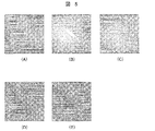
これを示すため、図5に、暗視野光学顕微鏡によるベアウェーハの特徴的な欠陥の画像例を示す。(A)は異物、(B)はPID(Polishing Induced Defect)、(C)はシャロースクラッチ(Shallow Scratch)、(D)はスリップ、(E)は積層欠陥(Stacking Fault)である。この場合、(A),(B)はSEM観察可能、(C),(D)はSEM観察不可、かつ光学顕微鏡観察可、(E)はSEM観察不可、かつ光学顕微鏡観察不可というカテゴリに分類されるケースが多いが、サイズ等の影響で一定ではない。このように、欠陥レビュー装置で検出される欠陥の形状,サイズは欠陥毎に全くまちまちである。
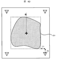
次に、図6Aおよび図6Bを用いて、不適切な圧痕マーキングが行われた欠陥の例について説明する。図6Aは、圧痕マーキングが不適切である第一の例を示す。欠陥は線状欠陥601であり、元々の設定よりもかなり長さのある欠陥である。EBマーキング604は特に問題はないが、欠陥中心602から距離D1離れた圧痕マーキング603は一部欠陥にかかってしまっている。図6Bは、圧痕マーキングが不適切な第二の例を示す。欠陥は巨大欠陥611であり、欠陥中心602から距離D1離れた圧痕マーキング603は全て欠陥にかかっている。またEBマーキング604も欠陥にかかってしまい、位置確認に使いにくくなっている。
図6Cには、図6Aに示すマーキング例の改善案を示す。マーキング対象と判断された欠陥が線状欠陥であった場合、制御部内のマーキング対象欠陥抽出ユニット1104は、欠陥を内包する最小正方形621を求める。この演算処理は、欠陥画像の端点の座標を用いて行うことができる。更にマーキング対象欠陥抽出ユニット1104は、求めた最小正方形621の頂点の座標に距離D1を足した位置を第1の圧痕マーキング位置として設定する。EBマーキングの位置は基本設定通りとする。
図6Dには、図6Bに示すマーキング例の改善案を示す。マーキング対象と判断された欠陥が巨大欠陥であった場合、図6Cと同様に、これを内包する最小正方形631を求め、最小正方形621の頂点の座標に距離D1を足した位置を第1の圧痕マーキング位置として設定する。更に、EBマーキングの位置も、最小正方形621の辺からEBマーキング用の設定距離だけ外側にずらした位置に設定する。
以上の機能を装置実装する場合には、上記の距離D1,D2,EBマーキング用距離といった距離情報に加えて、欠陥種に応じたマーキング位置算出の演算手順をテーブル化して、制御部110内のメモリに格納する。そして、マーキング対象欠陥抽出ユニット1104がメモリ内のテーブルを参照し、欠陥に応じたマーキング目標位置を設定する。設定されたマーキング目標位置の情報は、圧痕マーキングユニットおよびステージ制御ユニットにより参照され、所定の目標位置に圧痕マーキングが付与される。
図7に実施例1あるいは実施例2で使用されるGUIの構成例を示す。図7に示すGUIは、通信用コンピューター106に備えられるモニタ上に表示される。701はADC結果表示部、702はADC分類結果、703は個数表示、704はADC結果画像表示部、705はADC結果画像、706はスライドバー、707はマーキング対象画像表示部、708はマーキング対象画像、709はマーキング対象選択ボタン、710はマーキング対象解除ボタン、711はマーキング実行ボタンである。
ADC結果表示部701内に表示されるADC分類結果702,個数表示703を参考にして、ADC結果画像表示部704内に表示されるADC結果画像705をスライドバー706で動かしながら、マーキング対象を決定する。決定は画像を選んだ状態でマーキング対象選択ボタン709を押すことで決定される。あるいは、ADC結果画像705をマーキング対象画像表示部707にドラッグ・アンド・ドロップすることでも同様の結果が得られる。選択されたADC画像705はマーキング対象画像表示部707にマーキング対象画像708として追加表示される。一度追加されたマーキング対象画像708を選択し、マーキング対象解除ボタン710を押すことで対象から外すこともできる。マーキング対象画像708の選択が全て終わった後、マーキング実行ボタン711を押すことでマーキングが開始される。
以上、本実施例により、欠陥形状によりマーキングの距離を変えることが可能となるため、解析の前処理に置ける失敗が低減される。
101 YMS
102 明視野光学式外観検査装置
103 暗視野光学式外観検査装置
104 電子線式外観検査装置
105 欠陥レビュー装置
106 通信用コンピューター
107 走査電子顕微鏡カラム
108 試料室
109 圧痕マーキングユニット
110 制御部
111 ADR部
112 ADC部
113 光学顕微鏡(OM)
201 電子線
202 対物レンズ
203 試料(ウェーハ)
204 ステージ
205 リターディングユニット
206 真空ベローズ
207 垂直駆動機構
208 シャフト
209 圧子
501 欠陥
502 圧痕マーキング(小)
503 圧痕マーキング(大)
504,604 EBマーキング
601 線状欠陥
602 欠陥中心位置
603 圧痕マーキング
611 巨大欠陥
621 線状欠陥を内包する最小正方形
631 巨大欠陥を内包する最小正方形
701 ADC結果表示部
702 ADC分類結果
703 個数表示
704 ADC結果画像表示部
705 ADC結果画像
706 スライドバー
707 マーキング対象画像表示部
708 マーキング対象画像
709 マーキング対象選択ボタン
710 マーキング対象解除ボタン
711 マーキング実行ボタン
1101 電子光学カラム制御ユニット
1102 圧痕マーキングユニット制御ユニット
1103 光学顕微鏡制御ユニット
1104 マーキング対象欠陥抽出ユニット
1105 ステージ制御ユニット
102 明視野光学式外観検査装置
103 暗視野光学式外観検査装置
104 電子線式外観検査装置
105 欠陥レビュー装置
106 通信用コンピューター
107 走査電子顕微鏡カラム
108 試料室
109 圧痕マーキングユニット
110 制御部
111 ADR部
112 ADC部
113 光学顕微鏡(OM)
201 電子線
202 対物レンズ
203 試料(ウェーハ)
204 ステージ
205 リターディングユニット
206 真空ベローズ
207 垂直駆動機構
208 シャフト
209 圧子
501 欠陥
502 圧痕マーキング(小)
503 圧痕マーキング(大)
504,604 EBマーキング
601 線状欠陥
602 欠陥中心位置
603 圧痕マーキング
611 巨大欠陥
621 線状欠陥を内包する最小正方形
631 巨大欠陥を内包する最小正方形
701 ADC結果表示部
702 ADC分類結果
703 個数表示
704 ADC結果画像表示部
705 ADC結果画像
706 スライドバー
707 マーキング対象画像表示部
708 マーキング対象画像
709 マーキング対象選択ボタン
710 マーキング対象解除ボタン
711 マーキング実行ボタン
1101 電子光学カラム制御ユニット
1102 圧痕マーキングユニット制御ユニット
1103 光学顕微鏡制御ユニット
1104 マーキング対象欠陥抽出ユニット
1105 ステージ制御ユニット
Claims (13)
- 試料上における既知の欠陥位置の走査電子顕微鏡画像を取得して、前記欠陥位置の観察を行う機能を有する欠陥レビュー装置において、
前記欠陥位置に一次電子線を照射し、得られる二次電子あるいは反射電子を検出信号として出力する電子光学カラムと、
前記試料を載置し移動することにより、該試料上における前記一次電子線の照射位置を変更する試料ステージと、
前記検出信号から得られる欠陥画像を用いて、前記試料上の欠陥がマーキングの対象となる欠陥か対象とならない欠陥かに分類する欠陥分類ユニットとを備え、
前記マーキング対象となる欠陥に対し、当該欠陥の周囲に前記一次電子線による電子ビームマーキングを行う欠陥レビュー装置。 - 試料上における既知の欠陥位置の走査電子顕微鏡画像を取得して、前記欠陥位置の観察を行う機能を有する欠陥レビュー装置において、
前記欠陥位置に一次電子線を照射し、得られる二次電子あるいは反射電子を検出信号として出力する電子光学カラムと、
前記試料を載置し移動させることにより、前記電子光学カラムの撮像視野を変更する試料ステージと、
前記欠陥の周囲の複数位置に圧痕によるマーキングを付与する圧痕マーキングユニットとを備えることを特徴とする欠陥レビュー装置。 - 請求項2に記載の欠陥レビュー装置において、
前記検出信号から得られる欠陥画像を用いて、前記試料上の欠陥がマーキングの対象となる欠陥か対象とならない欠陥かに分類する欠陥分類ユニットを備えることを特徴とする欠陥レビュー装置。 - 請求項3に記載の欠陥レビュー装置において、
前記マーキング対象となる欠陥について前記圧痕を付与する位置を求めるマーキング位置演算部とを備えることを特徴とする欠陥レビュー装置。 - 請求項3に記載の欠陥レビュー装置において、
前記マーキング位置演算部は、欠陥の大きさに応じて前記圧痕を付与する位置を変えることを特徴とする欠陥レビュー装置。 - 請求項3に記載の欠陥レビュー装置において、
前記圧痕を付与する位置が前記圧痕マーキングユニットによるマーキング位置に位置するよう前記試料ステージを制御するステージ制御部を備えることを特徴とする欠陥レビュー装置。 - 請求項2に記載の欠陥レビュー装置において、
前記圧痕によるマーキングに加え、電子ビームマーキングを行うことを特徴とする欠陥レビュー装置。 - 請求項7に記載の欠陥レビュー装置において、
前記電子ビームマーキングを、前記圧痕を付与する位置よりも前記欠陥に近い位置に行うことを特徴とする欠陥レビュー装置。 - 請求項3に記載の欠陥レビュー装置において、
前記欠陥の光学顕微鏡画像を撮像する光学顕微鏡ユニットを備え、
前記欠陥分類ユニットは、前記欠陥を以下のいずれかに分類することを特徴とする欠陥レビュー装置。
1)走査電子顕微鏡画像として観察可能
2)光学顕微鏡画像としては観察可能だが走査電子顕微鏡画像とし
て観察不能
3)走査電子顕微鏡画像としても光学顕微鏡画像としても観察不能 - 請求項9に記載の欠陥レビュー装置において、
前記1)から3)の分類結果に応じて、前記圧痕を付与する位置の中心を変えることを特徴とする欠陥レビュー装置。 - 請求項10に記載の欠陥レビュー装置において、
センタリング方法はコンター抽出によることを特徴とする欠陥レビュー装置。 - 請求項1または2に記載の欠陥レビュー装置において、
前記電子ビームマーキングまたは前記圧痕によるマーキングの条件を設定する条件設定画面が表示されるモニタを備える管理用コンピュータを備え、
前記条件設定画面上に、マーキング可否の確認ボタンが表示されることを特徴とする欠陥レビュー装置。 - 請求項2に記載の欠陥レビュー装置において、
ベアウェーハに対して、異物以外をマーキング対象として抽出することを特徴とする欠陥レビュー装置。
Priority Applications (1)
| Application Number | Priority Date | Filing Date | Title |
|---|---|---|---|
| US14/116,697 US20140084159A1 (en) | 2011-05-17 | 2012-03-14 | Scanning electron microscope and method for preparing specimen |
Applications Claiming Priority (2)
| Application Number | Priority Date | Filing Date | Title |
|---|---|---|---|
| JP2011-110003 | 2011-05-17 | ||
| JP2011110003A JP2012242146A (ja) | 2011-05-17 | 2011-05-17 | 走査電子顕微鏡及び試料作成方法 |
Publications (1)
| Publication Number | Publication Date |
|---|---|
| WO2012157160A1 true WO2012157160A1 (ja) | 2012-11-22 |
Family
ID=47176516
Family Applications (1)
| Application Number | Title | Priority Date | Filing Date |
|---|---|---|---|
| PCT/JP2012/001746 Ceased WO2012157160A1 (ja) | 2011-05-17 | 2012-03-14 | 欠陥レビュー装置 |
Country Status (3)
| Country | Link |
|---|---|
| US (1) | US20140084159A1 (ja) |
| JP (1) | JP2012242146A (ja) |
| WO (1) | WO2012157160A1 (ja) |
Cited By (2)
| Publication number | Priority date | Publication date | Assignee | Title |
|---|---|---|---|---|
| CN103871918A (zh) * | 2012-12-10 | 2014-06-18 | 中芯国际集成电路制造(上海)有限公司 | 晶圆中缺陷定位的方法 |
| CN113776916A (zh) * | 2021-09-10 | 2021-12-10 | 广州机械科学研究院有限公司 | 滤膜及滤膜应用方法 |
Families Citing this family (13)
| Publication number | Priority date | Publication date | Assignee | Title |
|---|---|---|---|---|
| DE112013007337T5 (de) * | 2013-08-14 | 2016-04-28 | Hitachi, Ltd. | Halbleiter-Prüfverfahren, Halbleiter-Prüfvorrichtung und Verfahren zum Herstellen eines Halbleiterelements |
| JP6212455B2 (ja) * | 2014-03-12 | 2017-10-11 | 東芝メモリ株式会社 | マーキング装置およびマーキング方法 |
| US9696268B2 (en) * | 2014-10-27 | 2017-07-04 | Kla-Tencor Corporation | Automated decision-based energy-dispersive x-ray methodology and apparatus |
| US20160334315A1 (en) * | 2015-05-12 | 2016-11-17 | Nanovea, Inc. | Method for automated parameter and selection testing based on known characteristics of the sample being tested |
| KR101772024B1 (ko) * | 2015-10-15 | 2017-08-28 | 주식회사 엘지실트론 | 웨이퍼의 검사 방법 |
| US11002687B2 (en) | 2016-03-16 | 2021-05-11 | Hitachi High-Tech Corporation | Defect inspection method and defect inspection device |
| CN106290376B (zh) * | 2016-07-21 | 2019-04-12 | 京东方科技集团股份有限公司 | 微观缺陷检测装置及其控制方法、显微镜 |
| US10552708B2 (en) | 2018-03-07 | 2020-02-04 | Xerox Corporation | Method and system for extracting impression marks using a mobile application |
| JP7221596B2 (ja) * | 2018-03-28 | 2023-02-14 | Jx金属株式会社 | 粒状試料の分析方法及び分析装置 |
| KR20230147143A (ko) * | 2021-03-26 | 2023-10-20 | 주식회사 히타치하이테크 | 주사형 프로브 현미경, 시료 관찰 가공 시스템 및 전기 특성 평가 장치 |
| CN115577135B (zh) * | 2022-09-01 | 2026-03-24 | 中科慧远视觉技术(北京)有限公司 | 缺陷筛选方法、产品分类方法、装置和计算机设备 |
| US12536613B2 (en) | 2022-12-06 | 2026-01-27 | Samsung Electronics Co., Ltd. | Method and system with image super-resolution |
| CN116013800B (zh) * | 2022-12-30 | 2024-02-27 | 胜科纳米(苏州)股份有限公司 | 一种缺陷定位方法、装置、电子设备及存储介质 |
Citations (6)
| Publication number | Priority date | Publication date | Assignee | Title |
|---|---|---|---|---|
| JPH11354598A (ja) * | 1998-06-11 | 1999-12-24 | Hitachi Ltd | ウェハ検査装置 |
| JP2004257845A (ja) * | 2003-02-26 | 2004-09-16 | Renesas Technology Corp | 欠陥の分類方法 |
| JP2006506816A (ja) * | 2002-11-12 | 2006-02-23 | エフ・イ−・アイ・カンパニー | 欠陥分析器 |
| JP2008177282A (ja) * | 2007-01-17 | 2008-07-31 | Renesas Technology Corp | 半導体装置の製造方法 |
| JP2009110978A (ja) * | 2009-02-18 | 2009-05-21 | Hitachi Ltd | イオンビーム装置 |
| JP2009139379A (ja) * | 2007-12-06 | 2009-06-25 | Fei Co | デコレーションを用いたスライス・アンド・ビュー |
Family Cites Families (1)
| Publication number | Priority date | Publication date | Assignee | Title |
|---|---|---|---|---|
| JP5384786B2 (ja) * | 2006-11-14 | 2014-01-08 | 株式会社日立ハイテクノロジーズ | 荷電ビーム装置、及びその鏡体 |
-
2011
- 2011-05-17 JP JP2011110003A patent/JP2012242146A/ja active Pending
-
2012
- 2012-03-14 US US14/116,697 patent/US20140084159A1/en not_active Abandoned
- 2012-03-14 WO PCT/JP2012/001746 patent/WO2012157160A1/ja not_active Ceased
Patent Citations (6)
| Publication number | Priority date | Publication date | Assignee | Title |
|---|---|---|---|---|
| JPH11354598A (ja) * | 1998-06-11 | 1999-12-24 | Hitachi Ltd | ウェハ検査装置 |
| JP2006506816A (ja) * | 2002-11-12 | 2006-02-23 | エフ・イ−・アイ・カンパニー | 欠陥分析器 |
| JP2004257845A (ja) * | 2003-02-26 | 2004-09-16 | Renesas Technology Corp | 欠陥の分類方法 |
| JP2008177282A (ja) * | 2007-01-17 | 2008-07-31 | Renesas Technology Corp | 半導体装置の製造方法 |
| JP2009139379A (ja) * | 2007-12-06 | 2009-06-25 | Fei Co | デコレーションを用いたスライス・アンド・ビュー |
| JP2009110978A (ja) * | 2009-02-18 | 2009-05-21 | Hitachi Ltd | イオンビーム装置 |
Cited By (3)
| Publication number | Priority date | Publication date | Assignee | Title |
|---|---|---|---|---|
| CN103871918A (zh) * | 2012-12-10 | 2014-06-18 | 中芯国际集成电路制造(上海)有限公司 | 晶圆中缺陷定位的方法 |
| CN113776916A (zh) * | 2021-09-10 | 2021-12-10 | 广州机械科学研究院有限公司 | 滤膜及滤膜应用方法 |
| CN113776916B (zh) * | 2021-09-10 | 2024-04-26 | 广州机械科学研究院有限公司 | 滤膜及滤膜应用方法 |
Also Published As
| Publication number | Publication date |
|---|---|
| JP2012242146A (ja) | 2012-12-10 |
| US20140084159A1 (en) | 2014-03-27 |
Similar Documents
| Publication | Publication Date | Title |
|---|---|---|
| JP2012242146A (ja) | 走査電子顕微鏡及び試料作成方法 | |
| JP4307470B2 (ja) | 荷電粒子線装置、試料加工方法及び半導体検査装置 | |
| US7755776B2 (en) | Inspection system and inspection method | |
| US7612337B2 (en) | Focused ion beam system and a method of sample preparation and observation | |
| JP5202071B2 (ja) | 荷電粒子顕微鏡装置及びそれを用いた画像処理方法 | |
| JP6618380B2 (ja) | 自動化されたs/tem取得および測定のための既知の形状の薄片を使用したパターン・マッチング | |
| JP2001159616A (ja) | パターン検査方法及びパターン検査装置 | |
| JPH10213422A (ja) | パタ−ン検査装置 | |
| US20120262723A1 (en) | Surface inspection tool and surface inspection method | |
| JP7410164B2 (ja) | 検査システム、及び非一時的コンピュータ可読媒体 | |
| US20130134308A1 (en) | Sample observation apparatus and method of marking | |
| WO2010079657A1 (ja) | Semを用いた欠陥観察方法及びその装置 | |
| CN106796188A (zh) | 基于自动化决策的能量分散式x射线方法及设备 | |
| TWI769205B (zh) | 缺陷分析 | |
| JP4745380B2 (ja) | レビューsem | |
| JP2013246001A (ja) | 荷電粒子線装置及び試料作成方法 | |
| JP4604734B2 (ja) | ウェーハの評価方法 | |
| EP3070731A1 (en) | Pattern matching using a lamella of known shape for automated s/tem acquisition and metrology | |
| JPH11340291A (ja) | 半導体デバイス検査分析方法及びそのシステム並びに半導体デバイスの製造方法 | |
| JP4842782B2 (ja) | 欠陥レビュー方法および装置 | |
| JP2006227026A (ja) | パターン検査方法及びパターン検査装置 | |
| TW202548825A (zh) | 未圖案化表面樣品的缺陷檢測 | |
| JP2014130745A (ja) | 荷電粒子線装置 | |
| JP2017027651A (ja) | 荷電粒子線装置およびプログラム記憶媒体 | |
| JP2018525811A (ja) | 設計を利用する先行層欠陥箇所の点検 |
Legal Events
| Date | Code | Title | Description |
|---|---|---|---|
| 121 | Ep: the epo has been informed by wipo that ep was designated in this application |
Ref document number: 12784912 Country of ref document: EP Kind code of ref document: A1 |
|
| WWE | Wipo information: entry into national phase |
Ref document number: 14116697 Country of ref document: US |
|
| NENP | Non-entry into the national phase |
Ref country code: DE |
|
| 122 | Ep: pct application non-entry in european phase |
Ref document number: 12784912 Country of ref document: EP Kind code of ref document: A1 |