WO2012153588A1 - コネクタ - Google Patents
コネクタ Download PDFInfo
- Publication number
- WO2012153588A1 WO2012153588A1 PCT/JP2012/059664 JP2012059664W WO2012153588A1 WO 2012153588 A1 WO2012153588 A1 WO 2012153588A1 JP 2012059664 W JP2012059664 W JP 2012059664W WO 2012153588 A1 WO2012153588 A1 WO 2012153588A1
- Authority
- WO
- WIPO (PCT)
- Prior art keywords
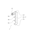
- connector
- terminal
- devices
- terminals
- tolerance
- Prior art date
- Legal status (The legal status is an assumption and is not a legal conclusion. Google has not performed a legal analysis and makes no representation as to the accuracy of the status listed.)
- Ceased
Links
Images





Classifications
-
- H—ELECTRICITY
- H01—ELECTRIC ELEMENTS
- H01R—ELECTRICALLY-CONDUCTIVE CONNECTIONS; STRUCTURAL ASSOCIATIONS OF A PLURALITY OF MUTUALLY-INSULATED ELECTRICAL CONNECTING ELEMENTS; COUPLING DEVICES; CURRENT COLLECTORS
- H01R13/00—Details of coupling devices of the kinds covered by groups H01R12/70 or H01R24/00 - H01R33/00
- H01R13/46—Bases; Cases
- H01R13/516—Means for holding or embracing insulating body, e.g. casing, hoods
- H01R13/518—Means for holding or embracing insulating body, e.g. casing, hoods for holding or embracing several coupling parts, e.g. frames
-
- H—ELECTRICITY
- H01—ELECTRIC ELEMENTS
- H01R—ELECTRICALLY-CONDUCTIVE CONNECTIONS; STRUCTURAL ASSOCIATIONS OF A PLURALITY OF MUTUALLY-INSULATED ELECTRICAL CONNECTING ELEMENTS; COUPLING DEVICES; CURRENT COLLECTORS
- H01R13/00—Details of coupling devices of the kinds covered by groups H01R12/70 or H01R24/00 - H01R33/00
- H01R13/46—Bases; Cases
- H01R13/514—Bases; Cases composed as a modular blocks or assembly, i.e. composed of co-operating parts provided with contact members or holding contact members between them
Definitions
- the present invention relates to a connector that can collectively connect terminals of a plurality of devices.
- a single device is configured by assembling a stack 103 of devices in which a plurality of devices 102 such as a substrate provided with terminals 101 are stacked.
- a connector fitting portion 104 is formed at an end of the laminated body 103 of the device.
- the connector 201 can be fitted to the connector fitting portion 104 of the stacked devices 103, and the terminals 101 of the plurality of devices 102 can be collectively connected by the connector 201.
- a tolerance is generated due to the stacking of the devices 102, so that the terminal position is deviated from the design value.
- the connector 201 is directly fitted to the connector fitting portion 104 and connected to a device, it is necessary to fit the connector 201 in consideration of tolerance due to lamination. That is, since the position of the terminal 101 of the connector fitting portion 104 is misaligned due to tolerance, the misalignment must be absorbed by some means.
- Patent Document 1 Conventionally, for example, a method described in Patent Document 1 is known as a means for absorbing a positional shift between the connector 201 and the terminal 101.
- the connector housing is structurally separated from the main cover, the main cover is provided with an opening larger than the outer periphery of the connector housing, and the connector housing is formed by a flexible and severable holding portion. Hold it movably in the opening, form a connector housing movement space that is higher than the tab terminal height between the connector housing and the wiring board, and pass the tab terminal through the insertion hole of the connector housing after cutting the holding part.
- the connector part is formed by
- Patent Document 1 does not connect a connector to a connector fitting portion in which a plurality of devices are stacked.
- Patent Document 1 is different in basic form from the case of connecting terminals of a laminated device as shown in FIG.
- An object of the present invention is to solve the above-described problems of the prior art.
- a connector is fitted to a connector fitting portion in which a plurality of devices are stacked to connect the terminal and the connector of the device, the device side
- the connector of the present invention is A connector for connecting terminals of a plurality of devices collectively by fitting to a laminate in which a plurality of devices having terminals at the end are stacked, Independent connector parts for connecting to the terminals of each of the above devices are configured to be coupled in the stacking direction of the devices,
- the connector component has a terminal main body portion for connecting to the terminal of the device, and a connecting portion for connecting the connector components to each other in the stacking direction of the device,
- the connecting portion is formed so that the connector component can individually follow the terminal of the device and absorb the tolerance with respect to the tolerance due to the stacking of the devices.
- one connector part corresponds to one device.
- the connecting portion includes a convex portion and a concave portion provided on an upper surface and a lower surface of the connector component.
- the plurality of connector parts are all formed in the same shape.
- a fixing part for preventing the connector from being detached when the connector is fitted to the device is formed in the connector part.
- the fixing portion is formed on a side surface of the connector part.
- the connector has a regulating member that regulates the direction of the electric wire on the side opposite to the terminal joining direction of the connector.
- the connector part has an attachment portion for attaching the restriction member.
- the restricting member is fixed to one connector part of the plurality of connector parts.
- the connector of the present invention is configured by connecting independent connector parts for connecting to terminals of each device in the stacking direction of the devices, and the connector parts are connected to terminal terminals of the devices;
- the connector part has a connecting part for connecting the connector parts to each other in the stacking direction of the equipment, and the connecting part follows the terminal of the equipment individually with respect to tolerance due to the stacking of the equipment. Since the tolerance is formed so as to be absorbed, the tolerance due to the lamination of the laminated body of the devices can be absorbed by the connector side connecting portion. For this reason, even if the position of the terminal of the laminated body of the device fluctuates due to the tolerance, the connecting portion absorbs the tolerance, and the connector can be easily fitted to the connector fitting portion of the device. Connection is possible.
- FIG. 4 is a cross-sectional view taken along line AA in FIG. 3.
- AA in FIG. 3.
- a disassembled perspective view of the connector of FIG. It is a rear view of the connector component of FIG.
- a bottom view of the connector component of FIG. It is the perspective view which looked at the control member of FIG. 1 from diagonally downward.
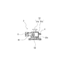
- sectional drawing which shows the state which fitted the connector of FIG. 1 to the connector fitting part. It is explanatory drawing which shows the outline of the laminated body of the conventional connector and apparatus.
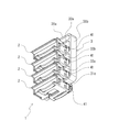
- FIG. 1 is a perspective view showing a connector fitting portion of a connector and an apparatus according to an embodiment of the present invention.
- the connector 1 of the present invention is fitted to a laminated body 12 of a device in which a plurality of devices 11 such as a substrate having terminals 10 at the end are stacked, and a plurality of terminals 10 of the plurality of devices 11. It is a connector for connecting all together.
- the connector 1 is formed as a connector for collectively connecting four terminals 10 of a laminate 12 in which four devices 11 are laminated.
- the periphery of the terminal 10 is formed as a recess.
- a collection of concave portions of the terminal 10 is formed as a connector fitting portion 13 into which the connector 1 can be fitted.
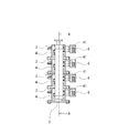
- FIG. 2 is a perspective view of the connector of FIG. 1 as viewed obliquely from below.
- FIG. 3 is a front view of the connector of FIG. 4 is a cross-sectional view taken along the line AA in FIG.
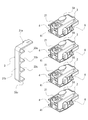
- FIG. 5 is an exploded perspective view of the connector of FIG.
- the connector 1 has connector parts 2, 2, 2, 2 composed of four independent members connected in the same direction as the stacking direction of the devices 11 (Z-axis direction in FIG. 1). And integrated.
- the number of connectors 1 corresponding to the number of devices 11 is provided so that each connector component 2 is fitted to each terminal 10 of the device 11.
- a regulating member 3 for regulating the direction of the electric wire is mounted on the connector 1 on the side opposite to the terminal fitting direction (front side in FIG. 1).
- the restricting member 3 is fixed to the uppermost connector part 2.
- the connector component 2 includes a terminal body 4 for connecting to the terminal 10 of the device 11 and a connecting portion 5 for connecting the plurality of connector components 2 in the stacking direction.
- the connecting portion 5 includes a convex portion 51 provided on the upper surface of the terminal body 4 and a concave portion 52 provided on the lower surface.
- the connector part 2 is provided with a fixing portion 6 on one side surface for preventing the connector 1 from coming off the device 11 when the connector 1 is fitted to the connector fitting portion 13 of the device 11. (See FIG. 5).
- FIG. 6 is a rear view of the connector part of FIG. 1, and FIG. 7 is a bottom view of the connector part of FIG.
- the connector body 4 is provided with a cavity inside, and a female terminal 41 is mounted in the cavity.
- the terminal 41 is connected to the terminal 10 on the device side (rear in FIG. 1), and connected to a terminal (not shown) connected to the wire harness wire on the opposite side (front in FIG. 1). .
- the connecting portion 5 serves to connect the connector parts 2 to each other in the stacking direction of the devices 11 and has a function as a tolerance absorbing portion of the connector 1.
- the convex portion 51 of the connecting portion 5 is formed with an insertion portion 51 a that protrudes from the surface of the terminal body 4 and is inserted into the concave portion 52, and is narrower than the insertion portion 51 a, and the insertion portion 51 a and the terminal It consists of a support portion 51b for connecting the main body 4.
- the recess 52 of the connecting portion 5 has an opening 52 a that opens on the device 1 side and a notch 52 b that is cut off on the lower surface.
- the opening 52 a of the recess 52 is formed to have a width that allows the insertion portion 51 a of the projection 51 to be inserted.
- the cutout portion 52b of the concave portion 52 is formed wider than the support portion 51b of the convex portion 51 and narrower than the insertion portion 51a.
- a hemispherical protrusion 52c is provided on the opening 52a side of the recess 52.
- the connecting portion 5 is formed so that the convex portion 51 of another connector component is slidably fitted into the concave portion 52. That is, when the convex portion 51 is inserted and slid through the insertion portion 51 a from the opening 52 a side (see FIG. 7) of the concave portion 52, the support portion 51 b is guided by the notch portion 52 b and fitted into the concave portion 52. With the insertion portion 51a slidably fitted in the recess 52, the insertion portion 51a moves in the recess 52 in the vertical direction (Z direction in FIG. 1), left and right direction (X direction in FIG. 1), and front and rear direction (Y in FIG. 1). The insertion part 51a and the recessed part 52 are formed so that it can move freely in the direction).
- the height of the recess 52 is formed larger than the thickness of the insertion portion 51a. Further, the length of the recess 52 in the front-rear direction is formed larger than the length of the insertion part 51 in the front-rear direction. Further, the widths of the recess 52 and the notch 52b in the left-right direction are formed larger than the widths of the insertion part 51a and the support part 51b, respectively.
- the insertion portion 51 a of the convex portion 51 is slid to the opening portion side in contact with the terminal body 4 on the upper surface of the opening portion 52, the insertion portion 51 a is provided on the opening portion 52 side.
- the projection 52c is in contact with the projection 52c so that it does not come out of the opening 52a.
- the convex part 51 freely moves within a predetermined range in the vertical and horizontal directions and the front and rear directions in the concave part 52.
- the connecting part 5 is formed as a tolerance absorbing part.
- the connector parts 2 and 2 can move within a predetermined range in the X direction, the Y direction, and the Z direction independently of each other.
- the tolerance is absorbed by the connecting portion 5 so that each connector component 2 follows the position of each terminal 10 independently.
- a fixing portion 6 is provided on the right side surface of the connector part 2 to prevent the connector part 2 from coming out of the device 11 when the connector 1 is fitted to the device 11. Yes.
- the fixing portion 6 includes a spring portion 61 protruding from the end portion of the terminal body 4 to the side surface, a locking portion 62 for locking to the connector fitting portion of the device 11, and a spring portion. It is comprised from the knob
- pick part 63 currently formed in the front side edge part of 61.
- the spring portion 61 When inserting and fitting the connector part into the connector fitting portion, the spring portion 61 is bent and the locking portion 62 is locked to the engaging portion (not shown) of the connector fitting portion 13. In a state where the locking portion 62 is locked to the engaging portion, the connector part 2 is prevented from being detached from the connector fitting portion 13 due to the elasticity of the spring portion 61.
- the knob part 63 When detaching the connector part 2 from the connector fitting part 13, the knob part 63 is picked with a finger or the like, and the spring part 61 is pressed toward the terminal body 4 to release the locking of the locking part 62 to the device 11. Be able to. When the knob portion 63 is pressed against the terminal body side 4, the spring portion 61 is bent and the locking portion 62 can be released from the engaged state.
- each terminal 10 of the connector fitting portion 13 is misaligned due to tolerance in the laminating direction (Z direction), or misaligned due to tolerance in the horizontal horizontal direction (X direction). In other words, positional deviation in the horizontal front-rear direction (Y direction) occurs.
- Z direction laminating direction
- X direction horizontal horizontal direction
- Y direction positional deviation in the horizontal front-rear direction
- FIG. 8 is a perspective view of the regulating member of FIG. 1 as viewed obliquely from below.
- the regulating member 3 includes a main body 31 that is a U-shaped flat plate in a side view, a locking portion 32 provided at one end, and three partition plates in the middle. 33a, 33b, 33c.
- the main body 31 includes an upper horizontal plate 31a, a lower horizontal plate 31c, and a vertical plate 31b therebetween.
- the locking portion 32 of the regulating member 3 is provided on the upper horizontal plate 31a of the main body 31 in a wedge shape that protrudes downward.
- the locking portion 32 is for attaching and holding the regulating member 3 to the connector part 2.
- the restricting member 3 is fixedly held by being inserted into the attachment portion 21 of the uppermost connector part 2.
- the regulating member 3 is provided so as to be positioned in front of the female terminal 41 as shown in FIGS.
- the partition plate 32 defines a space in front of the entire terminal 41 of each connector component.
- the regulating member 3 regulates the direction of the wire harness connected to the terminal 41. That is, the electric wire connected to the terminal 41 is bent in the left-right direction by the vertical plate 31 b of the regulating member 3. Further, the electric wire connected to the terminal 41 is divided into upper and lower portions by the partition plates 33a to 33c of the regulating member 3, the upper horizontal plate 31a, the lower horizontal plate 31c, and the like. Thus, since the regulating member 3 can regulate the wiring direction of the plurality of electric wires connected to the connector 1, it is possible to satisfactorily prevent problems such as crosstalk.
- FIG. 9 is a cross-sectional view showing a state where the connector of FIG. 1 is fitted to the connector fitting portion.
- the connector 1 can be fitted into a connector fitting portion 13 (see FIG. 1) of a laminate 12 in which four devices 11 are laminated.
- the terminal 10 of the device is inserted and electrically connected to the female terminal 41 of each connector component 2.
- the connecting portion 5 Since there is play in the connection between the convex portion 51 and the concave portion 52, it can be flexibly handled.
- the connector 1 can absorb the tolerance due to the stacking of the plurality of devices 11 with the connecting portion 5 serving as the tolerance absorbing portion.
- the connector 1 of the present invention is not limited to the embodiment described above and can be modified.
- the four connector parts 2 are connected to each other.
- the number of the connector parts 2 may be at least two, and is not limited to four.
- the number of connector parts 2 is preferably formed according to the number of mating terminals.
- connection part 5 although comprised as the connection part 5 from the recessed part 52 and the convex part 51 which slide-fits to this recessed part, the connection part 5 moves flexibly so that the connector components 2 may absorb tolerance.
- the present invention is not particularly limited to the above form.
Landscapes
- Details Of Connecting Devices For Male And Female Coupling (AREA)
- Connector Housings Or Holding Contact Members (AREA)
Abstract
複数の機器を積層したコネクタ嵌合部にコネクタを嵌合して機器の端子とコネクタを接続する場合、機器側の積層公差を吸収して、機器のコネクタ嵌合部に容易に嵌合が可能であり、確実な端子の接続を行うことが可能であるコネクタを提供する。 各機器の端子(10)に接続するための独立したコネクタ部品(2)が、前記機器(11)の積層方向に連結されて構成され、前記コネクタ部品(2が、前記機器(11)の端子(10)と接続するための端子本体部(4)と、前記コネクタ部品(2)同士を前記機器(11)の積層方向に連結するための連結部(5)を有し、前記連結部(5)は、前記機器(11)の積層による公差に対し、前記コネクタ部品(2)が前記機器(11)の端子(10)に個別に追従して、前記公差を吸収可能に形成した。
Description
本発明は、複数の機器の端子を一括して接続することが可能なコネクタに関するものである。
例えば、図10に示すように、端子101が設けられた基板等の機器102を複数積層した機器の積層体103を組み立てて、一つの装置を構成する場合がある。機器の積層体103には、端部にコネクタ嵌合部104が形成される。
図10に示すように、積層した機器103のコネクタ嵌合部104に、コネクタ201を嵌合して、複数の機器102の端子101をコネクタ201で一括して接続することができる。
複数の機器の積層体103のコネクタ嵌合部104は、機器102の積層による公差が発生するので、設計値に対して端子の位置がずれることになる。コネクタ嵌合部104に、直接コネクタ201を嵌合して機器と接続する場合、積層による公差を考慮してコネクタ201の嵌合を行う必要がある。すなわち、コネクタ嵌合部104の端子101の位置は公差による位置ずれがあるので、何らかの手段でずれを吸収しなければならない。
従来、コネクタ201と端子101の位置ずれを吸収する手段として、例えば特許文献1に記載の方法が公知である。
特許文献1に記載の方法は、コネクタハウジングをメインカバーと構造上別体にし、メインカバーにコネクタハウジングの外周より大きな開口部を設け、可撓性を有する切断可能な保持部により、コネクタハウジングを開口部に移動可能に保持し,コネクタハウジングと配線板の間に、タブ端子の高さ以上のコネクタハウジングの移動空間を形成し、保持部の切断後、コネクタハウジングの挿通孔にタブ端子を通過させることによってコネクタ部を形成したものである。
しかし上記特許文献1に記載されているコネクタは、複数の機器を積層したコネクタ嵌合部に、コネクタを接続するものではない。特許文献1は、図10に示すような積層機器の端子を接続する場合とは、基本的な形態が相違する。
従来、図10に示すような複数の機器が積層された場合の公差の吸収は、積層後の機器側で端子位置のずれを直し、公差を矯正するようにしていた。しかし、機器側で公差を矯正することは、矯正作業に非常に手間がかかり、コストが上昇してしまう。
また従来、コネクタ側では公差を吸収することができなかった為、機器側で公差の矯正が不十分な場合には、コネクタを機器に嵌合して端子との接続を行うことが不可能になってしまうという問題があった。
本発明の課題は、上記従来技術の問題点を解決しようとするものであり、複数の機器を積層したコネクタ嵌合部にコネクタを嵌合して機器の端子とコネクタを接続する場合、機器側の積層公差を吸収して、機器のコネクタ嵌合部に容易に嵌合が可能であり、確実な端子の接続を行うことができるコネクタを提供することにある。
上記課題を解決するために本発明のコネクタは、
端部に端子を有する機器が複数積層された積層体に嵌合して、複数の機器の端子を一括して接続するためのコネクタであって、
上記各機器の端子に接続するための独立したコネクタ部品が、前記機器の積層方向に連結されて構成され、
前記コネクタ部品が、前記機器の端子と接続するための端子本体部と、前記コネクタ部品同士を前記機器の積層方向に連結するための連結部を有し、
前記連結部は、前記機器の積層による公差に対し、前記コネクタ部品が前記機器の端子に個別に追従して、前記公差を吸収可能に形成されていることを、
要旨とするものである。
端部に端子を有する機器が複数積層された積層体に嵌合して、複数の機器の端子を一括して接続するためのコネクタであって、
上記各機器の端子に接続するための独立したコネクタ部品が、前記機器の積層方向に連結されて構成され、
前記コネクタ部品が、前記機器の端子と接続するための端子本体部と、前記コネクタ部品同士を前記機器の積層方向に連結するための連結部を有し、
前記連結部は、前記機器の積層による公差に対し、前記コネクタ部品が前記機器の端子に個別に追従して、前記公差を吸収可能に形成されていることを、
要旨とするものである。
上記コネクタにおいて、一つの機器に対し一つのコネクタ部品が対応していることが好ましい。
上記コネクタにおいて、前記連結部が、前記コネクタ部品の上面と下面に設けた凸部と凹部からなることが好ましい。
上記コネクタにおいて、前記複数のコネクタ部品が全て同一形状に形成されていることが好ましい。
上記コネクタにおいて、前記コネクタを前記機器に嵌合した際に、機器から抜けるのを防止するための固定部が、コネクタ部品に形成されていることが好ましい。
上記コネクタにおいて、前記固定部が、前記コネクタ部品の側面に形成されていることが好ましい。
上記コネクタにおいて、前記コネクタの端子接合方向と反対側に電線の方向を規制する規制部材を有することが好ましい。
上記コネクタにおいて、前記コネクタ部品が、前記規制部材を取り付けるための取付部を有することが好ましい。
上記コネクタにおいて、前記規制部材は、前記複数のコネクタ部品の一つのコネクタ部品に固定されていることが好ましい。
本発明コネクタは、各機器の端子に接続するための独立したコネクタ部品が、前記機器の積層方向に連結されて構成され、前記コネクタ部品が、前記機器の端子と接続するための端子本体部と、前記コネクタ部品同士を前記機器の積層方向に連結するための連結部を有し、前記連結部は、前記機器の積層による公差に対し、前記コネクタ部品が前記機器の端子に個別に追従して、前記公差を吸収可能に形成されていることにより、機器の積層体の積層による公差をコネクタ側の連結部により吸収する事ができる。そのため、機器の積層体の端子の位置が公差により変動していても、連結部が公差を吸収して、機器のコネクタ嵌合部に容易にコネクタを嵌合することができ、確実な端子の接続が可能である。
以下、図面を用いて本発明の実施例を詳細に説明する。図1は本発明の一実施例のコネクタと機器のコネクタ嵌合部を示す斜視図である。図1に示すように本発明のコネクタ1は、端部に端子10を有する基板などの機器11が複数積層された機器の積層体12に嵌合して、複数の機器11の複数の端子10を一括して接続するためのコネクタである。
図1の実施例のコネクタ1は、4つの機器11が積層された積層体12の4つの端子10を一括して接続するためのコネクタとして形成されている。コネクタが接続される相手側の機器11は、端子10の周囲が、凹部として形成されている。積層体12において、端子10の凹部の集合体が、コネクタ1が嵌合可能なコネクタ嵌合部13として形成されている。
図2は、図1のコネクタを斜め下方から見た斜視図である。図3は、図1のコネクタの正面図である。図4は図3のA-A断面図である。図5は図1のコネクタの分解斜視図である。図2~図5に示すように、コネクタ1は、4つの独立した部材からなるコネクタ部品2、2、2、2が、機器11の積層方向(図1のZ軸方向)と同じ方向に連結されて一体化して構成されている。コネクタ1は、機器11の各端子10に、各コネクタ部品2がそれぞれ嵌合するように機器11の数に対応する数だけ設けられている。更にコネクタ1の、端子嵌合方向とは反対側(図1中では正面側)に、電線の方向を規制するための規制部材3が装着されている。規制部材3は、最上部のコネクタ部品2に固定されている。
図4及び図5に示すように、4つのコネクタ部品2は、全て同一形状に形成されている。コネクタ部品2は、機器11の端子10と接続するための端子本体4と、複数のコネクタ部品2を積層方向に連結するための連結部5を有する。連結部5は、端子本体4の上面に設けられた凸部51と下面に設けられた凹部52とからなる。更に、コネクタ部品2は、一方の側面に、コネクタ1を機器11のコネクタ嵌合部13に嵌合した際に、コネクタ1が機器11から抜けるのを防止するための固定部6が設けられている(図5参照)。
図6は、図1のコネクタ部品の背面図であり、図7は図1のコネクタ部品の底面図である。図6に示すようにコネクタ本体4は、内部にキャビティが設けられ該キャビティにメス型の端子41が装着されている。端子41は、機器側(図1では後方)が端子10と接続し、機器側と反対側(図1では前方)が、ワイヤーハーネスの電線に接続された端子(図示せず)が接続される。
連結部5は、コネクタ部品2同士を機器11の積層方向に連結するためのものであると共に、コネクタ1の公差吸収部としての機能を持っている。連結部5の凸部51は、図6に示すように、端子本体4表面から突出し凹部52に挿通される挿通部51aと、該挿通部51aより狭幅に形成され、該挿通部51aと端子本体4を接続する支持部51bからなる。
連結部5の凹部52は、図6及び図7に示すように、機器1側が開口した開口部52aと、下面が切り欠かれた切り欠き部52bを有する。凹部52の開口部52aは、凸部51の挿通部51aが挿通可能な幅に形成されている。凹部52の切り欠き部52bは、凸部51の支持部51bよりも幅広で且つ挿通部51aより狭幅に形成されている。また、凹部52の開口部52a側には、半球状の突起52cが設けられている。
図4に示すように、連結部5は、凹部52に対し、他のコネクタ部品の凸部51がスライド嵌合するように形成されている。すなわち凸部51は、凹部52の開口部52a側(図7参照)から挿通部51aを挿通しスライドさせると、支持部51bが切り欠き部52bにガイドされて凹部52内に嵌合する。挿通部51aが凹部52にスライド嵌合した状態で、挿通部51aが凹部52内を、上下方向(図1中Z方向)、左右方向(図1中X方向)、前後方向(図1中Y方向)に自由に動けるように、挿通部51aと凹部52は形成されている。
すなわち凹部52の高さが、挿通部51aの厚みよりも大きく形成されている。また凹部52の前後方向の長さが、挿通部51の前後方向の長さよりも大きく形成されている。また凹部52と切り欠き部52bの左右方向の幅が、それぞれ挿通部51aと支持部51bの幅よりも大きく形成されている。
また図4に示すように、凸部51の挿通部51aが開口部52の上面の端子本体4と接した状態で開口部側にスライドさせても、挿通部51aは開口部52側に設けられている突起52cに当接して、開口部52aから外部に出ないようになっている。
コネクタ2、2が連結した状態において、連結部5では、凸部51が凹部52内を上下、左右、前後の各方向に、所定の範囲内で自由に動く。連結部5は、公差吸収部として形成されている。コネクタ部品2、2は互いに独立してX方向、Y方向、Z方向に、所定の範囲で動くことが可能である。コネクタ1は、機器の積層体12にコネクタ1を嵌合する際に、連結部5により公差を吸収して、各コネクタ部品2が独立して各端子10の位置に追従する。
図5などに示すように、コネクタ部品2の右側面には、コネクタ1を機器11に嵌合した際に、機器11からコネクタ部品2が抜けるのを防止するための固定部6が設けられている。固定部6は、図7に示すように、端子本体4の端部から側面側に突出するバネ部61と、機器11のコネクタ嵌合部に係止するための係止部62と、バネ部61の前方側端部に形成されている摘み部63とから構成されている。コネクタ部品をコネクタ嵌合部に挿入して勘合する際、バネ部61が撓んで、係止部62がコネクタ嵌合部13の係合部(図示せず)に係止される。係止部62が係合部に係止した状態では、コネクタ部品2はバネ部61の弾性により、コネクタ嵌合部13から外れないようになっている。
コネクタ嵌合部13からコネクタ部品2を取り外す場合は、摘み部63を指などで摘み、バネ部61を端子本体4側に押圧することで、係止部62の機器11に対する係止を解除することができるようになっている。摘み部63を端子本体側4に押付けると、バネ部61が撓んで係止部62を係合状態から外すことができる。
複数の機器11が積層された積層体12では、コネクタ嵌合部13の各端子10は、積層方向(Z方向)の公差による位置ずれや、水平左右方向(X方向)の公差による位置ずれや、水平前後方向(Y方向)の位置ずれ等が発生する。コネクタ1をコネクタ嵌合部13に嵌合する際、機器11の積層による公差を、複数の独立したコネクタ部品2は連結部によって公差を吸収するように連結されているので、コネクタ部品2を各機器11の端子10に個別に追従させることができる。
図8は図1の規制部材を斜め下方から見た斜視図である。規制部材3は、図8に示すように、側面視した形状がコ字状の平板からなる本体31と、一方の端部に設けられている係止部32と、中間に3枚の仕切板33a、33b、33cとを有する。本体31は上側の水平板31aと下側の水平板31cとその間の縦板31bとからなる。
規制部材3の係止部32は、本体31の上水平板31aに、下方に凸となる楔形に設けられている。係止部32は、規制部材3をコネクタ部品2に取り付けて固定保持するためのものである。図5に示すように、コネクタ部品2の上面には、規制部材3の係止部32を挿通し、係止するための凹部からなる取付部21が設けられている。規制部材3は最上段のコネクタ部品2の取付部21に挿通して固定保持されている。規制部材3は、図2~3に示すように、メス型の端子41の前方に位置するように設けられている。仕切板32は、各コネクタ部品の端子41全体の前方の空間を区画している。
規制部材3は、端子41に接続されるワイヤーハーネスの電線の方向を規制している。すなわち、端子41に接続される電線は、規制部材3の縦板31bにより左右の方向に曲げられる。更に端子41に接続される電線は、規制部材3の仕切板33a~33cと、上水平板31a、下水平板31c等により、上下が区切られている。このように規制部材3は、コネクタ1に接続される複数の電線の配線方向を規制することができるので、混線等の不具合を良好に防止できる。
図9は図1のコネクタをコネクタ嵌合部に嵌合した状態を示す断面図である。コネクタ1は、4つの機器11が積層されている積層体12のコネクタ嵌合部13(図1参照)に嵌合することができる。図9に示すように、各コネクタ部品2のメス型の端子41には、機器の端子10が挿通し、電気的に接続される。この場合、機器11側の端子10の位置が、積層の公差により、上下方向(Z軸方向)、左右方向(X軸方向)、前後方向(Y軸方向)にずれていても、連結部5の凸部51と凹部52の連結に遊びがあるので、柔軟に対応できる。このように、コネクタ1は連結部5が公差吸収部となって、複数の機器11の積層による公差を吸収することができる。
本発明のコネクタ1は上記実施例の態様に限定されず、変形が可能である。例えば、上記実施例では、4つのコネクタ部品2を連結して構成したが、コネクタ部品2の数は、少なくとも2つ以上あればよく、4つに限定されるものではない。コネクタ部品2の数は、好ましくは相手側端子の数に応じて形成するのが良い。
また上記実施例では、連結部5として、凹部52と該凹部にスライド嵌合する凸部51とから構成したが、連結部5は、コネクタ部品2どうしが公差を吸収するように、柔軟に動くことが可能に形成されていればよく、特に上記の形態に限定されるものではない。
Claims (9)
- 端部に端子を有する機器が複数積層された積層体に嵌合して、複数の機器の端子を一括して接続するためのコネクタであって、
上記各機器の端子に接続するための独立したコネクタ部品が、前記機器の積層方向に連結されて構成され、
前記コネクタ部品が、前記機器の端子と接続するための端子本体部と、前記コネクタ部品同士を前記機器の積層方向に連結するための連結部を有し、
前記連結部は、前記機器の積層による公差に対し、前記コネクタ部品が前記機器の端子に個別に追従して、前記公差を吸収可能に形成されていることを特徴とするコネクタ。 - 一つの機器に対し一つのコネクタ部品が対応していることを特徴とする請求項1記載のコネクタ。
- 前記連結部が、前記コネクタ部品の上面と下面に設けた凸部と凹部からなることを特徴とする請求項1又は2記載のコネクタ。
- 前記複数のコネクタ部品が全て同一形状に形成されていることを特徴とする請求項1~3のいずれか1項に記載のコネクタ。
- 前記コネクタを前記機器に嵌合した際に、機器から抜けるのを防止するための固定部が、コネクタ部品に形成されていることを特徴とする請求項1~4のいずれか1項に記載のコネクタ。
- 前記固定部が、前記コネクタ部品の側面に形成されていることを特徴とする請求項5記載のコネクタ。
- 前記コネクタの端子接合方向と反対側に電線の方向を規制する規制部材を有することを特徴とする請求項1~6のいずれか1項に記載のコネクタ。
- 前記コネクタ部品が、前記規制部材を取り付けるための取付部を有することを特徴とする請求項7記載のコネクタ。
- 前記規制部材は、前記複数のコネクタ部品の一つのコネクタ部品に固定されていることを特徴とする請求項7又は8記載のコネクタ。
Applications Claiming Priority (2)
| Application Number | Priority Date | Filing Date | Title |
|---|---|---|---|
| JP2011104966A JP5672137B2 (ja) | 2011-05-10 | 2011-05-10 | コネクタ |
| JP2011-104966 | 2011-05-10 |
Publications (1)
| Publication Number | Publication Date |
|---|---|
| WO2012153588A1 true WO2012153588A1 (ja) | 2012-11-15 |
Family
ID=47139074
Family Applications (1)
| Application Number | Title | Priority Date | Filing Date |
|---|---|---|---|
| PCT/JP2012/059664 Ceased WO2012153588A1 (ja) | 2011-05-10 | 2012-04-09 | コネクタ |
Country Status (2)
| Country | Link |
|---|---|
| JP (1) | JP5672137B2 (ja) |
| WO (1) | WO2012153588A1 (ja) |
Cited By (1)
| Publication number | Priority date | Publication date | Assignee | Title |
|---|---|---|---|---|
| JP2018510483A (ja) * | 2015-04-10 | 2018-04-12 | フェニックス コンタクト ゲゼルシャフト ミット ベシュレンクテル ハフツング ウント コンパニー コマンディートゲゼルシャフトPhoenix Contact GmbH & Co.KG | パッチボード |
Citations (6)
| Publication number | Priority date | Publication date | Assignee | Title |
|---|---|---|---|---|
| JPH0315483U (ja) * | 1989-06-28 | 1991-02-15 | ||
| JPH10241773A (ja) * | 1997-02-28 | 1998-09-11 | Sumitomo Wiring Syst Ltd | 分割コネクタ |
| JP2002313489A (ja) * | 2001-04-17 | 2002-10-25 | Sumitomo Wiring Syst Ltd | 分割コネクタ |
| JP2002313488A (ja) * | 2001-04-17 | 2002-10-25 | Sumitomo Wiring Syst Ltd | 分割コネクタ |
| JP2005123109A (ja) * | 2003-10-20 | 2005-05-12 | Furukawa Electric Co Ltd:The | ジョイントコネクタ |
| JP2006185771A (ja) * | 2004-12-28 | 2006-07-13 | Sumitomo Wiring Syst Ltd | 分割コネクタ |
Family Cites Families (3)
| Publication number | Priority date | Publication date | Assignee | Title |
|---|---|---|---|---|
| JP3266198B2 (ja) * | 1999-10-25 | 2002-03-18 | オムロン株式会社 | センサシステム |
| US7285011B2 (en) * | 2005-10-24 | 2007-10-23 | Tyco Electronics Corporation | Cable exit for an electrical connector assembly |
| JP2007242251A (ja) * | 2006-03-03 | 2007-09-20 | Jst Mfg Co Ltd | 電気コネクタ |
-
2011
- 2011-05-10 JP JP2011104966A patent/JP5672137B2/ja not_active Expired - Fee Related
-
2012
- 2012-04-09 WO PCT/JP2012/059664 patent/WO2012153588A1/ja not_active Ceased
Patent Citations (6)
| Publication number | Priority date | Publication date | Assignee | Title |
|---|---|---|---|---|
| JPH0315483U (ja) * | 1989-06-28 | 1991-02-15 | ||
| JPH10241773A (ja) * | 1997-02-28 | 1998-09-11 | Sumitomo Wiring Syst Ltd | 分割コネクタ |
| JP2002313489A (ja) * | 2001-04-17 | 2002-10-25 | Sumitomo Wiring Syst Ltd | 分割コネクタ |
| JP2002313488A (ja) * | 2001-04-17 | 2002-10-25 | Sumitomo Wiring Syst Ltd | 分割コネクタ |
| JP2005123109A (ja) * | 2003-10-20 | 2005-05-12 | Furukawa Electric Co Ltd:The | ジョイントコネクタ |
| JP2006185771A (ja) * | 2004-12-28 | 2006-07-13 | Sumitomo Wiring Syst Ltd | 分割コネクタ |
Cited By (1)
| Publication number | Priority date | Publication date | Assignee | Title |
|---|---|---|---|---|
| JP2018510483A (ja) * | 2015-04-10 | 2018-04-12 | フェニックス コンタクト ゲゼルシャフト ミット ベシュレンクテル ハフツング ウント コンパニー コマンディートゲゼルシャフトPhoenix Contact GmbH & Co.KG | パッチボード |
Also Published As
| Publication number | Publication date |
|---|---|
| JP5672137B2 (ja) | 2015-02-18 |
| JP2012238404A (ja) | 2012-12-06 |
Similar Documents
| Publication | Publication Date | Title |
|---|---|---|
| JP5812429B2 (ja) | 電気接続箱 | |
| JP5812428B2 (ja) | 電気接続箱 | |
| JP4600411B2 (ja) | コネクタ | |
| TW201212400A (en) | Assembly body with electrical connector and cover, cover for electrical connector, and installation method for electrical connector | |
| JP5672125B2 (ja) | コネクタ | |
| EP1174973A1 (en) | Junction box | |
| EP1174311A1 (en) | Junction box | |
| JP5515849B2 (ja) | プリント基板の結合構造 | |
| JP5672137B2 (ja) | コネクタ | |
| JP5631105B2 (ja) | ジョイントコネクタ | |
| US10516234B2 (en) | Connector unit including connector cover having notch parts | |
| US20240413562A1 (en) | Connector | |
| CN103460522B (zh) | 配线模块 | |
| JP2012199106A (ja) | コネクタ | |
| JP5440679B1 (ja) | 電気コネクタ | |
| JP7468457B2 (ja) | フレキシブルケーブル用コネクタ | |
| US7513789B2 (en) | Base connector, socket connector and complex type connector | |
| US20120129376A1 (en) | Electrical connector | |
| US20260088537A1 (en) | Cable harness, housing, and housing set | |
| US11101594B2 (en) | Connector | |
| JP5838958B2 (ja) | 基板を備える電気機器 | |
| KR20260008555A (ko) | 커넥터 조립체 | |
| JP2020035727A (ja) | 電気コネクタ |
Legal Events
| Date | Code | Title | Description |
|---|---|---|---|
| 121 | Ep: the epo has been informed by wipo that ep was designated in this application |
Ref document number: 12782061 Country of ref document: EP Kind code of ref document: A1 |
|
| NENP | Non-entry into the national phase |
Ref country code: DE |
|
| 122 | Ep: pct application non-entry in european phase |
Ref document number: 12782061 Country of ref document: EP Kind code of ref document: A1 |