WO2012153494A1 - 薄膜トランジスタ - Google Patents
薄膜トランジスタ Download PDFInfo
- Publication number
- WO2012153494A1 WO2012153494A1 PCT/JP2012/002944 JP2012002944W WO2012153494A1 WO 2012153494 A1 WO2012153494 A1 WO 2012153494A1 JP 2012002944 W JP2012002944 W JP 2012002944W WO 2012153494 A1 WO2012153494 A1 WO 2012153494A1
- Authority
- WO
- WIPO (PCT)
- Prior art keywords
- oxide
- region
- sintered body
- less
- tft
- Prior art date
- Legal status (The legal status is an assumption and is not a legal conclusion. Google has not performed a legal analysis and makes no representation as to the accuracy of the status listed.)
- Ceased
Links
Images

Classifications
-
- H—ELECTRICITY
- H10—SEMICONDUCTOR DEVICES; ELECTRIC SOLID-STATE DEVICES NOT OTHERWISE PROVIDED FOR
- H10D—INORGANIC ELECTRIC SEMICONDUCTOR DEVICES
- H10D30/00—Field-effect transistors [FET]
- H10D30/60—Insulated-gate field-effect transistors [IGFET]
- H10D30/67—Thin-film transistors [TFT]
- H10D30/674—Thin-film transistors [TFT] characterised by the active materials
- H10D30/6755—Oxide semiconductors, e.g. zinc oxide, copper aluminium oxide or cadmium stannate
-
- H—ELECTRICITY
- H10—SEMICONDUCTOR DEVICES; ELECTRIC SOLID-STATE DEVICES NOT OTHERWISE PROVIDED FOR
- H10D—INORGANIC ELECTRIC SEMICONDUCTOR DEVICES
- H10D30/00—Field-effect transistors [FET]
- H10D30/60—Insulated-gate field-effect transistors [IGFET]
- H10D30/67—Thin-film transistors [TFT]
-
- C—CHEMISTRY; METALLURGY
- C04—CEMENTS; CONCRETE; ARTIFICIAL STONE; CERAMICS; REFRACTORIES
- C04B—LIME, MAGNESIA; SLAG; CEMENTS; COMPOSITIONS THEREOF, e.g. MORTARS, CONCRETE OR LIKE BUILDING MATERIALS; ARTIFICIAL STONE; CERAMICS; REFRACTORIES; TREATMENT OF NATURAL STONE
- C04B35/00—Shaped ceramic products characterised by their composition; Ceramics compositions; Processing powders of inorganic compounds preparatory to the manufacturing of ceramic products
- C04B35/01—Shaped ceramic products characterised by their composition; Ceramics compositions; Processing powders of inorganic compounds preparatory to the manufacturing of ceramic products based on oxide ceramics
-
- C—CHEMISTRY; METALLURGY
- C04—CEMENTS; CONCRETE; ARTIFICIAL STONE; CERAMICS; REFRACTORIES
- C04B—LIME, MAGNESIA; SLAG; CEMENTS; COMPOSITIONS THEREOF, e.g. MORTARS, CONCRETE OR LIKE BUILDING MATERIALS; ARTIFICIAL STONE; CERAMICS; REFRACTORIES; TREATMENT OF NATURAL STONE
- C04B35/00—Shaped ceramic products characterised by their composition; Ceramics compositions; Processing powders of inorganic compounds preparatory to the manufacturing of ceramic products
- C04B35/01—Shaped ceramic products characterised by their composition; Ceramics compositions; Processing powders of inorganic compounds preparatory to the manufacturing of ceramic products based on oxide ceramics
- C04B35/453—Shaped ceramic products characterised by their composition; Ceramics compositions; Processing powders of inorganic compounds preparatory to the manufacturing of ceramic products based on oxide ceramics based on zinc, tin, or bismuth oxides or solid solutions thereof with other oxides, e.g. zincates, stannates or bismuthates
-
- C—CHEMISTRY; METALLURGY
- C04—CEMENTS; CONCRETE; ARTIFICIAL STONE; CERAMICS; REFRACTORIES
- C04B—LIME, MAGNESIA; SLAG; CEMENTS; COMPOSITIONS THEREOF, e.g. MORTARS, CONCRETE OR LIKE BUILDING MATERIALS; ARTIFICIAL STONE; CERAMICS; REFRACTORIES; TREATMENT OF NATURAL STONE
- C04B35/00—Shaped ceramic products characterised by their composition; Ceramics compositions; Processing powders of inorganic compounds preparatory to the manufacturing of ceramic products
- C04B35/622—Forming processes; Processing powders of inorganic compounds preparatory to the manufacturing of ceramic products
- C04B35/626—Preparing or treating the powders individually or as batches ; preparing or treating macroscopic reinforcing agents for ceramic products, e.g. fibres; mechanical aspects section B
- C04B35/62605—Treating the starting powders individually or as mixtures
- C04B35/62645—Thermal treatment of powders or mixtures thereof other than sintering
- C04B35/62675—Thermal treatment of powders or mixtures thereof other than sintering characterised by the treatment temperature
-
- C—CHEMISTRY; METALLURGY
- C04—CEMENTS; CONCRETE; ARTIFICIAL STONE; CERAMICS; REFRACTORIES
- C04B—LIME, MAGNESIA; SLAG; CEMENTS; COMPOSITIONS THEREOF, e.g. MORTARS, CONCRETE OR LIKE BUILDING MATERIALS; ARTIFICIAL STONE; CERAMICS; REFRACTORIES; TREATMENT OF NATURAL STONE
- C04B35/00—Shaped ceramic products characterised by their composition; Ceramics compositions; Processing powders of inorganic compounds preparatory to the manufacturing of ceramic products
- C04B35/622—Forming processes; Processing powders of inorganic compounds preparatory to the manufacturing of ceramic products
- C04B35/64—Burning or sintering processes
- C04B35/645—Pressure sintering
- C04B35/6455—Hot isostatic pressing
-
- C—CHEMISTRY; METALLURGY
- C23—COATING METALLIC MATERIAL; COATING MATERIAL WITH METALLIC MATERIAL; CHEMICAL SURFACE TREATMENT; DIFFUSION TREATMENT OF METALLIC MATERIAL; COATING BY VACUUM EVAPORATION, BY SPUTTERING, BY ION IMPLANTATION OR BY CHEMICAL VAPOUR DEPOSITION, IN GENERAL; INHIBITING CORROSION OF METALLIC MATERIAL OR INCRUSTATION IN GENERAL
- C23C—COATING METALLIC MATERIAL; COATING MATERIAL WITH METALLIC MATERIAL; SURFACE TREATMENT OF METALLIC MATERIAL BY DIFFUSION INTO THE SURFACE, BY CHEMICAL CONVERSION OR SUBSTITUTION; COATING BY VACUUM EVAPORATION, BY SPUTTERING, BY ION IMPLANTATION OR BY CHEMICAL VAPOUR DEPOSITION, IN GENERAL
- C23C14/00—Coating by vacuum evaporation, by sputtering or by ion implantation of the coating forming material
- C23C14/06—Coating by vacuum evaporation, by sputtering or by ion implantation of the coating forming material characterised by the coating material
- C23C14/08—Oxides
- C23C14/086—Oxides of zinc, germanium, cadmium, indium, tin, thallium or bismuth
-
- C—CHEMISTRY; METALLURGY
- C23—COATING METALLIC MATERIAL; COATING MATERIAL WITH METALLIC MATERIAL; CHEMICAL SURFACE TREATMENT; DIFFUSION TREATMENT OF METALLIC MATERIAL; COATING BY VACUUM EVAPORATION, BY SPUTTERING, BY ION IMPLANTATION OR BY CHEMICAL VAPOUR DEPOSITION, IN GENERAL; INHIBITING CORROSION OF METALLIC MATERIAL OR INCRUSTATION IN GENERAL
- C23C—COATING METALLIC MATERIAL; COATING MATERIAL WITH METALLIC MATERIAL; SURFACE TREATMENT OF METALLIC MATERIAL BY DIFFUSION INTO THE SURFACE, BY CHEMICAL CONVERSION OR SUBSTITUTION; COATING BY VACUUM EVAPORATION, BY SPUTTERING, BY ION IMPLANTATION OR BY CHEMICAL VAPOUR DEPOSITION, IN GENERAL
- C23C14/00—Coating by vacuum evaporation, by sputtering or by ion implantation of the coating forming material
- C23C14/22—Coating by vacuum evaporation, by sputtering or by ion implantation of the coating forming material characterised by the process of coating
- C23C14/34—Sputtering
-
- C—CHEMISTRY; METALLURGY
- C23—COATING METALLIC MATERIAL; COATING MATERIAL WITH METALLIC MATERIAL; CHEMICAL SURFACE TREATMENT; DIFFUSION TREATMENT OF METALLIC MATERIAL; COATING BY VACUUM EVAPORATION, BY SPUTTERING, BY ION IMPLANTATION OR BY CHEMICAL VAPOUR DEPOSITION, IN GENERAL; INHIBITING CORROSION OF METALLIC MATERIAL OR INCRUSTATION IN GENERAL
- C23C—COATING METALLIC MATERIAL; COATING MATERIAL WITH METALLIC MATERIAL; SURFACE TREATMENT OF METALLIC MATERIAL BY DIFFUSION INTO THE SURFACE, BY CHEMICAL CONVERSION OR SUBSTITUTION; COATING BY VACUUM EVAPORATION, BY SPUTTERING, BY ION IMPLANTATION OR BY CHEMICAL VAPOUR DEPOSITION, IN GENERAL
- C23C14/00—Coating by vacuum evaporation, by sputtering or by ion implantation of the coating forming material
- C23C14/22—Coating by vacuum evaporation, by sputtering or by ion implantation of the coating forming material characterised by the process of coating
- C23C14/34—Sputtering
- C23C14/3407—Cathode assembly for sputtering apparatus, e.g. Target
- C23C14/3414—Metallurgical or chemical aspects of target preparation, e.g. casting, powder metallurgy
-
- H—ELECTRICITY
- H10—SEMICONDUCTOR DEVICES; ELECTRIC SOLID-STATE DEVICES NOT OTHERWISE PROVIDED FOR
- H10D—INORGANIC ELECTRIC SEMICONDUCTOR DEVICES
- H10D62/00—Semiconductor bodies, or regions thereof, of devices having potential barriers
- H10D62/80—Semiconductor bodies, or regions thereof, of devices having potential barriers characterised by the materials
-
- H—ELECTRICITY
- H10—SEMICONDUCTOR DEVICES; ELECTRIC SOLID-STATE DEVICES NOT OTHERWISE PROVIDED FOR
- H10D—INORGANIC ELECTRIC SEMICONDUCTOR DEVICES
- H10D86/00—Integrated devices formed in or on insulating or conducting substrates, e.g. formed in silicon-on-insulator [SOI] substrates or on stainless steel or glass substrates
- H10D86/40—Integrated devices formed in or on insulating or conducting substrates, e.g. formed in silicon-on-insulator [SOI] substrates or on stainless steel or glass substrates characterised by multiple TFTs
- H10D86/60—Integrated devices formed in or on insulating or conducting substrates, e.g. formed in silicon-on-insulator [SOI] substrates or on stainless steel or glass substrates characterised by multiple TFTs wherein the TFTs are in active matrices
-
- H—ELECTRICITY
- H10—SEMICONDUCTOR DEVICES; ELECTRIC SOLID-STATE DEVICES NOT OTHERWISE PROVIDED FOR
- H10P—GENERIC PROCESSES OR APPARATUS FOR THE MANUFACTURE OR TREATMENT OF DEVICES COVERED BY CLASS H10
- H10P14/00—Formation of materials, e.g. in the shape of layers or pillars
- H10P14/20—Formation of materials, e.g. in the shape of layers or pillars of semiconductor materials
- H10P14/34—Deposited materials, e.g. layers
- H10P14/3402—Deposited materials, e.g. layers characterised by the chemical composition
-
- C—CHEMISTRY; METALLURGY
- C04—CEMENTS; CONCRETE; ARTIFICIAL STONE; CERAMICS; REFRACTORIES
- C04B—LIME, MAGNESIA; SLAG; CEMENTS; COMPOSITIONS THEREOF, e.g. MORTARS, CONCRETE OR LIKE BUILDING MATERIALS; ARTIFICIAL STONE; CERAMICS; REFRACTORIES; TREATMENT OF NATURAL STONE
- C04B2235/00—Aspects relating to ceramic starting mixtures or sintered ceramic products
- C04B2235/02—Composition of constituents of the starting material or of secondary phases of the final product
- C04B2235/30—Constituents and secondary phases not being of a fibrous nature
- C04B2235/32—Metal oxides, mixed metal oxides, or oxide-forming salts thereof, e.g. carbonates, nitrates, (oxy)hydroxides, chlorides
- C04B2235/3284—Zinc oxides, zincates, cadmium oxides, cadmiates, mercury oxides, mercurates or oxide forming salts thereof
-
- C—CHEMISTRY; METALLURGY
- C04—CEMENTS; CONCRETE; ARTIFICIAL STONE; CERAMICS; REFRACTORIES
- C04B—LIME, MAGNESIA; SLAG; CEMENTS; COMPOSITIONS THEREOF, e.g. MORTARS, CONCRETE OR LIKE BUILDING MATERIALS; ARTIFICIAL STONE; CERAMICS; REFRACTORIES; TREATMENT OF NATURAL STONE
- C04B2235/00—Aspects relating to ceramic starting mixtures or sintered ceramic products
- C04B2235/02—Composition of constituents of the starting material or of secondary phases of the final product
- C04B2235/30—Constituents and secondary phases not being of a fibrous nature
- C04B2235/32—Metal oxides, mixed metal oxides, or oxide-forming salts thereof, e.g. carbonates, nitrates, (oxy)hydroxides, chlorides
- C04B2235/3286—Gallium oxides, gallates, indium oxides, indates, thallium oxides, thallates or oxide forming salts thereof, e.g. zinc gallate
-
- C—CHEMISTRY; METALLURGY
- C04—CEMENTS; CONCRETE; ARTIFICIAL STONE; CERAMICS; REFRACTORIES
- C04B—LIME, MAGNESIA; SLAG; CEMENTS; COMPOSITIONS THEREOF, e.g. MORTARS, CONCRETE OR LIKE BUILDING MATERIALS; ARTIFICIAL STONE; CERAMICS; REFRACTORIES; TREATMENT OF NATURAL STONE
- C04B2235/00—Aspects relating to ceramic starting mixtures or sintered ceramic products
- C04B2235/02—Composition of constituents of the starting material or of secondary phases of the final product
- C04B2235/30—Constituents and secondary phases not being of a fibrous nature
- C04B2235/40—Metallic constituents or additives not added as binding phase
-
- C—CHEMISTRY; METALLURGY
- C04—CEMENTS; CONCRETE; ARTIFICIAL STONE; CERAMICS; REFRACTORIES
- C04B—LIME, MAGNESIA; SLAG; CEMENTS; COMPOSITIONS THEREOF, e.g. MORTARS, CONCRETE OR LIKE BUILDING MATERIALS; ARTIFICIAL STONE; CERAMICS; REFRACTORIES; TREATMENT OF NATURAL STONE
- C04B2235/00—Aspects relating to ceramic starting mixtures or sintered ceramic products
- C04B2235/02—Composition of constituents of the starting material or of secondary phases of the final product
- C04B2235/50—Constituents or additives of the starting mixture chosen for their shape or used because of their shape or their physical appearance
- C04B2235/54—Particle size related information
- C04B2235/5409—Particle size related information expressed by specific surface values
-
- C—CHEMISTRY; METALLURGY
- C04—CEMENTS; CONCRETE; ARTIFICIAL STONE; CERAMICS; REFRACTORIES
- C04B—LIME, MAGNESIA; SLAG; CEMENTS; COMPOSITIONS THEREOF, e.g. MORTARS, CONCRETE OR LIKE BUILDING MATERIALS; ARTIFICIAL STONE; CERAMICS; REFRACTORIES; TREATMENT OF NATURAL STONE
- C04B2235/00—Aspects relating to ceramic starting mixtures or sintered ceramic products
- C04B2235/65—Aspects relating to heat treatments of ceramic bodies such as green ceramics or pre-sintered ceramics, e.g. burning, sintering or melting processes
- C04B2235/656—Aspects relating to heat treatments of ceramic bodies such as green ceramics or pre-sintered ceramics, e.g. burning, sintering or melting processes characterised by specific heating conditions during heat treatment
- C04B2235/6562—Heating rate
-
- C—CHEMISTRY; METALLURGY
- C04—CEMENTS; CONCRETE; ARTIFICIAL STONE; CERAMICS; REFRACTORIES
- C04B—LIME, MAGNESIA; SLAG; CEMENTS; COMPOSITIONS THEREOF, e.g. MORTARS, CONCRETE OR LIKE BUILDING MATERIALS; ARTIFICIAL STONE; CERAMICS; REFRACTORIES; TREATMENT OF NATURAL STONE
- C04B2235/00—Aspects relating to ceramic starting mixtures or sintered ceramic products
- C04B2235/65—Aspects relating to heat treatments of ceramic bodies such as green ceramics or pre-sintered ceramics, e.g. burning, sintering or melting processes
- C04B2235/656—Aspects relating to heat treatments of ceramic bodies such as green ceramics or pre-sintered ceramics, e.g. burning, sintering or melting processes characterised by specific heating conditions during heat treatment
- C04B2235/6565—Cooling rate
-
- C—CHEMISTRY; METALLURGY
- C04—CEMENTS; CONCRETE; ARTIFICIAL STONE; CERAMICS; REFRACTORIES
- C04B—LIME, MAGNESIA; SLAG; CEMENTS; COMPOSITIONS THEREOF, e.g. MORTARS, CONCRETE OR LIKE BUILDING MATERIALS; ARTIFICIAL STONE; CERAMICS; REFRACTORIES; TREATMENT OF NATURAL STONE
- C04B2235/00—Aspects relating to ceramic starting mixtures or sintered ceramic products
- C04B2235/65—Aspects relating to heat treatments of ceramic bodies such as green ceramics or pre-sintered ceramics, e.g. burning, sintering or melting processes
- C04B2235/656—Aspects relating to heat treatments of ceramic bodies such as green ceramics or pre-sintered ceramics, e.g. burning, sintering or melting processes characterised by specific heating conditions during heat treatment
- C04B2235/6567—Treatment time
-
- C—CHEMISTRY; METALLURGY
- C04—CEMENTS; CONCRETE; ARTIFICIAL STONE; CERAMICS; REFRACTORIES
- C04B—LIME, MAGNESIA; SLAG; CEMENTS; COMPOSITIONS THEREOF, e.g. MORTARS, CONCRETE OR LIKE BUILDING MATERIALS; ARTIFICIAL STONE; CERAMICS; REFRACTORIES; TREATMENT OF NATURAL STONE
- C04B2235/00—Aspects relating to ceramic starting mixtures or sintered ceramic products
- C04B2235/65—Aspects relating to heat treatments of ceramic bodies such as green ceramics or pre-sintered ceramics, e.g. burning, sintering or melting processes
- C04B2235/658—Atmosphere during thermal treatment
- C04B2235/6583—Oxygen containing atmosphere, e.g. with changing oxygen pressures
- C04B2235/6585—Oxygen containing atmosphere, e.g. with changing oxygen pressures at an oxygen percentage above that of air
-
- C—CHEMISTRY; METALLURGY
- C04—CEMENTS; CONCRETE; ARTIFICIAL STONE; CERAMICS; REFRACTORIES
- C04B—LIME, MAGNESIA; SLAG; CEMENTS; COMPOSITIONS THEREOF, e.g. MORTARS, CONCRETE OR LIKE BUILDING MATERIALS; ARTIFICIAL STONE; CERAMICS; REFRACTORIES; TREATMENT OF NATURAL STONE
- C04B2235/00—Aspects relating to ceramic starting mixtures or sintered ceramic products
- C04B2235/65—Aspects relating to heat treatments of ceramic bodies such as green ceramics or pre-sintered ceramics, e.g. burning, sintering or melting processes
- C04B2235/66—Specific sintering techniques, e.g. centrifugal sintering
- C04B2235/661—Multi-step sintering
- C04B2235/662—Annealing after sintering
- C04B2235/664—Reductive annealing
-
- C—CHEMISTRY; METALLURGY
- C04—CEMENTS; CONCRETE; ARTIFICIAL STONE; CERAMICS; REFRACTORIES
- C04B—LIME, MAGNESIA; SLAG; CEMENTS; COMPOSITIONS THEREOF, e.g. MORTARS, CONCRETE OR LIKE BUILDING MATERIALS; ARTIFICIAL STONE; CERAMICS; REFRACTORIES; TREATMENT OF NATURAL STONE
- C04B2235/00—Aspects relating to ceramic starting mixtures or sintered ceramic products
- C04B2235/70—Aspects relating to sintered or melt-casted ceramic products
- C04B2235/74—Physical characteristics
- C04B2235/77—Density
-
- C—CHEMISTRY; METALLURGY
- C04—CEMENTS; CONCRETE; ARTIFICIAL STONE; CERAMICS; REFRACTORIES
- C04B—LIME, MAGNESIA; SLAG; CEMENTS; COMPOSITIONS THEREOF, e.g. MORTARS, CONCRETE OR LIKE BUILDING MATERIALS; ARTIFICIAL STONE; CERAMICS; REFRACTORIES; TREATMENT OF NATURAL STONE
- C04B2235/00—Aspects relating to ceramic starting mixtures or sintered ceramic products
- C04B2235/70—Aspects relating to sintered or melt-casted ceramic products
- C04B2235/80—Phases present in the sintered or melt-cast ceramic products other than the main phase
-
- C—CHEMISTRY; METALLURGY
- C04—CEMENTS; CONCRETE; ARTIFICIAL STONE; CERAMICS; REFRACTORIES
- C04B—LIME, MAGNESIA; SLAG; CEMENTS; COMPOSITIONS THEREOF, e.g. MORTARS, CONCRETE OR LIKE BUILDING MATERIALS; ARTIFICIAL STONE; CERAMICS; REFRACTORIES; TREATMENT OF NATURAL STONE
- C04B2235/00—Aspects relating to ceramic starting mixtures or sintered ceramic products
- C04B2235/70—Aspects relating to sintered or melt-casted ceramic products
- C04B2235/96—Properties of ceramic products, e.g. mechanical properties such as strength, toughness, wear resistance
- C04B2235/963—Surface properties, e.g. surface roughness
-
- H—ELECTRICITY
- H10—SEMICONDUCTOR DEVICES; ELECTRIC SOLID-STATE DEVICES NOT OTHERWISE PROVIDED FOR
- H10P—GENERIC PROCESSES OR APPARATUS FOR THE MANUFACTURE OR TREATMENT OF DEVICES COVERED BY CLASS H10
- H10P14/00—Formation of materials, e.g. in the shape of layers or pillars
- H10P14/20—Formation of materials, e.g. in the shape of layers or pillars of semiconductor materials
- H10P14/22—Formation of materials, e.g. in the shape of layers or pillars of semiconductor materials using physical deposition, e.g. vacuum deposition or sputtering
-
- H—ELECTRICITY
- H10—SEMICONDUCTOR DEVICES; ELECTRIC SOLID-STATE DEVICES NOT OTHERWISE PROVIDED FOR
- H10P—GENERIC PROCESSES OR APPARATUS FOR THE MANUFACTURE OR TREATMENT OF DEVICES COVERED BY CLASS H10
- H10P14/00—Formation of materials, e.g. in the shape of layers or pillars
- H10P14/20—Formation of materials, e.g. in the shape of layers or pillars of semiconductor materials
- H10P14/34—Deposited materials, e.g. layers
- H10P14/3402—Deposited materials, e.g. layers characterised by the chemical composition
- H10P14/3424—Deposited materials, e.g. layers characterised by the chemical composition being Group IIB-VIA materials
- H10P14/3426—Oxides
-
- H—ELECTRICITY
- H10—SEMICONDUCTOR DEVICES; ELECTRIC SOLID-STATE DEVICES NOT OTHERWISE PROVIDED FOR
- H10P—GENERIC PROCESSES OR APPARATUS FOR THE MANUFACTURE OR TREATMENT OF DEVICES COVERED BY CLASS H10
- H10P14/00—Formation of materials, e.g. in the shape of layers or pillars
- H10P14/20—Formation of materials, e.g. in the shape of layers or pillars of semiconductor materials
- H10P14/34—Deposited materials, e.g. layers
- H10P14/3402—Deposited materials, e.g. layers characterised by the chemical composition
- H10P14/3434—Deposited materials, e.g. layers characterised by the chemical composition being oxide semiconductor materials
Definitions
- the present invention relates to a thin film transistor, a sputtering target, and a manufacturing method thereof.
- next-generation displays such as ultra-high-definition displays called 8K4K (SHV) and 4K2K
- high-frequency displays such as 240 Hz (4 ⁇ speed) and 480 Hz (8 ⁇ speed)
- various types of 3D displays has been actively developed.
- amorphous silicon having a mobility of a thin film transistor (TFT) for controlling display of about 0.5 cm 2 / Vs lacks performance. . Therefore, high performance (high mobility) of TFT is important.
- TFT thin film transistor
- the mobility of TFTs for next-generation displays was said to be about 2 to 8 cm 2 / Vs, but recently, mobility of 20 cm 2 / Vs or more, 25 cm 2 / Vs or more, and further 30 cm 2 / Vs or more. Is expected (Non-patent Document 1).
- Non-patent Document 1 In addition, in small and medium-sized displays used for tablet PCs, smartphones, and the like, high definition and peripheral circuits such as driver circuits are formed on a substrate. Conventionally, in a small and medium display, low temperature polysilicon (LTPS) has been used when high mobility is required. However, the cost is high, there is a limit to the products to be applied, and a technology capable of inexpensively manufacturing TFTs with high mobility around 30 cm 2 / Vs has been expected (Non-patent Document 1).
- LTPS low temperature polysilicon
- Patent Document 1 since the discovery of an n-type semiconductor material containing indium oxide and zinc oxide by Hosokawa et al. (Patent Document 1), various oxide films containing indium oxide and zinc oxide have attracted attention as semiconductor materials.
- an amorphous oxide film made of indium oxide, zinc oxide, and gallium oxide can produce a TFT with a thickness of about 10 cm 2 / Vs. Therefore, a high mobility TFT is inexpensive from a small-sized display to a large-area display. It is attracting attention as a technology that can be manufactured easily.
- the sputtering target made of an oxide sintered body has different proper properties and sintering conditions for each composition ratio. Therefore, after finding a promising material and composition, it was customary to examine appropriate properties and sintering conditions of the sputtering target. For this reason, as described above, in the study for improving the performance of a TFT using an oxide semiconductor composed of indium oxide, zinc oxide, and gallium oxide, a search for a high-performance composition ratio has been performed using cosputtering ( Patent Documents 2 and 3, Non-Patent Document 2). However, as described above, even if the composition ratio is changed by co-sputtering, a TFT having a high mobility of around 30 cm 2 / Vs has not been produced.
- An object of the present invention is to provide a thin film transistor having high mobility, a method for producing the thin film transistor, and a sputtering target used for the production.
- the present inventors have made great efforts over many years to study the appropriate properties and manufacturing conditions of sputtering targets for each composition ratio, and further to study the conditions for manufacturing TFTs using the sputtering targets. We continued to study aiming at a sputtering target capable of producing TFTs. Finally, the inventors have developed a sputtering target and a TFT capable of producing a TFT having a high mobility around 30 cm 2 / Vs.
- the composition ratio (atomic ratio) of atoms contained in the sputtering target of the present invention was different from the optimum composition ratio (Patent Document 2) found by the co-sputtering method.
- Patent Document 2 the optimum composition ratio
- the co-sputtering method differs from the parallel-plate type sputtering method in that particles are formed at an oblique incidence on the substrate and the ST distance (distance between the substrate and the sputtering target) is long. It is thought that the components and energy of the sputtered particles that fly to the surface are different. It is presumed that this leads to a difference in film structure and film quality, and in turn a difference in TFT characteristics.
- Region 1 0.58 ⁇ In / (In + Ga + Zn) ⁇ 0.68 0.15 ⁇ Ga / (In + Ga + Zn) ⁇ 0.29 Region 2 0.45 ⁇ In / (In + Ga + Zn) ⁇ 0.58 0.09 ⁇ Ga / (In + Ga + Zn) ⁇ 0.20 Region 3 0.45 ⁇ In / (In + Ga + Zn) ⁇ 0.58 0.20 ⁇ Ga / (In + Ga + Zn) ⁇ 0.27 2.
- a sputtering target comprising an oxide sintered body containing the elements In, Ga, and Zn in the range of the atomic ratio of the following regions 1, 2, or 3.
- Region 1 0.58 ⁇ In / (In + Ga + Zn) ⁇ 0.68 0.15 ⁇ Ga / (In + Ga + Zn) ⁇ 0.29 Region 2 0.45 ⁇ In / (In + Ga + Zn) ⁇ 0.58 0.09 ⁇ Ga / (In + Ga + Zn) ⁇ 0.20 Region 3 0.45 ⁇ In / (In + Ga + Zn) ⁇ 0.58 0.20 ⁇ Ga / (In + Ga + Zn) ⁇ 0.27 4). 4. The sputtering target according to 3, wherein the oxide sintered body has a specific resistance of less than 15 m ⁇ cm and a relative density of more than 97%. 5.
- the oxide sintered body contains the elements In, Ga, and Zn in the range of the atomic ratio of the region 1, and includes a homologous structure compound represented by (InGaO 3 ) ZnO, and a bixbite represented by In 2 O 3 5.
- the sputtering target according to 3 or 4 comprising a structural compound. 6).
- the oxide sintered body contains the elements In, Ga, and Zn in the range of the atomic ratio of the region 2, and the incident angle (2 ⁇ ) is 7.0 ° to 8.4 by X-ray diffraction measurement (Cuk ⁇ ray).
- the sputtering target according to 3 or 4 comprising an oxide.
- the oxide sintered body includes the elements In, Ga, and Zn in the range of the atomic ratio of the region 3 and includes a homologous structure compound represented by (InGaO 3 ) ZnO.
- the present invention it is possible to provide a high mobility thin film transistor, a method for producing the thin film transistor, and a sputtering target used for the production.
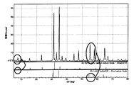
- FIG. 3 is an X-ray diffraction chart showing peaks A to K of oxide A.
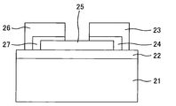
- FIG. FIG. 3 is a diagram illustrating an X-ray diffraction chart of oxide A, and crystal structures of InGaO 3 (ZnO) 2 (JCPDS: 40-0252) and In 2 O 3 (ZnO) 2 (JCPDS: 20-1442). It is a figure which shows the element structure of TFT produced in this Example 14.
- the thin film transistor (TFT) of the present invention uses, as an active layer, an oxide containing the elements In, Ga, and Zn in the following regions 1, 2, or 3 (atomic ratio).
- Region 1 0.58 ⁇ In / (In + Ga + Zn) ⁇ 0.68 0.15 ⁇ Ga / (In + Ga + Zn) ⁇ 0.29
- Region 2 0.45 ⁇ In / (In + Ga + Zn) ⁇ 0.58 0.09 ⁇ Ga / (In + Ga + Zn) ⁇ 0.20
- Region 3 0.45 ⁇ In / (In + Ga + Zn) ⁇ 0.58 0.20 ⁇ Ga / (In + Ga + Zn) ⁇ 0.27
- the thin film transistor of the present invention has a field effect mobility of 25 cm 2 / Vs or more.
- the atomic ratio of each element contained in the oxide that is the active layer is obtained by quantitatively analyzing the contained element by an inductively coupled plasma emission spectrometer (ICP-AES).
- ICP-AES inductively coupled plasma emission spectrometer
- this light shows a wavelength (spectral line) unique to the element
- the presence of the element can be confirmed by the presence or absence of the spectral line (qualitative analysis).
- the magnitude (luminescence intensity) of each spectral line is proportional to the number of elements in the sample
- the sample concentration can be obtained by comparing with a standard solution having a known concentration (quantitative analysis). After identifying the elements contained in the qualitative analysis, the content is obtained by quantitative analysis, and the atomic ratio of each element is obtained from the result.
- Field-effect mobility of the TFT of the present invention is preferably at least 25 cm 2 / Vs, preferably at least 28cm 2 / Vs, and particularly preferably equal to or greater than 30 cm 2 / Vs.
- a peripheral circuit such as a driver circuit can be formed on the panel in a small area.
- it is 30 cm 2 / Vs or more, since the TFT can be further reduced, application to a panel of a mobile device such as a smartphone or a tablet terminal can be expected.
- the higher the field effect mobility, the better, and the upper limit value is not particularly limited, but is considered to be, for example, about 100 cm 2 / Vs.
- Evaluation items of transistor characteristics include, for example, threshold voltage (Vth), On / Off ratio, S value, etc., in addition to field effect mobility.
- the field effect mobility can be obtained from the characteristics of the linear region and the saturation region.
- a method of deriving field-effect mobility by creating a graph of Id-Vg from the result of transfer characteristics and calculating Vg-transconductance (Gm) can be mentioned.
- Gm is represented by ⁇ (Id) / ⁇ (Vg).
- Id is the current between the source and drain electrodes
- Vg is the gate voltage when the voltage Vd is applied between the source and drain electrodes.
- the S value of the TFT of the present invention is preferably 0.6 (V / decade) or less, more preferably 0.5 (V / decade) or less, and particularly preferably an S value of 0.4 (V / decade) or less. If the S value is 0.6 (V / decade) or less, it can be expected to reduce power consumption during driving.
- the TFT normally controls the current Id between the source and drain electrodes by switching the gate voltage Vg between 0 V and 5 to 20 V when a voltage Vd of about 5 to 20 V is applied between the source and drain electrodes ( ON / OFF).
- the conditions for measuring the transfer characteristics of a TFT are usually as follows. Vg: -15V to 20V Vd: 0.1V, 1V, 10V
- the active layer of the TFT of the present invention can be manufactured using a sputtering target described below.
- the sputtering target is made of an oxide sintered body containing the elements In, Ga, and Zn in the range of atomic ratios of the following regions 1, 2, or 3.
- Region 1 0.58 ⁇ In / (In + Ga + Zn) ⁇ 0.68 0.15 ⁇ Ga / (In + Ga + Zn) ⁇ 0.29
- Region 2 0.45 ⁇ In / (In + Ga + Zn) ⁇ 0.58 0.09 ⁇ Ga / (In + Ga + Zn) ⁇ 0.20
- a TFT having a high mobility and a particularly small S value can be obtained.
- Ga is relatively large, a TFT having a short wavelength transmittance and a low photocurrent can be expected.
- the etching rate is close to that of an amorphous transparent electrode (indium zinc oxide or ITO) with respect to the oxalic acid-based etching solution, and the process design is easy.
- the region 1 is particularly preferably in the following range. 0.58 ⁇ In / (In + Ga + Zn) ⁇ 0.65 0.15 ⁇ Ga / (In + Ga + Zn) ⁇ 0.29 0.13 ⁇ Zn / (In + Ga + Zn)
- In / (In + Ga + Zn) is less than 0.65, the S value is easily reduced. Moreover, it is easy to be normally off.
- Ga / (In + Ga + Zn) exceeds 0.15, improvement in moisture resistance can be expected.
- Zn / (In + Ga + Zn) is 0.13 or more, it is easy to lower the specific resistance of the sintered body. In addition, when manufacturing a TFT, etching is easy and residue is not easily left.
- the region 2 is particularly preferably in the following range. 0.45 ⁇ In / (In + Ga + Zn) ⁇ 0.58 0.10 ⁇ Ga / (In + Ga + Zn) ⁇ 0.20
- In / (In + Ga + Zn) is 0.45 or more, high mobility can be expected.
- Ga / (In + Ga + Zn) is smaller than 0.20, normally-off operation is facilitated.
- the field effect mobility is slightly lower than those of the region 1 and the region 2, but a TFT having a small S value is obtained.
- the region 3 is more preferably in the following range. 0.45 ⁇ In / (In + Ga + Zn) ⁇ 0.58 0.20 ⁇ Ga / (In + Ga + Zn) ⁇ 0.25
- Ga / (In + Ga + Zn) is smaller than 0.25, the mobility is increased. If it is larger than 0.20, the transmittance of light having a short wavelength is increased, and a reduction in photocurrent can be expected.
- In / (In + Ga + Zn) is 0.45 or more, high mobility can be expected.
- the oxide sintered body constituting the sputtering target preferably has oxygen vacancies.
- the oxygen deficiency is preferably in the range of 1 ⁇ 10 ⁇ 7 to 3 ⁇ 10 ⁇ 1 times the oxygen atom content calculated from the composition ratio. If it is within the above range, the specific resistance can be easily lowered. It is more preferable that the oxygen deficiency of the target (sintered body) is 1 ⁇ 10 ⁇ 7 times or more and less than 1 ⁇ 10 ⁇ 3 times the stoichiometric ratio of oxygen atoms calculated from the composition ratio. Particularly preferred is less than 5 ⁇ 10 ⁇ 4 times.
- the threshold voltage is unlikely to become negative because there is sufficient oxygen activated when forming the semiconductor film.
- the amount of oxygen vacancies can be adjusted according to the sintering conditions, the atmosphere during sintering, the temperature rise, and the temperature drop. Moreover, it can also adjust by carrying out a reduction process after sintering. If an In-rich layer is provided, it is easy to adjust the oxygen deficiency within the above range without performing a reduction treatment after sintering.
- the amount of oxygen deficiency is a value obtained by subtracting the number of oxygen ions contained in one mole of oxide crystal from the number of stoichiometric oxygen ions in mole units.
- the number of oxygen ions contained in the oxide crystal can be calculated, for example, by measuring the amount of carbon dioxide produced by heating the oxide crystal in carbon powder using an infrared absorption spectrum.
- the number of stoichiometric oxygen ions can be calculated from the mass of the oxide crystal.
- the number of portions (ZnGa 2 O 4 compound, etc.) in which indium having a diameter of 3 ⁇ m or more is missing within the range of 90 ⁇ m ⁇ 90 ⁇ m is preferably 10 or less, and more preferably 5 or less. One or less is particularly preferred. Since the portion where indium is deficient tends to have high resistance, if the number is small, the occurrence of abnormal discharge can be expected to be reduced.
- EPMA electron beam microanalyzer
- EPMA can be measured under the following conditions. -Equipment: JEOL Ltd. JXA-8200 Measurement conditions: acceleration voltage: 15 kV, irradiation current: 50 nA, irradiation time (per point): 50 mS
- the oxide sintered body preferably has a nitrogen content of 5 ppm (atoms) or less.
- the nitrogen content of the oxide sintered body exceeds 5 ppm, there is a possibility that abnormal discharge during sputtering of the obtained target and the amount of adsorbed gas on the target surface may not be sufficiently suppressed.
- black indium nitride (InN) reacts during sputtering to be mixed into the semiconductor film and the yield is lowered.
- the nitrogen partial pressure during sintering is usually less than 1 atmosphere, preferably the nitrogen partial pressure is 0.8 atmospheres or less, more preferably the nitrogen partial pressure is 0.5 atmospheres or less, and particularly preferably Sinter in an oxygen atmosphere.
- the oxide sintered body preferably has a specific resistance of less than 15 m ⁇ cm and a relative density of more than 97%.
- the specific resistance is more preferably 10 m ⁇ cm or less, and particularly preferably 5 m ⁇ cm or less. Moreover, it is usually 0.1 m ⁇ cm or more.
- the specific resistance is less than 15 m ⁇ cm, the target is difficult to break even when AC sputtering is performed, and when the specific resistance is 10 m ⁇ cm or less, the target is difficult to break even when AC sputtering or DC sputtering is performed.
- the specific resistance is 15 m ⁇ cm or more, it is necessary to apply a high voltage when plasma discharge is performed by sputtering, which may change the fragment component during sputtering film formation and change the film quality.
- the specific resistance can be measured by the method described in this example.
- the relative density is more preferably 98% or more, and particularly preferably 99% or more. Also, it is usually less than 100%. When the relative density exceeds 97%, there are effects such as an increase in sputtering rate, an increase in strength and a difficulty in cracking.
- the relative density can be measured by the method described in this example.
- the sputtering target of the present invention contains a metal element other than the above-described In, Ga, Zn, for example, Sn, Ge, Si, Ti, Zr, Hf, etc., as long as the effects of the present invention are not impaired. Also good.
- the metal element contained in the target may be substantially only In, Ga, and Zn. Note that “substantially” means that no elements other than impurities, which are inevitably included due to raw materials, manufacturing processes, and the like are not included.
- the oxide sintered body constituting the sputtering target contains the elements In, Ga, and Zn in the range of the region 1, it is preferably represented by a homologous structure compound represented by (InGaO 3 ) ZnO and In 2 O 3 .
- a bixbite structure compound is preferably represented by (InGaO 3 ) ZnO and In 2 O 3 .
- XRD X-ray diffraction measurement
- m 1 of the crystal structure represented by InGaO 3 (ZnO) m (m is an integer of 1 to 20) is InGaO 3 (ZnO).
- a crystal structure represented by InGaO 3 (ZnO) m is called a “hexagonal layered compound” or a “crystal structure of a homologous phase”, and has a long period in which several crystal layers of different substances are stacked.
- a crystal having a “lattice” structure When the crystal cycle or thickness of each thin film layer is on the order of nanometers, depending on the combination of the chemical composition of these layers and the thickness of the layers, the properties differ from the properties of a single substance or a mixed crystal in which each layer is uniformly mixed. The following characteristics can be obtained.
- the crystal structure of the homologous phase can be confirmed, for example, because the X-ray diffraction pattern directly measured from the powder obtained by pulverizing the target or the target matches the crystal structure X-ray diffraction pattern of the homologous phase assumed from the composition ratio. Specifically, it can be confirmed from the coincidence with the crystal structure X-ray diffraction pattern of the homologous phase obtained from a JCPDS (Joint Committee of Powder Diffraction Standards) card. In the case of InGaO 3 (ZnO), JCPDS card no. 38-1104.
- JCPDS Joint Committee of Powder Diffraction Standards
- the bixbite structure (or rare earth oxide C-type crystal structure) represented by In 2 O 3 is a cubic system having a space group of (T h 7 , I a3 ), and Mn 2 O 3 (I) Also called type oxide crystal structure.
- JCPDS card no. The pattern of 6-0416 is shown. Sc 2 O 3 , Y 2 O 3 , Tl 2 O 3 , Pu 2 O 3 , Am 2 O 3 , Cm 2 O 3 , In 2 O 3 , ITO (In 2 O 3 doped with Sn of about 10 wt% or less ) Shows this crystal structure (Japan Society for the Promotion of Science, Transparent Oxide Optoelectronic Materials, No. 166, “Technology of Transparent Conductive Film”, Ohmsha).
- the crystal structure of the rare earth oxide C type is confirmed by X-ray diffraction according to JCPDS card No. This can be confirmed by showing the pattern of 6-0416.
- the crystal structure of the rare earth oxide C type has a stoichiometric ratio of M 2 X from a fluorite type crystal structure which is one of the crystal structures of a compound represented by MX 2 (M: cation, X: anion). 3 so that one out of four anions is missing.
- Anions usually oxygen in the case of oxides
- Anions are coordinated to cations, and the remaining two anion sites are empty. Empty anion sites are also called quasi-ion sites ("transparent conductive film technology").
- the rare earth oxide C-type crystal structure in which oxygen (anion) is coordinated to 6 positive ions (cations) has an oxygen octahedral ridge sharing structure. When the oxygen octahedral ridge sharing structure is used, the ns orbitals of the p metal, which is a cation, overlap each other to form an electron conduction path, and the effective mass is reduced to show high electron mobility.
- the crystal structure of the rare earth oxide C type is determined by X-ray diffraction according to JCPDS card No. If the 6-0416 pattern is shown, the stoichiometric ratio may deviate from M 2 X 3 . That is, it may be M 2 O 3-d .
- the incident angle (2 ⁇ ) is preferably A to E below by X-ray diffraction measurement (Cuk ⁇ ray).
- An oxide (oxide A) in which a diffraction peak is observed at each position is included (Condition 1).
- A. 2 ⁇ 7.0 ° to 8.4 ° (preferably 7.2 ° to 8.2 °)
- B. 2 ⁇ 30.6 ° -32.0 ° (preferably 30.8 ° -31.8 °)
- C. 2 ⁇ 33.8 ° to 35.8 ° (preferably 34.3 ° to 35.3 °)
- D. 2 ⁇ 53.5 ° to 56.5 ° (preferably 54.1 ° to 56.1 °)
- E. 2 ⁇ 56.5 ° to 59.5 ° (preferably 57.0 ° to 59.0 °)
- the oxide A satisfies the following condition 2.
- Condition 2 One of diffraction peaks observed at positions where 2 ⁇ is 30.6 ° to 32.0 ° (region B) and 33.8 ° to 35.8 ° (region C) is a main peak, The other is a sub peak.
- the main peak is the strongest peak (peak with the highest peak height) in the range of 2 ⁇ of 5 to 80 °, and the sub peak is the second strongest peak.
- Condition 3 In the chart obtained by X-ray diffraction measurement (Cuk ⁇ ray), diffraction peaks are observed in the following F to K regions.
- F. 2 ⁇ 14.8 ° to 16.2 ° (preferably 15.0 ° to 16.0 °)
- G. 2 ⁇ 22.3 ° to 24.3 ° (preferably 22.8 ° to 23.8 °)
- H. 2 ⁇ 32.2 ° to 34.2 ° (preferably 32.7 ° to 33.7 °)
- I. 2 ⁇ 43.1 ° to 46.1 ° (preferably 43.6 ° to 45.6 °)
- J. et al. 2 ⁇ 46.2 ° to 49.2 ° (preferably 46.7 ° to 48.7 °)
- K. 2 ⁇ 62.7 ° to 66.7 ° (preferably 63.7 ° to 65.7 °)
- FIG. 1 An example of the X-ray diffraction chart of the oxide is shown in FIG.
- a to K represent the above peak positions.
- the horizontal axis is 2 ⁇ , and the vertical axis is intensity.
- XRD can be performed by, for example, the apparatus and conditions described in this embodiment.
- FIG. 2 shows an X-ray diffraction chart of oxide A, a crystal structure represented by InGaO 3 (ZnO) 2 (JCPDS: 40-0252), and In 2 O 3 (ZnO) 2 (JCPDS: 20-1442).
- the crystal structure is shown.
- An X-ray diffraction chart of the crystal of the oxide A is represented by a crystal structure represented by InGaO 3 (ZnO) 2 (JCPDS: 40-0252) and In 2 O 3 (ZnO) 2 (JCPDS: 20-1442). Similar to crystal structure.
- FIG. 2 shows an X-ray diffraction chart of oxide A, a crystal structure represented by InGaO 3 (ZnO) 2 (JCPDS: 40-0252) and In 2 O 3 (ZnO) 2 (JCPDS: 20-1442).
- the oxide A has a peak peculiar to InGaO 3 (ZnO) 2 (a peak in the region A) and a peak peculiar to In 2 O 3 (ZnO) 2 (the peaks in the regions D and E).
- the oxide A has a new periodicity different from that of InGaO 3 (ZnO) 2 and In 2 O 3 (ZnO) 2 . That is, the oxide A is different from InGaO 3 (ZnO) 2 and In 2 O 3 (ZnO) 2 .
- this peak is between the main peaks of In 2 O 3 (ZnO) 2 and InGaO 3 (ZnO) 2 , that is, between 31 ° and 32 °. Therefore, it is shifted to a lower angle side than the main peak of InGaO 3 (ZnO) 2 (it seems that the interstitial distance is widened), and is higher than the main peak of In 2 O 3 (ZnO) 2. There is a shift (it seems that the distance between lattices is narrowed).
- the crystal structure represented by In 2 O 3 (ZnO) m is a structure in which an InO 1.5 layer, an InZnO 2.5 layer, and a ZnO layer are periodically repeated at a ratio of 1: 1: (m ⁇ 1). It is considered to have In addition, the crystal structure represented by InGaO 3 (ZnO) m is considered that the InO 1.5 layer, the GaZnO 2.5 layer, and the ZnO layer are periodically repeated at a ratio of 1: 1: (m ⁇ 1). It has been.
- the crystal structure represented by In 2 O 3 (ZnO) m and the measurement results by X-ray diffraction of InGaO 3 (ZnO) m have different peak positions (differing interstitial distances) but similar patterns. It will be a thing.
- the crystal structure of the oxide A is a crystal composed of a “hexagonal layered compound” or a “crystal structure of a homologous phase” as in the case of In 2 O 3 (ZnO) m and InGaO 3 (ZnO) m described above. Presumed.
- the X-ray diffraction pattern of the crystal structure of the oxide A is particularly similar to that of In 2 O 3 (ZnO) 2 .
- ZnO In 2 O 3
- the crystal structure of oxide A can be sintered at a low temperature of 1550 ° C. or lower, and is considered to be a new crystal structure from the generation temperature.
- oxide A if the characteristic diffraction pattern of the above condition 1 or conditions 1 and 2 is shown by X-ray diffraction measurement, oxygen in the oxide is excessive or insufficient (oxygen deficiency). It does not matter (the atomic ratio of oxygen element may deviate from the stoichiometric ratio). If the oxygen in the oxide is excessive, the resistance may be too high when the target is used, and therefore it is preferable that the oxide has oxygen vacancies.
- the oxide sintered body constituting the sputtering target includes the elements In, Ga, and Zn in the range of the region 3, the oxide sintered body preferably includes a homologous structure compound represented by (InGaO 3 ) ZnO.
- a high-performance TFT (high mobility, low S value) can be manufactured by parallel plate type sputtering widely used industrially.
- the compounding step is a step of mixing a metal oxide that is a raw material of the sputtering target.
- powders such as indium compound powder, gallium compound powder, and zinc compound powder are used.
- the specific surface area (BET specific surface area) of each metal compound as a target raw material can be measured by the method described in JIS Z 8830.
- the indium compound include indium oxide and indium hydroxide.
- the gallium compound include gallium oxide and gallium hydroxide.
- the zinc compound include zinc oxide and zinc hydroxide.
- an oxide is preferable because it is easy to sinter and it is difficult to leave a by-product.
- the purity of the raw material is usually 2N (99% by mass) or more, preferably 3N (99.9% by mass) or more, particularly preferably 4N (99.99% by mass) or more.
- the purity is lower than 2N, the durability is deteriorated.
- impurities may enter the liquid crystal side and burning may occur.
- metallic zinc zinc powder
- zinc powder is used as a part of the raw material, the generation of white spots can be reduced.
- the mixing and grinding time is usually 0.5 to 60 hours, preferably 6 to 48 hours, more preferably 8 to 36 hours. If it is less than 0.5 hours, there is a risk of poor appearance such as white spots and black spots due to poor dispersion of raw materials. If it is longer than 60 hours, there is a possibility that an unexpected crystal form may be formed by reaction during mixing.
- the specific surface area (BET specific surface area) of indium oxide, gallium oxide, and zinc oxide is usually 3 to 18 m 2 / g, 3 to 18 m 2 / g, and 3 to 18 m 2 / g, respectively, preferably 7 to 16 m 2. / G, 7 to 16 m 2 / g, 3 to 10 m 2 / g, more preferably 7 to 15 m 2 / g, 7 to 15 m 2 / g, and 4 to 10 m 2 / g, particularly preferably each. 11 to 15 m 2 / g, 11 to 15 m 2 / g, and 4 to 5 m 2 / g.
- the specific surface area is too small, aggregates of the respective elements may grow in the sintered body, the crystal form of the raw material powder may remain, an unexpected crystal form may be generated, and the properties may change. If the specific surface area is too large, an unexpected crystal form may be generated and the properties may be changed, or a dispersion failure may occur, resulting in poor appearance or uneven characteristics.
- the calcination process is a process provided as necessary, after obtaining a mixture of compounds that are raw materials of the sputtering target, and then calcining the mixture.
- the metal oxide mixture is preferably heat-treated at 500 to 1200 ° C. for 1 to 100 hours. This is because the thermal decomposition of the indium compound, the zinc compound, and the tin compound may be insufficient under heat treatment conditions of less than 500 ° C. or less than 1 hour.
- the heat treatment condition exceeds 1200 ° C. or exceeds 100 hours, coarsening of the particles may occur. Therefore, it is particularly preferable to perform heat treatment (calcination) in the temperature range of 800 to 1200 ° C. for 2 to 50 hours.
- the calcined product obtained here is preferably pulverized before the following molding step and firing step.
- the molding step is a step of pressure-molding a mixture of metal oxides (or calcined product when the calcining step is provided) to form a compact. By this process, it is formed into a shape suitable as a target.
- the obtained calcined fine powder can be granulated and then molded into a desired shape by pressure molding.
- the molding method that can be used in this step include mold molding, cast molding, injection molding, and the like, and a homogeneous sintered body (target) having a high sintering density and a low specific resistance is obtained.
- molding aids such as polyvinyl alcohol, methylcellulose, polywax, and oleic acid may be used.
- the thickness of the molded body is usually 6 mm or more, preferably 8 mm or more, particularly preferably 10 mm or more. If it is less than 6 mm, it shrinks at the time of sintering and becomes too thin, resulting in uneven thermal conductivity, resulting in the formation of an unexpected crystal form, and the crystal grain size may become too large.
- a sintering process is an essential process of baking the molded object obtained at the said formation process.
- it is preferably performed under an oxygen-containing atmosphere, an oxygen gas atmosphere, or an oxygen gas pressurization.
- the heating rate during sintering is usually 4 ° C./min or less, preferably 3 ° C./min or less. If it is 4 ° C./min or less, cracks are unlikely to occur. Furthermore, the rate of temperature rise is 2.5 ° C./min or less between room temperature and 400 ° C., 2.5 ° C./min or less between 400 ° C. and 800 ° C., and 1.0 ° C. between 800 ° C. and sintering temperature. It is preferable that it is below °C / min.
- the temperature rising rate between room temperature and 400 ° C. is more preferably 1.0 ° C./min or less. If the temperature rising rate between room temperature and 400 ° C.
- the rate of temperature increase between 800 ° C. and the sintering temperature is more preferably 0.9 ° C./min or less. If the rate of temperature increase between 800 ° C. and the sintering temperature is 0.9 ° C./min or less, the crystal form of the present invention is likely to occur.
- Sintering is usually performed at 1100 to 1600 ° C. for 1 to 100 hours. It is preferable to carry out at 1300 to 1450 ° C. for 6 to 48 hours.
- oxide A is easily generated according to the following sintering method.
- the temperature is raised between 400 ° C. and 1000 ° C. at 2.5 ° C./min or less, and sintering is performed at 1350 to 1400 ° C. for 20 to 48 hours. Increase the temperature between 400 ° C. and 1000 ° C. at 2.5 ° C./min or less and sinter at 1400-1490 ° C. for 6 to 20 hours, or between 400 ° C. and 1000 ° C. at 2.5 ° C./min or less The temperature is raised and sintering is performed at 1490 to 1650 ° C. for 2 to 6 hours. Further, it is preferable that the temperature between 800 and the sintering temperature is raised at 1.0 ° C./min or less, the sintering temperature is 1350 to 1500 ° C., and the sintering time is 6 to 24 hours.
- the cooling rate during sintering is usually 4 ° C./min or less, preferably 2 ° C./min or less, more preferably 1 ° C./min or less, further preferably 0.8 ° C./min or less, particularly preferably 0.5 ° C. / Min or less.
- the crystal form of this invention is easy to be obtained as it is 4 degrees C / min or less. In addition, cracks are unlikely to occur when the temperature drops. Alternatively, the temperature rise may be stopped once during the temperature rise and held at the holding temperature, and sintering may be performed in two or more stages.
- the lower limit value of the temperature raising rate and the temperature lowering rate at the time of sintering is not particularly limited, but is preferably 0.1 ° C./min or more in consideration of productivity. In the case of a temperature increase / decrease rate below this, since the sintering time in production exceeds 500 hours, productivity is remarkably deteriorated and control becomes difficult.
- Reduction process is a process provided as needed which performs a reduction process in order to reduce the bulk resistance of the sintered compact obtained at the said sintering process as the whole target.
- the reduction method that can be applied in this step include a method using a reducing gas, vacuum firing, or reduction using an inert gas.
- a reducing gas hydrogen, methane, carbon monoxide, a mixed gas of these gases and oxygen, or the like can be used.
- reduction treatment by firing in an inert gas nitrogen, argon, a mixed gas of these gases and oxygen, or the like can be used.
- the oxygen deficiency amount of the target (sintered body) is desired to be a predetermined amount or less, it is preferable not to perform the reduction treatment after sintering.
- the processing step is to cut the sintered body obtained by sintering as described above into a shape suitable for mounting on a sputtering apparatus, and to mount a jig such as a backing plate. It is the process provided as needed for attaching.
- the thickness of the sintered body before grinding is preferably 5.5 mm or more, more preferably 6 mm or more, and particularly preferably 8 mm or more.
- the grinding is usually 0.2 mm or more on one side, preferably 0.5 mm or more, more preferably 2 mm or more. There is an advantage that a homogeneous target can be produced by producing a thick sintered body and grinding it sufficiently.
- the sintered body is ground with, for example, a surface grinder to obtain a material having a surface roughness (Ra) of 5 ⁇ m or less.
- the sputtering surface of the sputtering target may be further mirror-finished so that the average surface roughness (Ra) is 1000 angstroms or less.
- a known polishing technique such as mechanical polishing, chemical polishing, mechanochemical polishing (a combination of mechanical polishing and chemical polishing) can be used.
- polishing to # 2000 or more with a fixed abrasive polisher polishing liquid: water
- lapping with loose abrasive lapping abrasive: SiC paste, etc.
- lapping by changing the abrasive to diamond paste can be obtained by:
- Such a polishing method is not particularly limited.
- the obtained sputtering target material is bonded to a backing plate.
- the thickness of the target is usually 2 to 20 mm, preferably 3 to 12 mm, particularly preferably 4 to 10 mm.
- a plurality of targets may be attached to one backing plate to substantially serve as one target.
- the surface is preferably finished with a 200 to 10,000 diamond grindstone, and particularly preferably with a 400 to 5,000 diamond grindstone. If a diamond grindstone smaller than No. 200 or larger than 10,000 is used, the target may be easily broken. It is preferable that the target has a surface roughness Ra ⁇ 0.5 ⁇ m and has a ground surface with no directivity. If Ra is larger than 0.5 ⁇ m or the polished surface has directivity, abnormal discharge may occur or particles may be generated.
- air blow or running water cleaning can be used for the cleaning process.
- air blow or running water cleaning can also be performed.
- This ultrasonic cleaning is effective by performing multiple oscillations at a frequency of 25 to 300 KHz.
- it is preferable to perform ultrasonic cleaning by multiplying twelve types of frequencies in 25 KHz increments between frequencies of 25 to 300 KHz.
- glass substrates such as alkali silicate glass, alkali-free glass and quartz glass, silicon substrates, resin substrates such as acrylic, polycarbonate and polyethylene naphthalate (PEN), polymer film bases such as polyethylene terephthalate (PET) and polyamide Materials can be used.
- PEN polyethylene naphthalate
- PET polyethylene terephthalate
- the semiconductor layer (also referred to as a channel layer or an active layer) is preferably an amorphous film.
- an amorphous film By being an amorphous film, adhesion with an insulating film and a protective layer can be improved, and uniform transistor characteristics can be easily obtained even in a large area.
- whether or not the semiconductor layer is an amorphous film can be confirmed by X-ray crystal structure analysis. The case where no clear peak is observed is amorphous.
- the film thickness is usually 5 to 200 nm, preferably 20 to 150 nm, more preferably 30 to 100 nm. If the thickness is 5 nm or more, reproducibility of characteristics can be expected. If it is 200 nm or less, it can be manufactured with a tact time (time required for one process for each sheet) that can be economically adopted when manufacturing a large display. In order to obtain high mobility, the thickness is particularly preferably 100 nm or less. Moreover, when producing on a large substrate exceeding 2 m as in the production of a large liquid crystal display, it is particularly preferable to exceed 30 nm in order to ensure in-plane uniformity.
- the channel length (L) is preferably 1 to 50 ⁇ m, more preferably 3 to 40 ⁇ m, and particularly preferably 5 to 25 ⁇ m. If it exceeds 50 ⁇ m, the size of the transistor becomes too large and the degree of integration may decrease. When the thickness is less than 1 ⁇ m, high accuracy is required for photolithography, which may make it difficult to employ in a large area display or the like.
- the channel width (W) is preferably 1 to 500 ⁇ m, more preferably 3 to 100 ⁇ m, and particularly preferably 5 to 50 ⁇ m. If it exceeds 500 ⁇ m, the transistors may become too large and the integration degree may decrease.
- W / L which is the ratio of the channel width (W) to the channel length (L), is usually 0.1 to 10, preferably 0.5 to 5. Within the above range, the panel design is easy.
- the TFT of the present invention may have a channel layer protective layer.
- the material for forming the protective layer of the channel layer is not particularly limited. What is generally used can be arbitrarily selected as long as the effects of the present invention are not lost.
- An oxide such as Y 2 O 3 , Hf 2 O 3 , CaHfO 3 , PbTi 3 , BaTa 2 O 6 , SrTiO 3, or AlN can be used.
- the number of oxygen in these oxides does not necessarily match the stoichiometric ratio (for example, it may be SiO 2 or SiO x ).
- SiN x may contain a hydrogen element.
- Such a protective film may have a structure in which two or more different insulating films are stacked.
- the gate insulating film is usually made of a dielectric material having a relative dielectric constant of 2 to 10.
- the relative dielectric constant of the gate insulating film is preferably in the range of 2.5 to 10, more preferably in the range of 3 to 6.
- the relative dielectric constant of the gate insulating film can be measured by a dielectric constant measuring apparatus.
- the relative dielectric constant is a dimensionless quantity and takes a constant value regardless of the unit system used.
- the dielectric material having a relative dielectric constant of 2 to 9 SiO 2 , SiN x , SiON, Al 2 O 3 and the like are preferable because they have a high industrial track record and can be applied to a large area.
- SiO 2 and SiN x are preferable because they can be easily applied to displays.
- the number of oxygen in the oxide that is the dielectric material does not necessarily match the stoichiometric ratio (for example, it may be SiO 2 or SiO x ).
- SiN x may contain a hydrogen element.
- the gate insulating film of the field effect transistor of the present invention may have a structure in which two or more different insulating films are stacked.
- the gate insulating film may be crystalline, polycrystalline, or amorphous, but is preferably polycrystalline or amorphous that is easy to manufacture industrially.
- the gate insulating film made of a dielectric material having a relative dielectric constant of 2 to 9 is thermally oxidized, and the surface of the silicon substrate is thermally oxidized (made of SiOx). Layer).
- the gate insulating film can be formed by depositing SiN x and / or SiO x with a plasma enhanced chemical vapor deposition apparatus (PECVD), for example.
- PECVD plasma enhanced chemical vapor deposition apparatus
- SiOx and SiNx, and laminated films and mixed films thereof have a track record of industrialization in a large area, and are more preferable because they can be produced inexpensively and uniformly.
- each of the gate electrode, the source electrode, and the drain electrode there are no particular limitations on the material for forming each of the gate electrode, the source electrode, and the drain electrode, and any material generally used can be selected as long as the effects of the present invention are not lost.
- transparent electrodes such as indium tin oxide (ITO), indium zinc oxide, ZnO, SnO 2 , metal electrodes such as Al, Ag, Cr, Ni, Mo, Au, Ti, Ta, Cu, or these An alloy metal electrode can be used.
- Each constituent member (layer) of the TFT can be formed by a method known in this technical field.
- a film formation method a chemical film formation method such as a spray method, a dip method, or a CVD method, or a physical formation method such as a sputtering method, a vacuum evaporation method, an ion plating method, a pulse laser deposition method, or the like.
- a membrane method can be used. It is preferable to use a physical film forming method because the carrier density is easy to control and the film quality can be easily improved. Among them, it is more preferable to use the sputtering method because of high productivity.
- the formed film can be patterned by various etching methods.
- the channel layer (semiconductor layer) of the TFT of the present invention is preferably formed by forming a film by DC or AC sputtering using the sputtering target of the present invention.
- DC or AC sputtering damage during film formation can be reduced as compared with RF sputtering. For this reason, when it is set as TFT, effects, such as a mobility improvement, can be anticipated.
- the target of the present invention since the specific resistance is small and the density is high, troubles such as generation of cracks hardly occur even when the film is formed by DC or AC sputtering.
- the channel layer it is preferable to include a channel layer oxidation treatment step.
- the oxidation treatment include the following. -Oxygen partial pressure at the time of sputtering shall be 0.1 Pa or more.
- a heat treatment oxygen annealing
- -Film formation is performed in an oxygen plasma atmosphere (oxygen plasma treatment).
- heat treatment is preferably performed at 70 to 350 ° C. If it is lower than 70 ° C., the thermal stability and heat resistance of the obtained transistor may be lowered, the mobility may be lowered, the S value may be increased, or the threshold voltage may be increased. On the other hand, when the temperature is higher than 350 ° C., a substrate having no heat resistance cannot be used, and there is a possibility that equipment costs for heat treatment may be required.
- the heat treatment is preferably performed in an inert gas or in the presence of oxygen.
- CIP cold isostatic pressing
- the obtained molded body was sintered under the following conditions.
- Sintering atmosphere Oxygen heating rate (room temperature to 400 ° C): 0.5 ° C / min heating rate (400 ° C to switching temperature): 1.0 ° C / min switching temperature: 800 ° C
- Temperature increase rate (switching temperature to sintering temperature): 0.3 ° C./min
- Sintering temperature 1400 ° C.
- Sintering time 24 hours
- Cooling rate (sintering temperature to room temperature): 0.3 ° C./min Heat treatment (reduction treatment) under reducing conditions was not performed.
- a sintered body having a thickness of 8 mm was ground and polished on both sides to a thickness of 6 mm to obtain a target material having a diameter of 2 inches.
- the nitrogen content in the sintered body was measured with a trace total nitrogen analyzer (TN).
- the nitrogen content of the sintered body was 5 ppm or less.
- the trace total nitrogen analyzer (TN) uses only nitrogen (N) or only nitrogen (N) and carbon (C) as element elements in elemental analysis, and determines the amount of nitrogen, or the amount of nitrogen and carbon. Used for analysis.
- nitrogen-containing inorganic substances or nitrogen-containing organic substances are decomposed in the presence of a catalyst, N is converted into nitrogen monoxide (NO), this NO gas is reacted with ozone in a gas phase, light is emitted by chemiluminescence, and the light emission. N is determined from the intensity.
- the surface of the sintered body was blown with air and further subjected to ultrasonic cleaning for 3 minutes, and then bonded to an oxygen-free copper backing plate with indium solder to obtain a target.
- TFT Thin Film Transistor
- a mask for forming source and drain electrodes was attached and Au was deposited by RF sputtering to form source and drain electrodes. After that, heat treatment was performed in the atmosphere at 300 ° C. for 60 minutes to obtain a transistor having a channel length of 100 ⁇ m and a channel width of 2000 ⁇ m.
- the elemental composition ratio (atomic ratio) of the channel layer was measured by ICP-AES.
- a semiconductor parameter analyzer Karlin, Inc .: 4200SCS
- a manual prober EP-6 or PM-5, manufactured by SUSS Microtec Co., Ltd.
- the transfer characteristics of the TFT are measured to determine the mobility (field effect mobility ( ⁇ ) and S values were evaluated.
- the TFT was heated at 110 ° C. with a hot plate until immediately before the measurement.
- Example 2 to 13 Comparative Examples 1 and 2 A target was fabricated and evaluated in the same manner as in Example 1 except that the atomic ratio of the target was changed as shown in Table 1, and a TFT was fabricated and evaluated. In any case, the nitrogen content of the sintered body (target) was 5 ppm or less. The results are shown in Table 1.
- Comparative Examples 3-5 Using three targets of In 2 O 3 , ZnO, and Ga 2 O 3 , an oxide film was formed by adjusting the power of each cathode so as to have the atomic composition ratio shown in Table 2 by co-sputtering by RF sputtering. As an active layer, TFTs were fabricated and evaluated under the conditions shown in Table 2. Other operations were performed in the same manner as in Example 1. The results are shown in Table 2.
- Example 14 Using the sputtering target produced in Example 1, a bottom gate / top contact type TFT was produced and evaluated by the following method.
- the element structure of the bottom gate / top contact type TFT is shown in FIG. Specifically, after forming the oxide film 25 on the Si substrate 21 with the thermal oxide film 22 using the sputtering target, patterning, electrode formation, and the like were performed to form an element.
- the structure of the element is a bottom gate / top contact type.
- the gate electrode 21 is n + -Si
- the insulating film 22 is SiO 2
- the source / drain electrodes 24, 27, 23, 26 are stacked with Ti 23, 26 and Au 24, 27. Used the body.
- the channel width and channel length were 150 ⁇ m and 10 ⁇ m, respectively, and the film thickness of the active layer 25 was 40 nm.
- the produced TFT was evaluated in the same manner as in Example 1. The results are shown in Table 2.
- Example 15 A TFT was produced and evaluated in the same manner as in Example 14 except that the target produced in Example 8 was used. The results are shown in Table 2.
- Example 16 A TFT was produced and evaluated in the same manner as in Example 14 except that the target produced in Example 12 was used. The results are shown in Table 2.
- Example 17 Using the target of Example 1, using photolithography (lift-off), SiO 2 as the gate insulating film, Ti / Au as the source and drain electrodes, and 100 nm SiO 2 produced by PECVD as the protective film, channel length 20 ⁇ m, channel width 10 ⁇ m Transistor was obtained. The TFT was evaluated in the same manner as in Example 1. The results are shown in Table 2.
- Example 18 A TFT was fabricated and evaluated in the same manner as in Example 17 except that the oxygen partial pressure was lowered and instead an oxidation treatment was performed by high-pressure oxygen annealing at 10 atm, 250 ° C. for 1 hour in an oxygen atmosphere after TFT fabrication. . The results are shown in Table 2.
- the thin film transistor of the present invention can be used for a display device, particularly for a large area display.
Landscapes
- Chemical & Material Sciences (AREA)
- Engineering & Computer Science (AREA)
- Ceramic Engineering (AREA)
- Materials Engineering (AREA)
- Organic Chemistry (AREA)
- Manufacturing & Machinery (AREA)
- Structural Engineering (AREA)
- Mechanical Engineering (AREA)
- Chemical Kinetics & Catalysis (AREA)
- Metallurgy (AREA)
- Inorganic Chemistry (AREA)
- Physics & Mathematics (AREA)
- Thermal Sciences (AREA)
- Thin Film Transistor (AREA)
- Physical Vapour Deposition (AREA)
- Physical Deposition Of Substances That Are Components Of Semiconductor Devices (AREA)
- Compositions Of Oxide Ceramics (AREA)
Abstract
Description
当初、次世代ディスプレイ用TFTの移動度は、2~8cm2/Vs程度が目標といわれていたが、最近では20cm2/Vs以上、25cm2/Vs以上、さらに30cm2/Vs以上の移動度が期待されている(非特許文献1)。
しかし、前述したようにコスパッタで組成比を変えても30cm2/Vs前後の高い移動度のTFTを作製するには到っていなかった。
コスパッタ法では、基板に対して粒子が斜入射で成膜される点や、S-T間距離(基板とスパッタリングターゲット間の距離)が長い点等が平行平板型のスパッタ法とは異なり、基板に飛来するスパッタ粒子の成分やエネルギーが異なると考えられる。このことが、膜構造や膜質の違い、ひいてはTFT特性の違いに繋がっているものと推定される。
本発明によれば、以下の薄膜トランジスタ等が提供される。
1.元素In,Ga及びZnを下記領域1、2又は3の原子比の範囲で含む酸化物を活性層とし、電界効果移動度が25cm2/Vs以上である薄膜トランジスタ。
領域1
0.58≦In/(In+Ga+Zn)≦0.68
0.15<Ga/(In+Ga+Zn)≦0.29
領域2
0.45≦In/(In+Ga+Zn)<0.58
0.09≦Ga/(In+Ga+Zn)<0.20
領域3
0.45≦In/(In+Ga+Zn)<0.58
0.20≦Ga/(In+Ga+Zn)≦0.27
2.電界効果移動度が30cm2/Vs以上である1に記載の薄膜トランジスタ。
3.元素In,Ga及びZnを下記領域1、2又は3の原子比の範囲で含む酸化物焼結体からなるスパッタリングターゲット。
領域1
0.58≦In/(In+Ga+Zn)≦0.68
0.15<Ga/(In+Ga+Zn)≦0.29
領域2
0.45≦In/(In+Ga+Zn)<0.58
0.09≦Ga/(In+Ga+Zn)<0.20
領域3
0.45≦In/(In+Ga+Zn)<0.58
0.20≦Ga/(In+Ga+Zn)≦0.27
4.前記酸化物焼結体が、比抵抗15mΩcm未満、相対密度97%超である3に記載のスパッタリングターゲット。
5.前記酸化物焼結体が、元素In,Ga及びZnを前記領域1の原子比の範囲で含み、(InGaO3)ZnOで表されるホモロガス構造化合物と、In2O3で表されるビックスバイト構造化合物とを含む、3又は4に記載のスパッタリングターゲット。
6.前記酸化物焼結体が、元素In,Ga及びZnを前記領域2の原子比の範囲で含み、X線回折測定(Cukα線)により入射角(2θ)が、7.0°~8.4°、30.6°~32.0°、33.8°~35.8°、53.5°~56.5°及び56.5°~59.5°の各位置に回折ピークが観測される酸化物を含む、3又は4に記載のスパッタリングターゲット。
7.前記酸化物焼結体が、元素In,Ga及びZnを前記領域3の原子比の範囲で含み、(InGaO3)ZnOで表されるホモロガス構造化合物を含む、3又は4に記載のスパッタリングターゲット。
8.400℃~800℃の間を2.5℃/分以下で昇温する工程、
800℃~焼結温度の間を1.0℃/分以下で昇温する工程、及び
焼結温度1300~1450℃、焼結時間6~48時間で焼結する工程を含む3~7のいずれかに記載のスパッタリングターゲットの製造方法。
9.3~7のいずれかに記載のスパッタリングターゲットを用いて酸化物薄膜を作製する工程を含む1又は2に記載の薄膜トランジスタの製造方法。
領域1
0.58≦In/(In+Ga+Zn)≦0.68
0.15<Ga/(In+Ga+Zn)≦0.29
領域2
0.45≦In/(In+Ga+Zn)<0.58
0.09≦Ga/(In+Ga+Zn)<0.20
領域3
0.45≦In/(In+Ga+Zn)<0.58
0.20≦Ga/(In+Ga+Zn)≦0.27
また、本発明の薄膜トランジスタは電界効果移動度が25cm2/Vs以上である。
ICP-AES分析を具体的に説明する。溶液試料をネブライザーで霧状にして、アルゴンプラズマ(約6000~8000℃)に導入すると、試料中の元素は熱エネルギーを吸収して励起され、軌道電子が基底状態から高いエネルギー準位の軌道に移る。この軌道電子は10-7~10-8秒程度で、より低いエネルギー準位の軌道に移る。この際にエネルギーの差を光として放射し発光する。この光は元素固有の波長(スペクトル線)を示すため、スペクトル線の有無により元素の存在を確認できる(定性分析)。
また、それぞれのスペクトル線の大きさ(発光強度)は試料中の元素数に比例するため、既知濃度の標準液と比較することで試料濃度を求めることができる(定量分析)。
定性分析で含有されている元素を特定後、定量分析で含有量を求め、その結果から各元素の原子比を求める。
電界効果移動度が25cm2/Vs以上であると、パネル上にドライバー回路等の周辺回路を小さい面積の中に構成することができる。30cm2/Vs以上であると、さらにTFTを小さくできるため、スマートフォンやタブレット端末等のモバイル用機器のパネルへの応用も期待できる。
尚、電界効果移動度は高いほどよく、その上限値は特に限定しないが、例えば、100cm2/Vs程度であると考えられる。
電界効果移動度は、線形領域や飽和領域の特性から求めることができる。例えば線形領域においては、トランスファー特性の結果からId-Vgのグラフを作成し、Vg-トランスコンダクタンス(Gm)を算出することにより電界効果移動度を導く方法が挙げられる。尚、Gmは∂(Id)/∂(Vg)によって表される。本発明において特に断らない限り、電界効果移動度はこの方法で評価する。上記Idはソース・ドレイン電極間の電流、Vgはソース・ドレイン電極間に電圧Vdを印加したときのゲート電圧である。
S値についてはlogId-Vgのグラフを作成しId=10-10A~10-9Aの傾きから∂(Vg)/∂(logId)によって決める方法が挙げられる。
本発明のTFTのS値は、0.6(V/decade)以下が好ましく、0.5(V/decade)以下がより好ましく、S値0.4(V/decade)以下が特に好ましい。S値が0.6(V/decade)以下だと駆動時の消費電力を低減することが期待できる。
TFTのトランスファー特性を測定する際の条件は、通常次の通りとする。
Vg:-15V~20V
Vd:0.1V、1V、10V
スパッタリングターゲットは、元素In,Ga及びZnを下記領域1、2又は3の原子比の範囲で含む酸化物焼結体からなる。
領域1
0.58≦In/(In+Ga+Zn)≦0.68
0.15<Ga/(In+Ga+Zn)≦0.29
領域2
0.45≦In/(In+Ga+Zn)<0.58
0.09≦Ga/(In+Ga+Zn)<0.20
領域3
0.45≦In/(In+Ga+Zn)<0.58
0.20≦Ga/(In+Ga+Zn)≦0.27
0.58≦In/(In+Ga+Zn)<0.65
0.15<Ga/(In+Ga+Zn)≦0.29
0.13≦Zn/(In+Ga+Zn)
In/(In+Ga+Zn)を0.65未満とすると、S値を低減させやすい。また、ノーマリーオフとしやすい。Ga/(In+Ga+Zn)を0.15超とすると、耐湿性の向上が期待できる。Zn/(In+Ga+Zn)が0.13以上であると、焼結体の比抵抗を下げやすい。また、TFTを作製する際にエッチングが容易で残渣が残りにくい。
0.45≦In/(In+Ga+Zn)<0.58
0.10≦Ga/(In+Ga+Zn)<0.20
In/(In+Ga+Zn)が0.45以上だと高い移動度が期待できる。
Ga/(In+Ga+Zn)が0.20より小さいとノーマリーオフ動作が容易になる。
0.45≦In/(In+Ga+Zn)<0.58
0.20<Ga/(In+Ga+Zn)<0.25
Ga/(In+Ga+Zn)が0.25より小さいと移動度が高くなる。0.20より大きいと短波長の光の透過率が高くなり光電流の低減が期待できる。
In/(In+Ga+Zn)が0.45以上だと高い移動度が期待できる。
ターゲット(焼結体)の酸素欠損量が、組成比から計算した酸素原子の化学量論比の1×10⁻⁷倍以上、1×10⁻³倍未満であるものがより好ましい。5×10⁻⁴倍未満であるものが特に好ましい。1×10⁻³倍未満であると、半導体膜を成膜する際に活性化された酸素が十分あるため閾値電圧が負になりにくいことが期待できる。
ターゲット(焼結体)の酸素欠損量を上記範囲とするには、焼結後の還元処理を行なわないことが好ましい。また、焼結は窒素雰囲気で行なわず、大気雰囲気、あるいは酸素雰囲気で行なうことが好ましい。
EPMAは下記条件で測定することができる。
・装置:日本電子株式会社JXA-8200
・測定条件:加速電圧:15kV、照射電流:50nA、照射時間(1点当り):50mS
窒素含有量を上記とするには、通常焼結時の窒素分圧を1気圧未満、好ましくは窒素分圧0.8気圧以下、より好ましくは窒素分圧0.5気圧以下とし、特に好ましくは酸素雰囲気下で焼結する。
比抵抗は10mΩcm以下がより好ましく、5mΩcm以下が特に好ましい。また、通常は0.1mΩcm以上である。比抵抗が15mΩcm未満であると、ACスパッタリングした際でもターゲットが割れにくく、10mΩcm以下であるとACスパッタリングやDCスパッタリングした際でもターゲットが割れにくい。
また、比抵抗が15mΩcm以上であると、スパッタリングでプラズマ放電させる際に高い電圧を掛ける必要があり、スパッタリング成膜時のフラグメント成分が変化し、膜質が変化するおそれがある。比抵抗は本実施例に記載の方法で測定できる。
結晶周期又は各薄膜層の厚さがナノメーター程度の場合、これら各層の化学組成や層の厚さの組み合わせによって、単一の物質あるいは各層を均一に混ぜ合わせた混晶の性質とは異なる固有の特性が得られる。
希土類酸化物C型の結晶構造を示すことは、X線回折でJCPDSカードNo.6-0416のパターンを示すことから確認できる。
陽イオンに酸素(陰イオン)が6配位した希土類酸化物C型の結晶構造は、酸素8面体稜共有構造を有している。酸素8面体稜共有構造を有していると、陽イオンであるp金属のns軌道が互いに重なり合って電子の伝導路を形成し、有効質量が小さくなり高い電子の移動度を示す。
A.2θ=7.0°~8.4°(好ましくは7.2°~8.2°)
B.2θ=30.6°~32.0°(好ましくは30.8°~31.8°)
C.2θ=33.8°~35.8°(好ましくは34.3°~35.3°)
D.2θ=53.5°~56.5°(好ましくは54.1°~56.1°)
E.2θ=56.5°~59.5°(好ましくは57.0°~59.0°)
条件2:2θが30.6°~32.0°(上記領域B)及び33.8°~35.8°(上記領域C)の位置に観測される回折ピークの一方がメインピークであり、他方がサブピークである。メインピークとは、2θが5~80°の範囲で最も強度の強いピーク(ピーク高さの高いピーク)であり、サブピークとは、2番目に強度の強いピークである。
条件3:X線回折測定(Cukα線)により得られるチャートにおいて、下記F~Kの領域に回折ピークが観測される。
F.2θ=14.8°~16.2°(好ましくは15.0°~16.0°)
G.2θ=22.3°~24.3°(好ましくは22.8°~23.8°)
H.2θ=32.2°~34.2°(好ましくは32.7°~33.7°)
I.2θ=43.1°~46.1°(好ましくは43.6°~45.6°)
J.2θ=46.2°~49.2°(好ましくは46.7°~48.7°)
K.2θ=62.7°~66.7°(好ましくは63.7°~65.7°)
図2に、酸化物AのX線回折チャート、InGaO3(ZnO)2(JCPDS:40-0252)で示される結晶構造及びIn2O3(ZnO)2(JCPDS:20-1442)で示される結晶構造を示す。
酸化物Aの結晶のX線回折チャートは、InGaO3(ZnO)2(JCPDS:40-0252)で示される結晶構造、及びIn2O3(ZnO)2(JCPDS:20-1442)で示される結晶構造に類似している。しかしながら、図2に示す通り、酸化物AはInGaO3(ZnO)2特有のピーク(上記領域Aのピーク)、及びIn2O3(ZnO)2特有のピーク(上記領域D及びEのピーク)を有する。
従って、酸化物AはInGaO3(ZnO)2ともIn2O3(ZnO)2とも異なる新たな周期性を有していると判断できる。即ち、酸化物Aは、InGaO3(ZnO)2及びIn2O3(ZnO)2とは異なる。
また、InGaO3(ZnO)mで表される結晶構造は、InO1.5層とGaZnO2.5層とZnO層が1:1:(m-1)の比率で周期的に繰り返されると考えられている。
酸化物の酸素が過剰であると、ターゲットとしたときに抵抗が高くなりすぎるおそれがあるため、酸素欠損を有していることが好ましい。
(1)配合工程
配合工程は、スパッタリングターゲットの原料である金属酸化物を混合する工程である。
原料としては、インジウム化合物の粉末、ガリウム化合物の粉末、亜鉛化合物の粉末等の粉末を用いる。ターゲットの原料となる各金属化合物の比表面積(BET比表面積)は、JIS Z 8830に記載の方法によって測定することができる。インジウムの化合物としては、例えば、酸化インジウム、水酸化インジウム等が挙げられる。ガリウムの化合物としては、例えば、酸化ガリウム、水酸化ガリウム等が挙げられる。亜鉛の化合物としては、例えば、酸化亜鉛、水酸化亜鉛等が挙げられる。各々の化合物として、焼結のし易さ、副生成物の残存のし難さから、酸化物が好ましい。
原料の一部として金属亜鉛(亜鉛末)を用いることが好ましい。原料の一部に亜鉛末を用いるとホワイトスポットの生成を低減することができる。
金属酸化物等のターゲットの製造に用いる原料を混合し、通常の混合粉砕機、例えば、湿式ボールミルやビーズミル又は超音波装置を用いて、均一に混合・粉砕することが好ましい。
湿式ボールミルを用いる場合、混合粉砕の時間は、通常0.5~60時間、好ましくは6~48時間、より好ましくは8~36時間である。0.5時間未満だと原料の分散不良でホワイトスポットや黒点等の外観不良が生じるおそれがある。60時間超だと、混合時に反応して想定外の結晶型が生じるおそれがある。
比表面積が小さすぎると焼結体中に各々の元素の凝集体が成長する、原料粉末の結晶型が残存する、想定外の結晶型が生成し性状が変化する等のおそれがある。比表面積が大きすぎると想定外の結晶型が生成し性状が変化する、分散不良を起こし外観不良や特性のムラが生じる等のおそれがある。
仮焼工程は、スパッタリングターゲットの原料である化合物の混合物を得た後、この混合物を仮焼する、必要に応じて設けられる工程である。
仮焼を行うと、密度を上げることが容易になり好ましいが、コストアップになるおそれがある。そのため、仮焼を行わずに密度を上げられることがより好ましい。
仮焼工程においては、500~1200℃で、1~100時間の条件で金属酸化物の混合物を熱処理することが好ましい。500℃未満又は1時間未満の熱処理条件では、インジウム化合物や亜鉛化合物、錫化合物の熱分解が不十分となる場合があるためである。一方、熱処理条件が、1200℃を超えた場合又は100時間を超えた場合には、粒子の粗大化が起こる場合があるためである。
従って、特に好ましいのは、800~1200℃の温度範囲で、2~50時間の条件で、熱処理(仮焼)することである。
尚、ここで得られた仮焼物は、下記の成形工程及び焼成工程の前に粉砕するのが好ましい。
成形工程は、金属酸化物の混合物(上記仮焼工程を設けた場合には仮焼物)を加圧成形して成形体とする工程である。この工程により、ターゲットとして好適な形状に成形する。仮焼工程を設けた場合には得られた仮焼物の微粉末を造粒した後、加圧成形により所望の形状に成形することができる。
本工程で用いることができる成形方法としては、例えば、金型成形、鋳込み成形、射出成形等も挙げられるが、焼結密度の高く、比抵抗が小さく、均質な焼結体(ターゲット)を得るためには、冷間静水圧(CIP)、熱間静水圧(HIP)等で成形するのが好ましい。単なるプレス成形(一軸プレス)であると圧力にムラ生じて、想定外の結晶型が生成してしまうおそれがある。
尚、成形処理に際しては、ポリビニルアルコールやメチルセルロース、ポリワックス、オレイン酸等の成形助剤を用いてもよい。
焼結工程は、上記成形工程で得られた成形体を焼成する必須の工程である。
窒素含有量、及び酸素欠損量を制御するため、酸素含有雰囲気、酸素ガス雰囲気又は酸素ガス加圧下で行うことが好ましい。
さらに、昇温速度は、常温~400℃の間を2.5℃/分以下、400℃~800℃の間を2.5℃/分以下、800℃~焼結温度の間を1.0℃/分以下であることが好ましい。
常温~400℃の間の昇温速度は、1.0℃/分以下であることがより好ましい。常温~400℃の間の昇温速度は、1.0℃/分以下であると、焼結体中のボイドを減らすことや相対密度を上げることが期待できる。
800℃~焼結温度の間の昇温速度は、0.9℃/分以下であることがより好ましい。800℃~焼結温度の間の昇温速度は、0.9℃/分以下であると、本発明の結晶型を生じさせやすい。
400℃~1000℃の間を2.5℃/分以下で昇温し、1350~1400℃で20~48時間焼結する、
400℃~1000℃の間を2.5℃/分以下で昇温し、1400~1490℃で6~20時間焼結する、又は
400℃~1000℃の間を2.5℃/分以下で昇温し、1490~1650℃で2~6時間焼結する。
また、800~焼結温度の間を1.0℃/分以下で昇温し、焼結温度は1350~1500℃、焼結時間は6~24時間とすることが好ましい。
また、昇温の途中で一度昇温を止め保持温度で保持し、2段階以上で焼結を行ってもよい。
尚、焼結時の昇温速度及び降温速度の下限値は、特に限定しないが、生産性を考慮すると、通常0.1℃/分以上が好ましい。これ以下の昇温及び降温速度の場合、生産における焼結時間が500時間を超えるため著しく生産性が悪化すると共に制御も困難となる。
還元工程は、上記焼結工程で得られた焼結体のバルク抵抗をターゲット全体として低減するために還元処理を行う、必要に応じて設けられる工程である。
本工程で適用することができる還元方法としては、例えば、還元性ガスによる方法や真空焼成又は不活性ガスによる還元等が挙げられる。
還元性ガスによる還元処理の場合、水素、メタン、一酸化炭素や、これらのガスと酸素との混合ガス等を用いることができる。
不活性ガス中での焼成による還元処理の場合、窒素、アルゴンや、これらのガスと酸素との混合ガス等を用いることができる。
ただし、ターゲット(焼結体)の酸素欠損量を所定量以下としたい場合は、焼結後の還元処理を行なわないことが好ましい。
加工工程は、上記のようにして焼結して得られた焼結体を、さらにスパッタリング装置への装着に適した形状に切削加工し、またバッキングプレート等の装着用治具を取り付けるための、必要に応じて設けられる工程である。
研削前の焼結体の厚みは5.5mm以上が好ましく、6mm以上がより好ましく、8mm以上が特に好ましい。研削は通常片面0.2mm以上、好ましくは0.5mm以上、さらに好ましくは2mm以上である。厚みの厚い焼結体を作製し、十分研削することで、均質なターゲットが作製できるというメリットがある。
ターゲットの表面粗さRa≦0.5μmであり、方向性のない研削面を備えていることが好ましい。Raが0.5μmより大きかったり、研磨面に方向性があると、異常放電が起きたり、パーティクルが発生するおそれがある。
基板の材料については特に制限はなく、本技術分野で公知のものを使用できる。例えば、ケイ酸アルカリ系ガラス、無アルカリガラス、石英ガラス等のガラス基板、シリコン基板、アクリル、ポリカーボネート、ポリエチレンナフタレート(PEN)等の樹脂基板、ポリエチレンテレフタレート(PET)、ポリアミド等の高分子フィルム基材等が使用できる。
チャンネル幅(W)は、1~500μmが好ましく、3~100μmがさらに好ましく、5~50μmが特に好ましい。500μm超であると、トランジスタが大きくなりすぎ集積度が下がるおそれがある。1μm未満であるとフォトリソグラフィに高い精度が必要となり、大面積ディスプレイ等での採用が難しくなるおそれがある。
チャンネル幅(W)とチャンネル長(L)の比であるW/Lは、通常0.1~10、好ましくは0.5~5である。前記範囲内であるとパネルの設計が容易である。
チャンネル層の保護層を形成する材料は特に制限はない。本発明の効果を失わない範囲で一般に用いられているものを任意に選択できる。例えば、SiO2,SiNx,Al2O3,Ta2O5,TiO2,MgO,ZrO2,CeO2,K2O,Li2O,Na2O,Rb2O,Sc2O3,Y2O3,Hf2O3,CaHfO3,PbTi3,BaTa2O6,SrTiO3又はAlN等の酸化物を用いることができる。
これらの中でも、SiO2,SiNx,Al2O3,Y2O3,Hf2O3又はCaHfO3を用いるのが好ましく、より好ましくはSiO2,SiNx,Y2O3,Hf2O3又はCaHfO3であり、特に好ましくはSiO2,Y2O3,Hf2O3又はCaHfO3である。これらの酸化物の酸素数は、必ずしも化学量論比と一致していなくともよい(例えば、SiO2でもSiOxでもよい)。また、SiNxは水素元素を含んでいてもよい。
このような保護膜は、異なる2層以上の絶縁膜を積層した構造でもよい。
比誘電率(relative permittivity、dielectric constant)とは媒質の誘電率と真空の誘電率の比ε/ε0=εrのことである。比誘電率は無次元量であり、用いる単位系によらず、一定の値をとる。
尚、本発明の電界効果型トランジスタのゲート絶縁膜は、異なる2層以上の絶縁膜を積層した構造でもよい。
また、ゲート絶縁膜は、結晶質、多結晶質、非晶質のいずれであってもよいが、工業的に製造しやすい多結晶質か、非晶質であるのが好ましい。
ゲート絶縁膜としては、SiOxやSiNx、及びその積層膜や混合膜が大面積での工業化実績があり、安価かつ均一に作製することができより好ましい。
例えば、インジウム錫酸化物(ITO)、インジウム亜鉛酸化物、ZnO、SnO2等の透明電極や、Al,Ag,Cr,Ni,Mo,Au,Ti,Ta、Cu等の金属電極、又はこれらを含む合金の金属電極を用いることができる。
TFTの各構成部材(層)は、本技術分野で公知の手法で形成できる。
具体的には、成膜方法としては、スプレー法、ディップ法、CVD法等の化学的成膜方法、又はスパッタ法、真空蒸着法、イオンプレーティング法、パルスレーザーディポジション法等の物理的成膜方法を用いることができる。
キャリア密度が制御し易く、膜質向上が容易であることから、物理的成膜方法を用いることが好ましく、中でも、生産性が高いことからスパッタ法を用いることがより好ましい。
形成した膜は、各種エッチング法によりパターニングできる。
尚、本発明のターゲットを用いると比抵抗が小さく密度が高いため、DC又はACスパッタリングにより成膜してもクラックが発生する等のトラブルがおきにくい。
・スパッタリング時の酸素分圧を0.1Pa以上とする。
・0.1~10Paの酸素雰囲気下、150~400℃、0.2~5時間の熱処理(酸素アニール)を行う。
・酸素プラズマ雰囲気下で成膜を行う(酸素プラズマ処理)。
熱処理は、不活性ガス中あるいは酸素存在下で行うことが好ましい。特に、酸素分圧が1気圧以上の酸素加圧下行うと、スパッタリング時の酸素分圧が低くともノーマリーオフのTFTが作製でき好ましい。
半導体膜上に保護膜を形成した後、さらに熱処理すると面内均一性の向上が期待できる。
(1)酸化物焼結体の作製
焼結体の原料として、In2O3(純度4N、アジア物性材料社製、BET表面積15m2/g)、Ga2O3(純度4N、アジア物性材料社製、BET表面積15m2/g)、及びZnO(純度4N、高純度化学社製、BET表面積4m2/g)を使用した。
これらの原料を、原子比がIn:Ga:Zn=60:20:20となるように秤量し、ボールミルで混合粉砕した。粉砕後、自然乾燥して造粒し、得られた造粒粉末をCIP(冷間静水等方圧加圧)処理し、成形体を得た。
焼結雰囲気:酸素
昇温速度(室温~400℃):0.5℃/分
昇温速度(400℃~切替温度):1.0℃/分
切替温度:800℃
昇温速度(切替温度~焼結温度):0.3℃/分
焼結温度:1400℃
焼結時間:24時間
冷却速度(焼結温度~室温):0.3℃/分
還元条件下での熱処理(後処理)は行わなかった。厚さ8mmの焼結体を厚さ6mmに両面を研削・研磨して、直径2インチのターゲット素材とした。
得られたターゲット用焼結体は、下記の方法により評価した。結果を表1に示す。
元素組成比(原子比):誘導プラズマ発光分析装置(ICP-AES)により測定した。
X線回折測定(XRD):ターゲット用焼結体の表面を下記条件で直接測定した。
・装置:株式会社リガク製Ultima-III
・X線:Cu-Kα線(波長1.5406Å、グラファイトモノクロメータにて単色化)
・2θ-θ反射法、連続スキャン(1.0°/分)
・サンプリング間隔:0.02°
・スリット DS、SS:2/3°、RS:0.6mm
抵抗率(比抵抗):抵抗率計(三菱化学株式会社製、ロレスタ)を使用して四探針法(JIS R 1637)に基づき測定し、10箇所の平均値を抵抗率値とした。
相対密度:原料粉の密度から計算した理論密度と、アルキメデス法で測定した焼結体の密度から、下記計算式にて算出した。
相対密度(%)=(アルキメデス法で測定した密度)÷(理論密度)×100
微量全窒素分析装置(TN)は、元素分析の中で窒素(N)のみ、又は窒素(N)及び炭素(C)のみを対象元素とし、窒素量、又は窒素量と炭素量を求めるための分析に用いる。TNでは、含窒素無機物又は含窒素有機物を触媒存在下で分解させ、Nを一酸化窒素(NO)に変換し、このNOガスをオゾンと気相反応させ、化学発光により光を発し、その発光強度からNの定量を行う。
作製したスパッタリングターゲットを用いて、以下の方法でトップコンタクトボトムゲート型のTFTを作製し、評価した。
基板は、熱酸化膜付n型高ドープシリコン基板を用いた。基板をゲート電極、100nmの熱酸化膜(SiO2絶縁膜)をゲート絶縁膜とした。
シリコン基板にチャンネル層形成用のマスクを装着した後、DCスパッタ法により上記(1)で作製したターゲットを使用して、表1に示す成膜条件で成膜し、厚さ50nmの半導体膜(チャネル層)を形成した。その後、大気中300℃で60分間熱処理した。
チャネル層の元素組成比(原子比)をICP-AESにより測定した。
また、半導体パラメーターアナライザー(ケースレー社製:4200SCS)、及びマニュアルプローバー(ズース・マイクロテック社製EP-6又はPM-5)を用い、TFTのトランスファー特性を測定して移動度(電界効果移動度(μ)、及びS値を評価した。
TFTの測定に際しては大気中の水蒸気がTFTへ与える影響を低減するために、測定の直前までTFTをホットプレートで110℃の過熱を行った。またプローバーにTFTをセットした上で、窒素をTFTに吹きつけながら2分以上経過した後、室温、遮光環境下でTFTの測定を行った。
トランスファー特性の測定条件は次の通りとした。結果を表1に示す。
Vg:-15V~20V
Vd:0.1V、1V、10V
測定スピード:FAST
ターゲットの原子比を表1のように変更した他は実施例1と同様にターゲットの作製・評価を行い、TFTの作製・評価を行った。いずれも焼結体(ターゲット)の窒素含有量は5ppm以下であった。結果を表1に示す。
In2O3、ZnO、Ga2O3の3つのターゲットを用い、RFスパッタリングによるコスパッタ法によって、表2に示す原子組成比になるように各カソードの電力を調整して酸化膜を成膜して活性層とし、表2に示す条件でTFTを作製・評価した。その他の操作は実施例1と同様に行なった。結果を表2に示す。
実施例1で作製したスパッタリングターゲットを用いて、以下の方法でボトムゲート・トップコンタクト型のTFTを作製し、評価した。ボトムゲート・トップコンタクト型TFTの素子構造を図3に示す。
具体的には、熱酸化膜22付Si基板21上に上記スパッタリングターゲットを用いて酸化物膜25を成膜した後、パターニング、電極形成等を行い、素子を形成した。
素子の構造はボトムゲート・トップコンタクト型であり、ゲート電極21にn+-Si、絶縁膜22にSiO2、ソース・ドレイン電極24,27、23、26に、Ti23,26とAu24,27の積層体を使用した。チャネル幅及びチャネル長はそれぞれ150μm、10μm、活性層25の膜厚は40nmであった。
作製したTFTを実施例1と同様に評価した。結果を表2に示す。
実施例8で作製したターゲットを用いた以外は実施例14と同様にTFTの作製・評価を行なった。結果を表2に示す。
実施例12で作製したターゲットを用いた以外は実施例14と同様にTFTの作製・評価を行なった。結果を表2に示す。
実施例1のターゲットを用い、フォトリソ(リフトオフ)を用い、SiO2をゲート絶縁膜、Ti/Auをソース電極・ドレイン電極、PECVDで作製した100nmSiO2を保護膜とするチャネル長20μm、チャネル幅10μmのトランジスタを得た。実施例1と同様にTFTの評価を行った。結果を表2に示す。
酸素分圧を下げ、代わりにTFT作製後に酸素雰囲気下、10気圧、250℃、1時間の高圧酸素アニールによる酸化処理を行った他は、実施例17と同様にTFTの作製・評価を行なった。結果を表2に示す。

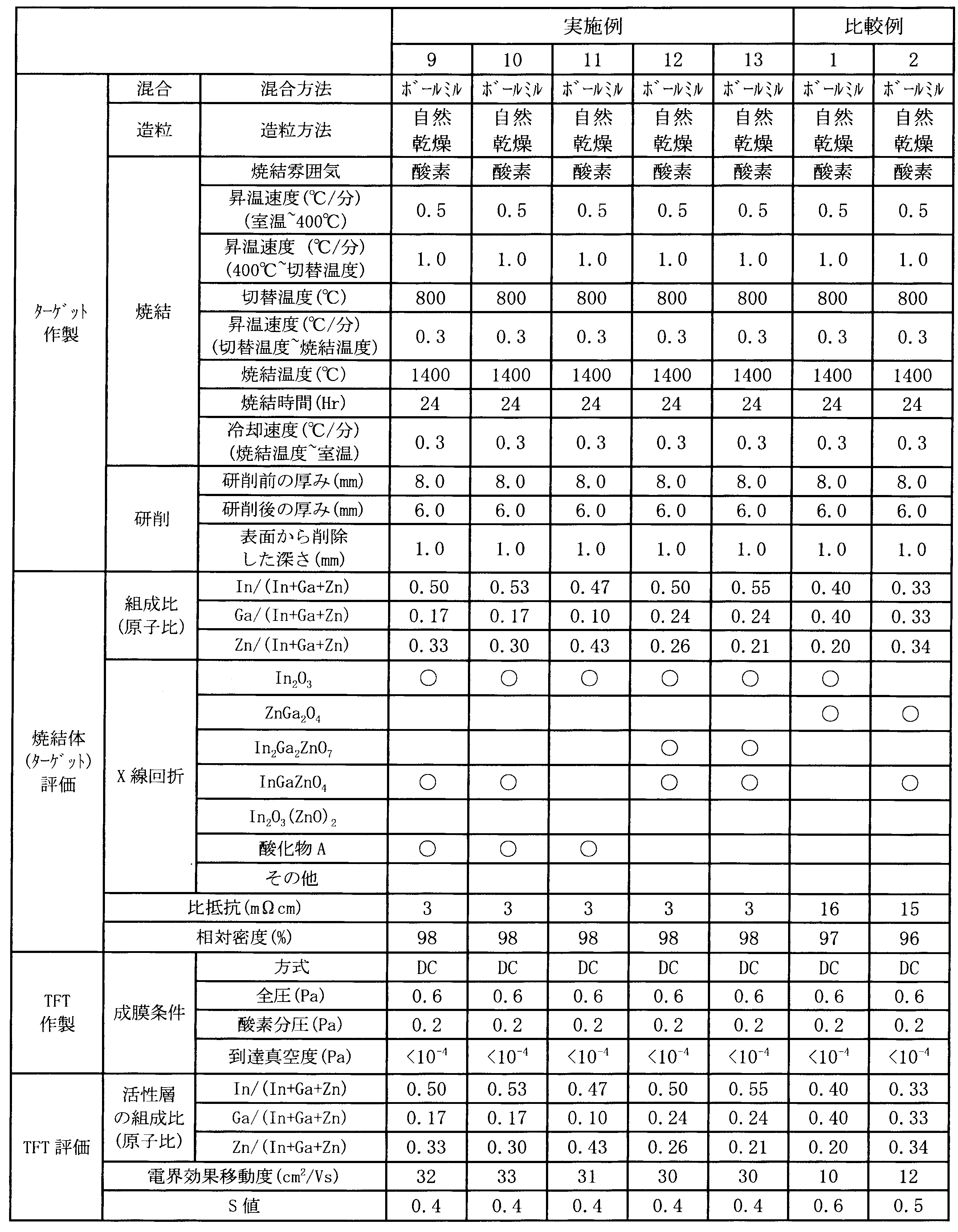
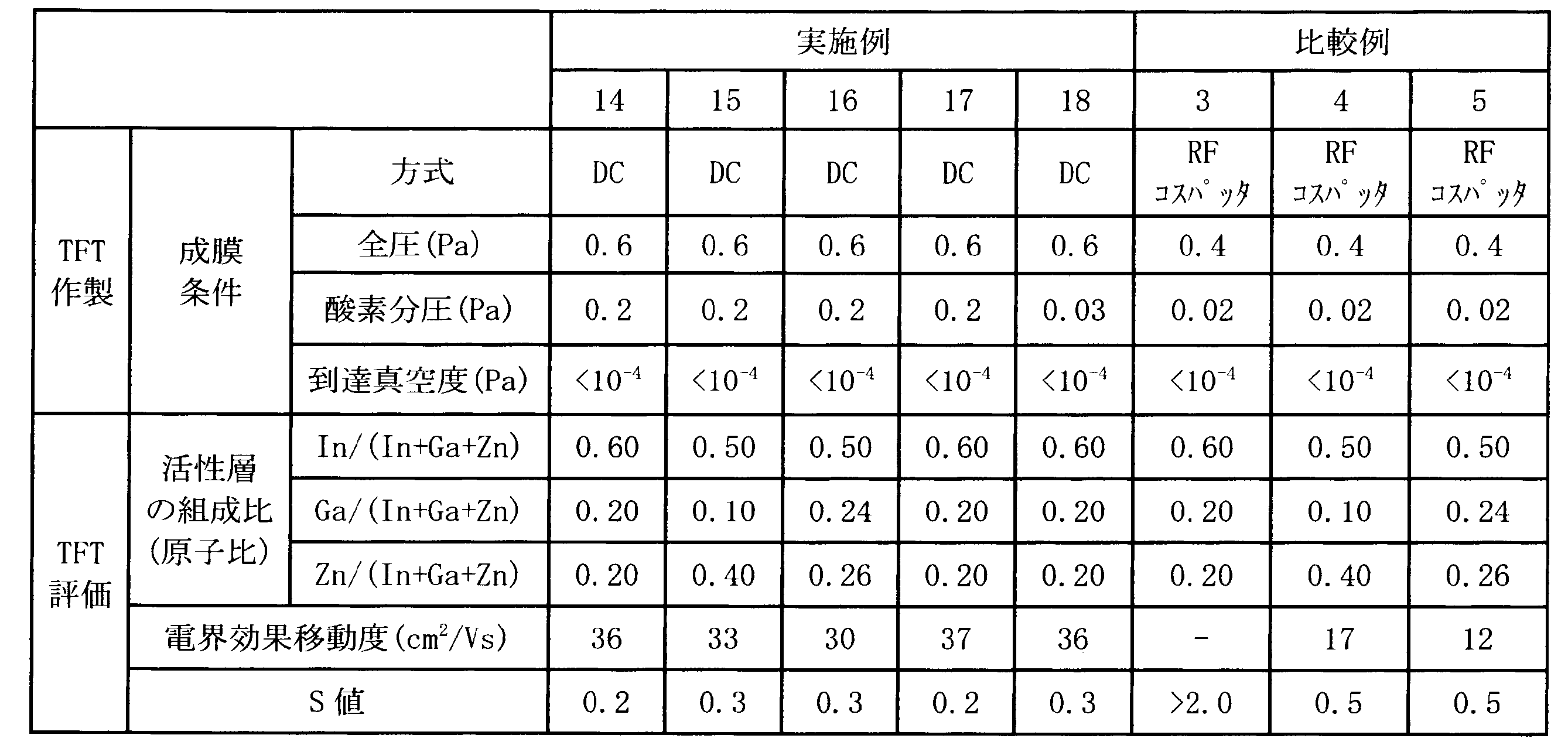
この明細書に記載の文献の内容を全てここに援用する。
Claims (9)
- 元素In,Ga及びZnを下記領域1、2又は3の原子比の範囲で含む酸化物を活性層とし、電界効果移動度が25cm2/Vs以上である薄膜トランジスタ。
領域1
0.58≦In/(In+Ga+Zn)≦0.68
0.15<Ga/(In+Ga+Zn)≦0.29
領域2
0.45≦In/(In+Ga+Zn)<0.58
0.09≦Ga/(In+Ga+Zn)<0.20
領域3
0.45≦In/(In+Ga+Zn)<0.58
0.20≦Ga/(In+Ga+Zn)≦0.27 - 電界効果移動度が30cm2/Vs以上である請求項1に記載の薄膜トランジスタ。
- 元素In,Ga及びZnを下記領域1、2又は3の原子比の範囲で含む酸化物焼結体からなるスパッタリングターゲット。
領域1
0.58≦In/(In+Ga+Zn)≦0.68
0.15<Ga/(In+Ga+Zn)≦0.29
領域2
0.45≦In/(In+Ga+Zn)<0.58
0.09≦Ga/(In+Ga+Zn)<0.20
領域3
0.45≦In/(In+Ga+Zn)<0.58
0.20≦Ga/(In+Ga+Zn)≦0.27 - 前記酸化物焼結体が、比抵抗15mΩcm未満、相対密度97%超である請求項3に記載のスパッタリングターゲット。
- 前記酸化物焼結体が、元素In,Ga及びZnを前記領域1の原子比の範囲で含み、(InGaO3)ZnOで表されるホモロガス構造化合物と、In2O3で表されるビックスバイト構造化合物とを含む、請求項3又は4に記載のスパッタリングターゲット。
- 前記酸化物焼結体が、元素In,Ga及びZnを前記領域2の原子比の範囲で含み、X線回折測定(Cukα線)により入射角(2θ)が、7.0°~8.4°、30.6°~32.0°、33.8°~35.8°、53.5°~56.5°及び56.5°~59.5°の各位置に回折ピークが観測される酸化物を含む、請求項3又は4に記載のスパッタリングターゲット。
- 前記酸化物焼結体が、元素In,Ga及びZnを前記領域3の原子比の範囲で含み、(InGaO3)ZnOで表されるホモロガス構造化合物を含む、請求項3又は4に記載のスパッタリングターゲット。
- 400℃~800℃の間を2.5℃/分以下で昇温する工程、
800℃~焼結温度の間を1.0℃/分以下で昇温する工程、及び
焼結温度1300~1450℃、焼結時間6~48時間で焼結する工程を含む請求項3~7のいずれかに記載のスパッタリングターゲットの製造方法。 - 請求項3~7のいずれかに記載のスパッタリングターゲットを用いて酸化物薄膜を作製する工程を含む請求項1又は2に記載の薄膜トランジスタの製造方法。
Priority Applications (4)
| Application Number | Priority Date | Filing Date | Title |
|---|---|---|---|
| KR1020137029565A KR101979468B1 (ko) | 2011-05-10 | 2012-05-01 | 박막 트랜지스터 |
| US14/116,328 US9054196B2 (en) | 2011-05-10 | 2012-05-01 | Sputtering target comprising an oxide sintered body comprising In, Ga, and Zn |
| CN201280022557.4A CN103518263B (zh) | 2011-05-10 | 2012-05-01 | 薄膜晶体管 |
| KR1020197013451A KR102048689B1 (ko) | 2011-05-10 | 2012-05-01 | 박막 트랜지스터 |
Applications Claiming Priority (2)
| Application Number | Priority Date | Filing Date | Title |
|---|---|---|---|
| JP2011105721A JP5767015B2 (ja) | 2011-05-10 | 2011-05-10 | 薄膜トランジスタ |
| JP2011-105721 | 2011-05-10 |
Publications (1)
| Publication Number | Publication Date |
|---|---|
| WO2012153494A1 true WO2012153494A1 (ja) | 2012-11-15 |
Family
ID=47138983
Family Applications (1)
| Application Number | Title | Priority Date | Filing Date |
|---|---|---|---|
| PCT/JP2012/002944 Ceased WO2012153494A1 (ja) | 2011-05-10 | 2012-05-01 | 薄膜トランジスタ |
Country Status (6)
| Country | Link |
|---|---|
| US (1) | US9054196B2 (ja) |
| JP (1) | JP5767015B2 (ja) |
| KR (2) | KR102048689B1 (ja) |
| CN (1) | CN103518263B (ja) |
| TW (1) | TWI543378B (ja) |
| WO (1) | WO2012153494A1 (ja) |
Cited By (3)
| Publication number | Priority date | Publication date | Assignee | Title |
|---|---|---|---|---|
| JPWO2013027391A1 (ja) * | 2011-08-22 | 2015-03-05 | 出光興産株式会社 | In−Ga−Sn系酸化物焼結体 |
| US9583633B2 (en) | 2013-03-08 | 2017-02-28 | Samsung Display Co., Ltd. | Oxide for semiconductor layer of thin film transistor, thin film transistor and display device |
| US10439068B2 (en) | 2015-02-12 | 2019-10-08 | Semiconductor Energy Laboratory Co., Ltd. | Oxide semiconductor film and semiconductor device |
Families Citing this family (9)
| Publication number | Priority date | Publication date | Assignee | Title |
|---|---|---|---|---|
| CN105308208A (zh) * | 2013-03-29 | 2016-02-03 | 吉坤日矿日石金属株式会社 | Igzo溅射靶和igzo膜 |
| KR101861459B1 (ko) * | 2014-03-14 | 2018-05-28 | 스미토모 긴조쿠 고잔 가부시키가이샤 | 산화물 소결체, 스퍼터링용 타겟 및 그것을 이용하여 얻어지는 산화물 반도체 박막 |
| FR3031834B1 (fr) * | 2015-01-21 | 2018-10-05 | Centre National De La Recherche Scientifique (Cnrs) | Fabrication d'un support semi-conducteur a base de nitrures d'elements iii |
| CN105543836B (zh) * | 2015-12-15 | 2017-11-21 | 西北工业大学 | 增材制造同轴送粉喷嘴汇聚特性测试装置 |
| JP6138307B2 (ja) * | 2016-03-09 | 2017-05-31 | Jx金属株式会社 | スパッタリングターゲット及びその製造方法 |
| CN110352263A (zh) * | 2018-02-08 | 2019-10-18 | 三菱综合材料株式会社 | 氧化物溅射靶及氧化物溅射靶的制造方法 |
| CN116240630A (zh) * | 2018-08-01 | 2023-06-09 | 出光兴产株式会社 | 晶体化合物、氧化物烧结体、溅射靶、晶质及无定形氧化物薄膜、薄膜晶体管及电子设备 |
| CN114958341A (zh) * | 2022-07-18 | 2022-08-30 | 合肥福纳科技有限公司 | 一种InP量子点及其制备方法 |
| TWI829578B (zh) * | 2023-04-14 | 2024-01-11 | 京元電子股份有限公司 | 晶圓儲放盒夾持扣具及其自動裝卸裝置 |
Citations (4)
| Publication number | Priority date | Publication date | Assignee | Title |
|---|---|---|---|---|
| JP2007212699A (ja) * | 2006-02-09 | 2007-08-23 | Idemitsu Kosan Co Ltd | 反射型tft基板及び反射型tft基板の製造方法 |
| WO2009075281A1 (ja) * | 2007-12-13 | 2009-06-18 | Idemitsu Kosan Co., Ltd. | 酸化物半導体を用いた電界効果型トランジスタ及びその製造方法 |
| WO2010140548A1 (ja) * | 2009-06-05 | 2010-12-09 | Jx日鉱日石金属株式会社 | 酸化物焼結体、その製造方法及び酸化物焼結体製造用原料粉末 |
| JP2011058011A (ja) * | 2009-09-07 | 2011-03-24 | Sumitomo Electric Ind Ltd | 導電性酸化物 |
Family Cites Families (8)
| Publication number | Priority date | Publication date | Assignee | Title |
|---|---|---|---|---|
| JP5006598B2 (ja) | 2005-09-16 | 2012-08-22 | キヤノン株式会社 | 電界効果型トランジスタ |
| JP4318689B2 (ja) | 2005-12-09 | 2009-08-26 | 出光興産株式会社 | n型無機半導体、n型無機半導体薄膜及びその製造方法 |
| EP2471972B1 (en) | 2006-12-13 | 2014-01-29 | Idemitsu Kosan Co., Ltd. | Sputtering target |
| KR100889688B1 (ko) | 2007-07-16 | 2009-03-19 | 삼성모바일디스플레이주식회사 | 반도체 활성층 제조 방법, 그를 이용한 박막 트랜지스터의제조 방법 및 반도체 활성층을 구비하는 박막 트랜지스터 |
| JP2009253204A (ja) * | 2008-04-10 | 2009-10-29 | Idemitsu Kosan Co Ltd | 酸化物半導体を用いた電界効果型トランジスタ及びその製造方法 |
| JP5403390B2 (ja) | 2008-05-16 | 2014-01-29 | 出光興産株式会社 | インジウム、ガリウム及び亜鉛を含む酸化物 |
| CN102105619B (zh) | 2008-06-06 | 2014-01-22 | 出光兴产株式会社 | 氧化物薄膜用溅射靶及其制造方法 |
| CN102245532A (zh) | 2008-12-15 | 2011-11-16 | 出光兴产株式会社 | 复合氧化物烧结体及由其构成的溅射靶 |
-
2011
- 2011-05-10 JP JP2011105721A patent/JP5767015B2/ja active Active
-
2012
- 2012-05-01 WO PCT/JP2012/002944 patent/WO2012153494A1/ja not_active Ceased
- 2012-05-01 US US14/116,328 patent/US9054196B2/en active Active
- 2012-05-01 KR KR1020197013451A patent/KR102048689B1/ko active Active
- 2012-05-01 CN CN201280022557.4A patent/CN103518263B/zh active Active
- 2012-05-01 KR KR1020137029565A patent/KR101979468B1/ko active Active
- 2012-05-10 TW TW101116732A patent/TWI543378B/zh active
Patent Citations (4)
| Publication number | Priority date | Publication date | Assignee | Title |
|---|---|---|---|---|
| JP2007212699A (ja) * | 2006-02-09 | 2007-08-23 | Idemitsu Kosan Co Ltd | 反射型tft基板及び反射型tft基板の製造方法 |
| WO2009075281A1 (ja) * | 2007-12-13 | 2009-06-18 | Idemitsu Kosan Co., Ltd. | 酸化物半導体を用いた電界効果型トランジスタ及びその製造方法 |
| WO2010140548A1 (ja) * | 2009-06-05 | 2010-12-09 | Jx日鉱日石金属株式会社 | 酸化物焼結体、その製造方法及び酸化物焼結体製造用原料粉末 |
| JP2011058011A (ja) * | 2009-09-07 | 2011-03-24 | Sumitomo Electric Ind Ltd | 導電性酸化物 |
Cited By (5)
| Publication number | Priority date | Publication date | Assignee | Title |
|---|---|---|---|---|
| JPWO2013027391A1 (ja) * | 2011-08-22 | 2015-03-05 | 出光興産株式会社 | In−Ga−Sn系酸化物焼結体 |
| US9583633B2 (en) | 2013-03-08 | 2017-02-28 | Samsung Display Co., Ltd. | Oxide for semiconductor layer of thin film transistor, thin film transistor and display device |
| US10439068B2 (en) | 2015-02-12 | 2019-10-08 | Semiconductor Energy Laboratory Co., Ltd. | Oxide semiconductor film and semiconductor device |
| US11380799B2 (en) | 2015-02-12 | 2022-07-05 | Semiconductor Energy Laboratory Co., Ltd. | Oxide semiconductor film and semiconductor device |
| US11532755B2 (en) | 2015-02-12 | 2022-12-20 | Semiconductor Energy Laboratory Co., Ltd. | Oxide semiconductor film and semiconductor device |
Also Published As
| Publication number | Publication date |
|---|---|
| US20140084289A1 (en) | 2014-03-27 |
| TW201301524A (zh) | 2013-01-01 |
| CN103518263A (zh) | 2014-01-15 |
| CN103518263B (zh) | 2017-06-23 |
| KR101979468B1 (ko) | 2019-05-16 |
| TWI543378B (zh) | 2016-07-21 |
| JP5767015B2 (ja) | 2015-08-19 |
| JP2012238678A (ja) | 2012-12-06 |
| US9054196B2 (en) | 2015-06-09 |
| KR20190053299A (ko) | 2019-05-17 |
| KR20140022874A (ko) | 2014-02-25 |
| KR102048689B1 (ko) | 2019-11-26 |
Similar Documents
| Publication | Publication Date | Title |
|---|---|---|
| JP5767015B2 (ja) | 薄膜トランジスタ | |
| JP6314198B2 (ja) | 複合酸化物焼結体及びそれからなるスパッタリングターゲット | |
| JP5928856B2 (ja) | InGaO3(ZnO)結晶相からなる酸化物半導体用スパッタリングターゲット及びその製造方法 | |
| US9767998B2 (en) | Sputtering target | |
| JP5145513B2 (ja) | 複合酸化物焼結体及びそれからなるスパッタリングターゲット | |
| JP5690063B2 (ja) | In−Ga−Zn系酸化物焼結体スパッタリングターゲット及び薄膜トランジスタ | |
| CN102770577B (zh) | In-Ga-Sn系氧化物烧结体、靶、氧化物半导体膜、及半导体元件 | |
| JP5596963B2 (ja) | スパッタリングターゲット及びそれを用いた薄膜トランジスタ | |
| JP5096250B2 (ja) | 酸化物焼結体の製造方法、酸化物焼結体、スパッタリングタ−ゲット、酸化物薄膜、薄膜トランジスタの製造方法及び半導体装置 | |
| US20120118726A1 (en) | In-ga-zn-o type sputtering target | |
| TWI636959B (zh) | Sputtering target, oxide semiconductor film, and the like | |
| JPWO2009157535A6 (ja) | InGaO3(ZnO)結晶相からなる酸化物半導体用スパッタリングターゲット及びその製造方法 | |
| WO2011061930A1 (ja) | In-Ga-Zn系酸化物、酸化物焼結体、及びスパッタリングターゲット | |
| US11443943B2 (en) | Sputtering target, oxide semiconductor thin film, and method for producing these | |
| JP2012056842A (ja) | In−Ga−Zn系酸化物、酸化物焼結体、及びスパッタリングターゲット |
Legal Events
| Date | Code | Title | Description |
|---|---|---|---|
| 121 | Ep: the epo has been informed by wipo that ep was designated in this application |
Ref document number: 12781749 Country of ref document: EP Kind code of ref document: A1 |
|
| ENP | Entry into the national phase |
Ref document number: 20137029565 Country of ref document: KR Kind code of ref document: A |
|
| NENP | Non-entry into the national phase |
Ref country code: DE |
|
| WWE | Wipo information: entry into national phase |
Ref document number: 14116328 Country of ref document: US |
|
| 122 | Ep: pct application non-entry in european phase |
Ref document number: 12781749 Country of ref document: EP Kind code of ref document: A1 |