WO2012144364A1 - コネクタ - Google Patents
コネクタ Download PDFInfo
- Publication number
- WO2012144364A1 WO2012144364A1 PCT/JP2012/059659 JP2012059659W WO2012144364A1 WO 2012144364 A1 WO2012144364 A1 WO 2012144364A1 JP 2012059659 W JP2012059659 W JP 2012059659W WO 2012144364 A1 WO2012144364 A1 WO 2012144364A1
- Authority
- WO
- WIPO (PCT)
- Prior art keywords
- connector
- cavity
- cavities
- holder
- main body
- Prior art date
Links
Images


Classifications
-
- H—ELECTRICITY
- H01—ELECTRIC ELEMENTS
- H01R—ELECTRICALLY-CONDUCTIVE CONNECTIONS; STRUCTURAL ASSOCIATIONS OF A PLURALITY OF MUTUALLY-INSULATED ELECTRICAL CONNECTING ELEMENTS; COUPLING DEVICES; CURRENT COLLECTORS
- H01R13/00—Details of coupling devices of the kinds covered by groups H01R12/70 or H01R24/00 - H01R33/00
- H01R13/46—Bases; Cases
- H01R13/514—Bases; Cases composed as a modular blocks or assembly, i.e. composed of co-operating parts provided with contact members or holding contact members between them
-
- H—ELECTRICITY
- H01—ELECTRIC ELEMENTS
- H01R—ELECTRICALLY-CONDUCTIVE CONNECTIONS; STRUCTURAL ASSOCIATIONS OF A PLURALITY OF MUTUALLY-INSULATED ELECTRICAL CONNECTING ELEMENTS; COUPLING DEVICES; CURRENT COLLECTORS
- H01R13/00—Details of coupling devices of the kinds covered by groups H01R12/70 or H01R24/00 - H01R33/00
- H01R13/46—Bases; Cases
- H01R13/516—Means for holding or embracing insulating body, e.g. casing, hoods
- H01R13/518—Means for holding or embracing insulating body, e.g. casing, hoods for holding or embracing several coupling parts, e.g. frames
-
- H—ELECTRICITY
- H01—ELECTRIC ELEMENTS
- H01R—ELECTRICALLY-CONDUCTIVE CONNECTIONS; STRUCTURAL ASSOCIATIONS OF A PLURALITY OF MUTUALLY-INSULATED ELECTRICAL CONNECTING ELEMENTS; COUPLING DEVICES; CURRENT COLLECTORS
- H01R13/00—Details of coupling devices of the kinds covered by groups H01R12/70 or H01R24/00 - H01R33/00
- H01R13/62—Means for facilitating engagement or disengagement of coupling parts or for holding them in engagement
- H01R13/629—Additional means for facilitating engagement or disengagement of coupling parts, e.g. aligning or guiding means, levers, gas pressure electrical locking indicators, manufacturing tolerances
-
- H—ELECTRICITY
- H01—ELECTRIC ELEMENTS
- H01R—ELECTRICALLY-CONDUCTIVE CONNECTIONS; STRUCTURAL ASSOCIATIONS OF A PLURALITY OF MUTUALLY-INSULATED ELECTRICAL CONNECTING ELEMENTS; COUPLING DEVICES; CURRENT COLLECTORS
- H01R13/00—Details of coupling devices of the kinds covered by groups H01R12/70 or H01R24/00 - H01R33/00
- H01R13/62—Means for facilitating engagement or disengagement of coupling parts or for holding them in engagement
- H01R13/627—Snap or like fastening
- H01R13/6271—Latching means integral with the housing
- H01R13/6272—Latching means integral with the housing comprising a single latching arm
Definitions
- the present invention relates to a connector having a plurality of cavities in which terminal fittings connected to electric wire terminals are accommodated, and more particularly, a connector suitable as a connector to be connected to a plurality of mating connectors provided in each of stacked members. About.
- the electrical / electronic device (member) is provided with a connector for electrical connection to a power source and other electrical / electronic device (member).
- a connector for electrical connection to a power source and other electrical / electronic device (member).
- bus bars and tab terminals are provided on a wiring board in an electrical junction box, and these bus bars and tab terminals are accommodated in a connector housing formed integrally with a main cover that covers the wiring board. The resulting connector is provided in the electrical junction box.
- these may be stacked or arranged in parallel.
- the member is a flat plate, such as a substrate, it may be laminated.
- these connectors have the same configuration, so that each connector is stacked and arranged at the same position on the same side of the member. .
- the connectors on the laminated member side are laminated and arranged at predetermined intervals designed in advance.
- a tolerance due to the lamination often occurs in the interval between the connectors on the laminated member side.
- the problem to be solved by the present invention is that, even when a tolerance due to lamination occurs on the laminated electrical / electronic equipment (member) side, the mating connectors of each of these equipment (members) are collectively connected to the connector. It is to provide a connector that can be connected.
- a connector according to the present invention is a connector having a plurality of cavities in which terminal fittings connected to electric wire terminals are accommodated, and the cavities are configured in a cylindrical shape as separate members independent of the connector body.
- the plurality of cavities are also configured as separate members independent of each other, and the connector body serves as a holder for housing the plurality of cavities, and the plurality of cavities are individually locked to the connector body, In this locking portion, clearances are provided between individual cavities and the connector body, and the gist is that movement of the cavities with respect to the connector body is allowed by this clearance. is there.
- the connector body has a plurality of locking holes for inserting and locking the cavity, and a cover for preventing the inserted cavity from dropping from the connector body at a position behind the inserted cavity. It is preferable to provide.
- a clearance is provided between the inserted cavity and the cover to allow movement of the inserted cavity with respect to the connector body.
- examples of the reference cavity include a cavity whose movement is restricted with respect to the connector body by being integrally formed with the connector body.
- examples of the reference cavity include a cavity whose movement is restricted with respect to the connector body by being press-fitted into the connector body.
- examples of the reference cavity include those in which movement is restricted with respect to the connector body by being integrally formed with the cover.
- examples of the reference cavity include those whose movement is restricted with respect to the connector body by being pressed by the cover.
- the cover is formed with a through hole through which an electric wire connected to the terminal fitting accommodated in the cavity is passed, and the guide for determining the wiring direction of the electric wire from the through hole is formed in the through hole. It is preferable that the grooves are continuous.
- the connector according to the present invention is provided in each of the laminated members and collectively connects the plurality of connectors in the laminated state.
- the individual cavities are allowed to move relative to the connector main body by the clearance at the engaging portion between the individual cavities independent of the connector main body and the connector main body. For this reason, when the mating connectors of the stacked electrical / electronic devices (members) are collectively connected to each other, the mating connectors stacked on the stacked electrical / electronic devices (members) side With respect to the stacking tolerances that occur during this time, the individual cavities can be moved to align with the respective mating connector to which the individual cavities are fitted to absorb the stacking tolerances. Accordingly, the stacked mating connectors can be collectively connected to each other.
- the connector body has a plurality of locking holes for inserting and locking the cavity
- a cover is provided at a position behind the inserted cavity to prevent the inserted cavity from falling off the connector body. Can securely lock the cavity in the connector body.
- the cavity is allowed to move even when the cover is provided. Can be maintained.
- the connector when there is a reference cavity whose movement is restricted with respect to the connector main body, the connector can be easily fitted to the mating connector with reference to the reference cavity.
- the cover is formed with a through hole through which an electric wire connected to the terminal fitting accommodated in the cavity is passed, and a guide groove for determining the wiring direction of the electric wire is connected to the through hole from the through hole. If there is, it is possible to regulate the direction of wiring.
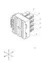
- FIG. 1 is an external perspective view of a connector according to an embodiment of the present invention. It is an external appearance perspective view of the cavity of a connector. It is a left view of the cavity of a connector. It is a front view of the cavity of a connector. It is an external appearance perspective view of the holder (connector main body) of a connector. It is an external appearance perspective view showing the holder made into the state which can see the inside. It is a rear view of the holder of a connector. It is a front view of the holder of a connector. It is a left view of the holder of a connector. It is a schematic diagram which shows the state which inserted the cavity in the one part insertion hole of the holder.
- FIG. 12 is a cross-sectional view of the connector of FIG. 11 along the line AA.
- FIG. 12 is a cross-sectional view of the connector of FIG. 11 along the line BB.
- FIG. 1 is an external perspective view of a connector according to an embodiment of the present invention.
- the front, rear, up, down, left and right directions are specified.
- the side mated with the mating connector is the front side.
- a connector 10 includes a plurality of cavities 12 in which terminal fittings connected to electric wire terminals are accommodated, and a connector main body 14.
- the plurality of cavities 12 are configured in a cylindrical shape as separate members independent of the connector main body 14.
- the plurality of cavities 12 are also configured as separate members independent of each other.
- the connector body 14 is a holder that accommodates the plurality of cavities 12 (hereinafter, the connector body 14 may be expressed as the holder 14).
- FIG. 1 is a left side view of the holder 14.
- FIG. 3 is a left side view of the cavity 12
- FIG. 4 is a front view of the cavity 12.
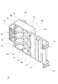
- 5 to 9 are drawings showing the holder 14 (connector body 14).
- 5 is an external perspective view of the holder 14
- FIG. 6 is an external perspective view showing the holder 14 in a state where the inside can be seen
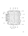
- FIG. 7 is a rear view of the holder 14
- FIG. 8 is a front view of the holder 14.
- FIG. 9 is a left side view of the holder 14.
- the cavity 12 is formed in a rectangular tube shape so that a terminal fitting (not shown) can be accommodated therein.
- the terminal fitting is locked inside the cavity 12 by being locked to a locking projection (not shown) inside the cavity 12.
- the opening side 12a behind the cavity 12 is a side into which a terminal fitting (cylindrical terminal 70 described later) is inserted, and the opening side 12b before the cavity 12 is a terminal fitting (pin terminal 62) of a mating connector 60 described later. Is the side to be inserted.
- Both the rear opening side 12a and the front opening side 12b of the cavity 12 are formed with a taper that widens the entrance so that a terminal fitting (a cylindrical terminal 70 and a pin terminal 62 described later) can be easily inserted.
- a pair of protrusions 22a and 22b extending the entire length of the cavity 12 in the front-rear direction is formed on one side of the cavity 12 (right side in FIG. 2). Further, on the other side of the cavity 12 (left side in FIG. 2), a pair of protrusions 24 a and 24 b extending only to a part of the rear side of the cavity 12 are formed.
- the groove between the pair of protrusions 22a and 22b on one side and the groove between the pair of protrusions 24a and 24b on the other side serves as a guide, so that the cavity 12 can be easily inserted into the holder 14.
- a lance locking hole 26 is formed as a recessed portion that is depressed by one step, and a lance 44 of the holder 14 described later enters and the lance 44 is engaged. It has come to be stopped.
- a protrusion-like stopper 28 that protrudes further in the right direction is formed at the rear end of the upper protrusion 22a of the pair of protrusions 22a, 22b on one side. 38.
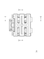
- the holder 14 includes a box-shaped holder main body 30 surrounded by a front surface 30a, both side surfaces 30b and 30c, and upper and lower surfaces 30d and 30e, and an open rear side 30f.
- a cover 32 that covers the rear side 30f that is opened, and a lock 34 that is engaged with the mating connector when the holder 14 is fitted to the mating connector.
- the inside of the holder body 30 is a storage chamber that stores a portion of the cavity 12 that is not fitted to the mating connector.
- the front surface 30 a of the holder body 30 has a plurality of insertion holes 36 into which the individual cavities 12 are inserted so that a portion of the cavity 12 to be received that fits into the mating connector protrudes from the holder body 30. Is formed through. In the configuration shown in FIGS. 5 to 9, two insertion holes 36 are arranged in the left-right direction, and four insertion holes 36 are arranged in the up-down direction.
- an abutting protrusion 38 on which the stopper 28 of the cavity 12 abuts projects inside the front surface 30 a of the holder body 30, and It is formed so as to be continuous along the vertical direction.
- the contact protrusions 38 also serve as ribs that reinforce the front surface 30a of the holder main body 30, and are connected to the upper and lower ribs 40 and 42 that reinforce the upper and lower surfaces 30d and 30e of the holder main body 30 in the same manner. .
- lances 44 Inside the both side surfaces 30b and 30c of the holder body 30, there are provided lances 44 that enter and are locked into the lance locking holes 26 of the cavity 12 when the cavity 12 is inserted.
- an engaging claw 46 that engages with an engaging piece 50 of the cover 32 described later is provided.
- the cover 32 is connected to the right rear end of the holder body 30 by two hinges 48 provided at the right end.
- the cover 32 can be rotated with the hinge 48 as a rotation center, and the opening of the rear side 30f of the holder body 30 can be opened and closed by the rotation of the cover 32.
- Engaging pieces 50 that engage with engaging claws 46 formed on the outer side of the left side surface 30 b of the holder body 30 are provided at two positions above and below the left end of the cover 32.
- a protrusion 52 extending in the vertical direction is formed at the central portion of the inner surface of the cover 32.
- the cover 32 covers the rear side 30f of the holder body 30, it is inserted into the insertion hole 36 of the holder 14. It faces the rear end face of the protruding stopper 28 formed at the rear end of the cavity 12 at a predetermined interval (clearance).
- a through hole 54 through which an electric wire connected to a terminal fitting accommodated in the cavity 12 passes is formed on both sides of the portion where the protrusion 52 is formed.
- the through hole 54 faces the opening side 12 a behind the cavity 12, and the terminal fitting to which the wire terminal is connected is accommodated in the cavity 12 through the through hole 54.
- the electric wire connected to the terminal fitting housed inside the cavity 12 is drawn out of the connector 10 through the through hole 54.
- a guide groove 56 extending in the upward direction or the downward direction is connected to the through hole 54, and the guide direction of the electric wire from the through hole 54 is restricted upward or downward by the guide groove 56. Can do.
- the lock 34 is formed integrally with the holder body 30 on the outside of the left side surface 30b of the holder body 30 so that the fitting state can be maintained when the connector 10 is fitted with the mating connector.
- FIG. 10 shows a state in which the cavity 12 is inserted into a part of the insertion hole 36 of the holder 14 having such a configuration.
- the cavity 12 to be inserted into the left insertion hole 36 has a pair of protrusions 22a and 22b on one side arranged on the right side and a pair of protrusions 24a and 24b on the other side arranged on the left side.
- a pair of protrusions 22a and 22b on one side are arranged on the left side
- a pair of protrusions 24a and 24b on the other side are arranged on the right side.
- the protruding stopper 28 of the cavity 12 inserted into the left insertion hole 36 is disposed on the upper side, and the protruding stopper 28 of the cavity 12 inserted into the right insertion hole 36 is disposed on the lower side. . Since these stoppers 28 are arranged in pairs so as to overlap in the vertical direction, the size of the connector 10 in the left-right direction can be reduced.
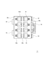
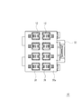
- 11 to 14 are views showing the connector 10 as a completed form in which the cavity 12 is inserted into the insertion hole 36 of the holder 14.
- 11 is a rear view of the connector 10
- FIG. 12 is a cross-sectional view taken along the line AA of the connector 10 in FIG. 11
- FIG. 13 is a cross-sectional view taken along the line BB of the connector 10 in FIG. 2 is a front view of the connector 10.
- FIG. 12 is a cross-sectional view taken along the line AA of the connector 10 in FIG. 11
- the cavity 12 inserted into the insertion hole 36 of the holder 14 is locked to the holder 14 by the lance 44 of the holder 14 entering the lance locking hole 26 of the cavity 12.
- the pair of protrusions 24 a and 24 b on the other side having the lance locking holes 26 of the cavity 12 are brought into contact with the front surface 30 a of the holder body 30, and the stopper 28 of the cavity 12 is brought into contact with the holder 14. It abuts on the strip 38.
- a clearance L is provided between the side surface 12 c having the lance locking hole 26 of the cavity 12 and the insertion hole 36 of the holder 14.
- a clearance L is provided between the pair of protrusions 22 a, 22 b on one side having the stopper 28 of the cavity 12 and the protrusion protrusion 38 for the holder 14.
- a clearance L is provided between the stopper 28 of the cavity 12 and the protrusion 52 on the inner surface of the cover 32.
- FIG. 15 is a schematic diagram showing a state before the connector 10 and the mating connector 62 are fitted together.
- FIG. 16 is a schematic view showing a state in which the connector 10 and the mating connector 62 are fitted and cut along the front-rear direction at the center position of the cavity 12.
- the electrical / electronic device (member) 60 such as a substrate that is collectively connected by the connector 10 of the present invention includes a mating connector 62 at one edge.
- the mating connector 62 includes a pin terminal 64 drawn from one end edge and a hood portion 66 that covers the pin terminal 64.
- two pin terminals 64 are drawn from one end edge.
- the two hood portions 66 that individually cover the two pin terminals 64 are connected to each other by integral molding.
- the hood portion 66 is formed in a rectangular tube shape in cross section, is open at the front side to which the connector 10 of the present invention is fitted, and has a length covering the periphery of the pin terminal 64.
- the electric / electronic devices (members) 60 having such a configuration gather, and the plurality of electric / electronic devices (members) 60 are stacked in the vertical direction.
- the mating connectors 62 of the plurality of electric / electronic devices (members) 60 are arranged in a vertical direction and are grouped together by arranging the plurality of electric / electronic devices (members) 60 in a stacked manner.
- the left side of the two hood portions 66 of the electric / electronic device (member) 60 located at the lowermost layer is directed upward to the left side of the two hood portions 66 of the electric / electronic device (member) 60 located at the uppermost layer.
- a plate-shaped guide member 68 extending in the direction is provided, and the left side of the two hood portions 66 of each electric / electronic device (member) 60 is in contact with the guide member 68 and positioned.
- the mating connectors 62 of the plurality of electric / electronic devices (members) 60 are arranged in the vertical direction and grouped together.
- a lock locking claw (not shown) that locks the lock 34 of the connector 10 is provided on the left outer surface of the guide member 68.
- all the cavities 12 of the plurality of cavities 12 are allowed to move with respect to the holder 14, but one or more of the plurality of cavities 12 It is also possible to adopt a configuration in which the movement of the cavity is restricted with respect to the holder. Since the movement of such a cavity is restricted with respect to the holder, it can be used as a reference cavity for positioning when the connector of the present invention is fitted to the mating connector. As a result, the connector can be easily fitted into the mating connector.
- the form in which the movement of the cavity is restricted, 1) the form in which the cavity is integrally formed with the holder, 2) the form in which the cavity is press-fitted into the insertion hole of the holder body, and 3) the cavity is integrally formed with the cover. 2) a form in which the cavity is pressed against the cover, and the like.
- a cavity shaped like this can be used as a reference cavity.
- the cavities 12 are arranged in two rows in the left-right direction.
- the cavities 12 may be arranged in one row in the left-right direction, or three or more rows are arranged in parallel. It may be a configuration.
- the cover 32 is provided, the structure in which the cover 32 is not provided may be sufficient.
- the cavity 12 is a rectangular tube shape, other forms, such as a cylindrical shape, may be sufficient.
- the guide groove 56 formed in the cover 32 penetrates both surfaces of the cover 32 as in the case of the through hole 54, but does not penetrate both surfaces of the cover 32, and the outer surface of the cover 32. It can also be formed like a recessed portion with a recess.
Abstract
積層された電気・電子機器(部材)側に積層による公差が生じる場合にも、これらの機器(部材)が各々備える相手側コネクタをまとめて一括してコネクタ接続できるコネクタを提供する。 端子金具が収容されるキャビティ(12)を複数有し、キャビティ(12)がコネクタ本体(14)から独立する別部材として筒状に構成されるとともに、これら複数のキャビティ(12)同士も互いに独立する別部材として構成され、コネクタ本体(14)がこれら複数のキャビティ(12)を収容するホルダとなってこれら複数のキャビティ(12)は個別にコネクタ本体(14)に係止されており、この係止部分において、個々のキャビティ(12)とコネクタ本体(14)との間にはクリアランスが設けられており、このクリアランスによりキャビティ(12)はコネクタ本体(14)に対して動きが許容されている。
Description
本発明は、電線端末に接続される端子金具が収容されるキャビティを複数有するコネクタに関し、さらに詳しくは、積層された部材の各々に備えられた複数の相手側コネクタに接続するコネクタとして好適なコネクタに関する。
電気・電子機器(部材)には、電源や他の電気・電子機器(部材)に電気接続するためのコネクタが設けられている。例えば特許文献1には、電気接続箱内の配線板にバスバーやタブ端子が設けられており、この配線板を覆うメインカバーに一体に形成されたコネクタハウジング内にこれらのバスバーやタブ端子が収容されてなるコネクタが電気接続箱に設けられている。
例えば同じような構成の電気・電子機器(部材)を複数用いる場合などにおいては、これらを積層配置したり並列配置したりすることがある。例えば基板など、その部材が平板状である場合には、特に積層配置することがある。同じような構成の複数の電気・電子機器(部材)を積層して用いる場合には、これらは同じような構成であることから、各々のコネクタは部材の同じ側の同じ位置に積層配置される。
このとき、設計では、積層された部材側のコネクタ同士は、予め設計された所定の間隔で積層配置される。しかしながら、実際には、各部材の設計公差などにより、積層された部材側のコネクタ同士の間隔には、積層による公差が生じることが多い。
このため、これらのコネクタをまとめて一括してコネクタ接続する場合には、積層された部材側に生じる積層公差を考慮してコネクタ接続を行わなければならない。このとき、積層された部材側で公差を矯正するのは非常に困難で、可能であったとしても大幅なコスト増につながるおそれがある。そのため、従来のコネクタでは、これらのコネクタをまとめて一括してコネクタ接続することができなかった。
本発明が解決しようとする課題は、積層された電気・電子機器(部材)側に積層による公差が生じる場合にも、これらの機器(部材)が各々備える相手側コネクタをまとめて一括してコネクタ接続できるコネクタを提供することにある。
上記課題を解決するため本発明に係るコネクタは、電線端末に接続される端子金具が収容されるキャビティを複数有するコネクタであって、前記キャビティがコネクタ本体から独立する別部材として筒状に構成されるとともに、これら複数のキャビティ同士も互いに独立する別部材として構成され、前記コネクタ本体がこれら複数のキャビティを収容するホルダとなってこれら複数のキャビティは個別に前記コネクタ本体に係止されており、この係止部分において、個々のキャビティと前記コネクタ本体との間にはクリアランスが設けられており、このクリアランスにより前記キャビティは前記コネクタ本体に対して動きが許容されていることを要旨とするものである。
この際、前記コネクタ本体は、前記キャビティを挿入して係止する係止孔を複数有するとともに、挿入したキャビティの後ろとなる位置に、挿入したキャビティが前記コネクタ本体から脱落するのを抑えるカバーを備えることが好ましい。
このとき、前記挿入したキャビティと前記カバーとの間には、前記コネクタ本体に対する前記挿入したキャビティの動きが許容されるクリアランスが設けられていることが好ましい。
そして、本発明に係るコネクタにおいては、前記コネクタ本体に対して動きが規制されている基準のキャビティが存在することが望ましい。
ここで、基準のキャビティとしては、前記コネクタ本体に一体成形されることにより、前記コネクタ本体に対して動きが規制されているものを挙げることができる。
また、基準のキャビティとしては、前記コネクタ本体に圧入されることにより、前記コネクタ本体に対して動きが規制されているものを挙げることができる。
また、基準のキャビティとしては、前記カバーに一体成形されることにより、前記コネクタ本体に対して動きが規制されているものを挙げることができる。
また、基準のキャビティとしては、前記カバーに押圧されることにより、前記コネクタ本体に対して動きが規制されているものを挙げることができる。
そして、前記カバーには、前記キャビティに収容される端子金具と接続される電線が通される貫通孔が形成されており、この貫通孔には、この貫通孔から電線の配策方向を決めるガイド溝が連なっていることが好ましい。
そして、本発明に係るコネクタは、積層された部材の各々に備えられ、積層された状態にある複数のコネクタをまとめて一括して接続するものであることが好ましい。
本発明に係るコネクタによれば、コネクタ本体から独立する個々のキャビティとコネクタ本体との係止部分におけるクリアランスによって個々のキャビティがコネクタ本体に対して動きが許容される。このため、積層された電気・電子機器(部材)が各々備える相手側コネクタをまとめて一括してコネクタ接続するときに、積層された電気・電子機器(部材)側で積層された相手側コネクタ同士の間に生じる積層公差に対して、個々のキャビティを動かすことにより個々のキャビティが嵌合される個々の相手側コネクタに位置合わせをしてその積層公差を吸収することができる。これにより、積層された相手側コネクタをまとめて一括してコネクタ接続することができる。
この際、コネクタ本体が、キャビティを挿入して係止する係止孔を複数有するとともに、挿入したキャビティの後ろとなる位置に、挿入したキャビティがコネクタ本体から脱落するのを抑えるカバーを備える場合には、確実に、コネクタ本体にキャビティを係止させることができる。
このとき、挿入したキャビティとカバーとの間に、コネクタ本体に対する挿入したキャビティの動きが許容されるクリアランスが設けられている場合には、カバーを設ける構成にしたときにも、キャビティの動きが許容される状態を維持することができる。
そして、本発明に係るコネクタにおいて、コネクタ本体に対して動きが規制されている基準のキャビティが存在する場合には、基準のキャビティを基準にして相手側コネクタと嵌合しやすくなる。
そして、カバーに、キャビティに収容される端子金具と接続される電線が通される貫通孔が形成されており、この貫通孔に、この貫通孔から電線の配策方向を決めるガイド溝が連なっている場合には、電線の配策方向を規制することができる。
以下、本発明の一実施形態について図面を参照して詳細に説明する。図1は、本発明の一実施形態に係るコネクタの外観斜視図である。なお、各図においては、便宜上、図1に示すように、コネクタの前後上下左右の方向を特定する。相手側コネクタと嵌合される側を前側としている。
図1に示すように、本発明の一実施形態に係るコネクタ10は、電線端末に接続される端子金具が収容される複数のキャビティ12と、コネクタ本体14とを備えている。複数のキャビティ12は、コネクタ本体14から独立する別部材として筒状に構成されている。また、複数のキャビティ12同士も、互いに独立する別部材として構成されている。コネクタ本体14は、これら複数のキャビティ12を収容するホルダとなっている(以下、コネクタ本体14をホルダ14として表現することがある。)。
図2~4は、コネクタ10のキャビティ12を表す図面である。図2はキャビティ12の外観斜視図であり、図3はキャビティ12の左側面図であり、図4はキャビティ12の前面図である。図5~9は、ホルダ14(コネクタ本体14)を表す図面である。図5はホルダ14の外観斜視図であり、図6は内部が見える状態にされたホルダ14を表す外観斜視図であり、図7はホルダ14の後面図であり、図8はホルダ14の前面図であり、図9はホルダ14の左側面図である。
図2~4に示すように、キャビティ12は、角筒状に構成されてその内部に図示しない端子金具が収容できるようになっている。端子金具は、キャビティ12の内部の図示しない係止突起に係止されることによりキャビティ12の内部に係止される。キャビティ12の後ろの開口側12aは端子金具(後述する筒型端子70)が挿入される側であり、キャビティ12の前の開口側12bは後述する相手側コネクタ60の端子金具(ピン端子62)が挿入される側である。キャビティ12の後ろの開口側12aおよび前の開口側12bのいずれも、端子金具(後述する筒型端子70およびピン端子62)が挿入されやすいように入口を広げるテーパが形成されている。
キャビティ12の一方側(図2の右側)には、キャビティ12の前後方向の全長に延びる一対の突条22a,22bが形成されている。また、キャビティ12の他方側(図2の左側)には、キャビティ12の後側の一部分にのみ延びる一対の突条24a,24bが形成されている。一方側の一対の突条22a,22b間の溝と他方側の一対の突条24a,24b間の溝がガイドとなって、ホルダ14にキャビティ12を挿入しやすくなっている。
他方側の一対の突条24a,24b間の溝の中央部分には、一段窪んだ凹部となるランス係止孔26が形成されており、後述するホルダ14のランス44が入り込んでランス44が係止されるようになっている。
一方側の一対の突条22a,22bのうち上側の突条22aの後端には、右方向にさらに突出する突状のストッパ28が形成されており、後述するホルダ14の当接用突条38に当接されるようになっている。
図5~9に示すように、ホルダ14は、前面30aと両側面30b,30cと上下面30d,30eとで囲まれるとともに後側30fが開口された箱状のホルダ本体30と、ホルダ本体30の開口された後側30fを覆うカバー32と、ホルダ14を相手側コネクタに嵌合させたときに相手側コネクタに係止するためのロック34とを備えている。
ホルダ本体30の内部は、キャビティ12の相手側コネクタに嵌合されない部分を収容する収容室となっている。ホルダ本体30の前面30aには、収容されるキャビティ12の相手側コネクタに嵌合される部分がホルダ本体30から突出されるように個々のキャビティ12が挿入される複数の挿入孔36が窓状に貫通形成されている。図5~9に示す構成では、挿入孔36は、左右方向に2つ並ぶように配置され、上下方向に4つ並ぶように配置されている。
左右方向に並んだ2つの挿入孔36の間には、キャビティ12のストッパ28が当接される当接用突条38が、ホルダ本体30の前面30aの内側に突となるように、また、上下方向に沿って連続するように、形成されている。この当接用突条38は、ホルダ本体30の前面30aを補強するリブの役割も果たしており、同じようにホルダ本体30の上下面30d,30eを補強する上下のリブ40,42に繋がっている。ホルダ本体30の両側面30b,30cの内側には、キャビティ12を挿入したときにキャビティ12のランス係止孔26に入り込んで係止されるランス44が設けられている。また、ホルダ本体30の左側面30bの外側には、後述するカバー32の係合片50と係合する係合爪46が設けられている。
カバー32は、右側端部に設けられた2箇所のヒンジ48でホルダ本体30の右側後端に繋がっている。カバー32は、ヒンジ48を回動中心にして回動可能であり、カバー32が回動することにより、ホルダ本体30の後側30fの開口部を開閉することができる。カバー32の左側端部の上下2箇所には、ホルダ本体30の左側面30bの外側に形成された係合爪46と係合する係合片50を備えており、カバー32がホルダ本体30の後側30fを覆ったときにホルダ本体30の係合爪46と係合片50とが係合することにより、カバー32がホルダ本体30の後側30fを覆った状態が維持される。
カバー32の内側面の中央部分には、上下方向に沿って延びる突条52が形成されており、カバー32がホルダ本体30の後側30fを覆ったときには、ホルダ14の挿入孔36に挿入されているキャビティ12の後端に形成された突状のストッパ28の後側端面に対し、所定の間隔(クリアランス)で相対する。
カバー32において、この突条52が形成されている部分を挟んでその両側には、キャビティ12に収容される端子金具に接続される電線が通される貫通孔54が形成されている。この貫通孔54は、キャビティ12の後ろの開口側12aに臨んでおり、電線端末が接続された端子金具が、この貫通孔54を通ってキャビティ12の内部に収容される。あるいは、キャビティ12の内部に収容された端子金具に接続された電線が、貫通孔54を通ってコネクタ10の外部に引き出される。この貫通孔54には、上方向あるいは下方向に沿って延びるガイド溝56が連なっており、ガイド溝56によって、この貫通孔54からの電線の配策方向を上方向あるいは下方向に規制することができる。
ホルダ本体30の左側面30bの外側には、ロック34がホルダ本体30に一体形成されており、コネクタ10が相手側コネクタと嵌合したときにその嵌合状態を維持できるようになっている。
図10には、このような構成のホルダ14の一部の挿入孔36にキャビティ12を挿入した状態を示す。
左側の挿入孔36に挿入されるキャビティ12は、一方側の一対の突条22a,22bが右側に配置され、他方側の一対の突条24a,24bが左側に配置される。これに対し、右側の挿入孔36に挿入されるキャビティ12は、一方側の一対の突条22a,22bが左側に配置され、他方側の一対の突条24a,24bが右側に配置される。これにより、左側の挿入孔36に挿入されるキャビティ12の突状のストッパ28は上側に配置され、右側の挿入孔36に挿入されるキャビティ12の突状のストッパ28は下側に配置される。これらのストッパ28が対となって上下方向で重なるように配置されているため、コネクタ10の左右の方向の大きさを小さくできる。
図11~14は、ホルダ14の挿入孔36にキャビティ12を挿入した完成形としてのコネクタ10を表す図である。図11はコネクタ10の後面図であり、図12は図11のコネクタ10のA-A線断面図であり、図13は図11のコネクタ10のB-B線断面図であり、図14はコネクタ10の前面図である。
図12に示すように、ホルダ14の挿入孔36に挿入されたキャビティ12は、キャビティ12のランス係止孔26にホルダ14のランス44が入り込むことにより、ホルダ14に係止される。このとき、キャビティ12のランス係止孔26を有する他方側の一対の突条24a,24bがホルダ本体30の前面30aに当接されるとともに、キャビティ12のストッパ28がホルダ14の当接用突条38に当接される。
この係止部分において、キャビティ12のランス係止孔26を有する側面12cとホルダ14の挿入孔36との間にはクリアランスLが設けられている。また、キャビティ12のストッパ28を有する一方側の一対の突条22a,22bとホルダ14の当接用突条38との間にはクリアランスLが設けられている。また、キャビティ12のストッパ28とカバー32の内側面の突条52との間にはクリアランスLが設けられている。さらに、図13に示すように、ホルダ14の挿入孔36に挿入されたキャビティ12の係止部分において、キャビティ12の上側面12dとホルダ14の挿入孔36との間や、キャビティ12の下側面12eとホルダ14の挿入孔36との間に、クリアランスLが設けられている。これらのクリアランスLにより、キャビティ12は、ホルダ14に対して動きが許容される。
このような構成のコネクタ10を用いて、相手側コネクタと嵌合したときについて説明する。図15は、コネクタ10と相手側コネクタ62との嵌合する前の状態を示す模式図である。図16は、コネクタ10と相手側コネクタ62とを嵌合したものを、キャビティ12の中央位置で前後方向に沿って切断したときの状態を示す模式図である。
本発明のコネクタ10によって一括接続される基板などの電気・電子機器(部材)60は、一方の端縁に相手側コネクタ62を備える。相手側コネクタ62は、一方の端縁から引き出されたピン端子64と、ピン端子64を覆うフード部66とを備えている。電気・電子機器(部材)60において、ピン端子64は、一方の端縁から2つ引き出されている。2つのピン端子64を個別に覆っている2つのフード部66は、一体成形により互いに連結されている。フード部66は、断面が角筒状に形成され、本発明のコネクタ10が嵌合する前側が開口していて、ピン端子64の周囲を覆う長さに形成されている。
このような構成の電気・電子機器(部材)60が集まり、複数の電気・電子機器(部材)60は、上下方向に積層配置されている。複数の電気・電子機器(部材)60の相手側コネクタ62は、複数の電気・電子機器(部材)60が積層配置されることにより、上下方向に配列されて一纏めにされている。
最下層に位置する電気・電子機器(部材)60の2連のフード部66の左側には、最上層に位置する電気・電子機器(部材)60の2連のフード部66の左側まで上方向に延びる板状のガイド部材68が設けられており、各電気・電子機器(部材)60の2連のフード部66の左側がこのガイド部材68に当接されて位置決めされている。これにより、複数の電気・電子機器(部材)60の相手側コネクタ62は、上下方向に配列されて一纏めにされている。なお、ガイド部材68の左外側面には、コネクタ10のロック34が係止するロック係止爪(図示しない)が設けられている。
ここで、本発明のコネクタ10のキャビティ12を相手側コネクタ62のフード部66に挿入すると、図16に示すように、相手側コネクタ62のフード部66の内部のピン端子64と、本発明のコネクタ10のキャビティ12の内部の筒型端子70とが嵌合されて接触状態となり、これらの端子64,70が電気的に接続される。
このとき、本発明のコネクタ10のキャビティ12を相手側コネクタ62のフード部66に挿入する際に、上下方向に並ぶフード部66間に積層による公差が生じていても、本発明のコネクタ10の個々のキャビティ12を動かすことにより、個々のキャビティ12が嵌合される個々のフード部66に位置合わせをしてその積層公差を吸収することができる。これにより、積層された複数の相手側コネクタ62をまとめて一括してコネクタ10接続することができる。
なお、上記実施形態のコネクタ10では、複数のキャビティ12のうちのすべてのキャビティ12がホルダ14に対して動きが許容されている構成になっているが、複数のキャビティのうちの1つ以上のキャビティがホルダに対して動きが規制されている構成にすることもできる。このようなキャビティは、ホルダに対して動きが規制されているため、本発明のコネクタを相手側コネクタに嵌合する際の位置決めとなる基準のキャビティとすることができる。これにより、コネクタを相手側コネクタに嵌合しやすくすることができる。
そして、コネクタを相手側コネクタに嵌合する際の位置決めとなる基準は1つ存在すれば十分であるため、他のキャビティの自由度を確保して積層による公差をより吸収しやすくするなどの観点から、ホルダに対して動きが規制されているキャビティは1つであることがより好ましい。
キャビティの動きが規制される形態としては、1)キャビティがホルダに一体成形されている形態、2)キャビティがホルダ本体の挿入孔に圧入されている形態、3)キャビティがカバーに一体成形されている形態、2)キャビティがカバーに押圧されている形態、などを示すことができる。例えばこのような形態にされているキャビティを基準のキャビティにできる。
以上、本発明の実施の形態について詳細に説明したが、本発明は上記実施の形態に何ら限定されるものではなく、本発明の要旨を逸脱しない範囲で種々の改変が可能である。
例えば上記実施形態では、キャビティ12は左右方向に2列並列に並んでいる構成になっているが、キャビティ12は左右方向に1列の構成であっても良いし、3列以上並列に並んでいる構成であっても良い。また、上記実施形態では、カバー32が設けられているが、カバー32が設けられていない構成であっても良い。また、上記実施形態では、キャビティ12は角筒状であるが、円筒状などの他の形態であっても良い。また、上記実施形態では、カバー32に形成されたガイド溝56は、貫通孔54と同様、カバー32の両面を貫通するものであるが、カバー32の両面を貫通せず、カバー32の外側面が窪んだ凹部のように形成することもできる。
Claims (10)
- 電線端末に接続される端子金具が収容されるキャビティを複数有するコネクタであって、
前記キャビティがコネクタ本体から独立する別部材として筒状に構成されるとともに、これら複数のキャビティ同士も互いに独立する別部材として構成され、
前記コネクタ本体がこれら複数のキャビティを収容するホルダとなってこれら複数のキャビティは個別に前記コネクタ本体に係止されており、
この係止部分において、個々のキャビティと前記コネクタ本体との間にはクリアランスが設けられており、このクリアランスにより前記キャビティは前記コネクタ本体に対して動きが許容されていることを特徴とするコネクタ。 - 前記コネクタ本体は、前記キャビティを挿入して係止する係止孔を複数有するとともに、挿入したキャビティの後ろとなる位置に、挿入したキャビティが前記コネクタ本体から脱落するのを抑えるカバーを備えることを特徴とする請求項1に記載のコネクタ。
- 前記挿入したキャビティと前記カバーとの間には、前記コネクタ本体に対する前記挿入したキャビティの動きが許容されるクリアランスが設けられていることを特徴とする請求項2に記載のコネクタ。
- 前記コネクタ本体に対して動きが規制されている基準のキャビティが存在することを特徴とする請求項1から3のいずれか1項に記載のコネクタ。
- 前記基準のキャビティは、前記コネクタ本体に一体成形されることにより、前記コネクタ本体に対して動きが規制されていることを特徴とする請求項4に記載のコネクタ。
- 前記基準のキャビティは、前記コネクタ本体に圧入されることにより、前記コネクタ本体に対して動きが規制されていることを特徴とする請求項4に記載のコネクタ。
- 前記基準のキャビティは、前記カバーに一体成形されることにより、前記コネクタ本体に対して動きが規制されていることを特徴とする請求項4に記載のコネクタ。
- 前記基準のキャビティは、前記カバーに押圧されることにより、前記コネクタ本体に対して動きが規制されていることを特徴とする請求項4に記載のコネクタ。
- 前記カバーには、前記キャビティに収容される端子金具と接続される電線が通される貫通孔が形成されており、この貫通孔には、この貫通孔から電線の配策方向を決めるガイド溝が連なっていることを特徴とする請求項2から8のいずれか1項に記載のコネクタ。
- 積層された部材の各々に備えられ、積層された状態にある複数の相手側コネクタをまとめて一括して接続するものであることを特徴とする請求項1から9のいずれか1項に記載のコネクタ。
Priority Applications (3)
| Application Number | Priority Date | Filing Date | Title |
|---|---|---|---|
| CN201280018784.XA CN103493308B (zh) | 2011-04-18 | 2012-04-09 | 连接器 |
| EP12774520.6A EP2701241B1 (en) | 2011-04-18 | 2012-04-09 | Connector |
| US14/009,393 US9379473B2 (en) | 2011-04-18 | 2012-04-09 | Connector |
Applications Claiming Priority (2)
| Application Number | Priority Date | Filing Date | Title |
|---|---|---|---|
| JP2011091639A JP5673320B2 (ja) | 2011-04-18 | 2011-04-18 | コネクタ |
| JP2011-091639 | 2011-04-18 |
Publications (1)
| Publication Number | Publication Date |
|---|---|
| WO2012144364A1 true WO2012144364A1 (ja) | 2012-10-26 |
Family
ID=47041476
Family Applications (1)
| Application Number | Title | Priority Date | Filing Date |
|---|---|---|---|
| PCT/JP2012/059659 WO2012144364A1 (ja) | 2011-04-18 | 2012-04-09 | コネクタ |
Country Status (5)
| Country | Link |
|---|---|
| US (1) | US9379473B2 (ja) |
| EP (1) | EP2701241B1 (ja) |
| JP (1) | JP5673320B2 (ja) |
| CN (1) | CN103493308B (ja) |
| WO (1) | WO2012144364A1 (ja) |
Cited By (2)
| Publication number | Priority date | Publication date | Assignee | Title |
|---|---|---|---|---|
| CN105103382A (zh) * | 2013-04-05 | 2015-11-25 | 株式会社自动网络技术研究所 | 连接器 |
| CN105103384A (zh) * | 2013-04-05 | 2015-11-25 | 株式会社自动网络技术研究所 | 连接器 |
Families Citing this family (10)
| Publication number | Priority date | Publication date | Assignee | Title |
|---|---|---|---|---|
| JP2014203694A (ja) * | 2013-04-05 | 2014-10-27 | 株式会社オートネットワーク技術研究所 | コネクタ |
| JP5907390B2 (ja) * | 2013-04-05 | 2016-04-26 | 株式会社オートネットワーク技術研究所 | コネクタ |
| JP2014203691A (ja) * | 2013-04-05 | 2014-10-27 | 株式会社オートネットワーク技術研究所 | コネクタ |
| JP6044495B2 (ja) * | 2013-09-10 | 2016-12-14 | 株式会社オートネットワーク技術研究所 | 配線モジュール |
| JP6179475B2 (ja) | 2014-07-30 | 2017-08-16 | 株式会社オートネットワーク技術研究所 | コネクタユニット |
| JP6591363B2 (ja) * | 2016-07-21 | 2019-10-16 | 日本航空電子工業株式会社 | コネクタ |
| DE102018203628A1 (de) * | 2018-03-09 | 2019-09-12 | Te Connectivity Germany Gmbh | Elektrischer Stecker mit elastischen Anpresselementen |
| JP7093699B2 (ja) * | 2018-08-27 | 2022-06-30 | イリソ電子工業株式会社 | 電気コネクタ |
| US11837808B2 (en) * | 2018-12-28 | 2023-12-05 | Autonetworks Technologies, Ltd. | Board connector and device |
| JP7449819B2 (ja) | 2020-08-25 | 2024-03-14 | 古河電気工業株式会社 | コネクタホルダおよび該コネクタホルダを備えたワイヤハーネス |
Citations (5)
| Publication number | Priority date | Publication date | Assignee | Title |
|---|---|---|---|---|
| JPH11299054A (ja) | 1998-04-07 | 1999-10-29 | Yazaki Corp | 電気接続箱及び該電気接続箱におけるコネクタ部の形成方法 |
| JP2001237028A (ja) * | 2000-02-24 | 2001-08-31 | Keihin Corp | コネクタ |
| JP2007242251A (ja) * | 2006-03-03 | 2007-09-20 | Jst Mfg Co Ltd | 電気コネクタ |
| JP2008198429A (ja) * | 2007-02-09 | 2008-08-28 | Japan Aviation Electronics Industry Ltd | コネクタ及びコネクタ装置 |
| JP2008293810A (ja) * | 2007-05-25 | 2008-12-04 | Sumitomo Wiring Syst Ltd | コネクタ |
Family Cites Families (10)
| Publication number | Priority date | Publication date | Assignee | Title |
|---|---|---|---|---|
| JP2896783B2 (ja) * | 1989-03-01 | 1999-05-31 | 日本航空電子工業株式会社 | コネクタハウジングの二重ロック構造 |
| US5184961A (en) * | 1991-06-20 | 1993-02-09 | Burndy Corporation | Modular connector frame |
| JP3047053B2 (ja) * | 1991-12-27 | 2000-05-29 | 住友電装株式会社 | 自動車用ワイヤハーネスに用いる組み合わせコネクタ |
| DE69603468T2 (de) | 1995-04-12 | 2000-01-27 | Whitaker Corp | Modularer elektrischer steckverbinder |
| JP3120730B2 (ja) * | 1996-05-21 | 2000-12-25 | 住友電装株式会社 | コネクタ |
| CN1187699A (zh) * | 1996-04-24 | 1998-07-15 | 住友电装株式会社 | 连接器 |
| US6095852A (en) * | 1998-12-17 | 2000-08-01 | Yazaki North America, Inc. | Connector bracket wire shield with connector retention arms |
| JP3266198B2 (ja) * | 1999-10-25 | 2002-03-18 | オムロン株式会社 | センサシステム |
| US7118414B2 (en) * | 2004-01-22 | 2006-10-10 | Northstar Systems, Inc. | Computer input/output connector assembly |
| JP4591228B2 (ja) | 2005-06-21 | 2010-12-01 | 住友電装株式会社 | コネクタ |
-
2011
- 2011-04-18 JP JP2011091639A patent/JP5673320B2/ja not_active Expired - Fee Related
-
2012
- 2012-04-09 US US14/009,393 patent/US9379473B2/en active Active
- 2012-04-09 WO PCT/JP2012/059659 patent/WO2012144364A1/ja active Application Filing
- 2012-04-09 EP EP12774520.6A patent/EP2701241B1/en not_active Not-in-force
- 2012-04-09 CN CN201280018784.XA patent/CN103493308B/zh not_active Expired - Fee Related
Patent Citations (5)
| Publication number | Priority date | Publication date | Assignee | Title |
|---|---|---|---|---|
| JPH11299054A (ja) | 1998-04-07 | 1999-10-29 | Yazaki Corp | 電気接続箱及び該電気接続箱におけるコネクタ部の形成方法 |
| JP2001237028A (ja) * | 2000-02-24 | 2001-08-31 | Keihin Corp | コネクタ |
| JP2007242251A (ja) * | 2006-03-03 | 2007-09-20 | Jst Mfg Co Ltd | 電気コネクタ |
| JP2008198429A (ja) * | 2007-02-09 | 2008-08-28 | Japan Aviation Electronics Industry Ltd | コネクタ及びコネクタ装置 |
| JP2008293810A (ja) * | 2007-05-25 | 2008-12-04 | Sumitomo Wiring Syst Ltd | コネクタ |
Cited By (5)
| Publication number | Priority date | Publication date | Assignee | Title |
|---|---|---|---|---|
| CN105103382A (zh) * | 2013-04-05 | 2015-11-25 | 株式会社自动网络技术研究所 | 连接器 |
| CN105103384A (zh) * | 2013-04-05 | 2015-11-25 | 株式会社自动网络技术研究所 | 连接器 |
| EP2983250A4 (en) * | 2013-04-05 | 2016-03-09 | Autonetworks Technologies Ltd | CONNECTOR |
| EP2983251A4 (en) * | 2013-04-05 | 2016-03-09 | Autonetworks Technologies Ltd | CONNECTOR |
| US9413095B2 (en) | 2013-04-05 | 2016-08-09 | Autonetworks Technologies, Ltd. | Connector |
Also Published As
| Publication number | Publication date |
|---|---|
| CN103493308A (zh) | 2014-01-01 |
| CN103493308B (zh) | 2016-10-05 |
| JP2012226882A (ja) | 2012-11-15 |
| JP5673320B2 (ja) | 2015-02-18 |
| EP2701241A1 (en) | 2014-02-26 |
| EP2701241B1 (en) | 2017-09-27 |
| US20140024262A1 (en) | 2014-01-23 |
| EP2701241A4 (en) | 2015-01-07 |
| US9379473B2 (en) | 2016-06-28 |
Similar Documents
| Publication | Publication Date | Title |
|---|---|---|
| JP5673320B2 (ja) | コネクタ | |
| KR101514256B1 (ko) | 커넥터 | |
| US8936474B2 (en) | Electrical junction box | |
| WO2009148027A1 (ja) | 電気コネクタ | |
| JP2012169220A (ja) | コネクタ装置 | |
| WO2014084272A1 (ja) | コネクタ | |
| WO2010073495A1 (ja) | 電気コネクタ | |
| KR101632557B1 (ko) | 레버 타입 커넥터 | |
| WO2016084587A1 (ja) | コネクタ | |
| WO2018168368A1 (ja) | 端子ユニット及びコネクタ | |
| WO2014162891A1 (ja) | コネクタ | |
| JP2019016575A (ja) | コネクタ | |
| JP2015509272A (ja) | 電気的なカップリングエレメント | |
| JP5414836B2 (ja) | コネクタ | |
| JP2018032534A (ja) | ツイストペア線用ジョイントコネクタ | |
| JP5768925B2 (ja) | コネクタ | |
| JP2009048861A (ja) | 電気コネクタ | |
| JP5692598B2 (ja) | 嵌合検知構造 | |
| JP5871709B2 (ja) | 電気コネクタ及びその製造方法 | |
| US9196993B2 (en) | Connector unit | |
| JP6015628B2 (ja) | コネクタ | |
| WO2014162889A1 (ja) | コネクタ | |
| US9627794B2 (en) | Connector element having a contact module engagement | |
| JP2005044586A (ja) | 電気接続用プラグ | |
| WO2017047567A1 (ja) | コネクタのセキュリティ構造および保護カバー |
Legal Events
| Date | Code | Title | Description |
|---|---|---|---|
| 121 | Ep: the epo has been informed by wipo that ep was designated in this application |
Ref document number: 12774520 Country of ref document: EP Kind code of ref document: A1 |
|
| REEP | Request for entry into the european phase |
Ref document number: 2012774520 Country of ref document: EP |
|
| WWE | Wipo information: entry into national phase |
Ref document number: 2012774520 Country of ref document: EP |
|
| WWE | Wipo information: entry into national phase |
Ref document number: 14009393 Country of ref document: US |
|
| NENP | Non-entry into the national phase |
Ref country code: DE |