WO2012144062A1 - 半導体装置 - Google Patents
半導体装置 Download PDFInfo
- Publication number
- WO2012144062A1 WO2012144062A1 PCT/JP2011/059905 JP2011059905W WO2012144062A1 WO 2012144062 A1 WO2012144062 A1 WO 2012144062A1 JP 2011059905 W JP2011059905 W JP 2011059905W WO 2012144062 A1 WO2012144062 A1 WO 2012144062A1
- Authority
- WO
- WIPO (PCT)
- Prior art keywords
- voltage
- power supply
- circuit
- discharge
- supply voltage
- Prior art date
- Legal status (The legal status is an assumption and is not a legal conclusion. Google has not performed a legal analysis and makes no representation as to the accuracy of the status listed.)
- Ceased
Links
Images












Classifications
-
- G—PHYSICS
- G11—INFORMATION STORAGE
- G11C—STATIC STORES
- G11C16/00—Erasable programmable read-only memories
- G11C16/02—Erasable programmable read-only memories electrically programmable
- G11C16/06—Auxiliary circuits, e.g. for writing into memory
- G11C16/30—Power supply circuits
Definitions
- the present invention relates to a semiconductor device, and more particularly to a semiconductor device including a discharge circuit that normally discharges a high-voltage charge without destroying a nonvolatile memory cell.
- nonvolatile memories In recent years, the demand for nonvolatile memories and microcomputers with embedded nonvolatile memories has increased. A high voltage is required for programming and erasing of non-volatile memory represented by flash memory, EEPROM, and EPROM.
- the internal discharge circuit is used to discharge the high voltage charge along the discharge sequence.
- the discharge sequence in order to perform the discharge sequence normally, a processing time of 2 ⁇ s is required. If the operation power supply voltage of the circuit related to the discharge operation drops below the lower limit value of the operation power supply voltage before the completion of the discharge sequence, the discharge sequence cannot be controlled and a normal discharge sequence cannot be performed. Specifically, the boosted power supply voltage remains in a high voltage state. Therefore, this high voltage may cause destruction of stored data or physical destruction of the device.
- Patent Document 1 discloses a technique in which when a power supply is interrupted during operation of a high voltage generator of a semiconductor memory device, a high voltage from a charge pump is not discharged, and a regulator The transistor constituting the comparison unit is prevented from deteriorating.
- Patent Document 2 The technique disclosed in Japanese Patent Laid-Open No. 2004-152341 is a technique for reducing the power supply voltage dependency of a high voltage generated by a booster circuit.
- the booster circuit generates a high voltage higher than the power supply voltage according to the power supply voltage, and the generated high voltage is output to the high voltage line.
- the electric charge charged in the high voltage line is extracted according to the value of the power supply voltage.
- the amount of charge discharged from the high voltage line is increased when the power supply voltage is high, and is decreased when the power supply voltage is low, so that the dependency of the high voltage on the power supply voltage is reduced.
- Patent Document 3 is a technique for discharging electric charges due to a high voltage so as not to remain on the memory array due to program interruption during erasing or writing. Specifically, a timer circuit that outputs a program timing pulse for interruption that is shorter than that at the time of normal programming at the time of program interruption is included. After the high voltage on the memory cell is discharged by the interruption program timing pulse, the program operation ends.
- Patent Document 1 Japanese Patent Application Laid-Open No. 2009-44948
- Patent Document 3 Japanese Patent Application Laid-Open No. 6-309985
- Patent Document 2 Japanese Patent Laid-Open No. 2004-152341
- Patent Document 2 has a discharge circuit for keeping the level of the boost voltage constant. This technique has a problem that it cannot be confirmed whether or not the internal discharge circuit and the discharge sequence are operating normally when control is impossible.
- the present invention has been made to solve the above-described problem.
- the internal discharge circuit and the discharge sequence are normally used by using a high voltage as an operating power supply voltage. It is an object to provide an apparatus that operates and protects stored data and devices by discharging high voltage charges in the devices.
- the present invention is a semiconductor device, and a first power supply node to which a first power supply voltage for supplying power to the semiconductor device is supplied and a second power supply voltage generated by boosting the first power supply node.
- a booster circuit is provided, and the first high power supply voltage, which is the higher one of the first power supply voltage and the second power supply voltage, is related to the discharge process of the node to which the second power supply voltage is applied. It is supplied as a power source for the discharge operation related circuit.
- the present invention can be easily and inexpensively performed for discharging a high-voltage charge.
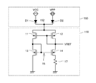
- FIG. 4 is a circuit diagram illustrating a configuration example of a VREF generation circuit 118 and a power supply selection circuit 150 in FIG. 3.
- FIG. 4 is a circuit diagram illustrating a configuration example of a VDC circuit 120 in FIG. 3.
- FIG. 4 is a circuit diagram illustrating a configuration example of a voltage detection circuit 122 in FIG. 3.
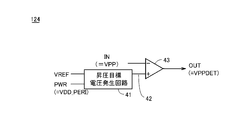
- FIG. 4 is a block diagram showing a voltage detector 124 in FIG. 3.
- FIG. 4 is a circuit diagram illustrating a configuration example of a discharge command holding circuit 128 in FIG. 3.
- FIG. 4 is a circuit diagram illustrating a configuration example of a discharge circuit 126 in FIG. 3.
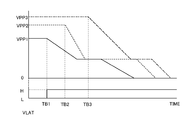
- FIG. 4 is a circuit diagram showing a configuration example of a modified example of the discharge circuit 126 in FIG. 3. It is a figure for demonstrating the discharge operation
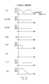
- FIG. 6 is a diagram illustrating waveforms of output signals in a state where VCC is constant without boosting operation in the first embodiment. 6 is a diagram illustrating waveforms of output signals in a state where VCC is cut off during a boost operation in the first embodiment.
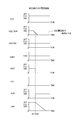
- FIG. 6 is a diagram illustrating waveforms of output signals in a state where VCC is cut off during a boost operation in the first embodiment.
- FIG. 6 is a diagram illustrating waveforms of output signals in a state where VCC is momentarily interrupted (instantaneous power failure) during boosting operation in the first embodiment.
- FIG. 6 is a diagram illustrating waveforms of output signals in a state where VDD is cut off during a boost operation in the first embodiment.
- FIG. 6 is a diagram illustrating waveforms of output signals in a state where VDD is momentarily interrupted (instantaneous power failure) during boosting operation in the first embodiment.
- FIG. 6 is a block diagram for explaining a flash memory 2B of a second embodiment.
- FIG. 19 is a circuit diagram illustrating a configuration example of a VREF generation circuit 218 in FIG. 18.
- FIG. 19 is a circuit diagram illustrating a configuration example of a VREF generation circuit 218 in FIG. 18.
- FIG. 19 is a circuit diagram showing a configuration example of a discharging VDC circuit 220B in FIG.
- FIG. 11 is a diagram illustrating waveforms of output signals in a state where VCC is constant and no boost operation is performed in the second embodiment.
- FIG. 10 is a diagram illustrating waveforms of output signals in a state where VCC is cut off during a boost operation in the second embodiment. It is a figure which shows the waveform of each output signal in the state in which VCC was instantaneously blacked out (instantaneous power failure) during boosting operation in the second embodiment.
- FIG. 10 is a diagram illustrating waveforms of output signals in a state where VDD is cut off during a boost operation in the second embodiment.
- FIG. 11 is a diagram illustrating waveforms of output signals in a state where VCC is constant and no boost operation is performed in the second embodiment.
- FIG. 10 is a diagram illustrating waveforms of output signals in a state where VCC is cut off during a boost
- FIG. 10 is a diagram illustrating waveforms of output signals in a state where VDD is momentarily interrupted (instantaneous power failure) during boosting operation in the second embodiment.
- FIG. 6 is a block diagram for illustrating a configuration of a flash memory 2C according to a third embodiment. It is a circuit diagram for demonstrating the structure of the power supply selection circuit 330 and the discharge VDC circuit 320B.
- FIG. 11 is a diagram showing waveforms of output signals in a state where VCC is constant and boosting operation is not performed in the third embodiment.
- FIG. 10 is a diagram illustrating waveforms of output signals in a state where VCC is cut off during a boost operation in the third embodiment.
- FIG. 10 is a diagram illustrating waveforms of output signals in a state where VDD is cut off during a boosting operation in the third embodiment.
- FIG. 11 is a diagram illustrating waveforms of output signals in a state where VDD is momentarily interrupted (instantaneous power failure) during boosting operation in the third embodiment.
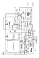
- FIG. 1 is a block diagram showing the overall configuration of the semiconductor device.
- a semiconductor device 1 includes a flash memory 2A, a functional block group 3, and a CPU 4.
- the functional block group includes various circuits such as an A / D converter, an interrupt controller, and a clock pulse generator.
- the flash memory 2A will be described more specifically.
- the external power supply voltage VCC, the internal power supply voltage VDD, and the boosted power supply voltage VPP may be referred to as VCC, VDD, and VPP, respectively.
- FIG. 2 is a block diagram for explaining the configuration of the flash memory 2 in the examination example.
- each circuit constituting the flash memory 2 will be briefly described. Detailed contents of each circuit will be described in the first embodiment.
- the flash memory 2 includes a flash memory core 110 and a Col control circuit 112 and a Row control circuit 114 that control the flash memory core 110 to be read from, written to, and erased from the flash memory core 110. Including.
- the flash memory 2 includes a VREF generation circuit 118 that generates a reference voltage VREF, a VDC circuit 120 (Voltage Down Converter circuit) that generates VDD, and a reference voltage VREF generated from the VREF generation circuit 118, thereby comparing VDD and VCC. And a voltage detection circuit 122 for detecting the level of the voltage.
- the flash memory 2 includes a VDD external input terminal 121 that can supply VDD from the outside instead of the VDC circuit 120. By using this VDD external input terminal 121, an internal power supply voltage can be easily supplied.
- the flash memory 2 includes a booster circuit 116 that generates a high voltage especially during writing and erasing, a voltage detector 124 that detects whether or not the VPP boosted by the booster circuit 116 is at a desired level, and a voltage detector 124. And a boost control circuit 130 for receiving respective output signals of the discharge command holding circuit 128.
- Boost control circuit 130 includes an inverter 123 that receives the output signal of voltage detector 124, and a NOR circuit 125 that receives the output signal of inverter 123 and the output signal of the discharge command holding circuit.
- flash memory 2 includes a discharge command holding circuit 128 that receives an output signal detected by voltage detection circuit 122, and a discharge circuit 126 that receives an output signal of the discharge command holding circuit.
- the discharge operation related circuit C0 includes a discharge circuit 126, a voltage detection circuit 122, and a discharge command holding circuit 128.
- VCC is an operating power supply voltage for the VREF generation circuit 118 and the VDC circuit 120 for generating VDD.
- VDD operates to drive the voltage detection circuit 122, the voltage detector 124, the discharge circuit 126, and the discharge command holding circuit 128. Power supply voltage.
- the VDD and the reference voltage VREF supplied when the VCC is powered off are insufficient as the operation power supply voltage and the reference voltage for the circuit that drives the discharge operation.
- the reference voltage VREF is used in the voltage detection circuit 122 and the voltage detector 124, but has a voltage value lower than the normal reference voltage VREF and is insufficient as a reference voltage.
- the discharge operation related circuit C0 As an example of the discharge operation related circuit C0, a configuration including the voltage detection circuit 122, the discharge circuit 126, and the discharge command holding circuit 128 is shown, but the configuration is not particularly limited thereto.
- FIG. 3 is a block diagram for explaining the configuration of the flash memory 2A of the first embodiment.
- flash memory 2A includes a power supply selection circuit 140 and a power supply selection circuit 150 in addition to the configuration of flash memory 2 shown in FIG.
- the configuration of each circuit of the flash memory 2A will be described.
- the power supply selection circuit 140 includes a diode D3 having the voltage VDD_PERI coupled to the anode and a diode D4 having the VPP coupled to the anode.
- the diode D3 and the cathode of the diode D4 are both connected to the node 142.
- the diode included in the power supply selection circuit 140 can be replaced with an element having a rectifying function. For example, it can be realized by a diode-connected transistor.
- FIG. 4 is a circuit diagram showing a configuration example of the VREF generation circuit 118 and the power supply selection circuit 150 in FIG.
- VREF generation circuit 118 receives reference voltage VREF at its gate, PMOS transistor 11 whose source is connected to a node supplied with power by power supply selection circuit 150, and reference voltage VREF at its gate and drain.
- a PMOS transistor 12 whose receiving source is connected to a node to which power is supplied by the power supply selection circuit 150, an NMOS transistor 13 whose drain is connected to the gate and drain, and whose source is connected to the ground node, and PMOS
- the transistor 11 includes an NMOS transistor 14 having a drain connected to the gate and a source connected to the resistor 17, and a resistor 17 connected between the source of the NMOS transistor 14 and the ground node.
- Power supply selection circuit 150 includes a diode D1 with VCC coupled to the anode and a diode D2 with VPP coupled to the anode, and the cathodes of diode D1 and diode D2 are both connected to the sources of PMOS transistor 11 and PMOS transistor 12. Is done.
- the diode included in the power supply selection circuit 150 is replaced with an element having a rectifying function. For example, it can be realized by a diode-connected transistor.
- the VREF generation circuit 118 is a circuit that outputs a constant voltage without being voltage-dependent if the supply power supply voltage maintains a certain potential.
- the power supply selection circuit 150 supplies a higher power supply voltage of VCC or VPP as the operation power supply voltage of the VREF generation circuit 118.
- FIG. 5 is a circuit diagram showing a configuration example of the VDC circuit 120 in FIG. Referring to FIG. 5, VDC circuit 120 receives and compares reference voltage VREF and the output voltage of VDC circuit 120, and a power supply node that receives the output of differential amplifier 22 at its gate and receives VCC. And a PMOS transistor 24 connected between the output node for outputting VDD. As long as VCC is supplied, the VDC circuit 120 outputs VDD having the voltage value of the reference voltage VREF.
- FIG. 6 is a circuit diagram showing a configuration example of the voltage detection circuit 122 in FIG.
- the voltage detection circuit 122 includes a voltage distribution unit 31 that distributes the input voltage IN1, a differential amplifier 32 that receives and compares the distribution voltage VDIV1 and the reference voltage VREF, and an output of the differential amplifier 32.
- OR circuit 38 for receiving is a circuit diagram showing a configuration example of the voltage detection circuit 122 in FIG.
- the voltage detection circuit 122 includes a voltage distribution unit 31 that distributes the input voltage IN1, a differential amplifier 32 that receives and compares the distribution voltage VDIV1 and the reference voltage VREF, and an output of the differential amplifier 32.
- OR circuit 38 for receiving.
- the voltage detection circuit 122 further includes a differential amplifier 36 that receives the reference voltage VREF and the output voltage of the differential amplifier 36, a voltage distribution unit 35 that distributes the output voltage of the differential amplifier 36, a distribution voltage VDIV2, and an input voltage IN2. And an OR circuit 38, one input node receiving the output signal of the differential amplifier 32 and the other input node receiving the output signal of the differential amplifier 34.
- the voltage distribution unit 31 includes a resistor 31A and a resistor 31B connected in series between the input voltage IN1 and the ground node, and outputs a distribution voltage VDIV1 input to the differential amplifier 32 according to the ratio of these resistors.
- the voltage distribution unit 35 includes a resistor 35A and a resistor 35B connected in series between the output voltage of the differential amplifier 36 and the ground node, and the distribution voltage VDIV2 input to the differential amplifier 34 according to the ratio of these resistors. Output. Note that the ratio of the resistances of the voltage distribution units 31 and 35 can be changed and designed according to the user's selection.
- the voltage detection circuit 122 can easily compare two kinds of power supply voltages with the reference voltage VREF.
- FIG. 7 is a block diagram showing the voltage detector 124 in FIG. Referring to FIG. 7, it includes a boost target voltage generation circuit 41 that receives reference voltage VREF and an operating power supply voltage, and a differential amplifier 43 that receives the output voltage of VPP and boost target voltage generation circuit 41.
- the output signal of the differential amplifier 43 becomes H level. That is, a boost command is issued, and the boost operation is started by the boost circuit.
- FIG. 8 is a circuit diagram showing a configuration example of the discharge command holding circuit 128 in FIG.
- the circuit configuration of discharge command holding circuit 128 is a so-called RS flip-flop circuit.
- the discharge command holding circuit 128 receives a signal VDET from the voltage detection circuit 122 and a reset signal RST from the system (for example, the CPU 4).
- a signal VLAT of the discharge command holding circuit 128 indicates a discharge command.
- the discharge command can be held, and the discharge operation can be performed until the high-voltage charge is completely discharged.
- FIG. 9 is a circuit diagram showing a configuration example of the discharge circuit 126 in FIG.
- discharge circuit 126 includes a discharge sequence control circuit 61S and an NMOS transistor 611.
- Discharge sequence control circuit 61S receives signal VLAT of discharge command holding circuit 128 as input signal EN.
- An output signal 61A from the discharge sequence control circuit 61S is input to the gate of the NMOS transistor 611.
- NMOS transistor 611 receives output signal 61A at its gate, its source is connected to VPP, and its drain is connected to the ground node.
- the NMOS transistor When the output signal 61A is at the L level, the NMOS transistor remains in the off state, so that the boosted charge is not discharged but is maintained.
- the discharge sequence control circuit can freely control the discharge of the VPP charge.
- FIG. 10 is a circuit diagram showing a configuration example of a modification of discharge circuit 126 in FIG.
- discharge circuit 126A includes a discharge sequence control circuit 62S and NMOS transistors 621 to 623.
- the discharge sequence control circuit 62S receives the signal VLAT of the discharge command holding circuit 128 as an input signal EN.
- Output signals 62A to 62C from the discharge sequence control circuit 62S are input to the gates of the NMOS transistors 621 to 623, respectively.
- NMOS transistors 621 to 623 receive output signals 62A to 62C at their gates, have their sources connected to VPP1 to VPP3, and their drains connected to the ground node.
- the discharge sequence control circuit 62S sets the start time of each discharge operation and sets the order of the NMOS transistors 621 to 623 that discharge the residual charges Control.
- FIG. 11 is a diagram for explaining a discharge operation by the discharge circuit 126 of FIG.
- VPP which is a voltage higher than the ON breakdown voltage of the transistor element
- the discharge sequence control circuit 61S controls such a stepwise discharge operation.
- signal VLAT is switched from L level to H level, and the discharge command is activated. Accordingly, the VPP charge on the drain side of the NMOS transistor 611 is changed from the L level to the H level by the output signal 61A, so that the NMOS transistor 611 is turned on and discharged until time TA2.
- the discharge sequence control circuit 61S switches the output signal 61A input to the gate to the N-channel MOS transistor 611 from the H level to the L level, so that the NMOS transistor 611 is turned off and the discharge operation is stopped. To do. Thereby, a voltage higher than the ON breakdown voltage of the transistor is not applied, and the transistor is not physically destroyed.
- the discharge operation is completed at time TA4 by discharging the remaining charge by switching the output signal 61A from the L level to the H level.
- FIG. 12 is a diagram for explaining a discharge operation by the discharge circuit 126A of FIG.
- a plurality of boosted power supply voltages are used inside the flash memory, and the parasitic capacitances of the boosted power supply voltage lines are also different. Therefore, when the discharge operation is simply started, the potential difference between the boosted power supply voltages widens due to the different discharge speeds, and a voltage higher than the on-withstand voltage of the transistor element is applied, or the relationship between the boosted power supply voltages is reversed during the discharge operation. If forward bias is generated, stored data and devices may be destroyed.
- a safe and accurate discharge operation is performed by controlling the discharge start timing of the charge of each boosted power supply voltage, the interval between the discharge operations, and the wait time according to the discharge operation sequence.
- the discharge of the charge at VPP1 is started from time TB1 and the discharge of the charge at VPP2 is started from time TB2. Then, discharge of the charge of VPP3 is started from time TB3.
- each discharge operation is stopped by the discharge sequence control circuit so that the relationship between each boosted power supply voltage is not reversed or the potential difference between the boosted power supply voltages is not opened too much. As a result, a forward bias or a voltage higher than the ON breakdown voltage of the transistor is not applied, and the transistor is not physically destroyed.
- the booster circuit 116 receives the output signal of the booster control circuit 130 as an input signal EN, boosts VCC using the voltage VDD_PERI as an operation power supply voltage, and generates a boosted power supply voltage VPP.
- the booster circuit 116 is a circuit that generates a voltage n times the power supply voltage (for example, VCC).
- the output voltage of the booster circuit 116 is controlled by the voltage detector 124, and when the booster voltage becomes equal to or higher than the boost target voltage, the boost operation is stopped. In addition, when the voltage becomes lower than the boost target voltage, the current boost power supply voltage is boosted to the boost target voltage by starting the boost operation.
- the booster circuit 116 When the supply power supply voltage drops and (supply power supply voltage) ⁇ (n times) ⁇ (boost target voltage), the booster circuit 116 always performs a boosting operation to obtain a voltage n times the supply power supply voltage. Try to output.
- the boost control circuit 130 deactivates the boost circuit 116, so that the voltage level of the boost power supply voltage is It fluctuates dynamically and the boosted power supply voltage drops according to the current consumption.
- boost control circuit 130 includes an inverter 123 and a NOR circuit 125.
- An output signal from the voltage detector 124 is input to the gate of the inverter 123, and an inverted signal that is an output signal of the inverter is input to one input node of the NOR circuit 125. Further, the output signal of the discharge command holding circuit 128 is input to the other input node of the NOR circuit 125.
- the signal VLAT is also transmitted to the system (for example, the CPU 4).
- the booster circuit 116 performs the boosting operation.
- the discharge operation related circuit C1 includes the discharge circuit 126, the voltage detection circuit 122, and the discharge command holding circuit 128 described above.
- power supply selection circuit 150 selects a higher power supply voltage of VCC or VPP, and VREF generation circuit 118 generates reference voltage VREF using the power supply voltage.
- VREF is normally supplied as long as the charge of VPP remains.
- the voltage detection circuit 122 detects a voltage drop of VCC or the voltage VDD_PERI, it outputs a signal VDET that is a discharge command.
- the discharge command holding circuit 128 latches the signal VDET which is this discharge command, and the boosting operation of the booster circuit 116 is stopped.
- the discharge circuit 126 discharges the charge of VPP according to the discharge sequence.
- the power supply selection circuit 140 selects the higher one of the voltage VDD_PERI and VPP. Using the selected power supply voltage, the operating power supply voltage is supplied to the voltage detection circuit 122, the discharge command holding circuit 128, and the discharge circuit 126 within a normal range. As a result, even if a voltage drop of VCC or voltage VDD_PERI occurs, the charge of VPP is discharged in the discharge circuit 126 according to the discharge sequence as long as the charge of VPP remains.
- the signal VLAT is also transmitted to the system (for example, the CPU 4), and the system recognizes that the flash memory 2A has started the discharge operation according to the discharge sequence, and processes the interrupted program.
- the reset signal (H level) is input to the discharge command holding circuit 128, the signal VLAT is switched to the L level, and the discharge operation ends.
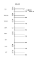
- FIG. 13 is a diagram showing the waveform of each output signal when the boosting operation is not performed and the VCC is constant in the first embodiment.
- FIG. 13 shows VCC, voltage VDD_PERI, voltage VDD_DIS, reference voltage VREF, signal VDET, signal RST, signal VLAT, and VPP in FIG. 3 in order from the top.
- VPP1, VCC1, and VDD1 the voltage values of VPP, VCC, and VDD are shown as VPP1, VCC1, and VDD1, respectively, from the top.
- time is shown on the horizontal axis.
- the output terminal of the VDC circuit 120 and the switch 141 will be described. However, the same applies to the case where the VDD external input terminal 121 and the switch 141 are connected. Further, since the discharge operation is not terminated by the system (for example, CPU 4), the signal RST from the system (for example, CPU 4) is set to the L level.
- This state is, for example, a state in which no write or erase operation is performed on the flash memory. In this state, VCC is not shut off or has a momentary power failure, and therefore has a constant voltage value VCC1.
- the voltage VDD_PERI is output by the VDC circuit 120 using VCC as an operation power supply voltage.
- the voltage value of the voltage VDD_PERI is VDD1.
- the power supply selection circuit 140 selects the higher one of the VPP and the voltage VDD_PERI.
- the power supply selection circuit 140 causes the voltage value of the voltage VDD_DIS to be the same as VDD1.
- the power supply selection circuit 150 selects the higher one of VCC and VPP. Therefore, since the step-up operation is not performed, the VREF generation circuit 118 supplies a constant reference voltage VREF with VCC as the operation power supply voltage.
- the voltage value of the reference voltage VREF at this time is VDD1.
- the voltages VDD_PERI and VCC are inputted, and the voltage VDD_DIS is used as the operation power supply voltage. Since the voltages VDD_PERI and VCC are higher than the reference voltage VREF, the signal VDET is at the H level. The voltage value is VDD1.
- an L level signal RST is input from the system (for example, CPU 4), an H level signal VDET is input from voltage detection circuit 122, and further, voltage VDD_DIS is input as an operating power supply voltage. . Since there is no step-up operation, signal VLAT from discharge command holding circuit 128 is at L level.
- the voltage value of the VPP becomes the voltage VDD_PERI.
- the voltage value of the voltage VDD_PERI is VDD1.
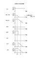
- FIG. 14 is a diagram showing waveforms of output signals in a state where VCC is cut off during the boosting operation in the first embodiment.
- this state corresponds to a state in which the user unplugs the power cord at a certain moment.
- VCC is cut off at time t0, and the voltage value of VCC gradually decreases.
- VCC falls below the VCC voltage drop detection level of the voltage detection circuit 122 at time t1, the voltage detection circuit 122 detects a VCC voltage drop.
- the voltage VDD_PERI is output from the VDC circuit 120 using VCC as the operating power supply voltage until time t1.
- the voltage value is VDD1.
- the voltage VDD_PERI also drops in the same manner as the VCC voltage drop.
- the power supply selection circuit 140 selects the higher one of the VPP and the voltage VDD_PERI. Therefore, until time t1, the voltage VDD_DIS takes VPP1, and thereafter the voltage drops following the voltage drop of VPP due to the discharge operation.
- the power supply selection circuit 150 selects the higher one of VCC and VPP. Accordingly, the constant reference voltage VREF is continuously supplied until time t2 (the voltage drop of VPP due to the discharge operation becomes the reference voltage VREF of the voltage value VDD1). Thereafter, the reference voltage VREF also drops with the voltage drop of VPP.
- the voltages VDD_PERI and VCC are inputted, and the voltage VDD_DIS is used as the operation power supply voltage.
- the signal VDET remains at the H level until time t1. After time t1, since VCC falls below the VCC voltage drop detection level, this is detected and the signal VDET switches from the H level to the L level.
- L level signal RST is input from the system (for example, CPU 4)
- H level signal VDET is input from voltage detection circuit 122
- voltage VDD_DIS is input as an operating power supply voltage.
- the signal VLAT from the discharge command holding circuit 128 also switches from the L level to the H level. Then, after time t1, the signal VLAT also drops with a voltage drop of the voltage VDD_DIS.
- the signal VLAT is input to the system (for example, the CPU 4), the discharge circuit 126, and the boost control circuit 130.
- an L level output signal is input from the boost control circuit 130 to the boost circuit 116, and the boost operation of the boost circuit 116 is stopped.
- the discharge circuit 126 discharges the charge of VPP according to the discharge sequence.
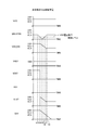
- FIG. 15 is a diagram showing waveforms of output signals in a state where VCC is momentarily interrupted (instantaneous power failure) during the boosting operation in the first embodiment.
- the vertical axis, horizontal axis, scale, setting of signal RST and connection relationship of switch 141 are the same as those in FIG.
- a power supply voltage is not instantaneously supplied due to a natural disaster such as a system (for example, the CPU 4) or a lightning, and the state after the recovery is applied.
- the time between t3 and t8 is shown as the time of VCC instantaneous power failure. Specifically, at time t3, the VCC voltage drop starts. At time t4, VCC falls below the VCC voltage drop detection level, and VCC continues to drop until time t5. At time t5, the voltage drop of VCC stops. After time t5, the voltage of VCC rises again, and at time t6, VCC exceeds the VCC voltage drop detection level. After time t8, VCC returns to the voltage value before time t3.
- the voltage VDD_PERI is output from the VDC circuit 120 with VCC as the operating power supply voltage until time t4 and after time t6.
- the voltage value is a constant voltage value VDD1. From time t4 to time t6, the voltage VDD_PERI causes a similar voltage change as the VCC voltage changes.
- the power supply selection circuit 140 selects the higher one of the VPP and the voltage VDD_PERI until the time t4. Therefore, the voltage VDD_DIS takes VPP1, and the voltage VDD_DIS continues to drop with the voltage drop of VPP until the time t4 to t7.
- the voltage VDD_DIS becomes a constant voltage value VDD1 of the voltage VDD_PERI since the higher one of the VPP and the voltage VDD_PERI is selected after the time t7.
- the operation power supply voltage of the VREF generation circuit 118 is selected by the power supply selection circuit 150, whichever is higher, VPP or VCC. Accordingly, the VREF generation circuit 118 receives an operating power supply voltage equal to or higher than the voltage value VDD1, and supplies a constant reference voltage VREF.
- the voltage detection circuit 122 detects the VCC voltage drop, and the signal VDET switches from the H level to the L level.
- Signal VDET and L level signal RST from the system (for example, CPU 4) are input to discharge command holding circuit 128, and signal VLAT switches from L level to H level.
- the signal VLAT is input to the system (for example, the CPU 4), the discharge circuit 126, and the boost control circuit 130.
- an L level output signal is input from the boost control circuit 130 to the booster circuit 116, so that the boosting operation of the booster circuit 116 stops and the boosting operation of the booster circuit 116 stops.
- the discharge circuit 126 discharges the residual charge of VPP according to the discharge sequence.
- the operating power supply voltage of the discharge command holding circuit 128 becomes VPP. Therefore, the voltage of the signal VLAT also drops with the voltage drop of VPP.
- the operation power supply voltage becomes the voltage VDD_PERI and takes a constant voltage value VDD1.
- FIG. 16 is a diagram showing waveforms of output signals in a state where VDD is cut off during the boosting operation in the first embodiment.
- the vertical axis, horizontal axis, and scale are the same as those in FIG.
- the description will be made assuming that the VDD external input terminal 121 and the switch 141 are connected.
- the output terminal of the VDC circuit 120 and the switch 141 are connected, the description will not be repeated.
- the power supply of the VDD external input terminal 121 may be cut off.
- VCC Since VCC is not affected by the power shutdown of VDD, it becomes a constant voltage (voltage value VCC1).
- the VDD supplied from the VDD external input terminal 121 is cut off at time t10, and the voltage value of VDD gradually decreases. Accordingly, the voltage VDD_PERI connected by the switch 141 similarly starts to drop at time t10, falls below the VDD voltage drop detection level at time t11, and becomes the ground potential at time t12.
- the power supply selection circuit 140 selects the higher one of the VPP and the voltage VDD_PERI. Therefore, until time t11, VPP is selected by the power supply selection circuit 140, and the voltage VDD_DIS drops as well as the voltage drop of VPP due to the discharge operation.
- the power supply selection circuit 150 selects the higher power supply voltage of VCC or VPP as the operation power supply voltage. Therefore, the VREF generation circuit 118 is supplied with an operating power supply voltage equal to or higher than the voltage value VDD1, and supplies a constant reference voltage VREF.
- the voltages VDD_PERI and VCC are inputted, and the voltage VDD_DIS is used as the operation power supply voltage.
- the signal VDET remains at the H level until time t11. After time t11, VDD falls below the VDD voltage drop detection level, so this is detected and the signal VDET switches from the H level to the L level.
- L level signal RST is input from the system (for example, CPU 4)
- H level signal VDET is input from voltage detection circuit 122
- voltage VDD_DIS is input as an operating power supply voltage.
- the signal VLAT from the discharge command holding circuit 128 also switches from the L level to the H level. Then, after time t11, the signal VLAT drops with the voltage drop of the voltage VDD_DIS.
- the signal VLAT is input to the system (for example, the CPU 4), the discharge circuit 126, and the boost control circuit 130.
- an L level output signal is input from the boost control circuit 130 to the boost circuit 116, and the boost operation of the boost circuit 116 is stopped.
- the discharge circuit 126 discharges the residual charge of VPP according to the discharge sequence.
- FIG. 17 is a diagram illustrating waveforms of output signals in a state where VDD is momentarily interrupted (instantaneous power failure) during the boosting operation in the first embodiment.
- VDD momentarily interrupted
- FIGS. 3 and 17 the vertical axis, horizontal axis, scale, setting of signal RST, and connection relationship of switch 141 are the same as those in FIG.
- VDD when VDD is supplied from the VDD external input terminal 121, a case where the VDD external input terminal 121 is momentarily interrupted can be considered.
- VCC Since VCC is not affected by the instantaneous power failure of VDD, it becomes a constant voltage. Between time t13 and t18, it is shown as the time of instantaneous power failure of VDD.
- the voltage VDD_PERI is supplied from the external input terminal 121, the voltage change of the VDD is almost equal to the voltage change of the voltage VDD_PERI. Therefore, the waveforms are almost equal. Specifically, at time t13, a voltage drop of the voltage VDD_PERI is started. At time t14, the voltage VDD_PERI falls below the VDD voltage drop detection level and continues to drop until time t15. At time t15, the voltage drop of the voltage VDD_PERI stops.
- the voltage VDD_PERI rises again, and at time t16, the voltage VDD_PERI exceeds the VDD voltage drop detection level. After time t18, the voltage VDD_PERI returns to the voltage value before time t13.
- the voltage VDD_DIS becomes a constant voltage value VPP1 of VPP because the higher one of VPP and voltage VDD_PERI is selected as the operation power supply voltage by the power supply selection circuit 140 until time t4.
- the voltage VDD_DIS continues to drop with the voltage drop of VPP from time t14 to t17.
- the voltage VDD_DIS slightly increases after time t17 and becomes a constant voltage value VDD1 after time t18. The reason is that the power supply selection circuit 140 selects the higher one of the VPP and the voltage VDD_PERI. Specifically, until time t17, (voltage value of VPP)> (voltage value of voltage VDD_PERI), and after time t17, (voltage value of voltage VDD_PERI)> (voltage value of VPP).
- the power supply selection circuit 150 selects the higher one of VPP and VCC, the operation power supply voltage of the VREF generation circuit 118 is higher than the reference voltage VREF, so that the reference voltage VREF is constant.
- the voltage value is VDD1.
- the voltage detection circuit 122 detects the voltage drop of the voltage VDD_PERI, and the signal VDET switches from the H level to the L level.
- Signal VDET and an L level signal from the system are input to discharge command holding circuit 128, and signal VLAT is switched from the L level to the H level.
- the signal VLAT is input to the system (for example, the CPU 4), the discharge circuit 126, and the boost control circuit 130.
- an L level output signal is input from the boost control circuit 130 to the booster circuit 116, so that the boosting operation of the booster circuit 116 stops and the boosting operation of the booster circuit 116 stops.
- the discharge circuit 126 discharges the residual charge of VPP according to the discharge sequence.
- the operation power supply voltage of the discharge command holding circuit 128 becomes VPP. Therefore, the voltage of the signal VLAT also drops with the voltage drop of VPP.
- the operating power supply voltage becomes the voltage VDD_PERI and takes a constant voltage value VDD1.
- the circuit related to the discharge operation operates from VPP.
- the boosted charge is normally discharged.
- destruction of stored data and physical destruction of the device can be avoided.
- a capacitor for controlling the discharge operation is not necessary. It should be noted that even in a non-volatile memory other than the flash memory, it is possible to avoid the destruction of stored data and the physical destruction of the device by adopting the same configuration.
- the discharge operation related circuit C2 includes a discharge VDC circuit 220B in addition to the discharge operation related circuit C1.
- the discharge VDC circuit 220B supplies an operating power supply voltage to the discharge circuit 126, the voltage detection circuit 122, and the discharge command holding circuit 128.
- FIG. 18 is a block diagram for explaining the flash memory 2B of the second embodiment.
- flash memory 2 ⁇ / b> B replaces power supply selection circuit 150, VREF generation circuit 218 instead of VREF generation circuit 118, and VDC circuit 120.
- the configuration of each circuit of the flash memory 2B will be described.
- FIG. 19 is a circuit diagram showing a configuration example of the VREF generation circuit 218 in FIG. Referring to FIG. 19, VREF generation circuit 218 receives a reference voltage VREF at its gate, PMOS transistor 11 whose source is connected to a node supplied with power by power supply selection circuit 150, and reference voltage VREF at its gate and drain.
- a PMOS transistor 12 whose receiving source is connected to a node to which power is supplied by the power supply selection circuit 150, an NMOS transistor 13 whose drain is connected to the gate and drain, and whose source is connected to the ground node, and PMOS
- the transistor 11 includes an NMOS transistor 14 having a drain connected to the gate and a source connected to the resistor 17, and a resistor 17 connected between the source of the NMOS transistor 14 and the ground node.
- Power supply selection circuit 150 includes a diode D1 with VCC coupled to the anode and a diode D2 with VPP coupled to the anode, and the cathodes of diode D1 and diode D2 are both connected to the sources of PMOS transistor 11 and PMOS transistor 12. Is done.
- the diode included in the power supply selection circuit 150 can be replaced with an element having a rectifying function. For example, it can be realized by a diode-connected transistor.
- the VREF generation circuit 218 further includes a differential amplifier 82 that receives the reference voltage VREF and the output of the differential amplifier 82, and a voltage distribution unit 83 that distributes the output voltage of the differential amplifier 82.
- the voltage distribution unit 83 includes a resistor 83A and a resistor 83B connected in series between the output voltage of the differential amplifier 36 and the ground node, and outputs the reference voltage VREF- ⁇ distributed according to the ratio of these resistors.
- the resistance ratio of the voltage distribution unit 83 can be designed by changing according to the user's selection.
- the reference voltage VREF- ⁇ is lower than the reference voltage VREF and higher than the power supply voltage that allows the discharge circuit 126, the discharge command holding circuit 128, and the voltage detection circuit 122 to operate normally.
- the VREF generation circuit 218 is a circuit that outputs two types of constant voltages without receiving voltage dependency if the supply power supply voltage maintains a certain potential. Specifically, the reference voltage VREF and the reference voltage VREF- ⁇ .
- the reference voltage VREF is input to the voltage detector 124 and the voltage detection circuit 122 related to the discharge operation. In addition, the signal is also input to the peripheral VDC circuit 220A and the discharge VDC circuit 220B.
- the reference voltage VREF- ⁇ is input to the discharging VDC circuit 220B.
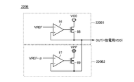
- FIG. 20 is a circuit diagram showing a configuration example of the discharging VDC circuit 220B in FIG.
- discharging VDC circuit 220B includes a VDC circuit 220B1 and a VDC circuit 220B2.
- the VDC circuit 220B1 and the VDC circuit 220B2 are connected in parallel to output the voltage VDD_DIS.
- the VDC circuit 220B1 receives and compares the reference voltage VREF as a reference for the voltage VDD_DIS and the voltage VDD_DIS, the differential amplifier 86 receives the output of the differential amplifier 86 at the gate, and outputs the power supply node receiving VCC and the voltage VDD_DIS.
- PMOS transistor 88 connected to the output node.
- the VDC circuit 220B2 receives and compares the reference voltage VREF- ⁇ as a reference of the voltage VDD_DIS and the voltage VDD_DIS, the differential amplifier 87 receiving the output of the differential amplifier 87, the power supply node receiving the VPP, and the voltage VDD_DIS PMOS transistor 89 connected between the output node for output.
- peripheral VDC circuit 220A has the same configuration as VDC circuit 120 in FIG. 2, description thereof will not be repeated.
- the operation power supply voltage of VREF generation circuit 218 is selected by power supply selection circuit 150 by selecting the higher power supply voltage of VCC or VPP, and VREF generation circuit 218 uses the power supply voltage.
- a reference voltage VREF and a reference voltage VREF- ⁇ are generated. As a result, even if the voltage drop of VCC occurs, the reference voltage VREF and the reference voltage VREF- ⁇ are normally supplied as long as the charge of VPP remains.
- the voltage value of the voltage VDD_DIS is the reference voltage.
- VREF- ⁇ can be output, and an operation power supply voltage can be supplied to a circuit related to the discharge operation.
- the discharge command holding circuit 128 latches the discharge command (signal VDET), and the booster circuit 116 stops.
- the discharge circuit 126 discharges the charge of VPP according to the discharge sequence.
- the operating power supply voltage of the voltage detection circuit 122 and the discharge command holding circuit 128 is supplied from the voltage VDD_DIS. Therefore, when (VPP voltage value)> (reference voltage VREF ⁇ voltage value), the discharge sequence control circuit operates normally.
- the signal VLAT is also transmitted to the system (for example, the CPU 4), and the system recognizes that the flash memory 2B has entered the discharging operation, and processes the interrupted program.
- the signal VLAT is switched to the L level, and the discharge operation ends.
- Embodiment 2 can avoid the physical destruction of the data stored in the flash memory and the device even when there is a power interruption or a momentary power failure.
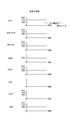
- FIG. 21 is a diagram showing the waveform of each output signal when the boosting operation is not performed and the VCC is constant in the second embodiment.
- This state is, for example, a state in which no write or erase operation is performed on the flash memory.
- VCC voltage VDD_PERI, voltage VDD_DIS, reference voltage VREF, signal VDET, signal RST, signal VLAT, and VPP in FIG. 18 are shown in order from the top.
- VCC Since VCC has not been cut off or instantaneous power failure, it has a constant voltage value VCC1.
- the voltage VDD_PERI is output by the peripheral VDC circuit 220A using VCC as an operation power supply voltage.
- the voltage value is VDD1.
- the circuit configurations of the peripheral VDC circuit 220A and the VDC circuit 120 are the same.
- the voltage VDD_DIS is output by the discharging VDC circuit 220B.
- the power supply selection circuit 150 selects the higher one of VCC and VPP.
- VREF generation circuit 118 supplies a constant reference voltage VREF with VCC as the operation power supply voltage.
- the voltage value of the reference voltage VREF at this time is VDD1.
- the voltages VDD_PERI and VCC are inputted, and the voltage VDD_DIS is used as the operation power supply voltage. Since the voltages VDD_PERI and VCC are higher than the reference voltage VREF, the signal VDET is at the H level. The voltage value is VDD1.
- L level signal RST from the system (for example, CPU 4) is input, H level signal VDET is input from voltage detection circuit 122, and voltage VDD_DIS is input as the operating power supply voltage. Since there is no step-up operation, signal VLAT from discharge command holding circuit 128 is at L level.
- the voltage value of the VPP becomes the voltage VDD_PERI.
- the voltage value of the voltage VDD_PERI is VDD1.
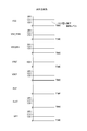
- FIG. 22 is a diagram showing waveforms of output signals in a state where VCC is cut off during the boosting operation in the second embodiment.
- VCC is cut off at time t20, and VCC1, which is the voltage value of VCC, gradually decreases.
- VCC1 which is the voltage value of VCC
- the voltage detection circuit 122 detects the voltage drop of VCC.
- the voltage VDD_PERI is output from the peripheral VDC circuit 220A using VCC as the operating power supply voltage until time t21.
- the voltage value is VDD1.
- the voltage VDD_PERI drops as well as the voltage drop of VCC.
- the voltage value of the voltage VDD_PERI drops from VDD1 to the ground potential.
- the voltage VDD_DIS takes the same voltage as the reference voltage VREF from the VDC circuit 220B1 of FIG. 20 until time t21. After time t21, voltage VDD_DIS takes the same voltage as reference voltage VREF- ⁇ by VDC from VDC circuit 220B2 in FIG.
- the power supply selection circuit 150 selects the higher one of VCC or VPP. Accordingly, the reference voltage VREF having a constant voltage is supplied until the voltage drop of VPP due to the discharge operation reaches the VCC level. Thereafter, when the voltage value of VPP becomes equal to or lower than the reference voltage VREF, the reference voltage VREF cannot supply a constant voltage, and the voltage drops.
- the voltages VDD_PERI and VCC are inputted, and the voltage VDD_DIS is used as the operation power supply voltage. Since VCC has exceeded the VCC voltage drop detection level until time t21, the signal VDET is at the H level. After time t21, VCC falls below the VCC voltage drop detection level, so this is detected and the signal VDET switches from H level to L level.
- L level signal RST is input from the system (for example, CPU 4)
- H level signal VDET is input from voltage detection circuit 122
- voltage VDD_DIS is input as an operating power supply voltage.
- the signal VLAT from the discharge command holding circuit 128 also switches from the L level to the H level.
- the signal VLAT also drops with the voltage change of the voltage VDD_DIS.
- the signal VLAT is input to the system (for example, the CPU 4), the discharge circuit 126, and the boost control circuit 130.
- an L level output signal is input from the boost control circuit 130 to the boost circuit 116, and the boost operation of the boost circuit 116 is stopped.
- the discharge circuit 126 discharges the residual charge of VPP according to the discharge sequence.
- FIG. 23 is a diagram illustrating waveforms of output signals in a state where VCC is momentarily interrupted (instantaneous power failure) during the boosting operation in the second embodiment.
- a power supply voltage is not instantaneously supplied due to a natural disaster such as a system (for example, CPU 4) or a lightning, and then a state in which the power supply is recovered is applicable.
- a natural disaster such as a system (for example, CPU 4) or a lightning
- time t23 and t27 it is shown as the time when VCC momentary power failure occurred. Specifically, at time t23, the voltage drop of VCC is started. At time t24, VCC falls below the VCC voltage drop detection level, and VCC continues to drop until time t25. At time t25, the voltage drop of VCC stops. After time t25, the voltage of VCC rises again, and at time t26, VCC exceeds the VCC voltage drop detection level. After time t27, VCC returns to the voltage value before time t23.
- the voltage VDD_PERI is output from the discharging VDC circuit 220A using VCC as an operating power supply voltage until time t24 and after time t26.
- the voltage value is a constant voltage value VDD1. From time t24 to t26, the voltage VDD_PERI changes in the same manner as the VCC voltage changes.
- the voltage VDD_DIS is output by the discharging VDC circuit 220B. Specifically, since there is no instantaneous power outage in VCC until time t24, voltage VDD_DIS becomes an output from VDC circuit 220B1 in FIG. The value is the same as the voltage value of the reference voltage VREF. From time t24 to t26, VCC falls below the VCC voltage drop detection level, so the voltage VDD_DIS becomes an output from the VDC circuit 220B2 of FIG. The value is the reference voltage VREF- ⁇ . After time t26, the voltage VDD_DIS is again output from the VDC circuit 220B1 in FIG. The value is the same as the voltage value of the reference voltage VREF.
- the reference voltage VREF has a constant voltage value even between time t24 and t26.
- the power supply selection circuit 150 selects the higher one of VPP and VCC. Since the reference voltage VREF does not fall below the voltage value, the reference voltage VREF is a constant voltage.
- the voltage value is VDD1.
- the voltage detection circuit 122 detects the VCC voltage drop, and the signal VDET switches from the H level to the L level.
- the signal VDET and the L level signal RST from the system are input to the discharge command holding circuit 128, and the signal VLAT is switched from the L level to the H level.
- the signal VLAT is input to the system (for example, the CPU 4), the discharge circuit 126, and the boost control circuit 130.
- an L level output signal is input from the boost control circuit 130 to the boost circuit 116, and the boost operation of the boost circuit 116 is stopped.
- the discharge circuit 126 discharges the residual charge of VPP according to the discharge sequence.
- FIG. 24 is a diagram showing waveforms of output signals in a state where VDD is cut off during the boosting operation in the second embodiment.
- the vertical axis, horizontal axis, and scale are the same as those in FIG.
- the description will be made assuming that the VDD external input terminal 121 and the switch 141 are connected.
- the output terminal of the peripheral VDC circuit 220A is connected to the switch 141, the description will not be repeated.
- the power supply of the VDD external input terminal 121 may be cut off.
- VCC Since VCC is not affected by the power shutdown of VDD, it becomes a constant voltage (voltage value VCC1).
- VDD supplied from the VDD external input terminal 121 is cut off at time t30, and the voltage value of VDD gradually decreases.
- VDD_PERI output from the peripheral VDC circuit 220A starts to drop at time t30, falls below the VDD voltage drop detection level at time t31, and becomes the ground potential at time t32.
- the voltage VDD_DIS is output from the discharging VDC circuit 220B using VCC as an operating power supply voltage. Since VCC always has a constant voltage value VCC1, the voltage VDD_DIS also has a constant voltage value VDD1.
- the power supply selection circuit 150 selects the higher one of VCC or VPP as the operation power supply voltage. However, since the selected power supply voltage never falls below the VCC voltage drop detection level, the reference voltage VREF is a constant voltage. The voltage value is VDD1.
- the voltages VDD_PERI and VCC are inputted, and the voltage VDD_DIS is used as the operation power supply voltage.
- the signal VDET remains at the H level. After time t31, since VDD is below the VDD voltage drop detection level, this is detected and the signal VDET switches from H level to L level.
- L level signal RST is input from the system (for example, CPU 4)
- H level signal VDET is input from voltage detection circuit 122
- voltage VDD_DIS is further input as the operating power supply voltage.
- the signal VLAT from the discharge command holding circuit 128 also switches from the L level to the H level.
- the signal VLAT level is also a constant value.
- the signal VLAT is input to the system (for example, the CPU 4), the discharge circuit 126, and the boost control circuit 130.
- an L level output signal is input from the boost control circuit 130 to the boost circuit 116, and the boost operation of the boost circuit 116 is stopped.
- the discharge circuit 126 discharges the residual charge of VPP according to the discharge sequence.
- FIG. 25 is a diagram illustrating waveforms of output signals in a state where VDD is momentarily interrupted (instantaneous power failure) during the boosting operation in the second embodiment.
- VDD when VDD is supplied from the VDD external input terminal 121, a case where the VDD external input terminal 121 is momentarily interrupted can be considered.
- VCC Since VCC is not affected by the instantaneous power failure of VDD, it becomes a constant voltage. Between the times t33 and t37, it is shown as the time of the momentary power failure of VDD.
- the voltage VDD_PERI is supplied from the external input terminal 121, the voltage change of the VDD and the voltage change of the voltage VDD_PERI are substantially equal, so the waveforms thereof are also substantially equal.
- a voltage drop of the voltage VDD_PERI is started at time t33.
- the voltage VDD_PERI falls below the VDD voltage drop detection level and continues to drop until time t35.
- the voltage drop of the voltage VDD_PERI stops.
- the voltage VDD_PERI rises again, and at time t36, the voltage VDD_PERI exceeds the VDD voltage drop detection level. After time t37, the voltage VDD_PERI returns to the voltage value before time t33.
- the voltage VDD_DIS is output from the discharging VDC circuit 220B using VCC as an operating power supply voltage. Since VCC has a constant voltage value VCC1, the voltage VDD_DIS also has a constant voltage value VDD1.
- the reference voltage VREF is output from the VREF generation circuit 218 using VCC as an operating power supply voltage. Since VCC has a constant voltage value VCC1, the reference voltage VREF also has a constant voltage value VDD1.
- the voltages VDD_PERI and VCC are inputted, and the voltage VDD_DIS is used as the operation power supply voltage.
- the signal VDET remains at the H level.
- VDD falls below the VDD voltage drop detection level, so this is detected and the signal VDET switches from the H level to the L level.
- L level signal RST is input from the system (for example, CPU 4)
- H level signal VDET is input from voltage detection circuit 122
- voltage VDD_DIS is further input as the operating power supply voltage.
- the signal VLAT from the discharge command holding circuit 128 switches from the L level to the H level.
- the signal VLAT level is also a constant value.
- the signal VLAT is input to the system (for example, the CPU 4), the discharge circuit 126, and the boost control circuit 130.
- an L level output signal is input from the boost control circuit 130 to the boost circuit 116, and the boost operation of the boost circuit 116 is stopped.
- the discharge circuit 126 discharges the residual charge of VPP according to the discharge sequence.
- the operation power supply voltage is received from the VPP.
- the reference voltage VREF and the reference voltage VREF- ⁇ are generated and supplied to a circuit related to the discharge operation, so that the boosted charge is normally discharged. This makes it possible to protect the data and device of the flash memory from the boosted voltage. Further, a capacitor for controlling the discharge operation is not necessary.
- FIG. 26 is a block diagram for explaining the configuration of the flash memory 2C of the third embodiment. This will be described in comparison with the configuration of the study example.
- flash memory 2C has a power supply selection circuit 150, a power supply selection circuit 330, and a peripheral VDC circuit 320A in place of VREF generation circuit 118. And a discharging VDC circuit 320B.
- the discharge operation related circuit C3 includes a discharge VDC circuit 320B in addition to the discharge operation related circuit C0.
- the discharge VDC circuit 320B supplies an operating power supply voltage to the discharge circuit 126, the voltage detection circuit 122, and the discharge command holding circuit 128.
- Power supply selection circuit 150 includes a diode D1 with VCC coupled to the anode and a diode D2 with VPP coupled to the anode, and the cathodes of diode D1 and diode D2 are both connected to node 152.
- the power supply selection circuit 330 includes a diode D5 in which VCC is coupled to the anode and a diode D6 in which VPP is coupled to the anode, and the cathodes of the diode D5 and the diode D6 are both connected to the node 332.
- the diode included in the power supply selection circuit 330 can be replaced with an element having a rectifying function. For example, it can be realized by a diode-connected transistor.
- FIG. 27 is a circuit diagram for explaining the configuration of the power supply selection circuit 330 and the discharging VDC circuit 320B.
- discharge VDC circuit 320B receives differential amplifier 96 that receives reference voltage VREF and voltage VDD_DIS for comparison, and the power supplied from power supply selection circuit 330 by receiving the output of differential amplifier 96 at the gate.
- a PMOS transistor 88 connected between a power supply node that receives the voltage and an output node that outputs voltage VDD_DIS is included.
- the power supply selection circuit 150 supplies the higher power supply voltage of either VCC or VPP to the VREF generation circuit 118 as the operation power supply voltage, and the reference voltage VREF having a constant voltage is supplied. Therefore, even if a voltage drop equal to or lower than the VCC reference voltage VREF occurs, if the voltage VPP is higher than the reference voltage VREF, the reference voltage VREF is supplied at a constant voltage.
- the voltage VDD_DIS becomes a constant voltage, and the circuit related to the discharge operation is set. Supply.
- the voltage value is VDD1.
- the signal VDET When the voltage detection circuit 122 detects a voltage drop of VCC or the voltage VDD_PERI, the signal VDET is switched from the L level to the H level. The boosting operation of the booster circuit 116 is stopped. On the other hand, the discharge circuit 126 discharges the charge of VPP according to the discharge sequence. These operating power supply voltages are supplied from the voltage VDD_DIS. For this reason, the discharge sequence control circuit operates normally while the constant voltage reference voltage VREF is supplied. The signal VLAT is notified to the system (for example, the CPU 4), and the system (for example, the CPU 4) recognizes that the flash memory 2C has entered the discharging operation, and processes the interrupted program. By sending a reset signal (H level) to the discharge command holding circuit 128, the signal VLAT is switched to the L level, and the discharge operation ends.
- a reset signal H level
- Embodiment 3 it is possible to avoid the physical destruction of the data stored in the flash memory and the device even when there is a power interruption or a momentary power failure.
- FIG. 28 is a diagram showing waveforms of output signals in a state where the boosting operation is not performed and VCC is constant in the third embodiment.
- This state is, for example, a state in which no write or erase operation is performed on the flash memory.
- FIG. 28 shows VCC, voltage VDD_PERI, voltage VDD_DIS, reference voltage VREF, signal VDET, signal RST, signals VLAT, and VPP in FIG. 26 in order from the top.
- VCC Since VCC has not been cut off or instantaneous power failure, it has a constant voltage value VCC1.
- the voltage VDD_PERI is output by the peripheral VDC circuit 320A using VCC as an operation power supply voltage.
- the voltage value is VDD1.
- the peripheral VDC circuit 320A and the VDC circuit 120 in FIG. 2 have the same circuit configuration.
- the voltage VDD_DIS is output by the discharging VDC circuit 320B.
- the power supply selection circuit 150 selects the higher one of VCC and VPP. Therefore, since the step-up operation is not performed, the VREF generation circuit 118 supplies a constant reference voltage VREF with VCC as the operation power supply voltage.
- the voltage value of the reference voltage VREF at this time is VDD1.
- the voltages VDD_PERI and VCC are inputted, and the voltage VDD_DIS is used as the operation power supply voltage. Since the voltages VDD_PERI and VCC are higher than the reference voltage VREF, the signal VDET is at the H level. The voltage value is VDD1.
- L level signal RST from the system (for example, CPU 4) is input, H level signal VDET is input from voltage detection circuit 122, and voltage VDD_DIS is input as the operating power supply voltage. Since there is no step-up operation, signal VLAT from discharge command holding circuit 128 is at L level.
- the voltage value of the VPP becomes the voltage VDD_PERI.
- the voltage value of the voltage VDD_PERI is VDD1.
- FIG. 29 is a diagram showing waveforms of output signals in a state where VCC is cut off during the boosting operation in the third embodiment.
- VCC is cut off at time t40 and VCC1, which is the voltage value of VCC, gradually decreases.
- VCC1 which is the voltage value of VCC
- the voltage detection circuit 122 detects the voltage drop of VCC.
- the voltage VDD_PERI is output from the peripheral VDC circuit 320A using VCC as an operating power supply voltage until time t41.
- the voltage value is VDD1.
- the voltage VDD_PERI also drops in the same manner as the VCC voltage drop.
- the voltage value drops from VDD1 to the ground potential.
- the power supply selection circuit 330 selects the higher one of VPP and VCC. Therefore, until time t42, VPP is selected by the power supply selection circuit 330, and the voltage VDD_DIS supplies a constant voltage to a circuit related to the discharge operation. However, after time t42, the power supply voltage VPP of the power supply selection circuit 330 drops due to the discharge operation, and VCC is already at the ground potential. Therefore, the voltage drop of VDD_DIS is the same as the voltage drop of VPP. From another point of view, even if the VCC power is cut off, the discharging operation is executed until time t42, and the destruction of the stored data and the physical destruction of the device can be avoided.
- the power supply selection circuit 150 selects the higher one of VCC and VPP. Therefore, the constant reference voltage VREF is supplied until the voltage drop of VPP due to the discharge operation reaches the VCC level. After time t42, the voltage value of VPP becomes equal to or lower than VDD1, the VREF generation circuit 118 cannot supply a constant voltage, and the reference voltage VREF drops.
- the voltages VDD_PERI and VCC are inputted, and the voltage VDD_DIS is used as the operation power supply voltage. Since VCC exceeds the VCC voltage drop detection level until time t41, the signal VDET is at the H level. After time t41, since VCC falls below the VCC voltage drop detection level, this is detected and the signal VDET switches from the H level to the L level.
- L level signal RST is input from the system (for example, CPU 4)
- H level signal VDET is input from voltage detection circuit 122
- voltage VDD_DIS is further input as the operating power supply voltage.
- the signal VLAT from the discharge command holding circuit 128 also switches from the L level to the H level. Then, after time t41, the signal VLAT level changes in the same manner as the voltage VDD_DIS changes.
- the signal VLAT is input to the system (for example, the CPU 4), the discharge circuit 126, and the boost control circuit 130.
- an L level output signal is input from the boost control circuit 130 to the boost circuit 116, and the boost operation of the boost circuit 116 is stopped.
- the discharge circuit 126 discharges the residual charge of VPP according to the discharge sequence.
- FIG. 30 is a diagram illustrating waveforms of output signals in a state where VCC is momentarily interrupted (instantaneous power failure) during the boosting operation in the second embodiment.
- the time between t43 and t47 is shown as the time of VCC instantaneous power failure. Specifically, at time t43, the VCC voltage drop starts. At time t44, VCC falls below the VCC voltage drop detection level, and VCC continues to drop between times t44 and t45. At time t45, the voltage drop of VCC stops. After time t45, the voltage of VCC rises, and at time t46, VCC exceeds the VCC voltage drop detection level. At time t47, VCC returns to a constant voltage value before time t43.
- the voltage VDD_PERI is output from the discharging VDC circuit 320A using VCC as the operating power supply voltage until time t44 and after time t46.
- the voltage value is a constant voltage value VDD1. From time t44 to t46, the voltage VDD_PERI changes in the same manner as the VCC voltage changes.
- the power supply selection circuit 330 selects the higher one of VCC and VPP as the operation power supply voltage. Therefore, VPP is selected as the operating power supply voltage until time t46. After time t46, the charge of VPP is discharged by the discharge operation, so VPP is not selected and VCC is selected as the operation power supply voltage. Therefore, the voltage VDD_DIS becomes a constant voltage value VDD1.
- the power supply selection circuit 150 selects the higher one of VCC and VPP. Therefore, similarly to the voltage VDD_DIS, the VREF generation circuit 118 is supplied with an operation power supply voltage equal to or higher than the voltage value VDD1 and supplies a constant reference voltage VREF.
- the voltage detection circuit 122 detects the VCC voltage drop, and the signal VDET switches from the H level to the L level.
- Signal VDET and L level signal RST from the system (for example, CPU 4) are input to discharge command holding circuit 128, and signal VLAT switches from L level to H level.
- the signal VLAT is input to the system (for example, the CPU 4), the discharge circuit 126, and the boost control circuit 130.
- an L level output signal is input from the boost control circuit 130 to the booster circuit 116, so that the boosting operation of the booster circuit 116 stops and the boosting operation of the booster circuit 116 stops.
- the discharge circuit 126 discharges the residual charge of VPP according to the discharge sequence.
- FIG. 31 is a diagram showing waveforms of output signals in a state where VDD is cut off during the boosting operation in the third embodiment.
- the vertical axis, horizontal axis, and scale are the same as those in FIG.
- the description will be made assuming that the VDD external input terminal 121 and the switch 141 are connected.
- the output terminal of the peripheral VDC circuit 320A and the switch 141 are connected, the description will not be repeated.
- the power supply of the VDD external input terminal 121 may be cut off.
- VCC Since VCC is not affected by the power shutdown of VDD, it is a constant voltage. VDD supplied from the VDD external input terminal 121 is cut off at time t50, and the voltage value of VDD gradually decreases. Accordingly, the voltage VDD_PERI connected by the switch 141 similarly starts to drop at time t50, falls below the VDD voltage drop detection level at time t51, and becomes the ground potential at time t12.
- the voltage VDD_DIS is output from the discharge VDC circuit 320B using VCC as an operating power supply voltage. Since VCC has a constant voltage value VCC1, the voltage VDD_DIS also has a constant voltage value VDD1.
- the power supply selection circuit 150 selects the higher power supply voltage of VCC or VPP as the operation power supply voltage. Therefore, the VREF generation circuit 118 is supplied with an operating power supply voltage equal to or higher than the voltage value VDD1, and supplies a constant reference voltage VREF.
- the voltages VDD_PERI and VCC are inputted, and the voltage VDD_DIS is used as the operation power supply voltage.
- the signal VDET remains at the H level until time t51. After time t51, since VDD is below the VDD voltage drop detection level, this is detected and the signal VDET switches from H level to L level.
- L level signal RST is input from the system (for example, CPU 4), signal VDET is input, and signal VDET is switched from H level to L level.
- Signal VLAT switches from L level to H level. Even after time t51, since the voltage VDD_DIS is a constant voltage, the signal VLAT level is also a constant value.
- the signal VLAT is input to the system (for example, the CPU 4), the discharge circuit 126, and the boost control circuit 130.
- an L level output signal is input from the boost control circuit 130 to the boost circuit 116, and the boost operation of the boost circuit 116 is stopped.
- the discharge circuit 126 discharges the residual charge of VPP according to the discharge sequence.
- FIG. 32 is a diagram illustrating waveforms of output signals in a state where VDD is momentarily interrupted (instantaneous power failure) during the boosting operation in the third embodiment.
- VDD momentarily interrupted
- FIGS. 26 and 32 the vertical axis, the horizontal axis, the scale, the setting of signal RST, and the connection relationship of switch 141 are the same as those in FIG.
- the VDD external input terminal 121 may be momentarily subjected to a power failure.
- VCC Since VCC is not affected by the instantaneous power failure of VDD, it becomes a constant voltage. Between the times t53 and t57, it is shown as the time of the momentary power failure of VDD.
- VDD_PERI since the voltage VDD_PERI is supplied from the external input terminal 121, the voltage change of the VDD is almost equal to the voltage change of the voltage VDD_PERI. Therefore, the waveforms are almost equal.
- a voltage drop of the voltage VDD_PERI is started.
- the voltage VDD_PERI falls below the VDD voltage drop detection level and continues to drop until time t55.
- the voltage drop of the voltage VDD_PERI stops.
- the voltage VDD_PERI rises again, and at time t56, the voltage VDD_PERI exceeds the VDD voltage drop detection level.
- the voltage VDD_PERI returns to the voltage value before time t53.
- the voltage VDD_DIS is output from the discharge VDC circuit 320B using VCC as an operating power supply voltage. Since VCC has a constant voltage value VCC1, the voltage VDD_DIS also has a constant voltage value VDD1.
- the power supply selection circuit 150 selects the higher power supply voltage of VCC or VPP as the operation power supply voltage. Therefore, the VREF generation circuit 118 is supplied with an operating power supply voltage equal to or higher than the voltage value VDD1, and supplies a constant reference voltage VREF.
- the voltages VDD_PERI and VCC are inputted, and the voltage VDD_DIS is used as the operation power supply voltage.
- the signal VDET remains at the H level.
- VDD falls below the VDD voltage drop detection level, so this is detected and the signal VDET switches from the H level to the L level.
- L level signal RST is input from the system (for example, CPU 4), signal VDET is input, and signal VDET is switched from H level to L level.
- Signal VLAT switches from L level to H level. Even after time t54, since the voltage VDD_DIS is a constant voltage, the signal VLAT level is also a constant value.
- the signal VLAT is input to the system (for example, the CPU 4), the discharge circuit 126, and the boost control circuit 130.
- an L level output signal is input from the boost control circuit 130 to the boost circuit 116, so that the boost operation of the boost circuit 116 is stopped, and the residual charge of VPP is discharged according to the discharge sequence.
- the operation power supply voltage is received from the VPP.
- the reference voltage VREF and the voltage VDD_DIS are generated and supplied to a circuit related to the discharge operation, so that the boosted charge is normally discharged. This makes it possible to protect the data and device of the flash memory from the boosted voltage. Further, a capacitor for controlling the discharge operation is not necessary. It is also possible to supply the discharge VDC 320B from the output of the power supply selection circuit 150 without providing the power supply selection circuit 330 shown in FIG.
Landscapes
- Read Only Memory (AREA)
Abstract
半導体装置に電源を供給するための第1の電源電圧が供給される第1の電源ノードと、昇圧して第2の電源電圧に昇圧する昇圧回路(116)と、第1の電源電圧と第2の電源電圧とのうちいずれか高い方の電源電圧である第1の高電源電圧を選択する電源選択回路(150)と、基準電圧を発生する基準電圧発生回路(118)と、基準電圧を受け、前記第2の電源電圧が与えられるノードの放電処理に関係する放電動作関係回路(122)とを備える。制御不能な事態において、高電圧を動作電源電圧として利用することにより内部の放電回路および放電シーケンスの正常に動作させ、デバイス内の高電圧の電荷が放電され、記憶データおよびデバイスを保護する装置を提供することができる。
Description
本発明は、半導体装置に関するものであり、特に不揮発性メモリセルを破壊することなく、高電圧の電荷を正常に放電する放電回路を含む半導体装置に関する。
近年不揮発性メモリ、および不揮発性メモリ混載マイコンの需要が増えている。フラッシュメモリ、EEPROM,EPROMに代表される不揮発メモリのプログラムおよび消去において、高電圧が必要とされる。
通常動作時の電源オフ時においては、内部の放電回路を利用し、放電シーケンスに沿って高電圧の電荷が放電される。
しかし、瞬間停電等のような制御不能な事態が発生すれば、この高電圧状態を起因としてチップ内部に様々な不具合を生じる。たとえば、不具合の例として記憶データの破壊やデバイスの物理的破壊が考えられる。
このような不具合を回避するために、内部の放電回路を利用して放電シーケンスに沿って直ちに内部の高電圧の電荷を放電し、記憶データおよびデバイスを保護する必要がある。
ところで、正常に放電シーケンスを行うためには、2μsの処理時間が必要である。放電シーケンスの完了前に、放電動作に関係する回路の動作電源電圧が動作電源電圧の下限値より電圧降下した場合には、放電シーケンスの制御が不能になり、正常な放電シーケンスが行えない。具体的には昇圧電源電圧は高電圧の状態のままになる。従って、この高電圧により記憶データ破壊やデバイスの物理的破壊が発生する可能性がある。
これを回避するために、正常に放電シーケンスが完了するまで周辺電源が動作電源電圧の下限値を下回らない電源容量を付加する構成がとられている。
特開2009-44948号公報(特許文献1)が開示する技術は、半導体メモリ装置の高電圧発生器の動作中に電源供給が中断されるとき、チャージポンプからの高電圧が放電されず、レギュレータの比較部に入力され、比較部を構成するトランジスタが劣化することを防止するものである。
特開2004-152341号公報(特許文献2)が開示する技術は、昇圧回路により生成される高電圧の電源電圧依存性を小さくする技術である。具体的には、昇圧回路は、電源電圧に応じて、電源電圧より高い高電圧が生成され、生成した高電圧は、高電圧線に出力される。高電圧線に充電された電荷は、電源電圧の値に応じて抜き取られる。高電圧線から放電する電荷量は、電源電圧が高いときに多くされ、電源電圧が低いときに少なくされることで、高電圧の電源電圧依存性が小さくなる。
特開平6-309885号公報(特許文献3)が開示する技術は、消去中や書き込み中のプログラム中断により高電圧による電荷がメモリアレイ上に残留しないようディスチャージする技術である。具体的には、プログラム中断時、通常のプログラム時より短縮した中断用プログラムタイミングパルスを出力するタイマー回路が含まれる。中断用プログラムタイミングパルスによりメモリセル上の高電圧による電荷をディスチャージした後プログラムの動作が終了する。
しかしながら、特開2009-44948号公報(特許文献1)および特開平6-309885号公報(特許文献3)に開示された技術は、制御不能時に内部の放電回路および放電シーケンスが正常に動作しているかどうか確認できない問題点がある。
特開2004-152341号公報(特許文献2)に開示された技術は、昇圧電圧のレベルを一定に保つための放電回路を有する。この技術は、制御不能時に内部の放電回路および放電シーケンスが正常に動作しているかどうか確認できない問題点がある。
この発明は、上記の問題を解決するためになされたもので、瞬間停電等のような制御不能な事態において、高電圧を動作電源電圧として利用することにより内部の放電回路および放電シーケンスを正常に動作させ、デバイス内の高電圧の電荷が放電され、記憶データおよびデバイスを保護する装置を提供することを目的とする。
この発明は、要約すれば、半導体装置であって、半導体装置に電源を供給するための第1の電源電圧が供給される第1の電源ノードと、昇圧して第2の電源電圧を発生する昇圧回路を備え、第1の電源電圧と第2の電源電圧とのうちいずれか高い方の電源電圧である第1の高電源電圧を第2の電源電圧が与えられるノードの放電処理に関係する放電動作関係回路の電源として供給する。
本発明は、高電圧の電荷の放電について、容易および安価に行うことができる。
以下、この発明の実施の形態について図面を参照して詳しく説明する。なお、同一または相当する部分には同一の参照符号を付して、その説明は繰り返さない。
[実施の形態の半導体装置の全体構成]
図1は、半導体装置の全体構成を示すブロック図である。図1を参照して、半導体装置1は、フラッシュメモリ2A、機能ブロック群3、CPU4を含む。機能ブロック群は、A/D変換器や割り込み用コントローラやクロックパルス発生器などの様々な回路を含む。ここで、フラッシュメモリ2Aについて、さらに具体的に説明する。
図1は、半導体装置の全体構成を示すブロック図である。図1を参照して、半導体装置1は、フラッシュメモリ2A、機能ブロック群3、CPU4を含む。機能ブロック群は、A/D変換器や割り込み用コントローラやクロックパルス発生器などの様々な回路を含む。ここで、フラッシュメモリ2Aについて、さらに具体的に説明する。
なお、外部電源電圧VCCや内部電源電圧VDDや昇圧電源電圧VPPは、それぞれVCCやVDDやVPPと称することもある。
[検討例]
検討例では、実施の形態1のフラッシュメモリ2Aとの比較のためにフラッシュメモリ2について説明する。
検討例では、実施の形態1のフラッシュメモリ2Aとの比較のためにフラッシュメモリ2について説明する。
図2は、検討例のフラッシュメモリ2の構成を説明するためのブロック図である。以下、フラッシュメモリ2を構成する各回路について簡単に説明する。各回路の詳しい内容については、実施の形態1にて詳細する。
図2を参照して、フラッシュメモリ2は、フラッシュメモリコア110と、このフラッシュメモリコア110に対し、読出し、書き込み、消去する対象のフラッシュメモリコア110を制御するCol制御回路112およびRow制御回路114と含む。
フラッシュメモリ2は、基準電圧VREFを発生するVREF発生回路118と、VDDを発生するVDC回路120(Voltage Down Convertor回路)と、VREF発生回路118から発生した基準電圧VREFと比較することによってVDDやVCCの電圧の高低を検知する電圧検知回路122とを含む。またフラッシュメモリ2は、VDC回路120の代わりに外部からVDDを供給できるVDD外部入力端子121を含む。なお、このVDD外部入力端子121を利用することにより、容易に内部電源電圧を供給できる。
フラッシュメモリ2は、特に書き込み、消去の際に高電圧を発生させる昇圧回路116と、この昇圧回路116により昇圧されたVPPが所望のレベルであるかどうかを検知する電圧ディテクタ124と、電圧ディテクタ124と放電命令保持回路128のそれぞれの出力信号を受ける昇圧制御回路130を含む。
昇圧制御回路130は、電圧ディテクタ124の出力信号を受けるインバータ123と、インバータ123の出力信号と放電命令保持回路の出力信号とを受けるNOR回路125とを含む。
さらに、フラッシュメモリ2は、電圧検知回路122により検知された出力信号を受ける放電命令保持回路128と、放電命令保持回路の出力信号を受ける放電回路126とを含む。
放電動作関係回路C0は、放電回路126と、電圧検知回路122と、放電命令保持回路128とを含む。
ここで、検討例において昇圧動作中にVCCが電源遮断された場合を簡単に説明する。
VCCはVREF発生回路118やVDDを発生させるVDC回路120の動作電源電圧である。具体的には、スイッチ141がVDC回路120の出力信号のノードと接続されることにより、VDDは、電圧検知回路122や電圧ディテクタ124や放電回路126や放電命令保持回路128を駆動するための動作電源電圧となる。
VCCはVREF発生回路118やVDDを発生させるVDC回路120の動作電源電圧である。具体的には、スイッチ141がVDC回路120の出力信号のノードと接続されることにより、VDDは、電圧検知回路122や電圧ディテクタ124や放電回路126や放電命令保持回路128を駆動するための動作電源電圧となる。
故に、VCCが電源遮断された場合に供給されるVDDや基準電圧VREFは放電動作を駆動する回路の動作電源電圧や基準電圧として不十分である。
基準電圧VREFは、電圧検知回路122や電圧ディテクタ124において使用されるが正常時の基準電圧VREFより低い電圧値となり、基準電圧としては不十分である。
仮に、放電動作に関係する回路が動作したとしても、ユーザあるいはシステム(たとえば、CPU4)からは制御不能となり、記憶データ破壊やデバイスの物理的破壊をする可能性がある。
従って、放電動作に関係する回路が放電動作を完了するための動作電源電圧を所定期間供給し続けることが必要である。
なお、放電動作関係回路C0の一例として、電圧検知回路122や放電回路126や放電命令保持回路128を有した構成を示しているが、特にこれに限られるものではない。
[実施の形態1]
図3は、実施の形態1のフラッシュメモリ2Aの構成を説明するためのブロック図である。
図3は、実施の形態1のフラッシュメモリ2Aの構成を説明するためのブロック図である。
図3を参照して、フラッシュメモリ2Aは、図2で示したフラッシュメモリ2の構成に加えて、電源選択回路140と、電源選択回路150とを含む。以下、フラッシュメモリ2Aの各回路の構成について説明する。
電源選択回路140は、電圧VDD_PERIがアノードに結合されたダイオードD3とVPPがアノードに結合されたダイオードD4とを含み、ダイオードD3とダイオードD4のカソードはともにノード142へ接続される。この電源選択回路140に含まれるダイオードは、整流機能を有する素子に置き換えられることもできる。たとえば、ダイオード接続されたトランジスタなどで実現できる。
図4は、図3におけるVREF発生回路118と電源選択回路150の構成例を示した回路図である。
図4を参照して、VREF発生回路118は、基準電圧VREFをゲートに受けソースが電源選択回路150により電源が供給されるノードに接続されるPMOSトランジスタ11と、基準電圧VREFをゲートおよびドレインに受けソースが電源選択回路150により電源が供給されるノードに接続されるPMOSトランジスタ12と、PMOSトランジスタ11のドレインがゲートおよびドレインに接続され、ソースが接地ノードと接続されるNMOSトランジスタ13と、PMOSトランジスタ11のドレインがゲートに接続されソースが抵抗17と接続されるNMOSトランジスタ14と、NMOSトランジスタ14のソースと接地ノードとの間に接続される抵抗17とを含む。
電源選択回路150は、VCCがアノードに結合されたダイオードD1とVPPがアノードに結合されたダイオードD2とを含み、ダイオードD1とダイオードD2のカソードはともにPMOSトランジスタ11とPMOSトランジスタ12とのソースへ接続される。この電源選択回路150に含まれるダイオードは、整流機能を有する素子に置き換えられる。たとえば、ダイオード接続されたトランジスタなどで実現できる。
VREF発生回路118は、供給電源電圧がある程度の電位を保てば、電圧依存性を受けずに、一定の電圧を出力する回路である。ここでは、電源選択回路150は、VCCまたはVPPのうち高い電源電圧をVREF発生回路118の動作電源電圧として供給する。
図5は、図3におけるVDC回路120の構成例を示した回路図である。図5を参照して、VDC回路120は、基準電圧VREFとVDC回路120の出力電圧を受けて比較する差動アンプ22と、差動アンプ22の出力をゲートに受け、VCCを受ける電源ノードとVDDを出力する出力ノードとの間に接続されるPMOSトランジスタ24とを含む。VDC回路120は、VCCが供給される限り、基準電圧VREFの電圧値を持つVDDを出力する。
図6は、図3における電圧検知回路122の構成例を示した回路図である。図6を参照して、電圧検知回路122は、入力電圧IN1を電圧分配する電圧分配部31と、分配電圧VDIV1と基準電圧VREFを受けて比較する差動アンプ32と、差動アンプ32の出力を受けるOR回路38とを含む。
電圧検知回路122は、さらに基準電圧VREFと差動アンプ36の出力電圧を受ける差動アンプ36と、差動アンプ36の出力電圧を電圧分配する電圧分配部35と、分配電圧VDIV2と入力電圧IN2を受けて比較する差動アンプ34と、一方の入力ノードが差動アンプ32の出力信号を受け、他端の入力ノードが差動アンプ34の出力信号を受けるOR回路38とを含む。
電圧分配部31は、入力電圧IN1と接地ノードとの間に直列に連結された抵抗31Aと抵抗31Bを含み、これら抵抗の比により差動アンプ32に入力される分配電圧VDIV1を出力する。
電圧分配部35は、差動アンプ36の出力電圧と接地ノードとの間に直列に連結された抵抗35Aと抵抗35Bを含み、これら抵抗の比により差動アンプ34に入力される分配電圧VDIV2を出力する。なお、電圧分配部31および35の抵抗の比は、ユーザの選択に応じて変更して設計することができる。
これにより、電圧検知回路122は容易に2種類の電源電圧を基準電圧VREFとの比較ができる。
図7は、図3における電圧ディテクタ124を示したブロック図である。図7を参照して、基準電圧VREFおよび動作電源電圧を受ける昇圧目標電圧発生回路41と、VPPおよび昇圧目標電圧発生回路41の出力電圧を受ける差動アンプ43とを含む。
電圧ディテクタ124は、VPPが基準電圧VREFより低い場合には、差動アンプ43の出力信号はHレベルとなる。すなわち、昇圧命令がなされ、昇圧回路により昇圧動作が開始される。
図8は、図3における放電命令保持回路128の構成例を示した回路図である。
図8を参照して、放電命令保持回路128の回路構成は、いわゆるRSフリップフロップ回路となる。放電命令保持回路128には、電圧検知回路122の信号VDETと、システム(たとえば、CPU4)からのリセット信号RSTとが入力される。放電命令保持回路128の信号VLATは、放電命令を示す。これにより、放電命令を保持することがき、高電圧の電荷が完全に放電するまで放電動作を行うことができる。
図8を参照して、放電命令保持回路128の回路構成は、いわゆるRSフリップフロップ回路となる。放電命令保持回路128には、電圧検知回路122の信号VDETと、システム(たとえば、CPU4)からのリセット信号RSTとが入力される。放電命令保持回路128の信号VLATは、放電命令を示す。これにより、放電命令を保持することがき、高電圧の電荷が完全に放電するまで放電動作を行うことができる。
図9は、図3における放電回路126の構成例を示した回路図である。
図9を参照して、放電回路126は、放電シーケンス制御回路61Sと、NMOSトランジスタ611とを含む。放電シーケンス制御回路61Sは、放電命令保持回路128の信号VLATを入力信号ENとして受ける。放電シーケンス制御回路61Sからの出力信号61Aが、NMOSトランジスタ611のゲートに入力される。
図9を参照して、放電回路126は、放電シーケンス制御回路61Sと、NMOSトランジスタ611とを含む。放電シーケンス制御回路61Sは、放電命令保持回路128の信号VLATを入力信号ENとして受ける。放電シーケンス制御回路61Sからの出力信号61Aが、NMOSトランジスタ611のゲートに入力される。
NMOSトランジスタ611は、ゲートに出力信号61Aを受けソースがVPPに接続され、ドレインが接地ノードに接続される。
これにより、出力信号61AがHレベルのときには、NMOSトランジスタ611がオンし、ドレインに接続されているVPPの電荷は、接地電位に放電される。
また、出力信号61AがLレベルのときには、NMOSトランジスタはオフ状態のままなので、昇圧電荷は放電されず保持されたままの状態となる。
従って、放電シーケンスに従って、放電シーケンス制御回路はVPPの電荷を放電させることを自由に制御できる。
図10は、図3における放電回路126の変形例の構成例を示した回路図である。
図10を参照して、放電回路126Aは、放電シーケンス制御回路62Sと、NMOSトランジスタ621~NMOSトランジスタ623とを含む。
図10を参照して、放電回路126Aは、放電シーケンス制御回路62Sと、NMOSトランジスタ621~NMOSトランジスタ623とを含む。
放電シーケンス制御回路62Sは放電シーケンス制御回路61Sと同様に、放電命令保持回路128の信号VLATを入力信号ENとして受ける。放電シーケンス制御回路62Sからの出力信号62A~出力信号62CがそれぞれNMOSトランジスタ621~NMOSトランジスタ623のゲートに入力される。
NMOSトランジスタ621~NMOSトランジスタ623は、ゲートに出力信号62A~出力信号62Cを受けソースがVPP1~VPP3に接続され、ドレインが接地ノードに接続される。
VPP1~VPP3の電荷が安全かつ正確に放電されるために、放電シーケンス制御回路62Sが、各放電動作の開始時間を設定したり、残留電荷を放電させるNMOSトランジスタ621~NMOSトランジスタ623の順序を設定したりして制御を行う。
図11は、図9の放電回路126による放電動作を説明するための図である。
通常、フラッシュメモリの内部ではトランジスタ素子のオン耐圧以上の電圧であるVPPが昇圧回路で発生する。よって、昇圧電源電圧の電荷を放電する場合、一度に全電荷を一気に放電せずに、段階を追って放電動作が行なわれる。そのため、トランジスタのオン耐圧以上の電圧が印加されることなく、最終的に昇圧電源電圧の電荷がチップに影響を与えない程度まで放電される。放電シーケンス制御回路61Sは、このような段階的放電動作を制御する。
通常、フラッシュメモリの内部ではトランジスタ素子のオン耐圧以上の電圧であるVPPが昇圧回路で発生する。よって、昇圧電源電圧の電荷を放電する場合、一度に全電荷を一気に放電せずに、段階を追って放電動作が行なわれる。そのため、トランジスタのオン耐圧以上の電圧が印加されることなく、最終的に昇圧電源電圧の電荷がチップに影響を与えない程度まで放電される。放電シーケンス制御回路61Sは、このような段階的放電動作を制御する。
図9、図11を参照して、時刻TA1において、信号VLATがLレベルからHレベルへ切り替わり、放電命令が活性化される。従って、NMOSトランジスタ611のドレイン側にあるVPPの電荷が、出力信号61AがLレベルからHレベルに変更されることにより、NMOSトランジスタ611がオン状態になり、時刻TA2まで放電される。
時刻TA2において、放電シーケンス制御回路61Sにより、NチャネルMOSトランジスタ611へのゲートへ入力される出力信号61AがHレベルからLレベルへ切り替わることにより、NMOSトランジスタ611はオフ状態になり、放電動作が停止する。これにより、トランジスタのオン耐圧以上の電圧が印加されず、トランジスタが物理的に破壊されることもない。
時刻TA3から再度放電動作を開始するため、出力信号61AをLレベルからHレベルに切り替えることで残余の電荷を放電することにより、時刻TA4において放電動作が完了する。
図12は、図10の放電回路126Aによる放電動作を説明するための図である。
フラッシュメモリ内部では、複数の昇圧電源電圧が使用される場合があり、昇圧電源電圧線の寄生容量も個々に異なる。従って、単に放電動作を開始すると、放電するスピードが異なるために昇圧電源電圧間の電位差が広がり、トランジスタ素子のオン耐圧以上の電圧が印加されたり、放電動作中に各昇圧電源電圧関係が逆転し順バイアスが発生されたりすることにより、記憶データおよびデバイスが破壊されるおそれがある。
フラッシュメモリ内部では、複数の昇圧電源電圧が使用される場合があり、昇圧電源電圧線の寄生容量も個々に異なる。従って、単に放電動作を開始すると、放電するスピードが異なるために昇圧電源電圧間の電位差が広がり、トランジスタ素子のオン耐圧以上の電圧が印加されたり、放電動作中に各昇圧電源電圧関係が逆転し順バイアスが発生されたりすることにより、記憶データおよびデバイスが破壊されるおそれがある。
そのため、放電動作シーケンスにより、各昇圧電源電圧の電荷の放電開始タイミングや放電動作同士の間隔やWait時間を制御することで安全かつ正確な放電動作が行なわれている。
図10、図12を参照して、昇圧電源電圧VPP1~VPP3の電荷を放電するために、放電シーケンスに従って、時刻TB1からVPP1の電荷の放電が開始され、時刻TB2からVPP2の電荷の放電が開始され、時刻TB3からVPP3の電荷の放電が開始される。
それぞれの放電スピードが異なるため、放電シーケンス制御回路により、各昇圧電源電圧関係が逆転したり、昇圧電源電圧間の電位差が開き過ぎたりしないように、各放電動作を停止する。これにより、順バイアスやトランジスタのオン耐圧以上の電圧が印加されず、トランジスタが物理的に破壊されることもない。
回路の詳細を図示はしていない昇圧回路116は、昇圧制御回路130の出力信号を入力信号ENとして受け、電圧VDD_PERIを動作電源電圧として、VCCを昇圧して昇圧電源電圧VPPを生成する。
この昇圧回路116は、供給電源電圧(たとえば、VCC)のn倍の電圧を発生させる回路である。昇圧回路116の出力電圧は電圧ディテクタ124により制御され、昇圧目標電圧以上になると、昇圧動作が停止する。また、昇圧目標電圧以下になると昇圧動作を開始することで、昇圧目標電圧まで現在の昇圧電源電圧を昇圧する。
なお、供給電源電圧が降下し、(供給電源電圧)×(n倍)≦(昇圧目標電圧)となる場合には昇圧回路116は、常時昇圧動作を行い、供給電源電圧のn倍の電圧を出力しようとする。
しかし、電圧検知回路122がVCCの電圧降下を検知し、放電命令保持回路128の出力が変化すると、昇圧制御回路130により、昇圧回路116は非活性化されるため、昇圧電源電圧の電圧レベルはダイナミックに変動し、消費電流に応じて昇圧電源電圧が電圧降下する。
再度図3を参照して、昇圧制御回路130は、インバータ123とNOR回路125を含む。インバータ123のゲートには電圧ディテクタ124からの出力信号が入力され、インバータの出力信号である反転信号が、NOR回路125の一方の入力ノードに入力される。またNOR回路125の他方の入力ノードに放電命令保持回路128の出力信号が入力される。同時に信号VLATはシステム(たとえば、CPU4)にも送信される。
従って、電圧ディテクタ124の出力信号がHレベルのときであって、放電命令保持回路128の出力信号がLレベルのときに、昇圧回路116は昇圧動作を行う。
放電動作関係回路C1は、上述した放電回路126と、電圧検知回路122と、放電命令保持回路128とを含む。
以下、実施の形態1のフラッシュメモリ2Aにおける放電動作について、説明する。
再度図3を参照して、電源選択回路150により、VCCまたはVPPのうち高い方の電源電圧が選択され、その電源電圧を利用してVREF発生回路118により基準電圧VREFが発生させる。これにより、VCCの電圧降下が発生しても、VPPの電荷が残っている限り基準電圧VREFが正常に供給される。
再度図3を参照して、電源選択回路150により、VCCまたはVPPのうち高い方の電源電圧が選択され、その電源電圧を利用してVREF発生回路118により基準電圧VREFが発生させる。これにより、VCCの電圧降下が発生しても、VPPの電荷が残っている限り基準電圧VREFが正常に供給される。
電圧検知回路122がVCCまたは電圧VDD_PERIの電圧降下を検知すると、放電命令である信号VDETを出力する。放電命令保持回路128により、この放電命令である信号VDETがラッチされ、昇圧回路116の昇圧動作が停止する。一方、放電回路126は、VPPの電荷を放電シーケンスに従って放電する。
電源選択回路140により、電圧VDD_PERIまたはVPPのうち高い方の電源電圧が選択される。その選択された電源電圧を利用して電圧検知回路122や放電命令保持回路128回路や放電回路126には、正常な範囲内で動作電源電圧が供給される。これにより、VCCまたは電圧VDD_PERIの電圧降下が発生しても、VPPの電荷が残っている限り放電回路126において放電シーケンスに従ってVPPの電荷が放電される。
ここでは、電圧VDD_DISとして、電圧VDD_PERIとVPPのどちらか電圧の高い電源電圧が選択されるという構成が示されたが、VCCとVPPのどちらか電圧の高い電源電圧が選択される構成としても良い。
なお、信号VLATはシステム(たとえば、CPU4)へも送信され、システムはフラッシュメモリ2Aが放電シーケンスに従い放電動作が開始されたことを認知し、中断されたプログラムの処理を行う。放電命令保持回路128にリセット信号(Hレベル)が入力されることで、信号VLATはLレベルに切り替わり、放電動作は終了する。
実施の形態1の構成をとることにより、電源遮断あるいは瞬間停電があった場合にもフラッシュメモリの記憶データの破壊やデバイスの物理的破壊を回避できることをさらに具体的に説明する。
図13は、実施の形態1において昇圧動作が行なわれず、VCCが一定の状態の各出力信号の波形を示す図である。
図13には、上から順に、図3のVCC、電圧VDD_PERI、電圧VDD_DIS、基準電圧VREF、信号VDET、信号RST、信号VLAT、VPPが示される。
各波形のグラフの縦軸には、上から順にVPP、VCC、VDDの電圧値がそれぞれVPP1、VCC1、VDD1として示されている。横軸には、時間が示されている。
また、以下では、VDC回路120の出力端とスイッチ141とを接続する場合について説明するが、VDD外部入力端子121とスイッチ141とを接続する場合でも同様であるため、説明は繰り返さない。また、システム(たとえば、CPU4)によって放電動作が終了する場合ではないため、システム(たとえば、CPU4)からの信号RSTはLレベルに設定する。
この状態は、たとえばフラッシュメモリへの書き込みあるいは消去動作が行なわれていない状態が当てはまる。この状態では、VCCは遮断あるいは瞬間停電をしていないので、一定の電圧値VCC1となる。
電圧VDD_PERIは、VCCを動作電源電圧として、VDC回路120により出力される。電圧VDD_PERIの電圧値はVDD1となる。
電圧VDD_DISは、電源選択回路140によりVPPと電圧VDD_PERIとのいずれか高い方の電源電圧が選択される。ここでは、昇圧動作が行われていないので、電源選択回路140により、電圧VDD_DISの電圧値はVDD1と同じになる。
VREF発生回路118の動作電源電圧は、電源選択回路150によりVCCとVPPとのいずれか高い方の電源電圧が選択される。従って、昇圧動作が行われていないので、VCCを動作電源電圧として、VREF発生回路118は一定の基準電圧VREFを供給する。このときの基準電圧VREFの電圧値はVDD1となる。
電圧検知回路122においては、電圧VDD_PERIとVCCとが入力され、その動作電源電圧は電圧VDD_DISを用いる。電圧VDD_PERIとVCCが基準電圧VREFよりも高電圧のため信号VDETはHレベルとなる。その電圧値はVDD1となる。
放電命令保持回路128においては、システム(たとえば、CPU4)からLレベルの信号RSTが入力され、電圧検知回路122からHレベルの信号VDETが入力され、さらに、電圧VDD_DISが動作電源電圧として入力される。昇圧動作がないので、この放電命令保持回路128からの信号VLATはLレベルとなる。
昇圧回路116の出力であるVPPは、昇圧動作が停止しているため、VPPの電圧値は電圧VDD_PERIになる。この電圧VDD_PERIの電圧値はVDD1となる。
図14は、実施の形態1において昇圧動作中にVCCが遮断された状態の各出力信号の波形を示す図である。
図3、図14を参照して、縦軸や横軸や目盛や信号RSTの設定やスイッチ141の接続関係は図13と同一なので説明は繰り返さない。この状態は、たとえばユーザがある瞬間に電源コードを抜いてしまった状態が当てはまる。
VCCは、時刻t0において遮断され、VCCの電圧値は徐々に減少する。時刻t1において、電圧検知回路122のVCC電圧降下検知レベルよりVCCが下回る場合に、電圧検知回路122は、VCCの電圧降下を検知する。
電圧VDD_PERIは、時刻t1まで、VCCを動作電源電圧として、VDC回路120から出力される。その電圧値はVDD1となる。時刻t1以後は、VCCの電圧降下と同様に、電圧VDD_PERIも電圧降下する。
電圧VDD_DISは、電源選択回路140によりVPPと電圧VDD_PERIとのいずれか高い方の電源電圧が選択される。従って、時刻t1までは、電圧VDD_DISはVPP1をとり、以後、放電動作によるVPPの電圧降下に追随して電圧降下する。
VREF発生回路118の動作電源電圧は、電源選択回路150によりVCCとVPPとのいずれか高い方の電源電圧が選択される。従って、時刻t2(放電動作によるVPPの電圧降下が電圧値VDD1の基準電圧VREFになる)まで、一定の基準電圧VREFを供給し続ける。その後、VPPの電圧降下とともに、基準電圧VREFも電圧降下する。
電圧検知回路122においては、電圧VDD_PERIとVCCとが入力され、その動作電源電圧は電圧VDD_DISを用いる。時刻t1まで信号VDETはHレベルとなる。時刻t1以降、VCCはVCC電圧降下検知レベルを下回るため、これを検知して信号VDETはHレベルからLレベルへ切り替わる。
放電命令保持回路128においては、システム(たとえばCPU4)からLレベルの信号RSTが入力され、電圧検知回路122からHレベルの信号VDETが入力され、さらに、電圧VDD_DISが動作電源電圧として入力される。時刻t1において、信号VDETがHレベルからLレベルに切り替わるのを受けて、放電命令保持回路128からの信号VLATもLレベルからHレベルに切り替わる。そして、時刻t1以後、電圧VDD_DISの電圧降下とともに信号VLATも電圧降下する。
信号VLATはシステム(たとえば、CPU4)や放電回路126や昇圧制御回路130へ入力される。これにより、昇圧制御回路130からLレベルの出力信号が昇圧回路116へ入力されるため、昇圧回路116の昇圧動作は停止する。一方、放電回路126は、VPPの電荷を放電シーケンスに従って放電する。
図15は、実施の形態1において昇圧動作中にVCCが瞬間停電(瞬停)された状態の各出力信号の波形を示す図である。
図3、図15を参照して、縦軸や横軸や目盛や信号RSTの設定やスイッチ141の接続関係は図13と同一なので説明は繰り返さない。この状態は、たとえばシステム(たとえば、CPU4)あるいは雷等の自然災害等で瞬間的に電源電圧が供給されず、その後復旧した状態が当てはまる。
時刻t3~t8の間は、VCCの瞬間停電した時間として示されている。具体的には、時刻t3において、VCCの電圧降下が開始される。時刻t4において、VCCがVCC電圧降下検知レベルを下回り、時刻t5までVCCは電圧降下し続ける。時刻t5において、VCCの電圧降下は停止する。時刻t5以後、VCCの電圧は再度上昇し、時刻t6において、VCCがVCC電圧降下検知レベルを上回る。時刻t8以後において、VCCは時刻t3以前の電圧値に復帰する。
電圧VDD_PERIは、時刻t4までと時刻t6以後とでは、VCCを動作電源電圧として、VDC回路120から出力される。その電圧値は一定の電圧値VDD1となる。時刻t4~t6の間までは、VCCの電圧変化に伴い、電圧VDD_PERIも類似した電圧変化を生じる。
電圧VDD_DISは、時刻t4まで、電源選択回路140によりVPPと電圧VDD_PERIとのいずれか高い方の電源電圧が選択される。従って、電圧VDD_DISはVPP1をとり、時刻t4~t7の間までは、電圧VDD_DISはVPPの電圧降下とともに電圧降下し続ける。電圧VDD_DISは時刻t7以後、VPPと電圧VDD_PERIとのいずれか高い方の電源電圧が選択されるため、電圧VDD_PERIの一定の電圧値VDD1となる。
VREF発生回路118の動作電源電圧が電源選択回路150によりVPPとVCCとのいずれか高い方の電源電圧が選択される。従って、VREF発生回路118は電圧値VDD1以上の動作電源電圧を受け、一定の基準電圧VREFを供給する。
時刻t4において、VCCがVCC電圧降下検知レベルを下回るため、電圧検知回路122はVCCの電圧降下を検知し、信号VDETはHレベルからLレベルへと切り替わる。信号VDETとシステム(たとえば、CPU4)からのLレベルの信号RSTとが放電命令保持回路128へ入力され、信号VLATはLレベルからHレベルに切り替わる。信号VLATはシステム(たとえば、CPU4)や放電回路126や昇圧制御回路130へ入力される。これにより、昇圧制御回路130からLレベルの出力信号が昇圧回路116へ入力されるため、昇圧回路116の昇圧動作は停止し、昇圧回路116の昇圧動作は停止する。一方、放電回路126は、VPPの残留電荷を放電シーケンスに従って放電する。
時刻t4~t7の間において、電源選択回路140によって高い方の電源電圧を使用するため放電命令保持回路128の動作電源電圧はVPPとなる。そのためVPPの電圧降下とともに信号VLATの電圧も電圧降下する。時刻t7以後は、電圧VDD_PERIがVPPより高電圧になるため、動作電源電圧が電圧VDD_PERIとなり一定の電圧値VDD1をとる。
図16は、実施の形態1において昇圧動作中にVDDが遮断された状態の各出力信号の波形を示す図である。図3、図16を参照して、縦軸や横軸や目盛は図13と同一なので説明は繰り返さない。ここで、VDD外部入力端子121とスイッチ141とを接続するとして説明するが、VDC回路120の出力端とスイッチ141とを接続する場合でも同様であるため、説明は繰り返さない。
この状態は、たとえばVDDがVDD外部入力端子121から供給されるときに、このVDD外部入力端子121が電源遮断される場合が考えられる。
VCCは、VDDの電源遮断による影響を受けないので、一定の電圧となる(電圧値VCC1)。
VDD外部入力端子121から供給されるVDDが、時刻t10において遮断され、VDDの電圧値は徐々に減少する。したがって、スイッチ141で接続されている電圧VDD_PERIも同様に時刻t10において電圧降下が開始され、時刻t11においてVDD電圧降下検知レベル下回り、時刻t12において接地電位となる。
電圧VDD_DISは、電源選択回路140によりVPPと電圧VDD_PERIとのいずれか高い方の電源電圧が選択される。従って、時刻t11までは、電源選択回路140によりVPPが選択され、放電動作によりVPPの電圧降下と同様に、電圧VDD_DISも電圧降下する。
VREF発生回路118において、電源選択回路150によりVCCとVPPとのいずれか高い方の電源電圧が動作電源電圧として選択される。従って、VREF発生回路118は電圧値VDD1以上の動作電源電圧が供給され、一定の基準電圧VREFを供給する。
電圧検知回路122においては、電圧VDD_PERIとVCCとが入力され、その動作電源電圧は電圧VDD_DISを用いる。時刻t11まで信号VDETはHレベルとなる。時刻t11以後、VDDはVDD電圧降下検知レベルを下回るため、これを検知して信号VDETはHレベルからLレベルへ切り替わる。
放電命令保持回路128においては、システム(たとえばCPU4)からLレベルの信号RSTが入力され、電圧検知回路122からHレベルの信号VDETが入力され、さらに、電圧VDD_DISが動作電源電圧として入力される。時刻t11において、信号VDETがHレベルからLレベルへ切り替わるのを受けて、放電命令保持回路128からの信号VLATもLレベルからHレベルに切り替わる。そして、時刻t11以後、電圧VDD_DISの電圧降下とともに信号VLATも電圧降下する。
信号VLATは、システム(たとえば、CPU4)や放電回路126や昇圧制御回路130へ入力される。これにより、昇圧制御回路130からLレベルの出力信号が昇圧回路116へ入力されるため、昇圧回路116の昇圧動作は停止する。一方、放電回路126は、VPPの残留電荷を放電シーケンスに従って放電する。
図17は、実施の形態1において昇圧動作中にVDDが瞬間停電(瞬停)された状態の各出力信号の波形を示す図である。図3、図17を参照して、縦軸や横軸や目盛や信号RSTの設定やスイッチ141の接続関係は図16と同一なので説明は繰り返さない。
たとえばVDDがVDD外部入力端子121から供給されるときに、このVDD外部入力端子121が瞬間停電される場合が考えられる。
VCCは、VDDの瞬間停電による影響を受けないので、一定の電圧となる。
時刻t13~t18の間は、VDDの瞬間停電した時間として示されている。ここで、電圧VDD_PERIは外部入力端子121からVDDが供給されるため、VDDの電圧変化と電圧VDD_PERIの電圧変化はほぼ等しくなる。従ってその波形もほぼ等しくなる。具体的には、時刻t13において、電圧VDD_PERIの電圧降下が開始される。時刻t14において、電圧VDD_PERIがVDD電圧降下検知レベルを下回り、時刻t15まで電圧降下し続ける。時刻t15において、電圧VDD_PERIの電圧降下は停止する。時刻t15以後、電圧VDD_PERIの電圧は再度上昇し、時刻t16において、電圧VDD_PERIがVDD電圧降下検知レベルを上回る。時刻t18以後において、電圧VDD_PERIは時刻t13以前の電圧値に復帰する。
時刻t13~t18の間は、VDDの瞬間停電した時間として示されている。ここで、電圧VDD_PERIは外部入力端子121からVDDが供給されるため、VDDの電圧変化と電圧VDD_PERIの電圧変化はほぼ等しくなる。従ってその波形もほぼ等しくなる。具体的には、時刻t13において、電圧VDD_PERIの電圧降下が開始される。時刻t14において、電圧VDD_PERIがVDD電圧降下検知レベルを下回り、時刻t15まで電圧降下し続ける。時刻t15において、電圧VDD_PERIの電圧降下は停止する。時刻t15以後、電圧VDD_PERIの電圧は再度上昇し、時刻t16において、電圧VDD_PERIがVDD電圧降下検知レベルを上回る。時刻t18以後において、電圧VDD_PERIは時刻t13以前の電圧値に復帰する。
電圧VDD_DISは時刻t4まで、電源選択回路140により、VPPと電圧VDD_PERIとのいずれか高い方の電源電圧が動作電源電圧として選択されるため、VPPの一定の電圧値VPP1となる。
電圧VDD_DISは時刻t14~t17の間まで、VPPの電圧降下とともに電圧降下し続ける。電圧VDD_DISは時刻t17以後、わずかな電圧の上昇し、時刻t18以降は一定の電圧値VDD1となる。その理由は、電源選択回路140によりVPPと電圧VDD_PERIとのいずれか高い方の電源電圧が選択されるためである。具体的には、時刻t17までは(VPPの電圧値)>(電圧VDD_PERIの電圧値)となり、時刻t17以後は(電圧VDD_PERIの電圧値)>(VPPの電圧値)となる。
VREF発生回路118の動作電源電圧が電源選択回路150によりVPPとVCCとのいずれか高い方の電源電圧が選択されるため、動作電源電圧が基準電圧VREFよりも高いので、基準電圧VREFは一定の電圧値VDD1となる。
時刻t14において、電圧VDD_PERIがVDD電圧降下検知レベルを下回るため、電圧検知回路122は電圧VDD_PERIの電圧降下を検知し、信号VDETはHレベルからLレベルへと切り替わる。信号VDETとシステム(たとえば、CPU4)からのLレベルの信号とが放電命令保持回路128へ入力され、信号VLATはLレベルからHレベルに切り替わる。信号VLATはシステム(たとえば、CPU4)や放電回路126や昇圧制御回路130へ入力される。これにより、昇圧制御回路130からLレベルの出力信号が昇圧回路116へ入力されるため、昇圧回路116の昇圧動作は停止し、昇圧回路116の昇圧動作は停止する。一方、放電回路126は、VPPの残留電荷を放電シーケンスに従って放電する。
時刻t14~t17の間において、電源選択回路140によって高い方の電源電圧を使用するため放電命令保持回路128の動作電源電圧はVPPとなる。そのためVPPの電圧降下とともに信号VLATの電圧も電圧降下する。時刻t17以後は、電圧VDD_PERIがVPPより高電圧になるため、動作電源電圧が電圧VDD_PERIとなり一定の電圧値VDD1をとる。
以上図13から図17を用いて説明をしたように、VCCあるいはVDDが電源遮断や瞬間停電により、フラッシュメモリ2A内の回路制御が不能になった場合でも放電動作に関係する回路はVPPから動作電源電圧の供給を受けて、正常に昇圧電荷の放電を行う。これにより、記憶データの破壊およびデバイスの物理的破壊を回避することができる。また、放電動作を制御するためのコンデンサも不要となる。なお、フラッシュメモリ以外の不揮発性メモリにおいても、同様な構成をとることにより、記憶データの破壊およびデバイスの物理的破壊を回避することができる。
なお、VPPの電荷の放電が充分に進むとVPPが低電圧になり、放電動作に関係する回路の制御が不能となる。しかし、このときのVPPの電圧は充分に低いため、記憶データの破壊およびデバイスの物理的破壊するおそれはない。
[実施の形態2]
実施の形態2では、実施の形態1のフラッシュメモリ2Aとの比較のためにフラッシュメモリ2Bについて説明する。
実施の形態2では、実施の形態1のフラッシュメモリ2Aとの比較のためにフラッシュメモリ2Bについて説明する。
ここで、放電動作関係回路C2は、放電動作関係回路C1に加えて、放電用VDC回路220Bを含む。この放電用VDC回路220Bは、放電回路126と、電圧検知回路122と、放電命令保持回路128とに動作電源電圧を供給する。
図18は、実施の形態2のフラッシュメモリ2Bを説明するためのブロック図である。
図18を参照して、フラッシュメモリ2Bは、図2で示したフラッシュメモリ2の構成に加えて、電源選択回路150と、VREF発生回路118の代わりにVREF発生回路218と、VDC回路120の代わりに周辺用VDC回路220Aと放電用VDC回路220Bとを含む。以下、フラッシュメモリ2Bの各回路の構成について説明する。
図18を参照して、フラッシュメモリ2Bは、図2で示したフラッシュメモリ2の構成に加えて、電源選択回路150と、VREF発生回路118の代わりにVREF発生回路218と、VDC回路120の代わりに周辺用VDC回路220Aと放電用VDC回路220Bとを含む。以下、フラッシュメモリ2Bの各回路の構成について説明する。
図19は、図18におけるVREF発生回路218の構成例を示した回路図である。図19を参照して、VREF発生回路218は、基準電圧VREFをゲートに受けソースが電源選択回路150により電源が供給されるノードに接続されるPMOSトランジスタ11と、基準電圧VREFをゲートおよびドレインに受けソースが電源選択回路150により電源が供給されるノードに接続されるPMOSトランジスタ12と、PMOSトランジスタ11のドレインがゲートおよびドレインに接続され、ソースが接地ノードと接続されるNMOSトランジスタ13と、PMOSトランジスタ11のドレインがゲートに接続されソースが抵抗17と接続されるNMOSトランジスタ14と、NMOSトランジスタ14のソースと接地ノードとの間に接続される抵抗17とを含む。
電源選択回路150は、VCCがアノードに結合されたダイオードD1とVPPがアノードに結合されたダイオードD2とを含み、ダイオードD1とダイオードD2のカソードはともにPMOSトランジスタ11とPMOSトランジスタ12とのソースへ接続される。この電源選択回路150に含まれるダイオードは、整流機能を有する素子に置き換えられることもできる。たとえば、ダイオード接続されたトランジスタなどで実現できる。
さらに、VREF発生回路218は、この基準電圧VREFと差動アンプ82の出力を受ける差動アンプ82と、差動アンプ82の出力電圧を電圧分配する電圧分配部83とを含む。
電圧分配部83は、差動アンプ36の出力電圧と接地ノードとの間に直列に連結された抵抗83Aと抵抗83Bを含み、これら抵抗の比により分配された基準電圧VREF-αを出力する。なお、電圧分配部83の抵抗の比は、ユーザの選択に応じて変更して設計することができる。
ここで、基準電圧VREF-αは、基準電圧VREFより小さく、かつ、放電回路126や放電命令保持回路や128や電圧検知回路122の正常に動作できる電源電圧より高い電圧である。
VREF発生回路218は、供給電源電圧がある程度の電位を保てば電圧依存性を受けずに、2種類の一定の電圧を出力する回路である。具体的には、基準電圧VREFと基準電圧VREF-αである。この基準電圧VREFは、放電動作に関係する電圧ディテクタ124や電圧検知回路122に入力される。それに加えて、周辺用VDC回路220Aや放電用VDC回路220Bにも入力される。一方、基準電圧VREF-αは、放電用VDC回路220Bに入力される。
図20は、図18における放電用VDC回路220Bの構成例を示した回路図である。図20を参照して、放電用VDC回路220Bは、VDC回路220B1と、VDC回路220B2とを含む。VDC回路220B1とVDC回路220B2とは並列接続され電圧VDD_DISが出力される。
VDC回路220B1は、電圧VDD_DISの基準となる基準電圧VREFと電圧VDD_DISを受けて比較する差動アンプ86と、差動アンプ86の出力をゲートに受け、VCCを受ける電源ノードと電圧VDD_DISを出力する出力ノードとの間に接続されるPMOSトランジスタ88とを含む。
VDC回路220B2は、電圧VDD_DISの基準となる基準電圧VREF-αと電圧VDD_DISを受けて比較する差動アンプ87と、差動アンプ87の出力をゲートに受け、VPPを受ける電源ノードと電圧VDD_DISを出力する出力ノードとの間に接続されるPMOSトランジスタ89とを含む。
なお、周辺用VDC回路220Aは、図2のVDC回路120と同一の構成を持つため、説明は繰り返さない。
再度図18を参照して、VREF発生回路218の動作電源電圧は、電源選択回路150により、VCCまたはVPPのうち高い方の電源電圧が選択され、その電源電圧を利用してVREF発生回路218により基準電圧VREFと基準電圧VREF-αとを発生する。これにより、VCCの電圧降下が発生しても、VPPの電荷が残っている限り、基準電圧VREFと基準電圧VREF-αとが正常に供給される。
しかし、VCCまたは電圧VDD_PERIが電圧降下した場合でも、放電用VDC回路220Bにより、放電動作により電圧降下しているVPPが基準電圧VREF-αより高電圧であるならば電圧VDD_DISの電圧値は基準電圧VREF-αを出力でき、放電動作に関係する回路に動作電源電圧を供給することができる。
電圧検知回路122がVCCまたは電圧VDD_PERIの電圧降下が検知されると、放電命令保持回路128により放電命令(信号VDET)がラッチされ、昇圧回路116が停止する。一方、放電回路126は、VPPの電荷を放電シーケンスに従って放電する。
電圧検知回路122や放電命令保持回路128の動作電源電圧は、電圧VDD_DISから供給される。このため、(VPPの電圧値)>(基準電圧VREF-αの電圧値)のときには、放電シーケンス制御回路は正常に動作される。
なお、信号VLATはシステム(たとえば、CPU4)へも送信され、システムはフラッシュメモリ2Bが放電動作に入ったことを認知し、中断されたプログラムの処理を行う。放電命令保持回路128にリセット信号(Hレベル)を送ることで、信号VLATはLレベルに切り替わり、放電動作は終了する。
実施の形態2の構成をとることにより、電源遮断あるいは瞬間停電があった場合にもフラッシュメモリの記憶データやデバイスの物理的破壊を回避できることをさらに具体的に説明する。
図21は、実施の形態2において昇圧動作が行なわれず、VCCが一定の状態の各出力信号の波形を示す図である。
この状態は、たとえばフラッシュメモリへの書き込みあるいは消去動作が行なわれていない状態が当てはまる。
図21を参照して、上から順に、図18のVCC、電圧VDD_PERI、電圧VDD_DIS、基準電圧VREF、信号VDET、信号RST、信号VLAT、VPPが示されている。
また、周辺用VDC回路220Aの出力端とスイッチ141とを接続する場合について説明するが、VDD外部入力端子121とスイッチ141とを接続する場合でも同様であるため、説明は繰り返さない。また、横軸や目盛や信号RSTの設定は図13と同一なので説明は繰り返さない。
VCCは遮断あるいは瞬間停電をしていないので、一定の電圧値VCC1となる。
電圧VDD_PERIは、VCCを動作電源電圧として、周辺用VDC回路220Aにより出力される。その電圧値はVDD1となる。なお、前述したように周辺用VDC回路220AとVDC回路120の回路構成は同一である。
電圧VDD_PERIは、VCCを動作電源電圧として、周辺用VDC回路220Aにより出力される。その電圧値はVDD1となる。なお、前述したように周辺用VDC回路220AとVDC回路120の回路構成は同一である。
電圧VDD_DISは、放電用VDC回路220Bにより出力される。特に昇圧動作が行われていないので、VDC回路220B1により電圧VDD_DISの電圧値は基準電圧VREFの電圧値(=VDD1)と同じになる。
VREF発生回路218の動作電源電圧は、電源選択回路150によりVCCとVPPとのいずれか高い方の電源電圧が選択される。ここでは、昇圧動作が行われていないので、VCCを動作電源電圧として、VREF発生回路118は一定の基準電圧VREFを供給する。このときの基準電圧VREFの電圧値はVDD1となる。
電圧検知回路122においては、電圧VDD_PERIとVCCとが入力され、その動作電源電圧は電圧VDD_DISを用いる。電圧VDD_PERIとVCCが基準電圧VREFよりも高電圧のため信号VDETはHレベルとなる。その電圧値はVDD1となる。
放電命令保持回路128においては、システム(たとえば、CPU4)からのLレベルの信号RSTが入力され、電圧検知回路122からHレベルの信号VDETが入力され、電圧VDD_DISが動作電源電圧として入力される。昇圧動作がないので、この放電命令保持回路128からの信号VLATはLレベルとなる。
昇圧回路116の出力であるVPPは、昇圧動作が停止しているため、VPPの電圧値は電圧VDD_PERIになる。この電圧VDD_PERIの電圧値はVDD1となる。
図22は、実施の形態2において昇圧動作中にVCCが遮断された状態の各出力信号の波形を示す図である。
図18、図22を参照して、縦軸や横軸や目盛や信号RSTの設定やスイッチ141の接続関係は図21と同一なので説明は繰り返さない。
この状態は、たとえばユーザがある瞬間に電源コードを抜いてしまった状態が当てはまる。
VCCは、時刻t20において遮断され、VCCの電圧値であるVCC1は徐々に減少する。時刻t21において、電圧検知回路122のVCC電圧降下検知レベルよりVCCが下回るときに、電圧検知回路122は、VCCの電圧降下を検知する。
電圧VDD_PERIは、時刻t21まで、VCCを動作電源電圧として、周辺用VDC回路220Aから出力される。その電圧値はVDD1となる。時刻t21以後は、VCCの電圧降下と同様に、電圧VDD_PERIも電圧降下する。電圧VDD_PERIの電圧値はVDD1から接地電位に降下する。
電圧VDD_DISは、時刻t21までは、図20のVDC回路220B1から基準電圧VREFと同一の電圧をとる。時刻t21以後には、電圧VDD_DISは、図20のVDC回路220B2からVPPにより基準電圧VREF-αと同一の電圧をとる。
しかし、VPPが放電動作により残留電荷が減少し、基準電圧VREF-α以下になると、図20のVDC回路220B2からの出力信号も徐々に減少することになる。
また、VREF発生回路218の動作電源電圧は、電源選択回路150によりVCCとVPPとのいずれか高い方の電源電圧が選択される。従って、放電動作によるVPPの電圧降下がVCCレベルになるまで、一定の電圧の基準電圧VREFが供給される。その後、VPPの電圧値が基準電圧VREF以下になると、基準電圧VREFは一定の電圧を供給できなくなり、電圧降下する。
電圧検知回路122においては、電圧VDD_PERIとVCCとが入力され、その動作電源電圧は電圧VDD_DISを用いる。時刻t21までVCCがVCC電圧降下検知レベルを越えているため、信号VDETはHレベルとなる。時刻t21以後、VCCはVCC電圧降下検知レベルを下回るため、これを検知して信号VDETはHレベルからLレベルへ切り替わる。
放電命令保持回路128においては、システム(たとえばCPU4)からLレベルの信号RSTが入力され、電圧検知回路122からHレベルの信号VDETが入力され、さらに、電圧VDD_DISが動作電源電圧として入力される。時刻t21において、信号VDETがHレベルからLレベルへ切り替わるのを受けて、放電命令保持回路128からの信号VLATもLレベルからHレベルに切り替わる。そして、時刻t21以後、電圧VDD_DISの電圧変化とともに信号VLATも電圧降下する。
信号VLATはシステム(たとえば、CPU4)や放電回路126や昇圧制御回路130へ入力される。これにより、昇圧制御回路130からLレベルの出力信号が昇圧回路116へ入力されるため、昇圧回路116の昇圧動作は停止する。一方、放電回路126は、VPPの残留電荷を放電シーケンスに従って放電する。
図23は、実施の形態2において昇圧動作中にVCCが瞬間停電(瞬停)された状態の各出力信号の波形を示す図である。
図18、図23を参照して、縦軸や横軸や目盛や信号RSTの設定やスイッチ141の接続関係は図21と同一なので説明は繰り返さない。
この状態は、たとえばシステム(たとえば、CPU4)あるいは雷等の自然災害等で瞬間的に電源電圧が供給されず、その後復旧した状態が当てはまる。
時刻t23~t27の間は、VCCの瞬間停電した時間として示されている。具体的には、時刻t23において、VCCの電圧降下が開始される。時刻t24において、VCCがVCC電圧降下検知レベルを下回り、時刻t25までVCCは電圧降下し続ける。時刻t25において、VCCの電圧降下は停止する。時刻t25以後、VCCの電圧は再度上昇し、時刻t26において、VCCがVCC電圧降下検知レベルを上回る。時刻t27以後において、VCCは時刻t23以前の電圧値に復帰する。
電圧VDD_PERIは、時刻t24までと時刻t26以後とでは、VCCを動作電源電圧として、放電用VDC回路220Aから出力される。その電圧値は一定の電圧値VDD1となる。時刻t24~t26の間までは、VCCの電圧変化に伴い、電圧VDD_PERIも同様な電圧変化を生じる。
電圧VDD_DISは、放電用VDC回路220Bによって出力される。具体的には、時刻t24まではVCCに瞬間停電がないため、電圧VDD_DISは図20のVDC回路220B1からの出力となる。その値は基準電圧VREFの電圧値と同一となる。時刻t24~t26の間までは、VCCはVCC電圧降下検知レベルを下回るため、電圧VDD_DISは、図20のVDC回路220B2からの出力となる。その値は基準電圧VREF-αとなる。時刻t26以後、再度電圧VDD_DISは図20のVDC回路220B1からの出力となる。その値は基準電圧VREFの電圧値と同一となる。
基準電圧VREFは、時刻t24~t26の間においても一定の電圧値となる。VREF発生回路218の動作電源電圧は、電源選択回路150によりVPPとVCCとのいずれか高い方の電源電圧が選択される。基準電圧VREFの電圧値を下回ることがないので、基準電圧VREFは一定の電圧となる。その電圧値はVDD1となる。
時刻t24において、VCCがVCC電圧降下検知レベルを下回るため、電圧検知回路122は、VCCの電圧降下を検知し、信号VDETはHレベルからLレベルへと切り替わる。
信号VDETとシステム(たとえば、CPU4)からのLレベルの信号RSTとが放電命令保持回路128へ入力され、信号VLATはLレベルからHレベルに切り替わる。信号VLATはシステム(たとえば、CPU4)や放電回路126や昇圧制御回路130へ入力される。これにより、昇圧制御回路130からLレベルの出力信号が昇圧回路116へ入力されるため、昇圧回路116の昇圧動作は停止する。一方、放電回路126は、VPPの残留電荷を放電シーケンスに従って放電する。
図24は、実施の形態2において昇圧動作中にVDDが遮断された状態の各出力信号の波形を示す図である。図18、図24を参照して、縦軸や横軸や目盛は図21と同一なので説明は繰り返さない。ここで、VDD外部入力端子121とスイッチ141とを接続するとして説明をするが、周辺用VDC回路220Aの出力端とスイッチ141とを接続する場合でも同様であるため、説明は繰り返さない。
この状態は、たとえばVDDがVDD外部入力端子121から供給されるときに、このVDD外部入力端子121が電源遮断される場合が考えられる。
VCCは、VDDの電源遮断による影響を受けないので、一定の電圧となる(電圧値VCC1)。
VDD外部入力端子121から供給されるVDDが、時刻t30において遮断され、VDDの電圧値は徐々に減少する。電圧VDD_PERIは、周辺用VDC回路220Aから出力された電圧VDD_PERIも同様に時刻t30において電圧降下が開始され、時刻t31においてVDD電圧降下検知レベル下回り、時刻t32において接地電位となる。
電圧VDD_DISは、VCCを動作電源電圧として放電用VDC回路220Bから出力される。VCCは常に一定の電圧値VCC1となるので電圧VDD_DISも一定の電圧値VDD1となる。
VREF発生回路218において、電源選択回路150によりVCCとVPPとのいずれか高い方の電源電圧が動作電源電圧として選択される。しかし、選択された電源電圧はVCC電圧降下検知レベルを下回ることはないので、基準電圧VREFは一定電圧となる。その電圧値はVDD1となる。
電圧検知回路122においては、電圧VDD_PERIとVCCとが入力され、その動作電源電圧は電圧VDD_DISを用いる。時刻t31まで信号VDETはHレベルとなる。時刻t31以後、VDDはVDD電圧降下検知レベルを下回るため、これを検知して信号VDETはHレベルからLレベルへ切り替わる。
放電命令保持回路128においては、システム(たとえばCPU4)からLレベルの信号RSTが入力され、電圧検知回路122からHレベルの信号VDETが入力され、さらに電圧VDD_DISが動作電源電圧として入力される。時刻t31において、信号VDETがHレベルからLレベルへ切り替わるのを受けて、放電命令保持回路128からの信号VLATもLレベルからHレベルに切り替わる。そして、時刻t31以後も、電圧VDD_DISは一定電圧のため、信号VLATレベルも一定値となる。
信号VLATは、システム(たとえば、CPU4)や放電回路126や昇圧制御回路130へ入力される。これにより、昇圧制御回路130からLレベルの出力信号が昇圧回路116へ入力されるため、昇圧回路116の昇圧動作は停止する。一方、放電回路126は、VPPの残留電荷を放電シーケンスに従って放電する。
図25は、実施の形態2において昇圧動作中にVDDが瞬間停電(瞬停)された状態の各出力信号の波形を示す図である。
図18、図25を参照して、縦軸や横軸や目盛や信号RSTの設定やスイッチ141の接続関係は図24と同一なので説明は繰り返さない。
たとえばVDDがVDD外部入力端子121から供給されるときに、このVDD外部入力端子121が瞬間停電される場合が考えられる。
VCCは、VDDの瞬間停電による影響を受けないので、一定の電圧となる。
時刻t33~t37の間は、VDDの瞬間停電した時間として示されている。ここで、電圧VDD_PERIは外部入力端子121からVDDが供給されるため、VDDの電圧変化と電圧VDD_PERIの電圧変化はほぼ等しくなるため、その波形もほぼ等しくなる。具体的には、時刻t33において、電圧VDD_PERIの電圧降下が開始される。時刻t34において、電圧VDD_PERIがVDD電圧降下検知レベルを下回り、時刻t35まで電圧降下し続ける。時刻t35において、電圧VDD_PERIの電圧降下は停止する。時刻t35以後、電圧VDD_PERIの電圧は再度上昇し、時刻t36において、電圧VDD_PERIがVDD電圧降下検知レベルを上回る。時刻t37以後において、電圧VDD_PERIは時刻t33以前の電圧値に復帰する。
時刻t33~t37の間は、VDDの瞬間停電した時間として示されている。ここで、電圧VDD_PERIは外部入力端子121からVDDが供給されるため、VDDの電圧変化と電圧VDD_PERIの電圧変化はほぼ等しくなるため、その波形もほぼ等しくなる。具体的には、時刻t33において、電圧VDD_PERIの電圧降下が開始される。時刻t34において、電圧VDD_PERIがVDD電圧降下検知レベルを下回り、時刻t35まで電圧降下し続ける。時刻t35において、電圧VDD_PERIの電圧降下は停止する。時刻t35以後、電圧VDD_PERIの電圧は再度上昇し、時刻t36において、電圧VDD_PERIがVDD電圧降下検知レベルを上回る。時刻t37以後において、電圧VDD_PERIは時刻t33以前の電圧値に復帰する。
電圧VDD_DISは、VCCを動作電源電圧として放電用VDC回路220Bから出力される。VCCは一定の電圧値VCC1となるので電圧VDD_DISも一定の電圧値VDD1となる。
基準電圧VREFも同様に、VCCを動作電源電圧として、VREF発生回路218から出力される。VCCは一定の電圧値VCC1となるので基準電圧VREFも一定の電圧値VDD1となる。
電圧検知回路122においては、電圧VDD_PERIとVCCとが入力され、その動作電源電圧は電圧VDD_DISを用いる。時刻t34まで信号VDETはHレベルとなる。時刻t34以後、VDDはVDD電圧降下検知レベルを下回るため、これを検知して信号VDETはHレベルからLレベルへ切り替わる。
放電命令保持回路128においては、システム(たとえばCPU4)からLレベルの信号RSTが入力され、電圧検知回路122からHレベルの信号VDETが入力され、さらに電圧VDD_DISが動作電源電圧として入力される。時刻t34において、信号VDETがHレベルからLレベルに切り替わるのを受けて、放電命令保持回路128からの信号VLATはLレベルからHレベルに切り替わる。そして、時刻t34以後も、電圧VDD_DISは一定電圧のため、信号VLATレベルも一定値となる。
信号VLATは、システム(たとえば、CPU4)や放電回路126や昇圧制御回路130へ入力される。これにより、昇圧制御回路130からLレベルの出力信号が昇圧回路116へ入力されるため、昇圧回路116の昇圧動作は停止する。一方、放電回路126は、VPPの残留電荷を放電シーケンスに従って放電する。
以上図21から図25を用いて説明をしたように、VCCあるいはVDDが電源遮断や瞬間停電により、フラッシュメモリ2B内の回路制御が不能になった場合でもVPPから動作電源電圧の供給を受けて基準電圧VREFや基準電圧VREF-αを発生させ、放電動作に関係する回路へ供給することで、正常に昇圧電荷の放電を行う。これにより、フラッシュメモリのデータおよびデバイスを昇圧電圧から守ることが可能となる。また、放電動作を制御するためのコンデンサも不要となる。
[実施の形態3]
実施の形態3では、実施の形態1のフラッシュメモリ2Aとの比較のためにフラッシュメモリ2Cについて説明する。
実施の形態3では、実施の形態1のフラッシュメモリ2Aとの比較のためにフラッシュメモリ2Cについて説明する。
図26は、実施の形態3のフラッシュメモリ2Cの構成を説明するためのブロック図である。検討例の構成と比較して説明する。
図26を参照して、フラッシュメモリ2Cは、図2で示したフラッシュメモリ2の構成に加えて、電源選択回路150と、電源選択回路330と、VREF発生回路118の代わりに周辺用VDC回路320Aと、放電用VDC回路320Bとを含む。
ここで、放電動作関係回路C3は、放電動作関係回路C0に加えて、放電用VDC回路320Bを含む。この放電用VDC回路320Bは、放電回路126と、電圧検知回路122と、放電命令保持回路128とに動作電源電圧を供給する。
以下、フラッシュメモリ2Bの各回路の構成について説明する。
電源選択回路150は、VCCがアノードに結合されたダイオードD1とVPPがアノードに結合されたダイオードD2とを含み、ダイオードD1とダイオードD2のカソードはともにノード152へ接続される。
電源選択回路150は、VCCがアノードに結合されたダイオードD1とVPPがアノードに結合されたダイオードD2とを含み、ダイオードD1とダイオードD2のカソードはともにノード152へ接続される。
電源選択回路330は、VCCがアノードに結合されたダイオードD5とVPPがアノードに結合されたダイオードD6とを含み、ダイオードD5とダイオードD6のカソードはともにノード332へ接続される。この電源選択回路330に含まれるダイオードは、整流機能を有する素子に置き換えられることもできる。たとえば、ダイオード接続されたトランジスタなどで実現できる。
図27は、電源選択回路330と放電用VDC回路320Bの構成を説明するための回路図である。図27を参照して、放電用VDC回路320Bは、基準電圧VREFおよび電圧VDD_DISを受けて比較する差動アンプ96と、差動アンプ96の出力をゲートに受け電源選択回路330から供給された電源電圧を受ける電源ノードと電圧VDD_DISを出力する出力ノードとの間に接続されるPMOSトランジスタ88とを含む。
電源選択回路150によりVCCかVPPかどちらか電圧の高い方の電源電圧を動作電源電圧としてVREF発生回路118に供給され、一定電圧の基準電圧VREFが供給される。従って、VCCの基準電圧VREF以下の電圧降下が発生しても、VPPが基準電圧VREFより高い電圧であれば、基準電圧VREFは一定電圧供給される。
再度図26を参照して、放電用VDC回路320Bにおいて、電源選択回路により選択された電源電圧が基準電圧VREFより高い電圧であれば、電圧VDD_DISは一定の電圧となり、放電動作に関係する回路に供給する。その電圧値はVDD1となる。
電圧検知回路122においてVCCまたは電圧VDD_PERIの電圧降下が検知されると、信号VDETがLレベルからHレベルへ切り替わる。昇圧回路116の昇圧動作が停止する。一方、放電回路126は、VPPの電荷を放電シーケンスに従って放電する。なお、これらの動作電源電圧は、電圧VDD_DISから供給される。このため、一定電圧の基準電圧VREFを供給している間は、放電シーケンス制御回路は正常に動作される。信号VLATはシステム(たとえば、CPU4)へ通知され、システム(たとえば、CPU4)はフラッシュメモリ2Cが放電動作に入ったことを認知し、中断されたプログラムの処理を行う。放電命令保持回路128にリセット信号(Hレベル)を送ることで、信号VLATはLレベルに切り替わり、放電動作は終了する。
実施の形態3の構成をとることにより、電源遮断あるいは瞬間停電があった場合にもフラッシュメモリの記憶データやデバイスの物理的破壊を回避できることをさらに具体的に説明する。
図28は、実施の形態3において昇圧動作が行なわれず、VCCが一定の状態の各出力信号の波形を示す図である。
この状態は、たとえばフラッシュメモリへの書き込みあるいは消去動作が行なわれていない状態が当てはまる。
図28には、上から順に、図26のVCC、電圧VDD_PERI、電圧VDD_DIS、基準電圧VREF、信号VDET、信号RST、信号VLAT、VPPが示される。
また周辺用VDC回路320Aの出力端とスイッチ141とを接続する場合について説明するが、VDD外部入力端子121とスイッチ141とを接続する場合でも同様であるため、説明は繰り返さない。また、横軸や目盛や信号RSTの設定は図13と同一なので説明は繰り返さない。
VCCは遮断あるいは瞬間停電をしていないので、一定の電圧値VCC1となる。
電圧VDD_PERIは、VCCを動作電源電圧として、周辺用VDC回路320Aにより出力される。その電圧値はVDD1となる。なお、周辺用VDC回路320Aと図2のVDC回路120の回路構成は同一である。
電圧VDD_PERIは、VCCを動作電源電圧として、周辺用VDC回路320Aにより出力される。その電圧値はVDD1となる。なお、周辺用VDC回路320Aと図2のVDC回路120の回路構成は同一である。
電圧VDD_DISは、放電用VDC回路320Bにより出力される。特に昇圧動作が行われていないので、放電用VDC回路320Bにより電圧VDD_DISの電圧値は基準電圧VREFの電圧値(=VDD1)と同一になる。
VREF発生回路118の動作電源電圧は、電源選択回路150によりVCCとVPPとのいずれか高い方の電源電圧が選択される。従って、昇圧動作が行われていないので、VCCを動作電源電圧として、VREF発生回路118は一定の基準電圧VREFを供給する。このときの基準電圧VREFの電圧値はVDD1となる。
電圧検知回路122においては、電圧VDD_PERIとVCCとが入力され、その動作電源電圧は電圧VDD_DISを用いる。電圧VDD_PERIとVCCが基準電圧VREFよりも高電圧のため信号VDETはHレベルとなる。その電圧値はVDD1となる。
放電命令保持回路128においては、システム(たとえば、CPU4)からのLレベルの信号RSTが入力され、電圧検知回路122からHレベルの信号VDETが入力され、電圧VDD_DISが動作電源電圧として入力される。昇圧動作がないので、この放電命令保持回路128からの信号VLATはLレベルとなる。
昇圧回路116の出力であるVPPは、昇圧動作が停止しているため、VPPの電圧値は電圧VDD_PERIになる。この電圧VDD_PERIの電圧値はVDD1となる。
図29は、実施の形態3において昇圧動作中にVCCが遮断された状態の各出力信号の波形を示す図である。
図26、図29を参照して、縦軸や横軸や目盛や信号RSTの設定やスイッチ141の接続関係は図28と同一なので説明は繰り返さない。
この状態は、たとえばユーザがある瞬間に電源コードを抜いてしまった状態が当てはまる。
VCCは、時刻t40において遮断され、VCCの電圧値であるVCC1は徐々に減少する。時刻t41において、電圧検知回路122のVCC電圧降下検知レベルよりVCCが下回るときに、電圧検知回路122は、VCCの電圧降下を検知する。
電圧VDD_PERIは、時刻t41までVCCを動作電源電圧として周辺用VDC回路320Aから出力される。その電圧値はVDD1となる。時刻t41以後は、VCCの電圧降下と同様に、電圧VDD_PERIも電圧降下する。その電圧値はVDD1から接地電位に降下する。
電圧VDD_DISは、電源選択回路330によりVPPとVCCとのいずれか高い方の電源電圧が選択される。従って、時刻t42までは、電源選択回路330によりVPPが選択され、電圧VDD_DISは一定の電圧を放電動作に関係する回路に供給する。しかし時刻t42以後は、電源選択回路330の電源電圧であるVPPは放電動作により電圧降下し、VCCは既に接地電位になっている。従って、VDD_DISはVPPの電圧降下と同様に電圧降下する。別の面から考えると、VCCの電源遮断が発生しても、時刻t42までは、放電動作が実行され、記憶データの破壊およびデバイスの物理的破壊を回避することができる。
VREF発生回路118は、電源選択回路150によりVCCとVPPとのいずれか高い方の電源電圧が選択される。従って、放電動作によるVPPの電圧降下がVCCレベルになるまで、一定の基準電圧VREFが供給される。時刻t42以後、VPPの電圧値がVDD1以下になり、VREF発生回路118は一定の電圧を供給できなくなり、基準電圧VREFは電圧降下する。
電圧検知回路122においては、電圧VDD_PERIとVCCとが入力され、その動作電源電圧は電圧VDD_DISを用いる。時刻t41までVCCがVCC電圧降下検知レベルを越えているため、信号VDETはHレベルとなる。時刻t41以後、VCCはVCC電圧降下検知レベルを下回るため、これを検知して信号VDETはHレベルからLレベルへ切り替わる。
放電命令保持回路128においては、システム(たとえばCPU4)からLレベルの信号RSTが入力され、電圧検知回路122からHレベルの信号VDETが入力され、さらに電圧VDD_DISが動作電源電圧として入力される。時刻t41において、信号VDETがHレベルからLレベルへ切り替わるのを受けて、放電命令保持回路128からの信号VLATもLレベルからHレベルに切り替わる。そして、時刻t41以後、電圧VDD_DISの電圧変化とともに信号VLATレベルも同様に変化する。
信号VLATはシステム(たとえば、CPU4)や放電回路126や昇圧制御回路130へ入力される。これにより、昇圧制御回路130からLレベルの出力信号が昇圧回路116へ入力されるため、昇圧回路116の昇圧動作は停止する。一方、放電回路126は、VPPの残留電荷を放電シーケンスに従って放電する。
図30は、実施の形態2において昇圧動作中にVCCが瞬間停電(瞬停)された状態の各出力信号の波形を示す図である。
図26、図30を参照して、縦軸や横軸や目盛や信号RSTの設定やスイッチ141の接続関係は図28と同一なので説明は繰り返さない。
時刻t43~t47の間は、VCCの瞬間停電した時間として示されている。具体的には、時刻t43において、VCCの電圧降下が開始される。時刻t44において、VCCがVCC電圧降下検知レベルを下回り、時刻t44~t45の間において、VCCは電圧降下し続ける。時刻t45において、VCCの電圧降下は停止する。時刻t45以後、VCCの電圧は上昇し、時刻t46において、VCCがVCC電圧降下検知レベルを上回る。時刻t47において、VCCは時刻t43以前の一定の電圧値に復帰する。
電圧VDD_PERIは、時刻t44までと時刻t46以後とでは、VCCを動作電源電圧として、放電用VDC回路320Aから出力される。その電圧値は一定の電圧値VDD1となる。時刻t44~t46の間までは、VCCの電圧変化に伴い、電圧VDD_PERIも同様な電圧変化を生じる。
放電用VDC回路320Bは、電源選択回路330によりVCCとVPPとのいずれか高い方の電源電圧が動作電源電圧として選択される。したがって時刻t46までは、VPPが動作電源電圧として選択される。時刻t46以後は、放電動作によってVPPの電荷が放電されたためVPPを選択せず、VCCが動作電源電圧として選択される。従って電圧VDD_DISは一定の電圧値VDD1となる。
VREF発生回路118の動作電源電圧は、電源選択回路150によりVCCとVPPとのいずれか高い方の電源電圧が選択される。従って、電圧VDD_DISと同様に、VREF発生回路118は電圧値VDD1以上の動作電源電圧が供給され、一定の基準電圧VREFを供給する。
時刻t44において、VCCがVCC電圧降下検知レベルを下回るため、電圧検知回路122はVCCの電圧降下を検知し、信号VDETはHレベルからLレベルへと切り替わる。信号VDETとシステム(たとえば、CPU4)からのLレベルの信号RSTとが放電命令保持回路128へ入力され、信号VLATはLレベルからHレベルに切り替わる。信号VLATはシステム(たとえば、CPU4)や放電回路126や昇圧制御回路130へ入力される。これにより、昇圧制御回路130からLレベルの出力信号が昇圧回路116へ入力されるため、昇圧回路116の昇圧動作は停止し、昇圧回路116の昇圧動作は停止する。一方、放電回路126は、VPPの残留電荷を放電シーケンスに従って放電する。
図31は、実施の形態3において昇圧動作中にVDDが遮断された状態の各出力信号の波形を示す図である。図26、図31を参照して、縦軸や横軸や目盛は図28と同一なので説明は繰り返さない。ここで、VDD外部入力端子121とスイッチ141とを接続するとして説明をするが、周辺用VDC回路320Aの出力端とスイッチ141とを接続する場合でも同様であるため、説明は繰り返さない。
この状態は、たとえばVDDがVDD外部入力端子121から供給されるときに、このVDD外部入力端子121が電源遮断される場合が考えられる。
VCCは、VDDの電源遮断による影響を受けないので、一定の電圧となる。
VDD外部入力端子121から供給されるVDDが、時刻t50において遮断され、VDDの電圧値は徐々に減少する。したがって、スイッチ141で接続されている電圧VDD_PERIも同様に時刻t50において電圧降下が開始され、時刻t51においてVDD電圧降下検知レベル下回り、時刻t12において接地電位となる。
VDD外部入力端子121から供給されるVDDが、時刻t50において遮断され、VDDの電圧値は徐々に減少する。したがって、スイッチ141で接続されている電圧VDD_PERIも同様に時刻t50において電圧降下が開始され、時刻t51においてVDD電圧降下検知レベル下回り、時刻t12において接地電位となる。
電圧VDD_DISは、VCCを動作電源電圧として放電用VDC回路320Bから出力される。VCCは一定の電圧値VCC1となるので電圧VDD_DISも一定の電圧値VDD1となる。
VREF発生回路118において、電源選択回路150によりVCCとVPPとのいずれか高い方の電源電圧が動作電源電圧として選択される。従って、VREF発生回路118は電圧値VDD1以上の動作電源電圧が供給され、一定の基準電圧VREFを供給する。
電圧検知回路122においては、電圧VDD_PERIとVCCとが入力され、その動作電源電圧は電圧VDD_DISを用いる。時刻t51まで信号VDETはHレベルとなる。時刻t51以後、VDDはVDD電圧降下検知レベルを下回るため、これを検知して信号VDETはHレベルからLレベルへ切り替わる。
放電命令保持回路128においては、システム(たとえば、CPU4)からLレベルの信号RSTが入力され、信号VDETが入力され、信号VDETは、HレベルからLレベルへ切り替わる。
信号VLATはLレベルからHレベルに切り替わる。時刻t51以後も、電圧VDD_DISは一定電圧のため、信号VLATレベルも一定値となる。
信号VLATは、システム(たとえば、CPU4)や放電回路126や昇圧制御回路130へ入力される。これにより、昇圧制御回路130からLレベルの出力信号が昇圧回路116へ入力されるため、昇圧回路116の昇圧動作は停止する。一方、放電回路126は、VPPの残留電荷を放電シーケンスに従って放電する。
図32は、実施の形態3において昇圧動作中にVDDが瞬間停電(瞬停)された状態の各出力信号の波形を示す図である。図26、図32を参照して、縦軸や横軸や目盛や信号RSTの設定やスイッチ141の接続関係は図31と同一なので説明は繰り返さない。
この状態は、たとえばVDDがVDD外部入力端子121から供給されるときに、このVDD外部入力端子121が瞬間停電される場合が考えられる。
VCCは、VDDの瞬間停電による影響を受けないので、一定の電圧となる。
時刻t53~t57の間は、VDDの瞬間停電した時間として示されている。ここで、電圧VDD_PERIは外部入力端子121からVDDが供給されるため、VDDの電圧変化と電圧VDD_PERIの電圧変化はほぼ等しくなる。従ってその波形もほぼ等しくなる。
時刻t53~t57の間は、VDDの瞬間停電した時間として示されている。ここで、電圧VDD_PERIは外部入力端子121からVDDが供給されるため、VDDの電圧変化と電圧VDD_PERIの電圧変化はほぼ等しくなる。従ってその波形もほぼ等しくなる。
具体的には、時刻t53において、電圧VDD_PERIの電圧降下が開始される。時刻t54において、電圧VDD_PERIがVDD電圧降下検知レベルを下回り、時刻t55まで電圧降下し続ける。時刻t55において、電圧VDD_PERIの電圧降下は停止する。時刻t55以後、電圧VDD_PERIの電圧は再度上昇し、時刻t56において、電圧VDD_PERIがVDD電圧降下検知レベルを上回る。時刻t57以後において、電圧VDD_PERIは時刻t53以前の電圧値に復帰する。
電圧VDD_DISは、VCCを動作電源電圧として放電用VDC回路320Bから出力される。VCCは一定の電圧値VCC1となるので電圧VDD_DISも一定の電圧値VDD1となる。
VREF発生回路118において、電源選択回路150によりVCCとVPPとのいずれか高い方の電源電圧が動作電源電圧として選択される。従って、VREF発生回路118は電圧値VDD1以上の動作電源電圧が供給され、一定の基準電圧VREFを供給する。
電圧検知回路122においては、電圧VDD_PERIとVCCとが入力され、その動作電源電圧は電圧VDD_DISを用いる。時刻t54まで信号VDETはHレベルとなる。時刻t34以後、VDDはVDD電圧降下検知レベルを下回るため、これを検知して信号VDETはHレベルからLレベルへ切り替わる。
放電命令保持回路128においては、システム(たとえば、CPU4)からLレベルの信号RSTが入力され、信号VDETが入力され、信号VDETはHレベルからLレベルへ切り替わる。
信号VLATはLレベルからHレベルに切り替わる。時刻t54以後も、電圧VDD_DISは一定電圧のため、信号VLATレベルも一定値となる。
信号VLATは、システム(たとえば、CPU4)や放電回路126や昇圧制御回路130へ入力される。これにより、昇圧制御回路130からLレベルの出力信号が昇圧回路116へ入力されるため、昇圧回路116の昇圧動作は停止しVPPの残留電荷が放電シーケンスに従って放電される。
以上図28から図32を用いて説明をしたように、VCCあるいはVDDが電源遮断や瞬間停電により、フラッシュメモリ2C内の回路制御が不能になった場合でもVPPから動作電源電圧の供給を受けて基準電圧VREF、電圧VDD_DISを発生させ、放電動作に関係する回路へ供給することで、正常に昇圧電荷の放電を行う。これにより、フラッシュメモリのデータおよびデバイスを昇圧電圧から守ることが可能となる。また、放電動作を制御するためのコンデンサも不要となる。尚、図26に示される電源選択回路330をも別に設けず、電源選択回路150の出力から放電用VDC320Bに供給することも可能である。
以上説明したように、実施の形態1~実施の形態3の構成をとることにより、フラッシュメモリのデータおよびデバイスを昇圧電圧から守ることが可能となる。また、放電動作を制御するためのコンデンサも不要となる。また、コストのかかる電源容量も必要なくなる。
今回開示された実施の形態はすべての点で例示であって制限的なものではないと考えられるべきである。本発明の範囲は上記した説明ではなくて請求の範囲によって示され、請求の範囲と均等の意味および範囲内でのすべての変更が含まれることが意図される。
1 半導体装置、2,2A,2B,2C フラッシュメモリ、3 機能ブロック群、11,12,13,14,24,88,89,611,621,623 NMOSトランジスタ、17,31A,31B,35A,35B,83A,83B,98 抵抗、22,32,34,36,43,82,86,87,96 差動アンプ、31,35,83 電圧分配部、41 昇圧目標電圧発生回路、61S,62S 放電シーケンス制御回路、110 フラッシュメモリコア、116 昇圧回路、118,218 VREF発生回路、121 VDD外部入力端子、122 電圧検知回路、123 インバータ、124 電圧ディテクタ、126,126A 放電回路、128 放電命令保持回路、130 昇圧制御回路、140,150,330 電源選択回路、141 スイッチ、C0,C1,C2,C3 放電動作関係回路、D1~D6 ダイオード、VCC 外部電源電圧、VDD 内部電源電圧、VPP,VPP1~VPP3 昇圧電源電圧、VREF 基準電圧。
Claims (12)
- 半導体装置に電源を供給するための第1の電源電圧が供給される第1の電源ノードと、
昇圧して第2の電源電圧を発生する昇圧回路と、
前記第1の電源電圧と前記第2の電源電圧とのうちいずれか高い方の電源電圧である第1の高電源電圧を選択する第1の電源選択回路と、
基準電圧を発生する基準電圧発生回路と、
前記基準電圧を受け、前記第2の電源電圧が与えられるノードの放電処理に関係する放電動作関係回路とを備え、
前記第1の電源選択回路は前記基準電圧発生回路もしくは前記放電動作関係回路の電源として前記第1の高電源電圧を供給する半導体装置。 - 前記第1の電源選択回路は、第1および第2の整流素子を含み、
前記第1の整流素子の入力ノードに前記第1の電源ノードが接続され、
前記第2の整流素子の入力ノードに前記第2の電源電圧が供給されるノードが接続され、
前記第1および第2の整流素子の出力ノードはともに前記第1の高電源電圧の供給ノードに接続される、請求項1に記載の半導体装置。 - 前記第1および第2の整流素子はそれぞれ第1および第2のダイオードであり、
前記第1のダイオードは、前記第1の電源電圧がアノードに結合され、
前記第2のダイオードは、前記第2の電源電圧がアノードに結合され、
前記第1および第2のダイオードのカソードはともに前記基準電圧発生回路に接続される、請求項2に記載の半導体装置。 - 前記放電動作関係回路は、前記放電動作関係回路の電源である第4の電源電圧を供給する第2の放電用電圧降下回路を含み、
前記半導体装置は第3の電源選択回路をさらに備え、
前記第1の電源選択回路は、前記基準電圧発生回路に前記第1の高電源電圧を供給し、
前記第3の電源選択回路は、前記放電動作関係回路に前記第1の電源電圧と前記第2の電源電圧とのうちいずれか高い方の電源電圧である第3の高電源電圧を供給し、
前記第3の電源選択回路は、前記第1の高電源電圧を前記放電動作関係回路に供給し、
前記第3の電源選択回路は、第5および第6の整流素子を含み、
前記第5および第6の整流素子はそれぞれ第5および第6のダイオードであり、
前記第5のダイオードは、前記第2の電源電圧がアノードに結合され、
前記第6のダイオードは、前記第1の電源電圧がアノードに結合され、
前記第5および第6のダイオードのカソードはともに前記放電動作関係回路に含まれる前記第2の放電用電圧降下回路の電源に接続される、請求項3に記載の半導体装置。 - 前記半導体装置は、前記基準電圧に応じた値に前記第1の電源電圧を降下させ、第3の電源電圧を発生する電圧降下回路を含む、請求項2に記載の半導体装置。
- 前記半導体装置は第2の電源選択回路をさらに備え、
前記第2の電源選択回路は、前記放電動作関係回路に前記第2の電源電圧と前記第3の電源電圧とのうちいずれか高い方の電源電圧である第2の高電源電圧を供給し、
前記第2の電源選択回路は、第3および第4の整流素子を含み、
前記第3および第4の整流素子はそれぞれ第3および第4のダイオードであり、
前記第3のダイオードは、前記第2の電源電圧がアノードに結合され、
前記第4のダイオードは、前記第3の電源電圧がアノードに結合され、
前記第3および第4のダイオードのカソードはともに前記放電動作関係回路に接続される、請求項5に記載の半導体装置。 - 前記放電動作関係回路は、前記放電動作関係回路の電源である第4の電源電圧を供給する第1の放電用電圧降下回路を含み、
前記第1の放電用電圧降下回路は、
前記基準電圧に応じた値に前記第1の電源電圧を降下させる第1の電圧降下回路と、
前記基準電圧よりも低い第2の基準電圧に応じた値に前記第2の電源電圧を降下させる第2の電圧降下回路とを含み、
前記第1の電圧降下回路と前記第2の電圧降下回路の出力は、前記第4の電源電圧を供給するノードに接続される、請求項2に記載の半導体装置。 - 前記第1の電圧降下回路は、
前記基準電圧と前記第4の電源電圧とを比較する第1の比較部と、
前記第1の比較部の出力信号をゲートに受けソースが前記第1の電源電圧に接続されドレインが前記第4の電源電圧と接続されている第1のトランジスタとを含み、
前記第2の電圧降下回路は、
前記第2の基準電圧と前記第4の電源電圧を比較する第2の比較部と、
前記第2の比較部の出力信号をゲートに受けソースが前記第2の電源電圧に接続されドレインが前記第4の電源電圧と接続されている第2のトランジスタとを含む、請求項7に記載の半導体装置。 - 前記基準電圧発生回路は、前記第1の電圧降下回路と前記第2の電圧降下回路とにそれぞれ供給される前記基準電圧および前記第2の基準電圧を発生する、請求項7に記載の半導体装置。
- 前記昇圧回路により昇圧された昇圧電圧によって書き込み動作、消去動作のいずれかの動作がなされる不揮発性メモリセルを含む、請求項2に記載の半導体装置。
- 前記放電動作関係回路は、
前記第2の電源電圧が与えられるノードの電荷を接地ノードに放電させる放電回路と、
前記基準電圧によって電源遮断を検知する電圧検知回路とを含み、
前記電圧検知回路の電源遮断検知に応じて、前記放電回路の放電動作を実施する、請求項2に記載の半導体装置。 - 前記放電動作関係回路は、前記放電回路への放電命令を保持する保持回路を含む、請求項11に記載の半導体装置。
Priority Applications (1)
| Application Number | Priority Date | Filing Date | Title |
|---|---|---|---|
| PCT/JP2011/059905 WO2012144062A1 (ja) | 2011-04-22 | 2011-04-22 | 半導体装置 |
Applications Claiming Priority (1)
| Application Number | Priority Date | Filing Date | Title |
|---|---|---|---|
| PCT/JP2011/059905 WO2012144062A1 (ja) | 2011-04-22 | 2011-04-22 | 半導体装置 |
Publications (1)
| Publication Number | Publication Date |
|---|---|
| WO2012144062A1 true WO2012144062A1 (ja) | 2012-10-26 |
Family
ID=47041210
Family Applications (1)
| Application Number | Title | Priority Date | Filing Date |
|---|---|---|---|
| PCT/JP2011/059905 Ceased WO2012144062A1 (ja) | 2011-04-22 | 2011-04-22 | 半導体装置 |
Country Status (1)
| Country | Link |
|---|---|
| WO (1) | WO2012144062A1 (ja) |
Cited By (2)
| Publication number | Priority date | Publication date | Assignee | Title |
|---|---|---|---|---|
| CN109759421A (zh) * | 2019-01-16 | 2019-05-17 | 深圳市领存技术有限公司 | 闪存芯片销毁装置、电子装置及闪存芯片销毁方法 |
| WO2026031135A1 (en) * | 2024-08-09 | 2026-02-12 | Yangtze Memory Technologies Co., Ltd. | Methods and apparatuses for operating a memory system |
Citations (4)
| Publication number | Priority date | Publication date | Assignee | Title |
|---|---|---|---|---|
| JPH09503880A (ja) * | 1993-09-30 | 1997-04-15 | マクロニクス インターナショナル カンパニイ リミテッド | 改良型電源電圧検出回路 |
| JP2003076431A (ja) * | 2001-09-04 | 2003-03-14 | Toshiba Corp | 半導体集積回路 |
| JP2004362703A (ja) * | 2003-06-06 | 2004-12-24 | Oki Electric Ind Co Ltd | 半導体記憶装置 |
| JP2008181661A (ja) * | 2008-04-17 | 2008-08-07 | Renesas Technology Corp | 不揮発性半導体記憶装置 |
-
2011
- 2011-04-22 WO PCT/JP2011/059905 patent/WO2012144062A1/ja not_active Ceased
Patent Citations (4)
| Publication number | Priority date | Publication date | Assignee | Title |
|---|---|---|---|---|
| JPH09503880A (ja) * | 1993-09-30 | 1997-04-15 | マクロニクス インターナショナル カンパニイ リミテッド | 改良型電源電圧検出回路 |
| JP2003076431A (ja) * | 2001-09-04 | 2003-03-14 | Toshiba Corp | 半導体集積回路 |
| JP2004362703A (ja) * | 2003-06-06 | 2004-12-24 | Oki Electric Ind Co Ltd | 半導体記憶装置 |
| JP2008181661A (ja) * | 2008-04-17 | 2008-08-07 | Renesas Technology Corp | 不揮発性半導体記憶装置 |
Cited By (2)
| Publication number | Priority date | Publication date | Assignee | Title |
|---|---|---|---|---|
| CN109759421A (zh) * | 2019-01-16 | 2019-05-17 | 深圳市领存技术有限公司 | 闪存芯片销毁装置、电子装置及闪存芯片销毁方法 |
| WO2026031135A1 (en) * | 2024-08-09 | 2026-02-12 | Yangtze Memory Technologies Co., Ltd. | Methods and apparatuses for operating a memory system |
Similar Documents
| Publication | Publication Date | Title |
|---|---|---|
| JP3583703B2 (ja) | 半導体装置 | |
| US10515706B2 (en) | Voltage generation circuit which is capable of executing high-speed boost operation | |
| US7876079B2 (en) | System and method for regulating a power supply | |
| KR101728586B1 (ko) | 인에이블 회로를 구비하는 디바이스 및 시스템 | |
| US10079066B2 (en) | Booster circuit capable of reducing noise in an output voltage generated thereby | |
| US20120275226A1 (en) | Nonvolatile semiconductor memory device capable of reducing power consumption | |
| US10707749B2 (en) | Charge pump, and high voltage generator and flash memory device having the same | |
| US10659050B2 (en) | Level shifter and semiconductor device | |
| US20150348641A1 (en) | Semiconductor memory device with power interruption detection and reset circuit | |
| US20080111605A1 (en) | Reset circuit of high voltage circuit | |
| US20130235669A1 (en) | High voltage switch circuit | |
| CN113963740B (zh) | 断电检测电路及半导体存储装置 | |
| US20210373644A1 (en) | Semiconductor storing apparatus and flash memory operation method | |
| WO2012144062A1 (ja) | 半導体装置 | |
| JP4989927B2 (ja) | 負電位放電回路 | |
| JP4275993B2 (ja) | 半導体記憶装置 | |
| US9275749B1 (en) | Internal power voltage generating circuit, semiconductor memory device and semiconductor device | |
| US8374007B2 (en) | Supplying power with maintaining its output power signal with the assistance of another power apply and method therefor | |
| JP2007188612A (ja) | 不揮発性記憶装置 | |
| JP4698592B2 (ja) | 電圧制御回路および半導体装置 | |
| JP5384012B2 (ja) | Eepromおよびそれを用いた電子機器 | |
| JP2011216136A (ja) | 半導体集積回路装置 | |
| JP5255609B2 (ja) | 電圧制御回路および電圧制御方法 | |
| KR101582691B1 (ko) | 플래시 메모리의 바이어스 회로 | |
| JP2014211941A (ja) | 半導体集積回路装置 |
Legal Events
| Date | Code | Title | Description |
|---|---|---|---|
| 121 | Ep: the epo has been informed by wipo that ep was designated in this application |
Ref document number: 11863794 Country of ref document: EP Kind code of ref document: A1 |
|
| NENP | Non-entry into the national phase |
Ref country code: DE |
|
| 122 | Ep: pct application non-entry in european phase |
Ref document number: 11863794 Country of ref document: EP Kind code of ref document: A1 |
|
| NENP | Non-entry into the national phase |
Ref country code: JP |