WO2012137669A1 - プリント配線板およびそのプリント配線板の製造方法 - Google Patents
プリント配線板およびそのプリント配線板の製造方法 Download PDFInfo
- Publication number
- WO2012137669A1 WO2012137669A1 PCT/JP2012/058409 JP2012058409W WO2012137669A1 WO 2012137669 A1 WO2012137669 A1 WO 2012137669A1 JP 2012058409 W JP2012058409 W JP 2012058409W WO 2012137669 A1 WO2012137669 A1 WO 2012137669A1
- Authority
- WO
- WIPO (PCT)
- Prior art keywords
- layer
- conductive
- printed wiring
- wiring board
- oxide
- Prior art date
- Legal status (The legal status is an assumption and is not a legal conclusion. Google has not performed a legal analysis and makes no representation as to the accuracy of the status listed.)
- Ceased
Links
Images


Classifications
-
- H—ELECTRICITY
- H05—ELECTRIC TECHNIQUES NOT OTHERWISE PROVIDED FOR
- H05K—PRINTED CIRCUITS; CASINGS OR CONSTRUCTIONAL DETAILS OF ELECTRIC APPARATUS; MANUFACTURE OF ASSEMBLAGES OF ELECTRICAL COMPONENTS
- H05K3/00—Apparatus or processes for manufacturing printed circuits
- H05K3/40—Forming printed elements for providing electric connections to or between printed circuits
- H05K3/42—Plated through-holes or plated via connections
- H05K3/421—Blind plated via connections
-
- H—ELECTRICITY
- H05—ELECTRIC TECHNIQUES NOT OTHERWISE PROVIDED FOR
- H05K—PRINTED CIRCUITS; CASINGS OR CONSTRUCTIONAL DETAILS OF ELECTRIC APPARATUS; MANUFACTURE OF ASSEMBLAGES OF ELECTRICAL COMPONENTS
- H05K1/00—Printed circuits
- H05K1/02—Details
- H05K1/03—Use of materials for the substrate
- H05K1/05—Insulated conductive substrates, e.g. insulated metal substrate
- H05K1/056—Insulated conductive substrates, e.g. insulated metal substrate the metal substrate being covered by an organic insulating layer
-
- H—ELECTRICITY
- H05—ELECTRIC TECHNIQUES NOT OTHERWISE PROVIDED FOR
- H05K—PRINTED CIRCUITS; CASINGS OR CONSTRUCTIONAL DETAILS OF ELECTRIC APPARATUS; MANUFACTURE OF ASSEMBLAGES OF ELECTRICAL COMPONENTS
- H05K2203/00—Indexing scheme relating to apparatus or processes for manufacturing printed circuits covered by H05K3/00
- H05K2203/07—Treatments involving liquids, e.g. plating, rinsing
- H05K2203/0703—Plating
- H05K2203/0709—Catalytic ink or adhesive for electroless plating
-
- H—ELECTRICITY
- H05—ELECTRIC TECHNIQUES NOT OTHERWISE PROVIDED FOR
- H05K—PRINTED CIRCUITS; CASINGS OR CONSTRUCTIONAL DETAILS OF ELECTRIC APPARATUS; MANUFACTURE OF ASSEMBLAGES OF ELECTRICAL COMPONENTS
- H05K3/00—Apparatus or processes for manufacturing printed circuits
- H05K3/10—Apparatus or processes for manufacturing printed circuits in which conductive material is applied to the insulating support in such a manner as to form the desired conductive pattern
- H05K3/108—Apparatus or processes for manufacturing printed circuits in which conductive material is applied to the insulating support in such a manner as to form the desired conductive pattern by semi-additive methods; masks therefor
Definitions
- the present invention relates to a printed wiring board having blind vias and a method for manufacturing the printed wiring board.
- Patent Document 1 is known as a blind via for a printed wiring board.
- the first conductive pattern 110 and the second conductive pattern 120 are formed on the surface of the insulating layer 130.
- a blind via 140 is formed in the insulating layer 130 so as to penetrate the insulating layer 130.
- the first and second conductive patterns 110 and 120 are connected to each other through a blind via 140.
- the blind via 140 is formed by filling the through hole 141 with the conductive paste 143.
- the blind via diameter BD is likely to vary due to the flow when the conductive paste 143 is thermally cured. That is, the blind via diameter BD may extend beyond the land pattern 142, and in such a case, there is a possibility that the adjacent conductive pattern is short-circuited.
- An object of the present invention is to provide a printed wiring board and a method for manufacturing the printed wiring board that can suppress variation in blind via diameter.
- the insulating layer, the first conductive layer formed on the first surface of the insulating layer, and the second surface of the insulating layer are formed.
- a method of manufacturing a printed wiring board having a second conductive layer and a blind via connecting the first conductive layer and the second conductive layer is provided.
- the manufacturing method includes a step of forming a through hole so as to reach the first conductive layer in the insulating layer, and applying a conductive ink containing conductive particles to the region including the through hole to apply the conductive particle layer.
- the conductive particle layer is removed after the blind via is formed. Therefore, a conductive ink having a low viscosity can be used for forming the conductive particle layer. Therefore, it is possible to suppress the variation of the blind via diameter due to the low viscosity of the conductive ink.
- the blind via includes a conductive particle layer. Further, the resistance value of the conductive particle layer is easily influenced by the contact resistance at the contact portion between the conductive particles. In this respect, according to this method, the contact portion between the conductive particles is melted or sintered by performing the heat treatment of the blind via. As a result, the contact resistance between the conductive particles, and consequently the resistance value of the blind via, can be lowered.
- the first layer forming step includes a step of applying a conductive ink, a step of forming a conductive particle layer by evaporating a solvent of the conductive ink, and a step of forming the conductive particle layer.
- a step of forming an electroless plating layer since the plating material is filled in the gaps between the conductive particles of the conductive particle layer, the conductive particle layer can be made dense. As a result, the resistance value of the blind via can be lowered.
- the first layer forming step further includes an oxide removing agent for removing oxide on the surface of the first conductive layer on the conductive particle layer before forming the electroless plating layer. It is preferable that the process of apply
- the first layer forming step preferably further includes a step of heat-treating the oxide removing agent in an inert atmosphere after application of the oxide removing agent.
- the oxide removing agent is applied on the conductive particle layer and then heat-treated in an inert atmosphere. For this reason, compared with the heat processing in air, reaction with an oxide remover and oxygen in air is suppressed, and reaction with an oxide remover and the oxide of a 1st conductive layer is accelerated
- the oxide removing agent preferably contains at least one of a reducing agent that reduces the oxide and a dissolved substance that dissolves the oxide.
- the reducing agent reduces the oxide and decomposes the oxide.
- the dissolved material dissolves the oxide and decomposes the oxide.
- the reducing agent reduces the oxide on the surface of the first conductive layer, and the dissolved substance dissolves the oxide.
- the conductive ink contains at least one of a reducing agent and a dissolved substance, at least one of the reducing agent and the dissolved substance is brought into contact with the oxide of the first conductive layer by applying the conductive ink. be able to. Thereby, the oxide of the first conductive layer is decomposed.
- the first conductive layer is preferably a stainless steel substrate.
- the printed wiring board can have higher elasticity than when a copper material is used for the first conductive layer.
- a member having a circuit formed on the surface of stainless steel can be used for a component requiring vibration damping, for example, a circuit board for a head suspension such as a hard disk.
- the stainless steel substrate preferably has a nickel layer on the contact surface with the insulating layer.
- the connection strength between the stainless steel and the blind via may be reduced.
- the oxidation of the surface of the stainless steel is suppressed by the nickel layer, it is possible to suppress a decrease in connection strength due to the blind via.
- the insulating layer, the first conductive layer formed on the first surface of the insulating layer, and the second surface of the insulating layer are formed.
- a printed wiring board including a second conductive layer and a blind via connecting the first conductive layer and the second conductive layer is provided.
- the second conductive layer includes a conductive particle layer formed on the insulating layer and including a plurality of conductive particles, an electroless plating layer stacked on the conductive particle layer, and electroplating stacked on the electroless plating layer
- the blind via is formed at a position corresponding to the through hole penetrating the insulating layer and includes a conductive particle layer including a plurality of conductive particles, and the electroless layer laminated on the conductive particle layer of the blind via.
- a plating layer and an electroplating layer laminated on the electroless plating layer of the blind via are provided, and the blind via is connected to the first conductive layer at the bottom surface of the through hole.
- the blind via is formed by sequentially laminating an insulating layer, an electroless plating, and an electroplating layer.
- the electroless plating layer may be peeled off from the insulating layer.
- the electroplating layer is connected to the first conductive layer via the conductive particle layer and the electroless plating layer.
- the adhesive force between the conductive particle layer and the insulating layer is greater than the adhesive strength between the electroless plating and the insulating layer. For this reason, peeling of the conductive particle layer from the insulating layer is suppressed.
- the plurality of conductive particles are melted or sintered at the portions that are in contact with each other and connected to each other, and the conductive particles and the first conductive layer are melted or sintered at the portions that are in contact with each other.
- the plurality of conductive particles are melted or sintered and connected to each other, and the conductive particles and the first conductive layer are melted or sintered and connected to each other. For this reason, since the current density of the conduction path of the blind via increases, the resistance value of the blind via can be reduced.
- the diameter of the through hole is preferably 10 ⁇ m or more, and the thickness of the conductive particle layer is preferably 0.5 ⁇ m or less.
- the strength of the blind via is lowered because the conductive particle layer includes a large number of gaps.
- electroless plating and electroplating are laminated on the conductive particle layer formed on the bottom and side surfaces of the through hole. For this reason, the intensity
- FIGS. 9A to 9D are partial cross-sectional views showing manufacturing steps of a printed wiring board.
- FIGS. 9A to 9D are partial cross-sectional views showing manufacturing steps of a printed wiring board.
- the printed wiring board of the present invention is embodied as a circuit board for a head suspension for mounting a magnetic head in a hard disk drive will be described with reference to FIGS.
- the printed wiring board 1 is formed on a conductive substrate 10 as a first conductive layer, an insulating layer 20 laminated on the top surface of the conductive substrate 10, and an upper surface of the insulating layer 20. And a conductive pattern 30 as a second conductive layer.
- the lower surface of the insulating layer 20 is the first surface
- the upper surface of the insulating layer 20 is the second surface.
- a stainless substrate having a thickness of 10 ⁇ m to 500 ⁇ m is used.
- an aluminum plate, an iron plate, a copper plate, a conductive metal plywood, or a conductive alloy is used as the conductive substrate 10.
- the thickness of the conductive substrate 10 is set according to the application.
- a stainless steel substrate having a nickel layer formed on the surface can also be used as the conductive substrate 10. In this case, the nickel layer serves as a protective film and suppresses oxidation of stainless steel.
- the insulating layer 20 is made of a stretchable insulating resin, and is formed of, for example, a polyimide film. For this reason, the insulating layer 20 can be deformed corresponding to the vibration of the printed wiring board 1.
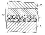
- the conductive pattern 30 includes a conductive particle layer 31 made of metal particles, an electroless plating layer 32 formed on the conductive particle layer 31, and an electroplating layer 33 formed on the electroless plating layer 32. Yes.
- the layer including the conductive particle layer 31 and the electroless plating layer 32 will be described as a first layer, and the electroplating layer 33 will be described as a second layer.
- the conductive particle layer 31 is formed by laminating conductive particles 31A having an average particle diameter of several tens of nm.
- An average particle diameter shows the value (D50) of the integrated value 50% in the integrated distribution of a particle diameter.
- the integrated distribution is created based on a value obtained by performing image analysis of 500 particles with a scanning electron microscope (SEM) and further converting the value of the circle radius of the particles into a volume.
- the thickness of the conductive particle layer 31 is 0.5 ⁇ m or less.
- the conductive particles 31A are made of copper (Cu).
- Cu copper
- particles containing at least one selected from the group of Ag, Au, Pt, Pd, Ru, Sn, Ni, Fe, Co, Ti, and In are used as the conductive particles 31A.
- the conductive particle layer 31 can be formed by a mixture of the conductive particles 31A.
- the particle diameter of the conductive particles 31A is preferably in the range of 30 nm to 100 nm. By setting the particle diameter in such a range, the surface of the conductive particle layer 31 can be smoothed.
- the plurality of conductive particles 31 ⁇ / b> A are connected to each other by sintering or melting at the portion where the adjacent conductive particles 31 ⁇ / b> A contact each other.
- the conductive particles 31A and the conductive substrate 10 are connected to each other by sintering or melting a portion where the conductive particles 31A and the conductive substrate 10 are in contact with each other.
- the electroless plating layer 32 is formed by electroless plating of a metal such as copper, silver or nickel (hereinafter referred to as electroless plating metal).
- electroless plating metal a metal such as copper, silver or nickel
- electroless plating metal When electroconductive particle 31A is a copper particle, it is preferable to form the electroless-plating layer 32 with copper or nickel from a viewpoint of adhesiveness with a copper particle.
- the electroless plating layer 32 includes a lower layer formed in the same layer as the conductive particle layer 31 and an upper layer stacked on the lower layer.
- the lower layer is a layer made of electroless plating metal filled in a gap between the conductive particles 31A.
- the upper layer is a layer containing an electroless plating metal as a main component.
- the thickness of the electroless plating layer 32 is 0.1 ⁇ m to 0.5 ⁇ m.
- the electroplating layer 33 is formed by electroplating a metal such as copper or nickel.
- the thickness of the electroplating layer 33 is 5 ⁇ m to 30 ⁇ m.
- the thickness of the electroplating layer 33 is larger than the thickness of the electroless plating layer 32.
- the thickness of the electroplating layer 33 is set according to the use of the printed wiring board 1.
- a through hole 41 is formed in the insulating layer 20 so as to reach the conductive substrate 10.
- the blind via 40 is formed by sequentially laminating the conductive particle layer 31, the electroless plating layer 32, and the electroplating layer 33 at a position corresponding to the through hole 41.
- the blind via 40 has the same structure as the conductive pattern 30.
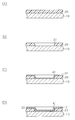
- a solution-like polyimide precursor resin is applied onto a conductive substrate 10 having a thickness of 10 ⁇ m to 500 ⁇ m. Thereafter, the polyimide precursor resin is heated at 300 ° C. or higher to be cured. As a result, the insulating layer 20 having a thickness of 10 ⁇ m to 200 ⁇ m is formed on the conductive substrate 10.
- a through hole 41 having a diameter of 10 ⁇ m to 200 ⁇ m is formed in a portion corresponding to the blind via 40 in the insulating layer 20 (through hole forming step).
- a laser method or an etching method is used to form the through hole 41.
- the through hole 41 is formed until the bottom surface of the through hole 41 reaches the conductive substrate 10, that is, until the depth of the through hole 41 is equal to the thickness of the insulating layer 20.
- the inner diameter of the through hole 41 is 10 ⁇ m to 200 ⁇ m.
- a desmear process is performed to remove resin burrs, resin powder, and the like generated by laser or etching.
- the conductive ink is applied to the entire surface of the conductive substrate 10, and the applied conductive ink is further dried (first layer forming step). .
- the conductive ink is dried, in order to remove the oxide formed on the surface of the conductive particles 31A and the surface of the conductive substrate 10, an oxide remover is applied, and the applied oxide remover is further dried. .
- heat treatment is performed to sinter the conductive particles 31A.
- the surface treatment method for the insulating layer 20 plasma treatment, alkali treatment for hydrophilizing the surface with an alkaline solution, corona treatment for modifying the surface of the object by corona discharge, UV treatment for modifying the surface of the object by ultraviolet rays, etc. Is mentioned.
- the surface of the insulating layer 20 can be roughened, or a hydrophilic group can be introduced into the surface of the insulating layer 20. As a result, the surface tension between the conductive ink and the insulating layer 20 decreases.
- the conductive ink is prepared by dispersing the conductive particles 31A in a predetermined solvent.
- a particle dispersant is used for dispersing the conductive particles 31A.
- water is used as the solvent.
- the viscosity of the conductive ink is almost the same as the viscosity of water. For this reason, even if the diameter of the through hole 41 is as small as 10 ⁇ m, the through hole 41 can be easily filled with the conductive ink.
- the solvent a volatile solvent such as ethanol or a mixed solution of water and a volatile solvent can be used.
- the conductive particles 31A particles having an average particle diameter of several tens of nm are used.
- the particle dispersant for example, a polymer dispersant having a molecular weight of 2000 to 100,000 is used. Specifically, amine-based polymer dispersants such as polyethyleneimine and polyvinylpyrrolidone are used as the particle dispersant. Further, as the particle dispersant, a hydrocarbon-based polymer dispersant having a carboxylic acid group in the molecule such as polyacrylic acid and carboxymethyl cellulose can be used.
- the conductive ink is applied to the entire surface of the conductive substrate 10 using a roller.
- the thickness of the applied conductive ink is adjusted so that the thickness of the conductive ink after drying is 0.1 ⁇ m.
- methods such as spin coating, spray coating, bar coating, die coating, slit coating, and dip coating can be used.
- water in the conductive ink is evaporated, so that a temperature of 80 ° C. is maintained for a predetermined time in an air atmosphere.
- a thin layer of conductive particles 31 ⁇ / b> A is formed on the surface of the insulating layer 20.
- an oxide remover is applied to the surface of the conductive particles 31 ⁇ / b> A and the surface of the conductive substrate 10.
- the oxide removing agent is prepared by dissolving an oxide removing substance in a predetermined solvent.
- a predetermined solvent for example, water is used as the solvent.
- a volatile solvent such as ethanol or a mixed solution of water and a volatile solvent can be used.
- the oxide remover is heated in an inert gas atmosphere after coating.
- the heating temperature of the oxide removing agent is 50 ° C. to 450 ° C., more preferably 100 ° C. to 400 ° C.
- the heat treatment time is 1 minute to 200 minutes, more preferably 10 minutes to 60 minutes.
- oxide removal substances As oxide removal substances, it is classified into the following two types.
- the first type oxide removing substance is a reducing substance that reduces oxide.
- reducing substances include hypophosphorous acid, phosphorous acid, ascorbic acid, ethylenediaminetetraacetic acid (EDTA), alcohol, hydrazine, formaldehyde and the like.
- the second type oxide removing substance is an acidic or alkaline substance that dissolves the oxide.
- Such substances include allylamine, formic acid, glutamic acid, fatty acid, lactic acid, phthalic acid, maleic acid, malic acid, boric acid, ammonium chloride, magnesium chloride, methyl chloride, chloroform, sodium acetate, potassium bromide, calcium bromide, Examples include trichloroethylene, sodium sulfide, sodium iodide, aluminum sulfate, hexachloroethane, and the like.
- allylamine, formic acid, glutamic acid, fatty acid, lactic acid, phthalic acid, maleic acid, and malic acid are suitable because ionic elements do not remain even if they remain after drying of the oxide remover.
- the oxide removing agent is used by dissolving one or both of the first type oxide removing material and the second type oxide removing material in a solvent. Moreover, you may add the dispersing agent of an oxide removal substance, and the pH adjuster which adjusts the pH of a solution in a solvent.
- the conductive particles 31A are sintered and organic substances other than the conductive particles 31A (hereinafter referred to as “residual organic substances”) are removed.
- the residual organic material include a particle dispersant and an oxide remover contained in the conductive ink.
- the heat treatment is performed, for example, in a nitrogen gas atmosphere in order to suppress oxidation of the conductive particles 31A.
- the temperature is raised to 350 ° C. at a rate of 5 ° C./min, and the temperature of 350 ° C. is maintained for 30 minutes.
- the conductive particle 31A is formed by sintering the conductive particles 31A and connecting the conductive particles 31A to each other.
- the reason why sintering can be performed at a relatively low temperature is that the surface energy of the conductive particles 31A having an average particle diameter of several tens of nanometers is high.
- the electroless plating layer 32 is formed so that the thickness from the insulating layer 20 is about 0.2 ⁇ m. Specifically, after a catalytic metal such as Pd—Sn is applied on the conductive particle layer 31 and the insulating layer 20, Sn is dissolved and Pd is attached to the conductive particle layer 31. Then, the electroless plating layer 32 is formed on the conductive particle layer 31 and the insulating layer 20 by being immersed in a copper plating solution. Thus, the gap between the adjacent conductive particles 31A and the gap between the conductive particles 31A and the conductive substrate 10 are filled with the electroless plating metal. As a result, the density of the conductive particle layer 31 increases, and a dense electroless plating layer 32 is formed on the surface of the conductive particle layer 31.
- a catalytic metal such as Pd—Sn
- the conductive pattern 30 and the blind via 40 are formed by a semi-additive pattern method. Hereinafter, each process is demonstrated concretely.
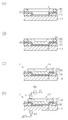
- a resist 50 is formed on the surface of the electroless plating layer 32 excluding portions corresponding to the blind vias 40 and the conductive patterns 30.
- the resist 50 is formed by laminating a photoresist on a substrate and then exposing and developing using a photomask.
- electroplating of copper is performed to form an electroplating layer 33 on the electroless plating layer 32 (second layer forming step).
- the conductive pattern 30 and the blind via 40 are formed on the conductive particle layer 31 and the insulating layer 20.
- the seed layer that is, the electroless plating layer 32 and the conductive particle layer 31 are removed with perhydrosulfuric acid. Furthermore, Pd adhering to the insulating layer 20 during electroless plating is removed.
- the blind via 40 and the conductive pattern 30 are formed by the above steps (pattern layer forming step).
- the present invention is characterized by the steps shown in FIGS. 4 (A) to 4 (C). That is, unlike the conventional method of manufacturing the blind via 40, the step of filling the through hole 41 with a conductive material, that is, the application of the conductive ink is performed before electroplating, so the low viscosity conductive ink is used. be able to. Furthermore, since it is only necessary to remove the seed layer (electroless plating layer 32 and conductive particle layer 31) after applying the conductive ink, it is possible to suppress the variation in the size of the blind via 40. Therefore, the dimensional accuracy of the blind via 40 can be made the same as the pattern accuracy of the semi-additive pattern method.
- the heating treatment for the blind via 40 is performed in order to reduce the resistance value of the blind via 40.
- this process will be described.
- the probe 61 on the high potential side of the constant current source 60 is brought into contact with the electroplating layer 33 of the blind via 40. Further, the ground-side probe 62 is brought into contact with the conductive substrate 10. Then, a constant current is passed through the blind via 40 using both probes 61 and 62.
- the resistance of the conductive particle layer 31 and the electroless plating layer 32 includes the conductivity of the conductive particles 31A, the conductivity of the electroless plating, the contact resistance between the conductive particles 31A, and the contact resistance between the conductive particles 31A and the conductive substrate 10. It is determined by the contact resistance between the electroless plating and the conductive particles 31A.
- the resistances of the conductive particle layer 31 and the electroless plating layer 32 are particularly greatly affected by the contact resistance between the conductive particles 31 ⁇ / b> A and the contact resistance between the conductive particles 31 ⁇ / b> A and the conductive substrate 10.
- the contact resistances contribute more greatly to the resistance of the conductive particle layer 31 and the electroless plating layer 32. become. Therefore, in order to reduce each contact resistance, a contact current between the conductive particles 31A and a contact portion between the conductive particles 31A and the conductive substrate 10 are sintered or melted by flowing a pulse current through the blind via 40, respectively. To do. Thereby, the conductive particles 31A are connected to each other, and the conductive particles 31A and the conductive substrate 10 are connected to each other. In this case, the contact resistance between the conductive particles 31A and the contact resistance between the conductive particles 31A and the conductive substrate 10 are reduced.
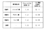
- Example 1 energization heating was performed after the oxide remover was applied. In the comparative example, energization heating was performed without applying the oxide remover. And about each Example and the comparative example, the resistance value of the blind via 40 before and behind energization heating was measured, respectively.
- the conductive substrate 10 on which the insulating layer 20 was laminated was used.
- a SUS304 substrate having a thickness of 20 ⁇ m was used.
- the insulating layer 20 was formed from a polyimide resin.
- the thickness of the insulating layer 20 was 10 ⁇ m.
- the YAG laser was irradiated to the insulating layer 20 to form the through hole 41 of the blind via 40.
- the diameter of the through hole 41 was 60 ⁇ m.
- the conductive ink an aqueous solution in which copper particles having an average particle diameter of 40 nm were dispersed in water by 8% by mass was used.
- FIG. After applying conductive ink to a base material, it heated at 80 degreeC for about 30 second, and dried the conductive substrate 10.
- a 1.0% by mass aqueous solution of ascorbic acid as an oxide removing agent (reducing agent) was applied on the dried conductive ink. Thereafter, a temperature of 90 ° C. was maintained for 30 minutes in an inert gas atmosphere. Subsequently, the temperature was increased to 350 ° C. at a rate of 5 ° C./min, and further heated at a temperature of 350 ° C. for 30 minutes to form the conductive particle layer 31.
- -Copper electroless plating was performed on the conductive particle layer 31. The thickness of the electroless plating layer was 0.2 ⁇ m.
- the conductive pattern 30 and the blind via 40 were formed on the electroless plating layer by a semi-additive pattern method.
- a pulse current having a current of 5 A and a pulse width of 100 ⁇ s was applied to the blind via 40. (result) -The resistance value of the blind via 40 before energization was 1.4 ⁇ . The resistance value of the blind via 40 after energization was 0.11 ⁇ .
- Example 2 The same production conditions as in Example 1 except that after the conductive ink was dried, a 1.0% by mass aqueous solution of glutamic acid was applied as an oxide remover (oxide solubilizer) onto the dried conductive ink. did. (result) -The resistance value of the blind via 40 before energization was 1.2 ⁇ . -The resistance value of the blind via 40 after energization was 0.09 ⁇ .
- Example 3 The same production conditions as in Example 1 except that after drying the conductive ink, a 1.0% by weight aqueous solution of maleic acid as an oxide remover (oxide solubilizer) was applied on the dried product of the conductive ink. It was. (result) -The resistance value of the blind via 40 before energization was 1.2 ⁇ . -The resistance value of the blind via 40 after energization was 0.09 ⁇ .
- pulse energization was performed on the blind via 40, but the effect of pulse energization was the same. That is, the resistance value after energization was smaller than the resistance value before energization. This is because the resistance value between the contact portion between the conductive particles 31A and the contact portion between the conductive particles 31A and the conductive substrate 10 was relatively high before the pulse energization. It is considered that the resistance value of each contact portion was lowered by heating or melting or sintering.
- the resistance value of the blind via 40 before energization was compared, the resistance value of each example was smaller than the resistance value of the comparative example. This is considered to be because the oxide removing agent was applied in all the examples, and the oxide on the surface of the conductive particles 31A and the oxide on the surface of the conductive substrate 10 (bottom surface of the blind via 40) were removed.
- Conductive ink is applied to the insulating layer 20 to form the conductive particle layer 31.
- the blind via 40 is formed on the conductive particle layer 31 by electroplating. Further, the conductive particle layer 31 and the electroless plating layer 32 around the blind via 40 are removed. According to this method, the conductive particle layer 31 is removed after the blind via 40 is formed. For this reason, a conductive ink having a low viscosity can be used for forming the conductive particle layer 31. Therefore, it is possible to suppress the variation of the blind via diameter due to the low viscosity of the conductive ink.
- the blind via 40 includes a conductive particle layer 31. Further, the resistance value of the conductive particle layer 31 is easily influenced by the contact resistance at the contact portion between the conductive particles 31A. According to this embodiment, the contact portion between the conductive particles 31 ⁇ / b> A is melted or sintered by performing the energization heating process of the blind via 40. Thereby, the contact resistance between the conductive particles 31 ⁇ / b> A and the resistance value of the blind via 40 can be lowered.
- the electroless plating layer 32 is formed on the conductive particle layer 31. According to this method, since the plating material is filled in the gaps between the conductive particles 31A, the conductive particle layer 31 can be made dense. As a result, the resistance value of the blind via 40 can be lowered.
- an oxide removing agent is applied on the conductive particle layer 31.
- the oxide removing agent removes the oxide on the surface of the conductive substrate 10, thereby increasing the adhesive strength between the conductive substrate 10 and the conductive particle layer 31. As a result, peeling between the conductive substrate 10 and the conductive particle layer 31 is suppressed.
- the oxide remover is heat-treated in an inert atmosphere after coating. According to this method, compared with the heat treatment in air, the reaction between the oxide remover and oxygen in the air is suppressed, and the reaction between the oxide remover and the oxide of the conductive substrate 10 is promoted. . Therefore, peeling between the conductive substrate 10 and the conductive particle layer 31 is further suppressed.
- the oxide removing agent at least one of a reducing agent that reduces the oxide and a dissolved substance that dissolves the oxide is used.
- the reducing agent reduces the oxide and decomposes the oxide.
- the dissolved material dissolves the oxide and decomposes the oxide.
- the blind via 40 includes the conductive particle layer 31, the electroless plating layer 32, And an electroplating layer 33.
- the blind via 40 is formed by sequentially laminating an electroless plating and electroplating layer 33 on the insulating layer 20.
- the electroless plating layer 32 may be peeled off from the insulating layer 20.
- the electroplating layer 33 is connected to the conductive substrate 10 via the conductive particle layer 31 and the electroless plating layer 32.
- the adhesive strength between the conductive particle layer 31 and the insulating layer 20 is greater than the adhesive strength between the electroless plating and the insulating layer 20. For this reason, peeling of the conductive particle layer 31 from the insulating layer 20 is suppressed.
- the plurality of conductive particles 31A are connected to each other by being melted or sintered at the portions in contact with each other.
- the conductive particles 31A and the conductive substrate 10 are melted or sintered at a portion in contact with each other and connected to each other. According to this configuration, since the current density of the conduction path of the blind via 40 increases, the resistance value of the blind via 40 can be reduced.
- the connection strength between the stainless steel substrate and the blind via 40 may be reduced.
- the stainless steel substrate as the conductive substrate 10 may have a nickel layer on the contact surface with the insulating layer 20. According to this configuration, since the oxidation of the surface of the stainless steel is suppressed by the nickel layer, it is possible to suppress a decrease in the connection strength between the stainless steel substrate and the blind via 40.
- the oxide removing agent is applied to the conductive particle layer 31.
- the oxide removing agent may be added to the conductive ink in advance. Even in this way, the oxide of the conductive substrate 10 can be decomposed by bringing the reducing agent and dissolved substance in the conductive ink into contact with the oxide of the conductive substrate 10. According to this method, the steps for applying the oxide remover and drying the solution containing the oxide remover are not required, and the manufacturing process is simplified.
- the oxide removing agent was applied and dried, but the drying of the oxide removing agent may be included in the sintering step of the conductive particles 31A.
- the oxide remover coating is heated in an inert atmosphere at two stages of heating temperature. The temperature of the first stage is maintained at a temperature for evaporating the moisture of the oxide removing agent, that is, 50 ° C. to 100 ° C. for 30 minutes. Thereafter, the second stage temperature is set to 350 ° C. and maintained for 30 minutes.
- the conductive pattern 30 and the blind via 40 may be formed by a semi-additive panel method.
- the conductive particle layer 31 and the electroless plating layer 32 can be removed after the conductive pattern 30 is formed, the dimensional accuracy of the blind via 40 can be increased as compared with the conventional manufacturing method.
- the present invention may be applied to the blind via 40 that connects the conductive pattern 30 and the conductive pattern 30 disposed above or below the conductive pattern 30.
- the present invention may be applied to various printed wiring boards 1 in addition to the printed wiring board 1 for the magnetic head suspension for mounting the magnetic head in the hard disk drive.
Landscapes
- Engineering & Computer Science (AREA)
- Manufacturing & Machinery (AREA)
- Microelectronics & Electronic Packaging (AREA)
- Printing Elements For Providing Electric Connections Between Printed Circuits (AREA)
- Adjustment Of The Magnetic Head Position Track Following On Tapes (AREA)
- Supporting Of Heads In Record-Carrier Devices (AREA)
- Insulated Metal Substrates For Printed Circuits (AREA)
- Manufacturing Of Printed Wiring (AREA)
- Chemically Coating (AREA)
Abstract
Description
・母材には、絶縁層20が積層された導電基板10を用いた。
・導電基板10には、厚さ20μmであるSUS304の基板を用いた。
・絶縁層20をポリイミド樹脂により形成した。絶縁層20の厚さを10μmとした。
・絶縁層20にYAGレーザを照射して、ブラインドビア40の貫通孔41を形成した。貫通孔41の直径を60μmとした。
・導電性インクには、平均粒径が40nmである銅粒子を8質量%だけ水に分散させた水溶液を用いた。
・導電性インクを母材に塗布した後、80℃で約30秒間加熱し、導電基板10を乾燥した。
・導電性インクの乾燥後、酸化物除去剤(還元剤)としてのアスコルビン酸の1.0質量%水溶液を、導電性インクの乾燥物上に塗布した。この後、不活性ガス雰囲気下で90℃の温度を30分間維持した。続いて、5℃/分の昇温速度で350℃にまで昇温し、更に温度350℃で30分間加熱して、導電粒子層31を形成した。
・導電粒子層31上に、銅の無電解めっきを行った。無電解めっき層の厚みを0.2μmとした。
・無電解めっき層上に、セミアディティブ-パターン法により導電パターン30およびブラインドビア40を形成した。
・電流5A、パルス幅100μsのパルス電流を、ブラインドビア40に通電した。
(結果)
・ブラインドビア40の通電前の抵抗値は1.4Ωであった。
・ブラインドビア40の通電後の抵抗値は0.11Ωであった。
・導電性インクの乾燥後、酸化物除去剤(酸化物溶解剤)として、グルタミン酸の1.0質量%水溶液を導電性インクの乾燥物上に塗布した以外は、実施例1と同じ製造条件とした。
(結果)
・ブラインドビア40の通電前の抵抗値は1.2Ωであった。
・ブラインドビア40の通電後の抵抗値は0.09Ωであった。
・導電性インクの乾燥後、酸化物除去剤(酸化物溶解剤)としてのマレイン酸の1.0質量%水溶液を導電性インクの乾燥物上に塗布した以外は、実施例1と同じ製造条件とした。
(結果)
・ブラインドビア40の通電前の抵抗値は1.2Ωであった。
・ブラインドビア40の通電後の抵抗値は0.09Ωであった。
・酸化物除去剤を塗布しなかったこと以外は、実施例1~3と同じ製造条件とした。
(結果)
・ブラインドビア40の通電前の抵抗値は1.8Ωであった。
・ブラインドビア40の通電後の抵抗値は0.14Ωであった。
図5を参照して、各実施例および比較例を比較する。
(8)ブラインドビア40は、導電粒子層31、無電解めっき層32、及び電気めっき層33を備えている。ブラインドビア40は、絶縁層20上に無電解めっき及び電気めっき層33を順に積層して形成されている。しかしながら、この構造では、絶縁層20及び無電解めっき層32間の接着強度が弱いため、無電解めっき層32が絶縁層20から剥離する虞がある。この点、本実施形態によれば、電気めっき層33は、導電粒子層31および無電解めっき層32を介して導電基板10に接続されている。この場合、導電粒子層31と絶縁層20との接着力は、無電解めっきと絶縁層20との接着強度よりも大きい。このため、絶縁層20からの導電粒子層31の剥離が抑制される。
Claims (12)
- 絶縁層、前記絶縁層の第1の面に形成された第1導電層、前記絶縁層の第2の面に形成された第2導電層、及び前記第1導電層と前記第2導電層とを接続するブラインドビアを備えたプリント配線板の製造方法において、
前記絶縁層において、前記第1導電層に達するように貫通孔を形成する貫通孔形成工程と、
前記貫通孔を含む領域に、導電性粒子を含む導電性インクを塗布して導電粒子層を形成する第1層形成工程と、
電気めっきにより、前記導電粒子層上に電気めっき層を形成する第2層形成工程と、
前記貫通孔周囲の前記導電粒子層を除去し、前記導電粒子層及び前記電気めっき層を含む前記第2導電層を形成するパターン層形成工程と
を含むことを特徴とするプリント配線板の製造方法。 - 請求項1に記載のプリント配線板の製造方法において、
前記ブラインドビアを形成した後、前記ブラインドビアの通電加熱処理を行うことを特徴とするプリント配線板の製造方法。 - 請求項1又は2に記載のプリント配線板の製造方法において、
前記第1層形成工程は、
前記導電性インクを塗布する工程と、
前記導電性インクの溶媒を蒸発させて前記導電粒子層を形成する工程と、
前記導電粒子層に対して無電解めっき層を形成する工程と
を含むことを特徴とするプリント配線板の製造方法。 - 請求項3に記載のプリント配線板の製造方法において、
前記第1層形成工程は、更に、無電解めっき層を形成する前に、前記第1導電層の表面の酸化物を除去する酸化物除去剤を前記導電粒子層上に塗布する工程を含むことを特徴とするプリント配線板の製造方法。 - 請求項4に記載のプリント配線板の製造方法において、
前記第1層形成工程は、更に、前記酸化物除去剤の塗布後に、不活性雰囲気中で前記酸化物除去剤を加熱処理する工程を含むことを特徴とするプリント配線板の製造方法。 - 請求項4又は5に記載のプリント配線板の製造方法において、
前記酸化物除去剤は、前記酸化物を還元する還元剤、および前記酸化物を溶解する溶解物質の少なくとも一方を含むことを特徴とするプリント配線板の製造方法。 - 請求項6に記載のプリント配線板の製造方法において、
前記還元剤は前記第1導電層の表面の酸化物を還元し、前記溶解物質は前記酸化物を溶解することを特徴とするプリント配線板の製造方法。 - 請求項1~7のいずれか一項に記載のプリント配線板の製造方法において、
前記第1導電層は、ステンレス基板であることを特徴とするプリント配線板の製造方法。 - 請求項8に記載のプリント配線板の製造方法において、
前記ステンレス基板は、前記絶縁層との接触面にニッケル層を有していることを特徴とするプリント配線板の製造方法。 - 絶縁層、前記絶縁層の第1の面に形成された第1導電層、前記絶縁層の第2の面に形成された第2導電層、及び前記第1導電層と前記第2導電層とを接続するブラインドビアとを備えたプリント配線板において、
前記第2導電層は、
前記絶縁層上に形成されかつ複数の導電性粒子を含む導電粒子層と、
前記導電粒子層上に積層された無電解めっき層と、
前記無電解めっき層上に積層された電気めっき層とを備え、
前記ブラインドビアは、
前記絶縁層を貫通する貫通孔と対応する位置に形成されると共に複数の導電性粒子を含む導電粒子層と、
前記ブラインドビアの導電粒子層上に積層された無電解めっき層と、
前記ブラインドビアの無電解めっき層上に積層された電気めっき層とを備え、
前記ブラインドビアは、前記貫通孔の底面で前記第1導電層に接続されていることを特徴とするプリント配線板。 - 請求項10に記載のプリント配線板において、
前記複数の導電性粒子は、互いに接触する部分で溶融又は焼結されて相互に接続され、
前記導電性粒子及び前記第1導電層は、互いに接触する部分で溶融又は焼結されて相互に接続されていることを特徴とするプリント配線板。 - 請求項10又は11に記載のプリント配線板において、
前記貫通孔の直径は10μm以上であり、前記導電粒子層の厚さは0.5μm以下であることを特徴とするプリント配線板。
Priority Applications (1)
| Application Number | Priority Date | Filing Date | Title |
|---|---|---|---|
| CN201280001484.0A CN102918937B (zh) | 2011-04-05 | 2012-03-29 | 印刷电路板以及该印刷电路板的制造方法 |
Applications Claiming Priority (2)
| Application Number | Priority Date | Filing Date | Title |
|---|---|---|---|
| JP2011083902A JP5335023B2 (ja) | 2011-04-05 | 2011-04-05 | プリント配線板の製造方法 |
| JP2011-083902 | 2011-04-05 |
Publications (1)
| Publication Number | Publication Date |
|---|---|
| WO2012137669A1 true WO2012137669A1 (ja) | 2012-10-11 |
Family
ID=46969070
Family Applications (1)
| Application Number | Title | Priority Date | Filing Date |
|---|---|---|---|
| PCT/JP2012/058409 Ceased WO2012137669A1 (ja) | 2011-04-05 | 2012-03-29 | プリント配線板およびそのプリント配線板の製造方法 |
Country Status (3)
| Country | Link |
|---|---|
| JP (1) | JP5335023B2 (ja) |
| CN (1) | CN102918937B (ja) |
| WO (1) | WO2012137669A1 (ja) |
Cited By (1)
| Publication number | Priority date | Publication date | Assignee | Title |
|---|---|---|---|---|
| US12610459B2 (en) | 2020-08-07 | 2026-04-21 | Nitto Denko Corporation | Method for producing wiring circuit board and wiring circuit board |
Families Citing this family (5)
| Publication number | Priority date | Publication date | Assignee | Title |
|---|---|---|---|---|
| CN104347533B (zh) * | 2013-08-01 | 2020-05-26 | 日月光半导体制造股份有限公司 | 半导体封装件及其制造方法 |
| JP6473018B2 (ja) * | 2015-03-10 | 2019-02-20 | 住友電工プリントサーキット株式会社 | プリント配線板用基材の製造方法、プリント配線板用基材及びプリント配線板 |
| CN107634012B (zh) * | 2017-09-13 | 2021-05-07 | 京东方科技集团股份有限公司 | 一种封装基板及其制备方法、显示面板、显示装置 |
| JP7289602B2 (ja) * | 2020-11-13 | 2023-06-12 | 日東電工株式会社 | 配線回路基板、および配線回路基板の製造方法 |
| JP2023031643A (ja) * | 2021-08-25 | 2023-03-09 | アオイ電子株式会社 | 配線基板およびその製造方法 |
Citations (2)
| Publication number | Priority date | Publication date | Assignee | Title |
|---|---|---|---|---|
| JP2010118460A (ja) * | 2008-11-12 | 2010-05-27 | Sumitomo Electric Ind Ltd | プリント配線板およびその製造方法 |
| JP2010272837A (ja) * | 2009-04-24 | 2010-12-02 | Sumitomo Electric Ind Ltd | プリント配線板用基板、プリント配線板、及びプリント配線板用基板の製造方法 |
Family Cites Families (4)
| Publication number | Priority date | Publication date | Assignee | Title |
|---|---|---|---|---|
| JP2006179822A (ja) * | 2004-12-24 | 2006-07-06 | Cmk Corp | プリント配線板とその製造方法 |
| JP2009026898A (ja) * | 2007-07-18 | 2009-02-05 | Daisho Denshi:Kk | 多層プリント配線板の製造方法、多層プリント配線板 |
| JP2010153628A (ja) * | 2008-12-25 | 2010-07-08 | Hitachi Chem Co Ltd | 多層配線基板の製造方法 |
| KR20120003458A (ko) * | 2009-04-24 | 2012-01-10 | 스미토모 덴키 고교 가부시키가이샤 | 프린트 배선판용 기판, 프린트 배선판, 및 그들의 제조방법 |
-
2011
- 2011-04-05 JP JP2011083902A patent/JP5335023B2/ja active Active
-
2012
- 2012-03-29 WO PCT/JP2012/058409 patent/WO2012137669A1/ja not_active Ceased
- 2012-03-29 CN CN201280001484.0A patent/CN102918937B/zh not_active Expired - Fee Related
Patent Citations (2)
| Publication number | Priority date | Publication date | Assignee | Title |
|---|---|---|---|---|
| JP2010118460A (ja) * | 2008-11-12 | 2010-05-27 | Sumitomo Electric Ind Ltd | プリント配線板およびその製造方法 |
| JP2010272837A (ja) * | 2009-04-24 | 2010-12-02 | Sumitomo Electric Ind Ltd | プリント配線板用基板、プリント配線板、及びプリント配線板用基板の製造方法 |
Cited By (1)
| Publication number | Priority date | Publication date | Assignee | Title |
|---|---|---|---|---|
| US12610459B2 (en) | 2020-08-07 | 2026-04-21 | Nitto Denko Corporation | Method for producing wiring circuit board and wiring circuit board |
Also Published As
| Publication number | Publication date |
|---|---|
| JP2012222047A (ja) | 2012-11-12 |
| CN102918937B (zh) | 2016-11-09 |
| JP5335023B2 (ja) | 2013-11-06 |
| CN102918937A (zh) | 2013-02-06 |
Similar Documents
| Publication | Publication Date | Title |
|---|---|---|
| JP4741616B2 (ja) | フォトレジスト積層基板の形成方法 | |
| JP5335023B2 (ja) | プリント配線板の製造方法 | |
| US8138422B2 (en) | Printed circuit board with conductive ink/paste, having plating layers, and method for manufacturing the same | |
| EP2424337A1 (en) | Substrate for printed wiring board, printed wiring board, and methods for producing same | |
| JP2010272837A (ja) | プリント配線板用基板、プリント配線板、及びプリント配線板用基板の製造方法 | |
| CN107113981B (zh) | 印刷线路板用基板以及印刷线路板用基板的制造方法 | |
| JP6400503B2 (ja) | プリント配線板用基材及びプリント配線板 | |
| JP6484218B2 (ja) | プリント配線板用基板及びプリント配線板 | |
| JP2012114152A (ja) | プリント配線板用基板およびプリント配線板ならびにプリント配線板用基板の製造方法 | |
| JPWO2016117575A1 (ja) | プリント配線板用基材、プリント配線板及びプリント配線板の製造方法 | |
| JP5711788B2 (ja) | プリント配線板 | |
| CN106688314A (zh) | 印刷线路板用基材、印刷线路板以及印刷线路板用基材的制造方法 | |
| JP6466110B2 (ja) | プリント配線板用基板、プリント配線板及びプリント配線板用基板の製造方法 | |
| JP6484026B2 (ja) | プリント配線板用基板及びプリント配線板並びにプリント配線板用基板の製造方法 | |
| JPWO2016194972A1 (ja) | プリント配線板用原板及びプリント配線板、並びにプリント配線板用原板の製造方法 | |
| JP2014041969A (ja) | プリント配線板の製造方法 | |
| JP2010062525A (ja) | 印刷回路基板及びその製造方法 | |
| JP4775204B2 (ja) | 導電性パターンの形成方法、配線板の製造方法及び配線板 | |
| JP2013093359A (ja) | 半導体チップ搭載用基板及びその製造方法 | |
| JP7032127B2 (ja) | プリント配線板用基材、プリント配線板及びプリント配線板用基材の製造方法 | |
| JP2019161016A (ja) | プリント配線板用基板、プリント配線板、プリント配線板用基板の製造方法及び銅ナノインク | |
| US9967976B2 (en) | Substrate for printed circuit board, printed circuit board, and method for producing substrate for printed circuit board | |
| JP2010118460A (ja) | プリント配線板およびその製造方法 | |
| JP5327107B2 (ja) | プリント配線板用基板、プリント配線板、プリント配線板の製造方法 | |
| JP2010056499A (ja) | 多層配線基板の製造方法及び多層配線基板 |
Legal Events
| Date | Code | Title | Description |
|---|---|---|---|
| WWE | Wipo information: entry into national phase |
Ref document number: 201280001484.0 Country of ref document: CN |
|
| 121 | Ep: the epo has been informed by wipo that ep was designated in this application |
Ref document number: 12767599 Country of ref document: EP Kind code of ref document: A1 |
|
| WWE | Wipo information: entry into national phase |
Ref document number: 1201006189 Country of ref document: TH |
|
| NENP | Non-entry into the national phase |
Ref country code: DE |
|
| 122 | Ep: pct application non-entry in european phase |
Ref document number: 12767599 Country of ref document: EP Kind code of ref document: A1 |