WO2012133891A1 - 現像方法、配線パターンの形成方法、及びアクティブマトリクス基板の製造方法 - Google Patents
現像方法、配線パターンの形成方法、及びアクティブマトリクス基板の製造方法 Download PDFInfo
- Publication number
- WO2012133891A1 WO2012133891A1 PCT/JP2012/058909 JP2012058909W WO2012133891A1 WO 2012133891 A1 WO2012133891 A1 WO 2012133891A1 JP 2012058909 W JP2012058909 W JP 2012058909W WO 2012133891 A1 WO2012133891 A1 WO 2012133891A1
- Authority
- WO
- WIPO (PCT)
- Prior art keywords
- substrate
- developer
- microcapsule
- developing
- development
- Prior art date
- Legal status (The legal status is an assumption and is not a legal conclusion. Google has not performed a legal analysis and makes no representation as to the accuracy of the status listed.)
- Ceased
Links
Images







Classifications
-
- G—PHYSICS
- G03—PHOTOGRAPHY; CINEMATOGRAPHY; ANALOGOUS TECHNIQUES USING WAVES OTHER THAN OPTICAL WAVES; ELECTROGRAPHY; HOLOGRAPHY
- G03F—PHOTOMECHANICAL PRODUCTION OF TEXTURED OR PATTERNED SURFACES, e.g. FOR PRINTING, FOR PROCESSING OF SEMICONDUCTOR DEVICES; MATERIALS THEREFOR; ORIGINALS THEREFOR; APPARATUS SPECIALLY ADAPTED THEREFOR
- G03F7/00—Photomechanical, e.g. photolithographic, production of textured or patterned surfaces, e.g. printing surfaces; Materials therefor, e.g. comprising photoresists; Apparatus specially adapted therefor
- G03F7/26—Processing photosensitive materials; Apparatus therefor
- G03F7/30—Imagewise removal using liquid means
Definitions
- the present invention relates to a developing method, a method for forming a wiring pattern, and a method for manufacturing an active matrix substrate.
- an active matrix substrate constituting a liquid crystal panel is manufactured by repeating exposure, development, and etching processes a plurality of times using photolithography technology.
- a so-called paddle method is known in which development is performed only with a developer once applied on the substrate.
- the degree of reduction in the development rate differs depending on the difference in resist pattern density on the substrate, the difference in the amount of developer applied, and the like, and the degree of development on the substrate may vary.
- Patent Document 1 discloses a developing method that can reduce the variation in the degree of development on the substrate.
- An object of this invention is to provide the image development method which can reduce the usage-amount of a developing solution.
- a composite developer in which microcapsules including a second developer are dispersed in a first developer is applied onto a substrate on which a resist pattern after exposure is formed.
- a first development step of developing a part of the resist pattern using the first developer in the composite developer and after the first development step, the micro development A destruction step of breaking the capsule and causing the second developer to flow out of the microcapsule; and after the breaking step, using the second developer that has flowed out of the microcapsule, And a second developing step for developing the remaining part.
- the developing rate by the developing solution is lowered by developing a part of the resist pattern, the remaining undeveloped portion at a high developing rate again by the new developing solution that has flowed out from the destroyed microcapsules. Can be developed. For this reason, it is not necessary to apply a new developer onto the substrate again at the timing when the development rate is lowered, and the amount of developer used can be reduced. Furthermore, development can be performed again at a high development rate with a new developer flowing out of the microcapsule, so that development can be completed in all areas where the developer on the substrate is applied, and the degree of development on the substrate Variation can be prevented or suppressed.
- the composite developer is applied in order from the front side of the traveling direction along the traveling direction of the substrate.
- the composite developer may be coated on a substrate on which the resist pattern having a dense portion having a high pattern density and a sparse portion having a low pattern density is formed.
- the dense portion with high pattern density and the sparse portion with low pattern density differ in the amount of dissolution of the resist by the developer. Therefore, the degree of decrease in the development rate differs between the dense portion and the sparse portion.
- the variation in the degree of reduction in the development rate between the dense part and the sparse part is varied. Can be prevented or suppressed.
- the composite developer may be coated on the entire surface of the substrate. According to this developing method, the amount of developer used can be reduced over the entire surface of the substrate.
- the microcapsule is a microcapsule that can be broken by ultrasonic vibration energy, and in the breaking step, the ultrasonic vibration energy is externally applied to the microcapsule to vibrate the microcapsule at a resonance frequency. Thus, the microcapsules may be destroyed. According to this developing method, a specific configuration for breaking the microcapsules can be realized in the breaking step, and the microcapsules can be broken from the outside.
- the ultrasonic vibration energy of 20 kHz or more may be applied to the microcapsule. According to this developing method, a specific configuration for breaking the microcapsules with ultrasonic vibration energy can be realized in the breaking step.
- the microcapsule is a microcapsule that can be broken by laser light, and in the breaking step, the microcapsule may be broken by irradiating the microcapsule from the outside. According to this developing method, a specific configuration for breaking the microcapsules can be realized in the breaking step, and the microcapsules can be broken from the outside.
- the microcapsule may be irradiated with a YAG laser as a laser beam.
- an excimer laser may be irradiated as laser light to the microcapsules. According to these developing methods, it is possible to realize a specific configuration for destroying the microcapsules with laser light in the destruction step.
- a removal step of removing the first developer and the second developer from the substrate may be further provided. According to this developing method, it is possible to obtain a clean substrate from which the developer is removed after development.
- 2nd aspect of this invention is related with the formation method of the wiring pattern which forms a wiring pattern using one of said developing methods.
- the wiring pattern can be formed on the substrate while reducing the amount of the developer used.
- a method of manufacturing an active matrix substrate including the substrate and a thin film transistor formed on the substrate, wherein the wiring pattern is formed by the above-described wiring pattern forming method.
- the present invention relates to a method for manufacturing an active matrix substrate.
- a thin film transistor can be formed with a wiring pattern formed while reducing the amount of developer used, and therefore an active matrix substrate excellent in productivity and the like can be manufactured.
- the image development method which can reduce the usage-amount of a developing solution can be provided.
- FIG. 1 is a cross-sectional view of a liquid crystal display device 10 according to Embodiment 1.
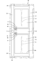
- FIG. A cross-sectional view of the liquid crystal panel 11 is shown.
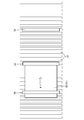
- the top view which expanded a part of active matrix substrate 30 is shown.
- FIG. 2 is a side view of a developing method and a wiring pattern forming method according to Embodiment 1 in which a developer is applied on a substrate on which a resist pattern after exposure is formed.
- the figure which expanded a part of composite developing solution 70 is shown.
- substrate with which the resist pattern after exposure was formed is shown.
- substrate with which the resist pattern after exposure was formed is shown.
- the side view of the process of destroying the microcapsule 80 in the composite developing solution 70 is shown.
- the figure which expanded a part of composite developing solution 70 at the time of destruction of the microcapsule 80 is shown.
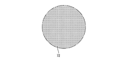
- the figure which expanded a part of composite developing solution 72 is shown.
- the side view of the process of removing a developing solution is shown.
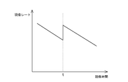
- the graph showing the relationship between development time and a development rate is shown.
- FIG. 1 is a cross-sectional view of a liquid crystal display device 10 according to the first embodiment.
- the upper side shown in FIG. 1 is the front side, and the lower side is the back side.
- the liquid crystal display device 10 includes a liquid crystal panel 11 as a display panel and a backlight device 12 as an external light source, and these are integrally held by a bezel 13 or the like having a frame shape. It is like that.
- the backlight device 12 is a so-called direct-type backlight in which a light source is arranged directly under the back surface of the liquid crystal panel 11, and includes a chassis 14 having a light output portion on the front side (light emission side, liquid crystal panel 11 side), 14, a reflection sheet 15 laid in the optical member 14, an optical member 16 attached so as to cover the light output portion of the chassis, a frame 17 for fixing the optical member 16, and a plurality of pieces accommodated in parallel in the chassis 14.
- the cold-cathode tube 18 is configured to have a lamp holder 19 that shields light from an end portion of the cold-cathode tube 18 and has light reflectivity.
- FIG. 2 shows a cross-sectional view of the liquid crystal panel 11.
- the liquid crystal panel 11 includes a liquid crystal material, which is a substance whose optical characteristics change with application of an electric field, between a pair of transparent (translucent) glass substrates 20 and 30. A liquid crystal layer 29 is enclosed.
- the two substrates 20 and 30 constituting the liquid crystal panel 11 the one disposed on the back side (backlight device 12 side) is the active matrix substrate 30, and the one disposed on the front side (light emitting side) is the CF substrate 20. It is said that.
- FIG. 1 shows a cross-sectional view of the liquid crystal panel 11.
- TFTs Thin Film Transistors
- pixel electrodes 36 which are switching elements. Many are arranged side by side.
- alignment films 25 and 35 are formed on the inner surfaces of both the substrates 20 and 30 to face the liquid crystal layer 29 and align liquid crystal molecules contained in the liquid crystal layer 29, respectively.
- the pretilt angle of the liquid crystal molecules in the liquid crystal layer 29 is controlled by irradiating the alignment films 25 and 35 with ultraviolet rays.
- a polarizing plate 22 that is integrated with the front and back surfaces is attached to the outer surface sides of the substrates 20 and 30.
- the configuration of the CF substrate 20 will be described.
- a plurality of the colored portions 21 are arranged in parallel in a matrix at positions that overlap each pixel electrode 36 on the active matrix substrate 20 side, which will be described later, in plan view.
- the light-shielding part (black matrix) 23 which makes
- the light shielding portion 23 is arranged so as to overlap with a source wiring 38, a gate wiring 32, and a Cs wiring 34 on the active matrix substrate 30 side, which will be described later, in a plan view.
- a counter electrode 26 is provided to face the pixel electrode 36 on the active matrix substrate 30 side.
- the counter electrode 26 is made of a transparent film electrode such as an ITO (Indium Tin Oxide) film, and is formed in a solid shape on the entire surface.
- FIG. 3 shows an enlarged plan view of a part of the active matrix substrate 30.
- the liquid crystal layer 29 side the side facing the CF substrate 20
- many extend along the Y-axis direction (column direction, vertical direction) and are parallel to each other.
- a plurality of source wirings (signal wirings) 38 and a plurality of gate wirings 32 extending in parallel to each other and extending in the X-axis direction (row direction, lateral direction), that is, in a direction orthogonal (crossing) to the source wirings 38.
- a plurality of Cs wirings 34 arranged in parallel with each other while being arranged between the gate wirings 32 and in parallel with the gate wirings 32 are formed in a lattice shape.
- the vertical direction in FIG. 3 is referred to as a column direction
- the horizontal direction in FIG. 3 is referred to as a row direction.
- the gate wiring 32 and the Cs wiring 34 are alternately arranged, and the interval between the adjacent gate wiring 32 and the Cs wiring 34 is set to be approximately equal.
- the source line 38 extends in the column direction along the end of each pixel region (end along the direction orthogonal to the gate line 32), and has a relatively small width with respect to the gate line 32 and the Cs line 34. Is formed.
- the Cs wiring 34 extends in the row direction so as to partially overlap the end portions of the two pixel regions adjacent to each other in the column direction.
- the gate wiring 32 and the Cs wiring 34 are arranged on the lower layer side relative to the source wiring 38.
- a gate insulating film (not shown) is interposed between the source wiring 38, the gate wiring 32, and the Cs wiring 38 that intersect with each other, so that they are kept in an insulated state. Further, an interlayer insulating film (passivation film, protective layer) (not shown) is provided on a further upper layer side of the source wiring 38 relatively disposed on the upper layer side, and the source wiring 38 is protected by this interlayer insulating film. It is illustrated.
- TFTs 37 as switching elements connected to both the wirings 38 and 32 are formed at the intersections of the source wirings 38 and the gate wirings 32, respectively.
- the TFT 37 is a so-called reverse stagger type (bottom gate type), and is disposed on the gate wiring 32.
- a part of the gate wiring 32 is a gate electrode 42.
- the gate electrode 42 is supplied with a scanning signal input to the gate wiring 32 at a predetermined timing.
- a branch line drawn from the source wiring 38 to the TFT 37 side constitutes a source electrode 48 of the TFT 37 that overlaps the gate electrode 42 via a semiconductor film or the like (not shown).
- the image signal (data signal) input to the source wiring 38 is supplied.
- a large number of pixel electrodes 36 each having a vertically long rectangular shape are arranged in a matrix.
- a drain wiring 31 is connected to the pixel electrode 36 through a contact hole 33, and one end side of the drain wiring 31 is drawn to the TFT 37 side and overlapped with a gate electrode 42 via a semiconductor film or the like (not shown). Electrode 41 is formed.
- the drain wiring 42 is provided in the same layer by the same material and in the same process as the source wiring 38, and is provided on the upper layer side relative to the gate wiring 32 and the Cs wiring 34.
- the end of the pixel electrode 36 on the Cs wiring 34 side is disposed so as to overlap the Cs wiring 34 via a gate insulating film and an interlayer insulating film, thereby forming a capacitance with the Cs wiring 34. (See symbol 36a). Thereby, the voltage of the pixel electrode 36 can be held even during a period when the scanning signal is not input to the gate electrode 42 of the TFT 37 (TFT off period).
- the pixel electrode 36 is made of a transparent film electrode such as ITO or ZnO (Zinc Oxide). Note that the active matrix substrate 30 according to the present embodiment employs a so-called multi-pixel driving method in which one pixel area as a display unit is driven by being divided into two sub-pixels. Angular characteristics are realized.
- the wiring patterns of the wirings such as the gate wiring 32 and the Cs wiring 34 described above are all formed using photolithography technology. That is, in the wiring pattern forming method according to this embodiment, after forming a resist pattern for each wiring on the substrate, the wiring pattern is formed by repeating the exposure, development, and etching steps a plurality of times. Among these, a resist pattern forming step, an exposure step, and an etching step are performed using known methods. Below, the method to develop the resist pattern after exposure is demonstrated.
- the developing method according to this embodiment is performed using a developing device as shown in FIG.
- the developing device used in this method includes an ejection head 50, an ultrasonic generator 52, a rinse head 54, and a conveyance roller 62.
- the transport roller 62 is composed of a plurality of rollers, and the substrate 60 can be placed on the plurality of rollers (see FIGS. 4 and 7).
- the discharge head 50 has its discharge port directed toward the conveyance roller 62, and discharges the developer onto the substrate 60 that flows on the conveyance roller 62.
- the ultrasonic generator 52 irradiates the substrate 60 flowing on the transport roller 62 with ultrasonic waves. Specifically, the ultrasonic generator 52 imparts ultrasonic vibration energy to the substrate 60.
- the rinsing head 54 has a discharge port directed toward the conveyance roller 62, and discharges a rinsing liquid for removing the developer onto the substrate 60 flowing on the conveyance roller 62.
- the ejection head 50, the ultrasonic generator 52, and the rinse head 54 are all provided so as to extend along the axial direction of each roller constituting the transport roller 62. Specifically, it is provided so as to extend longer than the length of one side of the substrate 60 placed on the transport roller 62. For this reason, as the substrate 60 is transported, the developer can be applied to the entire surface of the substrate 60 in order from the near side in the traveling direction of the substrate 60 by the discharge head 50, and the ultrasonic wave generator 52 advances the substrate 60.
- the ultrasonic wave can be applied to the entire surface of the substrate 60 sequentially from the front side of the direction
- the rinse liquid can be applied to the entire surface of the substrate 60 sequentially from the front side of the traveling direction of the substrate 60 by the rinse head 54. it can.
- the substrate 60 on which the resist pattern 61 after exposure is formed is set on the upstream side of the transport roller 62.
- the resist pattern 61 formed on the substrate 60 is formed on substantially the entire surface of the substrate 60, and a dense portion (not shown) having a high pattern density, such as a formation portion of the TFT 37, and a sparse pattern having a low pattern density. Part (not shown).
- the conveyance roller 62 is operated to start conveyance of the substrate 60.
- the ejection of the developer starts from the ejection port of the ejection head 50, and the developer on the entire surface of the substrate 60 as the substrate 60 is transported. Is applied (an example of a coating process).
- the substrate conveyance speed by the conveyance roller 62 and the discharge amount of the developer from the discharge head 50 per unit time are set to predetermined values in advance. For this reason, the developer is uniformly applied to the entire surface of the substrate 60.
- a composite developer 70 as shown in FIG. 5 is used as the developer discharged from the discharge head 50 in the coating process.
- FIG. 5 shows an enlarged view of a part of the composite developer 70.
- the composite developer 70 is a solution in which microcapsules 80 are dispersed in a first developer.
- the microcapsule 80 includes a second developer.
- materials for the first developer and the second developer materials generally used in development in the photolithography technique can be used.
- the first developer and the second developer may be the same material. Different materials may be used.
- the microcapsule 80 is a known microcapsule 80 that can be broken by applying ultrasonic vibration energy of 20 kHz or higher, and the size, shape, manufacturing method, and the like are not limited.
- a method for including the second developer in the microcapsule 80 a known method is used.
- the substrate 60 When the composite developer 70 is applied onto the substrate 60 in the coating process, the substrate 60 is further transported in the direction of arrow A by the transport roller 62 and is formed on the substrate 60 by the first developer in the composite developer 70.
- the developed resist pattern 61 proceeds (an example of a first developing step). Thereby, a part of the resist pattern 61 is developed.
- the first developing process proceeds over the entire surface of the substrate 60. While the development of the resist pattern 61 by the first developer proceeds, the substrate 60 is transported and the tip of the substrate 60 reaches just below the ultrasonic generator (the state shown in FIGS. 6 and 7). Ultrasonic irradiation is started from the sound wave generator, and ultrasonic waves are irradiated on the entire surface of the substrate 60 as the substrate 60 is transported (see FIG. 8).
- FIG. 9 shows an enlarged view of a part of the composite developer 70 when the microcapsule 80 is destroyed.
- FIG. 10 shows an enlarged view of a part of the mixed developer 72 described later after the microcapsule 80 is destroyed.
- the ultrasonic waves are sequentially irradiated from the front side in the traveling direction of the substrate 60 as the substrate 60 is transported, in the destruction process, the micro waves are sequentially ordered from the front side in the traveling direction along the traveling direction of the substrate 60.
- the capsule 80 is broken.
- a device for applying ultrasonic energy of 20 kHz or more to the composite developer 70 a known device is used, and a method for applying ultrasonic energy from the outside to the microcapsule 80 is known. This method shall be used.
- the second developer flows out from the microcapsules 80, and the developer is the first developer as shown in FIG. And a second developer are mixed developer 72.
- Development further proceeds (an example of a second development step). Thereby, the undeveloped remaining portion of the resist pattern 61 is developed. Note that since the ultrasonic wave is irradiated on the entire surface of the substrate in the destruction step, the second developer flows out on the entire surface of the substrate 60.
- the substrate 60 is transported and the tip of the substrate 60 reaches just below the rinse head 54. Subsequently, the rinse is performed. The discharge of the rinse liquid from the head 54 is started, and the rinse liquid is applied to the entire surface of the substrate 60 as the substrate 60 is transported. As shown in FIG. 11, the mixed developer is removed from the region where the rinse liquid is applied on the substrate (an example of a removal process). The developed resist pattern 61a is exposed in the area where the developer on the substrate is removed. The development of the resist pattern 61 is completed by the series of steps described above.
- FIG. 10 is a graph showing the relationship between the development time and the development rate in the development method according to this embodiment.
- the development rate on the graph represents the average value on the entire surface of the substrate 60.
- symbol t in FIG. 10 has shown the time when irradiation of an ultrasonic wave was started on the board
- the first developing solution deteriorates with the development of the resist pattern 61 by the first developing solution in the composite developing solution 70. Further, the development rate decreases due to the addition of resist and carbonate. At this time, in the dense portion of the resist pattern 61, the development rate decreases more rapidly than the sparse portion. Then, when the irradiation of ultrasonic waves is started at time t, the undegraded second developer flows out from the broken microcapsule 80 onto the substrate 60, so that the development rate is developed as shown in FIG. It rises to the value at the start of the process (development rate is restored). Thereby, the development of the resist pattern 61 can be completed without applying a new developer again.
- the developer since the developer is not excessively applied on the substrate 60, the development is performed as compared with the case where a new developer is applied again during the development process or when the developer is applied a plurality of times. Liquid consumption is reduced. Further, since the second developing solution flows out over the entire surface of the substrate 60, the developing solution is not insufficient even in the dense portion on the resist pattern 61, and development variation between the dense portion and the sparse portion is prevented. Is done.
- the developing method according to the present embodiment even if the developing rate by the first developer is reduced by developing a part of the resist pattern 61, the second flowing out from the destroyed microcapsule 80. The remaining undeveloped portion can be developed again at a high development rate with the developer. For this reason, it is not necessary to apply a new developer onto the substrate 60 again at the timing when the development rate is lowered, and the amount of developer used can be reduced. Furthermore, since the development can be performed again at a high development rate by the new second developer that has flowed out of the microcapsule 80, the development can be completed over the entire surface of the substrate 60. Variation can be prevented or suppressed.
- the second developer can be allowed to flow out in the first developer by destroying the microcapsules 80 dispersed in the first developer. Therefore, it is possible to prevent or suppress the developer from spilling from the substrate 60.
- the developing method according to the present embodiment is performed while the substrate 60 is advanced in a predetermined direction.
- the composite development is sequentially performed from the front side in the traveling direction along the traveling direction of the substrate 60.
- the liquid 70 is applied, and in the breaking step, the microcapsules 80 are broken in order from the front side of the traveling direction along the traveling direction of the substrate 60.
- the microcapsules 80 are destroyed in order from the place where the composite developer is applied in the substrate 60, and the microcapsules are destroyed after the composite developer is applied, and a new developer flows out.
- the time until this can be made constant in the substrate 60. Thereby, development variation in the substrate 60 can be further reduced.
- the composite developer in the coating process, is applied on the substrate on which the resist pattern 61 having the dense portion having a high pattern density and the sparse portion having a low pattern density is formed.
- the degree of decrease in the development rate is different between the dense portion and the sparse portion.
- the microcapsule 80 since the microcapsule 80 is destroyed, a new developer is diffused over both the dense part and the rough part. It is possible to prevent or suppress variations in the degree of decrease in the development rate.
- the composite developer 70 is applied to the entire surface of the substrate 60 in the application process. For this reason, the usage-amount of a developing solution can be reduced over the whole surface of the board
- the microcapsule 80 is a microcapsule 80 that can be broken by ultrasonic vibration energy.
- the breaking step the microcapsule 80 is broken by applying ultrasonic vibration energy to the microcapsule 80 from the outside to vibrate the microcapsule 80 at a resonance frequency. For this reason, in the destruction step, a specific configuration for breaking the microcapsule 80 can be realized, and the microcapsule 80 can be broken from the outside.
- ultrasonic vibration energy of 20 kHz or more is applied to the microcapsule 80 in the destruction step. For this reason, the specific structure for destroying the microcapsule 80 with ultrasonic vibration energy in a destruction process is realizable.
- the wiring pattern is formed using the above developing method. Therefore, a wiring pattern can be formed on the substrate 80 while reducing the amount of developer used.
- the first modification of the first embodiment is different from the method according to the first embodiment in the configuration of the microcapsule 80 and the method for destroying the microcapsule 80.
- the microcapsule 80 is a known microcapsule that can be broken by irradiation with laser light.
- the wavelength of the laser beam that can break the microcapsule 80 can be arbitrarily changed according to the use mode.
- the microcapsule 80 is broken by irradiating the microcapsule 80 with a YAG laser in the breaking step.
- the wavelength of the YAG laser can be 355 nm, 532 nm, or 1064 nm.
- the microcapsule 80 can be destroyed from the outside using a YAG laser.
- the configuration of the microcapsule 80 is the same as that according to the first modification, and the type of laser light for destroying the microcapsule 80 is different from that according to the first modification. ing.
- the microcapsule 80 is destroyed by irradiating the microcapsule 80 with an excimer laser.
- the wavelength of the excimer laser can be 193 nm, 248 nm, 308 nm, or 351 nm.
- the microcapsule 80 can be destroyed from the outside using an excimer laser.
- the second embodiment relates to a method of manufacturing the active matrix substrate 30 by the wiring pattern forming method described in the first embodiment. Since the configuration of the active matrix substrate 30 is the same as that of the first embodiment, description of the structure, operation, and effect is omitted.
- the method for manufacturing an active matrix substrate according to the second embodiment includes a step of forming a wiring pattern by the wiring pattern forming method according to the first embodiment. For this reason, in the manufacturing process of the active matrix substrate 30, the wiring pattern can be formed while the amount of the developer used, and the TFT 37 can be formed. Thus, the active matrix substrate 30 excellent in productivity and the like can be manufactured. .
- the discharge amount of the composite developer by the discharge head and the discharge amount of the rinse liquid by the rinse head in the coating process are set to predetermined values, but the resist formed on the substrate These discharge amounts may be changed according to the pattern density.
- a method using a microcapsule that can be broken by applying ultrasonic vibration energy from the outside or irradiating a laser beam from the outside is exemplified.
- the method of destroying a microcapsule is not limited.
- a microcapsule that can be broken by applying thermal energy from the outside may be used, and the microcapsule may be broken by thermal energy.
- a method of forming a wiring pattern on an inverted stagger type (bottom gate type) active matrix substrate is exemplified.
- a wiring pattern is formed on a stagger type (up gate type) active matrix substrate. May be formed.
- the method of forming the wiring pattern on the active matrix substrate configured by the multi-pixel driving method is exemplified.
- the wiring is formed on a normal active matrix substrate (without subpixels). A pattern may be formed.
- the structure for discharging the composite developer onto the substrate, the structure for irradiating the substrate with ultrasonic waves, and the structure for applying the rinse liquid onto the substrate are appropriately selected. It can be changed.
Landscapes
- Physics & Mathematics (AREA)
- General Physics & Mathematics (AREA)
- Photosensitive Polymer And Photoresist Processing (AREA)
Abstract
本発明に係る現像方法は、露光後のレジストパターンが形成された基板上に、第1の現像液中に第2の現像液を包含するマイクロカプセル80が分散された複合現像液70、を塗布する塗布工程と、該塗布工程の後に、複合現像液70中の第1の現像液を用いてレジストパターンの一部を現像する第1現像工程と、第1現像工程の後に、マイクロカプセル80を破壊してマイクロカプセル80から第2の現像液を流出させる破壊工程と、破壊工程の後に、マイクロカプセル80から流出した第2の現像液を用いてレジストパターンの未現像の残部を現像する第2現像工程とを備える現像方法。
Description
本発明は、現像方法、配線パターンの形成方法、及びアクティブマトリクス基板の製造方法に関する。
例えば液晶パネルを構成するアクティブマトリクス基板は、フォトリソグラフィー技術を利用して露光、現像、及びエッチング工程を複数回繰り返すことによって製造される。このうち現像工程では、アクティブマトリクス基板のような大型の基板を現像する場合、一度基板上に塗布された現像液だけで現像を行ういわゆるパドル方式が知られている。
現像工程において、基板上に現像液が一旦塗布されると、基板上に形成されたレジストパターンの現像が進行し、現像の進行に伴って現像レートが低下する。このため、基板上におけるレジストパターンの密度の違いや現像液の塗布量の違い等によって、現像レートの低下の程度が異なり、基板上において現像の程度にばらつきが生じることがある。
このような現像の程度のばらつきが生じると、例えばアクティブマトリクス基板においては、現像後に基板上に形成された配線パターンの線幅の均一性が損なわれ、アクティブマトリクス基板の信頼性が低下する。このため、現像工程においては、基板上における現像の程度のばらつきを低減することが求められる。このような基板上における現像の程度のばらつきを低減できる現像方法が、例えば特許文献1に開示されている。
(発明が解決しようとする課題)
しかしながら、上記の特許文献1の現像方法では、基板上における現像の程度のばらつきを低減するために、基板上に複数回に亘って現像液を塗布する。このため、基板上に一旦塗布された現像液だけで現像を行う従来の現像方法よりも現像液の使用量が増加する。現像液の使用量が増加すると、現像液を無駄に消費する虞がある。
しかしながら、上記の特許文献1の現像方法では、基板上における現像の程度のばらつきを低減するために、基板上に複数回に亘って現像液を塗布する。このため、基板上に一旦塗布された現像液だけで現像を行う従来の現像方法よりも現像液の使用量が増加する。現像液の使用量が増加すると、現像液を無駄に消費する虞がある。
本発明は、上記の問題に鑑みて創作されたものである。本発明は、現像液の使用量を低減できる現像方法を提供することを目的とする。
(課題を解決するための手段)
本発明の第1の態様は、露光後のレジストパターンが形成された基板上に、第1の現像液中に第2の現像液を包含するマイクロカプセルが分散された複合現像液、を塗布する塗布工程と、該塗布工程の後に、前記複合現像液中の前記第1の現像液を用いて前記レジストパターンの一部を現像する第1現像工程と、該第1現像工程の後に、前記マイクロカプセルを破壊して該マイクロカプセルから前記第2の現像液を流出させる破壊工程と、該破壊工程の後に、前記マイクロカプセルから流出した前記第2の現像液を用いて前記レジストパターンの未現像の残部を現像する第2現像工程と、を備える現像方法に関する。
本発明の第1の態様は、露光後のレジストパターンが形成された基板上に、第1の現像液中に第2の現像液を包含するマイクロカプセルが分散された複合現像液、を塗布する塗布工程と、該塗布工程の後に、前記複合現像液中の前記第1の現像液を用いて前記レジストパターンの一部を現像する第1現像工程と、該第1現像工程の後に、前記マイクロカプセルを破壊して該マイクロカプセルから前記第2の現像液を流出させる破壊工程と、該破壊工程の後に、前記マイクロカプセルから流出した前記第2の現像液を用いて前記レジストパターンの未現像の残部を現像する第2現像工程と、を備える現像方法に関する。
上記の現像方法によると、レジストパターンの一部を現像することによって現像液による現像レートが低下したとしても、破壊されたマイクロカプセルから流出した新たな現像液によって再び高い現像レートで未現像の残部を現像することができる。このため、現像レートが低下したタイミングで新たな現像液を再び基板上に塗付する必要がなく、現像液の使用量を低減することができる。さらに、マイクロカプセルから流出した新たな現像液によって再び高い現像レートで現像を行えるので、基板上の現像液が塗布された全ての領域において現像を完了させることができ、基板上における現像の程度のばらつきを防止ないし抑制することができる。
前記基板を所定の方向に進行させながら行う請求項1に記載の現像方法であって、前記塗布工程では、前記基板の進行方向に沿って該進行方向の手前側から順に前記複合現像液を塗布し、前記破壊工程では、前記基板の進行方向に沿って該進行方向の手前側から順に前記マイクロカプセルを破壊してもよい。
この現像方法によると、基板内において複合現像液が塗布されるのが早い箇所から順にマイクロカプセルが破壊されることとなるので、複合現像液が塗布されてからマイクロカプセルが破壊されて新たな現像液が流出するまでの時間を基板内において一定とすることができる。これにより、基板内における現像ばらつきを一層低減することができる。
この現像方法によると、基板内において複合現像液が塗布されるのが早い箇所から順にマイクロカプセルが破壊されることとなるので、複合現像液が塗布されてからマイクロカプセルが破壊されて新たな現像液が流出するまでの時間を基板内において一定とすることができる。これにより、基板内における現像ばらつきを一層低減することができる。
前記塗布工程では、パターン密度が高い密部とパターン密度が低い疎部を有する前記レジストパターンが形成された基板上に前記複合現像液を塗布してもよい。
パターン密度が高い密部とパターン密度が低い疎部とでは現像液によるレジストの溶解量が異なるため、現像レートが低下する度合いが密部と疎部との間で異なる。上記の現像方法によると、マイクロカプセルを破壊することで密部と粗部の両者に亘って新たな現像液が拡散されるので、密部と疎部との間における現像レートの低下度合いのばらつきを防止ないし抑制することができる。
パターン密度が高い密部とパターン密度が低い疎部とでは現像液によるレジストの溶解量が異なるため、現像レートが低下する度合いが密部と疎部との間で異なる。上記の現像方法によると、マイクロカプセルを破壊することで密部と粗部の両者に亘って新たな現像液が拡散されるので、密部と疎部との間における現像レートの低下度合いのばらつきを防止ないし抑制することができる。
前記塗布工程では、前記基板の全面に前記複合現像液を塗布してもよい。
この現像方法によると、基板の全面に亘って現像液の使用量を低減することができる。
この現像方法によると、基板の全面に亘って現像液の使用量を低減することができる。
前記マイクロカプセルが、超音波振動エネルギーによって破壊可能なマイクロカプセルであって、前記破壊工程では、前記マイクロカプセルに対して前記超音波振動エネルギーを外部から付与して前記マイクロカプセルを共振周波数で振動させることで該マイクロカプセルを破壊してもよい。
この現像方法によると、破壊工程において、マイクロカプセルを破壊するための具体的な構成を実現することができると共に、マイクロカプセルを外部から破壊することができる。
この現像方法によると、破壊工程において、マイクロカプセルを破壊するための具体的な構成を実現することができると共に、マイクロカプセルを外部から破壊することができる。
前記破壊工程では、前記マイクロカプセルに対して20kHz以上の前記超音波振動エネルギーを付与してもよい。
この現像方法によると、破壊工程において、超音波振動エネルギーによってマイクロカプセルを破壊するための具体的な構成を実現することができる。
この現像方法によると、破壊工程において、超音波振動エネルギーによってマイクロカプセルを破壊するための具体的な構成を実現することができる。
前記マイクロカプセルが、レーザ光によって破壊可能なマイクロカプセルであって、前記破壊工程では、前記マイクロカプセルに対して前記レーザ光を外部から照射して前記マイクロカプセルを破壊してもよい。
この現像方法によると、破壊工程において、マイクロカプセルを破壊するための具体的構成を実現することができると共に、マイクロカプセルを外部から破壊することができる。
この現像方法によると、破壊工程において、マイクロカプセルを破壊するための具体的構成を実現することができると共に、マイクロカプセルを外部から破壊することができる。
前記破壊工程では、前記マイクロカプセルに対してレーザ光としてYAGレーザを照射してもよい。または、前記破壊工程では、前記マイクロカプセルに対してレーザ光としてエキシマレーザを照射してもよい。
これらの現像方法によると、破壊工程において、レーザ光によってマイクロカプセルを破壊するための具体的な構成を実現することができる。
これらの現像方法によると、破壊工程において、レーザ光によってマイクロカプセルを破壊するための具体的な構成を実現することができる。
該第2現像工程の後に、前記基板上から前記第1の現像液と前記第2の現像液とを除去する除去工程をさらに備えてもよい。
この現像方法によると、現像後に、現像液が除去された清浄な基板を得ることができる。
この現像方法によると、現像後に、現像液が除去された清浄な基板を得ることができる。
本発明の第2の態様は、上記のいずれかの現像方法を用いて配線パターンを形成する配線パターンの形成方法に関する。
上記の配線パターンの形成方法によると、現像液の使用量を低減しながら基板上に配線パターンを形成することができる。
本発明の第3の態様は、前記基板と、前記基板上に形成された薄膜トランジスタと、を備えるアクティブマトリクス基板を製造する方法であって、上記の配線パターンの形成方法によって配線パターンを形成する工程を備えるアクティブマトリクス基板の製造方法に関する。
上記のアクティブマトリクス基板の製造方法によると、現像液の使用量を低減しながら形成された配線パターンで薄膜トランジスタを形成することができるので、生産性等に優れたアクティブマトリクス基板を製造することができる。
(発明の効果)
本発明によれば、現像液の使用量を低減できる現像方法を提供することができる。
本発明によれば、現像液の使用量を低減できる現像方法を提供することができる。
<実施形態1>
図面を参照して実施形態1を説明する。図1は、実施形態1に係る液晶表示装置10の断面図を示している。ここで、図1に示す上側を表側とし、同図下側を裏側とする。液晶表示装置10は、図1に示すように、表示パネルである液晶パネル11と、外部光源であるバックライト装置12とを備え、これらが枠状をなすベゼル13等により一体的に保持されるようになっている。
図面を参照して実施形態1を説明する。図1は、実施形態1に係る液晶表示装置10の断面図を示している。ここで、図1に示す上側を表側とし、同図下側を裏側とする。液晶表示装置10は、図1に示すように、表示パネルである液晶パネル11と、外部光源であるバックライト装置12とを備え、これらが枠状をなすベゼル13等により一体的に保持されるようになっている。
まず、バックライト装置12の構成について簡単に説明する。バックライト装置12は、液晶パネル11の背面直下に光源は配されてなる、いわゆる直下型のバックライトであり、表側(光出射側、液晶パネル11側)に出光部を有するシャーシ14と、シャーシ14内に敷設される反射シート15と、シャーシの出光部を覆うように取り付けられる光学部材16と、光学部材16を固定するためのフレーム17と、シャーシ14内に並列した状態で収容される複数本の冷陰極管18と、冷陰極管18の端部を遮光すると共に自身が光反射性を備えてなるランプホルダ19と、を有して構成されている。
続いて、液晶パネル11の構成について説明する。図2は、液晶パネル11の断面図を示している。液晶パネル11は、図2に示すように、一対の透明な(透光性を有する)ガラス製の基板20,30間に、電界印加に伴って光学特性が変化する物質である液晶材料を含む液晶層29を封入してなる。液晶パネル11を構成する両基板20,30のうち裏側(バックライト装置12側)に配されるものがアクティブマトリクス基板30とされ、表側(光出射側)に配されるものが、CF基板20とされている。アクティブマトリクス基板30における内面側(液晶層29側、CF基板20との対向面側)には、図2に示すように、スイッチング素子であるTFT(Thin Film Transistor、薄膜トランジスタ)37及び画素電極36が多数並んで設けられている。また、両基板20,30の内面側には、液晶層29に臨むと共に液晶層29に含まれる液晶分子を配向させるための配向膜25,35がそれぞれ形成されている。液晶パネル11では、これらの配向膜25,35に紫外線を照射することで液晶層29内の液晶分子のプレチルト角を制御する。なお、両基板20,30の外面側には、表裏一体の偏光板22がそれぞれ貼り付けられている。
先に、CF基板20の構成について説明する。CF基板20における内面側(液晶層29側、アクティブマトリクス基板30との対向面側)には、R(赤色)、G(緑色)、B(青色)を呈する各着色部21からなるカラーフィルタが設けられており、各着色部21は、後述するアクティブマトリクス基板20側の各画素電極36と平面視において重畳する位置に多数個がマトリクス状に並列配置されている。カラーフィルタを構成する各着色部間には、混色を防ぐための格子状をなす遮光部(ブラックマトリクス)23が形成されている。遮光部23は、後述するアクティブマトリクス基板30側のソース配線38、ゲート配線32及びCs配線34に対して平面視において重畳する配置とされている。各着色部21及び遮光部23の表面には、アクティブマトリクス基板30側の画素電極36と対向する対向電極26が設けられている。対向電極26は、例えばITO(Indium Tin Oxide)膜等の透明膜電極からなり、全面ベタ状に形成されている。
続いて、アクティブマトリクス基板30について説明する。図3は、アクティブマトリクス基板30の一部を拡大した平面図を示している。アクティブマトリクス基板30における内面側(液晶層29側、CF基板20との対面側)には、図3に示すように、Y軸方向(列方向、縦方向)に沿って延びると共に互いに並列する多数本のソース配線(信号配線)38と、X軸方向(行方向、横方向)、即ちソース配線38に対して直交(交差)する方向に沿って延びると共に互いに並列する多数本のゲート配線32と、各ゲート配線32間に配されると共にゲート配線32に並行しつつ互いに並列する多数本のCs配線34とが格子状に形成されている。なお、以下では、図3の上下方向を列方向と称し、図3の左右方向を行方向と称することとする。
ゲート配線32とCs配線34とは交互に配されており、隣り合うゲート配線32とCs配線34との間の間隔はほぼ等しく設定されている。ソース配線38は各画素領域の端部(ゲート配線32と直交する方向に沿った端部)に沿って列方向に延びており、ゲート配線32及びCs配線34に対して相対的に小さな幅で形成されている。Cs配線34はそれぞれ列方向に隣接する2つの画素領域それぞれの端部と一部が重なるように行方向に延びている。ゲート配線32及びCs配線34は、ソース配線38に対して相対的に下層側に配されている。互いに交差するソース配線38とゲート配線32、Cs配線38との間には、図示しないゲート絶縁膜が介在しており、それにより相互が絶縁状態に保たれている。また、相対的に上層側に配されるソース配線38のさらに上層側には、図示しない層間絶縁膜(パッシベーション膜、保護層)が設けられており、この層間絶縁膜によりソース配線38の保護が図られている。
各ソース配線38と各ゲート配線32との交差部には、図3に示すように、両配線38、32に接続されるスイッチング素子としてのTFT37がそれぞれ形成されている。TFT37は、いわゆる逆スタガ型(ボトムゲート型)であって、ゲート配線32上に配置されている。そして、ゲート配線32の一部は、ゲート電極42となっている。このゲート電極42には、所定のタイミングでゲート配線32に入力される走査信号が供給されるようになっている。また、ソース配線38からTFT37側に引き出された枝線がゲート電極42に対して半導体膜等(図示せず)を介して重畳するTFT37のソース電極48を構成しており、このソース電極48には、ソース配線38に入力される画像信号(データ信号)が供給されるようになっている。
ソース配線38、ゲート配線32及びCs配線34によって囲まれた領域には、図3に示すように、縦長の方形状をなす画素電極36がマトリクス状に多数並んで配されている。画素電極36には、コンタクトホール33を介してドレイン配線31が接続され、このドレイン配線31の一端側がTFT37側に引き出されてゲート電極42と半導体膜等(図示せず)を介して重畳するドレイン電極41となっている。このドレイン配線42は、ソース配線38と同一材料により同一工程にて同一の層に設けられており、ゲート配線32及びCs配線34に対して相対的に上層側に設けられている。画素電極36のうちCs配線34側の端部は、Cs配線34に対してゲート絶縁膜及び層間絶縁膜を介して重畳配置されることで、Cs配線34との間で容量を形成している(符号36a参照)。これにより、TFT37のゲート電極42に走査信号が入力されない期間(TFTオフ期間)においても、画素電極36の電圧を保持することが可能とされる。また、画素電極36は、ITO或いはZnO(Zinc Oxide)等の透明膜電極から成っている。なお、本実施形態に係るアクティブマトリクス基板30では、表示単位である1つの画素領域を2つの副画素に分割して駆動する、いわゆるマルチ画素駆動方式を採用しており、これにより、良好な視野角特性が実現されている。
上述したゲート配線32、Cs配線34等の各配線の配線パターンは、いずれもフォトリソグラフィー技術を利用して形成される。即ち、本実施形態に係る配線パターンの形成方法では、基板上に各配線のレジストパターンを形成した後、露光、現像、及びエッチング工程を複数回繰り返すことによって配線パターンを形成する。このうち、レジストパターンの形成工程、露光工程、及びエッチング工程については公知の方法を用いて行うものとする。以下では、露光後のレジストパターンを現像する方法について説明する。
本実施形態に係る現像方法は、図4に示すような現像装置を用いて行われる。本方法に用いる現像装置は、図4に示すように、吐出ヘッド50と超音波発生装置52とリンスヘッド54と搬送ローラ62とを備えている。搬送ローラ62は複数のローラにより構成されており、この複数のローラ上に基板60を載置することができる(図4、図7参照)。ローラ上に基板60が載置された状態で搬送ローラ62を作動させると、各ローラの回転に伴ってローラ上に載置された基板60が一定の速度で矢印A方向に搬送される。吐出ヘッド50は、その吐出口が搬送ローラ62側に向けられており、搬送ローラ62上を流れる基板60上に現像液を吐出する。超音波発生装置52は、搬送ローラ62上を流れる基板60に超音波を照射する。具体的には、超音波発生装置52は、基板60に対して超音波振動エネルギーを付与する。リンスヘッド54は、その吐出口が搬送ローラ62側に向けられており、搬送ローラ62上を流れる基板60上に現像液を除去するためのリンス液を吐出する。
ここで、図7に示すように、吐出ヘッド50と超音波発生装置52とリンスヘッド54は、いずれも搬送ローラ62を構成する各ローラの軸方向に沿って延在して設けられている。詳しくは、搬送ローラ62上に載置される基板60の一辺の長さよりも長く延在して設けられている。このため、基板60の搬送に伴って、吐出ヘッド50によって基板60の進行方向の手前側から順に基板60上の全面に現像液を塗布することができ、超音波発生装置52によって基板60の進行方向の手前側から順に基板60上の全面に超音波を照射することができ、さらに、リンスヘッド54によって基板60の進行方向の手前側から順に基板60上の全面にリンス液を塗布することができる。
続いて現像方法の各工程について説明する。まず、図4に示すように、露光後のレジストパターン61が形成された基板60を搬送ローラ62の上流側にセットする。基板60上に形成されたレジストパターン61は、基板60上の略全面に形成されており、TFT37の形成部等のようにパターン密度が高い密部(図示せず)と、パターン密度が低い疎部(図示せず)とを有している。
次に、搬送ローラ62を作動させ、基板60の搬送を開始する。基板60が搬送されて基板60の先端が吐出ヘッド50の直下まで到達すると、吐出ヘッド50の吐出口から現像液の吐出が開始され、基板60の搬送に伴って基板60上の全面に現像液が塗布される(塗布工程の一例)。なお、搬送ローラ62による基板の搬送速度、及び吐出ヘッド50からの現像液の単位時間当たりの吐出量は、予め所定の値に設定されている。このため、現像液は基板60の全面に均一に塗布される。
ここで、塗布工程において吐出ヘッド50から吐出される現像液として、本実施形態では、図5に示すような複合現像液70を用いる。図5は、複合現像液70の一部を拡大した図を示している。この複合現像液70は、図8に示すように、第1の現像液中にマイクロカプセル80が分散された溶液である。マイクロカプセル80内には、第2の現像液が包含されている。ここで、第1の現像液及び第2の現像液の材料としては、それぞれフォトリソグラフィー技術における現像において一般的に用いられる材料を用いることができる。なお、第1の現像液と第2の現像液は同一材料であってもよいし。異なる材料であってもよい。また、マイクロカプセル80は、20kHz以上の超音波振動エネルギーを付与することで破壊可能な公知のマイクロカプセル80とされており、大きさ、形状、製造方法等は限定されない。また、マイクロカプセル80内に第2の現像液を包含させる方法については、公知の方法を利用するものとする。
塗布工程において基板60上に複合現像液70が塗布されると、基板60が搬送ローラ62によってさらに矢印A方向に搬送されながら、複合現像液70中の第1の現像液によって基板60上に形成されたレジストパターン61の現像が進行する(第1現像工程の一例)。これにより、レジストパターン61の一部が現像される。なお、塗布工程において複合現像液70は基板60上の全面に塗布されるので、第1現像工程は基板60上の全面に亘って進行する。第1の現像液によるレジストパターン61の現像が進行しながら、基板60が搬送されて基板60の先端が超音波発生装置の直下まで到達すると(図6、図7の状態)、続いて、超音波発生装置から超音波の照射が開始され、基板60の搬送に伴って基板60上の全面に超音波が照射される(図8参照)。
超音波発生装置52による基板60上への超音波の照射では、基板60上に塗布された複合現像液70に対して外部から20kHz以上の超音波エネルギーを付与する。これにより、複合現像液70中に分散されたマイクロカプセル80を共振周波数で振動させ、図9に示すように、マイクロカプセル80を破壊する(破壊工程の一例、図9の符号80a参照)。ここで、図9は、マイクロカプセル80が破壊されるときの複合現像液70の一部を拡大した図を示している。また、図10は、マイクロカプセル80が破壊された後の後述する混合現像液72の一部を拡大した図を示している。なお、上述したように基板60の搬送に伴って基板60の進行方向の手前側から順に超音波が照射されるので、破壊工程では基板60の進行方向に沿って進行方向の手前側から順にマイクロカプセル80が破壊される。また、複合現像液70に対して20kHz以上の超音波エネルギーを付与するための装置については公知の装置を利用するものとし、マイクロカプセル80に対して外部から超音波エネルギーを付与する方法については公知の方法を利用するものとする。
破壊工程において複合現像液70中に分散されたマイクロカプセル80が破壊されると、マイクロカプセル80から第2の現像液が流出し、図8に示すように、現像液は、第1の現像液と第2の現像液とが混合された混合現像液72となる。そして、基板60が搬送ローラ62によってさらに矢印A方向に搬送されながら、混合現像液72中の第2の現像液及び残存している第1の現像液によって基板60上に形成されたレジストパターン61の現像がさらに進行する(第2現像工程の一例)。これにより、レジストパターン61の未現像の残部が現像される。なお、破壊工程において超音波は基板上の全面に照射されるので、基板60上の全面において第2の現像液が流出することとなる。
第2の現像液及び残存している第1の現像液によるレジストパターン61の現像が進行しながら、基板60が搬送されて基板60の先端がリンスヘッド54の直下まで到達すると、続いて、リンスヘッド54からリンス液の吐出が開始され、基板60の搬送に伴って基板60上の全面にリンス液が塗布される。基板上のリンス液が塗布された領域は、図11に示すように、混合現像液が除去される(除去工程の一例)。基板上の現像液が除去された領域には、現像後のレジストパターン61aが露出する。以上の一連の工程により、レジストパターン61の現像が完了する。
ここで、図10に、本実施形態に係る現像方法における、現像時間と現像レートとの関係を表すグラフを示す。グラフ上の現像レートは、基板60上の全面における平均値を表したものである。なお、図10中の符号tは、破壊工程において基板60上に超音波の照射が開始されたときの時刻を示している。即ち、図10において、符号tよりも左側に図示された現像レートのグラフは第1現像工程における現像レートを表しており、符号tよりも右側に図示された現像レートのグラフは第2現像工程における現像レートを表している。
図10に示すように、本方法における第1現像工程では、時間が経過するにつれて、複合現像液70中の第1の現像液によるレジストパターン61の現像に伴って第1の現像液の劣化が進行し、さらにレジストの混入や炭酸塩の混入により、現像レートが低下する。このとき、レジストパターン61のうち上述した密部では上述した疎部よりも現像レートの低下が早く進行する。そして、時刻tにおいて超音波の照射が開始されると、破壊されたマイクロカプセル80から基板60上に未劣化の第2の現像液が流出するので、図10に示すように、現像レートが現像工程開始時の値まで上昇する(現像レートが回復する)。これにより、新たな現像液を再び塗布しなくともレジストパターン61の現像を完了させることができる。即ち、基板60上に現像液を過剰に塗布することがないため、現像工程の途中で新たな現像液を再び塗布する場合や現像液を複数回に亘って塗布する場合に比して、現像液の消費量が低減される。また、第2の現像液は基板60上に全面に流出されるので、レジストパターン61上の密部においても現像液が不足することがなく、密部と疎部との間の現像ばらつきが防止される。
以上のように本実施形態に係る現像方法では、レジストパターン61の一部を現像することによって第1の現像液による現像レートが低下したとしても、破壊されたマイクロカプセル80から流出した第2の現像液によって再び高い現像レートで未現像の残部を現像することができる。このため、現像レートが低下したタイミングで新たな現像液を再び基板60上に塗付する必要がなく、現像液の使用量を低減することができる。さらに、マイクロカプセル80から流出した新たな第2の現像液によって再び高い現像レートで現像を行えるので、基板60上の全面に亘って現像を完了させることができ、基板60上における現像の程度のばらつきを防止ないし抑制することができる。
また、現像レートが低下したタイミングで吐出ノズルによって新たな現像液を塗布しようとすると、基板60上に残存している現像液の表面に新たな現像液が盛られることとなり、基板60上から現像液がこぼれ落ちる虞がある。これに対し、本実施形態に係る現像方法では、第1の現像液中に分散されたマイクロカプセル80を破壊することによって、第1の現像液中において第2の現像液を流出させることができるので、基板60上から現像液がこぼれ落ちることを防止ないし抑制することができる。
また、本実施形態に係る現像方法は、基板60を所定の方向に進行させながら行われるものである、そして、塗布工程では、基板60の進行方向に沿って進行方向の手前側から順に複合現像液70を塗布し、破壊工程では、基板60の進行方向に沿って該進行方向の手前側から順にマイクロカプセル80を破壊する。このため、基板60内において複合現像液が塗布されるのが早い箇所から順にマイクロカプセル80が破壊されることとなり、複合現像液が塗布されてからマイクロカプセルが破壊されて新たな現像液が流出するまでの時間を基板60内において一定とすることができる。これにより、基板60内における現像ばらつきを一層低減することができる。
また、本実施形態に係る現像方法では、塗布工程において、パターン密度が高い密部とパターン密度が低い疎部を有するレジストパターン61が形成された基板上に複合現像液を塗布する。ここで、パターン密度が高い密部とパターン密度が低い疎部とでは現像液によるレジストの溶解量が異なるため、現像レートが低下する度合いが密部と疎部との間で異なる。本実施形態に係る現像方法によると、マイクロカプセル80を破壊することで密部と粗部の両者に亘って新たな現像液が拡散されることとなるので、密部と疎部との間における現像レートの低下度合いのばらつきを防止ないし抑制することができる。
また、本実施形態に係る現像方法では、塗布工程において、基板60の全面に複合現像液70を塗布する。このため、基板60の全面に亘って現像液の使用量を低減することができる。
また、本実施形態に係る現像方法では、マイクロカプセル80が、超音波振動エネルギーによって破壊可能なマイクロカプセル80とされている。そして、破壊工程では、前記マイクロカプセル80に対して超音波振動エネルギーを外部から付与してマイクロカプセル80を共振周波数で振動させることでマイクロカプセル80を破壊する。このため、破壊工程において、マイクロカプセル80を破壊するための具体的な構成を実現することができると共に、マイクロカプセル80を外部から破壊することができる。
また、本実施形態に係る現像方法では、破壊工程において、マイクロカプセル80に対して20kHz以上の超音波振動エネルギーを付与する。このため、破壊工程において、超音波振動エネルギーによってマイクロカプセル80を破壊するための具体的な構成を実現することができる。
さらに、本実施形態に係る配線パターンの形成方法では、上記の現像方法を用いて配線パターンを形成する。このため、現像液の使用量を低減しながら基板80上に配線パターンを形成することができる。
<実施形態1の変形例>
続いて実施形態1の変形例1を説明する。実施形態1の変形例1は、マイクロカプセル80の構成及びマイクロカプセル80を破壊する方法が実施形態1に係る方法と異なっている。変形例1に係る現像方法では、マイクロカプセル80が、レーザ光を照射することで破壊可能な公知のマイクロカプセルとされている。また、マイクロカプセル80を破壊可能なレーザ光の波長は、使用態様に応じて任意に変えることができる。そして、変形例1では、破壊工程において、マイクロカプセル80に対してYAGレーザを照射することでマイクロカプセル80を破壊する。なお、YAGレーザの波長は、355nm、532nm、1064nmを利用することができる。このように、変形例1ではYAGレーザを用いてマイクロカプセル80を外部から破壊することができる。
続いて実施形態1の変形例1を説明する。実施形態1の変形例1は、マイクロカプセル80の構成及びマイクロカプセル80を破壊する方法が実施形態1に係る方法と異なっている。変形例1に係る現像方法では、マイクロカプセル80が、レーザ光を照射することで破壊可能な公知のマイクロカプセルとされている。また、マイクロカプセル80を破壊可能なレーザ光の波長は、使用態様に応じて任意に変えることができる。そして、変形例1では、破壊工程において、マイクロカプセル80に対してYAGレーザを照射することでマイクロカプセル80を破壊する。なお、YAGレーザの波長は、355nm、532nm、1064nmを利用することができる。このように、変形例1ではYAGレーザを用いてマイクロカプセル80を外部から破壊することができる。
続いて実施形態1の変形例2を説明する。実施形態1の変形例2は、マイクロカプセル80の構成が変形例1に係るものと同じ構成となっており、マイクロカプセル80を破壊するためのレーザ光の種類が変形例1に係るものと異なっている。変形例2では、マイクロカプセル80に対してエキシマレーザを照射することでマイクロカプセル80を破壊する。なお、エキシマレーザの波長は、193nm、248nm、308nm、351nmを利用することができる。このように、変形例2ではエキシマレーザを用いてマイクロカプセル80を外部から破壊することができる。
<実施形態2>
続いて実施形態2について説明する。実施形態2は、実施形態1で説明した配線パターンの形成方法によってアクティブマトリクス基板30を製造する方法に係るものである。アクティブマトリクス基板30の構成は実施形態1のものと同じであるため、構造、作用、及び効果の説明は省略する。
続いて実施形態2について説明する。実施形態2は、実施形態1で説明した配線パターンの形成方法によってアクティブマトリクス基板30を製造する方法に係るものである。アクティブマトリクス基板30の構成は実施形態1のものと同じであるため、構造、作用、及び効果の説明は省略する。
実施形態2に係るアクティブマトリクス基板の製造方法は、実施形態1における配線パターンの形成方法によって配線パターンを形成する工程を備えている。このため、アクティブマトリクス基板30の製造工程において、現像液の使用量をしながら配線パターンを形成し、TFT37を形成することができ、生産性等に優れたアクティブマトリクス基板30を製造することができる。
上記の各実施形態の変形例を以下に列挙する。
(1)上記の各実施形態では、塗布工程において吐出ヘッドによる複合現像液の吐出量及びリンスヘッドによるリンス液の吐出量を予め設定された所定の値としたが、基板上に形成されたレジストパターンの密度に応じてこれらの吐出量を変化させてもよい。
(1)上記の各実施形態では、塗布工程において吐出ヘッドによる複合現像液の吐出量及びリンスヘッドによるリンス液の吐出量を予め設定された所定の値としたが、基板上に形成されたレジストパターンの密度に応じてこれらの吐出量を変化させてもよい。
(2)上記の各実施形態では、吐出ヘッドによって複合現像液を吐出し、リンスヘッドによってリンス液を吐出する構成を例示したが、複合現像液及びリンス液を基板上にそれぞれ吐出するための構成は限定されない。
(3)上記の各実施形態では、搬送ローラによって基板を搬送しながら基板上に複合現像液等を吐出する構成を例示したが、基板を搬送するための構成は限定されない。また、基板を搬送することなく、基板上に形成されたレジストパターンの現像を行う構成としてもよい。
(4)上記の各実施形態では、外部から超音波振動エネルギーを付与することによって、又は外部からレーザ光を照射することで破壊可能なマイクロカプセルを用いた方法を例示したが、マイクロカプセルの構成及びマイクロカプセルを破壊する方法は限定されない。例えば、外部から熱エネルギーを付与することによって破壊可能なマイクロカプセルを用い、熱エネルギーによってマイクロカプセルを破壊してもよい。
(5)上記の各実施形態では、逆スタガ型(ボトムゲート型)のアクティブマトリクス基板上に配線パターンを形成する方法を例示したが、スタガ型(アップゲート型)のアクティブマトリクス基板上に配線パターンを形成してもよい。
(6)上記の各実施形態では、マルチ画素駆動方式で構成されたアクティブマトリクス基板上に配線パターンを形成する方法を例示したが、通常の(副画素を有さない)アクティブマトリクス基板上に配線パターンを形成してもよい。
(7)上記の各実施形態以外にも、基板上に複合現像液を吐出する構成、基板上に超音波を照射するための構成、及び基板上にリンス液を塗布する構成については、適宜に変更可能である。
以上、本発明の各実施形態について詳細に説明したが、これらは例示に過ぎず、特許請求の範囲を限定するものではない。特許請求の範囲に記載の技術には、以上に例示した具体例を様々に変形、変更したものが含まれる。
また、本明細書または図面に説明した技術要素は、単独であるいは各種の組合せによって技術的有用性を発揮するものであり、出願時の請求項に記載の組合せに限定されるものではない。また、本明細書または図面に例示した技術は複数目的を同時に達成し得るものであり、そのうちの一つの目的を達成すること自体で技術的有用性を持つものである。
10:液晶表示装置、11:液晶パネル、12:バックライト装置、13:ベゼル、14:シャーシ、16:光学部材、17:フレーム、18:冷陰極管、19:ランプホルダ、20:CF基板、21:着色部、22:偏光板、23:遮光部、25、35:配向膜、26:対向電極、29:液晶層、30:アクティブマトリクス基板、31:ドレイン配線、32:ゲート配線、33:コンタクトホール、34:Cs配線、36:画素電極、37:TFT、38:ソース配線、41:ドレイン電極、42:ゲート電極、48:ソース電極、50:吐出ヘッド、52:超音波発生装置、54:リンスヘッド、60:基板、61(現像前の)レジストパターン、61a:(現像後の)レジストパターン、62:搬送ローラ、70:複合現像液、72:混合現像液、80:マイクロカプセル
Claims (12)
- 露光後のレジストパターンが形成された基板上に、第1の現像液中に第2の現像液を包含するマイクロカプセルが分散された複合現像液、を塗布する塗布工程と、
該塗布工程の後に、前記複合現像液中の前記第1の現像液を用いて前記レジストパターンの一部を現像する第1現像工程と、
該第1現像工程の後に、前記マイクロカプセルを破壊して該マイクロカプセルから前記第2の現像液を流出させる破壊工程と、
該破壊工程の後に、前記マイクロカプセルから流出した前記第2の現像液を用いて前記レジストパターンの未現像の残部を現像する第2現像工程と、
を備えることを特徴とする現像方法。 - 前記基板を所定の方向に進行させながら行う請求項1に記載の現像方法であって、
前記塗布工程では、前記基板の進行方向に沿って該進行方向の手前側から順に前記複合現像液を塗布し、
前記破壊工程では、前記基板の進行方向に沿って該進行方向の手前側から順に前記マイクロカプセルを破壊することを特徴とする現像方法。 - 前記塗布工程では、パターン密度が高い密部とパターン密度が低い疎部を有する前記レジストパターンが形成された基板上に前記複合現像液を塗布することを特長とする請求項1又は請求項2に記載の現像方法。
- 前記塗布工程では、前記基板の全面に前記複合現像液を塗布することを特徴とする請求項1から請求項3のいずれか1項に記載の現像方法。
- 前記マイクロカプセルが、超音波振動エネルギーによって破壊可能なマイクロカプセルであって、
前記破壊工程では、前記マイクロカプセルに対して前記超音波振動エネルギーを外部から付与して前記マイクロカプセルを共振周波数で振動させることで該マイクロカプセルを破壊することを特徴とする請求項1から請求項4のいずれか1項に記載の現像方法。 - 前記破壊工程では、前記マイクロカプセルに対して20kHz以上の前記超音波振動エネルギーを付与することを特徴とする請求項5に記載の現像方法。
- 前記マイクロカプセルが、レーザ光によって破壊可能なマイクロカプセルであって、
前記破壊工程では、前記マイクロカプセルに対して前記レーザ光を外部から照射して前記マイクロカプセルを破壊することを特徴とする請求項1から請求項4のいずれか1項に記載の現像方法。 - 前記破壊工程では、前記マイクロカプセルに対してレーザ光としてYAGレーザを照射することを特徴とする請求項7に記載の現像方法。
- 前記破壊工程では、前記マイクロカプセルに対してレーザ光としてエキシマレーザを照射することを特徴とする請求項7に記載の現像方法。
- 該第2現像工程の後に、前記基板上から前記第1の現像液と前記第2の現像液とを除去する除去工程をさらに備えることを特徴とする請求項1から請求項9のいずれか1項に記載の現像方法。
- 請求項1から請求項10のいずれか1項に記載の現像方法を用いて配線パターンを形成することを特徴とする配線パターンの形成方法。
- 前記基板と、前記基板上に形成された薄膜トランジスタと、を備えるアクティブマトリクス基板を製造する方法であって、
請求項11に記載の配線パターンの形成方法によって配線パターンを形成する工程を備えることを特徴とするアクティブマトリクス基板の製造方法。
Applications Claiming Priority (2)
| Application Number | Priority Date | Filing Date | Title |
|---|---|---|---|
| JP2011-081918 | 2011-04-01 | ||
| JP2011081918 | 2011-04-01 |
Publications (1)
| Publication Number | Publication Date |
|---|---|
| WO2012133891A1 true WO2012133891A1 (ja) | 2012-10-04 |
Family
ID=46931578
Family Applications (1)
| Application Number | Title | Priority Date | Filing Date |
|---|---|---|---|
| PCT/JP2012/058909 Ceased WO2012133891A1 (ja) | 2011-04-01 | 2012-04-02 | 現像方法、配線パターンの形成方法、及びアクティブマトリクス基板の製造方法 |
Country Status (1)
| Country | Link |
|---|---|
| WO (1) | WO2012133891A1 (ja) |
Citations (3)
| Publication number | Priority date | Publication date | Assignee | Title |
|---|---|---|---|---|
| JPH08506191A (ja) * | 1993-11-01 | 1996-07-02 | ポラロイド コーポレーション | 印刷機上で現像可能な平版印刷版 |
| JP2002141272A (ja) * | 2000-11-06 | 2002-05-17 | Fujitsu Ltd | 感光膜の現像方法及び現像装置 |
| JP2011054697A (ja) * | 2009-09-01 | 2011-03-17 | Tokyo Electron Ltd | 現像処理装置及び現像処理方法 |
-
2012
- 2012-04-02 WO PCT/JP2012/058909 patent/WO2012133891A1/ja not_active Ceased
Patent Citations (3)
| Publication number | Priority date | Publication date | Assignee | Title |
|---|---|---|---|---|
| JPH08506191A (ja) * | 1993-11-01 | 1996-07-02 | ポラロイド コーポレーション | 印刷機上で現像可能な平版印刷版 |
| JP2002141272A (ja) * | 2000-11-06 | 2002-05-17 | Fujitsu Ltd | 感光膜の現像方法及び現像装置 |
| JP2011054697A (ja) * | 2009-09-01 | 2011-03-17 | Tokyo Electron Ltd | 現像処理装置及び現像処理方法 |
Similar Documents
| Publication | Publication Date | Title |
|---|---|---|
| TW201430465A (zh) | 顯示元件、顯示裝置、及顯示元件之製造方法 | |
| KR100802264B1 (ko) | 액정 표시 장치 및 그 제조 방법 | |
| CN101211041A (zh) | 液晶显示装置及其制造方法 | |
| CN103777420A (zh) | 液晶显示装置及其制造方法 | |
| CN101952771A (zh) | 液晶显示面板 | |
| US6741316B2 (en) | Liquid crystal display device and fabricating method thereof | |
| JP2012018322A (ja) | 液晶表示パネル | |
| CN100378534C (zh) | 液晶显示器件及其制造方法 | |
| US8625041B2 (en) | Array substrate, liquid crystal display for the same and manufacturing method thereof | |
| US7248312B2 (en) | Liquid crystal display panel and fabricating method thereof | |
| JP5133512B2 (ja) | 液晶表示装置及びその製造方法 | |
| JP2010039366A (ja) | アレイ基板及び液晶表示パネル | |
| CN204269996U (zh) | 液晶显示面板 | |
| JP4594943B2 (ja) | 液晶ディスプレイのパネル組合せ方法 | |
| CN102707565A (zh) | 一种黑矩阵的制作方法、彩色滤光片及显示装置 | |
| WO2012133891A1 (ja) | 現像方法、配線パターンの形成方法、及びアクティブマトリクス基板の製造方法 | |
| KR101097610B1 (ko) | 액정표시패널 및 그 제조방법 | |
| WO2012077586A1 (ja) | 液晶表示パネル用アレイ基板 | |
| WO2012124583A1 (ja) | 表示パネル用基板の製造装置 | |
| WO2012121136A1 (ja) | ウェットエッチング方法、配線パターンの形成方法、及びアクティブマトリクス基板の製造方法 | |
| JP4912750B2 (ja) | 液晶表示装置およびその製造方法 | |
| WO2016093122A1 (ja) | 表示パネル用基板の製造方法 | |
| CN1877413A (zh) | 液晶显示装置及其制造方法 | |
| JP5297097B2 (ja) | 表示パネル用対向基板、表示装置及び表示装置の製造方法 | |
| KR100999223B1 (ko) | 액정표시장치 및 그 제조방법 |
Legal Events
| Date | Code | Title | Description |
|---|---|---|---|
| 121 | Ep: the epo has been informed by wipo that ep was designated in this application |
Ref document number: 12765942 Country of ref document: EP Kind code of ref document: A1 |
|
| NENP | Non-entry into the national phase |
Ref country code: DE |
|
| 122 | Ep: pct application non-entry in european phase |
Ref document number: 12765942 Country of ref document: EP Kind code of ref document: A1 |
|
| NENP | Non-entry into the national phase |
Ref country code: JP |