WO2012133384A1 - 液状樹脂組成物、半導体パッケージ、および半導体パッケージの製造方法 - Google Patents
液状樹脂組成物、半導体パッケージ、および半導体パッケージの製造方法 Download PDFInfo
- Publication number
- WO2012133384A1 WO2012133384A1 PCT/JP2012/057887 JP2012057887W WO2012133384A1 WO 2012133384 A1 WO2012133384 A1 WO 2012133384A1 JP 2012057887 W JP2012057887 W JP 2012057887W WO 2012133384 A1 WO2012133384 A1 WO 2012133384A1
- Authority
- WO
- WIPO (PCT)
- Prior art keywords
- resin composition
- liquid resin
- semiconductor package
- temperature
- wafer
- Prior art date
- Legal status (The legal status is an assumption and is not a legal conclusion. Google has not performed a legal analysis and makes no representation as to the accuracy of the status listed.)
- Ceased
Links
Classifications
-
- H—ELECTRICITY
- H10—SEMICONDUCTOR DEVICES; ELECTRIC SOLID-STATE DEVICES NOT OTHERWISE PROVIDED FOR
- H10W—GENERIC PACKAGES, INTERCONNECTIONS, CONNECTORS OR OTHER CONSTRUCTIONAL DETAILS OF DEVICES COVERED BY CLASS H10
- H10W74/00—Encapsulations, e.g. protective coatings
- H10W74/40—Encapsulations, e.g. protective coatings characterised by their materials
- H10W74/47—Encapsulations, e.g. protective coatings characterised by their materials comprising organic materials, e.g. plastics or resins
-
- C—CHEMISTRY; METALLURGY
- C08—ORGANIC MACROMOLECULAR COMPOUNDS; THEIR PREPARATION OR CHEMICAL WORKING-UP; COMPOSITIONS BASED THEREON
- C08G—MACROMOLECULAR COMPOUNDS OBTAINED OTHERWISE THAN BY REACTIONS ONLY INVOLVING UNSATURATED CARBON-TO-CARBON BONDS
- C08G59/00—Polycondensates containing more than one epoxy group per molecule; Macromolecules obtained by polymerising compounds containing more than one epoxy group per molecule using curing agents or catalysts which react with the epoxy groups
- C08G59/18—Macromolecules obtained by polymerising compounds containing more than one epoxy group per molecule using curing agents or catalysts which react with the epoxy groups ; e.g. general methods of curing
- C08G59/20—Macromolecules obtained by polymerising compounds containing more than one epoxy group per molecule using curing agents or catalysts which react with the epoxy groups ; e.g. general methods of curing characterised by the epoxy compounds used
- C08G59/22—Di-epoxy compounds
- C08G59/24—Di-epoxy compounds carbocyclic
-
- C—CHEMISTRY; METALLURGY
- C08—ORGANIC MACROMOLECULAR COMPOUNDS; THEIR PREPARATION OR CHEMICAL WORKING-UP; COMPOSITIONS BASED THEREON
- C08G—MACROMOLECULAR COMPOUNDS OBTAINED OTHERWISE THAN BY REACTIONS ONLY INVOLVING UNSATURATED CARBON-TO-CARBON BONDS
- C08G59/00—Polycondensates containing more than one epoxy group per molecule; Macromolecules obtained by polymerising compounds containing more than one epoxy group per molecule using curing agents or catalysts which react with the epoxy groups
- C08G59/18—Macromolecules obtained by polymerising compounds containing more than one epoxy group per molecule using curing agents or catalysts which react with the epoxy groups ; e.g. general methods of curing
- C08G59/40—Macromolecules obtained by polymerising compounds containing more than one epoxy group per molecule using curing agents or catalysts which react with the epoxy groups ; e.g. general methods of curing characterised by the curing agents used
- C08G59/42—Polycarboxylic acids; Anhydrides, halides or low molecular weight esters thereof
-
- C—CHEMISTRY; METALLURGY
- C08—ORGANIC MACROMOLECULAR COMPOUNDS; THEIR PREPARATION OR CHEMICAL WORKING-UP; COMPOSITIONS BASED THEREON
- C08L—COMPOSITIONS OF MACROMOLECULAR COMPOUNDS
- C08L63/00—Compositions of epoxy resins; Compositions of derivatives of epoxy resins
-
- H—ELECTRICITY
- H10—SEMICONDUCTOR DEVICES; ELECTRIC SOLID-STATE DEVICES NOT OTHERWISE PROVIDED FOR
- H10W—GENERIC PACKAGES, INTERCONNECTIONS, CONNECTORS OR OTHER CONSTRUCTIONAL DETAILS OF DEVICES COVERED BY CLASS H10
- H10W42/00—Arrangements for protection of devices
- H10W42/121—Arrangements for protection of devices protecting against mechanical damage
Definitions
- the present invention relates to a liquid resin composition, a semiconductor package manufactured using the liquid resin composition, and a method for manufacturing the semiconductor package.
- WLP wafer level package
- a bump for electrical connection is provided and the entire wafer is sealed before the wafer on which the semiconductor circuit is formed is cut into individual semiconductor chips.
- WLP does not require flip-chip connection using a wiring board, it is suitable for high-mix low-volume production.
- the upper limit of the number of mounting IO (input / output) bumps per unit area which increases with the expansion of semiconductor package functions, is proportional to the area of the semiconductor chip, and is compatible with multi-IO semiconductor chips packed with functions in small chips. Can not.
- the present invention provides a liquid encapsulating resin composition in which the warpage of a pseudo wafer that causes a decrease in productivity in WLP is suppressed, and a semiconductor package produced using the liquid encapsulating resin composition.
- the present invention is as follows. [1] A liquid resin composition having an internal stress value ( ⁇ ) of 10 MPa or less obtained by the formula (1) in a two-layer state of a cured product of a silicon wafer and a liquid resin composition.
- ⁇ is the internal stress value
- Eresin (T) is the elastic modulus of the cured product of the liquid resin composition at a temperature T ° C.
- ⁇ resin (T) is the linear expansion coefficient of the cured product of the liquid resin composition at a temperature T ° C.
- ⁇ si (T) represents the linear expansion coefficient of silicon at a temperature T ° C.
- the liquid resin composition contains (A) an epoxy resin, (B) an acid anhydride, (C) an inorganic filler, and (D) a curing accelerator, and the inorganic filler becomes an all-liquid resin composition.
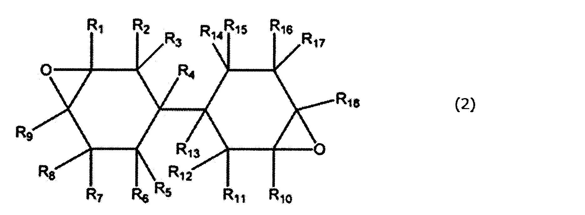
- R 1 to R 18 may be the same or different and each represents a hydrogen atom, a halogen atom, or an organic group that may be substituted with a halogen atom. 6 alkyl groups or alkoxy groups having 1 to 6 carbon atoms are preferred.
- [6] A rearranged wafer produced by using the liquid resin composition according to any one of [1] to [5] and arranging a large number of semiconductor chips on a support and sealing them.
- [7] A rearranged wafer according to [6], wherein a plurality of semiconductor chips arranged on a support are sealed by compression molding.
- [8] A semiconductor package produced by separating the rearranged wafer according to [6] or [7].
- a wafer level package manufactured using a liquid resin encapsulant particularly a semiconductor device manufactured in a wafer level process formed into a wafer shape by compression molding, has less warpage and can be easily conveyed by suction and is productive. High pseudo wafer can be provided.
- the present invention relates to a liquid resin composition having an internal stress value ( ⁇ ) obtained by the formula (1) of 10 MPa or less in a two-layer state of a silicon wafer and a cured product of the liquid resin composition, and a semiconductor device using the same.
- Equation (1) is used to calculate the internal stress value from 150 ° C to 25 ° C by integrating the product of the thermal expansion coefficient between the resin and silicon wafer at each temperature and the elastic modulus of the resin at each temperature. It is a formula.
- ⁇ is the internal stress value
- Eresin (T) is the elastic modulus of the cured product of the liquid resin composition at a temperature T ° C.
- ⁇ resin (T) is the linear expansion coefficient of the cured product of the liquid resin composition at a temperature T ° C.
- ⁇ si (T) represents the linear expansion coefficient of silicon at a temperature of T ° C.
- 2.6 ⁇ 10 ⁇ 6 / ° C. is used as the expansion coefficient of silicon.
- the liquid resin composition used in the present invention preferably contains (A) an epoxy resin, (B) an acid anhydride, (C) an inorganic filler, and (D) a curing accelerator.
- the (A) epoxy resin used in the present invention is not particularly limited in molecular weight or structure as long as it has two or more epoxy groups in one molecule and is liquid at room temperature.
- novolak type epoxy resins such as phenol novolac type epoxy resin and cresol novolak type epoxy resin, bisphenol F type epoxy resin, N, N-diglycidylaniline, N, N-diglycidyltoluidine, diaminodiphenylmethane type glycidylamine, aminophenol Aromatic glycidylamine type epoxy resin such as glycidylamine type, hydroquinone type epoxy resin, biphenyl type epoxy resin, stilbene type epoxy resin, triphenolmethane type epoxy resin, triphenolpropane type epoxy resin, alkyl-modified triphenolmethane type epoxy Resin, triazine nucleus-containing epoxy resin, dicyclopentadiene-modified phenol type epoxy resin, naphthol type epoxy resin, naphthalene type epoxy resin, Epoxy resins such as phenol aralkyl type epoxy resins having a nylene and / or biphenylene skeleton, aralkyl type epoxy resins
- the epoxy resin is finally liquid at room temperature (25 ° C.), but even an epoxy resin that is solid at room temperature is dissolved in the liquid epoxy resin at room temperature, and as a result, in a liquid state I just need it.
- room temperature refers to 25 ° C.
- liquid refers to a resin or resin composition having fluidity.
- the liquid resin composition has fluidity at room temperature (25 ° C.).
- an alicyclic epoxy resin is preferable from the viewpoint of viscosity reduction, reduction of internal stress value ( ⁇ ) obtained by the formula (1) due to increase of glass transition temperature, heat resistance, mechanical properties, and moisture resistance.
- Aromatic glycidyl ether type epoxy resins are preferred from the viewpoints of properties, mechanical properties and moisture resistance.
- resins of the following formulas (3) and (3A) or alicyclic epoxy resins having a structure of the general formula (2) are preferable.
- R21 to R38 each independently represent a hydrogen atom, a halogen atom, a C1-6 alkyl group, a C1-6 haloalkyl group, a C1-6 alkoxy group, or a C1-6 haloalkoxy group.
- Examples of the alicyclic epoxy resin having the structure of the general formula (2) include a resin of the following formula (4).
- the said alicyclic epoxy resin is contained 10weight% or more in all the epoxy resins, and it is more preferable that 25 weight% or more is contained. Further, the alicyclic epoxy resin and the aromatic glycidyl ether type epoxy resin may be used in combination. In this case, the blending ratio [(alicyclic epoxy resin) / (aromatic glycidyl ether type epoxy resin)] is preferably from 0.1 to 9, more preferably from 0.3 to 5.
- the internal stress value ( ⁇ ) obtained by the formula (1) may be increased, This is because when the upper limit is exceeded, there are many volatile components in the molding and the productivity may deteriorate.
- Examples of the acid anhydride (B) used in the present invention include phthalic anhydride, maleic anhydride, trimellitic anhydride, pyromellitic anhydride, hexahydrophthalic anhydride, 3-methyl-hexahydrophthalic anhydride, 4-methyl-hexahydro.
- Examples thereof include phthalic anhydride, a mixture of 3-methyl-hexahydrophthalic anhydride and 4-methyl-hexahydrophthalic anhydride, tetrahydrophthalic anhydride, nadic anhydride, or methyl nadic anhydride.
- tetrahydrophthalic anhydride as a curing agent. In particular, these may be used alone or in combination of two or more.
- any monomer, oligomer, or polymer having a functional group that reacts with epoxy in one molecule can be used in combination.
- phenols such as phenol novolac resin, cresol novolak resin, dicyclopentadiene modified phenol resin, terpene modified phenol resin, triphenolmethane type resin, phenol aralkyl resin (having phenylene skeleton, diphenylene skeleton, etc.) can be mentioned.
- an inorganic filler (C) used for this invention what is generally used for the sealing material can be used.
- examples thereof include fused silica, crystalline silica, talc, alumina, silicon nitride and the like, and these may be used alone or in combination of two or more.
- fused silica, crystalline silica, and synthetic silica powder are preferable because the heat resistance, moisture resistance, strength, and the like of the resin composition can be improved.
- the shape of the inorganic filler is not particularly limited, but the shape is preferably spherical from the viewpoints of viscosity characteristics and flow characteristics.
- the content of the inorganic filler (C) in the liquid resin composition is preferably 60% by weight or more and 95% by weight or less, and more preferably 80% by weight or more and 95% by weight or less.
- the content when the inorganic filler is fused silica is preferably 60% by weight or more and 95% by weight or less in the total epoxy resin composition, more preferably 80%, in view of the balance between moldability and solder crack resistance. % By weight or more and 95% by weight or less. If it is less than the lower limit value, the solder crack resistance with increasing water absorption rate is lowered, and if it exceeds the upper limit value, there may be a problem in the dispensing performance of the liquid sealing resin composition.
- a hardening accelerator (D) used for this invention what is necessary is just to accelerate
- phosphonium salts, triphenylphosphine, imidazole compounds, sulfonium salts and the like can be mentioned, but are not limited thereto.
- These curing accelerators may be used alone or in combination.
- the phosphonium salt having the structure of the general formula (5) or the general formula (6), the triphenylphosphine having the structure of the formula (7), or the imidazole compound having the structure of the formula (8) or the formula (9) has a low viscosity. This is effective from the viewpoint of optimization.
- a hardening accelerator of the said General formula (5) the substance which has structures, such as following formula (10), Formula (11), and Formula (12), is mentioned, for example.
- R1, R2, R3, and R4 are monovalent organic groups or monovalent aliphatic groups having an aromatic ring or a heterocyclic ring, and at least one of them is (A proton donor having at least one proton that can be released out of the molecule is a group formed by releasing one proton, and these may be the same or different from each other.)
- Ar represents a substituted or unsubstituted aromatic group, and two oxygen atoms in the same molecule are located adjacent to the aromatic carbon position.
- N is an integer of 2 to 12
- examples of the curing accelerator of the general formula (6) include substances having structures such as the following formula (13), formula (14), and formula (15).
- the compounding quantity of a hardening accelerator is 0.1 to 1.0 weight part with respect to 100 weight part of all the liquid sealing resin compositions, More preferably, it is 0.3. It is not less than 0.8 parts by weight. This is because if it is less than the lower limit, curing is slow and productivity may be lowered, and if it exceeds the upper limit, storage stability may be deteriorated.
- the blending ratio [(B) / (D)] of (B) acid anhydride and (D) curing accelerator is preferably 3 or more and 35 or less, more preferably 5 or more and 30 or less, and more preferably 10 or more and 20 or less. Particularly preferred. This is because if the blending ratio [(B) / (D)] is less than the lower limit, the storage stability may be deteriorated, and if it exceeds the upper limit, curing may be slow and productivity may be deteriorated. . Further, the blending amount of (B) acid anhydride is preferably 2 parts by weight or more and 10 parts by weight or less, and more preferably 5 parts by weight or more and 7 parts by weight or less with respect to 100 parts by weight of the liquid resin composition.
- a release agent such as a silicone compound or wax as a defoaming agent, a low stress material, a flame retardant, etc., which can be added according to the required properties.
- each component, additive and the like are dispersed and kneaded using an apparatus such as a planetary mixer, three rolls, two hot rolls, and a laika machine, and then vacuumed. Manufacture by defoaming under.
- the internal stress value ( ⁇ ) obtained by the formula (1) in the two-layer state of the cured product of the liquid resin composition of the present invention and the silicon wafer needs to be 10 MPa or less. If this value exceeds the upper limit, the wafer warpage due to internal stress may increase when applied to a wafer level package.
- ⁇ is the internal stress value
- Eresin (T) is the elastic modulus of the resin at a temperature T ° C.
- ⁇ resin (T) is the linear expansion coefficient of the resin at the temperature T ° C.
- ⁇ si (T) is the semiconductor element at the temperature T ° C.
- Examples of the semiconductor package of the present invention include the following types, but are not limited thereto. That is, BGA (Ball Grid Array), FCBGA (Flip Chip BGA), MAPBGA (Molded Array Process BGA), and the like.
- BGA Bit Grid Array
- FCBGA Flexible Chip BGA
- MAPBGA Molded Array Process BGA
- a more preferable example of application of the liquid sealing resin composition of the present invention is eWLB (Embedded Wafer-Level BGA), which is in the form of Fan-Out type, Fan-In type, SiP (System in Package), etc. is there.
- a method for manufacturing a semiconductor package of the present invention for example, there is the following method, but the method is not limited to this. That is, a step of arranging a large number of semiconductor chips known to operate in advance on a carrier as a support with the active surface facing downward (a step of arranging a large number of semiconductor chips on a support), and then a molding metal Place on the mold and apply the liquid resin composition of the present invention on the dispenser with a dispenser or the like (the step of applying the liquid resin composition), then, after the compression molding (the step of forming with the mold), peel off the carrier Thus, a rearranged wafer in which the semiconductor chips are sealed and rearranged is obtained.
- a buffer coating material is spin-coated on the surface of the obtained rearranged wafer, the buffer coating material is cured to form an insulating film layer, and then an electrode pad portion on the active surface of the semiconductor chip is opened by a patterning process. Make a hole. Rewiring processing and mounting bump formation are performed by plating or the like from the hole portion to the surface of the buffer coating material (rewiring process). Then, a semiconductor package is obtained by dividing this into pieces by dicing (an individualization process).
- Example 1 (1) As epoxy resin (A), alicyclic epoxy resin represented by formula (4) 50 parts by weight (2) As epoxy resin (A), bisphenol F type epoxy resin SB-403S manufactured by Nippon Kayaku Kogyo Co., Ltd. 50 parts by weight (3) As an acid anhydride (B), methyltetrahydrophthalic anhydride MT-500 100 parts by weight (4) As an inorganic filler (C) Inorganic filler 1 FB-74 ( Fused spherical silica, average particle size 30 ⁇ m) 1600 parts by weight manufactured by Denki Kagaku Kogyo Co., Ltd.
- inorganic filler (C) As inorganic filler (C), inorganic filler 2 SO-E2 (fused spherical silica, average particle size 0.5 ⁇ m) ADMATEX 300 parts by weight (6) Curing accelerator represented by formula (11) as curing accelerator (D) 7 parts by weight (7) Epoxy silane coupling agent: 3-glycidoxypropyltrimethoxysilane KBM-403E 7 parts by weight made by Shin-Etsu Chemical Co., Ltd. was placed in a beaker and mixed with a spatula, kneaded three times with a three-roller, then put into a beaker and defoamed in a vacuum oven (room temperature, 5 mmHg) for 10 minutes. Processing was performed to obtain a liquid resin composition.
- the liquid resin composition was cured under curing conditions of 125 ° C. for 10 minutes and 150 ° C. for 1 hour to prepare a test sample.
- the temperature of the liquid resin composition was measured by a compression method from ⁇ 100 ° C. to 350 ° C. at 5 ° C./min, and the linear expansion coefficient in the glass state region was measured.
- the compression method is measured based on JIS K7197.
- the glass transition temperature (° C.) is 5 from 0 ° C. to 350 ° C.
- Eresin (T) is the elastic modulus of the resin at a temperature T ° C.
- ⁇ resin (T) is the linear expansion coefficient of the resin at the temperature T ° C.
- ⁇ si (T) is the silicon coefficient at the temperature T ° C. (Linear expansion coefficient.)
- Adhesion force The prepared liquid resin composition was applied to the bright etch surface, which is the back surface of a 625 ⁇ m thick silicon wafer having a surface cut to 10 mm square. A nail (copper) for adhesion measurement was attached across this, and after heat curing at 125 ° C. for 10 minutes, post-curing was further performed at 175 ° C. for 4 hours to obtain a measurement sample. The adhesion area of the nail is 10 mm 2 . This was attached to a measuring device (Dage 4000, manufactured by Dage) with the semiconductor chip surface fixed in a vise and lifted vertically at 25 ° C. to measure the adhesion. The prepared liquid resin composition has a viscosity at 25 ° C.
- a semiconductor chip was mounted with a die mounter (DB200, manufactured by Kasuya Kogyo Co., Ltd.) so that the active surface on which the electrodes of the semiconductor chip were in contact with the thermally foamed film with a suitable space in the support substrate.
- a support substrate with a semiconductor chip was set in a compression molding machine, an appropriate amount of the liquid resin composition was placed thereon, and cured at a molding pressure of 3 MPa at 125 ° C. for 10 minutes to obtain a wafer.
- the amount of the liquid resin composition was adjusted so that the resin thickness after molding was 600 ⁇ 10 ⁇ m. After the wafer is heat-treated in an oven at 150 ° C. for 1 hour and then cured, it is placed on a 200 ° C.
- the obtained rearranged wafer was measured at a measurement distance of 195 mm and a measurement speed of 6 mm / s using a surface roughness measuring device (SURFCOM 1400D, manufactured by Tokyo Seimitsu Co., Ltd.) with the chip surface facing upward. It was 7 mm.
- the entire rearranged wafer thus obtained was spin-coated with a photosensitive buffer coating material (DSPIN80A, manufactured by SOKUDO Co., Ltd., 1500 rpm, 30 seconds), and then pre-baked (at 125 ° C. for 5 minutes) with the same apparatus.
- An insulating film for rewiring was formed on the surface.
- light irradiation (broadband aligner MA-8, manufactured by SUSS Microtec Co., Ltd., 500 mJ / cm 2 ) was performed, and a developer (TMAH 2.38) was formed. %, 23 ° C., 62 seconds twice paddle), and final curing (250 ° C., 1.5 hours).
- a film was formed in order on the buffer coat by sputtering (SPF-740H, manufactured by Canon Anelva Engineering Co., Ltd.) so that the thickness was 500 mm of titanium and 3000 mm of copper.
- a resist (Sunfort 155, manufactured by Asahi Kasei E-Materials Co., Ltd.) was applied thereto, and the resist was exposed and developed using a rewiring circuit mask. Further, a copper layer having a thickness of 10 ⁇ m was formed on the whole by copper plating, and then the resist was peeled off. In this state, unnecessary copper and titanium layers remain on the buffer coat surface.
- a buffer coat layer is provided again by spin coating, and holes are opened at different positions after rewiring.
- the copper layer for this was exposed.
- Rewiring was performed according to the above procedure.
- the rearranged wafers that had been rewired were separated into 15 mm square sizes using a dicer. In this way, a semiconductor package device for reliability testing was assembled.
- solder heat resistance test The produced semiconductor package was treated at 125 ° C. for 20 hours, and then moisture-absorbed for 168 hours at 85 ° C. and 85% RH. This was passed three times through a reflow oven set so that the maximum temperature of 260 ° C. was 30 seconds, and a solder heat resistance test 1 was conducted. (Test condition 1) Further, a solder heat resistance test 2 was performed in the same manner except that the moisture absorption treatment condition of the solder heat resistance test 1 (test condition 1) was 85 ° C. and 60% RH168h. (Test condition 2) The sample after the test was checked for internal peeling using a 20 MHz probe with an ultrasonic flaw detector (FineSAT FS300, manufactured by Hitachi Construction Machinery Co., Ltd.).
- Example 2-16 [Comparative Examples 1 and 2] According to the formulations in Tables 1 and 2, a liquid resin composition was obtained in the same manner as in Example 1 and evaluated in the same manner as in Example 1. The results are shown in Tables 1-2. The raw materials used other than Example 1 are shown below.
- D a curing accelerator represented by the formula (13): ⁇ Sulphonium salt type cationic polymerization initiator: Sun-Aid SI-100L, Sanshin Chemical Industry Co., Ltd.
- Phenol novolac resin MEH-8000, Meiwa Kasei Co., Ltd. as other curing agent
- the equivalent ratio indicates the ratio of the number of moles of epoxy groups to the number of moles of carboxyl groups.
- a wafer level package manufactured using a liquid resin encapsulant particularly a semiconductor device manufactured in a wafer level process formed into a wafer shape by compression molding, has less warpage and can be easily conveyed by suction and is productive. High pseudo wafer can be provided.
Landscapes
- Chemical & Material Sciences (AREA)
- Health & Medical Sciences (AREA)
- Chemical Kinetics & Catalysis (AREA)
- Medicinal Chemistry (AREA)
- Polymers & Plastics (AREA)
- Organic Chemistry (AREA)
- Structures Or Materials For Encapsulating Or Coating Semiconductor Devices Or Solid State Devices (AREA)
- Epoxy Resins (AREA)
- Compositions Of Macromolecular Compounds (AREA)
Abstract
本発明により、ウエハーレベルパッケージにおいて生産性の低下を招く擬似ウエハーの反りを抑制した液状封止樹脂組成物が提供される。シリコンウェハーと本発明の液状樹脂組成物の硬化物の2層状態において式(1)により得られる内部応力値(σ)が10MPa以下である(式中、σは内部応力値、Eresin(T)は温度T℃における液状樹脂組成物の硬化物の弾性率、αresin(T)は温度T℃における液状樹脂組成物の硬化物の線膨張係数、αsi(T)は温度T℃におけるシリコンの線膨張係数を示す)。
Description
本発明は、液状樹脂組成物と、それを用いて作製した半導体パッケージおよび半導体パッケージの製造方法に関する。
本願は、2011年3月30日に、日本に出願された特願2011-074586号に基づき優先権を主張し、その内容をここに援用する。
本願は、2011年3月30日に、日本に出願された特願2011-074586号に基づき優先権を主張し、その内容をここに援用する。
近年の電子機器の小型化、軽量化、高集積化、高速動作化の動向を反映して、半導体パッケージに占める半導体チップの面積、体積は大きくなり、半導体パッケージ内の配線は微細化、短小化している。
従来、このような半導体チップを配線基板に電気的に接続する方法としては、半導体チップに突起電極(バンプ)を形成して、このバンプによって配線基板と一括接合するフリップチップ接続と呼ばれる実装方法がある。この方法では、例えば、半導体チップを小型化した場合、配線基板上の配線パターンも変更せねばならず、開発の際のタイムラグやコスト増につながり、多品種少量生産には向かなくなってしまう。
そこで、ウエハーレベルパッケージ(WLP)と呼ばれる、半導体回路の形成されたウエハーを個別の半導体チップに切断する前に、電気接続用のバンプを設け、ウエハー全体を封止する手法が考え出された。(例えば、特許文献1参照。)
WLPでは配線基板を用いたフリップチップ接続が不要なため、多品種少量生産にも適する。しかしWLPでは、半導体パッケージの機能拡大と共に増大する単位面積あたりの実装用IO(入出力)バンプ数の上限が半導体チップの面積に比例し、小チップに機能を詰め込んだ多IO半導体チップには対応できない。
そこで、予め切断した半導体チップを支持体となるキャリア上に並べ、それをウエハー形状に封止樹脂で封止した後(擬似ウエハー化)、半導体チップの回路面に再配線を行うことで、半導体チップのデザイン変更にも低コストで対応しつつ、半導体チップのサイズに対して、過多なIO数にも対応できる技術が提案されている。(例えば、特許文献2参照。)
ところが、このタイプのWLPでは、封止樹脂とキャリアとの線膨張係数の差による内部応力から、擬似ウエハーに反りが発生することにより、封止より後の工程での擬似ウエハーの吸着搬送が困難になり生産性が低下することが問題となっている。
従来、このような半導体チップを配線基板に電気的に接続する方法としては、半導体チップに突起電極(バンプ)を形成して、このバンプによって配線基板と一括接合するフリップチップ接続と呼ばれる実装方法がある。この方法では、例えば、半導体チップを小型化した場合、配線基板上の配線パターンも変更せねばならず、開発の際のタイムラグやコスト増につながり、多品種少量生産には向かなくなってしまう。
そこで、ウエハーレベルパッケージ(WLP)と呼ばれる、半導体回路の形成されたウエハーを個別の半導体チップに切断する前に、電気接続用のバンプを設け、ウエハー全体を封止する手法が考え出された。(例えば、特許文献1参照。)
WLPでは配線基板を用いたフリップチップ接続が不要なため、多品種少量生産にも適する。しかしWLPでは、半導体パッケージの機能拡大と共に増大する単位面積あたりの実装用IO(入出力)バンプ数の上限が半導体チップの面積に比例し、小チップに機能を詰め込んだ多IO半導体チップには対応できない。
そこで、予め切断した半導体チップを支持体となるキャリア上に並べ、それをウエハー形状に封止樹脂で封止した後(擬似ウエハー化)、半導体チップの回路面に再配線を行うことで、半導体チップのデザイン変更にも低コストで対応しつつ、半導体チップのサイズに対して、過多なIO数にも対応できる技術が提案されている。(例えば、特許文献2参照。)
ところが、このタイプのWLPでは、封止樹脂とキャリアとの線膨張係数の差による内部応力から、擬似ウエハーに反りが発生することにより、封止より後の工程での擬似ウエハーの吸着搬送が困難になり生産性が低下することが問題となっている。
本発明は、WLPにおいて生産性の低下を招く擬似ウエハーの反りを抑制した液状封止樹脂組成物、およびこれを用いて作製した半導体パッケージを提供するものである。
本発明は以下の通りである。
[1]シリコンウェハーと液状樹脂組成物の硬化物の2層状態において式(1)により得られる内部応力値(σ)が10MPa以下である液状樹脂組成物。
[1]シリコンウェハーと液状樹脂組成物の硬化物の2層状態において式(1)により得られる内部応力値(σ)が10MPa以下である液状樹脂組成物。

(式中、σは内部応力値、Eresin(T)は温度T℃における液状樹脂組成物の硬化物の弾性率、αresin(T)は温度T℃における液状樹脂組成物の硬化物の線膨張係数、αsi(T)は温度T℃におけるシリコンの線膨張係数を示す。)
[2]硬化物の粘弾性測定装置(DMA)で測定したガラス転移温度Tmgが150℃以上350℃以下である[1]に記載の液状樹脂組成物。
[3]前記液状樹脂組成物が(A)エポキシ樹脂、(B)酸無水物、(C)無機充填材、及び(D)硬化促進剤を含有し、無機充填材が全液状樹脂組成物に対して60重量%以上95重量%以下含まれる[1]又は[2]に記載の液状樹脂組成物。
[4](A)エポキシ樹脂が脂環式エポキシ樹脂を含むものである[3]に記載の液状樹脂組成物。
[5]前記脂環式エポキシ樹脂が、下記式(2)で表される3,4,3’,4’-ジエポキシビシクロヘキシル化合物を含む[4]に記載の液状樹脂組成物。
[2]硬化物の粘弾性測定装置(DMA)で測定したガラス転移温度Tmgが150℃以上350℃以下である[1]に記載の液状樹脂組成物。
[3]前記液状樹脂組成物が(A)エポキシ樹脂、(B)酸無水物、(C)無機充填材、及び(D)硬化促進剤を含有し、無機充填材が全液状樹脂組成物に対して60重量%以上95重量%以下含まれる[1]又は[2]に記載の液状樹脂組成物。
[4](A)エポキシ樹脂が脂環式エポキシ樹脂を含むものである[3]に記載の液状樹脂組成物。
[5]前記脂環式エポキシ樹脂が、下記式(2)で表される3,4,3’,4’-ジエポキシビシクロヘキシル化合物を含む[4]に記載の液状樹脂組成物。
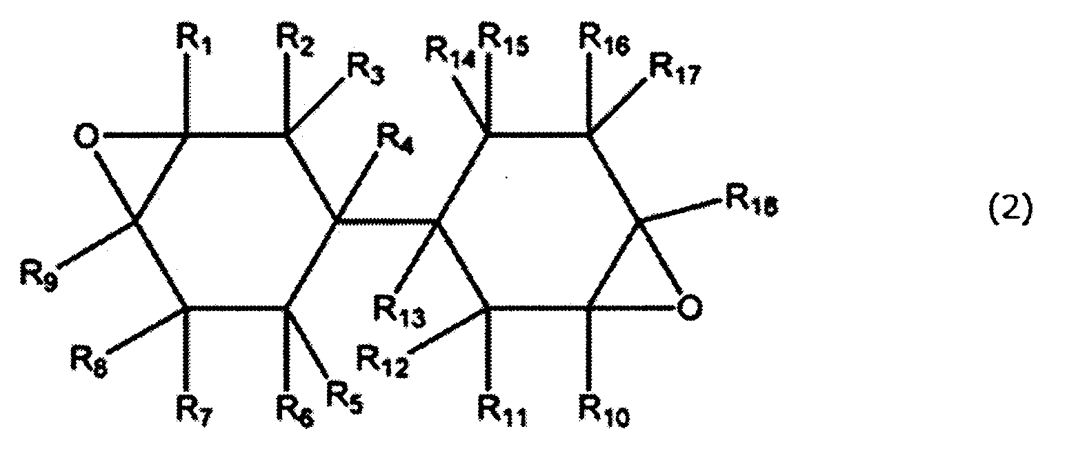
(式中、R1 ~ R18は、同一でも異なっていてもよく、水素原子、ハロゲン原子、ハロゲン原子で置換されてもよい有機基のいずれかを示す。有機基としては、炭素数1~6のアルキル基または炭素数1~6のアルコキシ基が好ましい。)
[6][1]乃至[5]のいずれかに記載の液状樹脂組成物を用いて、半導体チップを支持体に多数個配置し、封止して作製した再配置ウエハー。
[7][6]に記載の再配置ウエハーにおいて、半導体チップを支持体に多数個配置したものを圧縮成形により、封止して作製された再配置ウエハー。
[8][6]又は[7]に記載の再配置ウエハーを個片化して作製した半導体パッケージ。
[9][1]乃至[5]のいずれかに記載の液状樹脂組成物を用いて作製される半導体パッケージの製造方法であって、半導体チップを支持体に多数個配置する工程、この上に前記液状樹脂組成物を塗布する工程、金型により成形する工程、を含む半導体パッケージの製造方法。
[6][1]乃至[5]のいずれかに記載の液状樹脂組成物を用いて、半導体チップを支持体に多数個配置し、封止して作製した再配置ウエハー。
[7][6]に記載の再配置ウエハーにおいて、半導体チップを支持体に多数個配置したものを圧縮成形により、封止して作製された再配置ウエハー。
[8][6]又は[7]に記載の再配置ウエハーを個片化して作製した半導体パッケージ。
[9][1]乃至[5]のいずれかに記載の液状樹脂組成物を用いて作製される半導体パッケージの製造方法であって、半導体チップを支持体に多数個配置する工程、この上に前記液状樹脂組成物を塗布する工程、金型により成形する工程、を含む半導体パッケージの製造方法。
本発明により、液状樹脂封止材を用いて作製されたウエハーレベルパッケージ、とりわけ圧縮成形でウエハー状に形成されたウエハーレベル工程で製造される半導体装置において、反りが少なく吸着搬送が容易で生産性高い擬似ウエハーを提供する事が出来る。
本発明は、シリコンウェハーと液状樹脂組成物の硬化物の2層状態において式(1)により得られる内部応力値(σ)が10MPa以下である液状樹脂組成物、およびこれを用いた半導体装置に関する。式(1)は、各温度での樹脂とシリコンウエハーの熱膨張率の差と、各温度での樹脂の弾性率の積の積分により、150℃から25℃までの内部応力値を求める為の式である。

(式中、σは内部応力値、Eresin(T)は温度T℃における液状樹脂組成物の硬化物の弾性率、αresin(T)は温度T℃における液状樹脂組成物の硬化物の線膨張係数、αsi(T)は温度T℃におけるシリコンの線膨張係数を示す。ここでは、シリコンの膨張率として 2.6 x 10⁻⁶/℃を用いる。)
以下、本発明を詳細に説明する。
以下、本発明を詳細に説明する。
本発明に用いる液状樹脂組成物としては、(A)エポキシ樹脂、(B)酸無水物、(C)無機充填材、及び(D)硬化促進剤を含有するものであることが好ましい。
本発明に用いる(A)エポキシ樹脂としては、一分子中にエポキシ基を2個以上有するもので、かつ常温において液状であれば、特に分子量や構造は限定されるものではない。例えば、フェノールノボラック型エポキシ樹脂、クレゾールノボラック型エポキシ樹脂などのノボラック型エポキシ樹脂、ビスフェノールF型エポキシ樹脂、N,N-ジグリシジルアニリン、N,N-ジグリシジルトルイジン、ジアミノジフェニルメタン型グリシジルアミン、アミノフェノール型グリシジルアミンのような芳香族グリシジルアミン型エポキシ樹脂、ハイドロキノン型エポキシ樹脂、ビフェニル型エポキシ樹脂、スチルベン型エポキシ樹脂、トリフェノールメタン型エポキシ樹脂、トリフェノールプロパン型エポキシ樹脂、アルキル変性トリフェノールメタン型エポキシ樹脂、トリアジン核含有エポキシ樹脂、ジシクロペンタジエン変性フェノール型エポキシ樹脂、ナフトール型エポキシ樹脂、ナフタレン型エポキシ樹脂、フェニレンおよび/またはビフェニレン骨格を有するフェノールアラルキル型エポキシ樹脂、フェニレンおよび/またはビフェニレン骨格を有するナフトールアラルキル型エポキシ樹脂などのアラルキル型エポキシ樹脂などのエポキシ樹脂、ビニルシクロヘキセンジオキシド、ジシクロペンタジエンオキシド、アリサイクリックジエポキシ-アジペイドなどの脂環式エポキシ樹脂などの脂肪族エポキシ樹脂が挙げられる。これらは単独でも2種以上混合して使用しても良い。
本発明に用いる(A)エポキシ樹脂としては、一分子中にエポキシ基を2個以上有するもので、かつ常温において液状であれば、特に分子量や構造は限定されるものではない。例えば、フェノールノボラック型エポキシ樹脂、クレゾールノボラック型エポキシ樹脂などのノボラック型エポキシ樹脂、ビスフェノールF型エポキシ樹脂、N,N-ジグリシジルアニリン、N,N-ジグリシジルトルイジン、ジアミノジフェニルメタン型グリシジルアミン、アミノフェノール型グリシジルアミンのような芳香族グリシジルアミン型エポキシ樹脂、ハイドロキノン型エポキシ樹脂、ビフェニル型エポキシ樹脂、スチルベン型エポキシ樹脂、トリフェノールメタン型エポキシ樹脂、トリフェノールプロパン型エポキシ樹脂、アルキル変性トリフェノールメタン型エポキシ樹脂、トリアジン核含有エポキシ樹脂、ジシクロペンタジエン変性フェノール型エポキシ樹脂、ナフトール型エポキシ樹脂、ナフタレン型エポキシ樹脂、フェニレンおよび/またはビフェニレン骨格を有するフェノールアラルキル型エポキシ樹脂、フェニレンおよび/またはビフェニレン骨格を有するナフトールアラルキル型エポキシ樹脂などのアラルキル型エポキシ樹脂などのエポキシ樹脂、ビニルシクロヘキセンジオキシド、ジシクロペンタジエンオキシド、アリサイクリックジエポキシ-アジペイドなどの脂環式エポキシ樹脂などの脂肪族エポキシ樹脂が挙げられる。これらは単独でも2種以上混合して使用しても良い。
本発明ではエポキシ樹脂として最終的に常温(25℃)で液状であることが好ましいが、常温で固体のエポキシ樹脂であっても常温で液状のエポキシ樹脂に溶解させ、結果的に液状の状態であればよい。本発明において、室温とは25℃を指し、また、液状とは樹脂又は樹脂組成物が流動性を有していることを指す。本発明において、上記液状樹脂組成物は、室温(25℃)において、流動性を有している。
本発明では、粘度低下、ガラス転移温度の上昇による式(1)により得られる内部応力値(σ)の低減、耐熱性、機械特性、耐湿性という観点から脂環式エポキシ樹脂が好ましく、又耐熱性、機械特性、耐湿性という観点から芳香族グリシジルエーテル型エポキシ樹脂が好ましい。
脂環式エポキシ樹脂としては、下記式(3)、(3A)の樹脂、又は一般式(2)の構造を有する脂環式エポキシ樹脂が好ましい。式(3)中、R21~R38は、各々独立して、水素原子、ハロゲン原子、C1~6アルキル基、C1~6ハロアルキル基、C1~6アルコキシ基、または、C1~6ハロアルコキシ基を示す。一般式(2)の構造を有する脂環式エポキシ樹脂としては、例えば下記式(4)の樹脂が挙げられる。
脂環式エポキシ樹脂としては、下記式(3)、(3A)の樹脂、又は一般式(2)の構造を有する脂環式エポキシ樹脂が好ましい。式(3)中、R21~R38は、各々独立して、水素原子、ハロゲン原子、C1~6アルキル基、C1~6ハロアルキル基、C1~6アルコキシ基、または、C1~6ハロアルコキシ基を示す。一般式(2)の構造を有する脂環式エポキシ樹脂としては、例えば下記式(4)の樹脂が挙げられる。


本発明においては、上記脂環式エポキシ樹脂が全エポキシ樹脂中に10重量%以上含まれることが好ましく、25重量%以上含まれることがより好ましい。
又、上記脂環式エポキシ樹脂と上記芳香族グリシジルエーテル型エポキシ樹脂を併用してもよい。この場合の配合比[(脂環式エポキシ樹脂)/(芳香族グリシジルエーテル型エポキシ樹脂)]は、0.1以上9以下が好ましく、0.3以上5以下であることがさらに好ましい。配合比[(脂環式エポキシ樹脂)/(芳香族グリシジルエーテル型エポキシ樹脂)]が、下限値未満の場合には式(1)により得られる内部応力値(σ)が高くなる恐れがあり、上限値を越える場合には成形中の揮発成分が多く生産性が悪くなる恐れがあるためである。
又、上記脂環式エポキシ樹脂と上記芳香族グリシジルエーテル型エポキシ樹脂を併用してもよい。この場合の配合比[(脂環式エポキシ樹脂)/(芳香族グリシジルエーテル型エポキシ樹脂)]は、0.1以上9以下が好ましく、0.3以上5以下であることがさらに好ましい。配合比[(脂環式エポキシ樹脂)/(芳香族グリシジルエーテル型エポキシ樹脂)]が、下限値未満の場合には式(1)により得られる内部応力値(σ)が高くなる恐れがあり、上限値を越える場合には成形中の揮発成分が多く生産性が悪くなる恐れがあるためである。
本発明に用いる(B)酸無水物としては、無水フタル酸、無水マレイン酸、無水トリメリット酸、無水ピロメリット酸、ヘキサヒドロ無水フタル酸、3-メチル-ヘキサヒドロ無水フタル酸、4-メチル-ヘキサヒドロ無水フタル酸、3-メチル-ヘキサヒドロ無水フタル酸と4-メチル-ヘキサヒドロ無水フタル酸との混合物、テトラヒドロ無水フタル酸、無水ナジック酸、または無水メチルナジック酸などが挙げられる。
これらは、低温での硬化が早いことと、硬化物のガラス転移温度が高くなることから好ましい。また、常温で液状であり、且つ粘度も低いことから、テトラヒドロ無水フタル酸を硬化剤として用いることがより好ましい。特にこれらは、単独で用いても2種以上用いても差し支えない。
これらは、低温での硬化が早いことと、硬化物のガラス転移温度が高くなることから好ましい。また、常温で液状であり、且つ粘度も低いことから、テトラヒドロ無水フタル酸を硬化剤として用いることがより好ましい。特にこれらは、単独で用いても2種以上用いても差し支えない。
上記の(B)酸無水物以外の硬化剤としては、1分子内にエポキシと反応する官能基を有するモノマー、オリゴマー、ポリマー全般であればこれを併用できる。例えば、フェノールノボラック樹脂、クレゾールノボラック樹脂、ジシクロペンタジエン変性フェノール樹脂、テルペン変性フェノール樹脂、トリフェノールメタン型樹脂、フェノールアラルキル樹脂(フェニレン骨格、ジフェニレン骨格などを有する)などのフェノール類が挙げられる。
本発明に用いる無機充填材(C)としては、一般に封止材料に使用されているものを使用することができる。
例えば、溶融シリカ、結晶シリカ、タルク、アルミナ、窒化珪素などが挙げられ、これらは単独でも2種類以上併用して用いても差し支えない。これらの中でも樹脂組成物の耐熱性、耐湿性、強度などを向上できることから溶融シリカ、結晶シリカ、合成シリカ粉末が好ましい。
前記無機充填材の形状は、特に限定されないが、粘度特性や流動特性の観点から形状は球状であることが好ましい。
液状樹脂組成物における無機充填材(C)の含有量は、60重量%以上95重量%以下であることが好ましく、80重量%以上95重量%以下であることがより好ましい。無機充填剤(C)の含有量が上記範囲内であることにより、粘度の上昇や反りを抑制し、液状樹脂組成物のディスペンス性能を向上させることができる。
無機充填材が溶融シリカの場合の含有量としては、成形性と耐半田クラック性のバランスから、全エポキシ樹脂組成物中に60重量%以上95重量%以下使用することが好ましく、更に好ましくは80重量%以上95重量%以下である。前記下限値未満の場合には、吸水率の上昇に伴う耐半田クラック性が低下し、前記上限値を越えると液状封止用樹脂組成物のディスペンス性能に問題が生じる可能性がある。
例えば、溶融シリカ、結晶シリカ、タルク、アルミナ、窒化珪素などが挙げられ、これらは単独でも2種類以上併用して用いても差し支えない。これらの中でも樹脂組成物の耐熱性、耐湿性、強度などを向上できることから溶融シリカ、結晶シリカ、合成シリカ粉末が好ましい。
前記無機充填材の形状は、特に限定されないが、粘度特性や流動特性の観点から形状は球状であることが好ましい。
液状樹脂組成物における無機充填材(C)の含有量は、60重量%以上95重量%以下であることが好ましく、80重量%以上95重量%以下であることがより好ましい。無機充填剤(C)の含有量が上記範囲内であることにより、粘度の上昇や反りを抑制し、液状樹脂組成物のディスペンス性能を向上させることができる。
無機充填材が溶融シリカの場合の含有量としては、成形性と耐半田クラック性のバランスから、全エポキシ樹脂組成物中に60重量%以上95重量%以下使用することが好ましく、更に好ましくは80重量%以上95重量%以下である。前記下限値未満の場合には、吸水率の上昇に伴う耐半田クラック性が低下し、前記上限値を越えると液状封止用樹脂組成物のディスペンス性能に問題が生じる可能性がある。
本発明に用いる硬化促進剤(D)としては、エポキシ基と酸無水物との反応もしくは、エポキシの単独重合を促進させるものであればよく、一般に封止用材料に用いられるものを広く使用できる。例えば、ホスホニウム塩、トリフェニルホスフィン、イミダゾール化合物、スルホニウム塩等が挙げられるが、これらに限定されるものではない。これらの硬化促進剤は単独でも混合して用いても差し支えない。好ましくは一般式(5)または一般式(6)の構造を有するホスホニウム塩、式(7)の構造を有するトリフェニルホスフィン、式(8)または式(9)の構造を有するイミダゾール化合物が低粘度化の観点から有効である。前記一般式(5)の硬化促進剤としては、例えば、下記式(10)、式(11)、および式(12)などの構造を有する物質が挙げられる。

(ただし、式(5)でR1, R2, R3, 及びR4は芳香族環もしくは複素環を有する1価の有機基または1価の脂肪族基であって、それらの内の少なくとも1つは、分子外に放出しうるプロトンを少なくとも1個有するプロトン供与体がプロトンを1個放出してなる基であり、これらは互いに同一であっても異なっていても良い。)

(ただし、式(6)で、Arは置換または無置換の芳香族基を表し、同一分子内の二つの酸素原子は、芳香族炭素位に隣接して位置する。 nは2~12の整数である。)





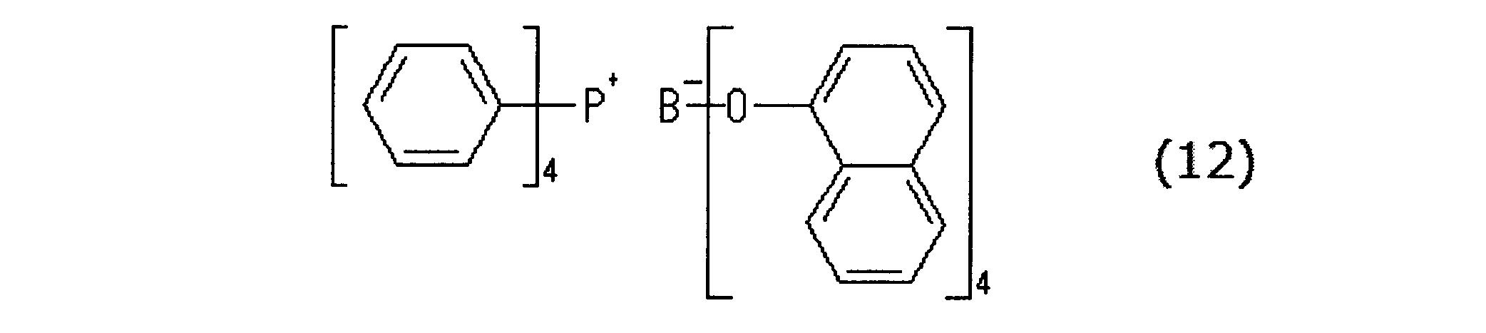
また一般式(6)の硬化促進剤としては、下記式(13)、式(14)、および式(15)などの構造を有する物質が挙げられる。

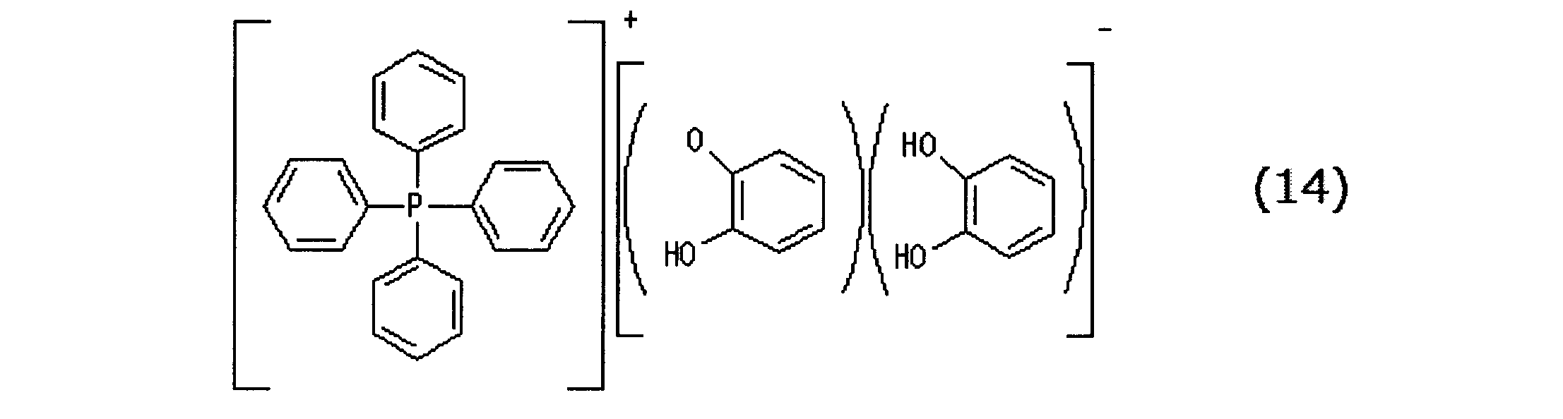
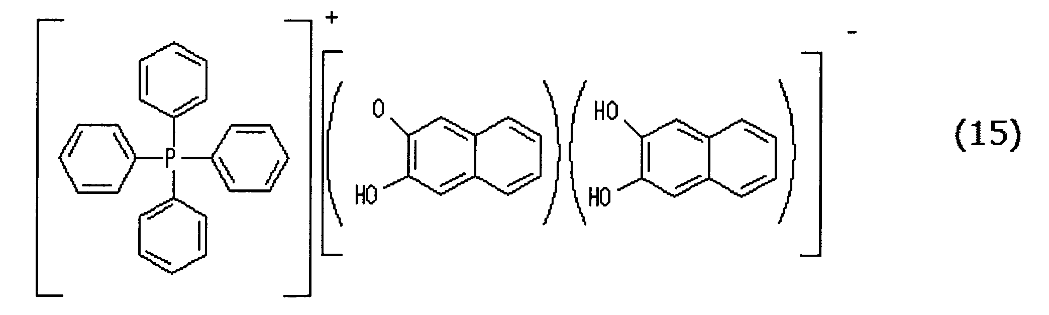
(D)硬化促進剤の配合量は、全液状封止用樹脂組成物100重量部に対して、0.1重量部以上1.0重量部以下であることが好ましく、更に好ましくは0.3重量部以上0.8重量部以下である。下限値未満の場合には硬化が遅く生産性が低下する恐れがあり、上限値を越える場合には保存性が悪化する恐れがあるためである。
(B)酸無水物と(D)硬化促進剤の配合比[(B)/(D)]は、3以上35以下が好ましく、5以上30以下であることがさらに好ましく、10以上20以下が特に好ましい。配合比[(B)/(D)]が、下限値未満の場合には保存性が悪化する恐れがあり、上限値を越える場合には硬化が遅く生産性が悪くなる恐れがあるためである。
また、(B)酸無水物の配合量は、液状樹脂組成物100重量部に対して、2重量部以上10重量部以下が好ましく、更に好ましくは5重量部以上7重量部以下である。
(B)酸無水物の配合量が、下限値未満の場合には硬化性が悪くなり、生産性が低下する恐れがある。そして、上限値を越える場合には、耐湿信頼性が低下する恐れがある。
また、(B)酸無水物の配合量は、液状樹脂組成物100重量部に対して、2重量部以上10重量部以下が好ましく、更に好ましくは5重量部以上7重量部以下である。
(B)酸無水物の配合量が、下限値未満の場合には硬化性が悪くなり、生産性が低下する恐れがある。そして、上限値を越える場合には、耐湿信頼性が低下する恐れがある。
上記以外に用いることができる成分としては、消泡剤としてのシリコーン化合物やワックスなどの離型剤や低応力材、難燃剤等が挙げられ、求める特性に応じて添加する事ができる。
本発明の液状封止樹脂組成物の製造方法としては、例えば各成分、添加剤などをプラネタリーミキサー、三本ロール、二本熱ロール、ライカイ機などの装置を用いて分散混練したのち、真空下で脱泡処理して製造する。
本発明の液状樹脂組成物の硬化物とシリコンウェハーの2層状態において式(1)により得られる内部応力値(σ)が10MPa以下であることが必要である。この値が上限値を超えると、ウエハーレベルパッケージに適用した場合内部応力によるウェハーの反りが大きくなる恐れがある。

(式中、σは内部応力値、Eresin(T)は温度T℃における樹脂の弾性率、αresin(T)は温度T℃における樹脂の線膨張係数、αsi(T)は温度T℃における半導体素子の線膨張係数である。)
本発明の半導体パッケージの種類としては、例えば次の様な種類があるが、これに限るものではない。
即ち、BGA(Ball Grid Array)、FCBGA(Flip Chip BGA)、MAPBGA(Molded Array Process BGA)などである。また本発明の液状封止樹脂組成物の適用例としてより好ましい例として、eWLB(Embedded Wafer-Level BGA)があり、Fan-Out型、Fan-In型、SiP(System in Package)などの形態である。
即ち、BGA(Ball Grid Array)、FCBGA(Flip Chip BGA)、MAPBGA(Molded Array Process BGA)などである。また本発明の液状封止樹脂組成物の適用例としてより好ましい例として、eWLB(Embedded Wafer-Level BGA)があり、Fan-Out型、Fan-In型、SiP(System in Package)などの形態である。
本発明の半導体パッケージの製造方法としては、例えば次の様な方法があるが、これに限るものではない。即ち、支持体であるキャリアの上に、予め動作することが分かっている半導体チップをその活性面を下向きに多数個並べる工程(半導体チップを支持体に多数個配置する工程)、次に成形金型に配置しその上に本発明の液状樹脂組成物をディスペンサーなどで塗布する工程(液状樹脂組成物を塗布する工程)、次に、圧縮成形(金型により成形する工程)後、キャリアを剥がして半導体チップが封止され再配置された再配置ウエハーを得る。
続いて、得られた再配置ウエハーの表面にバッファコート材をスピンコートして、バッファコート材を硬化して絶縁膜層を形成した後、パターニング処理により半導体チップ活性面上の電極パッド部分を開孔する。開孔部分からバッファコート材表面へ、メッキなどにより再配線加工と実装用バンプ形成を行う(再配線工程)。その後、これをダイシングにより個片化する(個片化工程)ことで半導体パッケージが得られる。
続いて、得られた再配置ウエハーの表面にバッファコート材をスピンコートして、バッファコート材を硬化して絶縁膜層を形成した後、パターニング処理により半導体チップ活性面上の電極パッド部分を開孔する。開孔部分からバッファコート材表面へ、メッキなどにより再配線加工と実装用バンプ形成を行う(再配線工程)。その後、これをダイシングにより個片化する(個片化工程)ことで半導体パッケージが得られる。
以下、実施例を用いて、本発明を具体的に説明するが、これらに限定されるものではない。
[実施例1]
(1)エポキシ樹脂(A)として、式(4)で表される脂環式エポキシ樹脂 50重量部
(2)エポキシ樹脂(A)として、ビスフェノールF型エポキシ樹脂 SB-403S 日本化薬工業社製 50重量部
(3)酸無水物(B)として、メチルテトラヒドロフタル酸無水物 MT-500 新日本理化社製 100重量部
(4)無機充填材(C)として、無機充填剤1 FB-74(溶融球状シリカ、平均粒径 30μm) 電気化学工業社製 1600重量部
(5)無機充填材(C)として、無機充填材2 SO-E2(溶融球状シリカ、平均粒径 0.5μm) アドマテックス社製 300重量部
(6)硬化促進剤(D)として、式(11)で表される硬化促進剤 7重量部
(7)エポキシシランカップリング剤:3-グリシドキシプロピルトリメトキシシラン KBM-403E 信越化学工業社製 7重量部
をビーカーに取りスパチュラで混ぜ合わせた後、三本ロールにて3回混錬したのち、ビーカーに入れて真空オーブン(常温、5mmHg)10分間脱泡処理を行い、液状樹脂組成物を得た。
[実施例1]
(1)エポキシ樹脂(A)として、式(4)で表される脂環式エポキシ樹脂 50重量部
(2)エポキシ樹脂(A)として、ビスフェノールF型エポキシ樹脂 SB-403S 日本化薬工業社製 50重量部
(3)酸無水物(B)として、メチルテトラヒドロフタル酸無水物 MT-500 新日本理化社製 100重量部
(4)無機充填材(C)として、無機充填剤1 FB-74(溶融球状シリカ、平均粒径 30μm) 電気化学工業社製 1600重量部
(5)無機充填材(C)として、無機充填材2 SO-E2(溶融球状シリカ、平均粒径 0.5μm) アドマテックス社製 300重量部
(6)硬化促進剤(D)として、式(11)で表される硬化促進剤 7重量部
(7)エポキシシランカップリング剤:3-グリシドキシプロピルトリメトキシシラン KBM-403E 信越化学工業社製 7重量部
をビーカーに取りスパチュラで混ぜ合わせた後、三本ロールにて3回混錬したのち、ビーカーに入れて真空オーブン(常温、5mmHg)10分間脱泡処理を行い、液状樹脂組成物を得た。
作製した液状樹脂組成物について、以下の評価を行った。
液状樹脂組成物を125℃10分、150℃1時間の硬化条件により硬化して試験サンプルを作製した。
液状樹脂組成物を125℃10分、150℃1時間の硬化条件により硬化して試験サンプルを作製した。
(a)粘度測定:E型粘度計に3°R7.7型コーンを装着し25℃で5rpmの条件で測定を実施した。
(b)線膨張係数:熱機械分析装置(TMA/SS6100,SII社製)を用いて、四角柱状に硬化(圧力3MPa、125℃で10分間、次いで、150℃で1時間熱処理を施す)した液状樹脂組成物を圧縮法にて-100℃から350℃まで5℃/minで昇温測定し、ガラス状態領域での線膨張係数を測定した。ここで、圧縮法とは、JIS K7197 に基づき測定される。
(c)室温弾性率、ガラス転移温度:弾性率(GPa)は、粘弾性測定装置(DMA-7e.、PERKIN ELMER社製)を用い、20mm x 3mm x 1.5mm の板状に硬化している樹脂組成物を、測定スパン15mmとし、3点曲げ法にて25℃から300℃まで5℃/分で昇温測定して得た。ここで、3点曲げ法とは、JIS K7244-5 に基づき測定される。なお、室温弾性率として、25℃での弾性率を測定した。ガラス転移温度(℃)は、粘弾性測定装置(DMA-7e.、PERKIN ELMER社製)を用い、板状に硬化している樹脂組成物を3点曲げ法にて0℃から350℃まで5℃/分で昇温し、tanDを求め、tanDのピーク点をガラス転移温度とした。
(d)内部応力値:シリコンウェハーと液状樹脂硬化物の2層状態において式(1)により得られる内部応力値(σ)を求めた。

(式中、σは内部応力値、Eresin(T)は温度T℃における樹脂の弾性率、αresin(T)は温度T℃における樹脂の線膨張係数、αsi(T)は温度T℃におけるシリコンの線膨張係数である。)
(e)密着力:10mm角に切断した表面がミラータイプの625μm厚みのシリコンウエハーの裏面であるブライトエッチ面に、作製した液状樹脂組成物を塗布した。これを挟んで密着測定用の釘(銅製)を取り付け、125℃10分加熱硬化後、更に175℃4時間で後硬化を行い、測定サンプルを得た。釘の接着面積は10mm2である。これを測定装置(Dage 4000,Dage社製)に半導体チップ面を万力で固定して取り付け、25℃において垂直方向に持ち上げて密着力を測定した。
作製した液状樹脂組成物の25℃での粘度は、200Pa・s、ガラス転移温度は180℃、線膨張係数は6ppm/℃、室温弾性率は20GPa、内部応力値は6MPa、密着力は25Nであった。
作製した液状樹脂組成物の25℃での粘度は、200Pa・s、ガラス転移温度は180℃、線膨張係数は6ppm/℃、室温弾性率は20GPa、内部応力値は6MPa、密着力は25Nであった。
[信頼性評価]
半導体チップ上に回路配線された半導体ウエハー(Phase 8、日立超LSI株式会社製,350μm厚)をダイシング装置で7mm角大に切断し、半導体チップを得た。次に8インチシリコンウエハー(725μm厚)をキャリアとし、剥離可能な熱発泡フィルム(リバアルファ、日東電工株式会社製)を、熱発泡フィルムの発泡面を常温で接着して支持基板を作った。支持基板に適当な間隔を空けて、半導体チップの電極がある活性面が熱発泡フィルムと接するように、ダイマウンター(DB200, 澁谷工業(株)製)で半導体チップを搭載した。半導体チップ付き支持基板を圧縮成形機にセットし、液状樹脂組成物を適量載せ、成形圧力3MPa,125℃10分で硬化を行い、ウエハーを得た。液状樹脂組成物の量は、成形後の樹脂厚みが600±10μmとなるように調整した。
ウエハーを150℃1時間オーブンで熱処理し後硬化を行った後、支持基板を剥がす為に、200℃の吸着可能な熱盤上に置いて熱発泡フィルムを発泡させ、支持基板のウエハー部を剥離し、次いで熱発泡フィルム自体をウエハーから剥離することで、表面に多数の半導体チップが露出した状態の再配置ウエハーを得た。得られた再配置ウエハーをチップ面を上にして表面粗さ測定装置(SURFCOM 1400D,株式会社東京精密社製)を用いて測定距離195mm、測定速度6mm/sで測定した結果、反りは0.7mmであった。
得られた再配置ウエハー全体に、感光性バッファコート材をスピンコート(DSPIN80A、(株)SOKUDO製、1500rpm、30秒)、次いで同装置にてプリベーク(125℃5分)を行い、再配置ウエハー表面に再配線用の絶縁膜を形成した。半導体チップの各接続パッドの位置で絶縁膜を開孔するために、光照射(ブロードバンドアライナーMA-8、ズース・マイクロテック(株)製、500mJ/cm2)を行い、現像液(TMAH2.38%、23℃、62秒2回パドル)で現像、最終硬化(250℃ 1.5時間)した。次にスパッター(SPF-740H、キャノンアネルバエンジニアリング(株)製)にてバッファコート上に、チタン500Å、銅3000Å厚みとなる様、順に成膜した。ここにレジスト(サンフォート155、旭化成イーマテリアルズ(株)製)を塗布し、再配線回路用マスクを用いてレジストの露光と現像を行った。更に銅メッキ処理で、全体に10μm厚みの銅の層を形成した後、レジストを剥離した。この状態では、バッファコート面に不要な銅とチタン層が残っているので、これらをエッチングにより除去後、もう一度スピンコートにてバッファコート層を設け、再配線後の別位置に開孔しバンプ接続の為の銅層を露出させた。再配線は、以上の手順で行った。
再配線まで終わった再配置ウエハーは、ダイサーを用いて15mm角サイズに個片化した。この様にして、信頼性試験用の半導体パッケージ装置を組立てた。
半導体チップ上に回路配線された半導体ウエハー(Phase 8、日立超LSI株式会社製,350μm厚)をダイシング装置で7mm角大に切断し、半導体チップを得た。次に8インチシリコンウエハー(725μm厚)をキャリアとし、剥離可能な熱発泡フィルム(リバアルファ、日東電工株式会社製)を、熱発泡フィルムの発泡面を常温で接着して支持基板を作った。支持基板に適当な間隔を空けて、半導体チップの電極がある活性面が熱発泡フィルムと接するように、ダイマウンター(DB200, 澁谷工業(株)製)で半導体チップを搭載した。半導体チップ付き支持基板を圧縮成形機にセットし、液状樹脂組成物を適量載せ、成形圧力3MPa,125℃10分で硬化を行い、ウエハーを得た。液状樹脂組成物の量は、成形後の樹脂厚みが600±10μmとなるように調整した。
ウエハーを150℃1時間オーブンで熱処理し後硬化を行った後、支持基板を剥がす為に、200℃の吸着可能な熱盤上に置いて熱発泡フィルムを発泡させ、支持基板のウエハー部を剥離し、次いで熱発泡フィルム自体をウエハーから剥離することで、表面に多数の半導体チップが露出した状態の再配置ウエハーを得た。得られた再配置ウエハーをチップ面を上にして表面粗さ測定装置(SURFCOM 1400D,株式会社東京精密社製)を用いて測定距離195mm、測定速度6mm/sで測定した結果、反りは0.7mmであった。
得られた再配置ウエハー全体に、感光性バッファコート材をスピンコート(DSPIN80A、(株)SOKUDO製、1500rpm、30秒)、次いで同装置にてプリベーク(125℃5分)を行い、再配置ウエハー表面に再配線用の絶縁膜を形成した。半導体チップの各接続パッドの位置で絶縁膜を開孔するために、光照射(ブロードバンドアライナーMA-8、ズース・マイクロテック(株)製、500mJ/cm2)を行い、現像液(TMAH2.38%、23℃、62秒2回パドル)で現像、最終硬化(250℃ 1.5時間)した。次にスパッター(SPF-740H、キャノンアネルバエンジニアリング(株)製)にてバッファコート上に、チタン500Å、銅3000Å厚みとなる様、順に成膜した。ここにレジスト(サンフォート155、旭化成イーマテリアルズ(株)製)を塗布し、再配線回路用マスクを用いてレジストの露光と現像を行った。更に銅メッキ処理で、全体に10μm厚みの銅の層を形成した後、レジストを剥離した。この状態では、バッファコート面に不要な銅とチタン層が残っているので、これらをエッチングにより除去後、もう一度スピンコートにてバッファコート層を設け、再配線後の別位置に開孔しバンプ接続の為の銅層を露出させた。再配線は、以上の手順で行った。
再配線まで終わった再配置ウエハーは、ダイサーを用いて15mm角サイズに個片化した。この様にして、信頼性試験用の半導体パッケージ装置を組立てた。
(f)半田耐熱試験
上記作製した半導体パッケージを、125℃20時間処理し、次いで85℃85%RHの条件で168時間吸湿処理した。これを、最大温度260℃の時間が30秒となるように設定したリフローオーブンに3回通し、半田耐熱試験1を行った。(試験条件1とした。)
また、半田耐熱試験1(試験条件1)の吸湿処理条件を85℃60%RH168hとした以外は、同様にして、半田耐熱試験2を行った。(試験条件2とした。)
試験後のサンプルは、超音波探傷装置(FineSAT FS300型,日立建機(株)製)にて20MHzのプローブを用いて、内部の剥離状態を確認した。半導体チップの面積に対して、剥離面積の合計が10%以下の場合は微小剥離とし、それ以上の剥離面積では剥離として、剥離が見られた半導体パッケージの数を数えた。
液状樹脂組成物を用いた結果では微小剥離、剥離ともに見つからなかった。
上記作製した半導体パッケージを、125℃20時間処理し、次いで85℃85%RHの条件で168時間吸湿処理した。これを、最大温度260℃の時間が30秒となるように設定したリフローオーブンに3回通し、半田耐熱試験1を行った。(試験条件1とした。)
また、半田耐熱試験1(試験条件1)の吸湿処理条件を85℃60%RH168hとした以外は、同様にして、半田耐熱試験2を行った。(試験条件2とした。)
試験後のサンプルは、超音波探傷装置(FineSAT FS300型,日立建機(株)製)にて20MHzのプローブを用いて、内部の剥離状態を確認した。半導体チップの面積に対して、剥離面積の合計が10%以下の場合は微小剥離とし、それ以上の剥離面積では剥離として、剥離が見られた半導体パッケージの数を数えた。
液状樹脂組成物を用いた結果では微小剥離、剥離ともに見つからなかった。
[実施例2-16]、[比較例1、2]
表1~2の配合に従い、実施例1と同様にして液状樹脂組成物を得て、実施例1と同様にして評価した。結果を表1~2に示す。
実施例1以外で使用した原料を以下に示す。
・エポキシ樹脂(A)として、式(3)で表される脂環式エポキシ樹脂
・酸無水物(B)として、メチルヘキサヒドロフタル酸無水物 MT-700 新日本理化社製
・硬化促進剤(D)として、式(13)で表される硬化促進剤:
・スルホニウム塩型カチオン重合開始剤:サンエイド SI-100L 三新化学工業社製
・その他の硬化剤として、フェノールノボラック樹脂:MEH-8000 明和化成社製
表1~2の配合に従い、実施例1と同様にして液状樹脂組成物を得て、実施例1と同様にして評価した。結果を表1~2に示す。
実施例1以外で使用した原料を以下に示す。
・エポキシ樹脂(A)として、式(3)で表される脂環式エポキシ樹脂
・酸無水物(B)として、メチルヘキサヒドロフタル酸無水物 MT-700 新日本理化社製
・硬化促進剤(D)として、式(13)で表される硬化促進剤:
・スルホニウム塩型カチオン重合開始剤:サンエイド SI-100L 三新化学工業社製
・その他の硬化剤として、フェノールノボラック樹脂:MEH-8000 明和化成社製
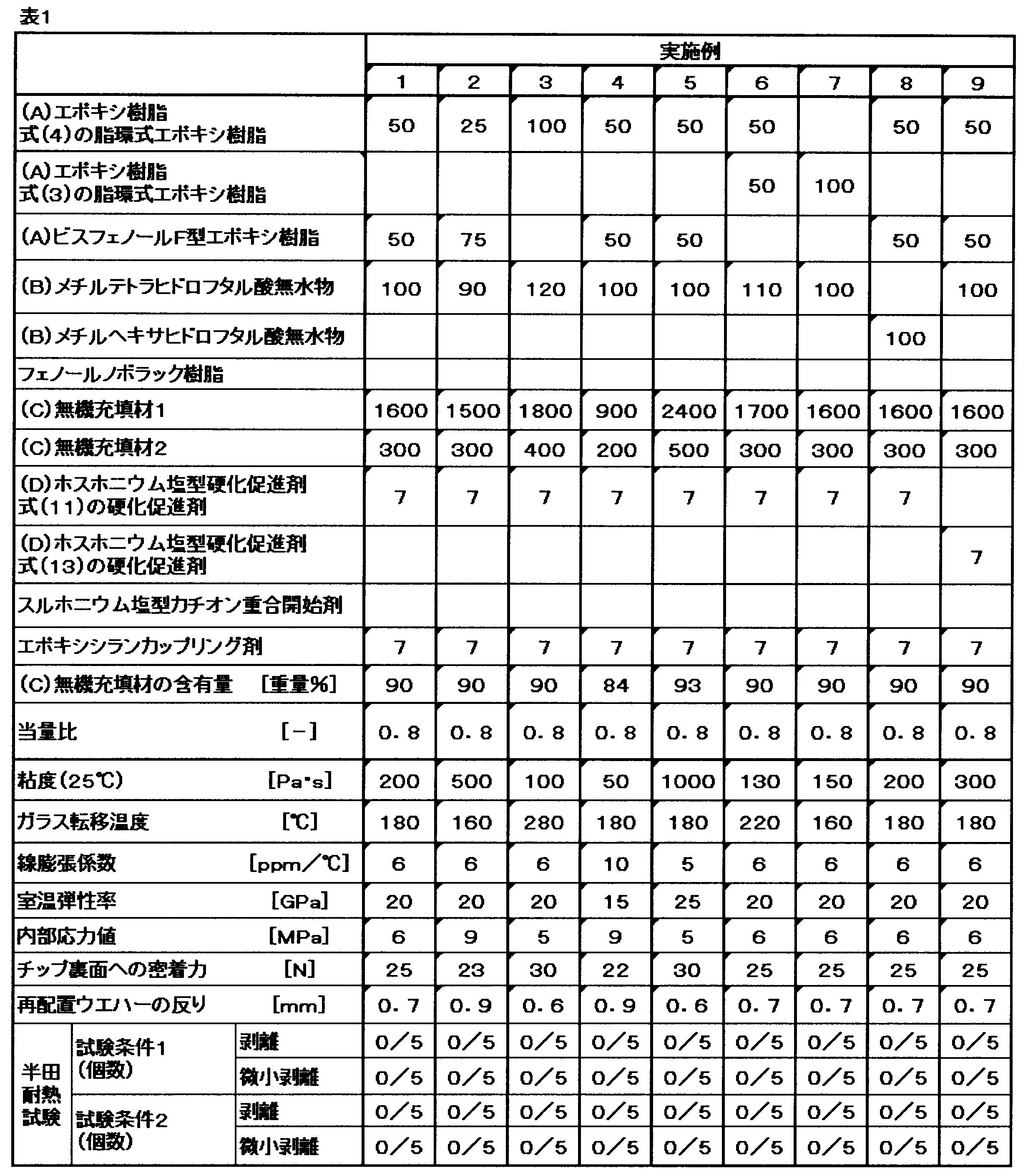

上記表において、当量比は、エポキシ基のモル数とカルボキシル基のモル数の比を示す。
本発明により、液状樹脂封止材を用いて作製されたウエハーレベルパッケージ、とりわけ圧縮成形でウエハー状に形成されたウエハーレベル工程で製造される半導体装置において、反りが少なく吸着搬送が容易で生産性高い擬似ウエハーを提供する事が出来る。
Claims (9)
- シリコンウェハーと液状樹脂組成物の硬化物の2層状態において式(1)により得られる内部応力値(σ)が10MPa以下である液状樹脂組成物。

- 硬化物の粘弾性測定装置で測定したガラス転移温度Tmgが150℃以上350℃以下である請求項1に記載の液状樹脂組成物。
- 前記液状樹脂組成物が(A)エポキシ樹脂、(B)酸無水物、(C)無機充填材、及び(D)硬化促進剤を含有し、無機充填材が全液状樹脂組成物に対して60重量%以上95重量%以下含まれる請求項1又は2に記載の液状樹脂組成物。
- (A)エポキシ樹脂が脂環式エポキシ樹脂を含むものである請求項3に記載の液状樹脂組成物。
- 前記脂環式エポキシ樹脂が、下記式(2)で表される3,4,3’,4’-ジエポキシビシクロヘキシル化合物を含む請求項4に記載の液状樹脂組成物。
- 請求項1乃至請求項5のいずれか一項に記載の液状樹脂組成物を用いて、半導体チップを支持体に多数個配置し、封止して作製した再配置ウエハー。
- 請求項6に記載の再配置ウエハーにおいて、半導体チップを支持体に多数個配置したものを圧縮成形により、封止して作製された再配置ウエハー。
- 請求項6又は請求項7に記載の再配置ウエハーを個片化して作製した半導体パッケージ。
- 請求項1乃至請求項5のいずれか一項に記載の液状樹脂組成物を用いて作製される半導体パッケージの製造方法であって、半導体チップを支持体に多数個配置する工程、この上に前記液状樹脂組成物を塗布する工程、金型により成形する工程、を含む半導体パッケージの製造方法。
Applications Claiming Priority (2)
| Application Number | Priority Date | Filing Date | Title |
|---|---|---|---|
| JP2011-074586 | 2011-03-30 | ||
| JP2011074586A JP2012209453A (ja) | 2011-03-30 | 2011-03-30 | 液状樹脂組成物、半導体パッケージ、および半導体パッケージの製造方法 |
Publications (1)
| Publication Number | Publication Date |
|---|---|
| WO2012133384A1 true WO2012133384A1 (ja) | 2012-10-04 |
Family
ID=46931101
Family Applications (1)
| Application Number | Title | Priority Date | Filing Date |
|---|---|---|---|
| PCT/JP2012/057887 Ceased WO2012133384A1 (ja) | 2011-03-30 | 2012-03-27 | 液状樹脂組成物、半導体パッケージ、および半導体パッケージの製造方法 |
Country Status (3)
| Country | Link |
|---|---|
| JP (1) | JP2012209453A (ja) |
| TW (1) | TW201245260A (ja) |
| WO (1) | WO2012133384A1 (ja) |
Families Citing this family (11)
| Publication number | Priority date | Publication date | Assignee | Title |
|---|---|---|---|---|
| JP6474719B2 (ja) * | 2013-02-19 | 2019-02-27 | 株式会社ダイセル | 硬化性組成物及びその硬化物、光学部材、並びに光学装置 |
| WO2015046334A1 (ja) | 2013-09-27 | 2015-04-02 | 株式会社ダイセル | 半導体素子三次元実装用充填材 |
| JP6315170B2 (ja) | 2013-09-30 | 2018-04-25 | ナガセケムテックス株式会社 | 半導体封止用エポキシ樹脂組成物、半導体実装構造体、およびその製造方法 |
| KR20170018839A (ko) * | 2014-06-16 | 2017-02-20 | 아사히 가라스 가부시키가이샤 | 복합체 |
| JP2016012021A (ja) * | 2014-06-27 | 2016-01-21 | 富士フイルム株式会社 | 偏光板保護フィルム、偏光板、画像表示装置、及び偏光板保護フィルムの製造方法 |
| JP2016108367A (ja) * | 2014-12-02 | 2016-06-20 | 信越化学工業株式会社 | 半導体封止用樹脂組成物及び該樹脂組成物を用いた半導体封止方法 |
| JP6369405B2 (ja) | 2015-07-07 | 2018-08-08 | 信越化学工業株式会社 | 半導体封止用熱硬化性樹脂組成物 |
| JP6597471B2 (ja) | 2016-05-02 | 2019-10-30 | 信越化学工業株式会社 | 大面積の半導体素子搭載基材を封止する方法 |
| JP6224188B1 (ja) | 2016-08-08 | 2017-11-01 | 太陽インキ製造株式会社 | 半導体封止材 |
| JP6520872B2 (ja) | 2016-09-01 | 2019-05-29 | 信越化学工業株式会社 | 半導体封止用熱硬化性樹脂組成物 |
| WO2026004928A1 (ja) * | 2024-06-28 | 2026-01-02 | 株式会社レゾナック | 硬化性樹脂組成物及び構造体 |
Citations (1)
| Publication number | Priority date | Publication date | Assignee | Title |
|---|---|---|---|---|
| JPH1030050A (ja) * | 1996-07-15 | 1998-02-03 | Hitachi Ltd | 半導体封止用熱硬化性樹脂組成物、それを用いた半導体装置およびその製法 |
-
2011
- 2011-03-30 JP JP2011074586A patent/JP2012209453A/ja not_active Withdrawn
-
2012
- 2012-03-26 TW TW101110398A patent/TW201245260A/zh unknown
- 2012-03-27 WO PCT/JP2012/057887 patent/WO2012133384A1/ja not_active Ceased
Patent Citations (1)
| Publication number | Priority date | Publication date | Assignee | Title |
|---|---|---|---|---|
| JPH1030050A (ja) * | 1996-07-15 | 1998-02-03 | Hitachi Ltd | 半導体封止用熱硬化性樹脂組成物、それを用いた半導体装置およびその製法 |
Also Published As
| Publication number | Publication date |
|---|---|
| TW201245260A (en) | 2012-11-16 |
| JP2012209453A (ja) | 2012-10-25 |
Similar Documents
| Publication | Publication Date | Title |
|---|---|---|
| JP2012209453A (ja) | 液状樹脂組成物、半導体パッケージ、および半導体パッケージの製造方法 | |
| JP2011195742A (ja) | 液状樹脂組成物、半導体パッケージ、および半導体パッケージの製造方法 | |
| JP4935670B2 (ja) | 半導体装置、並びにバッファーコート用樹脂組成物、ダイボンド用樹脂組成物、及び封止用樹脂組成物 | |
| JP6090614B2 (ja) | 半導体封止用液状エポキシ樹脂組成物及び樹脂封止半導体装置 | |
| JP7238271B2 (ja) | 電子装置、及び電子装置の製造方法 | |
| TWI667737B (zh) | Semiconductor device manufacturing method and semiconductor device | |
| JP2013010940A (ja) | 液状樹脂組成物およびそれを用いた半導体装置 | |
| JP2012227441A (ja) | 半導体装置の製造方法および半導体装置 | |
| TW202103277A (zh) | 半導體封裝 | |
| TW201841268A (zh) | 半導體裝置的製造方法、用於模具底部填充的感光性樹脂組成物以及半導體裝置 | |
| JP2020107767A (ja) | 封止用樹脂組成物、中空パッケージおよびその製造方法 | |
| TWI834787B (zh) | 空心封裝體及其製造方法 | |
| JP2017212416A (ja) | 電子装置の製造方法 | |
| JP2012129326A (ja) | 電子装置の製造方法および電子装置パッケージの製造方法 | |
| JP6627390B2 (ja) | 感光性封止樹脂組成物、それを用いた半導体装置の製造方法及び半導体装置 | |
| TWI768111B (zh) | 負型感光性樹脂組成物、半導體裝置及電子機器 | |
| TW202348699A (zh) | 表面改質材料用樹脂組成物 | |
| JP5157980B2 (ja) | 半導体素子封止体の製造方法および半導体パッケージの製造方法 | |
| TW202020565A (zh) | 負型感光性樹脂組成物、及使用其之半導體裝置 | |
| JP2011116843A (ja) | 液状封止用樹脂組成物およびそれを用いた半導体装置 | |
| JP5120305B2 (ja) | 半導体素子封止体の製造方法および半導体パッケージの製造方法 | |
| WO2020255749A1 (ja) | 封止用組成物、半導体装置及び半導体装置の製造方法 | |
| JP5557158B2 (ja) | フリップチップ接続用アンダーフィル剤、及びそれを用いる半導体装置の製造方法 | |
| JP2011052160A (ja) | 液状封止用樹脂組成物、半導体パッケージ、および半導体パッケージの製造方法 | |
| WO2012070612A1 (ja) | 電子装置の製造方法、電子装置、電子装置パッケージの製造方法、電子装置パッケージ、および半導体装置の製造方法 |
Legal Events
| Date | Code | Title | Description |
|---|---|---|---|
| 121 | Ep: the epo has been informed by wipo that ep was designated in this application |
Ref document number: 12764127 Country of ref document: EP Kind code of ref document: A1 |
|
| NENP | Non-entry into the national phase |
Ref country code: DE |
|
| 122 | Ep: pct application non-entry in european phase |
Ref document number: 12764127 Country of ref document: EP Kind code of ref document: A1 |