WO2012132389A1 - バックライトシステム - Google Patents
バックライトシステム Download PDFInfo
- Publication number
- WO2012132389A1 WO2012132389A1 PCT/JP2012/002077 JP2012002077W WO2012132389A1 WO 2012132389 A1 WO2012132389 A1 WO 2012132389A1 JP 2012002077 W JP2012002077 W JP 2012002077W WO 2012132389 A1 WO2012132389 A1 WO 2012132389A1
- Authority
- WO
- WIPO (PCT)
- Prior art keywords
- backlight
- drive signal
- duty ratio
- driver
- brightness
- Prior art date
- Legal status (The legal status is an assumption and is not a legal conclusion. Google has not performed a legal analysis and makes no representation as to the accuracy of the status listed.)
- Ceased
Links
Images




Classifications
-
- H—ELECTRICITY
- H05—ELECTRIC TECHNIQUES NOT OTHERWISE PROVIDED FOR
- H05B—ELECTRIC HEATING; ELECTRIC LIGHT SOURCES NOT OTHERWISE PROVIDED FOR; CIRCUIT ARRANGEMENTS FOR ELECTRIC LIGHT SOURCES, IN GENERAL
- H05B45/00—Circuit arrangements for operating light-emitting diodes [LED]
- H05B45/20—Controlling the colour of the light
-
- H—ELECTRICITY
- H05—ELECTRIC TECHNIQUES NOT OTHERWISE PROVIDED FOR
- H05B—ELECTRIC HEATING; ELECTRIC LIGHT SOURCES NOT OTHERWISE PROVIDED FOR; CIRCUIT ARRANGEMENTS FOR ELECTRIC LIGHT SOURCES, IN GENERAL
- H05B45/00—Circuit arrangements for operating light-emitting diodes [LED]
- H05B45/30—Driver circuits
- H05B45/32—Pulse-control circuits
- H05B45/325—Pulse-width modulation [PWM]
-
- H—ELECTRICITY
- H05—ELECTRIC TECHNIQUES NOT OTHERWISE PROVIDED FOR
- H05B—ELECTRIC HEATING; ELECTRIC LIGHT SOURCES NOT OTHERWISE PROVIDED FOR; CIRCUIT ARRANGEMENTS FOR ELECTRIC LIGHT SOURCES, IN GENERAL
- H05B45/00—Circuit arrangements for operating light-emitting diodes [LED]
- H05B45/30—Driver circuits
- H05B45/37—Converter circuits
- H05B45/3725—Switched mode power supply [SMPS]
- H05B45/38—Switched mode power supply [SMPS] using boost topology
-
- G—PHYSICS
- G02—OPTICS
- G02F—OPTICAL DEVICES OR ARRANGEMENTS FOR THE CONTROL OF LIGHT BY MODIFICATION OF THE OPTICAL PROPERTIES OF THE MEDIA OF THE ELEMENTS INVOLVED THEREIN; NON-LINEAR OPTICS; FREQUENCY-CHANGING OF LIGHT; OPTICAL LOGIC ELEMENTS; OPTICAL ANALOGUE/DIGITAL CONVERTERS
- G02F1/00—Devices or arrangements for the control of the intensity, colour, phase, polarisation or direction of light arriving from an independent light source, e.g. switching, gating or modulating; Non-linear optics
- G02F1/01—Devices or arrangements for the control of the intensity, colour, phase, polarisation or direction of light arriving from an independent light source, e.g. switching, gating or modulating; Non-linear optics for the control of the intensity, phase, polarisation or colour
- G02F1/13—Devices or arrangements for the control of the intensity, colour, phase, polarisation or direction of light arriving from an independent light source, e.g. switching, gating or modulating; Non-linear optics for the control of the intensity, phase, polarisation or colour based on liquid crystals, e.g. single liquid crystal display cells
- G02F1/133—Constructional arrangements; Operation of liquid crystal cells; Circuit arrangements
- G02F1/1333—Constructional arrangements; Manufacturing methods
- G02F1/1335—Structural association of cells with optical devices, e.g. polarisers or reflectors
- G02F1/1336—Illuminating devices
- G02F1/133601—Illuminating devices for spatial active dimming
-
- G—PHYSICS
- G02—OPTICS
- G02F—OPTICAL DEVICES OR ARRANGEMENTS FOR THE CONTROL OF LIGHT BY MODIFICATION OF THE OPTICAL PROPERTIES OF THE MEDIA OF THE ELEMENTS INVOLVED THEREIN; NON-LINEAR OPTICS; FREQUENCY-CHANGING OF LIGHT; OPTICAL LOGIC ELEMENTS; OPTICAL ANALOGUE/DIGITAL CONVERTERS
- G02F2201/00—Constructional arrangements not provided for in groups G02F1/00 - G02F7/00
- G02F2201/58—Arrangements comprising a monitoring photodetector
-
- G—PHYSICS
- G09—EDUCATION; CRYPTOGRAPHY; DISPLAY; ADVERTISING; SEALS
- G09G—ARRANGEMENTS OR CIRCUITS FOR CONTROL OF INDICATING DEVICES USING STATIC MEANS TO PRESENT VARIABLE INFORMATION
- G09G2310/00—Command of the display device
- G09G2310/02—Addressing, scanning or driving the display screen or processing steps related thereto
- G09G2310/0237—Switching ON and OFF the backlight within one frame
-
- G—PHYSICS
- G09—EDUCATION; CRYPTOGRAPHY; DISPLAY; ADVERTISING; SEALS
- G09G—ARRANGEMENTS OR CIRCUITS FOR CONTROL OF INDICATING DEVICES USING STATIC MEANS TO PRESENT VARIABLE INFORMATION
- G09G2320/00—Control of display operating conditions
- G09G2320/02—Improving the quality of display appearance
- G09G2320/0233—Improving the luminance or brightness uniformity across the screen
-
- G—PHYSICS
- G09—EDUCATION; CRYPTOGRAPHY; DISPLAY; ADVERTISING; SEALS
- G09G—ARRANGEMENTS OR CIRCUITS FOR CONTROL OF INDICATING DEVICES USING STATIC MEANS TO PRESENT VARIABLE INFORMATION
- G09G2320/00—Control of display operating conditions
- G09G2320/06—Adjustment of display parameters
- G09G2320/0626—Adjustment of display parameters for control of overall brightness
- G09G2320/064—Adjustment of display parameters for control of overall brightness by time modulation of the brightness of the illumination source
-
- G—PHYSICS
- G09—EDUCATION; CRYPTOGRAPHY; DISPLAY; ADVERTISING; SEALS
- G09G—ARRANGEMENTS OR CIRCUITS FOR CONTROL OF INDICATING DEVICES USING STATIC MEANS TO PRESENT VARIABLE INFORMATION
- G09G3/00—Control arrangements or circuits, of interest only in connection with visual indicators other than cathode-ray tubes
- G09G3/20—Control arrangements or circuits, of interest only in connection with visual indicators other than cathode-ray tubes for presentation of an assembly of a number of characters, e.g. a page, by composing the assembly by combination of individual elements arranged in a matrix no fixed position being assigned to or needed to be assigned to the individual characters or partial characters
- G09G3/34—Control arrangements or circuits, of interest only in connection with visual indicators other than cathode-ray tubes for presentation of an assembly of a number of characters, e.g. a page, by composing the assembly by combination of individual elements arranged in a matrix no fixed position being assigned to or needed to be assigned to the individual characters or partial characters by control of light from an independent source
- G09G3/3406—Control of illumination source
Definitions
- the present disclosure relates to a system for driving a backlight used in a liquid crystal display panel or the like.
- a display panel such as a liquid crystal display (LCD) panel is often irradiated with light from a backlight from the back.
- a light emitting diode LED
- the LED is often turned on and off. It is turned on and off at a sufficiently fast frequency (eg, on the order of 50 Hz) so that flicker is not perceived by the human eye.
- the current through the LED can be pulse width modulated (PWM).
- PWM pulse width modulated
- the LCD panel has a liquid crystal layer, a semiconductor layer, and the like.
- the writing voltage to the liquid crystal changes. This is because the characteristics of the thin film transistor (TFT) LCD change due to light irradiation on the semiconductor layer.
- TFT thin film transistor
- the LED when light is applied to the semiconductor of the LCD panel by the backlight LED, the writing voltage decreases. Therefore, when the LED is on, the display on the LCD panel may appear darker to the human eye than when the LED is off.
- an object of the present invention is to provide a backlight system that can reduce unevenness in luminance of a display panel.
- an apparatus for driving a backlight that illuminates a display panel has a control terminal, and switches a current flowing through the backlight based on a drive signal applied to the control terminal.
- a switching element a driver that outputs to the control terminal as the drive signal having a duty ratio determined according to the brightness of the backlight; and a controller that controls a time interval of a pulse group in the drive signal.
- an apparatus for driving a backlight for illuminating a display panel has a control terminal, and switches a current flowing through the backlight based on a drive signal applied to the control terminal.
- a switching element that outputs, a driver that outputs to the control terminal as the drive signal having a target duty ratio determined according to the brightness of the backlight, and a time average of instantaneous duty ratios of pulses in the drive signal
- a controller that changes the instantaneous duty ratio while being substantially equal to the target duty ratio.
- FIG. 1 is a diagram illustrating a liquid crystal display system using a backlight system according to an exemplary embodiment of the present invention.
- FIG. 2 is a diagram illustrating a backlight system according to an exemplary embodiment of the present invention.
- FIG. 3 is a diagram illustrating a drive signal and a modulation signal.
- FIG. 4 is a diagram illustrating a drive signal and a modulation signal.
- FIG. 5 illustrates in more detail a backlight system according to an exemplary embodiment of the present invention.
- FIG. 6 is a diagram illustrating a backlight system according to an exemplary embodiment of the present invention.
- FIG. 7 is a diagram illustrating a drive signal and a modulation signal.
- FIG. 8 is a diagram illustrating a drive signal and a modulation signal.
- FIG. 1 is a diagram illustrating a liquid crystal display (LCD) system 100 using a backlight system according to an exemplary embodiment of the present invention.
- the LCD system 100 is used for a display monitor for a television or a personal computer.
- the LCD system 100 includes an LCD panel 110, a backlight 150, and the like.
- the backlight 150 is provided on the back surface of the LCD panel 110 when viewed from the user of the LCD system 100.
- the backlight 150 irradiates the back surface of the LCD panel 110 with light.
- the light from the backlight 150 passes through the LCD panel 110 and reaches the user. With such a configuration, the user can view an image on the LCD panel 110.
- the backlight 150 is typically implemented with a white light emitting diode (LED).
- LCD system 100 uses LCD panel 110 as the display panel, but other suitable types of display panels may be used. Examples of such display panels include plasma displays and organic EL displays.
- the LCD panel 110 has a plurality of pixels (for example, 1920 ⁇ 1080 pixels).
- FIG. 1 shows only one pixel 112 as a representative of the plurality of pixels.
- the pixel 112 typically includes a thin film transistor (TFT) 114 and a liquid crystal layer 116.
- TFT thin film transistor
- the light transmittance of the liquid crystal layer 116 changes with brightness according to the voltage applied to the gate and source of the TFT 114. Therefore, an image can be displayed on the LCD panel 110 if an appropriate voltage is applied to the pixel by the gate driver 106 and the source driver 108.
- the display signal processor 104 receives the video signal at the input node 102, generates a signal corresponding to the position of the pixel and the color of the pixel, and outputs the signal to the gate driver 106 and the source driver 108.
- the gate driver 106 drives the gate of the pixel based on the generated signal.
- the source driver 108 drives the source of the pixel based on the generated signal.
- the backlight 150 is driven by a driver 160.
- the backlight 150 irradiates the LCD panel 110 with light of appropriate brightness based on the brightness of the image displayed on the LCD panel 110, the ambient brightness, and the like. In other words, the backlight 150 does not always irradiate the LCD panel 110 with light having a constant brightness.
- the driver 160 receives a signal necessary for controlling the illumination of light at the input node 162, and controls the driving of the backlight 150 based on the received signal.
- a signal used for controlling the light irradiation of the backlight 150 for example, there is a signal indicating the brightness of the pixel 112.
- FIG. 2 is a diagram illustrating a backlight system 200 according to an exemplary embodiment of the present invention.
- the backlight system 200 corresponds to the backlight 150 and the driver 160 in the LCD system 100 of FIG.
- the backlight system 200 includes a switching element 210, a driver 220, a controller 230, and a backlight 240.
- the backlight system 200 may not include the backlight 240, and in that case, the backlight system 200 may be referred to as a backlight driver system or a backlight driver.
- the backlight 240 is typically realized by a plurality of LEDs 242.
- the LED 242 is preferably a white LED. In FIG. 2, all the LEDs 242 are connected in series, but the present invention is not limited to this. For example, LED groups connected in series may be connected in parallel.
- the power supply node 250 receives a positive voltage (for example, on the order of 20 to 30 V) with respect to the ground 252 and passes a forward current to the backlight 240 through the switching element 210.
- the switching element 210 has a control terminal 212 and non-control terminals 214 and 216.
- a voltage applied to the control terminal 212 or a current flowing through the control terminal 212 controls conduction of the non-control terminals 214 and 216.
- the switching element 210 is a field effect transistor (FET)
- the control terminal 212 is a gate
- the non-control terminals 214 and 216 are a drain and a source (or vice versa).
- the switching element 210 is a bipolar transistor
- the control terminal 212 is a base
- the non-control terminals 214 and 216 are a collector and an emitter (or vice versa).
- the switching element 210 switches the current flowing through the backlight 240 based on the drive signal PWM applied to the control terminal 212.
- the driver 220 receives the lightness signal Cv and the modulation signal Cmod, and outputs a drive signal PWM to the control terminal 212 based on these input signals.
- the lightness signal Cv may be a signal representing the lightness of the pixel 112, for example.
- the lightness signal Cv is generated by the source driver 108, for example.
- the brightness of the backlight 240 is preferably changed (eg, proportionally) based on the brightness of the pixel 112. In other words, the brightness of the backlight 240 is preferably determined based on the voltage of the lightness signal Cv (eg, in proportion).
- the brightness of a single pixel 112 reflects the brightness of the entire LCD panel 110.
- the brightness of the LCD panel 110 may be represented by, for example, an average value of a plurality of pixel groups.
- the brightness of the LCD panel 110 may be represented by the brightness of multiple areas.
- the drive signal PWM has a duty ratio determined according to the brightness of the backlight 240. For example, when the backlight 240 is to be lit brightly, the duty ratio of the drive signal PWM is large (for example, 80%). Conversely, when the backlight 240 is to be lit darkly, the duty ratio of the drive signal PWM is small. (Eg 20%).
- the controller 230 outputs a modulation signal Cmod for controlling the time interval of the pulse group in the drive signal PWM to the driver 220.
- the driver 220 generates a drive signal PWM having a duty ratio determined based on the lightness signal Cv. Therefore, if the brightness of the pixel 112 is constant, the brightness signal Cv is also constant, and the duty ratio of the drive signal PWM is kept constant.
- the driver 220 controls the time interval of the pulse group in the drive signal PWM based on the modulation signal Cmod. This time interval control is independent of the duty ratio control based on the lightness signal Cv.
- FIG. 3 is a diagram showing the drive signal PWM and the modulation signal Cmod.
- the horizontal axis represents time, and the vertical axis represents the voltage of the drive signal PWM and the time interval ti represented by the modulation signal Cmod.
- the duty ratio of the drive signal PWM is also constant. Therefore, as shown in FIG. 3, after time t1, the duty ratio of the drive signal PWM is constant at 50%, for example.
- the driver 220 controls the time interval of the pulse group in the drive signal PWM based on the modulation signal Cmod.
- the modulation signal Cmod switches between the time intervals ti1 and ti2.
- the time interval of the pulse group in the drive signal PWM is ti1
- the time interval of the pulse group in the drive signal PWM is ti2.
- the modulation signal Cmod alternately takes two values of the time intervals ti1 and ti2.
- the driver 220 switches the time interval between two adjacent pulse groups in the drive signal PWM between the time intervals ti1 and ti2 based on the modulation signal Cmod.
- the controller 230 controls the driver 220 so that the pulse group in the drive signal PWM alternately repeats the first time interval ti1 and the second time interval ti2.
- the controller 230 controls the driver 220 so that the pulse group in the drive signal PWM repeats a pattern including at least one first time interval ti1 and at least one second time interval ti2. For example, assume that a certain pattern is ⁇ ti1, ti2, ti2 ⁇ . At this time, the controller 230 controls the driver 220 so that the pulse group in the drive signal PWM repeats this pattern. That is, the controller 230 controls the driver 220 so that the time intervals of the pulse groups in the drive signal PWM have ti1, ti2, ti2, ti1, ti2, ti2,. With such a configuration, luminance unevenness can be further reduced.
- FIG. 4 is a diagram showing the drive signal PWM and the modulation signal Cmod.
- the horizontal axis represents time, and the vertical axis represents the voltage of the drive signal PWM and the time interval ti represented by the modulation signal Cmod.
- the duty ratio of the drive signal PWM is also constant. Therefore, as shown in FIG. 4, after time t1, the duty ratio of the drive signal PWM is constant at 50%, for example.
- the driver 220 controls the time interval of the pulse group in the drive signal PWM based on the modulation signal Cmod.
- the modulation signal Cmod switches substantially randomly within the time interval ti1 to ti10. For example, in the period t1 to t2, the time interval of the pulse group in the drive signal PWM is ti10, but in the period t2 to t3, the time interval of the pulse group in the drive signal PWM is ti2.
- the modulation signal Cmod has values of time intervals ti6, ti8, ti4, ti9, ti1, ti5, respectively.
- the time intervals ti1 to ti10 are substantially random values.
- the driver 220 randomly switches the time interval between two adjacent pulse groups in the drive signal PWM within the time interval ti1 to ti10 based on the modulation signal Cmod. As a result, even when the frequency of the drive signal PWM is close to the frame frequency of the LCD panel 110, the luminance unevenness of the display panel is hardly recognized. This is because the boundary of luminance unevenness moves on the display panel by changing the time interval of the pulse group of the drive signal PWM.
- the controller 230 controls the driver 220 so that the pulse group has a plurality of time intervals substantially randomly. More specifically, the controller 230 controls the driver 220 so that the pulse group has time intervals ti1 to ti10 and the like substantially randomly. Such a configuration can further reduce luminance unevenness as compared with the above-described example in which the time interval ti is regularly changed.
- FIG. 5 is a diagram illustrating the backlight system 500 according to an exemplary embodiment of the present invention in more detail.
- the backlight system 500 includes a step-up chopper 510.
- the step-up chopper 510 includes an FET 512, an inductor 514, a diode 516, and a capacitor 518. Therefore, the FET 512 corresponds to the switching element 210.
- the switching efficiency can be improved as compared with a bipolar transistor or the like.
- the backlight system 500 can supply a voltage higher than the voltage applied to the power supply node 250 to the LED 240 by using the step-up chopper 510. This allows low voltage operation of the backlight system 500.
- FIG. 6 is a diagram illustrating a backlight system 600 according to an exemplary embodiment of the present invention.
- the backlight system 600 corresponds to the backlight 150 and the driver 160 in the LCD system 100 of FIG.
- the backlight system 600 includes a switching element 210, a driver 620, a controller 630, and a backlight 240.
- the backlight system 600 may not include the backlight 240, in which case it may be referred to as a backlight driver system or a backlight driver.
- the switching element 210, the backlight 240, the power supply node 250, and the ground 252 shown in FIG. 6 are the same or similar elements as those shown in FIG.
- the brightness signal Cv may be a signal representing the brightness of the pixel 112, for example.
- the lightness signal Cv is generated by the source driver 108, for example.
- the brightness of the backlight 240 is preferably changed (eg, proportionally) based on the brightness of the pixel 112. In other words, the brightness of the backlight 240 is preferably determined based on the voltage of the lightness signal Cv (eg, in proportion).
- the drive signal PWM has a duty ratio determined according to the brightness of the backlight 240. For example, when the backlight 240 is to be lit brightly, the duty ratio of the drive signal PWM is large (for example, 80%). Conversely, when the backlight 240 is to be lit darkly, the duty ratio of the drive signal PWM is small. (Eg 20%).
- the controller 630 first determines the target duty ratio dt0 based on the brightness signal Cv representing the desired brightness of the backlight 240. Therefore, the target duty ratio dt0 corresponds to the lightness signal Cv representing the desired brightness of the backlight 240.
- the controller 630 generates a modulation signal Cmod whose time average of the instantaneous duty ratio is equal to the target duty ratio dt0 and changes with time, and outputs it to the driver 620.
- the driver 620 receives the modulation signal Cmod and outputs a drive signal PWM to the control terminal 212 based on the modulation signal Cmod.
- the driver 620 generates a drive signal PWM whose instantaneous duty ratio changes based on the modulation signal Cmod.
- the time average of the instantaneous duty ratio of the pulses in the drive signal PWM is equal to the target duty ratio dt0. Therefore, if the brightness of the pixel 112 is constant, the voltage of the brightness signal Cv is also constant, and thus the target duty ratio dt0 is also constant.
- the target duty ratio dt0 When the brightness of the pixel 112 increases, the voltage of the brightness signal Cv also increases, and thus the target duty ratio dt0 also increases.
- the brightness of the pixel 112 decreases, the voltage of the brightness signal Cv also decreases, and therefore the target duty ratio dt0 also decreases.
- the brightness of the pixel 112 is assumed to be constant in the following description.
- FIG. 7 is a diagram showing the drive signal PWM and the modulation signal Cmod.
- the horizontal axis represents time, and the vertical axis represents the voltage of the drive signal PWM and the duty ratio (%) represented by the modulation signal Cmod.
- the time average of the instantaneous duty ratio of the pulses in the drive signal PWM is equal to the target duty ratio dt0 (50% in FIG. 7).
- the controller 630 changes the instantaneous duty ratio with a predetermined width while making the time average of the instantaneous duty ratio of the drive signal PWM equal to the target duty ratio dt0.
- the controller 630 has a group of pulses in the drive signal PWM substantially regularly having a first duty ratio (40% in FIG. 7) and a second duty ratio (60% in FIG. 7).
- the driver 620 is controlled.
- the modulation signal Cmod switches between a duty ratio of 40% and 60%.
- the instantaneous duty ratio of the drive signal PWM is 40% in the period t1 to t2, but the instantaneous duty ratio of the drive signal PWM is 60% in the period t2 to t3.
- the modulation signal Cmod alternately takes two values of an instantaneous duty ratio of 40% and 60%.
- the driver 620 Based on the modulation signal Cmod, the driver 620 makes the time average of the instantaneous duty ratios of the pulses in the drive signal PWM substantially equal to the target duty ratio dt0 (50% in FIG. 7), while the drive signal PWM Change the instantaneous duty ratio.
- the instantaneous duty ratio of the drive signal PWM is switched between 40% and 60%.
- the controller 630 typically controls the driver 620 so that the pulse group in the drive signal PWM alternately repeats the first duty ratio and the second duty ratio. With such a configuration, it is possible to reduce luminance unevenness with a simple configuration.
- the controller 630 controls the driver 620 so that the pulse group in the drive signal PWM repeats a pattern including at least one first duty ratio dt1 and at least one second time interval dt2. For example, it is assumed that a certain pattern is ⁇ dt1, dt2, dt2 ⁇ and the target duty ratio dt0. At this time, the controller 630 controls the driver 620 so that the pulse group in the drive signal PWM repeats this pattern. That is, the controller 630 controls the driver 620 so that the duty ratio of the pulse group in the drive signal PWM has dt1, dt2, dt2, dt1, dt2, dt2,. With such a configuration, luminance unevenness can be further reduced.
- FIG. 8 is a diagram showing the drive signal PWM and the modulation signal Cmod.
- the horizontal axis represents time, and the vertical axis represents the voltage of the drive signal PWM and the duty ratio (%) represented by the modulation signal Cmod.
- the time average of the instantaneous duty ratio of the pulses in the drive signal PWM is equal to the target duty ratio dt0 (50% in FIG. 8).
- the controller 630 changes the instantaneous duty ratio with a predetermined width while making the time average of the instantaneous duty ratio of the drive signal PWM equal to the target duty ratio dt0.
- the controller 630 controls the driver 620 so that the pulses in the drive signal PWM have a plurality of duty ratios substantially randomly.
- the duty ratio represented by the modulation signal Cmod is substantially randomly selected from values in the range of 15% to 85% duty ratio.
- the instantaneous duty ratio of the drive signal PWM is 70%
- the instantaneous duty ratio of the drive signal PWM is 15%
- the modulation signal Cmod takes values of instantaneous duty ratios of 60%, 45%, and 85%, respectively.
- the modulation signal Cmod takes a substantially random value within the range of the instantaneous duty ratio of 15% to 85%.
- the driver 620 Based on the modulation signal Cmod, the driver 620 makes the time average of the instantaneous duty ratios of the pulses in the drive signal PWM substantially equal to the target duty ratio dt0 (50% in FIG. 8), while the drive signal PWM The instantaneous duty ratio is changed substantially randomly as described above. As a result, even when the frequency of the drive signal PWM is close to the frame frequency of the LCD panel 110, the luminance unevenness of the display panel is hardly recognized. This is because the boundary of luminance unevenness moves on the display panel by changing the instantaneous duty ratio of the pulse group of the drive signal PWM.
- the controller 630 controls the driver 620 so that the pulse group has a plurality of time intervals substantially randomly. More specifically, the controller 630 controls the driver 620 so that the instantaneous duty ratio of the drive signal PWM takes a substantially random value within the range of 15% to 85%. Such a configuration can further reduce luminance unevenness as compared with the above-described example in which the duty ratio is regularly changed.
- the backlight system 600 may use the step-up chopper 510 as described with reference to FIG. By using the FET 512 as the switching element 210, the switching efficiency can be improved as compared with a bipolar transistor or the like.
- the backlight system 600 can supply a voltage higher than the voltage applied to the power supply node 250 to the LED 240 by using the step-up chopper 510. This allows low voltage operation of the backlight system 600.
- controllers 230 and 630 generate substantially random values, i.e., time intervals and duty ratios, respectively. Such a random value may be realized in hardware, software, or a combination thereof.
- the “substantially random value” in the present specification does not need to be completely random, but may have variations enough to be regarded as random. Therefore, the controllers 230 and 630 may use a hardware random number generator, for example, and may generate pseudo random numbers by software. Alternatively, the controllers 230 and 630 may sequentially read the random number sequence stored in the memory.
- various functions can be realized as individual elements. Conversely, a plurality of functions may be realized as a single element. For example, a plurality of functions may be realized as a single circuit element such as a single semiconductor chip or a single hybrid integrated circuit. It may be realized above.
- Backlight system 210 Switching element 212 Control terminal 214, 216 Non-control terminal 220 Driver 230 Controller 240 Backlight 242 Light emitting diode 250 Power supply node 252 Ground Cv Lightness signal Cmod Modulation signal PWM Drive signal
Landscapes
- Liquid Crystal (AREA)
- Control Of Indicators Other Than Cathode Ray Tubes (AREA)
Abstract
ディスプレイパネルの輝度ムラを低減することができるバックライトシステムを提供する。ディスプレイパネルを照射するバックライトを駆動する装置であって、制御端子を有し、制御端子に印加される駆動信号に基づいてバックライトに流れる電流をスイッチングするスイッチング素子と、バックライトの明るさに応じて決定されるデューティ比を有する駆動信号として制御端子に出力するドライバと、駆動信号中のパルス群の時間間隔を制御するコントローラとを備える。
Description
本開示は、液晶ディスプレイパネルなどに用いられるバックライトを駆動するシステムに関する。
液晶ディスプレイ(LCD)パネルなどのディスプレイパネルは、その背面からバックライトによる光を照射されることが多い。バックライトとしては、典型的には発光ダイオード(LED)が用いられる。LEDは、常にオンされる代わりに、オン、オフされることが多い。ちらつきが人間の目で認識されないように、十分に速い周波数(例えば50Hzのオーダー)でオン、オフされる。バックライトの明るさを調整するために、LEDを流れる電流は、パルス幅変調(PWM)され得る。このようなPWMによる駆動は、例えば特許文献1に記載されている。
LCDパネルは、液晶層、半導体層などを有する。LCDパネルの半導体層へ光が照射されると、液晶への書き込み電圧が変化する。これは半導体層への光照射によって、薄膜トランジスタ(TFT)LCDの特性が変化することに起因する。例えば、バックライトのLEDによって光がLCDパネルの半導体へ照射されると、書き込み電圧が下がる。そのためLEDがオンであるときは、LEDがオフであるときに比べて、LCDパネルの表示が人間の目には暗く見えることがあり得る。
LEDを駆動するのに用いられるPWMの周波数が、LCDパネルのフレーム周波数に近いときは、LCDパネル上で例えば水平の帯状の輝度ムラとなって認識され得る。特に中間調のベタ領域が表示されると、そのような輝度ムラは目立ちやすい。ところが従来技術による装置では、このようなムラを低減することは困難であった。そこで、本発明の目的は、ディスプレイパネルの輝度ムラを低減することができるバックライトシステムを提供することにある。
本発明のある実施形態によれば、ディスプレイパネルを照射するバックライトを駆動する装置は、制御端子を有し、前記制御端子に印加される駆動信号に基づいて前記バックライトに流れる電流をスイッチングするスイッチング素子と、前記バックライトの明るさに応じて決定されるデューティ比を有する前記駆動信号として前記制御端子に出力するドライバと、前記駆動信号中のパルス群の時間間隔を制御するコントローラとを備える。
本発明の他の実施形態によれば、ディスプレイパネルを照射するバックライトを駆動する装置は、制御端子を有し、前記制御端子に印加される駆動信号に基づいて前記バックライトに流れる電流をスイッチングするスイッチング素子と、前記バックライトの明るさに応じて決定される目標デューティ比を有する前記駆動信号として前記制御端子に出力するドライバと、前記駆動信号中のパルス群の瞬時デューティ比の時間平均を、実質的に前記目標デューティ比に等しくしつつ、前記瞬時デューティ比を変化させるコントローラとを備える。
本発明によれば、ディスプレイパネルの輝度ムラを低減することができるバックライトシステムを提供できる。
本発明によるバックライトシステムの例示的実施形態について、図面を用いて詳細に説明する。図面において同一又は同様の構成要素は、同じ参照符号によって表される。
図1は、本発明の例示的実施形態によるバックライトシステムを用いる液晶ディスプレイ(LCD)システム100を示す図である。LCDシステム100は、テレビ、パーソナルコンピュータ用のディスプレイモニタなどに用いられる。LCDシステム100は、LCDパネル110、バックライト150などを有する。典型的には、LCDシステム100のユーザから見てLCDパネル110の背面にバックライト150は設けられる。
バックライト150は、LCDパネル110の背面に光を照射する。バックライト150からの光は、LCDパネル110を透過してユーザに届く。このような構成によりユーザはLCDパネル110上の画像を見ることができる。バックライト150は、典型的には白色発光ダイオード(LED)で実現される。LCDシステム100は、ディスプレイパネルとしてLCDパネル110を用いるが、他の適切なタイプのディスプレイパネルが用いられ得る。そのようなディスプレイパネルの例には、プラズマディスプレイ、有機ELディスプレイがある。
LCDパネル110は、複数の画素(例えば1920×1080画素)を有する。図1は、複数の画素の代表として1つの画素112だけを示す。画素112は、典型的には薄膜トランジスタ(TFT)114および液晶層116を含む。TFT 114のゲートおよびソースに印加される電圧に応じた明るさで液晶層116の光の透過率が変化する。よってゲートドライバ106およびソースドライバ108によって画素に適切な電圧を印加すれば、LCDパネル110に画像を表示することができる。
表示信号処理器104は、その入力ノード102で映像信号を受け取り、画素の位置および画素の色に応じた信号を生成し、ゲートドライバ106およびソースドライバ108に出力する。ゲートドライバ106は、生成された信号に基づいて画素のゲートを駆動する。ソースドライバ108は、生成された信号に基づいて画素のソースを駆動する。
バックライト150は、ドライバ160によって駆動される。典型的にはバックライト150は、LCDパネル110に表示される画像の明るさ、周囲の明るさなどに基づいて、適切な明るさの光をLCDパネル110に照射する。換言すれば、バックライト150は、常に一定の明るさの光をLCDパネル110に照射するのではない。ドライバ160は、その入力ノード162において光の照射を制御するのに必要な信号を受け取り、受け取られた信号に基づいてバックライト150の駆動を制御する。そのようなバックライト150の光の照射を制御するのに用いられる信号には、例えば画素112の明度を表す信号がある。
図2は、本発明の例示的実施形態によるバックライトシステム200を示す図である。バックライトシステム200は、図1のLCDシステム100のうちのバックライト150およびドライバ160に対応する。バックライトシステム200は、スイッチング素子210と、ドライバ220、コントローラ230、およびバックライト240を含む。バックライトシステム200は、バックライト240を含まなくてもよく、その場合、バックライトドライバシステム、またはバックライトドライバと呼ばれることもある。
バックライト240は、典型的には複数のLED 242で実現される。LED 242は好ましくは白色LEDである。図2では全てのLED 242が直列に接続されているが、これには限定されない。例えば直列に接続されたLED群を並列に接続してもよい。電源ノード250は、グラウンド252に対して正の電圧(例えば20~30Vのオーダー)を受け取り、スイッチング素子210を通してバックライト240に順方向電流を流す。
スイッチング素子210は、制御端子212、非制御端子214,216を有する。制御端子212に印加される電圧、または制御端子212を通って流れる電流が、非制御端子214,216の導通を制御する。スイッチング素子210が電界効果トランジスタ(FET)のときは、制御端子212はゲートであり、非制御端子214,216はドレイン,ソース(またはその逆)である。スイッチング素子210がバイポーラトランジスタのときは、制御端子212はベースであり、非制御端子214,216はコレクタ,エミッタ(またはその逆)である。スイッチング素子210は、制御端子212に印加される駆動信号PWMに基づいてバックライト240に流れる電流をスイッチングする。
ドライバ220は、明度信号Cvと、変調信号Cmodとを受け取り、これらの入力信号に基づいて駆動信号PWMを制御端子212に出力する。明度信号Cvは、例えば画素112の明度を表す信号であり得る。明度信号Cvは、例えばソースドライバ108によって生成される。バックライト240の明るさは、好ましくは、画素112の明度に基づいて(例えば比例して)変化される。換言すれば、バックライト240の明るさは、好ましくは、明度信号Cvの電圧に基づいて(例えば比例して)決定される。以下の説明では、簡単のため、単一の画素112の明度がLCDパネル110全体の明るさを反映すると仮定する。しかしLCDパネル110の明度は、複数の画素群の、例えば平均値によって表されてもよい。代替として、LCDパネル110の明度は、複数の領域の明度によって表されてもよい。
例えば画素112の明度が大きいときはバックライト240の明るさは高く、画素112の明度が小さいときはバックライト240の明るさは低い。これを実現するために、駆動信号PWMは、バックライト240の明るさに応じて決定されるデューティ比を有する。例えば、バックライト240が明るく点灯すべきときは、駆動信号PWMのデューティ比は大きくなり(例えば80%)、逆にバックライト240が暗く点灯すべきときは、駆動信号PWMのデューティ比は小さくなる(例えば20%)。
コントローラ230は、駆動信号PWM中のパルス群の時間間隔を制御する変調信号Cmodをドライバ220に出力する。ドライバ220は、明度信号Cvに基づいて決定されたデューティ比を有する駆動信号PWMを発生する。したがって画素112の明度が一定なら、明度信号Cvも一定であり、駆動信号PWMのデューティ比は一定に保たれる。一方でドライバ220は、変調信号Cmodに基づいて駆動信号PWM中のパルス群の時間間隔を制御する。この時間間隔制御は、明度信号Cvに基づくデューティ比制御とは独立している。
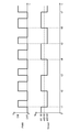
図3は、駆動信号PWMおよび変調信号Cmodを示す図である。横軸は時間を示し、縦軸は駆動信号PWMの電圧と、変調信号Cmodが表す時間間隔tiとを示す。画素112の明度が一定である、すなわち明度信号Cvが一定であると仮定すると、駆動信号PWMのデューティ比も一定である。したがって図3に示されるように、時刻t1以降、駆動信号PWMのデューティ比は例えば50%で一定である。
しかしドライバ220は、変調信号Cmodに基づいて駆動信号PWM中のパルス群の時間間隔を制御する。具体的には、変調信号Cmodは、時間間隔ti1およびti2の間で切り替わる。例えば、期間t1~t2では駆動信号PWM中のパルス群の時間間隔はti1であるが、期間t2~t3では駆動信号PWM中のパルス群の時間間隔はti2である。期間t3~t4,t4~t5,t5~t6などについても同様に、変調信号Cmodは、時間間隔ti1およびti2の2つの値を交互にとる。
ドライバ220は、変調信号Cmodに基づいて、駆動信号PWM中の2つの隣接するパルス群の時間間隔を時間間隔ti1およびti2の間で切り換える。その結果、駆動信号PWMの周波数がLCDパネル110のフレーム周波数に近い場合であっても、ディスプレイパネルの輝度ムラは認識されにくくなる。これは、駆動信号PWMのパルス群の時間間隔を変化させることによって、輝度ムラの境界がディスプレイパネル上で移動することによる。
図3に示されるように、典型的にはコントローラ230は、駆動信号PWM中のパルス群が第1時間間隔ti1および第2時間間隔ti2を交互に繰り返すように、ドライバ220を制御する。このような構成により、簡易な構成で輝度ムラを低減させることが可能である。
変形例として、コントローラ230は、駆動信号PWM中のパルス群が少なくとも1つの第1時間間隔ti1および少なくとも1つの第2時間間隔ti2を含むパターンを繰り返すように、ドライバ220を制御する。例えば、あるパターンが{ti1,ti2,ti2}であるとする。このときコントローラ230は、駆動信号PWM中のパルス群がこのパターンを繰り返すようにドライバ220を制御する。すなわちコントローラ230は、駆動信号PWM中のパルス群の時間間隔がti1,ti2,ti2,ti1,ti2,ti2,…を有するようにドライバ220を制御する。このような構成により、さらに輝度ムラを低減させることが可能である。
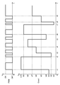
図4は、駆動信号PWMおよび変調信号Cmodを示す図である。横軸は時間を示し、縦軸は駆動信号PWMの電圧と、変調信号Cmodが表す時間間隔tiとを示す。画素112の明度が一定である、すなわち明度信号Cvが一定であると仮定すると、駆動信号PWMのデューティ比も一定である。したがって図4に示されるように、時刻t1以降、駆動信号PWMのデューティ比は例えば50%で一定である。
しかしドライバ220は、変調信号Cmodに基づいて駆動信号PWM中のパルス群の時間間隔を制御する。具体的には、変調信号Cmodは、時間間隔ti1~ti10の範囲内で実質的にランダムに切り替わる。例えば、期間t1~t2では駆動信号PWM中のパルス群の時間間隔はti10であるが、期間t2~t3では駆動信号PWM中のパルス群の時間間隔はti2である。同様に期間t3~t4,t4~t5,t5~t6,t6~t7,t7~t8,t8~t9については、変調信号Cmodは、それぞれ時間間隔ti6,ti8,ti4,ti9,ti1,ti5の値をとる。図4に示されるように、時間間隔ti1~ti10は実質的にランダムな値である。
ドライバ220は、変調信号Cmodに基づいて、駆動信号PWM中の2つの隣接するパルス群の時間間隔を時間間隔ti1~ti10の範囲内でランダムに切り換える。その結果、駆動信号PWMの周波数がLCDパネル110のフレーム周波数に近い場合であっても、ディスプレイパネルの輝度ムラは認識されにくくなる。これは、駆動信号PWMのパルス群の時間間隔を変化させることによって、輝度ムラの境界がディスプレイパネル上で移動することによる。
図4に示されるように、典型的にはコントローラ230は、パルス群が複数の時間間隔を実質的にランダムに有するように、ドライバ220を制御する。より具体的には、コントローラ230は、パルス群が時間間隔ti1~ti10などを実質的にランダムに有するように、ドライバ220を制御する。このような構成は、時間間隔tiを規則的に変化させる上述の例と比較して、輝度ムラをさらに低減させることが可能である。
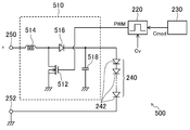
図5は、本発明の例示的実施形態によるバックライトシステム500をより詳細に示す図である。バックライトシステム500は、昇圧型チョッパ510を含む。昇圧型チョッパ510は、FET 512、インダクタ514、ダイオード516、およびキャパシタ518を含む。よってFET 512はスイッチング素子210に対応する。スイッチング素子210としてFET 512を利用することによって、バイポーラトランジスタなどと比較して、スイッチング効率が改善され得る。バックライトシステム500は、昇圧型チョッパ510を利用することによって、電源ノード250に印加される電圧より高い電圧をLED 240に供給することができる。これはバックライトシステム500の低電圧動作を可能にする。
図6は、本発明の例示的実施形態によるバックライトシステム600を示す図である。バックライトシステム600は、図1のLCDシステム100のうちのバックライト150およびドライバ160に対応する。バックライトシステム600は、スイッチング素子210と、ドライバ620、コントローラ630、およびバックライト240を含む。バックライトシステム600は、バックライト240を含まなくてもよく、その場合、バックライトドライバシステム、またはバックライトドライバと呼ばれることもある。図6に示されるスイッチング素子210、バックライト240、電源ノード250、およびグラウンド252は、図2に示されるものと同一または類似の要素である。
明度信号Cvは、例えば画素112の明度を表す信号であり得る。明度信号Cvは、例えばソースドライバ108によって生成される。バックライト240の明るさは、好ましくは、画素112の明度に基づいて(例えば比例して)変化される。換言すれば、バックライト240の明るさは、好ましくは、明度信号Cvの電圧に基づいて(例えば比例して)決定される。
例えば画素112の明度が大きいときはバックライト240の明るさは高く、画素112の明度が小さいときはバックライト240の明るさは低い。これを実現するために、駆動信号PWMは、バックライト240の明るさに応じて決定されるデューティ比を有する。例えば、バックライト240が明るく点灯すべきときは、駆動信号PWMのデューティ比は大きくなり(例えば80%)、逆にバックライト240が暗く点灯すべきときは、駆動信号PWMのデューティ比は小さくなる(例えば20%)。
コントローラ630は、バックライト240の所望の明るさを表す明度信号Cvに基づいて、目標デューティ比dt0をまず決定する。よって目標デューティ比dt0は、バックライト240の所望の明るさを表す明度信号Cvに対応する。コントローラ630は、瞬時デューティ比の時間平均がこの目標デューティ比dt0に等しく、かつ時間的に変化する変調信号Cmodを発生し、ドライバ620に出力する。
ドライバ620は、変調信号Cmodを受け取り、この変調信号Cmodに基づいて駆動信号PWMを制御端子212に出力する。ドライバ620は、変調信号Cmodに基づいて、瞬時デューティ比が変化する駆動信号PWMを発生する。しかし駆動信号PWM中のパルス群の瞬時デューティ比の時間平均は目標デューティ比dt0に等しい。したがって画素112の明度が一定なら、明度信号Cvの電圧も一定であり、よって目標デューティ比dt0も一定である。画素112の明度が増すとき、明度信号Cvの電圧も高くなり、よって目標デューティ比dt0も大きくなる。画素112の明度が減るとき、明度信号Cvの電圧も低くなり、よって目標デューティ比dt0も小さくなる。簡単のため、以下の記載では画素112の明度は一定であるとする。
図7は、駆動信号PWMおよび変調信号Cmodを示す図である。横軸は時間を示し、縦軸は駆動信号PWMの電圧と、変調信号Cmodが表すデューティ比(%)とを示す。
駆動信号PWM中のパルス群の瞬時デューティ比の時間平均は、目標デューティ比dt0(図7では50%)に等しい。コントローラ630は、駆動信号PWMの瞬時デューティ比の時間平均が目標デューティ比dt0に等しいようにしつつ、瞬時デューティ比を所定の幅で変化させる。ある実施形態によれば、コントローラ630は、駆動信号PWM中のパルス群が第1デューティ比(図7では40%)および第2デューティ比(図7では60%)を実質的に規則的に有するように、ドライバ620を制御する。換言すれば、変調信号Cmodは、デューティ比40%および60%の間で切り替わる。
例えば、期間t1~t2では駆動信号PWMの瞬時デューティ比は40%であるが、期間t2~t3では駆動信号PWMの瞬時デューティ比は60%である。期間t3~t4,t4~t5,t5~t6,t6~t7などについても同様に、変調信号Cmodは、瞬時デューティ比40%および60%の2つの値を交互にとる。
ドライバ620は、変調信号Cmodに基づいて、駆動信号PWM中のパルス群の瞬時デューティ比の時間平均を、実質的に目標デューティ比dt0(図7では50%)に等しくしつつ、駆動信号PWMの瞬時デューティ比を変化させる。例えば駆動信号PWMの瞬時デューティ比は、40%および60%の間で切り換えられる。その結果、駆動信号PWMの周波数がLCDパネル110のフレーム周波数に近い場合であっても、ディスプレイパネルの輝度ムラは認識されにくくなる。これは、駆動信号PWMのパルス群の瞬時デューティ比を変化させることによって、輝度ムラの境界がディスプレイパネル上で移動することによる。
図7に示されるように、典型的にはコントローラ630は、駆動信号PWM中のパルス群が第1デューティ比および第2デューティ比を交互に繰り返すように、ドライバ620を制御する。このような構成により、簡易な構成で輝度ムラを低減させることが可能である。
変形例として、コントローラ630は、駆動信号PWM中のパルス群が少なくとも1つの第1デューティ比dt1および少なくとも1つの第2時間間隔dt2を含むパターンを繰り返すように、ドライバ620を制御する。例えば、あるパターンが{dt1,dt2,dt2}であり、目標デューティ比dt0であるとする。このときコントローラ630は、駆動信号PWM中のパルス群がこのパターンを繰り返すようにドライバ620を制御する。すなわちコントローラ630は、駆動信号PWM中のパルス群のデューティ比がdt1,dt2,dt2,dt1,dt2,dt2,…を有するようにドライバ620を制御する。このような構成により、さらに輝度ムラを低減させることが可能である。
パターン{dt1,dt2,dt2}を用いるとき、駆動信号PWM中のパルス群の瞬時デューティ比dt1,dt2,dt2の時間平均は、目標デューティ比dt0に等しい。よってコントローラ630は、(dt1+dt2+dt2)/3=dtという関係を満たすような瞬時デューティ比dt1,dt2を求める。dt=50%であり、dt1=dt2/2という関係が満たされるとするなら、dt1=30%、dt2=60%と求められる。したがって目標デューティ比dt0が50%であるときには、コントローラ630は、例えば{30%,60%,60%}というパターンを生成することによって、駆動信号PWM中のパルス群がこのパターンを繰り返すようにドライバ620を制御する。
図8は、駆動信号PWMおよび変調信号Cmodを示す図である。横軸は時間を示し、縦軸は駆動信号PWMの電圧と、変調信号Cmodが表すデューティ比(%)とを示す。
駆動信号PWM中のパルス群の瞬時デューティ比の時間平均は、目標デューティ比dt0(図8では50%)に等しい。コントローラ630は、駆動信号PWMの瞬時デューティ比の時間平均が目標デューティ比dt0に等しいようにしつつ、瞬時デューティ比を所定の幅で変化させる。ある実施形態によれば、コントローラ630は、駆動信号PWM中のパルス群が複数のデューティ比を実質的にランダムに有するように、ドライバ620を制御する。換言すれば、変調信号Cmodが表すデューティ比は、デューティ比15%~85%の範囲内の値から実質的にランダムに選ばれる。
例えば、期間t1~t2では駆動信号PWMの瞬時デューティ比は70%であり、一方、期間t2~t3では駆動信号PWMの瞬時デューティ比は15%である。期間t3~t4,t4~t5,t5~t6について、変調信号Cmodは、瞬時デューティ比60%,45%,および85%の値をそれぞれとる。期間t6~t15などについても同様に、変調信号Cmodは、瞬時デューティ比15%~85%の範囲内の実質的にランダムな値をとる。
ドライバ620は、変調信号Cmodに基づいて、駆動信号PWM中のパルス群の瞬時デューティ比の時間平均を、実質的に目標デューティ比dt0(図8では50%)に等しくしつつ、駆動信号PWMの瞬時デューティ比を上述のように実質的にランダムに変化させる。その結果、駆動信号PWMの周波数がLCDパネル110のフレーム周波数に近い場合であっても、ディスプレイパネルの輝度ムラは認識されにくくなる。これは、駆動信号PWMのパルス群の瞬時デューティ比を変化させることによって、輝度ムラの境界がディスプレイパネル上で移動することによる。
図8に示されるように、典型的にはコントローラ630は、パルス群が複数の時間間隔を実質的にランダムに有するように、ドライバ620を制御する。より具体的には、コントローラ630は、駆動信号PWMの瞬時デューティ比が15%~85%の範囲内の実質的にランダムな値をとるように、ドライバ620を制御する。このような構成は、デューティ比を規則的に変化させる上述の例と比較して、輝度ムラをさらに低減させることが可能である。
バックライトシステム600は、昇圧型チョッパ510を図5を参照して説明したように利用してもよい。スイッチング素子210としてFET 512を利用することによって、バイポーラトランジスタなどと比較して、スイッチング効率が改善され得る。バックライトシステム600は、昇圧型チョッパ510を利用することによって、電源ノード250に印加される電圧より高い電圧をLED 240に供給することができる。これはバックライトシステム600の低電圧動作を可能にする。
上述の説明で、実施形態において用いられる機能は、ハードウェア、ソフトウェア、またはそれらの組み合わせで実現され得る。例えば、ある実施形態においては、コントローラ230,630は、実質的にランダムな値、すなわちそれぞれ時間間隔、デューティ比を発生する。このようなランダムな値は、ハードウェア、ソフトウェア、またはそれらの組み合わせで実現され得る。本明細書における「実質的にランダムな値」は、完全にランダムである必要はなく、ランダムにみなせる程度のバラツキを有していればよい。したがってコントローラ230,630は、例えばハードウェア乱数発生器を利用してもよく、疑似乱数をソフトウェアで発生してもよい。代替として、コントローラ230,630は、メモリに格納された乱数列を順次読み出してもよい。
上述の説明で、さまざまな機能は、個別の要素として実現され得る。逆に、複数の機能が単一の要素として実現されてもよい。例えば複数の機能は、単一の半導体チップ、単一のハイブリッド集積回路など、単一の回路要素として実現されてもよい。上に実現されてもよい。
当業者には理解されるように、上述のさまざまな要素(ハードウェアの要素、ソフトウェアのステップなど)は、その一部が省略されてもよい。逆に、付加的な要素を用いてもよい。
ディスプレイパネルの輝度ムラを低減することができるバックライトシステムを提供できる点で有用である。
200 バックライトシステム
210 スイッチング素子
212 制御端子
214,216 非制御端子
220 ドライバ
230 コントローラ
240 バックライト
242 発光ダイオード
250 電源ノード
252 グラウンド
Cv 明度信号
Cmod 変調信号
PWM 駆動信号
210 スイッチング素子
212 制御端子
214,216 非制御端子
220 ドライバ
230 コントローラ
240 バックライト
242 発光ダイオード
250 電源ノード
252 グラウンド
Cv 明度信号
Cmod 変調信号
PWM 駆動信号
Claims (10)
- ディスプレイパネルを照射するバックライトを駆動する装置であって、
制御端子を有し、前記制御端子に印加される駆動信号に基づいて前記バックライトに流れる電流をスイッチングするスイッチング素子と、
前記バックライトの明るさに応じて決定されるデューティ比を有する前記駆動信号として前記制御端子に出力するドライバと、
前記駆動信号中のパルス群の時間間隔を制御するコントローラと
を備えるバックライトシステム。 - 前記コントローラは、前記パルス群が、少なくとも1つの第1時間間隔および少なくとも1つの第2時間間隔を含むパターンを繰り返すように、前記ドライバを制御する請求項1に記載のバックライトシステム。
- 前記コントローラは、前記パルス群が、第1時間間隔および第2時間間隔を交互に繰り返すように、前記ドライバを制御する請求項2に記載のバックライトシステム。
- 前記コントローラは、前記パルス群が複数の時間間隔を実質的にランダムに有するように、前記ドライバを制御する請求項1に記載のバックライトシステム。
- 前記スイッチング素子は昇圧型チョッパの一部である電界効果トランジスタであり、前記バックライトは発光ダイオードである、請求項1に記載のバックライトシステム。
- ディスプレイパネルを照射するバックライトを駆動する装置であって、
制御端子を有し、前記制御端子に印加される駆動信号に基づいて前記バックライトに流れる電流をスイッチングするスイッチング素子と、
前記バックライトの明るさに応じて決定される目標デューティ比を有する前記駆動信号として前記制御端子に出力するドライバと、
前記駆動信号中のパルス群の瞬時デューティ比の時間平均を、実質的に前記目標デューティ比に等しくしつつ、前記瞬時デューティ比を変化させるコントローラと
を備えるバックライトシステム。 - 前記コントローラは、前記パルス群が、少なくとも1つの第1デューティ比および少なくとも1つの第2デューティ比を含むパターンを繰り返すように、前記ドライバを制御する請求項6に記載のバックライトシステム。
- 前記コントローラは、前記パルス群が、第1デューティ比および第2デューティ比を交互に繰り返すように、前記ドライバを制御する請求項7に記載のバックライトシステム。
- 前記コントローラは、前記パルス群が複数のデューティ比を実質的にランダムに有するように、前記ドライバを制御する請求項6に記載のバックライトシステム。
- 前記スイッチング素子は昇圧型チョッパの一部である電界効果トランジスタであり、前記バックライトは発光ダイオードである、請求項5に記載のバックライトシステム。
Applications Claiming Priority (2)
| Application Number | Priority Date | Filing Date | Title |
|---|---|---|---|
| JP2011-080337 | 2011-03-31 | ||
| JP2011080337 | 2011-03-31 |
Publications (1)
| Publication Number | Publication Date |
|---|---|
| WO2012132389A1 true WO2012132389A1 (ja) | 2012-10-04 |
Family
ID=46930165
Family Applications (1)
| Application Number | Title | Priority Date | Filing Date |
|---|---|---|---|
| PCT/JP2012/002077 Ceased WO2012132389A1 (ja) | 2011-03-31 | 2012-03-26 | バックライトシステム |
Country Status (1)
| Country | Link |
|---|---|
| WO (1) | WO2012132389A1 (ja) |
Cited By (1)
| Publication number | Priority date | Publication date | Assignee | Title |
|---|---|---|---|---|
| CN114758627A (zh) * | 2022-04-24 | 2022-07-15 | 福州京东方光电科技有限公司 | 一种灯板结构、驱动方法及相关设备 |
Citations (3)
| Publication number | Priority date | Publication date | Assignee | Title |
|---|---|---|---|---|
| JP2005277391A (ja) * | 2004-02-27 | 2005-10-06 | Rohm Co Ltd | 駆動制御回路、発光制御回路、通信装置ならびに駆動制御方法 |
| JP2007189004A (ja) * | 2006-01-12 | 2007-07-26 | Hitachi Lighting Ltd | 直流電源装置、発光ダイオード用電源、及び照明装置 |
| JP2009164397A (ja) * | 2008-01-08 | 2009-07-23 | Mitsumi Electric Co Ltd | 直流電源装置、led駆動用電源装置および電源駆動用半導体集積回路 |
-
2012
- 2012-03-26 WO PCT/JP2012/002077 patent/WO2012132389A1/ja not_active Ceased
Patent Citations (3)
| Publication number | Priority date | Publication date | Assignee | Title |
|---|---|---|---|---|
| JP2005277391A (ja) * | 2004-02-27 | 2005-10-06 | Rohm Co Ltd | 駆動制御回路、発光制御回路、通信装置ならびに駆動制御方法 |
| JP2007189004A (ja) * | 2006-01-12 | 2007-07-26 | Hitachi Lighting Ltd | 直流電源装置、発光ダイオード用電源、及び照明装置 |
| JP2009164397A (ja) * | 2008-01-08 | 2009-07-23 | Mitsumi Electric Co Ltd | 直流電源装置、led駆動用電源装置および電源駆動用半導体集積回路 |
Cited By (2)
| Publication number | Priority date | Publication date | Assignee | Title |
|---|---|---|---|---|
| CN114758627A (zh) * | 2022-04-24 | 2022-07-15 | 福州京东方光电科技有限公司 | 一种灯板结构、驱动方法及相关设备 |
| CN114758627B (zh) * | 2022-04-24 | 2024-03-26 | 福州京东方光电科技有限公司 | 一种灯板结构、驱动方法及相关设备 |
Similar Documents
| Publication | Publication Date | Title |
|---|---|---|
| JP6575113B2 (ja) | 表示装置 | |
| US9125276B2 (en) | Backlight unit including first and second driving currents and display apparatus using the same | |
| JP5368465B2 (ja) | 画像表示用発光装置の電力制御方法、画像表示用発光装置、表示装置、及びテレビ受信装置 | |
| US8994615B2 (en) | Apparatus and methods for driving solid-state illumination sources | |
| US7903082B2 (en) | Control device and control method, and planar light source and control method of planar light source | |
| CN101681599B (zh) | 用于驱动以串联配置布置的多个光源的驱动电路 | |
| JP5084948B2 (ja) | バックライト装置 | |
| JP5542303B2 (ja) | 光源システムおよび表示装置 | |
| JP5952630B2 (ja) | バックライト用ledストリングの駆動回路および駆動方法、ならびにそれを用いたバックライト装置および電子機器 | |
| CN103839529B (zh) | 一种背光源的驱动系统及方法 | |
| JP2009139939A5 (ja) | ||
| JP2008268642A (ja) | バックライト装置、バックライト制御方法、および液晶表示装置 | |
| JP2014191111A (ja) | バックライト駆動回路 | |
| KR101305973B1 (ko) | 백라이트 어셈블리 및 이의 구동방법 | |
| CN109922572A (zh) | 一种μLED电流模式像素驱动电路系统 | |
| KR100661661B1 (ko) | 디스플레이장치 및 그 제어방법 | |
| CN110189712B (zh) | 一种背光模组驱动电路、显示装置、及控制方法 | |
| JP6456197B2 (ja) | 画像表示システム及び画像表示方法 | |
| CN110728956B (zh) | 调光电路及控制方法、显示装置 | |
| JP6152290B2 (ja) | バックライト装置ならびにそれを用いたディスプレイ装置および電子機器 | |
| CN108538259A (zh) | 背光驱动电路、背光驱动方法及显示装置 | |
| US8760383B2 (en) | Backlight module for displays | |
| JP6508244B2 (ja) | 表示装置 | |
| JP2009157190A (ja) | 光源システム、光源制御装置、光源装置および画像表示方法 | |
| WO2012132389A1 (ja) | バックライトシステム |
Legal Events
| Date | Code | Title | Description |
|---|---|---|---|
| 121 | Ep: the epo has been informed by wipo that ep was designated in this application |
Ref document number: 12763887 Country of ref document: EP Kind code of ref document: A1 |
|
| NENP | Non-entry into the national phase |
Ref country code: DE |
|
| 122 | Ep: pct application non-entry in european phase |
Ref document number: 12763887 Country of ref document: EP Kind code of ref document: A1 |
|
| NENP | Non-entry into the national phase |
Ref country code: JP |