WO2012127982A1 - 成膜装置、成膜方法、有機発光素子の製造方法、及び有機発光素子 - Google Patents
成膜装置、成膜方法、有機発光素子の製造方法、及び有機発光素子 Download PDFInfo
- Publication number
- WO2012127982A1 WO2012127982A1 PCT/JP2012/054591 JP2012054591W WO2012127982A1 WO 2012127982 A1 WO2012127982 A1 WO 2012127982A1 JP 2012054591 W JP2012054591 W JP 2012054591W WO 2012127982 A1 WO2012127982 A1 WO 2012127982A1
- Authority
- WO
- WIPO (PCT)
- Prior art keywords
- film forming
- forming material
- film
- supply unit
- vapor
- Prior art date
- Legal status (The legal status is an assumption and is not a legal conclusion. Google has not performed a legal analysis and makes no representation as to the accuracy of the status listed.)
- Ceased
Links
Images















Classifications
-
- H—ELECTRICITY
- H10—SEMICONDUCTOR DEVICES; ELECTRIC SOLID-STATE DEVICES NOT OTHERWISE PROVIDED FOR
- H10K—ORGANIC ELECTRIC SOLID-STATE DEVICES
- H10K71/00—Manufacture or treatment specially adapted for the organic devices covered by this subclass
- H10K71/10—Deposition of organic active material
-
- C—CHEMISTRY; METALLURGY
- C23—COATING METALLIC MATERIAL; COATING MATERIAL WITH METALLIC MATERIAL; CHEMICAL SURFACE TREATMENT; DIFFUSION TREATMENT OF METALLIC MATERIAL; COATING BY VACUUM EVAPORATION, BY SPUTTERING, BY ION IMPLANTATION OR BY CHEMICAL VAPOUR DEPOSITION, IN GENERAL; INHIBITING CORROSION OF METALLIC MATERIAL OR INCRUSTATION IN GENERAL
- C23C—COATING METALLIC MATERIAL; COATING MATERIAL WITH METALLIC MATERIAL; SURFACE TREATMENT OF METALLIC MATERIAL BY DIFFUSION INTO THE SURFACE, BY CHEMICAL CONVERSION OR SUBSTITUTION; COATING BY VACUUM EVAPORATION, BY SPUTTERING, BY ION IMPLANTATION OR BY CHEMICAL VAPOUR DEPOSITION, IN GENERAL
- C23C14/00—Coating by vacuum evaporation, by sputtering or by ion implantation of the coating forming material
- C23C14/22—Coating by vacuum evaporation, by sputtering or by ion implantation of the coating forming material characterised by the process of coating
- C23C14/24—Vacuum evaporation
- C23C14/243—Crucibles for source material
-
- C—CHEMISTRY; METALLURGY
- C23—COATING METALLIC MATERIAL; COATING MATERIAL WITH METALLIC MATERIAL; CHEMICAL SURFACE TREATMENT; DIFFUSION TREATMENT OF METALLIC MATERIAL; COATING BY VACUUM EVAPORATION, BY SPUTTERING, BY ION IMPLANTATION OR BY CHEMICAL VAPOUR DEPOSITION, IN GENERAL; INHIBITING CORROSION OF METALLIC MATERIAL OR INCRUSTATION IN GENERAL
- C23C—COATING METALLIC MATERIAL; COATING MATERIAL WITH METALLIC MATERIAL; SURFACE TREATMENT OF METALLIC MATERIAL BY DIFFUSION INTO THE SURFACE, BY CHEMICAL CONVERSION OR SUBSTITUTION; COATING BY VACUUM EVAPORATION, BY SPUTTERING, BY ION IMPLANTATION OR BY CHEMICAL VAPOUR DEPOSITION, IN GENERAL
- C23C14/00—Coating by vacuum evaporation, by sputtering or by ion implantation of the coating forming material
- C23C14/06—Coating by vacuum evaporation, by sputtering or by ion implantation of the coating forming material characterised by the coating material
- C23C14/14—Metallic material, boron or silicon
-
- C—CHEMISTRY; METALLURGY
- C23—COATING METALLIC MATERIAL; COATING MATERIAL WITH METALLIC MATERIAL; CHEMICAL SURFACE TREATMENT; DIFFUSION TREATMENT OF METALLIC MATERIAL; COATING BY VACUUM EVAPORATION, BY SPUTTERING, BY ION IMPLANTATION OR BY CHEMICAL VAPOUR DEPOSITION, IN GENERAL; INHIBITING CORROSION OF METALLIC MATERIAL OR INCRUSTATION IN GENERAL
- C23C—COATING METALLIC MATERIAL; COATING MATERIAL WITH METALLIC MATERIAL; SURFACE TREATMENT OF METALLIC MATERIAL BY DIFFUSION INTO THE SURFACE, BY CHEMICAL CONVERSION OR SUBSTITUTION; COATING BY VACUUM EVAPORATION, BY SPUTTERING, BY ION IMPLANTATION OR BY CHEMICAL VAPOUR DEPOSITION, IN GENERAL
- C23C14/00—Coating by vacuum evaporation, by sputtering or by ion implantation of the coating forming material
- C23C14/22—Coating by vacuum evaporation, by sputtering or by ion implantation of the coating forming material characterised by the process of coating
-
- H—ELECTRICITY
- H10—SEMICONDUCTOR DEVICES; ELECTRIC SOLID-STATE DEVICES NOT OTHERWISE PROVIDED FOR
- H10K—ORGANIC ELECTRIC SOLID-STATE DEVICES
- H10K50/00—Organic light-emitting devices
- H10K50/10—OLEDs or polymer light-emitting diodes [PLED]
- H10K50/14—Carrier transporting layers
- H10K50/16—Electron transporting layers
- H10K50/165—Electron transporting layers comprising dopants
-
- H—ELECTRICITY
- H10—SEMICONDUCTOR DEVICES; ELECTRIC SOLID-STATE DEVICES NOT OTHERWISE PROVIDED FOR
- H10P—GENERIC PROCESSES OR APPARATUS FOR THE MANUFACTURE OR TREATMENT OF DEVICES COVERED BY CLASS H10
- H10P14/00—Formation of materials, e.g. in the shape of layers or pillars
- H10P14/20—Formation of materials, e.g. in the shape of layers or pillars of semiconductor materials
- H10P14/22—Formation of materials, e.g. in the shape of layers or pillars of semiconductor materials using physical deposition, e.g. vacuum deposition or sputtering
-
- H—ELECTRICITY
- H10—SEMICONDUCTOR DEVICES; ELECTRIC SOLID-STATE DEVICES NOT OTHERWISE PROVIDED FOR
- H10K—ORGANIC ELECTRIC SOLID-STATE DEVICES
- H10K2101/00—Properties of the organic materials covered by group H10K85/00
- H10K2101/80—Composition varying spatially, e.g. having a spatial gradient
Definitions
- the present invention relates to a film forming apparatus, a film forming method, and a film forming method for performing co-evaporation by supplying a mixed vapor of two or more kinds of organic film forming materials and inorganic film forming materials to a substrate to be processed.
- the present invention relates to a method for manufacturing an organic light emitting device having a step of performing the steps, and an organic light emitting device.
- Organic EL elements using electroluminescence (EL) have been developed.
- Organic EL devices have lower power consumption than cathode ray tubes, etc., and are self-luminous, so they have advantages such as better viewing angles than liquid crystal displays (LCDs), and future development is expected. Yes.
- the most basic structure of an organic EL element is a sandwich structure in which an anode (anode) layer, a light emitting layer and a cathode (cathode) layer are formed on a glass substrate.
- anode anode
- a light emitting layer a light emitting layer
- a cathode cathode
- a transparent electrode made of ITO is used for the anode layer on the glass substrate.
- an electron transport layer and an electron injection layer are sequentially formed on the light emitting layer in order to bridge the movement of electrons from the cathode layer to the light emitting layer.
- an alkali metal having a small work function such as cesium (Cs), Li, or the like is used.
- an organic material having an electron transport property such as Alq 3 (tris (8-hydroxyquinolinato) aluminum), is used. It is used.
- the electron transport layer and the electron injection layer are each formed by vapor deposition.
- Patent Documents 1 and 2 disclose a film forming apparatus for manufacturing the above-described organic EL element.
- the film forming apparatus includes a processing chamber for forming a glass substrate, which is a substrate to be processed, and a vapor generating unit that generates vapor of a film forming material is disposed outside the processing chamber.
- a vapor deposition head is provided which is connected to a vapor generation unit through a pipe and ejects vapor of a film forming material generated in the vapor generation unit toward a glass substrate.
- the electron injection layer made of the inorganic film forming material is formed, and the electrons are transferred from the cathode to the electron transport layer. While being configured to be injected, it is possible to prevent the cathode from penetrating through the electron injection layer and deteriorating the cathode interface. Due to the above configuration, there is a problem that the energy barrier at the interface between the electron transport layer and the electron injection layer is large, and sufficient emission intensity cannot be obtained unless the drive voltage is increased.
- an electron injection layer by co-evaporating an organic film forming material and an inorganic film forming material.
- the internal pressure of the vapor deposition head particularly the vapor pressure of the organic film forming material is 10 Pa
- the internal pressure of the processing chamber is 0.01 Pa
- the temperature of the film forming material is 450 ° C.
- alkali metals such as Li, Na, and Cs and alkaline earth metals such as Ca and Ba are used. Since the vapor pressure of Li and Cs at 450 ° C.
- each inorganic film forming material is removed from the vapor deposition head. It can be ejected into the processing chamber.
- Li which is particularly desired to be used, has a high boiling point, and in order to make the vapor pressure 10 Pa or higher, the temperature of the film forming material needs to be 700 ° C. or higher.
- Pre-Mix two film forming materials are mixed in advance (Pre-Mix), and the resulting mixture is ejected from the vapor deposition head to the substrate to be processed. The film material is damaged by heat, and it is difficult to perform desired co-deposition.
- the film forming apparatus of Patent Document 1 includes a first film forming mechanism for forming an electron transport layer and a second film forming mechanism for forming a cathode layer.
- a first film forming mechanism for forming an electron transport layer and a second film forming mechanism for forming a cathode layer.
- the light emitting layer of the organic EL element is usually formed by mixing a host material made of an organic compound with a dopant material made of an organic compound.
- the vapor of the host material and dopant material is generated by separate vapor generation units, mixed in one vapor deposition head (Pre-Mix), and the resulting mixture is ejected from the vapor deposition head to the substrate to be processed to emit light.
- Pre-Mix one vapor deposition head
- the difference in boiling point between the host material and the dopant material may be 100 ° C. or more, and the low boiling point material is deteriorated by heat transfer from the high boiling point material in the vapor deposition head. There was a problem that the cross-contamination occurred on the wall of the wall.
- the concentration distribution in the film forming direction is controlled to adjust the size of the energy barrier at the interface between the light emitting layer side and the cathode side.
- the present invention has been made in view of such circumstances, a film forming apparatus capable of performing desired co-evaporation, a film forming method, a method for manufacturing an organic light emitting element having a step of forming a film by the film forming method, And an organic light emitting device.
- each film-forming material can be evaporated under the required conditions without deteriorating the film-forming material on the low boiling point side by constituting the film.
- the mixing ratio (concentration distribution) of the film forming materials is changed in the film forming direction (film thickness direction) of the substrate.
- a film forming apparatus includes a processing chamber for forming a film on a substrate to be processed, and a film forming apparatus including a plurality of vapor supply units that eject vapor of a film forming material toward the substrate to be processed.
- a plurality of vapor supply units are arranged at predetermined positions, and a plurality of film forming materials are configured to be ejected toward the substrate to be processed in a state where the mixing ratio in the film forming direction is controlled.
- a film forming method is a film forming method for forming a film by storing a substrate to be processed in a processing chamber and supplying vapors of a plurality of film forming materials toward the stored substrate to be processed.
- the method for manufacturing an organic light emitting device is the method for manufacturing an organic light emitting device in which an anode, a light emitting layer, and a cathode are provided on a substrate, and the above film forming method is used between the light emitting layer and the cathode. It has the process of forming a co-deposition layer, It is characterized by the above-mentioned.
- the organic light-emitting device includes a plurality of film-forming materials, and has a co-deposition layer having a predetermined concentration distribution of the plurality of film-forming materials in the film thickness direction.
- each film formation is performed without deteriorating the low boiling point film forming material.
- the material can be evaporated at the required conditions.
- the mixing ratio can be made uniform. Accordingly, the light emission efficiency can be improved, and an organic light emitting device having a good light emission intensity can be manufactured.
- FIG. 7 is a sectional view taken along line VII-VII in FIG. 5. It is the schematic diagram which showed the example of arrangement
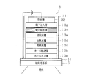
- FIG. 1 is a cross-sectional view schematically showing an organic EL element formed using the film forming system according to Embodiment 1.
- FIG. 1 is a cross-sectional view schematically showing an organic EL element formed using the film forming system according to Embodiment 1.
- FIG. 6 is a side sectional view showing a film forming head according to Embodiment 3.
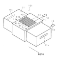
- FIG. It is a perspective view which shows typically the structure of the film-forming apparatus which concerns on Embodiment 4 of this invention.
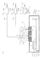
- FIG. 6 is a side sectional view schematically showing a configuration of a film forming apparatus according to a fourth embodiment.
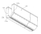
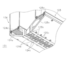
- FIG. 10 is a perspective view schematically showing an example of a configuration of a first film formation material supply unit and a second film formation material supply unit according to Embodiment 4.
- FIG. 25 is a partially enlarged view of FIG. 24.
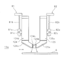
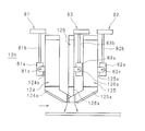
- FIG. 10 is a front view schematically showing an example of a configuration of a first film formation material supply unit and a second film formation material supply unit according to Embodiment 4.
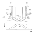
- An example of the arrangement of the first film formation material supply unit and the second film formation material supply unit according to Embodiment 4 and the amount of vapor in the transport direction of the first film formation material and the second film formation material are conceptually shown. It is explanatory drawing shown. It is a perspective view which shows typically an example of the structure of the film-forming apparatus which concerns on Embodiment 5 of this invention.
- FIG. 10 is a side sectional view schematically showing an example of a configuration of a film forming apparatus according to a fifth embodiment.
- FIG. 10 is a perspective view schematically showing an example of a configuration of a first film formation material supply unit and a second film formation material supply unit according to Embodiment 5.
- FIG. 31 is a partially enlarged view of FIG. 30.
- FIG. 10 is a front view schematically showing an example of a configuration of a first film formation material supply unit and a second film formation material supply unit according to Embodiment 5. It is a front view which shows typically the structure of the 1st film-forming material supply part which concerns on Embodiment 6 of this invention, the 2nd film-forming material supply part, and the 3rd film-forming material supply part.
- FIG. 10 is a partial bottom view schematically showing configurations of a first film formation material supply unit, a second film formation material supply unit, and a third film formation material supply unit according to Embodiment 6.
- FIG. 1 is an explanatory diagram conceptually illustrating the configuration of a film forming system including a film forming apparatus according to Embodiment 1 of the present invention.
- the film forming system according to the present embodiment includes a loader 90, a transfer chamber 91, a film forming apparatus 1, a transfer chamber 92, an etching apparatus 93, which are arranged in series along the transfer direction of the substrate G to be processed (see FIG. 3).
- a transfer chamber 94, a sputtering apparatus 95, a transfer chamber 96, a CVD apparatus 97, a transfer chamber 98, and an unloader 99 are provided.
- a gate valve (not shown) is provided between each device.
- the loader 90 carries the substrate G to be processed, for example, the substrate G on which the ITO layer 31 has been previously formed, into the film forming system.
- the transfer chambers 91, 92, 94, 96, and 98 deliver the substrate G to be processed between the processing apparatuses.
- the film forming apparatus 1 is formed by applying a hole injection layer, a hole transport layer, a blue light emitting layer, a red light emitting layer, a green light emitting layer, an electron transport layer, and an electron injection layer (cathode layer) on the substrate G to be processed by vacuum deposition. Form. Details will be described later.
- the etching apparatus 93 is an apparatus for adjusting the shape of the organic layer to a predetermined shape.
- the sputtering apparatus 95 is an apparatus that forms a cathode layer on an electron transport layer by sputtering, for example, silver (Ag), magnesium silver (Mg / Ag) alloy, or the like using a pattern mask.
- the CVD apparatus 97 forms a sealing layer made of a nitride film such as silicon nitride (SiN) by a chemical vapor deposition (CVD) method and seals each layer formed on the substrate G to be processed. It is a device.
- the unloader 99 is an apparatus for carrying the substrate to be processed G out of the film forming system.
- FIG. 2 is a perspective view schematically showing the configuration of the film forming apparatus 1
- FIG. 3 is a side sectional view schematically showing the configuration of the film forming apparatus 1.
- the film forming apparatus 1 includes a processing chamber 11 for accommodating a substrate to be processed G and for performing a film forming process on the substrate to be processed G by vapor deposition.
- the processing chamber 11 has a hollow, substantially rectangular parallelepiped shape in which the transport direction is the longitudinal direction and the central portion is wide, and is made of aluminum, stainless steel, or the like. A surface of one end in the longitudinal direction of the processing chamber 11 (a surface on the back side in FIG.
- the carry-in port 11a and the carry-out port 11b have a slit shape having a longitudinal direction orthogonal to the carry-in direction, and the longitudinal directions of the carry-in port 11a and the carry-out port 11b are substantially the same.
- the longitudinal direction of the carry-in port 11a and the carry-out port 11b is referred to as a horizontal direction
- the direction perpendicular to the horizontal direction and the conveyance direction is referred to as a vertical direction.
- an exhaust hole 11 c is formed at an appropriate position of the processing chamber 11, and a vacuum pump 15 disposed outside the processing chamber 11 is connected to the exhaust hole 11 c through an exhaust pipe 14.
- a vacuum pump 15 disposed outside the processing chamber 11 is connected to the exhaust hole 11 c through an exhaust pipe 14.
- the vacuum pump 15 is driven, the inside of the processing chamber 11 is depressurized to a predetermined pressure, for example, 0.01 Pa.
- the transfer device 12 includes a guide rail 12a provided at the bottom of the processing chamber 11 along the longitudinal direction, and a moving member 12b that is guided by the guide rail 12a and is movable in the transfer direction, that is, the longitudinal direction. And a support 12c that is provided on the upper surface of the moving member 12b and supports the substrate G to be processed so as to be substantially parallel to the bottom.
- An electrostatic chuck that holds the substrate to be processed G, a substrate heater to be processed to keep the temperature of the substrate to be processed G constant, a refrigerant pipe, and the like are provided inside the support base 12c.
- the support base 12c is configured to move by a linear motor.
- a plurality of vapor deposition heads 13 for forming a film on the substrate G to be processed by a vacuum vapor deposition method are provided in the upper portion of the processing chamber 11 and in the substantially central portion in the transport direction.
- the vapor deposition head 13 includes a first head 13a for vapor-depositing a hole injection layer, a second head 13b for vapor-depositing a hole transport layer, a third head 13c for vapor-depositing a blue light-emitting layer, a fourth head 13d for vapor-depositing a red light-emitting layer, and green.
- the fifth head 13e for depositing the light emitting layer, the film forming head 2 for depositing the electron transport layer according to the present invention, and the sixth head 13f for depositing the electron injection layer are arranged in order along the transport direction. Yes.
- the film forming head 2 is a head for co-evaporating an organic film forming material such as Alq 3 and an inorganic film forming material.
- the film forming head 2 includes an organic film forming material supply unit 4 and an inorganic film forming material supply unit 5 described later.
- An organic film-forming material is supplied to the film-forming head 2 through a pipe 16 from a vapor generation unit 17 disposed outside the processing chamber 11.
- Examples of the inorganic film forming material include materials having a work function lower than that of Alq 3 , which is 3.0 (eV), such as Li (work function: 2.5 (eV)), Na (2.28 ( eV)), K (2.24 (eV)), Ca (2.71 (eV)), Cs (1.81 (eV)), Ba (2.11 (eV)), and the like. Can be mentioned.
- the steam generation unit 17 includes a container 17a and a heating mechanism 17b disposed inside the container 17a.
- the heating mechanism 17b has a container-like portion that can store the vapor of the organic film forming material, and is configured to heat the organic film forming material with electric power supplied from the power source 17c. For example, it is configured to heat with an electric resistor.
- the organic film forming material stored in the heating mechanism 17b is heated to generate vapor of the organic film forming material.
- the container 17a is connected to a transport gas supply pipe 17d that supplies a transport gas made of an inert gas such as Ar to the substrate G to be processed, and is supplied from the transport gas supply pipe to the container 17a.
- the vapor of the organic film forming material is supplied from the vapor generating unit 17 to the film forming head 2 via the pipe 16.
- the first to fifth heads 13a, 13b, 13c, 13d, and 13e are configured such that a vapor of a predetermined organic film forming material is supplied from a vapor generation unit (not shown).
- a vapor of a predetermined inorganic film forming material is also supplied to the sixth head 13f from a vapor generation unit (not shown).
- the inorganic film forming material may not be received from the vapor generation unit, and the vapor of the inorganic film forming material may be generated in the sixth head 13f.
- sputtering or the like may be performed in a processing chamber outside the processing chamber 11. Alternatively, the film may be formed.
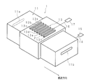
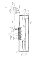
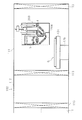
- FIG. 4 is a side sectional view showing the film forming head 2.
- the film formation head 2 has an organic film formation material supply unit (organic vapor supply unit) 4 that ejects vapor of the organic film formation material toward the substrate G to be processed, and directs vapor of the inorganic film formation material toward the substrate G to be processed. And an inorganic film-forming material supply unit 5 (inorganic vapor supply unit) that jets out.
- the organic film forming material supply unit 4 and the inorganic film forming material supply unit 5 are arranged so that the portions to be ejected of the organic film forming material and the inorganic film forming material overlap on the substrate G to be processed.
- the organic film forming material supply unit 4 has an organic film forming material ejection hole 41a through which the vapor of the organic film forming material is jetted, and an organic film forming material casing 41 into which the vapor of the organic film forming material flows from the outside, Organic film forming material heaters 42a, 42b, 42c, 42d that are fed by a power supply member (not shown) to heat the organic film forming material casing 41, and a heat medium flow path 43a that allows a heat medium such as air to flow therethrough. , 43b.
- the organic film forming material heaters 42a, 42b, 42c, 42d and the heat medium passages 43a, 43b are embedded in the organic film forming material casing 41 by heater fixing members 41b, 41c, 41d, 41e. .
- the organic film forming material casing 41 has a substantially rectangular frame member 411 whose longitudinal direction is substantially perpendicular to the paper surface, and a hollow plate is formed from the substantially central portion of the lower surface of the frame member 411 toward the inorganic film forming material supply unit 5 side.
- the member 412 protrudes.
- the organic film forming material ejection hole 41 a through which the organic film forming material flowing through the inside of the frame member 411 and the hollow plate member 412 is ejected is formed at the tip of the hollow plate member 412.
- a plurality of recesses for embedding the organic film forming material heaters 42a and 42b and the heat medium passages 43a and 43b are formed on the outer surface of the hollow plate member 412.
- the concave portion has, for example, a substantially arc shape when viewed from the side.
- the organic film forming material heaters 42a and 42b and the heat medium passages 43a and 43b are cylindrical in shape, and a good heat conductive film such as a carbon graphite film is wound around the outer peripheral surface thereof. It is inserted into a plurality of recesses.
- the organic film forming material heaters 42a and 42b and the heat medium passages 43a and 43b fitted in the recesses are fixed by heater fixing members 41d and 41e.
- the heater fixing members 41d and 41e are plate-like members corresponding to the outer surface of the hollow plate member 412, and have recesses that fit into the organic film forming material heaters 42a and 42b and the heat medium passages 43a and 43b. ing.
- the shape of the recess is substantially semicircular when viewed from the side, as with the recess formed in the hollow plate member 412.
- the heater fixing members 41d and 41e are fixed to the organic film forming material casing 41.
- organic film forming material heaters 42c and 42d are fitted on the upper surface of the frame member 411, and are fixed to the frame member 411 by heater fixing members 41b and 41c.
- An organic film forming material supply pipe 40 through which the vapor of the organic film forming material generated by the vapor generating unit 17 flows into the organic film forming material casing 41 is connected to a substantially central portion of the upper portion of the frame member 411. .
- the organic film forming material supply pipe 40 is made of, for example, stainless steel, and either the outer or inner surface of the organic film forming material supply pipe 40 or the outer and inner surfaces are electrically conductive such as copper plating in order to improve heat conduction. Coated with a functional film.
- the film forming head 2 includes supply pipe heaters 61 and 62 for heating the organic film forming material supply pipe 40. Since the organic film forming material supply unit 4 is configured as described above, the material of the organic film forming material passed through the pipe 16 and the organic film forming material supply pipe 40 from the vapor generation unit 17 is kept warm. In the state, it is ejected from the ejection hole 41a.
- the inorganic film forming material supply section 5 includes a hollow inorganic film forming material casing 51.
- the inorganic film-forming material casing has a substantially hollow cylindrical shape whose longitudinal direction is substantially perpendicular to the paper surface, and the lower part projects toward the organic film-forming material supply unit 4 side.
- a plurality of inorganic film-forming material ejection holes 51a are formed uniformly along the both ends in the longitudinal direction on the lower surface of the protruding portion.
- a container 57 in which an inorganic film forming material that is an electron injection layer material, for example, an alkali metal, is charged is supported by the heating device 54 inside the inorganic film forming material casing 51.
- the container 57 is in the shape of a square dish and has an opening 57a on the upper surface for sending the vapor of the inorganic film forming material into the inorganic film forming material casing 51.
- FIG. 5 is a side view showing the heating device 54
- FIG. 6 is a front view showing the heating device 54
- FIG. 7 is a sectional view taken along the line VII-VII in FIG.
- the heating device 54 has a first half 54a constituting the lower side of the heating device 54 and a second half 54b constituting the upper side of the heating device 54. On the upper surface of the second half 54b, A groove portion into which the container is fitted is formed.
- the first and second halves 54a and 54b are made of metal.
- a plurality of recesses for embedding the first heaters 55a and 55b and the first heat medium flow path 56 are formed on the upper surface of the first half 54a.
- the recess has a substantially arc shape.
- the first heaters 55a and 55b and the first heat medium flow path 56 which are supplied with power by a power supply member (not shown) and heat the container 57, each have a cylindrical shape, and the outer peripheral surface has good heat conductivity.
- a film such as a carbon graphite film is wound and fitted into the plurality of recesses.
- the first heaters 55a and 55b and the first heat medium flow path 56 fitted in the recess are fixed so as to be sandwiched by the second half 54b.
- the second half 54 b is a plate-like member corresponding to the first half 54 a and has a recess that fits into the first heaters 55 a and 55 b and the first heat medium flow path 56.
- the shape of the recess is substantially semicircular when viewed from the side, as with the recess formed in the hollow plate member 412.
- the first and second halves 54a and 54b are welded all around, but the first and second halves 54a and 54b may be joined by screws. Both ends of the first heat medium flow channel 56 are connected to an air cooling device (not shown), and the air cooling device allows air to flow through the first heat medium flow channels 56b and 56c.
- second heaters 52a, 52b, 52c, 52d, 52e, and 52f, and second heat medium passages 53a and 53b which are fed by a power feeding member (not shown), are provided.
- 53c are formed, and the second heaters 52a, 52b, 52c, 52d, 52e, 52f and the second heat medium flow channels 53a, 53b, 53c are fitted in the recesses.
- the second heaters 52a, 52b, 52c, 52d, 52e, 52f and the second heat medium passages 53a, 53b, 53c are connected to the inorganic film-forming material casing 51 by the heater fixing members 51b, 51c, 51d.
- both ends of the second heat medium passages 53a, 53b, 53c are connected to an air cooling device (not shown), and the air cooling device allows air to flow through the second heat medium passages 53a, 53b, 53c. ing.
- the said air cooling apparatus is comprised so that the direction which lets air flow through may be switched periodically. By periodically switching the direction in which the air flows, it is possible to prevent a temperature difference from occurring between the one end portion and the other end portion of the inorganic film forming material casing 51 in the longitudinal direction of the container 57. It becomes possible to improve thermal uniformity.
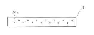
- FIG. 8 is a schematic view showing an arrangement example of the inorganic film forming material ejection holes 51a.
- the inorganic film forming material ejection holes 51a are arranged in a staggered manner, for example, as shown in FIG.
- the arrangement of the inorganic film forming material ejection holes 51a is an example.
- the vapor of the inorganic film forming material generated by heating the first heaters 55a and 55b is the second heaters 52a, 52b, 52c, 52d, 52e, and 52f. In a state where the temperature is maintained by the above, it is ejected from the ejection hole 51a.
- the film forming head 2 includes an organic film forming material supply unit 4 and an inorganic film forming material supply unit 5, a heat insulating cover 71 for an organic material supply unit that blocks heat radiated to the substrate G, and an inorganic film forming material. And a heat insulating cover 72 for the supply unit 5 (see FIG. 4). Between the heat shield cover 71 and the heat shield cover 72, a heat shield plate 73 having a flow passage 73a through which cooling water or cooling gas flows is provided.
- the heat insulating cover 71 and the heat insulating cover 72 are not limited to the case where the heat insulating cover 71 and the heat insulating plate 73 are provided.
- the heat insulating cover 73 and the heat insulating plate 73 are included. Also good.
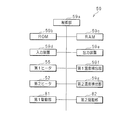
- FIG. 9 is a block diagram showing a configuration example of the control device 59 that controls the operation of the film forming head 2.
- the control device 59 has a control unit 59a such as a CPU (Central Processing Unit).
- a control unit 59a such as a CPU (Central Processing Unit).
- At least the first heaters 55a and 55b (hereinafter referred to as the first heater 55) and the second heaters 52a, 52b, 52c, 52d, 52e and 52f (denoted by the film forming head 2) are connected to the control unit 59a via a bus.
- a ROM 59b storing a computer program for controlling the operation of the second heater 52
- a RAM 59c for temporary storage
- an input device 59d such as a keyboard and a mouse
- an output device 59e such as a display device
- a first heater 55, a second heater 52, a first temperature detection unit 59f, a second temperature detection unit 59g, a first drive unit 81, which will be described later, and a second drive unit 82 are connected.
- the first temperature detection unit 59f detects the ambient temperature T1 of the first heater 55, for example, the temperature of the first half 54a (container 57) of the heating device 54, and gives the detected temperature to the control unit 59a.
- the second temperature detection unit 59g detects the ambient temperature T2 of the second heater 52, for example, the temperature of the inorganic film forming material casing 51, and supplies the detected temperature to the control unit 59a.
- the first and second heaters 55 and 52 and the first and second drive units 81 and 82 are connected to the bus through a power supply circuit connected to the I / O port. The / O port and the power supply circuit are not shown.
- the control unit 59a Based on the detection results of the first and second temperature detection units 59f and 59g, the control unit 59a makes the first and second temperature detection units 59f and 59g so that the ambient temperature T1 of the inorganic film forming material supply unit 5 reaches a specific target temperature. 2 Power supply to the heaters 55 and 52 is controlled.
- the target temperature is a temperature at which a vapor amount of a required inorganic film forming material (vapor deposition material) can be obtained during film formation.
- FIG. 10 is a timing chart showing the power supply to the first heater 55 and the second heater 52 and the temperature change of the container 57.
- the horizontal axis represents time
- the vertical axis represents temperature.
- the time-dependent change of the above-mentioned ambient temperature T1 and ambient temperature T2 is shown by a graph.
- the controller 59a starts supplying power to the first heater 55 and the second heater 52 by giving a control signal to the power supply circuit.
- the control unit 59a detects the ambient temperature T1 of the first heater 55 (the temperature of the container 57) T1 and the ambient temperature T2 of the second heater 52 using the first and second temperature detection units 59f and 59g, and at least described later.
- the temperature is increased while the outputs of the first heater 55 and the second heater 52 are controlled so that the ambient temperature T2 becomes higher than the ambient temperature T1 at the first temperature.
- the control unit 59a decreases the amount of power supplied to the first heater 55.
- the first temperature is a temperature at which vapor of the inorganic film forming material starts to be generated, and is a temperature lower than the target temperature.
- the control unit 59a determines whether the ambient temperature T2 of the second heater 52 has reached the second temperature using the second temperature detection unit 59g.
- the second temperature is higher than the target temperature, and when the ambient temperature T2 of the second heater 52 reaches the second temperature, the power supply to the first heater 55 and the second heater 52 is controlled by PID control.
- the temperature of the container 57 and the inorganic film forming material can be converged to the target temperature by the heat radiated from the periphery of the two heaters 52 and the heating from the first heater 55.
- the second temperature may be a predetermined temperature determined by experiments or the like, or may be a temperature calculated based on the input target temperature. For example, when the target temperature is 500 degrees, 520 degrees is set as the second temperature.
- the control unit 59a determines that the ambient temperature T2 of the second heater 52 has reached the second temperature
- the control unit 59a performs PID control on the first heater 55 and the second heater 52 to perform a film forming process.
- the control unit 59a monitors the temperatures detected by the first and second temperature detection units 59f and 59g, and gives a control signal to the power supply circuit so that the ambient temperature T1 matches the target temperature.
- the power supply to the first heater 55 and the second heater 52 is controlled. More specifically, when the ambient temperature T2 becomes equal to or higher than the second temperature, the control unit 59a temporarily stops heating by the second heater 52 or decreases the output, and the ambient temperature T2 becomes lower than the second temperature.
- the heating by the second heater 52 is resumed or increased.
- the heating by the first heater 55 is stopped or the output is reduced.
- the heating by the first heater 55 is performed. Resume or increase.
- the ambient temperature T1 is maintained at the target temperature. Even when heating of the inorganic film forming material is stopped, the temperature of the container 57 and the inorganic film forming material is decreased while maintaining the condition that the ambient temperature T1 is equal to or lower than the ambient temperature T2. This prevents vapor of the inorganic film forming material from adhering to the inner wall of the inorganic film forming material casing 51.
- the inorganic film-forming material can be uniformly heated at the target temperature in the container 57 that has a predetermined length and tends to be non-uniform in the longitudinal direction only by the heating control by the first heater 55. Become. That is, the temperature uniformity in the longitudinal direction of the container 57 can be improved.
- FIG. 11 is a timing chart showing power supply to the first heater 55 and the second heater 52 and the temperature change of the container 57 in another example.
- the controller 59a raises the temperature in a state where the ambient temperature T1 and the ambient temperature T2 substantially match (however, control is performed so that the ambient temperature T2 is always equal to or higher than the ambient temperature T1).
- the ambient temperature T1 reaches the first temperature
- the amount of power supplied to the first heater 55 is decreased.
- the second heater 52 is controlled by PID so that the ambient temperature T1 converges to the target temperature.
- the container 57 can be uniformly heated to the target temperature in the longitudinal direction, and the inorganic film forming material can be uniformly heated at the target temperature.
- the first temperature and the second temperature of this process may be set to values different from the first temperature and the second temperature of the process of FIG.
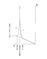
- FIG. 12 shows the arrangement of the organic film forming material supply unit 4 and the inorganic film forming material supply unit 5 and the transport direction of the organic film forming material and the inorganic film forming material (the end on the carry-in port 11a side below the film forming head 2). It is explanatory drawing which showed notionally the vapor quantity in the distance from a part).
- A is a graph showing the vapor amount of the inorganic film forming material
- B is a graph showing the vapor amount of the organic film forming material.
- the organic film forming material supply unit 4 and the inorganic film forming material supply unit 5 are connected to the organic film forming material supply unit 4 and the inorganic film forming material supply unit 5 in the vertical direction (vertical direction) and the horizontal direction (conveyance of the substrate G to be processed).
- the first drive unit 81 and the second drive unit 82 for movement in the direction) are attached.
- the first drive unit 81 and the second drive unit 82 are provided in the upper part of the processing chamber 11.
- the first drive unit 81 and the second drive unit 82 include support portions 81 a and 82 a that support the organic film formation material supply unit 4 and the inorganic film formation material supply unit 5, and screw shaft portions 81 b and 82 b.
- the support portions 81a and 82a are each provided with two shaft portions 81c and 82c protruding in a direction perpendicular to the paper surface of FIG. 12, and the heat-shielding cover 71 and the light-shielding cover 71 of the organic film-forming material supply section 4 and the inorganic film-forming material supply section 5
- the thermal cover 72 includes two protruding portions 4c and 5c that are fitted to the shaft portions 81c and 82c.
- the first driving unit 81 and the second driving unit 82 rotate the screw shafts 81b and 82b by a ball screw mechanism, so that the organic film forming material supply unit 4 and the inorganic film forming material supply unit 5 are interposed via the support units 81a and 82a.
- the support portions 81a and 82a can be moved in the horizontal direction by a microstage, and the organic film forming material supply unit 4 and the inorganic film forming material supply unit 5 are configured to move in the horizontal direction.
- the protruding portions 4c and 5c rotate around the shaft portions 81c and 82c, so that the organic film forming material supply unit 4 and the inorganic film forming material supply unit 5 rotate in the ⁇ direction.
- the first driving unit 81 and the second driving unit 82 are controlled by the control unit 59a to move the organic film forming material supply unit 4 and the inorganic film forming material supply unit 5 to appropriate positions.
- the organic film forming material supply unit 4 and the inorganic film forming material supply unit 5 are moved in the vertical and horizontal directions, and the organic film forming material supply unit 4 and the inorganic film forming material supply unit 5 are rotated in the ⁇ direction.
- the configuration is not limited to the above case.
- the organic film forming material supply unit 4 and the inorganic film forming material supply unit 5 may be moved in the vertical direction by a micrometer, or may be moved in the horizontal direction by a ball screw mechanism or a linear motor.
- the inorganic film forming material is mostly contained immediately above the light emitting layer in accordance with the transport of the substrate G to be processed.
- a film is formed, and the film is formed so that the mixing amount of the organic film forming material gradually increases.
- the mixing ratio (volume ratio) between the inorganic film-forming material and the organic film-forming material is about 50:50 at the substantially central portion in the film thickness direction, and then the film is formed with a high ratio of the organic film-forming material. Is formed in a state where most of the organic film forming material is contained, and the film forming process is completed.
- FIG. 13 is a cross-sectional view schematically showing the organic EL element 3 formed using the film forming system according to the first embodiment.
- the substrate G to be processed, on which the ITO layer 31 is formed in advance is carried into the film forming system from the loader 90, and is further carried into the film forming apparatus 1 in the back by the transfer chamber 91.
- the transfer chamber 91 and the loader 90 are connected via a gate valve (not shown).
- the substrate G to be processed carried into the processing chamber 11 of the film forming apparatus 1 is electrostatically adsorbed on the support 12c shown in FIG. 3 with the surface, that is, the ITO layer 31 facing upward, and is held at a constant temperature.
- the inside of the processing chamber 11 is previously depressurized to a predetermined pressure, for example, 0.01 Pa or less by driving the vacuum pump 15.
- the support base 12c moves in the transport direction along the guide rail 12a, and the substrate G to be processed passes below the vapor deposition head 13. In the process of passing under the vapor deposition head 13, as shown in FIG.
- the target substrate G includes a hole injection layer 33a, a hole transport layer 33b, a blue light emitting layer 33c, a red light emitting layer 33d, and a green light emitting layer 33e.
- a hole injection layer 33a is sequentially formed.
- the film formation head 2 the vapor deposition of the organic film formation material and the inorganic film formation material is co-deposited with the organic film formation material and the inorganic film formation material in a state where the mixing ratio is controlled in the film formation direction.
- a transport layer 33f is formed.
- the electron injection layer 33g is formed.
- the substrate G to be processed after the organic layer and inorganic layer forming processes are carried into the etching apparatus 93 by the transfer chamber 92.
- the etching apparatus 93 the shape and the like of various films are adjusted.
- it is carried into the sputtering apparatus 95 by the transfer chamber 94.
- the sputtering apparatus 95 the cathode layer 32 is formed.
- the substrate G to be processed is carried into the CVD apparatus 97 by the transfer chamber 96.
- each layer formed on the substrate G to be processed is sealed with a sealing layer 34 such as a silicon nitride (SiN) film.
- a sealing layer 34 such as a silicon nitride (SiN) film.
- the target substrate G subjected to the sealing process is carried out of the film forming system from the unloader 99 via the transfer chamber 98.
- an organic film-forming material Alq 3 having a vapor pressure of 10 Pa at 450 ° C. is supplied to the organic film-forming material supply unit 4 and ejected, and an inorganic film-forming material Ba having a vapor pressure of 10 Pa at 700 ° C. is ejected.
- Co-deposition can be performed after mixing so as to have a concentration distribution.
- the electron injection layer is formed in the film forming direction (film thickness direction) of the electron transport layer 33g.
- the mixing ratio of the inorganic film forming material increases from 33 g toward the green light emitting layer 33 e.
- FIG. 13 schematically shows the concentration distribution in this case.
- the arrangement of the organic film forming material supply unit 4 and the inorganic film forming material supply unit 5 is not limited to the arrangement shown in FIG.
- the positions of the organic film forming material supply unit 4 and the inorganic film forming material supply unit 5 can be adjusted. Specifically, based on the electron transport characteristics of the inorganic film-forming material and the organic film-forming material, the energy of the green light emitting layer 33e side and the electron injection layer 33g side interface is secured while sufficiently preventing the hole film from penetrating.
- the positions of the organic film forming material supply unit 4 and the inorganic film forming material supply unit 5 are adjusted so as to adjust the height of the barrier, and the concentration distribution of the inorganic film forming material in the film forming direction is controlled.
- FIG. 14 is an explanatory view showing another arrangement example and concentration distribution of the organic film forming material supply unit 4 and the inorganic film forming material supply unit 5, and FIG. 15 schematically shows the organic EL element formed in the arrangement example. It is sectional drawing shown.
- A is a graph showing the vapor amount of the inorganic film forming material
- B is a graph showing the vapor amount of the organic film forming material.
- the organic film forming material supply unit 4 protrudes below the inorganic film forming material supply unit 5.
- the concentration of the inorganic film forming material is increased on the green light emitting layer 33e side and the electron injection layer 33g side.
- FIG. 16 is an explanatory view showing another arrangement example and concentration distribution of the organic film forming material supply unit 4 and the inorganic film forming material supply unit 5, and FIG. 17 schematically shows the organic EL element formed in the arrangement example.
- A is a graph showing the vapor amount of the inorganic film forming material
- B is a graph showing the vapor amount of the organic film forming material.
- the organic film forming material supply unit 4 is disposed on the upstream side in the transport direction of the substrate G to be processed, and the inorganic film forming material supply unit 5 is disposed on the downstream side in the transport direction.
- the concentration of the inorganic film-forming material increases as it goes from the green light emitting layer 33e side to the electron injection layer 33g side.
- the height of the energy barrier at the interface between the electron transport layer 33f and the green light-emitting layer 33e and the interface with the electron injection layer 33g is adjusted, so that the electron
- the holes are reliably prevented from penetrating from the green light emitting layer 33e side to the cathode layer 32, the deterioration of the cathode interface is suppressed, and the light emission efficiency is improved.
- the concentration distribution in the film thickness direction is appropriately set according to the organic film forming material and the inorganic film forming material, and the interface between the green light emitting layer 33e side and the electron injection layer 33g side of the electron transport layer 33f.
- the electron injection rate can be controlled by adjusting the state.
- the height of the energy barrier at the light emitting layer side interface and the cathode side interface of the film is increased. It is possible to control the electron injection efficiency to improve the light emission efficiency and to solve the problem of manufacturing an organic light emitting device having good light emission intensity.
- the first driving unit 81 and the second driving unit 82 are configured to be able to move the organic film forming material supply unit 4 and the inorganic film forming material supply unit 5 in the horizontal direction and the vertical direction, although the case where it is configured to be rotatable in the ⁇ direction has been described, the present invention is not limited to this.
- the first driving unit 81 and the second driving unit 82 may move the organic film forming material supply unit 4 and the inorganic film forming material supply unit 5 only in the horizontal direction. However, it is preferable to be able to move in the vertical direction and to be rotatable in the ⁇ direction because the density distribution can be finely controlled.
- the organic film forming material supply unit 4 and the inorganic film forming material supply unit 5 are not limited to being moved automatically, and may be moved manually. Furthermore, although the case where the first drive unit 81 and the second drive unit 82 are provided in the upper portion of the processing chamber 11 is described, the present invention is not limited to this. For example, the film is formed by jetting steam from the lower side of the processing chamber 11 In some cases, the first drive unit 81 and the second drive unit 82 may be provided below the processing chamber 11. In the present embodiment, the case where both the organic film forming material supply unit 4 and the inorganic film forming material supply unit 5 are configured to be movable is described, but the present invention is not limited to this. Only one of them may be configured to be movable.
- the organic film forming material supply unit 4 includes the organic film forming material supply pipe 40 whose front end protrudes from the upper surface of the processing chamber 11, the inorganic film forming material supply unit 5 provided in the processing chamber 11 is provided. It is preferable to configure it to be movable.
- FIG. 18 is a perspective view showing a film forming apparatus 101 according to the second embodiment. In the figure, the same parts as those in FIG. As described above, the film forming apparatus 101 does not have the sixth head 13f as the vapor deposition head 13, but the first head 13a for vapor deposition of the hole injection layer, the second head 13b for vapor deposition of the hole transport layer, and the blue light emitting layer.
- the third head 13c to be deposited, the fourth head 13d to deposit the red light emitting layer, the fifth head 13e to deposit the green light emitting layer, and the film forming head 202 are sequentially arranged along the transport direction.
- the film forming head 202 has the same configuration as the film forming head 2 according to the first embodiment. That is, it has the same configuration as that shown in FIG.
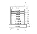
- FIG. 19 is a cross-sectional view schematically showing an organic EL element 303 formed using the film forming apparatus 101 according to the second embodiment.
- a hole injection layer 33a, a hole transport layer 33b, a blue light emitting layer 33c, a red light emitting layer 33d, and a green light emitting layer 33e are sequentially formed on the target substrate G.
- the organic film formation material and the inorganic film formation material are applied to the substrate G to be processed in a state where the mixing ratio of the vapor of the organic film formation material and the inorganic film formation material is controlled in the film formation direction. Co-evaporation is performed. That is, an electron transport / injection layer 33h in which an organic film forming material and an inorganic film forming material are mixed is formed on the substrate G to be processed.
- the organic film forming material supply unit 4 and the inorganic film forming material supply unit 5 are arranged as described above, the concentration of the inorganic film forming material increases from the cathode layer 32 side toward the green light emitting layer side 33e side. The film is formed so as to increase.
- the cathode layer 32 is formed from the green light emitting layer side 33e side as in the first embodiment.
- a predetermined electron injection efficiency can be obtained by adjusting the energy barrier to a desired value, and the obtained organic EL device has a good emission intensity.
- Embodiment 3 The film forming apparatus 102 of the film forming system according to the third embodiment of the present invention performs film formation up to the green light emitting layer 33e in the processing chamber 11, and the processing chamber 111 independent of the processing chamber 11 from the electron transport / injection layer 33i.
- the configuration is the same as that of the film forming system according to Embodiments 1 and 2 except that the configuration is performed as described above. Since the film formation up to the electron transport layer 33f is performed in the same manner as in the first and second embodiments, detailed description thereof is omitted.
- FIG. 20 is an explanatory diagram conceptually illustrating a part of the film forming apparatus 102 according to the third embodiment
- FIG. 21 is a side sectional view showing the film forming head 203 according to the third embodiment.
- the film forming head 203 includes the organic film forming material supply unit 4 and the inorganic film forming material supply unit 5 according to the first embodiment.
- the metal film-forming head 203 having a box shape mixes the organic film-forming material ejected from the organic film-forming material supply unit 4 and the inorganic film-forming material ejected from the inorganic film-forming material supply unit 5.
- the mixing chamber 204 is provided on the bottom surface.
- a jet outlet 203a for jetting the mixed film forming material is provided on the bottom surface of the mixing chamber 204.
- the organic film forming material supply pipe 40 of the organic film forming material supply unit 4 penetrates the upper surface of the film forming head 203, and a flow rate adjusting unit 80 is provided at a portion protruding from the upper surface.
- the organic film forming material is supplied to the film forming head 203 in a state where the flow rate of the organic film forming material supplied from the vapor generating unit 17 is controlled by the flow rate adjusting unit 80.
- the processing chamber 11 and the processing chamber 111 are connected via a gate valve 113, a transfer module 112, and a gate valve 113.
- the to-be-processed substrate G formed up to the green light emitting layer 33e is configured to be transferred from the processing chamber 11 to the processing chamber 111 by a robot arm or the like via the transfer module 112.
- the support stand 12c which supports the to-be-processed substrate G is comprised so that the inside of the process chamber 111 may be conveyed in the longitudinal direction of the film-forming apparatus 102 by the moving member 12b.
- the film formation head 203 may be configured to be movable in the longitudinal direction above the substrate G to be processed.
- the mixing amount (supply amount) of the organic film forming material with respect to the inorganic film forming material is controlled step by step, and the green light emitting layer 33e is provided below the jet port 203a of the film forming head 203 in each step.
- the film-formed substrate G is conveyed in the longitudinal direction, or the film-forming head 203 is moved in the longitudinal direction, and the mixed film-forming material is ejected onto the substrate G to be processed in the film thickness direction. Then, an electron transport / injection layer 33i having a controlled concentration distribution is formed.
- the organic film forming material supply unit 4 and the inorganic film forming material supply unit 5 are juxtaposed in the transport direction of the processing substrate G, and the electron transport layer 33f or the electrons are transported while transporting the target substrate G. Since the transport / injection layer 33h is formed, as shown in FIG. 12, the thickness of the portion having the composition on the center side is larger than the thickness of the portion having the composition on the end portion side in the film thickness direction of the film formation. .
- the mixing amount of the organic film forming material can be increased by a constant amount every predetermined time, and the thickness of each composition in the film forming direction can be made substantially uniform.
- the green light emitting layer 33e side to the cathode layer 32 side is provided as in the first embodiment. While preventing hole penetration and preventing deterioration of the cathode interface, energy barriers at the interface between the green light emitting layer 33e and the electron transport / injection layer 33i and at the interface between the cathode layer 32 and the electron transport / injection layer 33i The electron injection efficiency can be adjusted to adjust the emission intensity.
- the present invention is not limited to this, and the film formed up to the green light emitting layer side 33e is not limited thereto.
- An electron transport layer may be formed on the processing substrate G by the film forming apparatus 102, and an electron injection layer may be further formed.
- the present invention is not limited to the case where the supply amount of the organic film forming material is controlled and mixed with the inorganic film forming material, and the supply amount of the inorganic film forming material may be controlled. The supply amount of both inorganic film forming materials may be controlled.
- the present invention is not limited to this. is not.
- FIG. 22 is a perspective view schematically showing the configuration of the film forming apparatus 121 according to Embodiment 4, and FIG. 23 is a side sectional view schematically showing the configuration of the film forming apparatus 121.
- FIG. 23 is a side sectional view schematically showing the configuration of the film forming apparatus 121.
- a plurality of vapor deposition heads 13 that deposit a film on the substrate G to be processed by a vacuum vapor deposition method are provided in the upper portion of the processing chamber 11 of the film forming apparatus 121 and in the substantially central portion in the transport direction.
- the vapor deposition head 13 includes a first head 13a for vapor-depositing a hole injection layer, a second head 13b for vapor-depositing a hole transport layer, a third head 13g for vapor-depositing a blue light-emitting layer, a fourth head 13d for vapor-depositing a red light-emitting layer, and green.
- the fifth head 13e for depositing the light emitting layer, the sixth head 13f for depositing the electron transport layer, and the film forming head 122 having the same configuration as that of the invention according to the first embodiment are arranged in order along the transport direction.
- the film formation head 122 may be capable of changing the positions of the organic film formation material supply unit 4 and the inorganic film formation material supply unit 5 in the same manner as the film formation head 2 of the film formation apparatus 1 of the first embodiment. The position may be fixed.
- the third head 13g is a device for co-evaporating the first film forming material and the second film forming material.
- the third head 13g includes a second film-forming material supply unit 124 and a first film-forming material supply unit 125 in order from the upstream side in the transport direction of the substrate G to be processed.
- the second film formation material supply unit 124 and the first film formation material supply unit 125 are supplied with gaseous second film formation material and first film formation material from the steam generation units 145 and 146.
- the steam generation units 145 and 146 include containers 145a and 146a and heating units 145b and 146b disposed inside the containers 145a and 146a.
- the heating units 145b and 146b have container-like portions that can accommodate the second film-forming material and the first film-forming material, respectively, and the second film-forming material and the first film-forming material accommodated in the container-like portions. Each is heated to generate a vapor of each material.
- transport gas supply pipes 145c and 146c for supplying a transport gas made of an inert gas such as Ar to the substrate G to be processed are connected to the containers 145a and 146a.
- the vapors of the second film-forming material and the first film-forming material are supplied from the steam generation units 145 and 146 through the pipes 147 and 148, respectively.
- the film is supplied to the film forming material supply unit 124 and the first film forming material supply unit 125. In this way, the vapors of the first film-forming material and the second film-forming material are separately generated, and the vapors are mixed on the substrate to be processed to form a film having a low boiling point.
- Each film-forming material can be evaporated under required conditions without deteriorating.
- the amount of vapor (vapor concentration) of the first film-forming material and the second film-forming material can be adjusted by the transport gas supplied from the transport gas supply pipes 146c and 145c, the responsiveness is compared with the case of controlling only by the temperature. Therefore, the vapor of the film forming material can be supplied stably.
- FIG. 24 is a perspective view schematically showing an example of the configuration of the second film forming material supply unit 124 and the first film forming material supply unit 125
- FIG. 25 is a partially enlarged view of FIG. 24
- FIG. 3 is a front view schematically showing an example of the configuration of a material supply unit 124 and a first film formation material supply unit 125.
- the second film-forming material supply unit 124 and the first film-forming material supply unit 125 have a rectangular tube shape and have two side surfaces that are long in a direction orthogonal to the transport direction of the substrate G to be processed.
- the second film-forming material supply unit 124 and the first film-forming material supply unit 125 include extending portions 124 a and 125 a that extend obliquely toward the lower side of the central portion of the processing chamber 11.
- rectifying plates 124d and 125d made of, for example, metal are provided on the upper side of the extension parts 124a and 125a of the second film forming material supply unit 124 and the first film forming material supply unit 125.
- the rectifying plates 124d and 125d have a plurality of openings and have good heat conductivity.
- the rectifying plates 124d and 125d allow the steam to flow uniformly through the extending portions 124a and 125a.
- the extension parts 124a and 125a are provided with nozzles 124b and 125b that protrude in the transport direction of the substrate G to be processed and have a plurality of ejection holes 124c and 125c that eject steam.
- a plurality of nozzles 124b and 125b are arranged in a tooth shape in the longitudinal direction of the second film forming material supply unit 124 and the first film forming material supply unit 125.
- the nozzles 124b and 125b are disposed such that the lower surfaces thereof face the bottom surface of the processing chamber 11, and the opening surfaces of the ejection holes 124c and 125c face the bottom surface.
- the second film-forming material supply unit 124 and the first film-forming material supply unit 125 have a boot shape with no heel when viewed from the front.
- the bottom surfaces of the ejection holes 124c and 125c are substantially circular, and the inner diameter is approximately 3 mm to 8 mm.
- the distribution density of the ejection holes 124c and 125c is set such that the center side in the protruding direction of the nozzles 124b and 125b is higher than the end side.
- 8 may be mentioned. As shown in FIGS.
- one of the nozzles 124b and 125b enters between the other nozzles, and the nozzles 124b and 125b supply the second film forming material supply unit 124 and the first film forming material supply. It is configured so that the portions 125 can be alternately arranged in a substantially straight line in the longitudinal direction. In this case, two types of film formation material ejection holes 124c and 125c are arranged on the same center line.
- the second film formation material supply unit 124 and the first film formation material supply unit 125 are made of, for example, a copper base material.
- the inner surface is coated with, for example, nickel, and the main body portion is matted so that the emissivity is, for example, 0.9 or more.
- the inner surface of the main body portion may be blackened.
- the inner surfaces of the extending portions 124a and 125a are polished to be polished so that the emissivity is as low as 0.05 to 0.1, for example.
- a heat shield plate may be provided between the second film formation material supply unit 124 and the first film formation material supply unit 125 above the nozzle 124b and the nozzle 125b.
- the second film forming material supply unit 124 and the first film forming material supply unit 125 supply the second film forming material.
- the first driving unit 81 and the second driving unit 82 for moving the unit 124 and the first film forming material supply unit 125 in the vertical direction (vertical direction) and the horizontal direction (conveying direction of the substrate G to be processed) are attached. Yes.
- the first drive unit 81 and the second drive unit 82 are provided in the upper part of the processing chamber 11.
- the first drive unit 81 and the second drive unit 82 include support units 81a and 82a that support the second film formation material supply unit 124 and the first film formation material supply unit 125, and screw shaft portions 81b and 82b.
- the support portions 81a and 82a each include two shaft portions 81c and 82c protruding in a direction perpendicular to the paper surface of FIG. 26, and the second film formation material supply portion 124 and the first film formation material supply portion 125 are provided with the shaft portions 81c and 82c, respectively.
- Two projecting portions 124e and 125e fitted to 82c are provided on the side surface.
- the first driving unit 81 and the second driving unit 82 rotate the screw shafts 81b and 82b by a ball screw mechanism, so that the second film forming material supply unit 124 and the first film forming material supply are supplied via the support units 81a and 82a.
- the part 125 is configured to perform a linear motion in the vertical direction.
- the support portions 81a and 82a can be moved in the horizontal direction by a microstage, and the second film forming material supply unit 124 and the first film forming material supply unit 125 are configured to move in the horizontal direction.
- the projecting portions 124e and 125e rotate around the shaft portions 81c and 82c, so that the second film forming material supply unit 124 and the first film forming material supply unit 125 rotate in the ⁇ direction.
- the first driving unit 81 and the second driving unit 82 are controlled by the control unit 59a to move the second film forming material supply unit 124 and the first film forming material supply unit 125 to appropriate positions.
- the second film formation material supply unit 124 and the first film formation material supply unit 125 are moved in the vertical direction and the horizontal direction, and the second film formation material supply unit 124 and the first film formation material supply unit 125 are ⁇ .
- the configuration for rotating in the direction is not limited to the above case.
- the second film forming material supply unit 124 and the first film forming material supply unit 125 may be moved in the vertical direction by a micrometer, or may be moved in the horizontal direction by a ball screw mechanism or a linear motor.
- the 24 to 26 show a state in which the nozzles 124b and 125b are alternately arranged by controlling the positions of the second film formation material supply unit 124 and the first film formation material supply unit 125.
- the distance between the lower surfaces of the nozzles 124b and 125b and the substrate G to be processed is preferably controlled to be approximately 50 mm to 150 mm, and an example is 100 mm.
- the vapors of the second film-forming material and the first film-forming material ejected from the ejection holes 124c and 125c of the nozzles 124b and 125b are supplied to the substrate G to be processed in a well-mixed state on the center line. .
- the mixed state of the first film forming material and the second film forming material is uneven, and the substrate G Mixing of the first film-forming material and the second film-forming material is incomplete on the end side in the transport direction, and the proportion of any material does not increase. That is, the incomplete mixed layer is suppressed from being formed at the interface with the film formed by the previous and subsequent steps.
- the emissivity of the extension part 124a, 125a of the 2nd film-forming material supply part 124 and the 1st film-forming material supply part 125 is made lower than other parts, heat conductivity is low, for example, the 1st film-forming material Even when the difference in boiling points between the two film-forming materials is large as in the case of heating the second film-forming material to 230 ° C., the nozzles 124b and 125b are not affected by each other. That is, the second film forming material does not deteriorate due to heat transfer from the first film forming material.
- the film forming apparatus 121 of the present embodiment is similar to the film forming head 2 of the film forming apparatus 1 according to the first embodiment, and includes the second film forming material supply unit 124 and the first film forming material supply unit 125.
- the position can be controlled, and the mixing ratio (concentration distribution) of the second film-forming material and the first film-forming material can be changed in the film thickness direction.
- FIG. 27 shows an example of the arrangement of the second film forming material supply unit 124 and the first film forming material supply unit 125, and the transport direction of the second film forming material and the first film forming material (under the third head 13g). It is explanatory drawing which showed notionally the vapor
- A is a graph showing the vapor amount of the second film-forming material
- B is a graph showing the vapor amount of the first film-forming material.
- the second film-forming material supply unit 124 and the first film-forming material supply unit 125 are arranged as shown in FIG. 27, the second film-forming material is mostly directly above the hole transport layer as the substrate G to be processed is transported.
- the film is formed so as to be included, and is formed so that the amount of the first film forming material gradually increases.
- the mixing ratio (volume ratio) of the inorganic film forming material and the organic film forming material is approximately 50:50, and then the film is formed with a high ratio of the first film forming material, Finally, a film is formed with the first film-forming material mostly contained, and the film-forming process is completed. Therefore, the film is formed such that the mixing ratio of the first film forming material increases as it goes upward in the film thickness direction.
- the distribution width of the graph A becomes narrower than the distribution width of the graph B.
- membrane material can be made to become high as it goes to the both ends side of a film thickness direction.
- the first film-forming material supply unit 125 is disposed on the upstream side in the transport direction of the substrate G to be processed, and the second film-forming material supply unit 124 is disposed on the downstream side in the transport direction, thereby moving upward in the film thickness direction. Accordingly, the mixing ratio of the second film forming material can be increased.
- the mixing ratio of the film forming materials is made uniform in the film forming direction, or the mixing ratio is made different in the film forming direction. Co-evaporation can be performed. That is, the problem of controlling the mixing ratio of the film forming materials in the film forming direction (film thickness direction) according to the required performance of the co-deposition layer such as the light emitting layer to be formed can be solved.
- the first driving unit 81 and the second driving unit 82 are configured to be able to move the second film forming material supply unit 124 and the first film forming material supply unit 125 in the horizontal direction and the vertical direction.
- the first driving unit 81 and the second driving unit 82 may move the second film forming material supply unit 124 and the first film forming material supply unit 125 only in the horizontal direction.
- the second film forming material supply unit 124 and the first film forming material supply unit 125 are not limited to being moved automatically, and may be moved manually. Furthermore, although the case where the first drive unit 81 and the second drive unit 82 are provided in the upper portion of the processing chamber 11 is described, the present invention is not limited to this. For example, the film is formed by jetting steam from the lower side of the processing chamber 11 In some cases, the first drive unit 81 and the second drive unit 82 may be provided below the processing chamber 11. In this embodiment, the case where both the second film forming material supply unit 124 and the first film forming material supply unit 125 are configured to be movable is described. However, the present invention is not limited to this. Alternatively, only one of them may be configured to be movable.
- the nozzles 124b and 125b are not limited to the case where they are configured to be fitted alternately. For example, two identical nozzles may be arranged.
- the materials of the second film forming material supply unit 124 and the first film forming material supply unit 125 and the content of the coating on the inner surface are not limited to those described above.
- the configurations of the second film-forming material supply unit 124 and the first film-forming material supply unit 125 are not limited to the case where the blue light-emitting layer is formed, but also when the other color light-emitting layers are formed. It can be applied, and can also be applied to the case of forming a layer having other functions.
- FIG. The film forming system according to Embodiment 5 of the present invention has the same configuration as the film forming system according to Embodiment 4, and includes the second film forming material supply unit 124 of the third head 13i of the film forming apparatus 122, and The point that the first film forming material supply unit 125 is fixed is different from the third head 13g of the film forming apparatus 121 according to the fourth embodiment. In this way, the vapors of the first film-forming material and the second film-forming material are separately generated, and the vapors are mixed on the substrate to be processed to form a film having a low boiling point. Each film-forming material can be evaporated under required conditions without deteriorating.
- FIG. 28 is a perspective view schematically showing an example of the configuration of the film forming apparatus 122
- FIG. 29 is a side sectional view schematically showing an example of the configuration of the film forming apparatus 122. In the figure, the same parts as those in FIG. 2 and FIG.
- a plurality of vapor deposition heads 13 that deposit a film on the substrate G to be processed by a vacuum vapor deposition method are provided in the upper portion of the processing chamber 11 of the film forming apparatus 122 and in the substantially central portion in the transport direction.
- the vapor deposition head 13 includes a first head 13a for vapor-depositing a hole injection layer, a second head 13b for vapor-depositing a hole transport layer, a third head 13i for vapor-depositing a blue light-emitting layer, a fourth head 13d for vapor-depositing a red light-emitting layer, and green.
- the fifth head 13e for depositing the light emitting layer, the sixth head 13f for depositing the electron transport layer, and the film forming head 122 having the same configuration as that of the invention according to the first embodiment are arranged in order along the transport direction.
- the film formation head 122 may be capable of changing the positions of the organic film formation material supply unit 4 and the inorganic film formation material supply unit 5 in the same manner as the film formation head 2 of the film formation apparatus 1 of the first embodiment. The position may be fixed.
- the third head 13i is a device for co-evaporating the first film forming material and the second film forming material.
- the third head 13g includes a second film-forming material supply unit 124 and a first film-forming material supply unit 125 in order from the upstream side in the transport direction of the substrate G to be processed.
- the second film formation material supply unit 124 and the first film formation material supply unit 125 are supplied with gaseous second film formation material and first film formation material from the steam generation units 145 and 146.
- the steam generation units 145 and 146 include containers 145a and 146a and heating units 145b and 146b disposed inside the containers 145a and 146a.
- the heating units 145b and 146b have container-like portions that can accommodate the second film-forming material and the first film-forming material, respectively, and the second film-forming material and the first film-forming material accommodated in the container-like portions. Each is heated to generate a vapor of each material.
- transport gas supply pipes 145c and 146c for supplying a transport gas made of an inert gas such as Ar to the substrate G to be processed are connected to the containers 145a and 146a.
- the vapors of the second film-forming material and the first film-forming material are supplied from the steam generation units 145 and 146 through the pipes 147 and 148, respectively.
- the film is supplied to the film forming material supply unit 124 and the first film forming material supply unit 125.
- FIG. 30 is a perspective view schematically showing an example of the configuration of the second film formation material supply unit 124 and the first film formation material supply unit 125
- FIG. 31 is a partially enlarged view of FIG. 30
- FIG. 3 is a front view schematically showing an example of the configuration of a material supply unit 124 and a first film formation material supply unit 125.
- the second film-forming material supply unit 124 and the first film-forming material supply unit 125 have a rectangular tube shape and have two side surfaces that are long in a direction orthogonal to the transport direction of the substrate G to be processed.
- the second film-forming material supply unit 124 and the first film-forming material supply unit 125 include extending portions 124 a and 125 a that extend obliquely toward the lower side of the central portion of the processing chamber 11.
- the upper part of the second film-forming material supply unit 124 and the extension parts 124a and 125a of the first film-forming material supply unit 125 are provided so that steam can flow uniformly through the extension parts 124a and 125a.
- 125d are provided.
- the extension parts 124a and 125a are provided with nozzles 124b and 125b that protrude in the transport direction of the substrate G to be processed and have a plurality of ejection holes 124c and 125c that eject steam.
- a plurality of nozzles 124b and 125b are arranged in a tooth shape in the longitudinal direction of the second film forming material supply unit 124 and the first film forming material supply unit 125.
- the nozzles 124b and 125b are disposed such that the lower surfaces thereof face the bottom surface of the processing chamber 11, and the opening surfaces of the ejection holes 124c and 125c face the bottom surface.
- the second film-forming material supply unit 124 and the first film-forming material supply unit 125 have a boot shape with no heel when viewed from the front.
- the bottom surfaces of the ejection holes 124c and 125c are substantially circular, and the inner diameter is approximately 3 mm to 8 mm.
- the distribution density of the ejection holes 124c and 125c is set such that the center side in the protruding direction of the nozzles 124b and 125b is higher than the end side.
- 8 may be mentioned. As shown in FIGS.
- one of the nozzles 124b and 125b enters between the other nozzles, and the nozzles 124b and 125b serve as the second film-forming material supply unit 124 and the first film-forming material.
- the supply parts 125 are alternately arranged in a substantially straight line in the longitudinal direction. That is, the ejection holes 124c and 125c of two kinds of film forming materials are arranged on the same center line.
- the distance between the lower surfaces of the nozzles 124b and 125b and the substrate G to be processed is preferably controlled to about 50 mm to 150 mm, and an example is 100 mm.
- the second film forming material supply unit 124 and the first film forming material supply unit 125 are made of, for example, a copper base material.
- the inner surface is coated with, for example, nickel, and the main body portion is matted so that the emissivity is, for example, 0.9 or more.
- the inner surface of the main body portion may be blackened.
- the inner surfaces of the extending portions 124a and 125a are polished to be polished so that the emissivity is as low as 0.05 to 0.1, for example.
- the second film-forming material ejected from the ejection holes 124c and 125c of the nozzles 124b and 125b and the vapor of the first film-forming material are applied to the substrate G to be mixed well on the center line. Supplied. Therefore, a plurality of material vapors can be supplied more uniformly. That is, it is possible to effectively suppress the formation of the incomplete mixed layer at the interface with the film formed by the previous and subsequent steps.
- the emissivity of the extension part 124a, 125a of the 2nd film-forming material supply part 124 and the 1st film-forming material supply part 125 is made lower than other parts, heat conductivity is low, for example, the 1st film-forming material Even when the difference in boiling points between the two film-forming materials is large as in the case of heating the second film-forming material to 230 ° C., the nozzles 124b and 125b are not affected by each other. That is, the second film forming material does not deteriorate due to heat transfer from the first film forming material.
- the nozzles 124b and 125b are not limited to the case where they are configured to be fitted alternately. For example, two identical nozzles may be arranged.
- the materials of the second film forming material supply unit 124 and the first film forming material supply unit 125 and the content of the coating on the inner surface are not limited to those described above.
- the configurations of the second film-forming material supply unit 124 and the first film-forming material supply unit 125 are not limited to the case where the blue light-emitting layer is formed, but also when the other color light-emitting layers are formed. It can be applied, and can also be applied to the case of forming a layer having other functions.
- Embodiment 6 FIG.
- the film forming system according to Embodiment 6 of the present invention has the same configuration as the film forming system according to Embodiment 4, and the third head 13h of the film forming apparatus includes the third film forming material supply unit 126. This is different from the third head 13g of the film forming apparatus 1 according to the fourth embodiment.
- any one of the first film formation material supply unit 125, the second film formation material supply unit 124, and the third film formation material supply unit 126 is provided.
- the host material is supplied, and the other two deposition material supply units supply the dopant material.
- vapors of the first film-forming material, the second film-forming material, and the third film-forming material are generated separately, and each vapor is mixed and formed on the substrate to be processed.
- Each film-forming material can be evaporated under required conditions without deteriorating the film-forming material.
- the amount of vapor (vapor concentration) of the first film-forming material, the second film-forming material, and the third film-forming material can be adjusted by the transport gas supplied from the respective transport gas supply pipes. Compared to the case, the responsiveness is high, and the vapor of the film forming material can be stably supplied.
- FIG. 33 is a front view schematically showing an example of the configuration of the second film-forming material supply unit 124, the third film-forming material supply unit 126, and the first film-forming material supply unit 125
- FIG. 4 is a partial bottom view schematically showing an example of the configuration of a supply unit 124, a third film formation material supply unit 126, and a first film formation material supply unit 125.
- the third head 13 h includes a second film formation material supply unit 124, a third film formation material supply unit 126, and a first film formation material supply unit 125 in order from the upstream side in the transport direction of the substrate G to be processed.
- the third film-forming material supply unit 126 includes an extension part 126 a that extends toward the lower side of the central part of the processing chamber 11 at the lower part.
- a rectifying plate may be provided on the upper side of the extension part 126 of the third film forming material supply part 126 so that the vapor can flow uniformly through the extension part 126a (not shown).
- the extension part 126a includes a nozzle 126b that protrudes toward the bottom surface of the processing chamber 11 and has a plurality of ejection holes 126c that eject steam.
- a plurality of nozzles 126b are arranged in a tooth shape in the longitudinal direction of the third film-forming material supply unit 126.
- the third film forming material supply unit 126 is made of, for example, a copper base material.
- the inner surface is coated with, for example, nickel, and the main body portion is matted so that the emissivity is, for example, 0.9 or more.
- the inner surface of the main body portion may be blackened.
- the inner surface of the extending portion 126a is polished to be polished so that the emissivity is, for example, 0.05 to 0.1.
- the third film-forming material supply unit 126 is supplied with an organic material as a gaseous third film-forming material from a vapor generation unit (not shown).
- the third film forming material supply unit 126 is provided with a third driving unit 83 for moving the third film forming material supply unit 126 in the vertical direction and the transport direction of the substrate G to be processed.
- the third driving unit 83 is provided in the upper part of the processing chamber 11.
- the third drive unit 83 includes a support unit 83a that supports the third film-forming material supply unit 126, and a screw shaft unit 83b.
- the support portion 83a includes two shaft portions 83c protruding in a direction perpendicular to the paper surface of FIG. 28, and the third film forming material supply portion 126 includes two protruding portions 126e fitted to the shaft portion 83c on the side surface. ing.
- the third drive unit 83 is configured such that the third film-forming material supply unit 126 performs a linear motion in the vertical direction via the support unit 83a when the screw shaft 83b is rotated by a ball screw mechanism. Further, the support portion 83a can be moved in the horizontal direction by the micro stage, and the third film forming material supply portion 126 is configured to move in the horizontal direction. Then, the projecting portion 126e rotates around the shaft portion 83c, so that the third film-forming material supply unit 126 rotates in the ⁇ direction. The third drive unit 83 is controlled by the control unit 59a to move the third film forming material supply unit 126 to an appropriate position.
- the configuration for moving the third film-forming material supply unit 126 in the vertical direction and the horizontal direction and the configuration for rotating the third film-forming material supply unit 126 in the ⁇ direction are not limited to the above case.
- the third film forming material supply unit 126 may be moved in the vertical direction by a micrometer, or may be moved in the horizontal direction by a ball screw mechanism or a linear motor.
- the nozzles 124b, 126b, 125b of the second film formation material supply unit 124, the third film formation material supply unit 126, and the first film formation material supply unit 125 are In the longitudinal direction of the second film forming material supply unit 124, the first film forming material supply unit 125, and the third film forming material supply unit 126, the two film forming material supply unit 124 and the first film forming material supply unit 126 are arranged in parallel with an interval corresponding to two nozzles.
- the other two nozzles enter between one of the three nozzles, and the nozzles 125b, 124b, and 126b serve as the first film formation material supply unit 125, the second film formation material supply unit 124, and the third.
- the film forming material supply unit 126 is configured so that it can be sequentially arranged in a substantially straight line in the longitudinal direction. In this case, three types of film forming material ejection holes 125c, 124c, and 126c are arranged on the same center line.
- the vapors of the first film forming material, the second film forming material, and the third film forming material ejected from the ejection holes 125c, 124c, and 126c of the nozzles 125b, 124b, and 126b are well mixed on the center line. Then, it is supplied to the substrate G to be processed. Therefore, the incomplete mixed layer is not suppressed from being formed at the interface with the film formed by the previous and subsequent steps.
- the nozzles 125b, 124b, and 126b are alternately arranged so that they are not affected by each other.
- the third head 13h of the film forming apparatus of the present embodiment is similar to the third head 13g of the film forming apparatus 121 according to the fourth embodiment, and the second film forming material supply unit 124, the third film forming material.
- the positions of the supply unit 126 and the first film formation material supply unit 125 are controlled to change the mixing ratio (concentration distribution) of the second film formation material, the third film formation material, and the first film formation material in the film thickness direction. Can do.
- the configuration of the extending portion and the position control configuration of the film forming material supply unit of the present invention are also applied to the case where the number of film forming material supply units is three or more. be able to.
- the first driving unit 81, the third driving unit 83, and the second driving unit 82 are the second film forming material supply unit 124, the third film forming material supply unit 126, and the first film forming material.
- the supply unit 125 is configured to be movable in the horizontal direction and the vertical direction and configured to be rotatable in the ⁇ direction has been described, the present invention is not limited thereto.
- the first drive unit 81, the third drive unit 83, and the second drive unit 82 are at least one of the second film formation material supply unit 124, the third film formation material supply unit 126, and the first film formation material supply unit 125. It may be moved in the direction.
- the second film formation material supply unit 124, the third film formation material supply unit 126, and the first film formation material supply unit 125 are not limited to being automatically moved, and may be moved manually.
- the 1st drive part 81, the 3rd drive part 83, and the 2nd drive part 82 were provided in the upper part of the process chamber 11 is demonstrated, it is not limited to this.
- the present invention is not limited to this, and at least one of them may be configured to be movable.
- the materials of the second film forming material supply unit 124, the third film forming material supply unit 126, and the first film forming material supply unit 125 and the content of the coating on the inner surface are not limited to those described above.
- the configurations of the second film-forming material supply unit 124, the third film-forming material supply unit 126, and the first film-forming material supply unit 125 are not limited to being applied when forming the blue light-emitting layer, and other colors
- the present invention can also be applied to the case of forming a light emitting layer, and can also be applied to the case of forming a layer having other functions.
- a 1st film-forming material, a 2nd film-forming material, and a 3rd film-forming material are organic materials, At least one may be an inorganic material.
- the second film forming material supply unit 124 is used.
- the third film forming material supply unit 126 and the first film forming material supply unit 125 are not configured to be movable, and are configured such that the nozzles 125b, 124b, and 126b are fixed in a state of being sequentially arranged on the center line. You can also
- the configurations of the unit 125 and the third film forming material supply unit 126 are not limited.
- Embodiments 1 to 3 the case where the co-evaporation material is an organic material and an inorganic material has been described.
- the present invention is not limited to this.
- the method of controlling the mixing ratio in the film thickness direction by controlling the position of the vapor supply unit of the present invention can be applied even when the materials for co-evaporation are both organic materials or inorganic materials. is there.
- a film can be formed between the anode and the light emitting layer of the organic EL element such that the mixing ratio of the organic film forming material and the inorganic film forming material changes in the film forming direction.
- the generated film prevents the penetration of electrons from the light emitting layer side to the anode layer side and prevents the deterioration of the anode interface, while increasing the energy barrier at the interface between the light emitting layer side and the anode layer side of the film formation.
- the hole injection efficiency can be adjusted by adjusting the thickness, and the emission intensity is improved.
- a co-evaporation layer such as a light emitting layer is formed with the mixing ratio of the constituent film forming materials made uniform, or the light emitting layer is changed with the mixing ratio changed in the film thickness direction.
- a co-evaporated layer such as can be formed. According to the film forming method of the present invention, the light emission efficiency is improved, and an organic light emitting device having a good light emission intensity can be manufactured.
- the film-forming method of this invention can be applied also to film-forming of elements other than an organic EL element.
- the embodiment described above is an exemplification of the present invention, and the present invention is implemented in variously modified forms within the scope defined by the matters described in the claims and the description of the claims. Can do.
Landscapes
- Chemical & Material Sciences (AREA)
- Engineering & Computer Science (AREA)
- Chemical Kinetics & Catalysis (AREA)
- Materials Engineering (AREA)
- Mechanical Engineering (AREA)
- Metallurgy (AREA)
- Organic Chemistry (AREA)
- Physics & Mathematics (AREA)
- Optics & Photonics (AREA)
- Manufacturing & Machinery (AREA)
- Electroluminescent Light Sources (AREA)
- Physical Vapour Deposition (AREA)
Abstract
Description
例えば、蒸着ヘッドの内圧、特に有機成膜材料の蒸気圧が10Pa、処理室の内圧が0.01Pa、成膜材料の温度が450℃である場合を考える。
電子注入層にはLi、Na、Cs等のアルカリ金属やCa、Ba等のアルカリ土類金属が用いられる。Li及びCsの450℃における蒸気圧は0.01Paより高く、Naの蒸気圧は約0.01Pa、Caの蒸気圧は104Paより高いため、原理的には、各無機成膜材料を蒸着ヘッドから処理室内に噴出させることができる。しかし、特に利用が望まれているLiは沸点が高く、蒸気圧を10Pa以上にするためには成膜材料の温度を700℃以上にする必要がある。特許文献2の成膜装置を用い、2つの成膜材料を予め混合し(Pre-Mix)、得られた混合物を蒸着ヘッドから被処理基板へ噴出することにした場合、蒸着ヘッド内で有機成膜材料が熱によるダメージを受け、所望の共蒸着を行うことは困難である。
従って、低沸点側の成膜材料が劣化することなく、共蒸着を行うことができ、膜厚方向に所望の濃度分布を設けて界面のエネルギー障壁の高さを調整したい場合には、これを実現できることが求められていた。
さらに、本発明によれば、成膜材料の混合割合を成膜方向に異ならせた共蒸着が可能になる。また、成膜材料の混合割合を均一とすべき共蒸着層を成膜する場合、混合割合を均一にすることができる。従って、発光効率を向上させることができ、良好な発光強度を有する有機発光素子の製造が可能になる。
実施の形態1.
図1は、本発明の実施の形態1に係る成膜装置を備える成膜システムの構成を概念的に説明する説明図である。本実施の形態に係る成膜システムは、被処理基板G(図3参照)の搬送方向に沿って直列に並べたローダ90、トランスファーチャンバ91、成膜装置1、トランスファーチャンバ92、エッチング装置93、トランスファーチャンバ94、スパッタリング装置95、トランスファーチャンバ96、CVD装置97、トランスファーチャンバ98、及びアンローダ99を備える。なお、それぞれの装置間には、ゲートバルブ(図示せず)を備える。
成膜装置1は、真空蒸着法にて、被処理基板G上にホール注入層、ホール輸送層、青発光層、赤発光層、緑発光層、電子輸送層、及び電子注入層(陰極層)を形成する。詳細は後述する。
エッチング装置93は、有機層の形状を所定形状に調整するための装置である。
スパッタリング装置95は、パターンマスクを用いて、例えば、銀(Ag)、マグネシウム銀(Mg/Ag)合金等をスパッタリングすることによって、電子輸送層上に陰極層を形成する装置である。
CVD装置97は、例えば窒化珪素(SiN)等の窒化膜等からなる封止層を化学気相成長(CVD)法によって成膜し、被処理基板G上に形成された各層を封止するための装置である。
アンローダ99は、被処理基板Gを成膜システム外へ搬出するための装置である。
成膜ヘッド2は、例えばAlq3 等の有機成膜材料と、無機成膜材料とを共蒸着させるためのヘッドである。成膜ヘッド2は、後述する有機成膜材料供給部4及び無機成膜材料供給部5からなる。成膜ヘッド2には、処理室11の外部に配された蒸気発生部17から配管16を介して有機成膜材料が供給される。前記無機成膜材料としては、仕事関数がAlq3 の仕事関数3.0(eV)より低いものが挙げられ、例えばLi(仕事関数:2.5(eV))、Na(同2.28(eV))、K(同2.24(eV))、Ca(同2.71(eV))、Cs(同1.81(eV))、及びBa(同2.11(eV))等が挙げられる。
また、第1乃至第5ヘッド13a,13b,13c,13d,13eに対しても同様に、図示しない蒸気発生部から所定の有機成膜材料の蒸気が供給されるように構成されている。第6ヘッド13fに対しても、図示しない蒸気発生部から所定の無機成膜材料の蒸気が供給されるように構成されている。また、蒸気発生部から前記無機成膜材料を受給せず、第6ヘッド13f内で前記無機成膜材料の蒸気を発生させることにしてもよく、さらに処理室11の外部の処理室においてスパッタリング等により成膜することにしてもよい。
成膜ヘッド2は、有機成膜材料の蒸気を被処理基板Gへ向けて噴出する有機成膜材料供給部(有機蒸気供給部)4と、無機成膜材料の蒸気を被処理基板Gへ向けて噴出する無機成膜材料供給部5(無機蒸気供給部)とを有する。有機成膜材料供給部4及び無機成膜材料供給部5は、有機成膜材料及び無機成膜材料の被噴出箇所が被処理基板G上で重複するように配されている。
有機成膜材料供給部4は以上のように構成されているので、蒸気発生部17から配管16及び有機成膜材料供給管40を介して通流された有機成膜材料の材料は保温された状態で、噴出孔41aから噴出される。
以上のように構成された無機成膜材料供給部5においては、第1ヒータ55a,55bが加熱されて生じた無機成膜材料の蒸気が第2ヒータ52a、52b,52c,52d,52e,52fにより保温された状態で、噴出孔51aから噴出される。
まず、制御部59aは、電源回路へ制御信号を与えることによって、第1ヒータ55及び第2ヒータ52への給電を開始する。
制御部59aは、第1及び第2温度検出部59f,59gを用いて、第1ヒータ55の周辺温度(容器57の温度)T1及び第2ヒータ52の周辺温度T2をそれぞれ検出し、少なくとも後述する第1温度において周辺温度T2が周辺温度T1より高くなるように、第1ヒータ55及び第2ヒータ52の出力を制御した状態で昇温を行う。少なくとも第1温度において周辺温度T2を周辺温度T1より高くすることにより、無機成膜材料の蒸気が無機成膜材料用筐体51の内壁に付着することが確実に防止される。
上述の処理によって、所定の長さを有し、第1ヒータ55による加熱制御のみでは長手方向に不均一が生じやすい容器57において、無機成膜材料を均一に目標温度で加熱することが可能になる。つまり、容器57の長手方向における温度均一性を向上させることができる。
図11は、他の例の第1ヒータ55及び第2ヒータ52への給電と、容器57の温度変化とを示したタイミングチャートである。この場合、制御部59aは周辺温度T1と周辺温度T2とが略一致する状態で昇温し(但し、常時周辺温度T2が周辺温度T1と同じか、それよりも高くなるように制御する)、周辺温度T1が第1温度に到達した場合、第1ヒータ55への給電量を減少させる。そして、周辺温度T2が第2温度に到達した場合、第2ヒータ52をPID制御して、周辺温度T1が目標温度に収束するように制御する。このとき、第1ヒータへの給電を停止させるか、もしくは給電量を減少させる。この処理によっても容器57を長手方向に均一に目標温度まで加熱することができ、無機成膜材料を均一に目標温度で加熱することできる。但し、この処理の第1温度及び第2温度は図10の処理の第1温度及び第2温度とは異なる値が設定され得る。
有機成膜材料供給部4,無機成膜材料供給部5には、有機成膜材料供給部4,無機成膜材料供給部5を上下方向(鉛直方向)及び水平方向(被処理基板Gの搬送方向)に移動させるための前記第1駆動部81,第2駆動部82が取り付けられている。第1駆動部81,第2駆動部82は処理室11の上部に設けられている。第1駆動部81,第2駆動部82は、有機成膜材料供給部4,無機成膜材料供給部5を支持する支持部81a,82aと、ねじ軸部81b,82bとを備える。支持部81a,82aは図12の紙面に垂直な方向に突出した軸部81c,82cを各2個備え、有機成膜材料供給部4,無機成膜材料供給部5の遮熱カバー71,遮熱カバー72は軸部81c,82cに嵌合される突設部4c,5cを各2個備えている。
第1駆動部81,第2駆動部82は、ボールねじ機構によりねじ軸81b,82bが回転することで、支持部81a,82aを介し有機成膜材料供給部4,無機成膜材料供給部5が上下方向の直線運動をするように構成されている。また、支持部81a,82aはマイクロステージにより水平方向に移動可能であり、有機成膜材料供給部4,無機成膜材料供給部5が水平方向に移動するように構成されている。そして、突設部4c,5cが軸部81c,82cを中心に回転することで、有機成膜材料供給部4,無機成膜材料供給部5がθ方向に回転するように構成されている。第1駆動部81,第2駆動部82は制御部59aにより制御されて有機成膜材料供給部4,無機成膜材料供給部5を適宜の位置に移動させる。
なお、有機成膜材料供給部4,無機成膜材料供給部5を上下方向及び水平方向に移動させる構成、並びに有機成膜材料供給部4,無機成膜材料供給部5をθ方向に回転させる構成は上述の場合に限定されるものではない。有機成膜材料供給部4,無機成膜材料供給部5をマイクロメータにより上下方向に移動させることにしてもよく、ボールねじ機構又はリニアモータにより水平方向に移動させることにしてもよい。
まず、予め表面にITO層31が形成された被処理基板Gがローダ90から成膜システム内に搬入され、トランスファーチャンバ91によって、更に奥の成膜装置1へ搬入される。なお、トランスファーチャンバ91とローダ90とはゲートバルブ(図示せず)を介して接続されている。
有機成膜材料供給部4を無機成膜材料供給部5より下側に突出させている。これにより図15に示すように、無機成膜材料の濃度を緑発光層33e側と電子注入層33g側とで高くなるようにしている。
有機成膜材料供給部4を被処理基板Gの搬送方向の上流側に、無機成膜材料供給部5を搬送方向の下流側に配置している。これにより図17に示すように、緑発光層33e側から電子注入層33g側へ向かうに従い、無機成膜材料の濃度が高くなるようにしている。
以上のように、本実施の形態においては、有機発光素子の発光層と陰極との間に共蒸着層を成膜する場合に、膜の発光層側界面及び陰極側界面のエネルギー障壁の高さを制御して電子注入効率を調整し、発光効率を向上させ、良好な発光強度を有する有機発光素子を製造するという課題を解決することができる。
また、有機成膜材料供給部4,無機成膜材料供給部5を自動で移動させる場合に限定されず、手動で移動させることにしてもよい。
さらに第1駆動部81,第2駆動部82を処理室11の上部に設けた場合につき説明しているがこれに限定されず、例えば蒸気を処理室11の下側から噴出させて成膜する場合等においては、第1駆動部81,第2駆動部82を処理室11の下部に設けることにしてもよい。
そして、本実施の形態においては有機成膜材料供給部4及び無機成膜材料供給部5の両方が移動可能に構成されている場合につき説明しているがこれに限定されるものではなく、いずれか一方のみ移動可能に構成することにしてもよい。この場合、有機成膜材料供給部4は先端部が処理室11の上面から突出する有機成膜材料供給管40を備えるので、処理室11に内設されている無機成膜材料供給部5を移動可能に構成する方が好ましい。
本発明の実施の形態2に係る成膜システムは、実施の形態1に係る成膜システムと同様の構成を有し、第6ヘッド13fを有さない点が実施の形態1に係る成膜システムと異なる。
図18は、実施の形態2に係る成膜装置101を示す斜視図である。図中、図2と同一部分は同一符号を付して詳細な説明は省略する。
成膜装置101は、上述したように蒸着ヘッド13として第6ヘッド13fを有さず、ホール注入層を蒸着させる第1ヘッド13a、ホール輸送層を蒸着させる第2ヘッド13b、青発光層を蒸着させる第3ヘッド13c、赤発光層を蒸着させる第4ヘッド13d、緑発光層を蒸着させる第5ヘッド13e、及び成膜ヘッド202を、搬送方向に沿って順に配置して構成されている。成膜ヘッド202は、実施の形態1に係る成膜ヘッド2と同一の構成を有する。すなわち、図4に示した構成と同一の構成を有する。
図19は、本実施の形態2に係る成膜装置101を用いて成膜された有機EL素子303を模式的に示した断面図である。図19に示すように、被処理基板Gには、ホール注入層33a、ホール輸送層33b、青発光層33c、赤発光層33d、緑発光層33eが順次成膜される。そして、最終の成膜ヘッド202において、有機成膜材料及び無機成膜材料の蒸気が成膜方向に混合割合を制御された状態で、被処理基板Gに有機成膜材料及び無機成膜材料の共蒸着が行われる。すなわち、被処理基板Gには、有機成膜材料と、無機成膜材料とが混合した電子輸送・注入層33hが形成される。ここでは、有機成膜材料供給部4及び無機成膜材料供給部5が上述のように配置されているので、陰極層32側から緑発光層側33e側に向かうに従い、無機成膜材料の濃度が増加するように成膜されている。
本発明の実施の形態3に係る成膜システムの成膜装置102は、処理室11では緑発光層33eまでの成膜を行い、電子輸送・注入層33iを処理室11から独立した処理室111で行うように構成されていること以外は、実施の形態1及び2に係る成膜システムと同様の構成を有する。
電子輸送層33fまでの成膜は実施の形態1及び2と同様にして行うので詳細な説明は省略する。
成膜ヘッド203は、実施の形態1に係る有機成膜材料供給部4及び無機成膜材料供給部5を内設する。図中、図4と同一部分は同一符号を付して詳細な説明は省略する。
箱状をなす金属製の成膜ヘッド203は、有機成膜材料供給部4から噴出される有機成膜材料と、無機成膜材料供給部5から噴出される無機成膜材料とを混合するための混合室204を底面に備える。混合室204の底面には、混合された成膜材料を噴出させるための噴出口203aが設けられている。
有機成膜材料供給部4の有機成膜材料供給管40は成膜ヘッド203の上面を貫通され、該上面から突出した部分には流量調整部80が設けられている。この流量調整部80により蒸気発生部17から供給される有機成膜材料の流量が制御された状態で、該有機成膜材料が成膜ヘッド203へ供給される。
成膜装置102において、処理室11と処理室111とは、ゲートバルブ113、トランスファーモジュール112、及びゲートバルブ113を介して接続されている。緑発光層33eまで成膜された被処理基板Gは処理室11から処理室111へトランスファーモジュール112を介してロボットアーム等により搬送されるように構成されている。そして、被処理基板Gを支持する支持台12cが、移動部材12bによって処理室111内を成膜装置102の長手方向に搬送されるように構成されている。又は、成膜ヘッド203を被処理基板Gの上側を前記長手方向に移動できるように構成することにしてもよい。
本実施の形態においては、所定時間毎に一定量、有機成膜材料の混合量を増加させることができ、成膜方向の各組成の厚みを略均一にすることができる。
本実施の形態においては、電子輸送・注入層33iの有機成膜材料の成膜方向の濃度分布を制御するので、実施の形態1と同様に、緑発光層33e側から陰極層32側へのホールの突き抜けを良好に防止して陰極界面の劣化を防止しつつ、緑発光層33eと電子輸送・注入層33iとの界面、陰極層32と電子輸送・注入層33iとの界面のエネルギー障壁を調節して電子注入効率を調整することができ、発光強度が向上する。
また、有機成膜材料の供給量を制御して無機成膜材料と混合する場合に限定されるものではなく、無機成膜材料の供給量を制御することにしてもよく、有機成膜材料及び無機成膜材料の両方の供給量を制御することにしてもよい。
さらに、以上の実施の形態1乃至3においては、本発明の成膜方法により、電子輸送層33f又は電子輸送・注入層33h,33iを形成する場合につき説明しているがこれに限定されるものではない。
本発明の実施の形態4に係る成膜システムは、実施の形態1に係る成膜システムと同様の構成を有し、成膜システムに備えられる成膜装置121の第3ヘッド13gの構成が実施の形態1に係る成膜装置1の第3ヘッド13cの構成と異なる。
図22は実施の形態4に係る成膜装置121の構成を模式的に示す斜視図、図23は成膜装置121の構成を模式的に示す側断面図である。図中、図2及び図3と同一部分は同一符号を付して詳細な説明を省略する。
第2成膜材料供給部124,第1成膜材料供給部125には、蒸気発生部145,146から気体状の第2成膜材料,第1成膜材料が供給される。
蒸気発生部145,146は、容器145a,146aと、容器145a,146aの内部に配された加熱部145b,146bとを備える。加熱部145b,146bは、第2成膜材料,第1成膜材料をそれぞれ収容可能な容器状部分を有し、該容器状部分に収容された第2成膜材料,第1成膜材料をそれぞれ加熱して、各材料の蒸気を発生させる。また、容器145a,146aには、被処理基板Gに対して例えばAr等の不活性ガスからなる輸送ガスを供給する輸送ガス供給管145c,146cが接続されている。輸送ガス供給管145c,146cから容器145a,146aに供給された輸送ガスと共に、第2成膜材料,第1成膜材料の蒸気が蒸気発生部145,146から配管147,148を介して第2成膜材料供給部124,第1成膜材料供給部125へ供給される。このように構成し、第1成膜材料及び第2成膜材料の蒸気を各別に発生させ、被処理基板上で各蒸気を混合して成膜することにより、低沸点側の成膜材料を劣化させることなく、各成膜材料を所要条件で蒸発させることができる。また、第1成膜材料及び第2成膜材料の蒸気の量(蒸気濃度)を輸送ガス供給管146c,145cから供給された輸送ガスにより調整できるため、温度によってのみ制御する場合に比べ応答性が高く、安定して成膜材料の蒸気を供給することが可能となる。
第2成膜材料供給部124及び第1成膜材料供給部125は角筒状をなし、被処理基板Gの搬送方向に直交する方向に長い二側面を有する。
第2成膜材料供給部124,第1成膜材料供給部125は、下部に、処理室11の中央部下側に向けて斜めに延出する延出部124a,125aを備える。第2成膜材料供給部124,第1成膜材料供給部125の延出部124a,125aの上側には、例えば金属等からなる整流板124d,125dが設けられている。整流板124d,125dは複数の開口を有し、伝熱性が良好である。この整流板124d,125dによって、延出部124a,125a内を蒸気が均一に通流される。
第2成膜材料供給部124,第1成膜材料供給部125内には、加熱ヒータ、及び空気等の熱媒体を通流させる熱媒体通流路を備えることにしてもよい。
噴出孔124c,125cの底面は略真円状をなし、内径は略3mm~8mmである。噴出孔124c,125cの分布密度は、ノズル124b,125bの突出方向の中央部側が端部側より高くなるようにしている。噴出孔124c,125cの1ノズル当たりの個数の一例として、8個が挙げられる。
図24及び図25に示すように、ノズル124b及び125bのうちの一方のノズルが他方のノズル間に入り込んで、ノズル124b,125bが、第2成膜材料供給部124,第1成膜材料供給部125の長手方向に略一直線上に交互に並ぶことができるように構成されている。この場合、同一のセンターライン上に2種の成膜材料の噴出孔124c,125cが並ぶことになる。
また、第2成膜材料供給部124と第1成膜材料供給部125との間の、ノズル124b及びノズル125bの上方に、遮熱板を設けることにしてもよい。
なお、第2成膜材料供給部124,第1成膜材料供給部125を上下方向及び水平方向に移動させる構成、並びに第2成膜材料供給部124,第1成膜材料供給部125をθ方向に回転させる構成は上述の場合に限定されるものではない。第2成膜材料供給部124,第1成膜材料供給部125をマイクロメータにより上下方向に移動させることにしてもよく、ボールねじ機構又はリニアモータにより水平方向に移動させることにしてもよい。
この場合、ノズル124b,125bの噴出孔124c,125cから噴出される第2成膜材料,第1成膜材料の蒸気がセンターライン上で良好に混合した状態で、被処理基板Gへ供給される。
従って、Post-Mix型の成膜装置を用いて、均一な混合割合で成膜したい場合に、第1成膜材料と第2成膜材料との混合状態にムラがあり、被処理基板Gの搬送方向の端部側において第1成膜材料と第2成膜材料との混合が不完全であり、いずれかの材料の割合が多くなることがない。すなわち、前後の工程により形成される膜との界面に、不完全混合層が形成されるのが抑制される。
そして、第2成膜材料供給部124,第1成膜材料供給部125の延出部124a,125aの放射率を他部より低くしているので熱伝導性が低く、例えば第1成膜材料を380℃に、第2成膜材料を230℃に加熱する場合のように、両者の沸点差が大きいときでも、ノズル124b,125bが交互に並ぶことで互いに影響を受けることがない。すなわち、第2成膜材料が第1成膜材料からの伝熱により劣化することはない。
図27は、第2成膜材料供給部124及び第1成膜材料供給部125の配置の一例と、第2成膜材料及び第1成膜成膜材料の搬送方向(第3ヘッド13gの下側における搬入口11a側の端部からの距離)における蒸気量を概念的に示した説明図である。図27中、Aは第2成膜材料の蒸気量を示すグラフ、Bは第1成膜材料の蒸気量を示すグラフである。
そして、第1成膜材料供給部125を被処理基板Gの搬送方向の上流側に、第2成膜材料供給部124を搬送方向の下流側に配置することにより、膜厚方向の上側に向かうに従って、第2成膜材料の混合割合が高くなるようにすることができる。
本実施の形態においては、以上のように、形成する共蒸着層の要求性能に応じて、成膜材料の混合割合を成膜方向に均一にし、又は前記混合割合を成膜方向に異ならせて共蒸着を行うことができる。すなわち、形成する発光層等の共蒸着層の要求性能に応じて、成膜材料の混合割合を成膜方向(膜厚方向)に制御するという課題を解決することができる。
また、第2成膜材料供給部124,第1成膜材料供給部125を自動で移動させる場合に限定されず、手動で移動させることにしてもよい。
さらに第1駆動部81,第2駆動部82を処理室11の上部に設けた場合につき説明しているがこれに限定されず、例えば蒸気を処理室11の下側から噴出させて成膜する場合等においては、第1駆動部81,第2駆動部82を処理室11の下部に設けることにしてもよい。
そして、本実施の形態においては第2成膜材料供給部124,第1成膜材料供給部125の両方が移動可能に構成されている場合につき説明しているがこれに限定されるものではなく、いずれか一方のみ移動可能に構成することにしてもよい。
そして、第2成膜材料供給部124,第1成膜材料供給部125の材質、内面のコーティングの内容も上述した場合には限定されない。
さらに、この第2成膜材料供給部124、第1成膜材料供給部125の構成は青色発光層を形成するときに適用する場合に限定されず、他色の発光層を形成する場合にも適用することができ、他の機能を有する層を形成する場合にも適用することができる。そして、第1成膜材料及び第2成膜材料が有機材料である場合には限定されず、少なくとも一方が無機材料であってもよい。
本発明の実施の形態5に係る成膜システムは、実施の形態4に係る成膜システムと同様の構成を有し、成膜装置122の第3ヘッド13iの第2成膜材料供給部124及び第1成膜材料供給部125が固定されている点が、実施の形態4に係る成膜装置121の第3ヘッド13gと異なる。このように構成し、第1成膜材料及び第2成膜材料の蒸気を各別に発生させ、被処理基板上で各蒸気を混合して成膜することにより、低沸点側の成膜材料を劣化させることなく、各成膜材料を所要条件で蒸発させることができる。また、第1成膜材料及び第2成膜材料の蒸気の量(蒸気濃度)を輸送ガス供給管146c,145cから供給された輸送ガスにより調整できるため、温度によってのみ制御する場合に比べ応答性が高く、安定に成膜材料蒸気を供給することが可能となる。
特に、不完全な混合層が形成されることを抑制したい場合には、後述するように、ノズル124b,125bが交互に並んだ状態で固定することにすればよい。以下、不完全な混合層が形成されることを抑制したい場合の実施形態について図28及び図29を参照して説明する。
図28は成膜装置122の構成の一例を模式的に示す斜視図、図29は成膜装置122の構成の一例を模式的に示す側断面図である。図中、図2及び図3と同一部分は同一符号を付して詳細な説明を省略する。
第2成膜材料供給部124,第1成膜材料供給部125には、蒸気発生部145,146から気体状の第2成膜材料,第1成膜材料が供給される。
蒸気発生部145,146は、容器145a,146aと、容器145a,146aの内部に配された加熱部145b,146bとを備える。加熱部145b,146bは、第2成膜材料,第1成膜材料をそれぞれ収容可能な容器状部分を有し、該容器状部分に収容された第2成膜材料,第1成膜材料をそれぞれ加熱して、各材料の蒸気を発生させる。また、容器145a,146aには、被処理基板Gに対して例えばAr等の不活性ガスからなる輸送ガスを供給する輸送ガス供給管145c,146cが接続されている。輸送ガス供給管145c,146cから容器145a,146aに供給された輸送ガスと共に、第2成膜材料,第1成膜材料の蒸気が蒸気発生部145,146から配管147,148を介して第2成膜材料供給部124,第1成膜材料供給部125へ供給される。
第2成膜材料供給部124及び第1成膜材料供給部125は角筒状をなし、被処理基板Gの搬送方向に直交する方向に長い二側面を有する。
第2成膜材料供給部124,第1成膜材料供給部125は、下部に、処理室11の中央部下側に向けて斜めに延出する延出部124a,125aを備える。第2成膜材料供給部124,第1成膜材料供給部125の延出部124a,125aの上側には、延出部124a,125a内を蒸気が均一に通流できるように、目皿124d,125dが設けられている。
第2成膜材料供給部124,第1成膜材料供給部125内には、加熱ヒータ、及び空気等の熱媒体を通流させる熱媒体通流路を備えることにしてもよい。
噴出孔124c,125cの底面は略真円状をなし、内径は略3mm~8mmである。噴出孔124c,125cの分布密度は、ノズル124b,125bの突出方向の中央部側が端部側より高くなるようにしている。噴出孔124c,125cの1ノズル当たりの個数の一例として、8個が挙げられる。
図30及び図31に示すように、ノズル124b及び125bのうちの一方のノズルが他方のノズル間に入り込んでおり、ノズル124b,125bが、第2成膜材料供給部124,第1成膜材料供給部125の長手方向に略一直線上に交互に並んでいる。すなわち、同一のセンターライン上に2種の成膜材料の噴出孔124c,125cが並ぶことになる。
ノズル124b,125bの下面と被処理基板Gとの間隔は、略50mm~150mmに制御するのが好ましく、一例として100mmである場合が挙げられる。
従って、複数の材料蒸気をより均一に供給することができる。すなわち、前後の工程により形成される膜との界面に、不完全混合層が形成されるのを効果的に抑制することができる。
そして、第2成膜材料供給部124,第1成膜材料供給部125の延出部124a,125aの放射率を他部より低くしているので熱伝導性が低く、例えば第1成膜材料を380℃に、第2成膜材料を230℃に加熱する場合のように、両者の沸点差が大きいときでも、ノズル124b,125bが交互に並ぶことで互いに影響を受けることがない。すなわち、第2成膜材料が第1成膜材料からの伝熱により劣化することはない。
そして、第2成膜材料供給部124,第1成膜材料供給部125の材質、内面のコーティングの内容も上述した場合には限定されない。
さらに、この第2成膜材料供給部124、第1成膜材料供給部125の構成は青色発光層を形成するときに適用する場合に限定されず、他色の発光層を形成する場合にも適用することができ、他の機能を有する層を形成する場合にも適用することができる。そして、第1成膜材料及び第2成膜材料が有機材料である場合には限定されず、少なくとも一方が無機材料であってもよい。
本発明の実施の形態6に係る成膜システムは、実施の形態4に係る成膜システムと同様の構成を有し、成膜装置の第3ヘッド13hが第3成膜材料供給部126を備える点が、実施の形態4に係る成膜装置1の第3ヘッド13gと異なる。例えば発光層を成膜する場合には、第1成膜材料供給部125、第2成膜材料供給部124、及び第3成膜材料供給部126のうちのいずれかの成膜材料供給部がホスト材料を供給し、他の2つの成膜材料供給部がドーパント材料を供給する。この構成で、第1成膜材料、第2成膜材料、及び第3成膜材料の蒸気を各別に発生させ、被処理基板上で各蒸気を混合して成膜することにより、低沸点側の成膜材料を劣化させることなく、各成膜材料を所要条件で蒸発させることができる。また、第1成膜材料、第2成膜材料、及び第3成膜材料の蒸気の量(蒸気濃度)をそれぞれの輸送ガス供給管から供給された輸送ガスにより調整できるため、温度によってのみ制御する場合に比べて応答性が高く、安定して成膜材料の蒸気を供給することが可能となる。
図33は第2成膜材料供給部124、第3成膜材料供給部126、及び第1成膜材料供給部125の構成の一例を模式的に示す正面図、図34は第2成膜材料供給部124、第3成膜材料供給部126、及び第1成膜材料供給部125の構成の一例を模式的に示す一部底面図である。図中、図24~図26と同一部分は同一符号を付して詳細な説明を省略する。
延出部126aは、端部に、処理室11の底面に向かうように突出し、蒸気を噴出する複数の噴出孔126cを有するノズル126bを備える。ノズル126bは、第3成膜材料供給部126の長手方向に複数、歯状に並設されている。
第3成膜材料供給部126には、蒸気発生部(図示せず)から気体状の第3成膜材料としての有機材料が供給される。
第3駆動部83は、ボールねじ機構によりねじ軸83bが回転することで、支持部83aを介し第3成膜材料供給部126が上下方向の直線運動をするように構成されている。また、支持部83aはマイクロステージにより水平方向に移動可能であり、第3成膜材料供給部126が水平方向に移動するように構成されている。そして、突設部126eが軸部83cを中心に回転することで、第3成膜材料供給部126がθ方向に回転するように構成されている。第3駆動部83は制御部59aにより制御されて第3成膜材料供給部126を適宜の位置に移動させる。
なお、第3成膜材料供給部126を上下方向及び水平方向に移動させる構成、並びに第3成膜材料供給部126をθ方向に回転させる構成は上述の場合に限定されるものではない。第3成膜材料供給部126をマイクロメータにより上下方向に移動させることにしてもよく、ボールねじ機構又はリニアモータにより水平方向に移動させることにしてもよい。
従って、前後の工程により形成される膜との界面に、不完全混合層が形成されるのが抑制されることがない。
そして、第1成膜材料供給部125,第2成膜材料供給部124,第3成膜材料供給部126の延出部125a,124a,126aの放射率を他部より低くしているので、成膜材料間の沸点差が大きい場合でも、ノズル125b,124b,126bが交互に並ぶことで、互いに影響を受けることがない。
なお、本実施の形態においては、第1駆動部81,第3駆動部83,第2駆動部82が第2成膜材料供給部124,第3成膜材料供給部126,第1成膜材料供給部125を水平方向、及び上下方向に移動可能に構成し、θ方向に回転可能に構成した場合につき説明しているがこれに限定されるものではない。第1駆動部81,第3駆動部83,第2駆動部82が第2成膜材料供給部124,第3成膜材料供給部126,第1成膜材料供給部125を少なくともいずれかの一方向に移動させるものであってもよい。
また、第2成膜材料供給部124,第3成膜材料供給部126,第1成膜材料供給部125を自動で移動させる場合に限定されず、手動で移動させることにしてもよい。
さらに第1駆動部81,第3駆動部83,第2駆動部82を処理室11の上部に設けた場合につき説明しているがこれに限定されない。
そして、本実施の形態においては第2成膜材料供給部124,第3成膜材料供給部126,第1成膜材料供給部125の全てが移動可能に構成されている場合につき説明しているがこれに限定されるものではなく、少なくともいずれか一つが移動可能に構成することにしてもよい。
そして、第2成膜材料供給部124,第3成膜材料供給部126,第1成膜材料供給部125の材質、内面のコーティングの内容も上述した場合には限定されない。
さらに、この第2成膜材料供給部124,第3成膜材料供給部126,第1成膜材料供給部125の構成は青色発光層を形成するときに適用する場合に限定されず、他色の発光層を形成する場合にも適用することができ、他の機能を有する層を形成する場合にも適用することができる。そして、第1成膜材料、第2成膜材料、及び第3成膜材料が有機材料である場合には限定されず、少なくとも一つが無機材料であってもよい。
そして、前記実施の形態5のように、前後の工程により形成される膜との界面に、不完全混合層が形成しないようにするという課題を解決するために、第2成膜材料供給部124、第3成膜材料供給部126、及び第1成膜材料供給部125を移動可能に構成せず、ノズル125b,124b,126bがセンターライン上に順に並んだ状態で固定されているように構成することもできる。
また、実施の形態1乃至3においては、共蒸着の材料が有機材料及び無機材料である場合につき説明しているがこれに限定されるものではない。本発明の蒸気供給部の位置を制御して膜厚方向の混合割合を制御する方法は、共蒸着の材料がいずれも有機材料、又はいずれも無機材料である場合にも適用することが可能である。
また、本発明の成膜方法により、構成成膜材料の混合割合を均一にした状態で発光層等の共蒸着層を形成したり、前記混合割合を膜厚方向に変化させた状態で発光層等の共蒸着層等を形成したりすることができる。
本発明の成膜方法により、発光効率が向上し、良好な発光強度を有する有機発光素子の製造が可能になる。
以上のように説明した実施の形態は本発明の例示であり、本発明は請求の範囲に記載された事項及び請求の範囲の記載に基づいて定められる範囲内において種々変更した形態で実施することができる。
2、122、202、203 成膜ヘッド
3 有機EL素子
33f 電子輸送層
33h、33i 電子輸送・注入層
11 処理室
12 搬送装置
13 蒸着ヘッド
13c、13g、13h、13i 第3ヘッド
14 排気管
15 真空ポンプ
16、147、148 配管
17、145、146 蒸気発生部
4 有機成膜材料供給部
40 有機成膜材料供給管
41 有機成膜材料用筐体
41a 噴出孔
41a、41b、41c、41d ヒータ固定部材
42a、42b、42c、42d ヒータ
43a、43b 熱媒体通流路
5 無機成膜材料供給部
51 無機成膜材料用筐体
51a 噴出孔
51b、51c、51d ヒータ固定部材
52a、52b、52c、52d、52e、52f 第2ヒータ
53a、53b、53c 第2熱媒体通流路
54 加熱装置
55a、55b 第1ヒータ
56 第1熱媒体通流路
57 容器
61、62 供給管加熱ヒータ
71、72 遮熱カバー
124 第2成膜材料供給部
125 第1成膜材料供給部
126 第3成膜材料供給部
124a、125a、126a 延出部
124b、125b、126b ノズル
124c、125c、126c 噴出孔
124d、125d 整流板
124e、125e、126e 突設部
G 被処理基板
Claims (15)
- 被処理基板に成膜する処理室と、成膜材料の蒸気を前記被処理基板へ向けて噴出する複数の蒸気供給部とを備える成膜装置において、
複数の蒸気供給部を所定の位置に配置して、複数の成膜材料を、成膜方向の混合割合を制御した状態で、前記被処理基板へ向けて噴出するように構成されていることを特徴とする成膜装置。 - 蒸気供給部のうちの少なくとも一つを移動させる蒸気供給部移動手段を備え、該蒸気供給部移動手段により複数の蒸気供給部を所定の位置に配置するように構成されていることを特徴とする請求項1に記載の成膜装置。
- 各蒸気供給部にはそれぞれ、蒸気を噴出する複数の噴出孔を有するノズルが、前記処理室の中央部に向けて突出する状態で複数並設され、
各蒸気供給部の各ノズルが略一直線上に並ぶことができるように構成されていることを特徴とする請求項1又は2に記載の成膜装置。 - 前記処理室の外部に設けられており、有機成膜材料の蒸気を発生させる有機蒸気発生部と、
該有機蒸気発生部で発生させた有機成膜材料の蒸気を該被処理基板へ向けて噴出する有機蒸気供給部と、
無機成膜材料の蒸気を前記被処理基板へ向けて噴出する無機蒸気供給部と
を備えることを特徴とする請求項1から3までのいずれか1つに記載の成膜装置。 - 前記処理室の外部に設けられており、有機成膜材料の蒸気を発生させる有機蒸気発生部と、
該有機蒸気発生部で発生させた有機成膜材料の蒸気を該被処理基板へ向けて噴出する有機蒸気供給部と
をそれぞれ複数備えることを特徴とする請求項1から3までのいずれか1つに記載の成膜装置。 - 前記被処理基板を前記処理室内で移動させる手段を備え、
前記蒸気供給部移動手段は、蒸気供給部のうちの少なくとも一つを、前記被処理基板の移動方向と略一致する方向に移動させることを特徴とする請求項1から5までのいずれか1つに記載の成膜装置。 - 前記蒸気供給部移動手段は、蒸気供給部のうちの少なくとも一つを、成膜方向と略一致する方向に移動させることを特徴とする請求項1から6までのいずれか1つに記載の成膜装置。
- 蒸気供給部のうちの少なくとも一つをθ方向に回転させる蒸気供給部回転手段を備えることを特徴とする請求項1から7までのいずれか1つに記載の成膜装置。
- 前記蒸気供給部移動手段は、前記無機蒸気供給部を移動させることを特徴とする請求項4に記載の成膜装置。
- 被処理基板を処理室内に収容し、収容された該被処理基板へ向けて複数の成膜材料の蒸気を供給することによって成膜を行う成膜方法において、
前記処理室内で複数の成膜材料の蒸気の噴出位置を制御し、成膜方向の混合割合を制御した状態で前記被処理基板へ向けて噴出し、共蒸着層を形成する共蒸着層形成工程を有することを特徴とする成膜方法。 - 前記処理室の外部で有機成膜材料の蒸気を発生させる工程を有し、
前記共蒸着層形成工程は、前記処理室の外部で発生させた有機成膜材料の蒸気、及び無機成膜材料の蒸気それぞれを、前記被処理基板へ向けて噴出して共蒸着層を形成することを特徴とする請求項10に記載の成膜方法。 - 基板上に、陽極、発光層、及び陰極を設ける有機発光素子の製造方法において、
前記発光層と陰極との間に、請求項10に記載の成膜方法により前記共蒸着層を形成する工程を有することを特徴とする有機発光素子の製造方法。 - 基板上に、陽極、発光層、及び陰極を設ける有機発光素子の製造方法において、
前記発光層と陰極との間に、請求項11に記載の成膜方法により前記共蒸着層を形成する工程を有し、
前記無機成膜材料は、Li、Na、K、Ca、Cs、及びBaからなる群から選択される金属であることを特徴とする有機発光素子の製造方法。 - 複数の成膜材料からなり、膜厚方向に前記複数の成膜材料の所定の濃度分布を有する共蒸着層を有することを特徴とする有機発光素子。
- 前記複数の成膜材料は、有機成膜材料と無機成膜材料とからなることを特徴とする請求項14に記載の有機発光素子。
Priority Applications (3)
| Application Number | Priority Date | Filing Date | Title |
|---|---|---|---|
| JP2013505858A JPWO2012127982A1 (ja) | 2011-03-18 | 2012-02-24 | 成膜装置、成膜方法、有機発光素子の製造方法、及び有機発光素子 |
| CN2012800141511A CN103429783A (zh) | 2011-03-18 | 2012-02-24 | 成膜装置、成膜方法、有机发光元件的制造方法和有机发光元件 |
| KR1020137024690A KR20140004761A (ko) | 2011-03-18 | 2012-02-24 | 성막 장치, 성막 방법, 유기 발광 소자의 제조 방법 및 유기 발광 소자 |
Applications Claiming Priority (2)
| Application Number | Priority Date | Filing Date | Title |
|---|---|---|---|
| JP2011061510 | 2011-03-18 | ||
| JP2011-061510 | 2011-03-18 |
Publications (1)
| Publication Number | Publication Date |
|---|---|
| WO2012127982A1 true WO2012127982A1 (ja) | 2012-09-27 |
Family
ID=46879142
Family Applications (1)
| Application Number | Title | Priority Date | Filing Date |
|---|---|---|---|
| PCT/JP2012/054591 Ceased WO2012127982A1 (ja) | 2011-03-18 | 2012-02-24 | 成膜装置、成膜方法、有機発光素子の製造方法、及び有機発光素子 |
Country Status (5)
| Country | Link |
|---|---|
| JP (1) | JPWO2012127982A1 (ja) |
| KR (1) | KR20140004761A (ja) |
| CN (1) | CN103429783A (ja) |
| TW (1) | TW201300557A (ja) |
| WO (1) | WO2012127982A1 (ja) |
Families Citing this family (3)
| Publication number | Priority date | Publication date | Assignee | Title |
|---|---|---|---|---|
| KR102192500B1 (ko) * | 2013-10-24 | 2020-12-17 | 히다치 조센 가부시키가이샤 | 진공증착장치용 매니폴드 |
| JP6632419B2 (ja) * | 2016-02-19 | 2020-01-22 | 株式会社Screenホールディングス | めっき装置およびめっき方法 |
| CN106521423A (zh) | 2016-11-28 | 2017-03-22 | 上海天马有机发光显示技术有限公司 | 一种真空蒸镀装置、方法及有机发光显示面板 |
Citations (5)
| Publication number | Priority date | Publication date | Assignee | Title |
|---|---|---|---|---|
| JP2000160328A (ja) * | 1998-11-30 | 2000-06-13 | Idemitsu Kosan Co Ltd | 素子用薄膜層の蒸着方法、蒸着装置および有機エレクトロルミネッセンス素子 |
| JP2007070687A (ja) * | 2005-09-06 | 2007-03-22 | Semiconductor Energy Lab Co Ltd | 成膜装置 |
| JP2010121215A (ja) * | 2010-01-14 | 2010-06-03 | Semiconductor Energy Lab Co Ltd | 蒸着装置および蒸着方法 |
| JP2010248629A (ja) * | 2009-03-27 | 2010-11-04 | Semiconductor Energy Lab Co Ltd | 成膜装置及び成膜方法、並びに照明装置の作製方法 |
| JP2011017059A (ja) * | 2009-07-10 | 2011-01-27 | Mitsubishi Heavy Ind Ltd | 真空蒸着装置 |
-
2012
- 2012-02-24 KR KR1020137024690A patent/KR20140004761A/ko not_active Withdrawn
- 2012-02-24 JP JP2013505858A patent/JPWO2012127982A1/ja active Pending
- 2012-02-24 WO PCT/JP2012/054591 patent/WO2012127982A1/ja not_active Ceased
- 2012-02-24 CN CN2012800141511A patent/CN103429783A/zh active Pending
- 2012-03-16 TW TW101108989A patent/TW201300557A/zh unknown
Patent Citations (5)
| Publication number | Priority date | Publication date | Assignee | Title |
|---|---|---|---|---|
| JP2000160328A (ja) * | 1998-11-30 | 2000-06-13 | Idemitsu Kosan Co Ltd | 素子用薄膜層の蒸着方法、蒸着装置および有機エレクトロルミネッセンス素子 |
| JP2007070687A (ja) * | 2005-09-06 | 2007-03-22 | Semiconductor Energy Lab Co Ltd | 成膜装置 |
| JP2010248629A (ja) * | 2009-03-27 | 2010-11-04 | Semiconductor Energy Lab Co Ltd | 成膜装置及び成膜方法、並びに照明装置の作製方法 |
| JP2011017059A (ja) * | 2009-07-10 | 2011-01-27 | Mitsubishi Heavy Ind Ltd | 真空蒸着装置 |
| JP2010121215A (ja) * | 2010-01-14 | 2010-06-03 | Semiconductor Energy Lab Co Ltd | 蒸着装置および蒸着方法 |
Also Published As
| Publication number | Publication date |
|---|---|
| KR20140004761A (ko) | 2014-01-13 |
| TW201300557A (zh) | 2013-01-01 |
| JPWO2012127982A1 (ja) | 2014-07-24 |
| CN103429783A (zh) | 2013-12-04 |
Similar Documents
| Publication | Publication Date | Title |
|---|---|---|
| KR101502715B1 (ko) | 증착 장치, 증착 방법 및 유기 el 표시 장치 | |
| KR101983213B1 (ko) | 유기 재료를 위한 증발 소스 | |
| JP5417552B2 (ja) | 蒸着粒子射出装置および蒸着装置 | |
| KR101997808B1 (ko) | 유기 재료를 위한 증발 소스 | |
| US20140315342A1 (en) | Deposition apparatus, deposition method, organic el display, and lighting device | |
| CN102365712A (zh) | 幅材基板沉积系统 | |
| CN110344027A (zh) | 用于在衬底的选择性区域上沉积膜的方法和装置 | |
| KR101959417B1 (ko) | 진공 증착을 위한 재료 소스 배열체 및 재료 분배 배열체 | |
| US20130062199A1 (en) | Film-forming apparatus for forming a cathode on an organic layer formed on a target object | |
| WO2012127982A1 (ja) | 成膜装置、成膜方法、有機発光素子の製造方法、及び有機発光素子 | |
| US20100259162A1 (en) | Film forming device control method, film forming method, film forming device, organic el electronic device, and recording medium storing its control program | |
| KR20110116210A (ko) | 성막 장치, 성막 방법 및 유기 el 소자 | |
| JP2014095131A (ja) | 成膜装置 | |
| WO2012141151A1 (ja) | 成膜装置及び成膜方法 | |
| US20050241585A1 (en) | System for vaporizing materials onto a substrate surface | |
| KR20080041259A (ko) | 성막용 재료 및 성막용 재료의 추정 방법 | |
| JP5460773B2 (ja) | 成膜装置及び成膜方法 | |
| JP5484478B2 (ja) | 成膜装置及び成膜ヘッド | |
| JP7129280B2 (ja) | ガスキャリア蒸着装置 | |
| KR100375076B1 (ko) | 대면적 기판의 유기 반도체 제조장치 및 방법 | |
| JP2006057160A (ja) | 蒸着装置 | |
| JP2005019265A (ja) | 薄膜形成装置および表示装置 |
Legal Events
| Date | Code | Title | Description |
|---|---|---|---|
| 121 | Ep: the epo has been informed by wipo that ep was designated in this application |
Ref document number: 12761058 Country of ref document: EP Kind code of ref document: A1 |
|
| ENP | Entry into the national phase |
Ref document number: 2013505858 Country of ref document: JP Kind code of ref document: A |
|
| ENP | Entry into the national phase |
Ref document number: 20137024690 Country of ref document: KR Kind code of ref document: A |
|
| NENP | Non-entry into the national phase |
Ref country code: DE |
|
| 122 | Ep: pct application non-entry in european phase |
Ref document number: 12761058 Country of ref document: EP Kind code of ref document: A1 |