WO2012124647A1 - 有機電子デバイス用面状電極の製造方法 - Google Patents
有機電子デバイス用面状電極の製造方法 Download PDFInfo
- Publication number
- WO2012124647A1 WO2012124647A1 PCT/JP2012/056225 JP2012056225W WO2012124647A1 WO 2012124647 A1 WO2012124647 A1 WO 2012124647A1 JP 2012056225 W JP2012056225 W JP 2012056225W WO 2012124647 A1 WO2012124647 A1 WO 2012124647A1
- Authority
- WO
- WIPO (PCT)
- Prior art keywords
- group
- conductive polymer
- organic electronic
- electronic device
- wire pattern
- Prior art date
- Legal status (The legal status is an assumption and is not a legal conclusion. Google has not performed a legal analysis and makes no representation as to the accuracy of the status listed.)
- Ceased
Links
Images


Classifications
-
- H—ELECTRICITY
- H10—SEMICONDUCTOR DEVICES; ELECTRIC SOLID-STATE DEVICES NOT OTHERWISE PROVIDED FOR
- H10K—ORGANIC ELECTRIC SOLID-STATE DEVICES
- H10K30/00—Organic devices sensitive to infrared radiation, light, electromagnetic radiation of shorter wavelength or corpuscular radiation
- H10K30/80—Constructional details
- H10K30/81—Electrodes
- H10K30/82—Transparent electrodes, e.g. indium tin oxide [ITO] electrodes
-
- H—ELECTRICITY
- H10—SEMICONDUCTOR DEVICES; ELECTRIC SOLID-STATE DEVICES NOT OTHERWISE PROVIDED FOR
- H10K—ORGANIC ELECTRIC SOLID-STATE DEVICES
- H10K10/00—Organic devices specially adapted for rectifying, amplifying, oscillating or switching; Organic capacitors or resistors having potential barriers
- H10K10/80—Constructional details
- H10K10/82—Electrodes
-
- H—ELECTRICITY
- H10—SEMICONDUCTOR DEVICES; ELECTRIC SOLID-STATE DEVICES NOT OTHERWISE PROVIDED FOR
- H10K—ORGANIC ELECTRIC SOLID-STATE DEVICES
- H10K2102/00—Constructional details relating to the organic devices covered by this subclass
- H10K2102/301—Details of OLEDs
- H10K2102/341—Short-circuit prevention
-
- Y—GENERAL TAGGING OF NEW TECHNOLOGICAL DEVELOPMENTS; GENERAL TAGGING OF CROSS-SECTIONAL TECHNOLOGIES SPANNING OVER SEVERAL SECTIONS OF THE IPC; TECHNICAL SUBJECTS COVERED BY FORMER USPC CROSS-REFERENCE ART COLLECTIONS [XRACs] AND DIGESTS
- Y02—TECHNOLOGIES OR APPLICATIONS FOR MITIGATION OR ADAPTATION AGAINST CLIMATE CHANGE
- Y02E—REDUCTION OF GREENHOUSE GAS [GHG] EMISSIONS, RELATED TO ENERGY GENERATION, TRANSMISSION OR DISTRIBUTION
- Y02E10/00—Energy generation through renewable energy sources
- Y02E10/50—Photovoltaic [PV] energy
- Y02E10/549—Organic PV cells
-
- Y—GENERAL TAGGING OF NEW TECHNOLOGICAL DEVELOPMENTS; GENERAL TAGGING OF CROSS-SECTIONAL TECHNOLOGIES SPANNING OVER SEVERAL SECTIONS OF THE IPC; TECHNICAL SUBJECTS COVERED BY FORMER USPC CROSS-REFERENCE ART COLLECTIONS [XRACs] AND DIGESTS
- Y02—TECHNOLOGIES OR APPLICATIONS FOR MITIGATION OR ADAPTATION AGAINST CLIMATE CHANGE
- Y02P—CLIMATE CHANGE MITIGATION TECHNOLOGIES IN THE PRODUCTION OR PROCESSING OF GOODS
- Y02P70/00—Climate change mitigation technologies in the production process for final industrial or consumer products
- Y02P70/50—Manufacturing or production processes characterised by the final manufactured product
Definitions
- the present invention relates to a method for producing a planar electrode for an organic electronic device, and more particularly, an electrode that provides an organic electronic device that maintains high transparency and has a low driving voltage and does not leak with a counter electrode.
- the present invention relates to a method for producing a planar electrode for an organic electronic device that can be produced at low cost.
- PEDOT / PSS poly (3,4-ethylenedioxythiophene) and polystyrene sulfonic acid) layer is provided on a fine metal wire pattern fired by local heating is described (for example, see Non-Patent Document 1). Yes.
- Non-Patent Document 1 a process of burying a fine metal wire pattern is performed. This requires a very complicated process and is desired to be improved. Alternatively, in order to save without performing the burying treatment, it is necessary to make the PEDOT / PSS layer extremely thick, and the transmittance of the surface electrode is greatly reduced, thereby reducing the performance of the organic electronic device.
- a transparent electrode having a second transparent conductive layer containing a conductive polymer and a water-soluble binder resin on a first transparent conductive layer containing conductive fibers is described (for example, see Patent Document 2).
- the present inventor has applied this technique to provide a transparent conductive layer containing a conductive polymer and a specific water-soluble binder resin on a metal fine wire pattern, thereby providing an organic electronic device such as a solar cell or organic electroluminescence. It was discovered that a short circuit with the counter electrode can be prevented when used in the above. This is a very effective technique because the transmittance of the surface electrode is not lowered and it is not necessary to perform a complicated burying process on the fine metal wire pattern.
- a conductive polymer comprising a ⁇ -conjugated conductive polymer and a polyanion in the metal pattern is represented by the general formula (I).
- An organic electronic device such as a solar cell or organic electroluminescence was produced using a planar electrode for an organic electronic device having a conductive polymer-containing layer formed from a transparent binder having a structural unit. It has been found that the drive voltage of the device increases despite the low sheet resistance.
- Such a phenomenon includes a conductive fine metal wire pattern formed from metal nanoparticles on a base material, and a conductive polymer comprising at least a ⁇ -conjugated conductive polymer and a polyanion on the fine metal wire pattern.
- a planar electrode for organic electronic devices having a conductive polymer-containing layer formed from a water-soluble binder resin containing a structural unit represented by the general formula (I), this is a newly manifested problem.
- Patent Document 1 and Non-Patent Document 1 there is no suggestion of such a problem or suggestion of a solution.
- a planar electrode for an organic electronic device having a conductive polymer-containing layer formed from a water-soluble binder resin containing a structural unit represented by the general formula (I) local heat treatment is applied to the thin metal wire pattern.
- a method for producing a planar electrode for an organic electronic device comprising forming the conductive polymer-containing layer after applying the method.
- R represents a hydrogen atom or a methyl group.
- Q represents —C ( ⁇ O) O— or —C ( ⁇ O) NRa—.
- Ra represents a hydrogen atom or an alkyl group.
- A represents a substituted or unsubstituted alkylene group or — (CH 2 CHRbO) x CH 2 CHRb—.
- Rb represents a hydrogen atom or an alkyl group.
- x represents the average number of repeating units.
- the above-described means of the present invention produces a planar electrode for an organic electronic device that provides an organic electronic device that is highly transparent, low-cost without complicated processes, low in driving voltage, and free from leakage with the counter electrode. can do.
- the conductive polymer-containing layer on the fine metal wire pattern, it becomes possible to supply electricity to the window portion where the fine metal wire pattern does not exist, and it functions as a planar electrode.
- a conductive polymer comprising a ⁇ -conjugated conductive polymer and a polyanion on a conductive fine metal wire pattern formed from metal nanoparticles on a substrate and represented by the general formula (I)
- the technology for providing a conductive polymer-containing layer formed from a transparent binder has an effect of improving the conductivity of the conductive polymer layer in the water-soluble binder resin containing the structural unit represented by the general formula (I) Therefore, a very large amount can be contained in the conductive polymer-containing layer. Therefore, the film thickness of the conductive polymer-containing layer can be increased without reducing the transmittance.
- this conductive polymer-containing layer on the conductive metal fine line pattern, it becomes possible to cover the conductive metal fine line pattern smoothly, and when viewed macroscopically, the metal fine line pattern has irregularities, When viewed microscopically, the surface can be made smooth, which requires very complicated processing such as burying of fine metal wire patterns even in organic electronic devices in which a functional layer and counter electrode are provided on the surface electrode. Without short-circuiting with the counter electrode.
- a conductive metal wire pattern formed from metal nanoparticles on a substrate and a conductive polymer comprising at least a ⁇ -conjugated conductive polymer and a polyanion on the metal wire pattern and a general formula
- the planar electrode for an organic electronic device having a conductive polymer-containing layer formed from a water-soluble binder resin containing the structural unit represented by (I)
- the conductive polymer-containing layer is formed from the metal fine wire pattern. It is necessary to pass electricity without barriers.
- electricity could flow without a barrier.
- the water-soluble binder resin containing the structural unit represented by the general formula (I) in the conductive polymer-containing layer as in the present invention
- the drive voltage may increase when a current is passed from the metal fine line pattern to the conductive polymer-containing layer.
- the water-soluble binder resin containing the structural unit represented by the general formula (I) rather than the conductive polymer containing a ⁇ -conjugated conductive polymer and a polyanion.
- the present invention for such a problem, by forming the conductive polymer-containing layer after subjecting the metal thin wire pattern to local heat treatment, it has been found that it can be applied to an organic electronic device without an increase in driving voltage, The present invention has been reached.
- the surface state of the metal fine wire pattern is changed by performing a process of directly transmitting energy to the metal fine wire pattern, and the ⁇ -conjugated conductive conductivity is higher than that of the water-soluble binder resin containing the structural unit represented by the general formula (I). It is considered that the affinity with the interaction between the molecule and the conductive polymer containing the polyanion is higher, and current conduction from the fine metal wire pattern to the conductive polymer-containing layer is not caused.
- a conductive fine metal wire pattern is formed on a substrate using metal nanoparticles.
- the metal nanoparticles are simple metal species selected from the group of metal elements consisting of gold, silver, copper, platinum, palladium, nickel and aluminum, or metals consisting of gold, silver, copper, platinum, palladium, nickel and aluminum Mention may be made of alloys made of two or more metal species selected from the group of elements.
- the particle size of the metal nanoparticles is 1 nm or more and 100 nm or less, more preferably 50 nm or less, and more preferably 30 nm or less.
- the metal nanoparticles can be prepared by a conventional method, for example, by reducing a metal compound corresponding to the metal nanoparticles in a solvent in the presence of a protective colloid and a reducing agent.
- Metal compounds corresponding to metal nanoparticles include, for example, metal oxides, metal hydroxides, metal sulfides, metal halides, metal acid salts [metal inorganic acid salts (oxo salts such as sulfates, nitrates, perchlorates, etc. Acid organic acid salt (acetate etc.) etc.] etc.
- the form of the metal salt may be any of a single salt, a double salt or a complex salt, and may be a multimer (for example, a dimer). These metal compounds can be used alone or in combination of two or more.
- metal halides, metal acid salts [metal inorganic acid salts (sulfate, nitrate, perchlorate, etc.
- oxoacid salts etc.
- metal organic acid salts acetates, etc.
- a solvent for example, in the form of a solution of an aqueous solvent such as an aqueous solution.
- Examples of the reducing agent include conventional components such as sodium borohydride (sodium borohydride, sodium cyanoborohydride, sodium triethylborohydride, etc.), lithium aluminum hydride, hypophosphorous acid or a salt thereof (sodium).
- sodium borohydride sodium borohydride, sodium cyanoborohydride, sodium triethylborohydride, etc.
- lithium aluminum hydride lithium aluminum hydride, hypophosphorous acid or a salt thereof (sodium).
- reducing agents can be used alone or in combination of two or more.
- the amount of the reducing agent used is 1 to 30 mol (for example, 1.2 to 20 mol), preferably 1.5 to 15 mol, preferably 1 to 15 mol, based on 1 equivalent (or 1 mol) of the metal compound in terms of metal atom. Preferably, it may be about 2 to 10 moles, and usually about 1 to 5 moles.
- the reduction reaction can be performed by a conventional method, for example, about 10 to 75 ° C. (for example, 15 to 50 ° C., preferably 20 to 35 ° C.).
- the atmosphere of the reaction system may be air, an inert gas (nitrogen gas or the like), or an atmosphere containing a reducing gas (hydrogen gas or the like).
- the reaction may be usually performed under stirring (or while stirring).
- the reaction solvent may be a dispersion medium described later constituting the final metal nanoparticle ink, or may be a solvent different from the dispersion medium constituting the metal nanoparticle ink, or a mixed solvent thereof. It may be.
- the reaction solvent can be selected according to the type of the protective colloid, and for example, when the protective colloid is a water-soluble compound, the reaction solvent is often composed of a polar solvent such as water, and a hydrophobic compound. In some cases, the reaction solvent is often composed of a hydrophobic solvent.
- the reaction solvent is a hydrophobic solvent
- hydrocarbons for example, aliphatic hydrocarbons such as hexane, heptane, trimethylpentane, octane, decane, dodecane, and tetradecane; alicyclic such as cyclohexane) Hydrocarbons; aromatic hydrocarbons such as toluene and xylene; halogenated hydrocarbons such as dichloromethane and trichloroethane), esters (methyl acetate, ethyl acetate, etc.), ketones (methyl ethyl ketone, methyl isobutyl ketone, etc.), Ethers (diethyl ether, dipropyl ether, etc.)], polar solvents [water, alcohols (C1-4 alkanols such as methanol, ethanol, propanol, isopropanol, butanol, etc.
- polar solvents water, alcohols (
- the concentration of the metal compound in the reaction solvent is, for example, 5% by mass or more (for example, 6 to 50% by mass), preferably 8% by mass or more (for example, 9 to 40% by mass) in terms of metal mass. More preferably, the concentration may be as high as 10% by mass or more (for example, 12 to 30% by mass), usually about 5 to 30% by mass.
- the pH of the reaction system may be adjusted according to the type of reaction solvent.
- the pH is adjusted by a conventional method, for example, an acid (an inorganic acid such as hydrochloric acid, sulfuric acid, nitric acid, phosphoric acid or perchloric acid, an organic acid such as formic acid, acetic acid, propionic acid or benzoic acid), an alkali [sodium hydroxide, Inorganic bases such as ammonia and bases such as amines (for example, organic bases such as tertiary amines such as alkylamines and alkanolamines) can be used.
- an acid an inorganic acid such as hydrochloric acid, sulfuric acid, nitric acid, phosphoric acid or perchloric acid, an organic acid such as formic acid, acetic acid, propionic acid or benzoic acid
- an alkali sodium hydroxide
- Inorganic bases such as ammonia and bases such as amines (for example, organic bases such as tertiary amines such as alkylamines and alkanol
- the metal colloid particles (A) can be prepared in the form of a dispersion in which the metal colloid particles (A) are dispersed in the reaction solvent.
- finish of a reductive reaction you may refine
- the metal nanoparticle ink can be prepared by concentrating unnecessary solvent components from the dispersion when the solvent containing the dispersion medium is used as the reaction solvent. It can be prepared by dispersing (redispersing) the metal colloidal particles (A) separated from the dispersion medium in the dispersion medium.
- Separation of the metal colloidal particles (A) from the dispersion can be performed by a conventional method, for example, by separating and removing the reaction solvent from the dispersion.
- a conventional concentration operation or the like can be used for removal of the reaction solvent.
- the removal of the reaction solvent may be performed in the presence of a dispersion medium using the difference in boiling point between the reaction solvent and the dispersion medium (that is, the removal of the reaction solvent and the dispersion in the dispersion medium are the same). System may be used).
- the reaction solvent may be removed from a mixture obtained by mixing the dispersion medium with the dispersion.
- the amount of the dispersion medium used can be appropriately adjusted so as to obtain a desired viscosity, and may be appropriately selected from the same range as described above.
- the viscosity may be adjusted by mixing other solvent in addition to the dispersion medium and removing the other solvent.
- an organic protective colloid In order to use metal nanoparticles, it is preferable to use them in a state of being coated with an organic protective colloid.
- the organic protective colloid those having a decomposition temperature or boiling point in the range of 70 to 250 ° C. are preferably used. This decomposition temperature or boiling point refers to the lower one of the decomposition temperature and boiling point.
- the organic protective colloid When the decomposition temperature or boiling point of the organic protective colloid is within 250 ° C., the organic protective colloid can be decomposed or evaporated by low-temperature heat treatment, and low-temperature firing can be easily performed. Further, when the decomposition temperature or boiling point of the organic protective colloid is 70 ° C. or higher, there is no fear that the organic protective colloid is decomposed or evaporated during storage of the silver paste, and the storage stability of the silver paste is good.
- the organic protective colloid it is preferable to use hydrocarbons having 3 to 18 carbon atoms. If the carbon number is 18 or less, the decomposition temperature or boiling point becomes high, and there is no fear that the organic protective colloid cannot be decomposed or evaporated by low-temperature heat treatment, and if the carbon number is 3 or more, the decomposition temperature Or there is no possibility that the boiling point becomes too low and a problem occurs in the storage stability of the silver paste.
- the organic protective colloid satisfying the above conditions is not particularly limited, but includes octylamine (boiling point 178 to 179 ° C.), 6-methyl-2-heptylamine (boiling point 154 to 156 ° C.), dibutylamine ( Boiling point 160-162 ° C), hexylamine (boiling point 130-132 ° C), dipropylamine (boiling point 105 ° C), diisopropylamine (boiling point 83-84 ° C), butylamine (boiling point 76-78 ° C), stearic acid (boiling point 232) 19.95 hPa), palmitic acid (boiling point 271.4 ° C; 133 hPa), myristic acid (boiling point 250 ° C; 133 hPa), lauric acid (boiling point 131 ° C; 1.3 hPa), octanoic acid (
- organic protective colloid those containing an amine (amino group) are particularly preferable.
- amines By including amines, it is possible to obtain a high effect of protecting metal nanoparticles with an organic protective colloid, and the organic protective colloid does not remain during firing, and the organic residue has an adverse effect on the specific resistance. It is possible to prevent the effect.
- the method of coating the surface of the metal nanoparticles with the organic protective colloid can adopt any method.
- the surface of the metal nanoparticles can be prepared by making the organic protective colloid coexist when preparing the metal nanoparticles.
- the coating amount of the metal nanoparticles with the organic protective colloid is not particularly limited, but is preferably set in the range of 1 to 40 parts by mass with respect to 100 parts by mass of the metal nanoparticles.
- a dispersion medium having a decomposition temperature or boiling point in the range of 70 to 250 ° C This decomposition temperature or boiling point refers to the lower one of the decomposition temperature and boiling point.
- the decomposition temperature or boiling point of the dispersion medium is within 250 ° C., the dispersion medium can be decomposed or evaporated by low-temperature heat treatment, and low-temperature firing can be easily performed. Further, when the decomposition temperature or boiling point of the dispersion medium is 70 ° C. or higher, there is no fear that the dispersion medium is decomposed or evaporated during storage of the silver paste, and the storage stability of the silver paste is good.
- hydrocarbons having 3 to 18 carbon atoms are preferably used.
- the number of carbon atoms is 18 or less, the decomposition temperature or boiling point becomes high, and there is no fear that the dispersion medium cannot be decomposed or evaporated by low-temperature heat treatment.
- the number of carbon atoms is 3 or more, the decomposition temperature or There is no possibility that the boiling point becomes too low and a problem occurs in the storage stability of the silver paste.
- Such a dispersion medium is not particularly limited, but is misty alcohol (boiling point 167 ° C .; 20 hPa), lauryl alcohol (boiling point 258 to 265 ° C.), undecanol (boiling point 129 to 131 ° C .; 16 hPa), decanol ( Examples include boiling point 220 to 235 ° C., nonanol (boiling point 214 to 216 ° C.), octanol (boiling point 188 to 198 ° C.), and the like. These may be used alone or in combination of two or more. It is.
- decanol as a dispersion medium.
- decanol As a dispersion medium, a silver paste suitable for drawing by screen printing or the like can be obtained.
- the metal nanoparticle ink according to the present invention may contain a binder for the purpose of improving the adhesion to the substrate, in addition to the metal nanoparticles covered with the organic protective colloid and the dispersion medium.
- a binder for the purpose of improving the adhesion to the substrate, in addition to the metal nanoparticles covered with the organic protective colloid and the dispersion medium.
- the organic protective colloid that coats the metal nanoparticles may also play a role as a binder, it is not necessary to add a binder.
- the metal nanoparticles covered with the organic protective colloid or the dispersion medium alone can be used to form the metal nanoparticles. It is also possible to prepare particle ink.
- the amount of the dispersion medium in the metal nanoparticle ink varies depending on the coating method of the metal nanoparticle ink, and is appropriately set so as to obtain viscosity and fluidity according to the coating method.
- the metal nanoparticle ink thus prepared is printed on the surface of a substrate or the like in a desired shape by various conventionally known printing methods such as gravure printing, flexographic printing, screen printing, and ink jet printing to form a fine metal line pattern. .
- the pattern is a pattern having an opening, and as the shape of the pattern, for example, the shape of the opening is a quadrangle such as a triangle, square, rectangle, rhombus, parallelogram, trapezoid, (positive) hexagon, (positive) Examples include a mesh-like pattern made of geometric figures combining polygons such as octagons.
- a shape in which the metal composition exists in a stripe shape composed of a plurality of parallel lines may be used.
- the shape of the fine metal wire pattern according to the present invention is preferably a shape having a network structure in which the metal composition is continuous in a stitch shape.
- the line width, line spacing, and height of the portion of the pattern where the metal composition is present there are no particular restrictions on the line width, line spacing, and height of the portion of the pattern where the metal composition is present, and it can be appropriately selected depending on the target sheet resistance and pattern formation method. It is preferable that the line spacing is 0.1 to 10 ⁇ m, the height is 0.1 to 10 ⁇ m.
- the fine metal wire pattern is subjected to a firing treatment in order to develop conductivity.
- a firing treatment method heating by an oven or heating by a hot plate, which is generally performed conventionally, can be used. Although the heating conditions differ depending on the metal nanoparticle ink, firing is usually performed at 200 to 500 ° C. for about 1 to 60 minutes. Inks that can be fired even at low temperatures have been proposed, and such inks are fired at 100 to 200 ° C. for about 1 to 60 minutes.
- the baking treatment may use a local heat treatment described later, or may be performed by using an oven, a hot plate, and a local heat treatment in combination.
- a heat treatment a method in which a sample to be heated is kept at a constant temperature for a relatively long time of a minute unit or more (such as an oven or a baking furnace) or a constant temperature is maintained.
- a method (such as a hot plate) is performed in which a sample to be heated on a held metal plate is allowed to stand for a certain period of time for a relatively long time of a minute unit or more.
- Such processing is performed while maintaining the entire sample at a constant temperature, such as a substrate or a fine metal wire pattern.
- the above-mentioned fine metal wire pattern is subjected to local heat treatment.
- the local heat treatment is preferably performed after the above-described firing process of the fine metal wire pattern, but may be performed in combination with the firing process.
- the local heat treatment refers to the difference in absorption efficiency between the metal fine wire pattern for energy irradiation and other members such as a base material, or high energy is applied to the surface including the metal fine wire pattern in a short time.
- the metal fine line pattern portion is heated before the temperature of the base material rises due to heat propagation, the metal fine wire pattern portion is heated to a temperature higher than that of other members such as the base material. It is processing.
- Such local heat treatment is a very short-time treatment with a treatment time of 10 seconds or less, preferably 1 second or less, and it is also preferable to repeat such treatment.
- the metal fine line pattern portion is preferably heated to a temperature higher than that of other members such as a substrate by local heat treatment, particularly preferably 20 ° C. or higher, more preferably 30 ° C. or higher. It is preferable to do.
- a temperature difference it is necessary for the metal fine line pattern part to receive strong energy irradiation in a short time, and as a result, the surface of the metal fine line pattern part is modified by the energy treatment, thereby producing the effect of the present invention. I believe.
- Such temperature measurement can be obtained by measuring the temperature difference between the fine metal wire pattern portion and the substrate portion using thermography. In the process in which the thermocouple is not affected by the process, the temperature can be determined by connecting a thermocouple to each of the fine metal wire pattern portion and the base material portion and monitoring the temperature.
- a temperature difference of 20 ° C. or more is generated between the fine metal wire pattern and the substrate by the measurement method described above.
- Examples of such treatment include plasma treatment, dielectric heating treatment, excimer light irradiation treatment, ultraviolet treatment, microwave treatment, infrared heater treatment, hot air heater treatment, and the like.
- plasma treatment, dielectric heating treatment, excimer light irradiation treatment, or microwave treatment is preferable.
- Plasma processing either plasma processing using a vacuum system or atmospheric pressure plasma processing performed near atmospheric pressure can be used.
- atmospheric pressure plasma processing performed near atmospheric pressure requires no vacuum process. There is an advantage that can be simplified.
- the outermost metal fine line pattern portion is preferably heated more instantaneously than the thick base material portion, so that the effect is obtained.
- Atmospheric pressure plasma treatment is a treatment method in which plasma is generated under a pressure near atmospheric pressure to treat the surface of a non-treated material and can be treated by a known method using a known plasma discharge treatment apparatus.
- a planar method is used in which high-frequency power is applied between electrodes arranged opposite to each other so as to sandwich a material to be processed, and a supply gas is turned into plasma, and a reaction gas is passed between electrodes to which a high-frequency voltage is applied.
- a downstream system that converts to plasma, any system can be used in the present invention.
- the power source is not particularly limited, but a pearl industrial high frequency power source (200 kHz), a pearl industrial high frequency power source (800 kHz), a JEOL high frequency power source (13.56 MHz), a pearl industrial high frequency power source (150 MHz), or the like is used. it can.
- the value of the voltage applied from the power supply is appropriately determined.
- the voltage is about 0.5 to 10 kV, and the power supply frequency is adjusted to more than 100 kHz and 150 MHz or less.
- a continuous sine wave continuous oscillation mode called a continuous mode
- an intermittent oscillation mode called ON / OFF intermittently called a pulse mode
- the lower limit value of power is preferably 1.2 W / cm 2 or more, and the upper limit value is preferably 50 W / cm 2 or less, more preferably 20 W / cm 2 or less.
- the voltage application area (/ cm 2 ) in the electrode refers to the area in which discharge occurs.
- Such an electrode is preferably a metal base material coated with a dielectric. It is preferable to coat a dielectric on at least one side of the opposed application electrode and the ground electrode, and more preferably coat both of the opposed application electrode and the ground electrode with a dielectric.
- the dielectric is preferably an inorganic substance having a relative dielectric constant of 6 to 45. Examples of such a dielectric include ceramics such as alumina and silicon nitride, silicate glass, borate glass, and the like. Glass lining material and the like.
- the distance between the discharge electrodes is preferably 0.5 to 20 mm, more preferably 0.5 to 5 mm, and particularly preferably 1 to 3 mm from the viewpoint of uniform discharge.
- the atmospheric pressure represents a pressure of 20 to 110 kPa
- 93 to 104 kPa is preferable in order to preferably obtain the effects described in the present invention.
- the gas used in the present invention is basically a mixed gas of an inert gas and a reactive gas such as an organic fluorine compound.
- the reactive gas is preferably contained in an amount of 0.01 to 10% by volume with respect to the mixed gas.
- inert gas examples include Group 18 elements of the periodic table, specifically helium, neon, argon, krypton, xenon, radon, etc.
- helium Argon is preferably used.
- reaction can be promoted by containing 0.01 to 5% by volume of a component selected from oxygen, ozone, hydrogen peroxide, carbon dioxide, carbon monoxide, hydrogen and nitrogen in the mixed gas.
- a component selected from oxygen, ozone, hydrogen peroxide, carbon dioxide, carbon monoxide, hydrogen and nitrogen in the mixed gas.
- UV treatment examples of the ultraviolet irradiation treatment include high-pressure mercury lamp, low-pressure mercury lamp, xenon lamp, and excimer light treatment.
- the excimer light irradiation treatment can irradiate strong energy in a short time and can be preferably used in the present invention. Since the excimer light irradiation treatment receives strong energy in a short time, the metal fine line pattern portion becomes high temperature before the heat to the base material diffuses.
- excimer light treatment at 172 nm is more preferable from the viewpoint of treatment efficiency.
- a feature of the excimer lamp is that the radiation is concentrated on one wavelength, and since only the necessary light is not emitted, the efficiency is high.
- the temperature of the object can be kept low. Furthermore, since no time is required for starting and restarting, instantaneous lighting and blinking are possible.
- Dielectric barrier discharge is a lightning generated in a gas space by arranging a gas space between both electrodes via a dielectric (transparent quartz in the case of an excimer lamp) and applying a high frequency high voltage of several tens of kHz to the electrode.
- a dielectric transparent quartz in the case of an excimer lamp
- a high frequency high voltage of several tens of kHz to the electrode.
- the micro discharge streamer reaches the tube wall (dielectric)
- the electric discharge accumulates on the surface of the dielectric, and the micro discharge disappears.
- This micro discharge spreads over the entire tube wall, and is a discharge that repeatedly generates and disappears. For this reason, flickering of light that can be seen with the naked eye occurs.
- a very high temperature streamer reaches a pipe wall directly locally, there is a possibility that deterioration of the pipe wall may be accelerated.
- Electrodeless electric field discharge by capacitive coupling, also called RF discharge.
- the lamp, the electrodes, and their arrangement may be basically the same as those of the dielectric barrier discharge, but the high frequency applied between the two electrodes is lit at several MHz. Since the electrodeless field discharge can provide a spatially and temporally uniform discharge in this way, a long-life lamp without flickering can be obtained.
- Synthetic quartz windows are not only expensive consumables, but also cause light loss.
- the outer diameter of the double-cylindrical lamp is about 25 mm, the difference in distance to the irradiation surface cannot be ignored directly below the lamp axis and on the side of the lamp, resulting in a large difference in illuminance. Therefore, even if the lamps are arranged in close contact, a uniform illuminance distribution cannot be obtained. If the irradiation device is provided with a synthetic quartz window, the distance in the oxygen atmosphere can be made uniform, and a uniform illuminance distribution can be obtained.
- the biggest feature of the capillary excimer lamp is its simple structure.
- the quartz tube is closed at both ends, and only gas for excimer light emission is sealed inside. Therefore, a very inexpensive light source can be provided.
- ⁇ Double cylindrical lamps are processed to close by connecting both ends of the inner and outer tubes, so they are more likely to break during handling and transportation than thin tube lamps.
- the outer diameter of the tube of the thin tube lamp is about 6 to 12 mm.
- the discharge mode can be either dielectric barrier discharge or electrodeless field discharge.
- the electrode may have a flat surface in contact with the lamp, but if the shape is matched to the curved surface of the lamp, the lamp can be firmly fixed, and the discharge is more stable when the electrode is in close contact with the lamp. Also, if the curved surface is made into a mirror surface with aluminum, it also becomes a light reflector.
- the Xe excimer lamp is excellent in luminous efficiency because it emits ultraviolet light having a short wavelength of 172 nm at a single wavelength. Since this light has a large oxygen absorption coefficient, radical oxygen atomic species and ozone can be generated at a high concentration, and the ability to dissociate organic bonds is high. Due to the high energy of the active oxygen, ozone and ultraviolet radiation, only the extreme surface portion can be efficiently removed in a short time.
- the excimer light intensity is preferably 1 to 200 mW / cm 2 .
- the irradiation time is preferably 0.5 to 10 seconds.
- the integrated intensity is preferably 5 to 1000 mJ / cm 2 , and more preferably 50 to 500 mJ / cm 2 . If the integrated strength is less than 5 J / cm 2 , the effect is small, and if it exceeds 1000 mJ / cm 2 , damage due to treatment becomes large.
- the oxygen concentration during the excimer light irradiation treatment is preferably 0.1 to 10% by mass, and more preferably 0.5 to 5% by mass.
- Microwave irradiation can also be used for local heating. Microwave irradiation may be used.
- the microwave may be a general-purpose microwave with a frequency of 2.45 GHz adopted in a general microwave oven, but in this case, arc discharge occurs in a part of the metal thin wire pattern, and the microwave is partially Such abnormal heating may occur or catch fire, and the electrode layer and the film substrate may be significantly damaged.
- microwaves of 10 GHz or higher can be processed without discharge, and it is not necessary to use a discharge prevention method. Therefore, it is more preferable to perform heat treatment by applying microwave irradiation at a frequency of 10 to 60 GHz. preferable.
- ⁇ Heating with microwaves can appropriately determine conditions such as radio wave output and irradiation time.
- the radio wave output is in the range of 0.01 to 10 kW, preferably 0.1 to 5 kW.
- the irradiation time is in the range of 1 second to 60 minutes, preferably 2 seconds to 30 minutes.
- microwave device for example, an electromagnetic wave heating and sintering device (FMW-10-28, transmission frequency 28 GHz, radio wave output ⁇ 10 kW) manufactured by Fuji Radio Industry Co., Ltd. can be used.
- FMW-10-28, transmission frequency 28 GHz, radio wave output ⁇ 10 kW an electromagnetic wave heating and sintering device manufactured by Fuji Radio Industry Co., Ltd.
- heat conductivity such as iron, stainless steel, and copper is good on the back surface of the transparent support (the side on which the conductive metal layer and the conductive polymer layer are not formed) as necessary.
- a heat sink or the like that can dissipate heat applied to the transparent support by installing a metal plate, an inorganic plate such as glass, or the like can be provided.
- Induction heat treatment In the induction heating process, the magnetic field changes in accordance with the insertion and removal of the permanent magnet in the center of the coil-shaped conductor, and the electromagnetic induction action, which is a phenomenon in which current flows through the conductor, is used in the heated object in the coil magnetic field.
- current is induced to heat. This induced current is generated by an eddy current that flows while vortexing in the object, generates Joule heat due to hysteresis loss, and generates heat in a very short time. This is a process of heating with the generated heat.
- the induction heating is preferably performed at a frequency of 10 to 900 kHz, and more preferably at a frequency of 100 to 700 kHz.
- Use of a frequency lower than 10 kHz is not preferable because heat generation by the frequency is weak, and use of a frequency exceeding 900 kHz is not preferable because of surface minimal heating due to the skin effect.
- Hot air heater processing Further, using a nozzle having a 0.1 to 10 mm blowing hole or a slit-like blowing port, high-temperature hot air of 300 to 1000 ° C. is irradiated for a short time of less than 1 second, more preferably less than 0.1 second. Hot air heater treatment can also be used. For example, it can process using the high heater apparatus made from a Hibeck company.
- the conductive polymer-containing layer includes a water-soluble binder resin containing at least a conductive polymer containing a ⁇ -conjugated conductive polymer and a polyanion and a structural unit represented by the general formula (I) And formed from.
- the formation of the conductive polymer-containing layer according to the present invention includes a roll coating method, a bar coating method, a dip coating method, a spin coating method, and the like.
- Various coating methods such as a coating method, a casting method, a die coating method, a blade coating method, a curtain coating method, a spray coating method, and a doctor coating method can be used.
- the conductive polymer-containing layer according to the present invention is preferably formed within 24 hours after the local heat treatment of the fine metal wire pattern according to the present invention. If it is within 24 hours, the effect of modifying the surface of the fine metal wire pattern portion will not be reduced.
- the conductive polymer according to the present invention comprises a ⁇ -conjugated conductive polymer and a polyanion.
- a conductive polymer can be easily produced by chemical oxidative polymerization of a precursor monomer that forms a ⁇ -conjugated conductive polymer described later in the presence of an appropriate oxidizing agent, an oxidation catalyst, and a poly anion described later. .
- the ⁇ -conjugated conductive polymer used in the present invention is not particularly limited, and includes polythiophenes (including basic polythiophenes, the same applies hereinafter), polypyrroles, polyindoles, polycarbazoles, polyanilines, polyacetylenes, polyfurans. , Polyparaphenylene vinylenes, polyazulenes, polyparaphenylenes, polyparaphenylene sulfides, polyisothianaphthenes, polythiazyl chain conductive polymers can be used. Of these, polythiophenes and polyanilines are preferable from the viewpoints of conductivity, transparency, stability, and the like, and ease of adsorption to metal nanoparticles. Most preferred is polyethylene dioxythiophene.
- Precursor monomers used in the formation of ⁇ -conjugated conductive polymers have a ⁇ -conjugated system in the molecule, and even when polymerized by the action of an appropriate oxidant, a ⁇ -conjugated system is formed in the main chain. It is what is done. Examples thereof include pyrroles and derivatives thereof, thiophenes and derivatives thereof, anilines and derivatives thereof, and the like.
- the precursor monomer examples include pyrrole, 3-methylpyrrole, 3-ethylpyrrole, 3-n-propylpyrrole, 3-butylpyrrole, 3-octylpyrrole, 3-decylpyrrole, 3-dodecylpyrrole, 3, 4-dimethylpyrrole, 3,4-dibutylpyrrole, 3-carboxylpyrrole, 3-methyl-4-carboxylpyrrole, 3-methyl-4-carboxyethylpyrrole, 3-methyl-4-carboxybutylpyrrole, 3-hydroxypyrrole 3-methoxypyrrole, 3-ethoxypyrrole, 3-butoxypyrrole, 3-hexyloxypyrrole, 3-methyl-4-hexyloxypyrrole, thiophene, 3-methylthiophene, 3-ethylthiophene, 3-propylthiophene, 3 -Butylthiophene, 3-hexyl Offene, 3-heptyl
- poly anion The polyanions used in the present invention are substituted or unsubstituted polyalkylene, substituted or unsubstituted polyalkenylene, substituted or unsubstituted polyimide, substituted or unsubstituted polyamide, substituted or unsubstituted polyester, and co-polymers thereof.
- a polymer comprising a structural unit having an anionic group and a structural unit having no anionic group.
- This poly anion is a solubilized polymer that solubilizes the ⁇ -conjugated conductive polymer in a solvent.
- the anion group of the polyanion functions as a dopant for the ⁇ -conjugated conductive polymer, and improves the conductivity and heat resistance of the ⁇ -conjugated conductive polymer.
- the anion group of the polyanion may be any functional group capable of causing chemical oxidation doping to the ⁇ -conjugated conductive polymer.
- a monosubstituted sulfate ester Group, monosubstituted phosphate group, phosphate group, carboxy group, sulfo group and the like are preferable.
- a sulfo group, a monosubstituted sulfate group, and a carboxy group are more preferable.
- polyanions include polyvinyl sulfonic acid, polystyrene sulfonic acid, polyallyl sulfonic acid, polyacrylic acid ethyl sulfonic acid, polyacrylic acid butyl sulfonic acid, poly-2-acrylamido-2-methylpropane sulfonic acid, poly Isoprene sulfonic acid, polyvinyl carboxylic acid, polystyrene carboxylic acid, polyallyl carboxylic acid, polyacryl carboxylic acid, polymethacryl carboxylic acid, poly-2-acrylamido-2-methylpropane carboxylic acid, polyisoprene carboxylic acid, polyacrylic acid, etc. Can be mentioned. These homopolymers may be sufficient and two or more types of copolymers may be sufficient.
- it may be a poly anion further having F (fluorine atom) in the compound.
- F fluorine atom
- Nafion manufactured by Dupont
- Flemion manufactured by Asahi Glass Co., Ltd.
- perfluoro vinyl ether containing a carboxy group can be used.
- compounds having a sulfo group are formed by applying and drying a conductive polymer-containing layer, and then subjected to a heat drying treatment at 100 to 120 ° C. for 5 minutes or longer before being irradiated with microwaves. May be. This promotes the crosslinking reaction, which is preferable since the washing resistance and solvent resistance of the coating film are remarkably improved.
- polystyrene sulfonic acid polyisoprene sulfonic acid, polyacrylic acid ethyl sulfonic acid, and polybutyl acrylate sulfonic acid are preferable.
- These poly anions have high compatibility with the hydroxy group-containing non-conductive polymer, and can further increase the conductivity of the obtained conductive polymer.
- the degree of polymerization of the polyanion is preferably in the range of 10 to 100,000 monomer units, and more preferably in the range of 50 to 10,000 from the viewpoint of solvent solubility and conductivity.
- Examples of the method for producing a polyanion include a method of directly introducing an anionic group into a polymer having no anionic group using an acid, a method of sulfonating a polymer having no anionic group with a sulfonating agent, and an anionic group containing The method of manufacturing by superposition
- Examples of the method for producing an anion group-containing polymerizable monomer by polymerization include a method for producing an anion group-containing polymerizable monomer in a solvent by oxidative polymerization or radical polymerization in the presence of an oxidizing agent and / or a polymerization catalyst. Specifically, a predetermined amount of the anionic group-containing polymerizable monomer is dissolved in a solvent, this is maintained at a constant temperature, and a solution in which a predetermined amount of an oxidizing agent and / or a polymerization catalyst is dissolved in the solvent is added to the predetermined amount. React with time. The polymer obtained by the reaction is adjusted to a certain concentration by the solvent. In this production method, an anionic group-containing polymerizable monomer may be copolymerized with a polymerizable monomer having no anionic group.
- the oxidizing agent, oxidation catalyst, and solvent used in the polymerization of the anionic group-containing polymerizable monomer are the same as those used in the polymerization of the precursor monomer that forms the ⁇ -conjugated conductive polymer.
- the obtained polymer is a polyanionic salt, it is preferably transformed into a polyanionic acid.
- the method for converting to an anionic acid include an ion exchange method using an ion exchange resin, a dialysis method, an ultrafiltration method, and the like.
- the ultrafiltration method is preferable from the viewpoint of easy work.
- the ratio of the ⁇ -conjugated conductive polymer and the poly anion contained in the conductive polymer, “ ⁇ -conjugated conductive polymer”: “poly anion” is preferably 1: 1 to 20 by mass ratio. From the viewpoint of conductivity and dispersibility, the range of 1: 2 to 10 is more preferable.
- the oxidant used when the precursor monomer forming the ⁇ -conjugated conductive polymer is chemically oxidatively polymerized in the presence of the polyanion to obtain the conductive polymer according to the present invention is, for example, J. Org. Am. Soc. 85, 454 (1963), which is suitable for the oxidative polymerization of pyrrole.
- oxidants such as iron (III) salts, eg FeCl 3 , Fe (ClO 4 ) 3 , organic acids and iron (III) salts of inorganic acids containing organic residues
- iron (III) salts eg FeCl 3 , Fe (ClO 4 ) 3
- organic acids and iron (III) salts of inorganic acids containing organic residues Or use hydrogen peroxide, potassium dichromate, alkali persulfate (eg potassium persulfate, sodium persulfate) or ammonium, alkali perborate, potassium permanganate and copper salts such as copper tetrafluoroborate preferable.
- air and oxygen in the presence of catalytic amounts of metal ions such as iron, cobalt, nickel, molybdenum and vanadium ions can be used as oxidants at any time.
- persulfates and the iron (III) salts of inorganic acids containing organic acids and organic residues has great application advantages because they are
- iron (III) salts of inorganic acids containing organic residues include iron (III) salts of alkanol sulfate half esters of alkanols such as lauryl sulfate; alkyl sulfonic acids of 1 to 20 carbons, For example, methane or dodecanesulfonic acid; aliphatic carboxylic acids having 1 to 20 carbon atoms such as 2-ethylhexylcarboxylic acid; aliphatic perfluorocarboxylic acids such as trifluoroacetic acid and perfluorooctanoic acid; aliphatic dicarboxylic acids such as sulphur Mention may be made of acids and in particular Fe (III) salts of aromatic, optionally alkyl-substituted sulphonic acids having 1 to 20 carbon atoms, such as benzenecene sulphonic acid, p-toluenesulphonic acid and dodecylbenzenesulphonic
- Such a conductive polymer is preferably a commercially available material.
- a conductive polymer (abbreviated as PEDOT-PSS) composed of poly (3,4-ethylenedioxythiophene) and polystyrenesulfonic acid is described in H.C. C. It is commercially available from Starck as the Clevios series, from Aldrich as PEDOT-PSS 483095 and 560596, and from Nagase Chemtex as the Denatron series. Polyaniline is also commercially available from Nissan Chemical as the ORMECON series. In the present invention, such an agent can also be preferably used.
- a water-soluble organic compound may be contained as the second dopant.
- an oxygen containing compound is mentioned suitably.
- the oxygen-containing compound is not particularly limited as long as it contains oxygen, and examples thereof include a hydroxy group-containing compound, a carbonyl group-containing compound, an ether group-containing compound, and a sulfoxide group-containing compound.
- the hydroxy group-containing compound include ethylene glycol, diethylene glycol, propylene glycol, trimethylene glycol, 1,4-butanediol, glycerin and the like. Among these, ethylene glycol and diethylene glycol are preferable.
- Examples of the carbonyl group-containing compound include isophorone, propylene carbonate, cyclohexanone, ⁇ -butyrolactone, and the like.
- Examples of the ether group-containing compound include diethylene glycol monoethyl ether.
- Examples of the sulfoxide group-containing compound include dimethyl sulfoxide. These may be used singly or in combination of two or more, but it is preferable to use at least one selected from dimethyl sulfoxide, ethylene glycol, and diethylene glycol.
- the conductive polymer-containing layer according to the present invention contains a water-soluble binder resin containing at least the structural unit represented by the general formula (I). Since such a resin can be easily mixed with a conductive polymer and also has the effect of the second dopant described above, even if the resin is mixed, the resistance value of the conductive polymer-containing layer is not significantly deteriorated. Depending on the conditions, the resistance value can be lowered. When the film thickness of the conductive polymer-containing layer is increased only with the conductive polymer, the transparency is deteriorated. However, by using the water-soluble binder resin together, the conductive polymer-containing layer is not reduced without decreasing the conductivity and transparency. It is possible to increase the film thickness. By increasing the film thickness, it is possible to sufficiently cover the fine metal wire pattern with the conductive polymer-containing layer, and even when used for electrodes such as organic light-emitting devices and organic solar cell devices, leakage between the electrodes can be prevented. It becomes.
- the water-soluble binder resin is a water-soluble binder resin, and means a binder resin in which 0.001 g or more is dissolved in 100 g of water at 25 ° C.
- the dissolution can be measured with a haze meter or a turbidimeter.
- the water-soluble binder resin according to the present invention is preferably transparent.
- the water-soluble binder resin according to the present invention has a structure including at least the structural unit represented by the general formula (I), and may be a homopolymer represented by the general formula (I). These components may be copolymerized.
- the structural unit represented by the general formula (I) is preferably contained in an amount of 10 mol% or more, more preferably 30 mol% or more, and more preferably 50 mol% or more. More preferably.
- the water-soluble binder resin is preferably contained in the conductive polymer-containing layer in an amount of 40% by mass to 95% by mass, and more preferably 50% by mass to 90% by mass.
- R represents a hydrogen atom or a methyl group.
- Q represents —C ( ⁇ O) O— or —C ( ⁇ O) NRa—, and
- Ra represents a hydrogen atom or an alkyl group.
- the alkyl group is preferably, for example, a linear or branched alkyl group having 1 to 5 carbon atoms, more preferably a methyl group. Moreover, these alkyl groups may be substituted with a substituent.
- substituents include alkyl groups, cycloalkyl groups, aryl groups, heterocycloalkyl groups, heteroaryl groups, hydroxy groups, halogen atoms, alkoxy groups, alkylthio groups, arylthio groups, cycloalkoxy groups, aryloxy groups, Acyl group, alkylcarbonamide group, arylcarbonamide group, alkylsulfonamide group, arylsulfonamide group, ureido group, aralkyl group, nitro group, alkoxycarbonyl group, aryloxycarbonyl group, aralkyloxycarbonyl group, alkylcarbamoyl group, Arylcarbamoyl group, alkylsulfamoyl group, arylsulfamoyl group, acyloxy group, alkenyl group, alkynyl group, alkylsulfonyl group, arylsulfonyl group, alkyls
- the halogen atom includes a fluorine atom, a chlorine atom, a bromine atom and an iodine atom.
- the alkyl group may have a branch, and the number of carbon atoms is preferably 1 to 20, more preferably 1 to 12, and further preferably 1 to 8.
- Examples of the alkyl group include methyl group, ethyl group, propyl group, isopropyl group, butyl group, t-butyl group, hexyl group, octyl group and the like.
- the number of carbon atoms of the cycloalkyl group is preferably 3 to 20, more preferably 3 to 12, and still more preferably 3 to 8.
- Examples of the cycloalkyl group include a cyclopropyl group, a cyclobutyl group, a cyclopentyl group, and a cyclohexyl group.
- the alkoxy group may have a branch, and the number of carbon atoms is preferably 1 to 20, more preferably 1 to 12, still more preferably 1 to 6, and further preferably 1 to 4. Most preferably.
- Examples of the alkoxy group include a methoxy group, an ethoxy group, a 2-methoxyethoxy group, a 2-methoxy-2-ethoxyethoxy group, a butyloxy group, a hexyloxy group and an octyloxy group, preferably an ethoxy group.
- the alkylthio group may have a branch, and the number of carbon atoms is preferably 1-20, more preferably 1-12, and still more preferably 1-6, Most preferred is 1 to 4.
- Examples of the alkylthio group include a methylthio group and an ethylthio group.
- the carbon number of the arylthio group is preferably 6-20, and more preferably 6-12.
- Examples of the arylthio group include a phenylthio group and a naphthylthio group.
- the number of carbon atoms of the cycloalkoxy group is preferably 3 to 12, and more preferably 3 to 8.
- Examples of the cycloalkoxy group include a cyclopropoxy group, a cyclobutoxy group, a cyclopentyloxy group, and a cyclohexyloxy group.
- the number of carbon atoms of the aryl group is preferably 6-20, and more preferably 6-12.
- Examples of the aryl group include a phenyl group and a naphthyl group.
- the aryloxy group preferably has 6 to 20 carbon atoms, and more preferably 6 to 12 carbon atoms.
- Examples of the aryloxy group include a phenoxy group and a naphthoxy group.
- the number of carbon atoms of the heterocycloalkyl group is preferably 2 to 10, and more preferably 3 to 5.
- Examples of the heterocycloalkyl group include a piperidino group, a dioxanyl group, and a 2-morpholinyl group.
- the number of carbon atoms in the heteroaryl group is preferably 3-20, and more preferably 3-10.
- Examples of the heteroaryl group include a thienyl group and a pyridyl group.
- the number of carbon atoms of the acyl group is preferably 1-20, and more preferably 1-12.
- Examples of the acyl group include a formyl group, an acetyl group, and a benzoyl group.
- the number of carbon atoms in the alkylcarbonamide group is preferably 1-20, and more preferably 1-12.
- Examples of the alkylcarbonamide group include an acetamide group.
- the number of carbon atoms in the arylcarbonamide group is preferably 1-20, and more preferably 1-12.
- Examples of the arylcarbonamide group include a benzamide group and the like.
- the number of carbon atoms of the alkylsulfonamide group is preferably 1-20, and more preferably 1-12.
- Examples of the sulfonamide group include a methanesulfonamide group.
- the arylsulfonamide group preferably has 1 to 20 carbon atoms, and more preferably 1 to 12 carbon atoms.
- Examples of the arylsulfonamido group include a benzenesulfonamido group and p-toluenesulfonamido group.
- the number of carbon atoms in the aralkyl group is preferably 7-20, and more preferably 7-12.
- Examples of the aralkyl group include a benzyl group, a phenethyl group, and a naphthylmethyl group.
- the number of carbon atoms of the alkoxycarbonyl group is preferably 1-20, and more preferably 2-12.
- Examples of the alkoxycarbonyl group include a methoxycarbonyl group.
- the aryloxycarbonyl group preferably has 7 to 20 carbon atoms, and more preferably 7 to 12 carbon atoms.
- Examples of the aryloxycarbonyl group include a phenoxycarbonyl group.
- the number of carbon atoms in the aralkyloxycarbonyl group is preferably 8-20, and more preferably 8-12.
- Examples of the aralkyloxycarbonyl group include a benzyloxycarbonyl group.
- the number of carbon atoms of the acyloxy group is preferably 1-20, and more preferably 2-12.
- Examples of the acyloxy group include an acetoxy group and a benzoyloxy group.
- the number of carbon atoms of the alkenyl group is preferably 2-20, and more preferably 2-12.
- Examples of the alkenyl group include vinyl group, allyl group and isopropenyl group.
- the number of carbon atoms of the alkynyl group is preferably 2-20, and more preferably 2-12.
- Examples of the alkynyl group include an ethynyl group.
- the number of carbon atoms of the alkylsulfonyl group is preferably 1-20, and more preferably 1-12.
- Examples of the alkylsulfonyl group include a methylsulfonyl group and an ethylsulfonyl group.
- the arylsulfonyl group preferably has 6 to 20 carbon atoms, and more preferably 6 to 12 carbon atoms.
- Examples of the arylsulfonyl group include a phenylsulfonyl group and a naphthylsulfonyl group.
- the number of carbon atoms in the alkyloxysulfonyl group is preferably 1-20, and more preferably 1-12.
- Examples of the alkyloxysulfonyl group include a methoxysulfonyl group and an ethoxysulfonyl group.
- the aryloxysulfonyl group preferably has 6 to 20 carbon atoms, and more preferably 6 to 12 carbon atoms.
- Examples of the aryloxysulfonyl group include a phenoxysulfonyl group and a naphthoxysulfonyl group.
- the number of carbon atoms of the alkylsulfonyloxy group is preferably 1-20, and more preferably 1-12.
- Examples of the alkylsulfonyloxy group include a methylsulfonyloxy group and an ethylsulfonyloxy group.
- the arylsulfonyloxy group preferably has 6 to 20 carbon atoms, more preferably 6 to 12 carbon atoms.
- Examples of the arylsulfonyloxy group include a phenylsulfonyloxy group and a naphthylsulfonyloxy group.
- the substituents may be the same or different, and these substituents may be further substituted.
- A represents a substituted or unsubstituted alkylene group, — (CH 2 CHRbO) x —CH 2 CHRb—.
- the alkylene group preferably has, for example, 1 to 5 carbon atoms, more preferably an ethylene group or a propylene group. These alkylene groups may be substituted with the substituent described above.
- Rb represents a hydrogen atom or an alkyl group.
- the alkyl group is preferably, for example, a linear or branched alkyl group having 1 to 5 carbon atoms, more preferably a methyl group.
- these alkyl groups may be substituted with the above-mentioned substituent.
- x represents the average number of repeating units, and is preferably 0 to 100, more preferably 0 to 10. The number of repeating units has a distribution, and the notation indicates an average value and may be expressed with one decimal place.
- the substrate used for the planar electrode for organic electronic devices of the present invention is preferably a transparent substrate.
- the transparent substrate is not particularly limited as long as it has high light transmittance.
- a glass substrate, a resin substrate, a resin film, and the like are preferable in terms of excellent hardness as a base material and ease of formation of a conductive layer on the surface. From the viewpoint, it is preferable to use a transparent resin film or a thin film glass.
- since local heating is utilized since the temperature of a support body can be restrained to comparatively low temperature, it can apply preferably also to such a transparent resin film.
- the transparent resin film is not particularly limited, and the material, shape, structure, thickness and the like can be appropriately selected from known ones.
- polyolefin resins such as biaxially stretched polyester films such as polyethylene terephthalate (PET), polyethylene naphthalate, and modified polyester, polyethylene (PE) resin films, polypropylene (PP) resin films, polystyrene resin films, and cyclic olefin resins.
- vinyl resin film such as polyvinyl chloride, polyvinylidene chloride, polyether ether ketone (PEEK) resin film, polysulfone (PSF) resin film, polyether sulfone (PES) resin film, polycarbonate (PC) resin film, Polyamide resin film, polyimide resin film, acrylic resin film, triacetyl cellulose (TAC) resin film, and the like can be mentioned. If the resin film transmittance of 80% or more at 80 nm), can be preferably applied to a transparent resin film according to the present invention.
- PEEK polyether ether ketone
- PSF polysulfone
- PES polyether sulfone
- PC polycarbonate
- Polyamide resin film polyimide resin film
- acrylic resin film acrylic resin film
- TAC triacetyl cellulose
- biaxially stretched polyethylene terephthalate film biaxially stretched polyethylene naphthalate film, polyethersulfone film, and polycarbonate film are preferable from the viewpoints of transparency, ease of handling, strength, and cost.
- a biaxially stretched polyester such as a terephthalate film or a biaxially stretched polyethylene naphthalate film is more preferred.
- the transparent substrate used in the present invention can be subjected to a surface treatment or an easy adhesion layer in order to ensure the wettability and adhesion of the coating solution.
- a surface treatment or an easy adhesion layer in order to ensure the wettability and adhesion of the coating solution.
- a conventionally well-known technique can be used about a surface treatment or an easily bonding layer.
- the surface treatment includes surface activation treatment such as corona discharge treatment, flame treatment, ultraviolet treatment, high frequency treatment, glow discharge treatment, active plasma treatment, and laser treatment.
- examples of the easy adhesion layer include polyester, polyamide, polyurethane, vinyl copolymer, butadiene copolymer, acrylic copolymer, vinylidene copolymer, epoxy copolymer and the like.
- the easy adhesion layer may be a single layer, but may be composed of two or more layers in order to improve adhesion.
- planar electrode for organic electronic devices of the present invention can be used as an electrode for organic electronic devices.
- the planar electrode of the present invention may be used as either a cathode or an anode, but can be used as an anode, for example.
- the organic electroluminescence element will be described.
- An organic electroluminescence element (hereinafter also referred to as an organic EL element) includes an organic light emitting layer such as a hole injection layer, a hole transport layer, an electron transport layer, an electron injection layer, a hole block layer, and an electron block layer in addition to the organic light emitting layer. You may have a layer which controls light emission in combination. Since the planar electrode for organic electronic devices of the present invention can also function as a hole injection layer, it can also serve as a hole injection layer, but a hole injection layer may be provided independently.
- the light emitting layer may be a monochromatic light emitting layer having a light emission maximum wavelength in
- the organic light emitting layer is produced by a known method using the above materials and the like, and examples thereof include vapor deposition, coating, and transfer.
- the thickness of the organic light emitting layer is preferably 0.5 to 500 nm, particularly preferably 0.5 to 200 nm.
- the counter electrode is a cathode in the organic EL element.
- the counter electrode may be a single layer of a conductive material, but in addition to a conductive material, a resin that holds these may be used in combination.
- a material having a work function (4 eV or less) metal referred to as an electron injecting metal
- an alloy referred to as an electrically conductive compound
- a mixture thereof as an electrode material is used.
- Electrode materials include sodium, sodium-potassium alloy, magnesium, lithium, magnesium / copper mixture, magnesium / silver mixture, magnesium / aluminum mixture, magnesium / indium mixture, aluminum / aluminum oxide (Al 2 O 3 ) Mixtures, indium, lithium / aluminum mixtures, rare earth metals and the like.
- a mixture of an electron injecting metal and a second metal which is a stable metal having a larger work function than this for example, a magnesium / silver mixture
- Suitable are a magnesium / aluminum mixture, a magnesium / indium mixture, an aluminum / aluminum oxide (Al 2 O 3 ) mixture, a lithium / aluminum mixture, aluminum and the like.
- the cathode can be produced by forming a thin film of these electrode materials by a method such as vapor deposition or sputtering.
- the sheet resistance as the cathode is preferably several hundred ⁇ / ⁇ or less, and the film thickness is usually selected in the range of 10 nm to 5 ⁇ m, preferably 50 to 200 nm.
- a polyethylene naphthalate film having a film thickness of 125 ⁇ m (manufactured by Teijin DuPont Films Ltd., extremely low heat yield PEN Q83) was cut into 4 cm ⁇ 4 cm.
- the easy adhesion layer the following easy adhesion layer coating solution 1 is applied by a spin coater with the rotation speed adjusted so as to have a dry film thickness of 50 nm, subjected to heat treatment at 110 ° C. for 3 minutes, and the easy adhesion layer has been prepared.
- a substrate was used.
- Bayronal MD1200 Toyobo 0.6g 4.7 g of H 2 O Isopropyl alcohol 4.7g
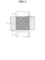
- Inkjet silver nanopaste NPS-JL (manufactured by Harima Kasei Co., Ltd.) has a pressure applying means and an electric field applying means as an ink jet recording head, and has a nozzle diameter of 25 ⁇ m, a driving frequency of 12 kHz, a number of nozzles of 128, a nozzle density of 180 dpi (dpi). 1 represents the number of dots per inch, that is, 2.54 cm), and loaded on an inkjet printing apparatus equipped with a piezo-type head, and printed on the substrate with the easy adhesion layer as shown in FIG.
- the take-out electrodes 1 and 4 in FIG. 1 are used as take-out electrodes with a silver solid portion of 1.2 cm ⁇ 5 mm.
- the metal fine line pattern 2 in FIG. 1 is in contact with the extraction electrode 1 at a metal mesh pattern portion having a line width of 50 ⁇ m and a line interval of 900 ⁇ m printed in a range of 1.2 cm ⁇ 1.2 cm.
- the blank part 3 is a 1.2 cm ⁇ 2 mm silver-free part.
- the formed fine metal wire pattern 2 was baked at 130 ° C. for 60 minutes using an oven. The height from the base material of the metal fine wire pattern 2 was 500 nm.
- the speed is adjusted so that the film thickness of the conductive polymer-containing layer of the blank portion 3 is 500 nm.
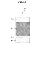
- the following conductive polymer-containing coating solution 1 was applied to the region of the conductive polymer-containing layer 5 in FIG. 2 so as to adjust and pass over the fine metal wire pattern 2 in FIG.
- region other than the metal fine wire pattern 2) of the coated sample was dried for 1 minute with warm air of 80 ° C., and the conductive polymer-containing layer 5 was wiped off with a cotton swab dipped in pure water.
- the conductive polymer containing layer 6 was provided in the area
- the structure and molecular weight were measured by 1 H-NMR (400 MHz, manufactured by JEOL Ltd.) and GPC (Waters 2695, manufactured by Waters), respectively.
- the base material is 0.7 mm thick, 4 cm ⁇ 4 cm glass substrate (Eagle EG, manufactured by Corning), silver nanopaste for inkjet NPS-J (manufactured by Harima Chemicals), and the firing conditions are 250 ° C. and 30 minutes.
- a metal pattern 2 was obtained in the same manner as the metal fine line pattern 1 except that.
- Metal fine wire pattern 3 A fine metal wire pattern 3 was obtained in the same manner as the fine metal wire pattern 1 except that the silver nanoparticle paste MDot-SLP manufactured by Mitsuboshi Belting Co., Ltd. was gravure-printed using a K303 multicoater manufactured by Matsuo Sangyo Co., Ltd.
- planar electrodes 108 to 110 were produced in the same manner except that the organic electronic device planar electrodes 102, 106, 107 were changed to the local heat treatment 2.
- planar electrode 111 for organic electronic devices (Preparation of planar electrode 111 for organic electronic devices)
- the firing condition is set to 150 ° C. for 15 minutes, and then the local heat treatment 1 is performed to perform the additional firing treatment and the local heat treatment in the same manner.
- a planar electrode 111 was produced.
- planar electrodes 112 to 114 for organic electronic devices In the surface electrode 102 for organic electronic devices, the surface for organic electronic devices was the same except that the time from the local heat treatment to the formation of the conductive polymer-containing layer was 12 hours, 24 hours, and 36 hours. The shaped electrodes 112 to 114 were produced.
- planar electrodes 120 to 122 were produced in the same manner except that the local heat treatment was changed to the following local heat treatment 4 in the planar electrodes 116, 118, and 119 for the organic electronic device.
- (Local heat treatment 4) Changed the treatment conditions for local heat treatment 3 to the following (excimer light irradiation treatment conditions) Excimer light intensity 80mW / cm 2 (172nm) 1mm distance between sample and light source Stage heating temperature 80 °C Oxygen concentration in irradiation device 0.1% Excimer irradiation time 0.2 seconds 5 times 5 times As in the case of the planar electrode 101 for organic electronic devices, it is confirmed that the direction with the fine metal wire pattern is 20 ° C. or higher than the portion without the fine metal wire pattern. did.
- planar electrodes 123 to 127 were produced in the same manner except that the local heat treatment was changed to the following local heat treatment 5 using microwave heat treatment in the planar electrodes 115 to 119 for the organic electronic device. did.
- Microwave treatment equipment Electromagnetic heating and sintering equipment (FMW-10-28, transmission frequency 28 GHz) manufactured by Fuji Radio Industry Co., Ltd. Output: 1kW Treatment time: 5 seconds In the same manner as the planar electrode 101 for organic electronic devices, it was confirmed that the direction with the fine metal wire pattern was 20 ° C. or higher than the portion without the fine metal wire pattern.
- planar electrodes 128 to 132 were prepared in the same manner except that the local heat treatment was changed to the following local heat treatment 6 using induction heat treatment in the planar electrodes 115 to 119 for the organic electronic device. .
- thermography (Thermo Tracer TH9100, NEC, manufactured by Avio Sekigaisen Technology Co., Ltd.), it was confirmed that the direction with the fine metal wire pattern was 20 ° C. or higher than the portion without the fine metal wire pattern.
- planar electrode 133 for organic electronic devices was produced similarly except having changed the local heat processing into the following local heat processing 7 using a hot-air heater process.
- Hot air heater treatment The treatment was performed at 500 ° C. for 0.01 seconds using a high heater (manufactured by Hibeck Co., Ltd.) having a slit-shaped blowout of 27 mm ⁇ 0.5 mm.
- thermography (Thermo Tracer TH9100, manufactured by NEC, Avio Sekigaisen Technology Co., Ltd.), it was confirmed that the temperature with the fine metal wire pattern was about 15 ° C. higher than the temperature of the portion without the fine metal wire pattern.
- the conductive polymer-containing coating solution 1 is the following conductive polymer-containing coating solution 6 that does not contain a water-soluble binder resin containing a structural unit represented by the general formula (I).
- the surface shape for comparative organic electronic devices was the same except that the coating speed was adjusted so that the film thickness of the conductive polymer-containing layer in the portion without the fine metal wire pattern was 50 nm without performing the local heat treatment.
- An electrode 201 was produced.
- ⁇ or more is necessary, and ⁇ or more is preferable.
- An organic EL constituent layer is formed on the obtained metal thin wire pattern of each planar electrode for organic electronic devices by the following procedure, and organic EL elements 101 to 133 and 201 corresponding to the planar electrodes for each organic electronic device are formed.
- To 205 were prepared, and the short-circuit characteristics and driving voltage of each organic EL element were evaluated.
- PEDOT-PSS CLEVIOS P AI 4083 (solid content 1.5%) (manufactured by HC Starck) was made into the same region as the conductive polymer-containing coating solution using a bar coater with a gap gap of 40 ⁇ m, and the dry film thickness was applied to a thickness of 30 nm, and unnecessary areas were wiped off in the same manner as the conductive polymer-containing coating solution. Further, heat treatment was performed at 130 ° C. for 30 minutes on a hot plate to form a hole injection layer.
- Each of the vapor deposition crucibles in a commercially available vacuum vapor deposition apparatus was filled with the optimum amount of the constituent material of each layer for device fabrication.
- a crucible made of a resistance heating material made of molybdenum or tungsten was used as the evaporation crucible.
- the deposition crucible containing compound 1 was heated by energization, and deposited at a deposition rate of 0.1 nm / second on a region with a fine metal wire pattern. A hole transport layer was provided.
- each light emitting layer was provided in the following procedures.
- the compound 2, the compound 3 and the compound 5 were deposited at a deposition rate of 0.1 nm / second so that the concentration of the compound 2 was 13% by mass and the compound 3 was 3.7% by mass.
- Co-evaporation was performed on the patterned region to form a green-red phosphorescent light emitting layer having a maximum emission wavelength of 622 nm and a thickness of 10 nm.
- the compound 4 and the compound 5 are co-deposited at a deposition rate of 0.1 nm / second in a region having a fine metal wire pattern so that the compound 4 becomes 10% by mass, and blue phosphorescence having a maximum emission wavelength of 471 nm and a thickness of 15 nm.
- a light emitting layer was formed.
- the hole blocking layer was formed by vapor-depositing the compound 6 in a film thickness of 5 nm in a region having a fine metal wire pattern.
- CsF was co-evaporated with Compound 6 so as to have a film thickness ratio of 10% in a region having a fine metal wire pattern to form an electron transport layer having a thickness of 45 nm.
- each obtained organic EL element performed subsequent evaluation under nitrogen, without taking out in air
- Drive voltage Using a source measure unit 2400 manufactured by KEITHLEY, a DC voltage was applied, a voltage required to pass a current of 3 mA to the device was determined as a drive voltage, and evaluation was performed using the following indices.
- ⁇ or more is preferable, and ⁇ ⁇ or more is more preferable.
- the method for producing a planar electrode for an organic electronic device of the present invention is to produce an electrode that provides an organic electronic device with low driving voltage and no leakage with a counter electrode while maintaining high transparency at low cost. And can be suitably used for planar electrodes for organic electronic devices.
Landscapes
- Physics & Mathematics (AREA)
- Electromagnetism (AREA)
- Electroluminescent Light Sources (AREA)
- Compositions Of Macromolecular Compounds (AREA)
Abstract
本発明の課題は、高い透明性を維持しつつ、また、駆動電圧が低く、対向電極とのリークのない有機電子デバイスを与える電極を、低コストで製造することができる有機電子デバイス用面状電極の製造方法を提供することである。本発明の有機電子デバイス用面状電極の製造方法は、基材上に金属ナノ粒子より形成された導電性の金属細線パターンと、該金属細線パターン上に少なくとも、π共役系導電性高分子とポリ陰イオンとを含んで成る導電性ポリマーと、下記一般式(I)で表される構造単位を含む水溶性バインダー樹脂とから形成された導電性ポリマー含有層とを有する有機電子デバイス用面状電極において、該金属細線パターンに局所加熱処理を施した後に前記導電性ポリマー含有層を形成することを特徴とする。 【化1】
Description
本発明は、有機電子デバイス用面状電極の製造方法に関し、更に詳しくは、高い透明性を維持しつつ、また、駆動電圧が低く、対向電極とのリークのない有機電子デバイスを与える電極を、低コストで製造することができる有機電子デバイス用面状電極の製造方法に関する。
金属ナノ粒子より形成された導電性の金属細線パターンを局所加熱により焼成することは知られている。例えば、パルス光によって焼成する例が開示されて(例えば、特許文献1参照)いる。
また、局所加熱により焼成した金属細線パターン上にPEDOT/PSS(ポリ(3,4-エチレンジオキシチオフェン)とポリスチレンスルホン酸)層を設ける例が、(例えば、非特許文献1参照)記載されている。
この技術は、優れた技術であるが、金属細線パターンの凹凸が大きいために、単純にPEDOT/PSS層を設けるだけではPEDOT/PSS層で金属パターンを覆うことができず、この電極を太陽電池や有機エレクトルミネッセンスなどの有機電子デバイスに用いた場合、対向電極と短絡してしまう。そのため、非特許文献1では、金属細線パターンを埋没する処理を施している。これには、非常に煩雑な工程が必要で改善が望まれる。あるいは、埋没処理を施さずにすませるには、PEDOT/PSS層を極端に厚くする必要があり、そうすると面電極の透過率が大きく低下して、有機電子デバイスの性能を低下させる。
導電性繊維を含む第一の透明導電層上に導電性高分子と水溶性バインダー樹脂とを含む第二の透明導電層を有する透明電極が記載されて(例えば、特許文献2参照)いる。
本発明者は、この技術を応用して、金属細線パターン上に導電性高分子と特定の水溶性バインダー樹脂とを含む透明導電層を設けることで、太陽電池や有機エレクトルミネッセンスなどの有機電子デバイスに用いた場合、対向電極との短絡を防止できることを発見した。これは、面電極の透過率を低下させることなく、かつ、金属細線パターンに複雑な埋没処理を施す必要がないことから非常に有効な技術である。
一方、金属ナノ粒子から金属細線パターンを形成することは知られており、こうした金属パターンにπ共役系導電性高分子とポリ陰イオンとを含んで成る導電性ポリマーと一般式(I)で表される構成単位を有する透明バインダーとから形成された導電性ポリマー含有層とを有する有機電子デバイス用面状電極を用いて太陽電池や有機エレクトルミネッセンスなどの有機電子デバイスを作製したところ、面状電極のシート抵抗は低いにも関わらず、デバイスの駆動電圧が高くなることが分かってきた。
こうした現象は、基材上に金属ナノ粒子より形成された導電性の金属細線パターンと該金属細線パターン上に少なくとも、π共役系導電性高分子とポリ陰イオンとを含んで成る導電性ポリマーと一般式(I)で表される構造単位を含む水溶性バインダー樹脂とから形成された導電性ポリマー含有層とを有する有機電子デバイス用面状電極において、新たに顕在化した問題であり、従って、前記特許文献1や非特許文献1には、こうした課題の示唆や解決の示唆は何らなされていない。
Organic PhotoVoltaics、Open Innovation Program ECN-Holst Centre,Netherlands、Large-area,Organic & Printed Electronics Convention、June 2,2010、Ronn Andriessen
本発明は、上記問題・状況に鑑みてなされたものであり、その解決課題は高い透明性を維持しつつ、また、駆動電圧が低く、対向電極とのリークのない有機電子デバイスを与える電極を、低コストで製造することができる有機電子デバイス用面状電極の製造方法を提供することである。
本発明の上記課題は、以下の手段により解決することができる。
1.基材上に、金属ナノ粒子より形成された導電性の金属細線パターンと、該金属細線パターン上に少なくとも、π共役系導電性高分子とポリ陰イオンとを含んで成る導電性ポリマーと、下記一般式(I)で表される構造単位を含む水溶性バインダー樹脂とから形成された導電性ポリマー含有層とを有する有機電子デバイス用面状電極の製造方法において、該金属細線パターンに局所加熱処理を施した後に前記導電性ポリマー含有層を形成することを特徴とする有機電子デバイス用面状電極の製造方法。

2.前記局所加熱処理により前記金属細線パターンと基材が20℃以上の温度差が生じるようにすることを特徴とする前記1に記載の有機電子デバイス用面状電極の製造方法。
3.前記局所加熱処理が、プラズマ処理、誘電加熱処理、エキシマ光照射処理、又はマイクロ波処理であることを特徴とする前記1又は2に記載の有機電子デバイス用面状電極の製造方法。
4.前記局所加熱処理後24時間以内に導電性ポリマー含有層を形成することを特徴とする前記1~3のいずれか1項に記載の有機電子デバイス用面状電極の製造方法。
5.前記導電性ポリマー含有層が前記一般式(I)で表される構造単位を含む水溶性バインダー樹脂を50質量%以上含有することを特徴とする前記1~4のいずれか1項に記載の有機電子デバイス用面状電極の製造方法。
6.前記基材が二軸延伸ポリエステルであることを特徴とする前記1~5のいずれか1項に記載の有機電子デバイス用面状電極の製造方法。
本発明の上記手段により、高透明で、複雑な工程を経ることなく低コストで、駆動電圧が低く、また、対向電極とのリークのない有機電子デバイスを与える有機電子デバイス用面状電極を製造することができる。
以下本発明を実施するための最良の形態について詳細に説明するが、本発明はこれらに限定されるものではない。
本発明において、金属細線パターン上に導電性ポリマー含有層を設けることで、金属細線パターンが存在しない窓部にも電気を供給することが可能となり、面状の電極として機能させている。
本発明における基材上に金属ナノ粒子より形成された導電性の金属細線パターン上にπ共役系導電性高分子とポリ陰イオンとを含んで成る導電性ポリマーと一般式(I)で表される透明バインダーとから形成された導電性ポリマー含有層を設ける技術は、一般式(I)で表される構造単位を含む水溶性バインダー樹脂に、導電性ポリマー層の導電性を向上させる効果があるために、前記導電性ポリマー含有層中に非常に多くの量を含有させることができる。そのため、透過率を低下させることなく導電性ポリマー含有層の膜厚を厚くすることができる。その結果、導電性の金属細線パターン上にこの導電性ポリマー含有層を設けることで、導電性の金属細線パターンなめらかに覆うことが可能となり、マクロ的に見ると金属細線パターンの凹凸を有するが、ミクロに見ると平滑な表面とすることができ、これによって、面電極上に機能層、対向電極を設けるような有機電子デバイスにおいても、金属細線パターンの埋没処理等の非常に煩雑な処理を必要とせず、対向電極との短絡を防止することができる。
一方、基材上に金属ナノ粒子より形成された導電性の金属細線パターンと該金属細線パターン上に少なくとも、π共役系導電性高分子とポリ陰イオンとを含んで成る導電性ポリマーと一般式(I)で表される構造単位を含む水溶性バインダー樹脂とから形成された導電性ポリマー含有層とを有する有機電子デバイス用面状電極においては、まず、該金属細線パターンから導電性ポリマー含有層に障壁なく電気を流す必要がある。一般式(I)で表される構造単位を含む水溶性バインダー樹脂を含まない導電性ポリマー単独の層である場合は、障壁なく電気を流すことができた。
しかしながら、ナノ粒子から形成された金属パターンは、表面に分散剤等が残りやすい。こうした剤が残ってもパターンが形成されている面内方向の導通は得られるが、本発明のように導電性ポリマー含有層に一般式(I)で表される構造単位を含む水溶性バインダー樹脂を含む場合、金属細線パターンから導電性ポリマー含有層に電流を流す場合に駆動電圧が上昇することがあった。これは、詳細は良く分かっていないが、π共役系導電性高分子とポリ陰イオンとを含んで成る導電性ポリマーよりも一般式(I)で表される構造単位を含む水溶性バインダー樹脂の方が残存した分散剤等とインタラクションが強いために、該金属細線パターンと導電性ポリマー含有層間に導電性のない分散剤と一般式(I)で表される構造単位を含む水溶性バインダー樹脂からなる絶縁膜が薄く形成されるためではないかと考えている。
あるいは、通常の加熱焼成をした金属細線パターンの表面では、π共役系導電性高分子とポリ陰イオンとを含んで成る導電性ポリマーよりも一般式(I)で表される構造単位を含む水溶性バインダー樹脂とより親和性が高く、一般式(I)で表される構造単位を含む水溶性バインダー樹脂からなる絶縁膜が薄く形成されるためではないかと考えている。
本発明においては、こうした課題に対して、金属細線パターンに局所加熱処理を施した後に前記導電性ポリマー含有層を形成することで、駆動電圧の上昇なく、有機電子デバイスに適用できることを見いだして、本発明に至った。
これは、金属細線パターンに直接エネルギーを伝える処理をすることが、金属細線パターン上に残存した分散剤を除去するのに有効であり、その結果、該金属細線パターン上にπ共役系導電性高分子とポリ陰イオンとを含んで成る導電性ポリマーと一般式(I)で表される構造単位を含む水溶性バインダー樹脂とを少なくとも含有する導電性ポリマー含有層を設けても、該金属細線パターンから導電性ポリマー含有層への通電阻害を起こさなくなったと考えている。あるいは、金属細線パターンに直接エネルギーを伝える処理をすることで金属細線パターンの表面状態が代わり、一般式(I)で表される構造単位を含む水溶性バインダー樹脂よりも、π共役系導電性高分子とポリ陰イオンとを含んで成る導電性ポリマーとのインタラクションとの親和性の方が高くなり、該金属細線パターンから導電性ポリマー含有層への通電阻害を起こさなくなったとも考えている。
以下、本発明の好ましい実施形態について記載するが、これらに限定されない。
〔金属細線パターン〕
本発明の有機電子デバイス用面状電極において、まず、基材上に金属ナノ粒子を用いて導電性の金属細線パターンを形成する。
本発明の有機電子デバイス用面状電極において、まず、基材上に金属ナノ粒子を用いて導電性の金属細線パターンを形成する。
金属ナノ粒子は、金、銀、銅、白金、パラジウム、ニッケル及びアルミニウムからなる金属元素の群から選択される単体金属種、又は、金、銀、銅、白金、パラジウム、ニッケル及びアルミニウムからなる金属元素の群から選択される二種以上の金属種からなる合金を挙げることができる。
金属ナノ粒子の粒径は1nm以上100nm以下であり、50nm以下であることがより好ましく、30nm以下であることがより好ましい。
金属ナノ粒子は、慣用の方法、例えば、金属ナノ粒子に対応する金属化合物を、保護コロイド及び還元剤の存在下、溶媒中で還元することにより調製できる。
金属ナノ粒子に対応する金属化合物は、例えば、金属酸化物、金属水酸化物、金属硫化物、金属ハロゲン化物、金属酸塩[金属無機酸塩(硫酸塩、硝酸塩、過塩素酸塩等のオキソ酸塩等)、金属有機酸塩(酢酸塩等)等]等であってもよい。なお、金属塩の形態は、単塩、複塩又は錯塩のいずれであってもよく、多量体(例えば、2量体)等であってもよい。これらの金属化合物は単独で又は二種以上組み合わせて使用できる。これらの金属化合物のうち、金属ハロゲン化物、金属酸塩[金属無機酸塩(硫酸塩、硝酸塩、過塩素酸塩等のオキソ酸塩等)、金属有機酸塩(酢酸塩等)等]等を使用する場合が多い。なお、これらの金属化合物は、溶媒に溶解又は分散させて(例えば、水溶液等の水系溶媒の溶液の形態で)用いてもよい。
還元剤としては、慣用の成分、例えば、水素化ホウ素ナトリウム類(水素化ホウ素ナトリウム、シアノ水素化ホウ素ナトリウム、水素化トリエチルホウ素ナトリウム等)、水素化アルミニウムリチウム、次亜リン酸又はその塩(ナトリウム塩等)、ボラン類(ジボラン、ジメチルアミンボラン等)、ヒドラジン類(ヒドラジン等)、ホルマリン、アミン類[例えば、メチルアミノエタノール、ジメチルアミノエタノール(2-(ジメチルアミノ)エタノール)、エタノールアミン、ジエタノールアミン、トリエタノールアミン、メチルジエタノールアミン、プロパノールアミン、2-(3-アミノプロピルアミノ)エタノール、ブタノールアミン、ヘキサノールアミン、ジメチルアミノプロパノール等のアルカノールアミン類、有機酸(クエン酸、酒石酸、アスコルビン酸等)等が例示できる。これらの還元剤は単独で又は二種以上組み合わせて使用できる。
還元剤の使用量は、金属原子換算で前記金属化合物1当量(又は1モル)に対して、1~30モル(例えば、1.2~20モル)、好ましくは1.5~15モル、さらに好ましくは2~10モル程度であってもよく、通常1~5モル程度であってもよい。
還元反応は、慣用の方法、例えば、10~75℃(例えば、15~50℃、好ましくは20~35℃)程度で行うことができる。反応系の雰囲気は、空気、不活性ガス(窒素ガス等)であってもよく、還元性ガス(水素ガス等)を含む雰囲気であってもよい。また、反応は、通常、攪拌下で(又は攪拌しながら)行ってもよい。
なお、反応溶媒としては、最終的な金属ナノ粒子インクを構成する後述の分散媒であってもよく、金属ナノ粒子インクを構成する分散媒とは異なる溶媒であってもよく、これらの混合溶媒であってもよい。反応溶媒としては、前記保護コロイドの種類等に応じて選択でき、例えば、保護コロイドが水溶性化合物である場合には、水等の極性溶媒で反応溶媒を構成することが多く、疎水性化合物である場合には疎水性溶媒で反応溶媒を構成することが多い。
反応溶媒は、前記分散媒の他、疎水性溶媒[例えば、炭化水素類(例えば、ヘキサン、ヘプタン、トリメチルペンタン、オクタン、デカン、ドデカン、テトラデカン等の脂肪族炭化水素類;シクロヘキサン等の脂環式炭化水素類;トルエン、キシレン等の芳香族炭化水素類;ジクロロメタン、トリクロロエタン等のハロゲン化炭化水素類等)、エステル類(酢酸メチル、酢酸エチル等)、ケトン類(メチルエチルケトン、メチルイソブチルケトン等)、エーテル類(ジエチルエーテル、ジプロピルエーテル等)等]、極性溶媒[水、アルコール類(メタノール、エタノール、プロパノール、イソプロパノール、ブタノール等のC1-4アルカノール等)、脂肪族多価アルコール類(エチレングリコール、ポリエチレングリコール、グリセリン等)、ケトン類(アセトン等)、エーテル類(ジオキサン、テトラヒドロフラン等)、有機カルボン酸類(酢酸等)等]等が挙げられる。これらの溶媒は単独で又は二種以上組み合わせてもよい。反応溶媒は、通常、少なくとも疎水性溶媒(前記分散媒でない疎水性溶媒)で構成してもよい。
なお、反応溶媒中の前記金属化合物の濃度は、金属の質量換算で、例えば、5質量%以上(例えば、6~50質量%)、好ましくは8質量%以上(例えば、9~40質量%)、さらに好ましくは10質量%以上(例えば、12~30質量%)、通常5~30質量%程度の高濃度であってもよい。
なお、反応溶媒の種類等に応じて反応系のpHを調整してもよい。
pH調整は、慣用の方法、例えば、酸(塩酸、硫酸、硝酸、リン酸、過塩素酸等の無機酸、ギ酸、酢酸、プロピオン酸、安息香酸等の有機酸)、アルカリ[水酸化ナトリウム、アンモニア等の無機塩基、アミン類(例えば、アルキルアミン、アルカノールアミン等の第三級アミン類等の有機塩基)等の塩基類]を用いて行うことができる。
上記のような反応(還元反応)により、反応溶媒に金属コロイド粒子(A)が分散した分散液の形態で金属コロイド粒子(A)を調製することができる。なお、還元反応の終了後、必要に応じて、反応混合液を慣用の方法(例えば、遠心分離、メンブレンフィルタ、限外ろ過等のろ過処理等)で精製してもよい。
そして、金属ナノ粒子インクは、前記反応溶媒として前記分散媒を含む溶媒を用いた場合には、分散液から不要な溶媒成分を濃縮して調製することもできるが、通常、このような分散液から分離した前記金属コロイド粒子(A)を前記分散媒に分散(再分散)させることにより調製できる。
分散液からの金属コロイド粒子(A)の分離は、慣用の方法、例えば、分散液から反応溶媒を分離除去することにより行うことができる。反応溶媒の除去は、慣用の濃縮操作等を利用できる。なお、前記反応溶媒の除去は、反応溶媒と前記分散媒との沸点差を利用して、分散媒の存在下で行ってもよい(すなわち、反応溶媒の除去と分散媒への分散を同一の系で行ってもよい)。例えば、前記分散液に前記分散媒を混合した混合物から前記反応溶媒を除去してもよい。
分散媒の使用量としては、所望の粘度となるように適宜調整でき、前記と同様の範囲から適宜選択してもよい。なお、分散媒に加えて他の溶媒を混合し、他の溶媒を除去することにより粘度調整を行ってもよい。
金属ナノ粒子を用いるには、有機保護コロイドで被覆した状態で使用することが好ましい。この有機保護コロイドとしては、分解温度あるいは沸点が70~250℃の範囲のものを用いることが好ましい。この分解温度あるいは沸点とは、分解温度と沸点のうち低い方の温度をいうものである。そして有機保護コロイドの分解温度あるいは沸点が250℃以内であると、低温の熱処理で有機保護コロイドを分解あるいは蒸発させることができ、低温焼成を容易に行うことができる。また有機保護コロイドの分解温度あるいは沸点が70℃以上であると、銀ペーストを保存する間に有機保護コロイドが分解あるいは蒸発する恐れがなく、銀ペーストの保存安定性が良好である。
また有機保護コロイドとしては、炭素数3~18の炭化水素類を用いるのが好ましい。炭素数が18以下であると、分解温度あるいは沸点が高くなって、低温の熱処理で有機保護コロイドを分解あるいは蒸発させることができなくなる恐れがなく、また炭素数が3以上であると、分解温度あるいは沸点が低くなり過ぎて、銀ペーストの保存安定性に問題が生じる恐れがない。
上記のような条件満たす有機保護コロイドとしては、特に限定されるものではないが、オクチルアミン(沸点178~179℃)、6-メチル-2-ヘプチルアミン(沸点154~156℃)、ジブチルアミン(沸点160~162℃)、ヘキシルアミン(沸点130~132℃)、ジプロピルアミン(沸点105℃)、ジイソプロピルアミン(沸点83~84℃)、ブチルアミン(沸点76~78℃)、ステアリン酸(沸点232℃;19.95hPa)、パルミチン酸(沸点271.4℃;133hPa)、ミリスチン酸(沸点250℃;133hPa)、ラウリン酸(沸点131℃;1.3hPa)、オクタン酸(沸点238℃)、ヘキサン酸(沸点206℃)、酪酸(沸点162~165℃)、オクタデカジエン酸(229~230℃)等を例示することができ、これらを一種単独で用いる他、二種以上を併用することもできるものである。
これらのなかでも、有機保護コロイドとしては、アミン(アミノ基)を含むものが特に好ましい。アミン類を含むことによって、有機保護コロイドで金属ナノ粒子を保護する効果を高く得ることができるものであり、また焼成の際に有機保護コロイドが残留することがなくなり、有機物残渣で比抵抗に悪影響を及ぼすことを防ぐことができるものである。
有機保護コロイドで金属ナノ粒子の表面を被覆する方法は、任意の方法を採用することができるが、例えば、金属ナノ粒子を調製する際に有機保護コロイドを共存させることによって、金属ナノ粒子の表面を有機保護コロイドで容易に被覆することができるものである。また有機保護コロイドによる金属ナノ粒子の被覆量は、特に限定されるものではないが、金属ナノ粒子100質量部に対して1~40質量部の範囲に設定するのが望ましい。
分散媒についても、分解温度あるいは沸点が70~250℃の範囲のものを用いることが好ましい。この分解温度あるいは沸点とは、分解温度と沸点のうち低い方の温度をいうものである。そして分散媒の分解温度あるいは沸点が250℃以内であると、低温の熱処理で分散媒を分解あるいは蒸発させることができ、低温焼成を容易に行うことができる。また分散媒の分解温度あるいは沸点が70℃以上であると、銀ペーストを保存する間に分散媒が分解あるいは蒸発する恐れがなく、銀ペーストの保存安定性が良好である。
また分散媒としては、炭素数3~18の炭化水素類を用いるのが好ましい。炭素数が18以下であると、分解温度あるいは沸点が高くなって、低温の熱処理で分散媒を分解あるいは蒸発させることができなくなる恐れがなく、また炭素数が3以上であると、分解温度あるいは沸点が低くなり過ぎて、銀ペーストの保存安定性に問題が生じるおそれがない。
このような分散媒としては、特に限定されるものではないが、ミスチルアルコール(沸点167℃;20hPa)、ラウリルアルコール(沸点258~265℃)、ウンデカノール(沸点129~131℃;16hPa)、デカノール(沸点220~235℃)、ノナノール(沸点214~216℃)、オクタノール(沸点188~198℃)等を例示することができ、これらを一種単独で用いる他、二種以上を併用することもできるものである。
これらの中でも、分散媒としてデカノールを用いることが特に好ましい。分散媒としてデカノールを用いることによって、スクリーン印刷等で描画するのに適した銀ペーストを得ることができるものである。
本発明に係る金属ナノ粒子インクは、有機保護コロイドで覆われた金属ナノ粒子や分散媒の他に、基材との密着性を向上する目的でバインダーを含んでいても良い。ただし、金属ナノ粒子を被覆する有機保護コロイドはバインダーとしての役割も果たす場合があるので、バインダーを配合することは必須ではなく、有機保護コロイドで覆われた金属ナノ粒子や分散媒のみで金属ナノ粒子インクを調製することも可能である。
金属ナノ粒子インク中の分散媒の量は、金属ナノ粒子インクの塗布方法によって異なるものであり、塗布方法に応じた粘度や流動性を得ることができるように、適宜設定されるものである。
このようにして調製した金属ナノ粒子インクを、グラビア印刷、フレキソ印刷、スクリーン印刷、インクジェット印刷等の従来公知の各種印刷法により所望の形状で基板等の表面に印刷し、金属細線パターンを形成する。
パターンとは、開口部を有する模様であり、パターンの形状としては、例えば開口部の形が三角形、正方形、長方形、菱形、平行四辺形、台形等の四角形、(正)六角形、(正)八角形等多角形を組み合わせた幾何学図形からなるメッシュ状のパターンが挙げられる。
また、複数の平行なラインからなるストライプ状に金属組成物が存在する形状でもよい。
本発明に係る金属細線パターンの形状は、金属組成物が編み目状に連続しているネットワーク構造を有する形状であることが好ましい態様である。
パターンの金属組成物の存在する部分の形の、線幅、線間隔、高さは特に制限はなく、目標とするシート抵抗やパターンの形成方法に応じて適宜選択できるが、例えば、線幅10~200μm、線間隔が0.1から10mm、高さが0.1~10μmとすることが好ましい。
金属細線パターンは、導電性を発現させるために、焼成処理を施す。熱処理の方法としては、従来一般に行われるオーブンによる加熱やホットプレートによる加熱を用いることができる。加熱の条件は金属ナノ粒子インクによっても異なるが、通常200℃から500℃で、1分から60分程度の焼成を行う。低温でも焼成できるインクも提案されており、そうしたインクでは、100℃から200℃で1分から60分程度の焼成を行う。
また、焼成処理は後述の局所加熱処理を用いても良く、オーブンによる加熱やホットプレートによる加熱と局所加熱処理を併用して施してもよい。
(局所加熱)
従来、加熱処理としては、ある空間を一定の温度に保ったところに加熱したいサンプルを分単位以上の比較的長時間、一定の時間放置する方法(オーブン、焼成炉など)や、一定の温度に保った金属板に加熱したいサンプルを分単位以上の比較的長時間、一定時間放置する方法(ホットプレートなど)が行われている。こうした処理は、基材や金属細線パターンなど、サンプル全体を一定の温度に保って処理される。
従来、加熱処理としては、ある空間を一定の温度に保ったところに加熱したいサンプルを分単位以上の比較的長時間、一定の時間放置する方法(オーブン、焼成炉など)や、一定の温度に保った金属板に加熱したいサンプルを分単位以上の比較的長時間、一定時間放置する方法(ホットプレートなど)が行われている。こうした処理は、基材や金属細線パターンなど、サンプル全体を一定の温度に保って処理される。
本発明においては、導電性ポリマー含有層を形成する前に、前述の金属細線パターンに局所加熱処理を施す。局所加熱処理は前述の金属細線パターンの焼成処理後に行うことが好ましいが、焼成処理と兼ねて行っても良い。局所加熱処理とは、エネルギー照射に対する金属細線パターンと、それ以外の基材などの部材との吸収効率の差を利用したり、あるいは、短時間に高エネルギーを、金属細線パターンを含む表面に施すことにより、熱の伝搬で基材の温度が上がる前に金属細線パターン部を高温にすることを利用したりすることで、金属細線パターン部をそれ以外の基材などの部材よりも高温にする処理である。こうした局所加熱処理は、一回の処理時間は10秒以下、好ましくは1秒以下のごく短時間の処理であり、こうした処理を繰り返し実施することも好ましい。
本発明において、局所加熱処理により、金属細線パターン部はそれ以外の基材などの部材よりも高温にすることが好ましく、特に20℃以上高温にすることが好ましく、より好ましくは30℃以上高温にすることが好ましい。こうした温度差を生じるには、金属細線パターン部が短時間に強いエネルギー照射を受ける必要があり、結果としてそのエネルギー処理により金属細線パターン部の表面が改質されて本発明の効果を生じていると考えている。こうした温度測定はサーモグラフィを用いて、金属細線パターン部と基材部の温度差を測定することにより求めることができる。熱電対が処理による影響を受けないような処理では、金属細線パターン部と基材部とのそれぞれに熱電対を接続して温度をモニタすることで求めることもできる。
本発明では、上記測定法で金属細線パターンと基材が20℃以上の温度差が生じるようにすることが好ましい。
このような処理として、例えば、プラズマ処理、誘電加熱処理、エキシマ光照射処理、紫外線処理、マイクロ波処理、赤外ヒーター処理、熱風ヒーター処理などを挙げることができる。中でも、プラズマ処理、誘電加熱処理、エキシマ光照射処理、又はマイクロ波処理が好ましい。
(プラズマ処理)
プラズマ処理としては、真空系を利用したプラズマ処理、大気圧近傍下で行う大気圧プラズマ処理のいずれも用いることができるが、大気圧近傍下で行う大気圧プラズマ処理は、真空プロセスが不要で工程が簡素化できるメリットがある。
プラズマ処理としては、真空系を利用したプラズマ処理、大気圧近傍下で行う大気圧プラズマ処理のいずれも用いることができるが、大気圧近傍下で行う大気圧プラズマ処理は、真空プロセスが不要で工程が簡素化できるメリットがある。
プラズマ処理は、高温のプラズマガスから最表面にのみ強くエネルギーを受けるため、厚みのある基材部分よりも、最表面の金属細線パターン部は瞬時に加熱されることで効果が出て好ましい。
(大気圧プラズマ処理)
大気圧プラズマ処理は大気圧近傍の圧力下でプラズマを発生させ、非処理材表面を処理する処理方法であり、公知のプラズマ放電処理装置を用い公知の方法で処理できる。
大気圧プラズマ処理は大気圧近傍の圧力下でプラズマを発生させ、非処理材表面を処理する処理方法であり、公知のプラズマ放電処理装置を用い公知の方法で処理できる。
大気圧プラズマ処理には、被処理材をはさむように対向配置された電極間に高周波電力を加えて、供給ガスをプラズマ化するプラナー方式と、反応ガスを高周波電圧が加えられた電極の間を通してプラズマ化するダウンストリーム方式があるが、本発明ではいずれの方式も利用できる。
電源としては、特に限定はないが、パール工業製高周波電源(200kHz)、パール工業製高周波電源(800kHz)、日本電子製高周波電源(13.56MHz)、パール工業製高周波電源(150MHz)等が使用できる。
電源より印加される電圧の値は適宜決定されるが、例えば、電圧が0.5~10kV程度で、電源周波数は100kHzを越えて150MHz以下に調整される。ここで電源の印加法に関しては、連続モードと呼ばれる連続サイン波状の連続発振モードとパルスモードと呼ばれるON/OFFを断続的に行う断続発振モードのどちらを採用してもよい。
電力の下限値は、好ましくは1.2W/cm2以上であり、上限値としては、好ましくは50W/cm2以下、さらに好ましくは20W/cm2以下である。なお、電極における電圧の印加面積(/cm2)は、放電が起こる範囲の面積のことを指す。
本発明においては、このようなハイパワーの電圧を印加して、均一なグロー放電状態を保つことができる電極をプラズマ放電処理装置に採用する必要がある。
このような電極としては、金属母材上に誘電体を被覆したものであることが好ましい。少なくとも対向する印加電極とアース電極の片側に誘電体を被覆すること、さらに好ましくは、対向する印加電極とアース電極の両方に誘電体を被覆することである。誘電体としては、比誘電率が6~45の無機物であることが好ましく、このような誘電体としては、アルミナ、窒化珪素等のセラミックス、あるいは、ケイ酸塩系ガラス、ホウ酸塩系ガラス等のガラスライニング材等が挙げられる。
放電電極間の距離は、均一な放電を行う観点から0.5~20mmが好ましく、より好ましくは0.5~5mmであり、特に好ましくは1~3mmである。
なお、大気圧近傍とは、20~110kPaの圧力を表すが、本発明に記載の効果を好ましく得るためには、93~104kPaが好ましい。
本発明において使用するガスは、基本的に、不活性ガスと有機フッ素化合物等の反応性ガスの混合ガスである。反応性ガスは、混合ガスに対し0.01~10体積%含有させることが好ましい。
上記不活性ガスとは、周期表の第18属元素、具体的には、ヘリウム、ネオン、アルゴン、クリプトン、キセノン、ラドン等が挙げられるが、本発明に記載の効果を得るためには、ヘリウム、アルゴンが好ましく用いられる。
また、混合ガス中に酸素、オゾン、過酸化水素、二酸化炭素、一酸化炭素、水素、窒素から選択される成分を0.01~5体積%含有させることにより、反応を促進させることができる。
(紫外線処理)
紫外線照射処理としては、高圧水銀ランプ、低圧水銀ランプ、キセノンランプ、エキシマ光による処理などを挙げることができ、例えば、前述の特許文献2に記載のようなエキシマ光をパルス照射することも好ましく用いることができる。さらに、エキシマ光照射処理は短時間で強いエネルギーを照射することができ、本発明において、好ましく用いることができる。エキシマ光照射処理は、短時間で強いエネルギーを受けるために、基材への熱が拡散する前に金属細線パターン部が高温となる。
紫外線照射処理としては、高圧水銀ランプ、低圧水銀ランプ、キセノンランプ、エキシマ光による処理などを挙げることができ、例えば、前述の特許文献2に記載のようなエキシマ光をパルス照射することも好ましく用いることができる。さらに、エキシマ光照射処理は短時間で強いエネルギーを照射することができ、本発明において、好ましく用いることができる。エキシマ光照射処理は、短時間で強いエネルギーを受けるために、基材への熱が拡散する前に金属細線パターン部が高温となる。
〈エキシマ光照射処理〉
Xe、Kr、Ar、Ne等の希ガスの原子は化学的に結合して分子を作らないため、不活性ガスと呼ばれる。しかし、放電等によりエネルギーを得た希ガスの原子(励起原子)は、他の原子と結合して分子を作ることができる。希ガスがキセノンの場合には
e+Xe→e+Xe*
Xe*+Xe+Xe→Xe2 *+Xe
となり、励起されたエキシマ分子であるXe2 *が基底状態に遷移するときに172nmのエキシマ光を発光する。他にも、例えば、222nm、308nmの単一波長の発光が知られている。本発明においては、処理効率の点から172nmのエキシマ光処理がより好ましい。エキシマランプの特徴としては、放射が一つの波長に集中し、必要な光以外がほとんど放射されないので効率が高いことが挙げられる。
Xe、Kr、Ar、Ne等の希ガスの原子は化学的に結合して分子を作らないため、不活性ガスと呼ばれる。しかし、放電等によりエネルギーを得た希ガスの原子(励起原子)は、他の原子と結合して分子を作ることができる。希ガスがキセノンの場合には
e+Xe→e+Xe*
Xe*+Xe+Xe→Xe2 *+Xe
となり、励起されたエキシマ分子であるXe2 *が基底状態に遷移するときに172nmのエキシマ光を発光する。他にも、例えば、222nm、308nmの単一波長の発光が知られている。本発明においては、処理効率の点から172nmのエキシマ光処理がより好ましい。エキシマランプの特徴としては、放射が一つの波長に集中し、必要な光以外がほとんど放射されないので効率が高いことが挙げられる。
また、余分な光が放射されないので、対象物の温度を低く保つことができる。さらには始動・再始動に時間を要さないので、瞬時の点灯点滅が可能である。
エキシマ発光を得るには、誘電体バリア放電を用いる方法が知られている。誘電体バリア放電とは、両電極間に誘電体(エキシマランプの場合は透明石英)を介してガス空間を配し、電極に数10kHzの高周波高電圧を印加することによりガス空間に生じる、雷に似た非常に細いmicro dischargeと呼ばれる放電で、micro dischargeのストリーマが管壁(誘電体)に達すると誘電体表面に電荷が溜まるため、micro dischargeは消滅する。このmicro dischargeが管壁全体に広がり、生成・消滅を繰り返している放電である。このため肉眼でも分かる光のチラツキを生じる。また、非常に温度の高いストリーマが局所的に直接管壁に達するため、管壁の劣化を早める可能性もある。
効率よくエキシマ発光を得る方法としては、誘電体バリア放電以外に無電極電界放電でも可能である。容量性結合による無電極電界放電で、別名RF放電とも呼ばれる。ランプと電極及びその配置は基本的には誘電体バリア放電と同じでよいが、両極間に印加される高周波は数MHzで点灯される。無電極電界放電はこのように空間的にまた時間的に一様な放電が得られるため、チラツキがない長寿命のランプが得られる。
誘電体バリア放電の場合はmicro dischargeが電極間のみで生じるため、放電空間全体で放電を行わせるには外側の電極は外表面全体を覆い、かつ外部に光を取り出すために光を透過するものでなければならない。このため細い金属線を網状にした電極が用いられる。この電極は光を遮らないようにできるだけ細い線が用いられるため、酸素雰囲気中では真空紫外光により発生するオゾン等により損傷しやすい。
これを防ぐためにはランプの周囲、すなわち照射装置内を窒素等の不活性ガスの雰囲気にし、合成石英の窓を設けて照射光を取り出す必要が生じる。合成石英の窓は高価な消耗品であるばかりでなく、光の損失も生じる。
二重円筒型ランプは外径が25mm程度であるため、ランプ軸の直下とランプ側面では照射面までの距離の差が無視できず、照度に大きな差を生じる。したがって仮にランプを密着して並べても、一様な照度分布が得られない。合成石英の窓を設けた照射装置にすれば酸素雰囲気中の距離を一様にでき、一様な照度分布が得られる。
無電極電界放電を用いた場合には外部電極を網状にする必要はない。ランプ外面の一部に外部電極を設けるだけでグロー放電は放電空間全体に広がる。外部電極には、通常アルミのブロックで作られた光の反射板を兼ねた電極がランプ背面に使用される。しかし、ランプの外径は誘電体バリア放電の場合と同様に大きいため、一様な照度分布にするためには合成石英が必要となる。
細管エキシマランプの最大の特徴は構造がシンプルなことである。石英管の両端を閉じ、内部にエキシマ発光を行うためのガスを封入しているだけである。したがって、非常に安価な光源を提供できる。
二重円筒型ランプは内外管の両端を接続して閉じる加工をしているため、細管ランプに比べ取扱いや輸送で破損しやすい。細管ランプの管の外径は6~12mm程度で、余り太いと始動に高い電圧が必要になる。
放電の形態は誘電体バリア放電でも無電極電界放電のいずれでも使用できる。電極の形状はランプに接する面が平面であってもよいが、ランプの曲面に合わせた形状にすればランプをしっかり固定できるとともに、電極がランプに密着することにより放電がより安定する。また、アルミで曲面を鏡面にすれば光の反射板にもなる。
Xeエキシマランプは、波長の短い172nmの紫外線を単一波長で放射することから発光効率に優れている。この光は、酸素の吸収係数が大きいため、ラジカルな酸素原子種やオゾンを高濃度で発生することができ、また、有機物の結合を解離させる能力が高い。この活性酸素やオゾンと紫外線放射が持つ高いエネルギーによって、短時間で極表面部分のみを効率的に除去できる。
エキシマ光の照射条件としては、エキシマ光の強度は1~200mW/cm2であることが好ましい。照射時間は0.5~10秒であることが好ましい。
エキシマ光強度と照射時間の積を積算強度とした時、積算強度が5~1000mJ/cm2であることが好ましく、50~500mJ/cm2であることがより好ましい。積算強度が5J/cm2よりも少ないと効果が小さく、1000mJ/cm2を超えると処理によるダメージが大きくなってくる。
また、エキシマ光照射処理を施す際の酸素濃度は0.1~10質量%であることが好ましく、0.5~5質量%であることがより好ましい。
(マイクロ波)
局所加熱としてはマイクロ波照射も利用できる。マイクロ波照射を利用してもよい。マイクロ波としては、一般の電子レンジに採用されている汎用的な周波数2.45GHzのマイクロ波であっても良いが、この場合は、金属細線パターンの一部でアーク放電が発生し、部分的な異常加熱が生じたり発火したりして、電極層やフィルム基板を著しく損傷してしまうことがある。こうした場合は、例えば、特開2006-60064号公報記載のような放電を防止する手法を合わせて用いることが好ましい。あるいは、10GHz以上のマイクロ波であれば、放電なく処理することが可能であり、放電防止手法を用いる必要がないことから、周波数10~60GHzのマイクロ波照射を施して加熱処理を行うことがより好ましい。
局所加熱としてはマイクロ波照射も利用できる。マイクロ波照射を利用してもよい。マイクロ波としては、一般の電子レンジに採用されている汎用的な周波数2.45GHzのマイクロ波であっても良いが、この場合は、金属細線パターンの一部でアーク放電が発生し、部分的な異常加熱が生じたり発火したりして、電極層やフィルム基板を著しく損傷してしまうことがある。こうした場合は、例えば、特開2006-60064号公報記載のような放電を防止する手法を合わせて用いることが好ましい。あるいは、10GHz以上のマイクロ波であれば、放電なく処理することが可能であり、放電防止手法を用いる必要がないことから、周波数10~60GHzのマイクロ波照射を施して加熱処理を行うことがより好ましい。
マイクロ波による加熱は、電波出力、照射時間等の条件を適宜定めることができる。電波出力は、0.01~10kW、好ましくは0.1~5kWの範囲である。また、照射時間は、1秒~60分、好ましくは2秒~30分の範囲である。
マイクロ波装置としては、例えば、富士電波工業株式会社製の電磁波加熱焼結装置(FMW-10-28、発信周波数28GHz、電波出力~10kW)等が使用できる。
また、マイクロ波を照射して加熱する際に、必要に応じて透明支持体の裏面(導電性金属層及び導電性ポリマー層を形成しない側)に鉄、ステンレス、銅等の熱伝導性のよい金属板、ガラス等の無機板等を設置して、透明支持体にかかる熱を放熱させることが可能な放熱板等を設けておくことができる。
(誘導加熱処理)
誘導加熱処理は、コイル形状の導体中心への永久磁石の入れ抜きに応じて磁界が変化し、導体に電流が流れる現象である電磁気誘導作用を用いて、コイルの磁場内にある加熱物内に電流を誘導させて加熱する方式である。この誘導電流は、物体内に電流が渦を巻きながら流れる渦電流により生じ、ヒステリシス損失によるジュール熱を発生して極めて短時間に発熱が起こる。このように発生された熱で加熱する処理である。
誘導加熱処理は、コイル形状の導体中心への永久磁石の入れ抜きに応じて磁界が変化し、導体に電流が流れる現象である電磁気誘導作用を用いて、コイルの磁場内にある加熱物内に電流を誘導させて加熱する方式である。この誘導電流は、物体内に電流が渦を巻きながら流れる渦電流により生じ、ヒステリシス損失によるジュール熱を発生して極めて短時間に発熱が起こる。このように発生された熱で加熱する処理である。
誘導加熱は10~900kHzの周波数で行われることが好ましく、さらに好ましくは、100~700kHz周波数で行うことである。10kHzより小さい周波数を用いると、周波数による熱の発生が弱いので好ましくないし、900kHzを超過する周波数を用いると、表皮効果による表面極小加熱のため好ましくない。
(熱風ヒーター処理)
さらには、0.1mmから10mmの吹き出し穴やスリット状の吹き出し口を有するノズルを用いて300℃から1000℃の高温の熱風を1秒未満、より好ましくは0.1秒未満のごく短時間照射する熱風ヒーター処理も利用することができる。例えば、ハイベック社製のハイヒーター装置を用いて処理することができる。
さらには、0.1mmから10mmの吹き出し穴やスリット状の吹き出し口を有するノズルを用いて300℃から1000℃の高温の熱風を1秒未満、より好ましくは0.1秒未満のごく短時間照射する熱風ヒーター処理も利用することができる。例えば、ハイベック社製のハイヒーター装置を用いて処理することができる。
〔導電性ポリマー含有層〕
本発明に係る導電性ポリマー含有層は、少なくとも、π共役系導電性高分子とポリ陰イオンとを含んで成る導電性ポリマーと一般式(I)で表される構造単位を含む水溶性バインダー樹脂とから形成される。
本発明に係る導電性ポリマー含有層は、少なくとも、π共役系導電性高分子とポリ陰イオンとを含んで成る導電性ポリマーと一般式(I)で表される構造単位を含む水溶性バインダー樹脂とから形成される。
本発明に係る導電性ポリマー含有層の形成には、グラビア印刷法、フレキソ印刷法、スクリーン印刷法、インクジェット印刷等の各種印刷方法に加えて、ロールコート法、バーコート法、ディップコーティング法、スピンコーティング法、キャスティング法、ダイコート法、ブレードコート法、カーテンコート法、スプレーコート法、ドクターコート法等の各種塗布法を用いることができる。
また、本発明に係る導電性ポリマー含有層は、本発明に係る金属細線パターンの局所加熱処理後24時間以内に形成されることが好ましい。24時間以内であれば、前述の金属細線パターン部表面の改質効果は減少することがない。
〈導電性ポリマー〉
本発明に係る導電性ポリマーは、π共役系導電性高分子とポリ陰イオンとを含んでなる。こうした導電性ポリマーは、後述するπ共役系導電性高分子を形成する前駆体モノマーを、適切な酸化剤と酸化触媒と後述のポリ陰イオンの存在下で化学酸化重合することによって容易に製造できる。
本発明に係る導電性ポリマーは、π共役系導電性高分子とポリ陰イオンとを含んでなる。こうした導電性ポリマーは、後述するπ共役系導電性高分子を形成する前駆体モノマーを、適切な酸化剤と酸化触媒と後述のポリ陰イオンの存在下で化学酸化重合することによって容易に製造できる。
(π共役系導電性高分子)
本発明に用いるπ共役系導電性高分子としては、特に限定されず、ポリチオフェン(基本のポリチオフェンを含む、以下同様)類、ポリピロール類、ポリインドール類、ポリカルバゾール類、ポリアニリン類、ポリアセチレン類、ポリフラン類、ポリパラフェニレンビニレン類、ポリアズレン類、ポリパラフェニレン類、ポリパラフェニレンサルファイド類、ポリイソチアナフテン類、ポリチアジル類、の鎖状導電性ポリマーを利用することができる。中でも、導電性、透明性、安定性等の観点、及び、金属ナノ粒子への吸着のしやすさから、ポリチオフェン類やポリアニリン類が好ましい。ポリエチレンジオキシチオフェンが最も好ましい。
本発明に用いるπ共役系導電性高分子としては、特に限定されず、ポリチオフェン(基本のポリチオフェンを含む、以下同様)類、ポリピロール類、ポリインドール類、ポリカルバゾール類、ポリアニリン類、ポリアセチレン類、ポリフラン類、ポリパラフェニレンビニレン類、ポリアズレン類、ポリパラフェニレン類、ポリパラフェニレンサルファイド類、ポリイソチアナフテン類、ポリチアジル類、の鎖状導電性ポリマーを利用することができる。中でも、導電性、透明性、安定性等の観点、及び、金属ナノ粒子への吸着のしやすさから、ポリチオフェン類やポリアニリン類が好ましい。ポリエチレンジオキシチオフェンが最も好ましい。
(π共役系導電性高分子前駆体モノマー)
π共役系導電性高分子の形成に用いられる前駆体モノマーは、分子内にπ共役系を有し、適切な酸化剤の作用によって高分子化した際にもその主鎖にπ共役系が形成されるものである。例えば、ピロール類及びその誘導体、チオフェン類及びその誘導体、アニリン類及びその誘導体等が挙げられる。
π共役系導電性高分子の形成に用いられる前駆体モノマーは、分子内にπ共役系を有し、適切な酸化剤の作用によって高分子化した際にもその主鎖にπ共役系が形成されるものである。例えば、ピロール類及びその誘導体、チオフェン類及びその誘導体、アニリン類及びその誘導体等が挙げられる。
前駆体モノマーの具体例としては、ピロール、3-メチルピロール、3-エチルピロール、3-n-プロピルピロール、3-ブチルピロール、3-オクチルピロール、3-デシルピロール、3-ドデシルピロール、3,4-ジメチルピロール、3,4-ジブチルピロール、3-カルボキシルピロール、3-メチル-4-カルボキシルピロール、3-メチル-4-カルボキシエチルピロール、3-メチル-4-カルボキシブチルピロール、3-ヒドロキシピロール、3-メトキシピロール、3-エトキシピロール、3-ブトキシピロール、3-ヘキシルオキシピロール、3-メチル-4-ヘキシルオキシピロール、チオフェン、3-メチルチオフェン、3-エチルチオフェン、3-プロピルチオフェン、3-ブチルチオフェン、3-ヘキシルチオフェン、3-ヘプチルチオフェン、3-オクチルチオフェン、3-デシルチオフェン、3-ドデシルチオフェン、3-オクタデシルチオフェン、3-ブロモチオフェン、3-クロロチオフェン、3-ヨードチオフェン、3-シアノチオフェン、3-フェニルチオフェン、3,4-ジメチルチオフェン、3,4-ジブチルチオフェン、3-ヒドロキシチオフェン、3-メトキシチオフェン、3-エトキシチオフェン、3-ブトキシチオフェン、3-ヘキシルオキシチオフェン、3-ヘプチルオキシチオフェン、3-オクチルオキシチオフェン、3-デシルオキシチオフェン、3-ドデシルオキシチオフェン、3-オクタデシルオキシチオフェン、3,4-ジヒドロキシチオフェン、3,4-ジメトキシチオフェン、3,4-ジエトキシチオフェン、3,4-ジプロポキシチオフェン、3,4-ジブトキシチオフェン、3,4-ジヘキシルオキシチオフェン、3,4-ジヘプチルオキシチオフェン、3,4-ジオクチルオキシチオフェン、3,4-ジデシルオキシチオフェン、3,4-ジドデシルオキシチオフェン、3,4-エチレンジオキシチオフェン、3,4-プロピレンジオキシチオフェン、3,4-ブテンジオキシチオフェン、3-メチル-4-メトキシチオフェン、3-メチル-4-エトキシチオフェン、3-カルボキシチオフェン、3-メチル-4-カルボキシチオフェン、3-メチル-4-カルボキシエチルチオフェン、3-メチル-4-カルボキシブチルチオフェン、アニリン、2-メチルアニリン、3-イソブチルアニリン、2-アニリンスルホン酸、3-アニリンスルホン酸等が挙げられる。
(ポリ陰イオン)
本発明に用いられるポリ陰イオンは、置換若しくは未置換のポリアルキレン、置換若しくは未置換のポリアルケニレン、置換若しくは未置換のポリイミド、置換若しくは未置換のポリアミド、置換若しくは未置換のポリエステル及びこれらの共重合体であって、アニオン基を有する構成単位とアニオン基を有さない構成単位とからなるものである。
本発明に用いられるポリ陰イオンは、置換若しくは未置換のポリアルキレン、置換若しくは未置換のポリアルケニレン、置換若しくは未置換のポリイミド、置換若しくは未置換のポリアミド、置換若しくは未置換のポリエステル及びこれらの共重合体であって、アニオン基を有する構成単位とアニオン基を有さない構成単位とからなるものである。
このポリ陰イオンは、π共役系導電性高分子を溶媒に可溶化させる可溶化高分子である。また、ポリ陰イオンのアニオン基は、π共役系導電性高分子に対するドーパントとして機能して、π共役系導電性高分子の導電性と耐熱性を向上させる。
ポリ陰イオンのアニオン基としては、π共役系導電性高分子への化学酸化ドープが起こりうる官能基であればよいが、中でも、製造の容易さ及び安定性の観点からは、一置換硫酸エステル基、一置換リン酸エステル基、リン酸基、カルボキシ基、スルホ基等が好ましい。さらに、官能基のπ共役系導電性高分子へのドープ効果の観点より、スルホ基、一置換硫酸エステル基、カルボキシ基がより好ましい。
ポリ陰イオンの具体例としては、ポリビニルスルホン酸、ポリスチレンスルホン酸、ポリアリルスルホン酸、ポリアクリル酸エチルスルホン酸、ポリアクリル酸ブチルスルホン酸、ポリ-2-アクリルアミド-2-メチルプロパンスルホン酸、ポリイソプレンスルホン酸、ポリビニルカルボン酸、ポリスチレンカルボン酸、ポリアリルカルボン酸、ポリアクリルカルボン酸、ポリメタクリルカルボン酸、ポリ-2-アクリルアミド-2-メチルプロパンカルボン酸、ポリイソプレンカルボン酸、ポリアクリル酸等が挙げられる。これらの単独重合体であってもよいし、二種以上の共重合体であってもよい。
また、化合物内にさらにF(フッ素原子)を有するポリ陰イオンであってもよい。具体的には、パーフルオロスルホ基を含有するナフィオン(Dupont社製)、カルボキシ基を含有するパーフルオロ型ビニルエーテルからなるフレミオン(旭硝子社製)等を挙げることができる。
これらのうち、スルホ基を有する化合物であると、導電性ポリマー含有層を塗布、乾燥することによって形成した後に、マイクロ波を照射する前に100~120℃で5分以上の加熱乾燥処理を施してもよい。これにより架橋反応が促進するため、塗布膜の洗浄耐性や溶媒耐性が著しく向上することから、好ましい。
さらに、これらの中でも、ポリスチレンスルホン酸、ポリイソプレンスルホン酸、ポリアクリル酸エチルスルホン酸、ポリアクリル酸ブチルスルホン酸が好ましい。これらのポリ陰イオンは、ヒドロキシ基含有非導電性ポリマーとの相溶性が高く、また、得られる導電性ポリマーの導電性をより高くできる。
ポリ陰イオンの重合度は、モノマー単位が10~100000個の範囲であることが好ましく、溶媒溶解性及び導電性の点からは、50~10000個の範囲がより好ましい。
ポリ陰イオンの製造方法としては、例えば、酸を用いてアニオン基を有さないポリマーにアニオン基を直接導入する方法、アニオン基を有しないポリマーをスルホ化剤によりスルホン酸化する方法、アニオン基含有重合性モノマーの重合により製造する方法が挙げられる。
アニオン基含有重合性モノマーの重合により製造する方法は、溶媒中、アニオン基含有重合性モノマーを、酸化剤及び/又は重合触媒の存在下で、酸化重合又はラジカル重合によって製造する方法が挙げられる。具体的には、所定量のアニオン基含有重合性モノマーを溶媒に溶解させ、これを一定温度に保ち、それにあらかじめ溶媒に所定量の酸化剤及び/又は重合触媒を溶解した溶液を添加し、所定時間で反応させる。その反応により得られたポリマーは溶媒によって一定の濃度に調整される。この製造方法において、アニオン基含有重合性モノマーにアニオン基を有さない重合性モノマーを共重合させてもよい。
アニオン基含有重合性モノマーの重合に際して使用する酸化剤及び酸化触媒、溶媒は、π共役系導電性高分子を形成する前駆体モノマーを重合する際に使用するものと同様である。
得られたポリマーがポリ陰イオン塩である場合には、ポリ陰イオン酸に変質させることが好ましい。アニオン酸に変質させる方法としては、イオン交換樹脂を用いたイオン交換法、透析法、限外ろ過法等が挙げられ、これらの中でも、作業が容易な点から限外ろ過法が好ましい。
導電性ポリマーに含まれるπ共役系導電性高分子とポリ陰イオンの比率、「π共役系導電性高分子」:「ポリ陰イオン」は質量比で1:1~20が好ましい。導電性、分散性の観点からより好ましくは1:2~10の範囲である。
π共役系導電性高分子を形成する前駆体モノマーをポリ陰イオンの存在下で化学酸化重合して、本発明に係る導電性ポリマーを得る際に使用される酸化剤は、例えばJ.Am.Soc.,85、454(1963)に記載されるピロールの酸化重合に適する、いずれかの酸化剤である。実際的な理由のために、安価でかつ取扱い易い酸化剤、例えば鉄(III)塩、例えばFeCl3、Fe(ClO4)3、有機酸及び有機残基を含む無機酸の鉄(III)塩、又は過酸化水素、重クロム酸カリウム、過硫酸アルカリ(例えば過硫酸カリウム、過硫酸ナトリウム)又はアンモニウム、過ホウ酸アルカリ、過マンガン酸カリウム及び銅塩例えば四フッ化ホウ酸銅を用いることが好ましい。加えて、酸化剤として随時触媒量の金属イオン例えば鉄、コバルト、ニッケル、モリブデン及びバナジウムイオンの存在下における空気及び酸素も使用することができる。過硫酸塩並びに有機酸及び有機残基を含む無機酸の鉄(III)塩の使用が腐食性でないために大きな応用上の利点を有する。
有機残基を含む無機酸の鉄(III)塩の例としては、炭素数1~20のアルカノールの硫酸半エステルの鉄(III)塩、例えばラウリル硫酸;炭素数1~20のアルキルスルホン酸、例えばメタン又はドデカンスルホン酸;脂肪族炭素数1~20のカルボン酸、例えば2-エチルヘキシルカルボン酸;脂肪族パーフルオロカルボン酸、例えばトリフルオロ酢酸及びパーフルオロオクタノン酸;脂肪族ジカルボン酸、例えばシュウ酸並びに殊に芳香族の、随時炭素数1~20のアルキル置換されたスルホン酸、例えばベンゼセンスルホン酸、p-トルエンスルホン酸及びドデシルベンゼンスルホン酸のFe(III)塩が挙げられる。
こうした導電性ポリマーは、市販の材料も好ましく利用できる。例えば、ポリ(3,4-エチレンジオキシチオフェン)とポリスチレンスルホン酸からなる導電性ポリマー(PEDOT-PSSと略す)が、H.C.Starck社からCleviosシリーズとして、Aldrich社からPEDOT-PSSの483095、560596として、Nagase Chemtex社からDenatronシリーズとして市販されている。また、ポリアニリンが、日産化学社からORMECONシリーズとして市販されている。本発明において、こうした剤も好ましく用いることができる。
第2ドーパントとして水溶性有機化合物を含有してもよい。本発明で用いることができる水溶性有機化合物には特に制限はなく、公知のものの中から適宜選択することができ、例えば、酸素含有化合物が好適に挙げられる。前記酸素含有化合物としては、酸素を含有する限り特に制限はなく、例えば、ヒドロキシ基含有化合物、カルボニル基含有化合物、エーテル基含有化合物、スルホキシド基含有化合物等が挙げられる。前記ヒドロキシ基含有化合物としては、例えば、エチレングリコール、ジエチレングリコール、プロピレングリコール、トリメチレングリコール、1,4-ブタンジオール、グリセリン等が挙げられ、これらの中でも、エチレングリコール、ジエチレングリコールが好ましい。前記カルボニル基含有化合物としては、例えば、イソホロン、プロピレンカーボネート、シクロヘキサノン、γ-ブチロラクトン等が挙げられる。前記エーテル基含有化合物としては、例えば、ジエチレングリコールモノエチルエーテル、等が挙げられる。前記スルホキシド基含有化合物としては、例えば、ジメチルスルホキシド等が挙げられる。これらは、一単独で使用してもよいし、二種以上を併用してもよいが、ジメチルスルホキシド、エチレングリコール、ジエチレングリコールから選ばれる少なくとも一種を用いることが好ましい。
〈水溶性バインダー樹脂〉
本発明に係る導電性ポリマー含有層においては、少なくとも前記一般式(I)で表される構造単位を含む水溶性バインダー樹脂を含有する。こうした樹脂は導電性ポリマーと容易に混合可能で、また、前述の第2ドーパント的な効果も有するため、樹脂を混合しても導電性ポリマー含有層の抵抗値を大幅には劣化させず、また、条件によってはかえって抵抗値を下げることができる。導電性ポリマーのみで導電性ポリマー含有層の膜厚を厚くすると透明性が劣化するが、該水溶性バインダー樹脂を併用することにより、導電性、透明性を低下させることなく、導電性ポリマー含有層の膜厚を上げることが可能となる。膜厚を上げることで、金属細線パターンを導電性ポリマー含有層で十分に覆うことが可能となり、有機発光デバイスや有機太陽電池デバイス等の電極に使用した場合でも電極間のリークを防ぐことが可能となる。
本発明に係る導電性ポリマー含有層においては、少なくとも前記一般式(I)で表される構造単位を含む水溶性バインダー樹脂を含有する。こうした樹脂は導電性ポリマーと容易に混合可能で、また、前述の第2ドーパント的な効果も有するため、樹脂を混合しても導電性ポリマー含有層の抵抗値を大幅には劣化させず、また、条件によってはかえって抵抗値を下げることができる。導電性ポリマーのみで導電性ポリマー含有層の膜厚を厚くすると透明性が劣化するが、該水溶性バインダー樹脂を併用することにより、導電性、透明性を低下させることなく、導電性ポリマー含有層の膜厚を上げることが可能となる。膜厚を上げることで、金属細線パターンを導電性ポリマー含有層で十分に覆うことが可能となり、有機発光デバイスや有機太陽電池デバイス等の電極に使用した場合でも電極間のリークを防ぐことが可能となる。
水溶性バインダー樹脂とは、水溶性のバインダー樹脂であり、水溶性バインダー樹脂が、25℃の水100gに0.001g以上溶解するバインダー樹脂を意味する。前記溶解は、ヘイズメーター、濁度計で測定することができる。
本発明に係る水溶性バインダー樹脂としては透明であることが好ましい。
本発明に係る水溶性バインダー樹脂は、少なくとも前記一般式(I)で表される構造単位を含む構造を有し、前記一般式(I)で表されるホモポリマーであってもよいし、他の成分を共重合されていてもよい。他の成分を共重合する場合は、前記一般式(I)で表される構造単位を10モル%以上含有することが好ましく、30モル%以上含有することがより好ましく、50モル%以上含有することがさらに好ましい。
また、水溶性バインダー樹脂は、導電性ポリマー含有層中に40質量%以上、95質量%以下含まれていることが好ましく、50質量%以上、90質量%以下であることがさらに好ましい。
一般式(I)で表されるヒドロキシ基を有する構造単位において、Rは水素原子又はメチル基を表す。Qは-C(=O)O-、-C(=O)NRa-を表し、Raは水素原子又はアルキル基を表す。アルキル基は、例えば炭素原子数1~5の直鎖、あるいは分岐アルキル基が好ましく、より好ましくはメチル基である。また、これらのアルキル基は置換基で置換されていてもよい。これら置換基の例としては、アルキル基、シクロアルキル基、アリール基、ヘテロシクロアルキル基、ヘテロアリール基、ヒドロキシ基、ハロゲン原子、アルコキシ基、アルキルチオ基、アリールチオ基、シクロアルコキシ基、アリールオキシ基、アシル基、アルキルカルボンアミド基、アリールカルボンアミド基、アルキルスルホンアミド基、アリールスルホンアミド基、ウレイド基、アラルキル基、ニトロ基、アルコキシカルボニル基、アリールオキシカルボニル基、アラルキルオキシカルボニル基、アルキルカルバモイル基、アリールカルバモイル基、アルキルスルファモイル基、アリールスルファモイル基、アシルオキシ基、アルケニル基、アルキニル基、アルキルスルホニル基、アリールスルホニル基、アルキルオキシスルホニル基、アリールオキシスルホニル基、アルキルスルホニルオキシ基、アリールスルホニルオキシ基等で置換されてもよい。これらのうち好ましくは、ヒドロキシ基、アルキルオキシ基である。
上記ハロゲン原子には、フッ素原子、塩素原子、臭素原子及びヨウ素原子が含まれる。
上記アルキル基は分岐を有していてもよく、炭素原子数は、1~20であることが好ましく、1~12であることがより好ましく、1~8であることがさらに好ましい。アルキル基の例には、メチル基、エチル基、プロピル基、イソプロピル基、ブチル基、t-ブチル基、ヘキシル基、オクチル基等が含まれる。
上記シクロアルキル基の炭素原子数は、3~20であることが好ましく、3~12であることがより好ましく、3~8であることがさらに好ましい。シクロアルキル基の例には、シクロプロピル基、シクロブチル基、シクロペンチル基及びシクロヘキシル基が含まれる。
上記アルコキシ基は、分岐を有していてもよく、炭素原子数は1~20であることが好ましく、1~12であることがより好ましく、1~6であることがさらに好ましく、1~4であることが最も好ましい。アルコキシ基の例としては、メトキシ基、エトキシ基、2-メトキシエトキシ基、2-メトキシ-2-エトキシエトキシ基、ブチルオキシ基、ヘキシルオキシ基及びオクチルオキシ基が含まれ、好ましくはエトキシ基である。
上記アルキルチオ基の炭素数は、分岐を有していてもよく、炭素原子数は1~20であることが好ましく、1~12であることがより好ましく、1~6であることがさらに好ましく、1~4であることが最も好ましい。アルキルチオ基の例としては、メチルチオ基、エチルチオ基等が含まれる。
上記アリールチオ基の炭素数は、6~20であることが好ましく、6~12であることがさらに好ましい。アリールチオ基の例にはフェニルチオ基及びナフチルチオ基等が含まれる。
上記シクロアルコキシ基の炭素原子数は、3~12であることが好ましく、より好ましくは3~8である。シクロアルコキシ基の例には、シクロプロポキシ基、シクロブチロキシ基、シクロペンチロキシ基及びシクロヘキシロキシ基が含まれる。
上記アリール基の炭素原子数は6~20であることが好ましく、6~12であることがさらに好ましい。アリール基の例にはフェニル基及びナフチル基が含まれる。
上記アリールオキシ基の炭素原子数は6~20であることが好ましく、6~12であることがさらに好ましい。アリールオキシ基の例にはフェノキシ基及びナフトキシ基が含まれる。
上記ヘテロシクロアルキル基の炭素原子数は、2~10であることが好ましく、3~5であることがさらに好ましい。ヘテロシクロアルキル基の例にはピペリジノ基、ジオキサニル基及び2-モルホリニル基が含まれる。
上記ヘテロアリール基の炭素原子数は、3~20であることが好ましく、3~10であることがさらに好ましい。ヘテロアリール基の例にはチエニル基、ピリジル基が含まれる。
上記アシル基の炭素原子数は1~20であることが好ましく、1~12であることがさらに好ましい。アシル基の例にはホルミル基、アセチル基及びベンゾイル基が含まれる。
上記アルキルカルボンアミド基の炭素原子数は1~20であることが好ましく、1~12であることがさらに好ましい。アルキルカルボンアミド基の例にはアセトアミド基等が含まれる。
上記アリールカルボンアミド基の炭素原子数は1~20であることが好ましく、1~12であることがさらに好ましい。アリールカルボンアミド基の例にはベンズアミド基等が含まれる。
上記アルキルスルホンアミド基の炭素原子数は1~20であることが好ましく、1~12であることがさらに好ましい。スルホンアミド基の例にはメタンスルホンアミド基等が含まれる。
上記アリールスルホンアミド基の炭素原子数は1~20であることが好ましく、1~12であることがさらに好ましい。アリールスルホンアミド基の例には、ベンゼンスルホンアミド基及びp-トルエンスルホンアミドが基含まれる。
上記アラルキル基の炭素原子数は7~20であることが好ましく、7~12であることがさらに好ましい。アラルキル基の例にはベンジル基、フェネチル基及びナフチルメチル基が含まれる。
上記アルコキシカルボニル基の炭素原子数は1~20であることが好ましく、2~12であることがさらに好ましい。アルコキシカルボニル基の例にはメトキシカルボニル基が含まれる。
上記アリールオキシカルボニル基の炭素原子数は7~20であることが好ましく、7~12であることがさらに好ましい。アリールオキシカルボニル基の例にはフェノキシカルボニル基が含まれる。
上記アラルキルオキシカルボニル基の炭素原子数は8~20であることが好ましく、8~12であることがさらに好ましい。アラルキルオキシカルボニル基の例にはベンジルオキシカルボニル基が含まれる。
上記アシルオキシ基の炭素原子数は1~20であることが好ましく、2~12であることがさらに好ましい。アシルオキシ基の例にはアセトキシ基及びベンゾイルオキシ基が含まれる。
上記アルケニル基の炭素原子数は2~20であることが好ましく、2~12であることがさらに好ましい。アルケニル基の例に、ビニル基、アリル基及びイソプロペニル基が含まれる。
上記アルキニル基の炭素原子数は2~20であることが好ましく、2~12であることがさらに好ましい。アルキニル基の例にはエチニル基が含まれる。
上記アルキルスルホニル基の炭素原子数は1~20であることが好ましく、1~12であることがさらに好ましい。アルキルスルホニル基の例に、メチルスルホニル基、エチルスルホニル基が含まれる。
上記アリールスルホニル基の炭素原子数は6~20であることが好ましく、6~12であることがさらに好ましい。アリールスルホニル基の例に、フェニルスルホニル基、ナフチルスルホニル基が含まれる。
上記アルキルオキシスルホニル基の炭素原子数は1~20あることが好ましく、1~12であることがさらに好ましい。アルキルオキシスルホニル基の例に、メトキシスルホニル基、エトキシスルホニル基が含まれる。
上記アリールオキシスルホニル基の炭素原子数は6~20であることが好ましく、6~12であることがさらに好ましい。アリールオキシスルホニル基の例に、フェノキシスルホニル基、ナフトキシスルホニル基が含まれる。
上記アルキルスルホニルオキシ基の炭素原子数は1~20であることが好ましく、1~12であることがさらに好ましい。アルキルスルホニルオキシ基の例に、メチルスルホニルオキシ基、エチルスルホニルオキシ基が含まれる。
上記アリールスルホニルオキシ基の炭素原子数は6~20であることが好ましく、6~12であることがさらに好ましい。アリールスルホニルオキシ基の例に、フェニルスルホニルオキシ基、ナフチルスルホニルオキシ基が含まれる。置換基は同一でも異なっていても良く、これら置換基がさらに置換されてもよい。
本発明に係る一般式(I)で表されるヒドロキシ基を有する構造単位において、Aは置換あるいは無置換アルキレン基、-(CH2CHRbO)x-CH2CHRb-を表す。アルキレン基は、例えば炭素原子数1~5が好ましく、より好ましくはエチレン基、プロピレン基である。これらのアルキレン基は前述した置換基で置換されていてもよい。また、Rbは水素原子、アルキル基を表す。アルキル基は、例えば炭素原子数1~5の直鎖、あるいは分岐アルキル基が好ましく、より好ましくはメチル基である。また、これらのアルキル基は前述の置換基で置換されていてもよい。さらに、xは平均繰り返しユニット数を表し、0~100が好ましく、より好ましくは0~10である。繰り返しユニット数は分布を有しており、表記は平均値を示し、小数点以下1桁で表記してもよい。
以下に、一般式(I)で表される構造単位の代表的具体例を示すが、本発明はこれらによって限定されるものではない。

本発明の有機電子デバイス用面状電極に用いられる基材は透明基材が好ましい。透明基材としては、高い光透過性を有していればそれ以外に特に制限はない。例えば、基材としての硬度に優れ、またその表面への導電層の形成のし易さ等の点で、ガラス基板、樹脂基板、樹脂フィルム等が好適に挙げられるが、軽量性と柔軟性の観点から透明樹脂フィルムや薄膜ガラスを用いることが好ましい。本発明においては、局所加熱を利用するので、支持体の温度は比較的低温に抑えることができることから、こうした透明樹脂フィルムにも好ましく適用できる。
透明樹脂フィルムには特に制限はなく、その材料、形状、構造、厚み等については公知のものの中から適宜選択することができる。例えば、ポリエチレンテレフタレート(PET)、ポリエチレンナフタレート、変性ポリエステル等の二軸延伸ポリエステル系フィルム、ポリエチレン(PE)樹脂フィルム、ポリプロピレン(PP)樹脂フィルム、ポリスチレン樹脂フィルム、環状オレフィン系樹脂等のポリオレフィン類樹脂フィルム、ポリ塩化ビニル、ポリ塩化ビニリデン等のビニル系樹脂フィルム、ポリエーテルエーテルケトン(PEEK)樹脂フィルム、ポリサルホン(PSF)樹脂フィルム、ポリエーテルサルホン(PES)樹脂フィルム、ポリカーボネート(PC)樹脂フィルム、ポリアミド樹脂フィルム、ポリイミド樹脂フィルム、アクリル樹脂フィルム、トリアセチルセルロース(TAC)樹脂フィルム等を挙げることができるが、可視域の波長(380~780nm)における透過率が80%以上である樹脂フィルムであれば、本発明に係る透明樹脂フィルムに好ましく適用することができる。中でも透明性、取り扱いやすさ、強度及びコストの点から、二軸延伸ポリエチレンテレフタレートフィルム、二軸延伸ポリエチレンナフタレートフィルム、ポリエーテルサルホンフィルム、ポリカーボネートフィルムであることが好ましく、中でも、二軸延伸ポリエチレンテレフタレートフィルム、二軸延伸ポリエチレンナフタレートフィルム等の二軸延伸ポリエステルであることがより好ましい。
本発明に用いられる透明基材には、塗布液の濡れ性や接着性を確保するために、表面処理を施すことや易接着層を設けることができる。表面処理や易接着層については従来公知の技術を使用できる。例えば、表面処理としては、コロナ放電処理、火炎処理、紫外線処理、高周波処理、グロー放電処理、活性プラズマ処理、レーザー処理等の表面活性化処理を挙げることができる。
また、易接着層としては、ポリエステル、ポリアミド、ポリウレタン、ビニル系共重合体、ブタジエン系共重合体、アクリル系共重合体、ビニリデン系共重合体、エポキシ系共重合体等を挙げることができる。易接着層は単層でもよいが、接着性を向上させるためには2層以上の構成にしてもよい。
本発明の有機電子デバイス用面状電極は有機電子デバイスの電極として用いることができる。本発明の面状電極は、陰極、陽極のいずれにも利用しても良いが、例えば陽極として利用できる。以下、有機エレクトロルミネッセンス素子について説明する。
〔有機エレクトロルミネッセンス素子〕
有機エレクトロルミネッセンス素子(以下有機EL素子ともいう)は、有機発光層に加えて、ホール注入層、ホール輸送層、電子輸送層、電子注入層、ホールブロック層、電子ブロック層等の有機発光層と併用して発光を制御する層を有してもよい。本発明の有機電子デバイス用面状電極はホール注入層として働くことも可能であるので、ホール注入層を兼ねることも可能だが、独立にホール注入層を設けてもよい。
有機エレクトロルミネッセンス素子(以下有機EL素子ともいう)は、有機発光層に加えて、ホール注入層、ホール輸送層、電子輸送層、電子注入層、ホールブロック層、電子ブロック層等の有機発光層と併用して発光を制御する層を有してもよい。本発明の有機電子デバイス用面状電極はホール注入層として働くことも可能であるので、ホール注入層を兼ねることも可能だが、独立にホール注入層を設けてもよい。
構成の好ましい具体例を以下に示すが、本発明はこれらに限定されない。
(i)(有機電子デバイス用面状電極)/発光層/電子輸送層/(対向電極)
(ii)(有機電子デバイス用面状電極)/正孔輸送層/発光層/電子輸送層/(対向電極)
(iii)(有機電子デバイス用面状電極)/正孔輸送層/発光層/正孔ブロック層/電子輸送層/(対向電極)
(iv)(有機電子デバイス用面状電極)/正孔輸送層/発光層/正孔ブロック層/電子輸送層/陰極バッファー層/(対向電極)
(v)(有機電子デバイス用面状電極)/陽極バッファー層/正孔輸送層/発光層/正孔ブロック層/電子輸送層/陰極バッファー層/(対向電極)
ここで、発光層は、発光極大波長が各々430~480nm、510~550nm、600~640nmの範囲にある単色発光層であってもよく、また、これらの少なくとも3層の発光層を積層して白色発光層としたものであってもよく、さらに発光層間には非発光性の中間層を有していてもよい。本発明に係る有機EL素子としては、白色発光層であることが好ましい。
(i)(有機電子デバイス用面状電極)/発光層/電子輸送層/(対向電極)
(ii)(有機電子デバイス用面状電極)/正孔輸送層/発光層/電子輸送層/(対向電極)
(iii)(有機電子デバイス用面状電極)/正孔輸送層/発光層/正孔ブロック層/電子輸送層/(対向電極)
(iv)(有機電子デバイス用面状電極)/正孔輸送層/発光層/正孔ブロック層/電子輸送層/陰極バッファー層/(対向電極)
(v)(有機電子デバイス用面状電極)/陽極バッファー層/正孔輸送層/発光層/正孔ブロック層/電子輸送層/陰極バッファー層/(対向電極)
ここで、発光層は、発光極大波長が各々430~480nm、510~550nm、600~640nmの範囲にある単色発光層であってもよく、また、これらの少なくとも3層の発光層を積層して白色発光層としたものであってもよく、さらに発光層間には非発光性の中間層を有していてもよい。本発明に係る有機EL素子としては、白色発光層であることが好ましい。
また、有機発光層に使用できる発光材料又はドーピング材料としては、アントラセン、ナフタレン、ピレン、テトラセン、コロネン、ペリレン、フタロペリレン、ナフタロペリレン、ジフェニルブタジエン、テトラフェニルブタジエン、クマリン、オキサジアゾール、ビスベンゾキサゾリン、ビススチリル、シクロペンタジエン、キノリン金属錯体、トリス(8-ヒドロキシキノリナート)アルミニウム錯体、トリス(4-メチル-8-キノリナート)アルミニウム錯体、トリス(5-フェニル-8-キノリナート)アルミニウム錯体、アミノキノリン金属錯体、ベンゾキノリン金属錯体、トリ-(p-ターフェニル-4-イル)アミン、1-アリール-2,5-ジ(2-チエニル)ピロール誘導体、ピラン、キナクリドン、ルブレン、ジスチルベンゼン誘導体、ジスチルアリーレン誘導体、及び各種蛍光色素及び希土類金属錯体、燐光発光材料等があるが、これらに限定されるものではない。またこれらの化合物のうちから選択される発光材料を90~99.5質量部、ドーピング材料を0.5~10質量部含むようにすることも好ましい。有機発光層は上記の材料等を用いて公知の方法によって作製されるものであり、蒸着、塗布、転写等の方法が挙げられる。この有機発光層の厚みは0.5~500nmが好ましく、特に、0.5~200nmが好ましい。
〔対向電極〕
対向電極は有機EL素子においては陰極となる。対向電極は導電材単独層であってもよいが、導電性を有する材料に加えて、これらを保持する樹脂を併用してもよい。対向電極の導電材としては、仕事関数の小さい(4eV以下)金属(電子注入性金属と称する)、合金、電気伝導性化合物及びこれらの混合物を電極物質とするものが用いられる。このような電極物質の具体例としては、ナトリウム、ナトリウム-カリウム合金、マグネシウム、リチウム、マグネシウム/銅混合物、マグネシウム/銀混合物、マグネシウム/アルミニウム混合物、マグネシウム/インジウム混合物、アルミニウム/酸化アルミニウム(Al2O3)混合物、インジウム、リチウム/アルミニウム混合物、希土類金属等が挙げられる。
対向電極は有機EL素子においては陰極となる。対向電極は導電材単独層であってもよいが、導電性を有する材料に加えて、これらを保持する樹脂を併用してもよい。対向電極の導電材としては、仕事関数の小さい(4eV以下)金属(電子注入性金属と称する)、合金、電気伝導性化合物及びこれらの混合物を電極物質とするものが用いられる。このような電極物質の具体例としては、ナトリウム、ナトリウム-カリウム合金、マグネシウム、リチウム、マグネシウム/銅混合物、マグネシウム/銀混合物、マグネシウム/アルミニウム混合物、マグネシウム/インジウム混合物、アルミニウム/酸化アルミニウム(Al2O3)混合物、インジウム、リチウム/アルミニウム混合物、希土類金属等が挙げられる。
これらの中で、電子注入性及び酸化等に対する耐久性の点から、電子注入性金属とこれより仕事関数の値が大きく安定な金属である第二金属との混合物、例えば、マグネシウム/銀混合物、マグネシウム/アルミニウム混合物、マグネシウム/インジウム混合物、アルミニウム/酸化アルミニウム(Al2O3)混合物、リチウム/アルミニウム混合物、アルミニウム等が好適である。陰極はこれらの電極物質を蒸着やスパッタリング等の方法により薄膜を形成させることにより、作製することができる。また、陰極としてのシート抵抗は数百Ω/□以下が好ましく、膜厚は通常10nm~5μm、好ましくは50~200nmの範囲で選ばれる。
以下、実施例を挙げて本発明を具体的に説明するが、本発明はこれらに限定されるものではない。なお、実施例において「%」の表示を用いるが、特に断りがない限り「質量%」を表す。
実施例
《有機電子デバイス用面状電極の作製》
(有機電子デバイス用面状電極101の作製)
(金属細線パターン1)
膜厚125μmのポリエチレンナフタレートフィルム(帝人デュポンフィルム株式会社製、極低熱収PEN Q83)を4cm×4cmに切り出した。易接着層として下記の易接着層塗布液1をスピンコーターにより、乾燥膜厚が50nmとなるように回転数を調整して塗設し、110℃、3分の熱処理を施し、易接着層済み基材とした。
《有機電子デバイス用面状電極の作製》
(有機電子デバイス用面状電極101の作製)
(金属細線パターン1)
膜厚125μmのポリエチレンナフタレートフィルム(帝人デュポンフィルム株式会社製、極低熱収PEN Q83)を4cm×4cmに切り出した。易接着層として下記の易接着層塗布液1をスピンコーターにより、乾燥膜厚が50nmとなるように回転数を調整して塗設し、110℃、3分の熱処理を施し、易接着層済み基材とした。
(易接着層塗布液1)
バイロナールMD1200(東洋紡社製) 0.6g
H2O 4.7g
イソプロピルアルコール 4.7g
インクジェット用銀ナノペースト NPS-JL(ハリマ化成社製)を、インクジェット記録ヘッドとして、圧力印加手段と電界印加手段とを有し、ノズル口径25μm、駆動周波数12kHz、ノズル数128、ノズル密度180dpi(dpiとは1インチ、即ち2.54cm当たりのドット数を表す)のピエゾ型ヘッドを搭載したインクジェットプリント装置に装填し、前記易接着層済み基材に図1のように印刷した。
バイロナールMD1200(東洋紡社製) 0.6g
H2O 4.7g
イソプロピルアルコール 4.7g
インクジェット用銀ナノペースト NPS-JL(ハリマ化成社製)を、インクジェット記録ヘッドとして、圧力印加手段と電界印加手段とを有し、ノズル口径25μm、駆動周波数12kHz、ノズル数128、ノズル密度180dpi(dpiとは1インチ、即ち2.54cm当たりのドット数を表す)のピエゾ型ヘッドを搭載したインクジェットプリント装置に装填し、前記易接着層済み基材に図1のように印刷した。
図1の取り出し電極1及び4は1.2cm×5mmの銀ベタ部で取り出し電極として利用する。図1の金属細線パターン2は1.2cm×1.2cmの範囲に印画した線幅50μm、線間隔900μmの金属メッシュパターン部で取り出し電極1に接している。ブランク部3は1.2cm×2mmの銀のない部分である。形成した、金属細線パターン2は、オーブンを用いて130℃で60分焼成処理を施した。金属細線パターン2の基材からの高さは、500nmであった。
次に、金属細線パターンに下記、局所加熱処理1を施した。
(局所加熱処理1)
下記プラズマ放電処理装置を用いて、下記の処理条件で大気圧プラズマ処理をした。
下記プラズマ放電処理装置を用いて、下記の処理条件で大気圧プラズマ処理をした。
(プラズマ電源周波数とメーカー)
13.56MHz(パール工業製)
(放電出力条件)
4W/cm2なお、単位のW/cm2とは印加出力(単位W)を放電面積(cm2)で除したもの。
13.56MHz(パール工業製)
(放電出力条件)
4W/cm2なお、単位のW/cm2とは印加出力(単位W)を放電面積(cm2)で除したもの。
(ガス条件)
ガス1:アルゴン…98.9体積%
ガス2:CF4…混合ガス全体に対して1.0体積%
ガス3:酸素…混合ガス全体に対して0.1体積%
(処理時間)
0.4秒
なお、図1の金属細線パターン2、及びブランク部3、それぞれに熱電対を取り付けた以外は同様にしたサンプルで温度上昇を確認したところ、金属細線パターン2の方がブランク部3(基材)よりも20℃以上高温になっていた。
ガス1:アルゴン…98.9体積%
ガス2:CF4…混合ガス全体に対して1.0体積%
ガス3:酸素…混合ガス全体に対して0.1体積%
(処理時間)
0.4秒
なお、図1の金属細線パターン2、及びブランク部3、それぞれに熱電対を取り付けた以外は同様にしたサンプルで温度上昇を確認したところ、金属細線パターン2の方がブランク部3(基材)よりも20℃以上高温になっていた。
局所加熱処理1を施した後、3時間以内に、塗布幅1.2cm、ギャップ間隔100μmのフィルムアプリケーターを用いて、ブランク部3の導電性ポリマー含有層の膜厚が500nmとなるように速度を調整して、図1の金属細線パターン2の上を通るように、図2の導電性ポリマー含有層5の領域に下記の導電性ポリマー含有塗布液1を塗布した。80℃の温風で1分乾燥し、塗布済みの試料の、ブランク部3(金属細線パターン2以外の領域)は、純水を浸した綿棒で導電性ポリマー含有層5を拭き取り除去して、金属細線パターン2の領域に導電性ポリマー含有層6を設けた(図3)。さらに、150℃のオーブンで60分の熱処理を施し、有機電子デバイス用面状電極101とした。
(導電性ポリマー含有塗布液1(CP1))
PEDOT-PSS CLEVIOS PH510(固形分1.89%)
(H.C.Starck社製) 1.59g
ポリ(2-ヒドロキシエチルアクリレート)(合成例2、固形分20%
水溶液) 0.35g
ジメチルスルホキシド(DMSO) 0.08g
(開始剤の合成)
合成例1(開始剤1の合成)
50ml三口フラスコに2-ブロモイソブチリルブロミド(7.3g、35mmol)とトリエチルアミン(2.48g、35mmol)及びTHF(20ml)を加え、アイスバスにより内温を0℃に保持した。この溶液内にオリゴエチレングリコール(10g、23mmol、エチレングリコールユニット7~8、Laporte Specialties社製)の33%THF溶液30mlを滴下した。30分攪拌後、溶液を室温にし、さらに4時間攪拌した。THFをロータリーエバポレーターにより減圧除去後、残渣をジエチルエーテルに溶解し、分液ロートに移した。水を加えエーテル層を3回洗浄後、エーテル層をMgSO4により乾燥させた。エーテルをロータリーエバポレーターにより減圧留去し、開始剤1を8.2g(収率73%)得た。
PEDOT-PSS CLEVIOS PH510(固形分1.89%)
(H.C.Starck社製) 1.59g
ポリ(2-ヒドロキシエチルアクリレート)(合成例2、固形分20%
水溶液) 0.35g
ジメチルスルホキシド(DMSO) 0.08g
(開始剤の合成)
合成例1(開始剤1の合成)
50ml三口フラスコに2-ブロモイソブチリルブロミド(7.3g、35mmol)とトリエチルアミン(2.48g、35mmol)及びTHF(20ml)を加え、アイスバスにより内温を0℃に保持した。この溶液内にオリゴエチレングリコール(10g、23mmol、エチレングリコールユニット7~8、Laporte Specialties社製)の33%THF溶液30mlを滴下した。30分攪拌後、溶液を室温にし、さらに4時間攪拌した。THFをロータリーエバポレーターにより減圧除去後、残渣をジエチルエーテルに溶解し、分液ロートに移した。水を加えエーテル層を3回洗浄後、エーテル層をMgSO4により乾燥させた。エーテルをロータリーエバポレーターにより減圧留去し、開始剤1を8.2g(収率73%)得た。
(リビング重合(ATRP)による水溶性ポリマー樹脂の合成)
合成例2(ポリ(2-ヒドロキシエチルアクリレート)の合成)
開始剤1(500mg、1.02mmol)、2-ヒドロキシエチルアクリレート(4.64g、40mmol、東京化成社製)、50:50v/v%メタノール/水混合溶媒5mlをシュレンク管に投入し、減圧下液体窒素に10分間シュレンク管を浸した。シュレンク管を液体窒素から出し、5分後に窒素置換を行った。この操作を3回行った後、窒素下で、ビピリジン(400mg、2.56mmol)、CuBr(147mg、1.02mmol)を加え、20℃で攪拌した。30分後、ろ紙とシリカを敷いた4cm桐山ロート上に反応溶液を滴下し、減圧で反応溶液を回収した。ロータリーエバポレーターにより溶媒を減圧留去後、50℃で3時間減圧乾燥した。その結果、数平均分子量13100、分子量分布1.17、数平均分子量<1000の含量0%、のポリ(2-ヒドロキシエチルアクリレート)を2.60g(収率84%)得た。
合成例2(ポリ(2-ヒドロキシエチルアクリレート)の合成)
開始剤1(500mg、1.02mmol)、2-ヒドロキシエチルアクリレート(4.64g、40mmol、東京化成社製)、50:50v/v%メタノール/水混合溶媒5mlをシュレンク管に投入し、減圧下液体窒素に10分間シュレンク管を浸した。シュレンク管を液体窒素から出し、5分後に窒素置換を行った。この操作を3回行った後、窒素下で、ビピリジン(400mg、2.56mmol)、CuBr(147mg、1.02mmol)を加え、20℃で攪拌した。30分後、ろ紙とシリカを敷いた4cm桐山ロート上に反応溶液を滴下し、減圧で反応溶液を回収した。ロータリーエバポレーターにより溶媒を減圧留去後、50℃で3時間減圧乾燥した。その結果、数平均分子量13100、分子量分布1.17、数平均分子量<1000の含量0%、のポリ(2-ヒドロキシエチルアクリレート)を2.60g(収率84%)得た。
構造、分子量は各々1H-NMR(400MHz、日本電子社製)、GPC(Waters2695、Waters社製)で測定した。
<GPC測定条件>
装置:Waters2695(Separations Module)
検出器:Waters 2414 (Refractive Index Detector)
カラム:Shodex Asahipak GF-7M HQ
溶離液:ジメチルホルムアミド(20mM LiBr)
流速:1.0ml/min
温度:40℃
(合成例3)
合成例2と同様にして、2-ヒドロキシエチルアクリレートの代わりに、2-ヒドロキシエチルアクリレート(60mol%)、メチルアクリレート(40mol%)を用い、2-ヒドロキシエチルアクリレートとメチルアクリレートの共重合ポリマー(数平均分子量約2万)を得た。
装置:Waters2695(Separations Module)
検出器:Waters 2414 (Refractive Index Detector)
カラム:Shodex Asahipak GF-7M HQ
溶離液:ジメチルホルムアミド(20mM LiBr)
流速:1.0ml/min
温度:40℃
(合成例3)
合成例2と同様にして、2-ヒドロキシエチルアクリレートの代わりに、2-ヒドロキシエチルアクリレート(60mol%)、メチルアクリレート(40mol%)を用い、2-ヒドロキシエチルアクリレートとメチルアクリレートの共重合ポリマー(数平均分子量約2万)を得た。
(有機電子デバイス用面状電極102から105の作製)
有機電子デバイス用面状電極101において、導電性ポリマー含有塗布液1を、下記、導電性ポリマー含有塗布液2から導電性ポリマー含有塗布液5とした以外は同様にして、有機電子デバイス用面状電極102から105を作製した。
有機電子デバイス用面状電極101において、導電性ポリマー含有塗布液1を、下記、導電性ポリマー含有塗布液2から導電性ポリマー含有塗布液5とした以外は同様にして、有機電子デバイス用面状電極102から105を作製した。
(導電性ポリマー含有塗布液2(CP2))
PEDOT-PSS CLEVIOS PH750(固形分1.03%)
(H.C.Starck社製) 1.46g
ポリ(2-ヒドロキシエチルアクリレート)(合成例2、固形分20%
水溶液) 0.43g
ジメチルスルホキシド(DMSO) 0.05g
(導電性ポリマー含有塗布液3(CP3))
PEDOT-PSS CLEVIOS PH750(固形分1.03%)
(H.C.Starck社製) 1.46g
ヒドロキシエチルアクリレート(60mol%)、メチルアクリレート
(40mol%)の共重合ポリマー(合成例3、固形分20%水溶液)
0.43g
ジメチルスルホキシド(DMSO) 0.05g
(導電性ポリマー含有塗布液4(CP4))
PEDOT-PSS CLEVIOS PH510(固形分1.89%)
(H.C.Starck社製) 2.65g
ポリ(2-ヒドロキシエチルアクリレート)(合成例2、固形分20%
水溶液) 0.25g
ジメチルスルホキシド(DMSO) 0.08g
(導電性ポリマー含有塗布液5(CP5))
PEDOT-PSS CLEVIOS PH510(固形分1.89%)
(H.C.Starck社製) 3.18g
ポリ(2-ヒドロキシエチルアクリレート)(合成例2、固形分20%
水溶液) 0.20g
ジメチルスルホキシド(DMSO) 0.08g
(有機電子デバイス用面状電極106から107の作製)
有機電子デバイス用面状電極102において、金属細線パターン1を下記金属細線パターン2、3とした以外は同様にして有機電子デバイス用面状電極106、107を作製した。
PEDOT-PSS CLEVIOS PH750(固形分1.03%)
(H.C.Starck社製) 1.46g
ポリ(2-ヒドロキシエチルアクリレート)(合成例2、固形分20%
水溶液) 0.43g
ジメチルスルホキシド(DMSO) 0.05g
(導電性ポリマー含有塗布液3(CP3))
PEDOT-PSS CLEVIOS PH750(固形分1.03%)
(H.C.Starck社製) 1.46g
ヒドロキシエチルアクリレート(60mol%)、メチルアクリレート
(40mol%)の共重合ポリマー(合成例3、固形分20%水溶液)
0.43g
ジメチルスルホキシド(DMSO) 0.05g
(導電性ポリマー含有塗布液4(CP4))
PEDOT-PSS CLEVIOS PH510(固形分1.89%)
(H.C.Starck社製) 2.65g
ポリ(2-ヒドロキシエチルアクリレート)(合成例2、固形分20%
水溶液) 0.25g
ジメチルスルホキシド(DMSO) 0.08g
(導電性ポリマー含有塗布液5(CP5))
PEDOT-PSS CLEVIOS PH510(固形分1.89%)
(H.C.Starck社製) 3.18g
ポリ(2-ヒドロキシエチルアクリレート)(合成例2、固形分20%
水溶液) 0.20g
ジメチルスルホキシド(DMSO) 0.08g
(有機電子デバイス用面状電極106から107の作製)
有機電子デバイス用面状電極102において、金属細線パターン1を下記金属細線パターン2、3とした以外は同様にして有機電子デバイス用面状電極106、107を作製した。
(金属細線パターン2)
基材を、厚み0.7mm、4cm×4cmのガラス基板(イーグルEG、コーニング社製)とし、インクジェット用銀ナノペースト NPS-J(ハリマ化成社製)とし、焼成条件を250℃、30分とした以外は金属細線パターン1と同様にして金属パターン2とした。
基材を、厚み0.7mm、4cm×4cmのガラス基板(イーグルEG、コーニング社製)とし、インクジェット用銀ナノペースト NPS-J(ハリマ化成社製)とし、焼成条件を250℃、30分とした以外は金属細線パターン1と同様にして金属パターン2とした。
(金属細線パターン3)
三ツ星ベルト社製銀ナノ粒子ペーストMDot-SLPを松尾産業株式会社製K303マルチコーターを用いてグラビア印刷した以外は金属細線パターン1と同様にして金属細線パターン3とした。
三ツ星ベルト社製銀ナノ粒子ペーストMDot-SLPを松尾産業株式会社製K303マルチコーターを用いてグラビア印刷した以外は金属細線パターン1と同様にして金属細線パターン3とした。
(有機電子デバイス用面状電極108から110の作製)
有機電子デバイス用面状電極102、106、107において局所加熱処理2に変更した以外は同様にして、有機電子デバイス用面状電極108から110を作製した。
有機電子デバイス用面状電極102、106、107において局所加熱処理2に変更した以外は同様にして、有機電子デバイス用面状電極108から110を作製した。
(局所加熱処理2)
局所加熱処理1において処理条件を下記に変更
(プラズマ電源周波数とメーカー)
13.56MHz(パール工業製)
(放電出力条件)
4W/cm2なお、単位のW/cm2とは印加出力(単位W)を放電面積(cm2)で除したもの。
局所加熱処理1において処理条件を下記に変更
(プラズマ電源周波数とメーカー)
13.56MHz(パール工業製)
(放電出力条件)
4W/cm2なお、単位のW/cm2とは印加出力(単位W)を放電面積(cm2)で除したもの。
(ガス条件)
ガス1:アルゴン…97.99体積%
ガス2:CF4…混合ガス全体に対して2%体積
ガス3:酸素…混合ガス全体に対して0.01体積%
(処理時間)
0.8秒
なお、有機電子デバイス用面状電極101と同様にして金属細線パターンのある方が金属細線パターンのない部分よりも20℃以上高温になっていることを確認した。
ガス1:アルゴン…97.99体積%
ガス2:CF4…混合ガス全体に対して2%体積
ガス3:酸素…混合ガス全体に対して0.01体積%
(処理時間)
0.8秒
なお、有機電子デバイス用面状電極101と同様にして金属細線パターンのある方が金属細線パターンのない部分よりも20℃以上高温になっていることを確認した。
(有機電子デバイス用面状電極111の作製)
有機電子デバイス用面状電極102において、焼成条件を150℃15分とし、その後、局所加熱処理1を施して、追加の焼成処理と局所加熱処理とを兼ねた以外は同様にして有機電子デバイス用面状電極111を作製した。
有機電子デバイス用面状電極102において、焼成条件を150℃15分とし、その後、局所加熱処理1を施して、追加の焼成処理と局所加熱処理とを兼ねた以外は同様にして有機電子デバイス用面状電極111を作製した。
(有機電子デバイス用面状電極112から114の作製)
有機電子デバイス用面状電極102において、局所加熱処理を施してから導電性ポリマー含有層を形成するまでの時間を、12時間、24時間、36時間とした以外は同様にして有機電子デバイス用面状電極112から114を作製した。
有機電子デバイス用面状電極102において、局所加熱処理を施してから導電性ポリマー含有層を形成するまでの時間を、12時間、24時間、36時間とした以外は同様にして有機電子デバイス用面状電極112から114を作製した。
(有機電子デバイス用面状電極115から119の作製)
有機電子デバイス用面状電極101から103、及び106から107において、局所加熱処理を、エキシマ処理を用いた下記の局所加熱処理3に変更した以外は同様にして有機電子デバイス用面状電極115から119を作製した。
有機電子デバイス用面状電極101から103、及び106から107において、局所加熱処理を、エキシマ処理を用いた下記の局所加熱処理3に変更した以外は同様にして有機電子デバイス用面状電極115から119を作製した。
(局所加熱処理3)
(エキシマ光照射処理装置)
株式会社 エム・ディ・コム製エキシマ照射装置MODEL:MECL-M-1-200、波長 172nm、ランプ封入ガス Xe
稼動ステージ上に固定した試料を以下の条件でエキシマ光照射処理を行った。
(エキシマ光照射処理装置)
株式会社 エム・ディ・コム製エキシマ照射装置MODEL:MECL-M-1-200、波長 172nm、ランプ封入ガス Xe
稼動ステージ上に固定した試料を以下の条件でエキシマ光照射処理を行った。
(エキシマ光照射処理条件)
エキシマ光強度 60mW/cm2(172nm)
試料と光源の距離 1mm
ステージ加熱温度 80℃
照射装置内の酸素濃度 0.1%
エキシマ照射時間 1秒
なお、有機電子デバイス用面状電極101と同様にして金属細線パターンのある方が金属細線パターンのない部分よりも20℃以上高温になっていることを確認した。
エキシマ光強度 60mW/cm2(172nm)
試料と光源の距離 1mm
ステージ加熱温度 80℃
照射装置内の酸素濃度 0.1%
エキシマ照射時間 1秒
なお、有機電子デバイス用面状電極101と同様にして金属細線パターンのある方が金属細線パターンのない部分よりも20℃以上高温になっていることを確認した。
(有機電子デバイス用面状電極120から122の作製)
有機電子デバイス用面状電極116、118、119において、局所加熱処理を下記局所加熱処理4に変更した以外は同様にして、有機電子デバイス用面状電極120から122を作製した。
有機電子デバイス用面状電極116、118、119において、局所加熱処理を下記局所加熱処理4に変更した以外は同様にして、有機電子デバイス用面状電極120から122を作製した。
(局所加熱処理4)
局所加熱処理3の処理条件を下記に変更
(エキシマ光照射処理条件)
エキシマ光強度 80mW/cm2(172nm)
試料と光源の距離 1mm
ステージ加熱温度 80℃
照射装置内の酸素濃度 0.1%
エキシマ照射時間 0.2秒を5回
なお、有機電子デバイス用面状電極101と同様にして金属細線パターンのある方が金属細線パターンのない部分よりも20℃以上高温になっていることを確認した。
局所加熱処理3の処理条件を下記に変更
(エキシマ光照射処理条件)
エキシマ光強度 80mW/cm2(172nm)
試料と光源の距離 1mm
ステージ加熱温度 80℃
照射装置内の酸素濃度 0.1%
エキシマ照射時間 0.2秒を5回
なお、有機電子デバイス用面状電極101と同様にして金属細線パターンのある方が金属細線パターンのない部分よりも20℃以上高温になっていることを確認した。
(有機電子デバイス用面状電極123から127の作製)
有機電子デバイス用面状電極115から119において、局所加熱処理を、マイクロ波加熱処理を用いた下記の局所加熱処理5に変更した以外は同様にして有機電子デバイス用面状電極123から127を作製した。
有機電子デバイス用面状電極115から119において、局所加熱処理を、マイクロ波加熱処理を用いた下記の局所加熱処理5に変更した以外は同様にして有機電子デバイス用面状電極123から127を作製した。
(局所加熱処理5)
マイクロ波処理
装置;富士電波工業株式会社製の電磁波加熱焼結装置(FMW-10-28、発信周波数28GHz)
出力;1kW
処理時間;5秒
なお、有機電子デバイス用面状電極101と同様にして金属細線パターンのある方が金属細線パターンのない部分よりも20℃以上高温になっていることを確認した。
マイクロ波処理
装置;富士電波工業株式会社製の電磁波加熱焼結装置(FMW-10-28、発信周波数28GHz)
出力;1kW
処理時間;5秒
なお、有機電子デバイス用面状電極101と同様にして金属細線パターンのある方が金属細線パターンのない部分よりも20℃以上高温になっていることを確認した。
(有機電子デバイス用面状電極128から132の作製)
有機電子デバイス用面状電極115から119において、局所加熱処理を、誘導加熱処理を用いた下記の局所加熱処理6に変更した以外は同様にして有機電子デバイス用面状電極128から132を作製した。
有機電子デバイス用面状電極115から119において、局所加熱処理を、誘導加熱処理を用いた下記の局所加熱処理6に変更した以外は同様にして有機電子デバイス用面状電極128から132を作製した。
(局所加熱処理6)
誘導加熱処理
内径50mmの石英管外部に誘導加熱用コイルを設置した装置の内部に、サンプルを投入し、高周波出力150W、周波数280kHzの高周波誘導加熱を5秒間実施した。
誘導加熱処理
内径50mmの石英管外部に誘導加熱用コイルを設置した装置の内部に、サンプルを投入し、高周波出力150W、周波数280kHzの高周波誘導加熱を5秒間実施した。
赤外線サーモグラフィ(サーモトレーサTH9100、NEC avioセキガイセンテクノロジー社製)を用いて金属細線パターンのある方が金属細線パターンのない部分よりも20℃以上高温になっていることを確認した。
(有機電子デバイス用面状電極133の作製)
有機電子デバイス用面状電極102において、局所加熱処理を、熱風ヒーター処理を用いた下記の局所加熱処理7に変更した以外は同様にして有機電子デバイス用面状電極133を作製した。
有機電子デバイス用面状電極102において、局所加熱処理を、熱風ヒーター処理を用いた下記の局所加熱処理7に変更した以外は同様にして有機電子デバイス用面状電極133を作製した。
(局所加熱処理7)
熱風ヒーター処理
27mm×0.5mmのスリット状の吹き出しを有するハイヒーター(ハイベック社製)を用いて、500℃、0.01秒の処理を行った。
熱風ヒーター処理
27mm×0.5mmのスリット状の吹き出しを有するハイヒーター(ハイベック社製)を用いて、500℃、0.01秒の処理を行った。
赤外線サーモグラフィ(サーモトレーサTH9100、NEC avioセキガイセンテクノロジー社製)を用いて金属細線パターンのある方が金属細線パターンのない部分の温度よりも約15℃高温になっていることを確認した。
(有機電子デバイス用面状電極201の作製)(比較例)
有機電子デバイス用面状電極102において、導電性ポリマー含有塗布液1を、一般式(I)で表される構造単位を含む水溶性バインダー樹脂を含まない、下記、導電性ポリマー含有塗布液6とし、局所加熱処理を行わずに、金属細線パターンのない部分の導電性ポリマー含有層の膜厚が50nmとなるように塗布速度を調整し塗布した以外は同様にして比較の有機電子デバイス用面状電極201を作製した。
有機電子デバイス用面状電極102において、導電性ポリマー含有塗布液1を、一般式(I)で表される構造単位を含む水溶性バインダー樹脂を含まない、下記、導電性ポリマー含有塗布液6とし、局所加熱処理を行わずに、金属細線パターンのない部分の導電性ポリマー含有層の膜厚が50nmとなるように塗布速度を調整し塗布した以外は同様にして比較の有機電子デバイス用面状電極201を作製した。
(導電性ポリマー含有塗布液6)
PEDOT-PSS CLEVIOS PH750(固形分1.03%)
(H.C.Starck社製) 1.46g
水 0.43g
ジメチルスルホキシド(DMSO) 0.05g
(有機電子デバイス用面状電極202の作製)(比較例)
有機電子デバイス用面状電極101において、導電性ポリマー含有塗布液1を、導電性ポリマー含有塗布液7とし、局所加熱処理を行わずに、金属細線パターンのない部分の導電性ポリマー含有層の膜厚が500nmとなるように塗布速度を調整し塗布した以外は同様にして比較の有機電子デバイス用面状電極201を作製した。
PEDOT-PSS CLEVIOS PH750(固形分1.03%)
(H.C.Starck社製) 1.46g
水 0.43g
ジメチルスルホキシド(DMSO) 0.05g
(有機電子デバイス用面状電極202の作製)(比較例)
有機電子デバイス用面状電極101において、導電性ポリマー含有塗布液1を、導電性ポリマー含有塗布液7とし、局所加熱処理を行わずに、金属細線パターンのない部分の導電性ポリマー含有層の膜厚が500nmとなるように塗布速度を調整し塗布した以外は同様にして比較の有機電子デバイス用面状電極201を作製した。
(導電性ポリマー含有塗布液7)
PEDOT-PSS CLEVIOS PH750(固形分1.03%)
(H.C.Starck社製) 1.46g
ジメチルスルホキシド(DMSO) 0.05g
(有機電子デバイス用面状電極203から205の作製)(比較例)
有機電子デバイス用面状電極102、106、107において、局所加熱処理を施さなかった以外は同様にして比較の有機電子デバイス用面状電極203、204、205を作製した。
PEDOT-PSS CLEVIOS PH750(固形分1.03%)
(H.C.Starck社製) 1.46g
ジメチルスルホキシド(DMSO) 0.05g
(有機電子デバイス用面状電極203から205の作製)(比較例)
有機電子デバイス用面状電極102、106、107において、局所加熱処理を施さなかった以外は同様にして比較の有機電子デバイス用面状電極203、204、205を作製した。
評価
得られた、有機電子デバイス用面状電極101~133及び201~205の透過率を以下の方法で測定し結果は表1、表2に示す。
得られた、有機電子デバイス用面状電極101~133及び201~205の透過率を以下の方法で測定し結果は表1、表2に示す。
(透過率)
東京電色社製 HAZE METER NDH5000により下記の指標で評価した。
東京電色社製 HAZE METER NDH5000により下記の指標で評価した。
電極での光ロスを防ぐためには△以上が必要で、○△以上が好ましい。
○ ;75%以上
○△;70%以上 75%未満
△ ;65%以上 70%未満
△×;60%以上 65%未満
× ;60%未満
(有機EL素子の作製)
得られた、各有機電子デバイス用面状電極の金属細線パターンの上に下記手順で有機EL構成層を形成して、各有機電子デバイス用面状電極に対応する有機EL素子101~133及び201~205を作製し、各有機EL素子の短絡特性、駆動電圧を評価した。
○ ;75%以上
○△;70%以上 75%未満
△ ;65%以上 70%未満
△×;60%以上 65%未満
× ;60%未満
(有機EL素子の作製)
得られた、各有機電子デバイス用面状電極の金属細線パターンの上に下記手順で有機EL構成層を形成して、各有機電子デバイス用面状電極に対応する有機EL素子101~133及び201~205を作製し、各有機EL素子の短絡特性、駆動電圧を評価した。
〈正孔注入層の形成〉
PEDOT-PSS CLEVIOS P AI 4083(固形分1.5%)(H.C.Starck社製)をギャップ間隙40μmのバーコーターを用いて、導電性ポリマー含有塗布液と同様の領域にし、乾燥膜厚が30nmとなるように塗布し、導電性ポリマー含有塗布液と同様に不要領域の拭き取りを行った。さらに、ホットプレートで130℃、30分の熱処理を施して正孔注入層とした。
PEDOT-PSS CLEVIOS P AI 4083(固形分1.5%)(H.C.Starck社製)をギャップ間隙40μmのバーコーターを用いて、導電性ポリマー含有塗布液と同様の領域にし、乾燥膜厚が30nmとなるように塗布し、導電性ポリマー含有塗布液と同様に不要領域の拭き取りを行った。さらに、ホットプレートで130℃、30分の熱処理を施して正孔注入層とした。
〈正孔輸送層の形成〉
市販の真空蒸着装置内の蒸着用るつぼの各々に、各層の構成材料を各々素子作製に最適の量を充填した。蒸着用るつぼは、モリブデン製又はタングステン製の抵抗加熱用材料で作製されたものを用いた。
市販の真空蒸着装置内の蒸着用るつぼの各々に、各層の構成材料を各々素子作製に最適の量を充填した。蒸着用るつぼは、モリブデン製又はタングステン製の抵抗加熱用材料で作製されたものを用いた。
真空度1×10⁻⁴Paまで減圧した後、化合物1の入った前記蒸着用るつぼに通電して加熱し、蒸着速度0.1nm/秒で金属細線パターンのある領域に蒸着し、30nmの正孔輸送層を設けた。
〈発光層の形成〉
次に、以下の手順で各発光層を設けた。
次に、以下の手順で各発光層を設けた。
形成した正孔輸送層上に、化合物2が13質量%、化合物3が3.7質量%の濃度になるように、化合物2、化合物3及び化合物5を蒸着速度0.1nm/秒で金属細線パターンのある領域に共蒸着し、発光極大波長が622nm、厚さ10nmの緑赤色燐光発光層を形成した。
次いで、化合物4が10質量%になるように、化合物4及び化合物5を蒸着速度0.1nm/秒で金属細線パターンのある領域に共蒸着し、発光極大波長が471nm、厚さ15nmの青色燐光発光層を形成した。
〈正孔ブロック層の形成〉
さらに、形成した発光層上、金属細線パターンのある領域に、化合物6を膜厚5nmに蒸着して正孔阻止層を形成した。
さらに、形成した発光層上、金属細線パターンのある領域に、化合物6を膜厚5nmに蒸着して正孔阻止層を形成した。
〈電子輸送層の形成〉
引き続き、形成した正孔阻止層上、金属細線パターンのある領域に、CsFを膜厚比で10%になるように化合物6と共蒸着し、厚さ45nmの電子輸送層を形成した。
引き続き、形成した正孔阻止層上、金属細線パターンのある領域に、CsFを膜厚比で10%になるように化合物6と共蒸着し、厚さ45nmの電子輸送層を形成した。
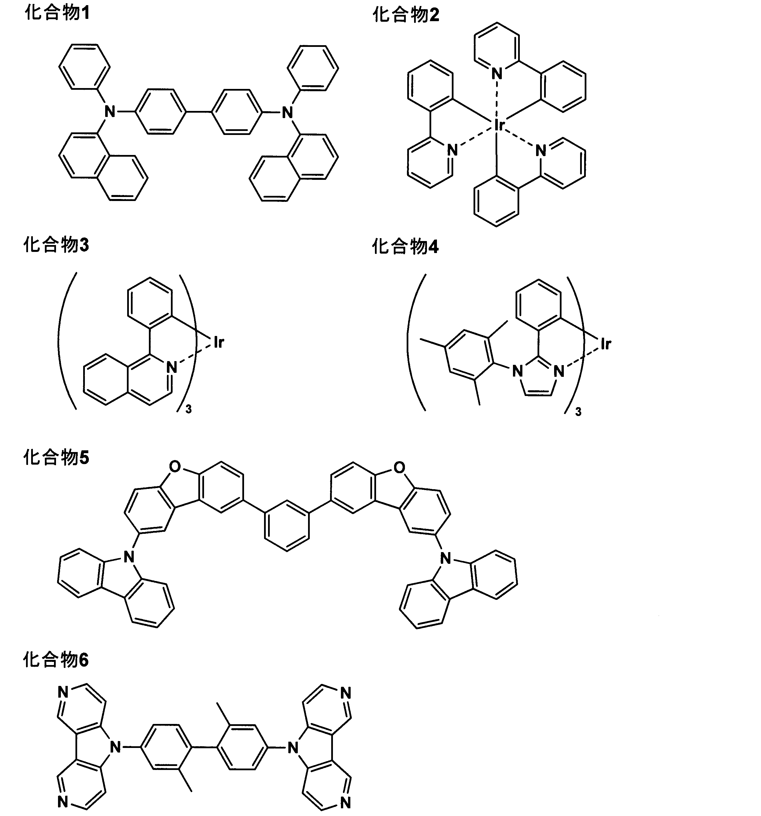
形成した電子輸送層の上に、Alを5×10⁻⁴Paの真空下にて、図4のカソード電極7の領域(1.0×1.4cm)に蒸着し、厚さ100nmのカソード電極を形成し、有機EL素子101~133及び201~205を作製した。
なお、得られた各有機EL素子は、蒸着後も大気下には出さずに窒素下で以降の評価を行った。
(短絡特性)
KEITHLEY製ソースメジャーユニット2400型を用いて、4V直流電圧を印加して正方向の電流値を求め、引き続いて-4Vの電圧を印加して逆方向の電流値を求め、(正方向の電流値)/(逆方向の電流値)が100以上であることを○とした。この場合短絡(リーク)がないとみなすことができる。
KEITHLEY製ソースメジャーユニット2400型を用いて、4V直流電圧を印加して正方向の電流値を求め、引き続いて-4Vの電圧を印加して逆方向の電流値を求め、(正方向の電流値)/(逆方向の電流値)が100以上であることを○とした。この場合短絡(リーク)がないとみなすことができる。
上記値が2以下、あるいは、素子が発光しない場合は×とした。
(駆動電圧)
KEITHLEY製ソースメジャーユニット2400型を用いて、直流電圧を印加し、3mAの電流を素子に流すのに必要な電圧を求め駆動電圧とし、以下の指標で評価した。
KEITHLEY製ソースメジャーユニット2400型を用いて、直流電圧を印加し、3mAの電流を素子に流すのに必要な電圧を求め駆動電圧とし、以下の指標で評価した。
△以上が好ましく、○△以上がより好ましい。
○ ;比較例202に対して +0.2V未満
○△;比較例202に対して +0.2V以上 +0.5V未満
△ ;比較例202に対して +0.5V以上 +0.8V未満
△×;比較例202に対して +0.8V以上 +1.2V未満
× ;比較例202に対して +1.2V以上
なお、比較例201は素子が発光せず、評価外とした。
○ ;比較例202に対して +0.2V未満
○△;比較例202に対して +0.2V以上 +0.5V未満
△ ;比較例202に対して +0.5V以上 +0.8V未満
△×;比較例202に対して +0.8V以上 +1.2V未満
× ;比較例202に対して +1.2V以上
なお、比較例201は素子が発光せず、評価外とした。
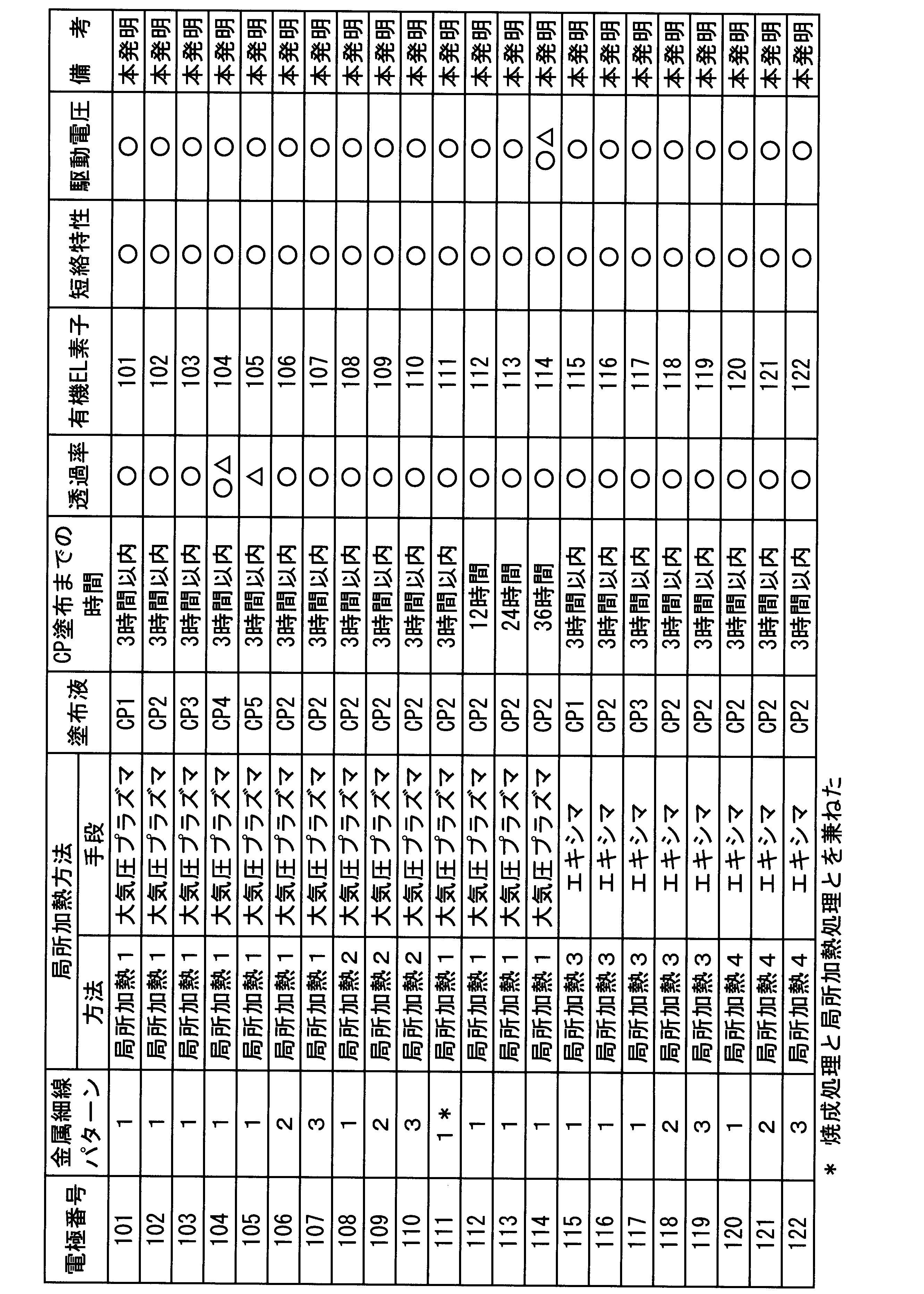

本発明の有機電子デバイス用面状電極の製造方法は高い透明性を維持しつつ、また、駆動電圧が低く、対向電極とのリークのない有機電子デバイスを与える電極を、低コストで製造することができ、有機電子デバイス用面状電極に好適に使用できる。
1、4 取り出し電極
2 金属細線パターン
3 ブランク部
5、6 導電性ポリマー含有層
7 カソード電極
10 有機電子デバイス用面状電極
2 金属細線パターン
3 ブランク部
5、6 導電性ポリマー含有層
7 カソード電極
10 有機電子デバイス用面状電極
Claims (6)
- 基材上に、金属ナノ粒子より形成された導電性の金属細線パターンと、該金属細線パターン上に少なくとも、π共役系導電性高分子とポリ陰イオンとを含んで成る導電性ポリマーと、下記一般式(I)で表される構造単位を含む水溶性バインダー樹脂とから形成された導電性ポリマー含有層とを有する有機電子デバイス用面状電極の製造方法において、該金属細線パターンに局所加熱処理を施した後に前記導電性ポリマー含有層を形成することを特徴とする有機電子デバイス用面状電極の製造方法。

- 前記局所加熱処理により前記金属細線パターンと基材が20℃以上の温度差が生じるようにすることを特徴とする請求項1に記載の有機電子デバイス用面状電極の製造方法。
- 前記局所加熱処理が、プラズマ処理、誘電加熱処理、エキシマ光照射処理、又はマイクロ波処理であることを特徴とする請求項1又は2に記載の有機電子デバイス用面状電極の製造方法。
- 前記局所加熱処理後24時間以内に導電性ポリマー含有層を形成することを特徴とする請求項1~3のいずれか1項に記載の有機電子デバイス用面状電極の製造方法。
- 前記導電性ポリマー含有層が前記一般式(I)で表される構造単位を含む水溶性バインダー樹脂を50質量%以上含有することを特徴とする請求項1~4のいずれか1項に記載の有機電子デバイス用面状電極の製造方法。
- 前記基材が二軸延伸ポリエステルであることを特徴とする請求項1~5のいずれか1項に記載の有機電子デバイス用面状電極の製造方法。
Priority Applications (1)
| Application Number | Priority Date | Filing Date | Title |
|---|---|---|---|
| JP2013504715A JP5835316B2 (ja) | 2011-03-14 | 2012-03-12 | 有機電子デバイス用面状電極の製造方法 |
Applications Claiming Priority (2)
| Application Number | Priority Date | Filing Date | Title |
|---|---|---|---|
| JP2011055246 | 2011-03-14 | ||
| JP2011-055246 | 2011-03-14 |
Publications (1)
| Publication Number | Publication Date |
|---|---|
| WO2012124647A1 true WO2012124647A1 (ja) | 2012-09-20 |
Family
ID=46830718
Family Applications (1)
| Application Number | Title | Priority Date | Filing Date |
|---|---|---|---|
| PCT/JP2012/056225 Ceased WO2012124647A1 (ja) | 2011-03-14 | 2012-03-12 | 有機電子デバイス用面状電極の製造方法 |
Country Status (2)
| Country | Link |
|---|---|
| JP (1) | JP5835316B2 (ja) |
| WO (1) | WO2012124647A1 (ja) |
Cited By (3)
| Publication number | Priority date | Publication date | Assignee | Title |
|---|---|---|---|---|
| FR2996359A1 (fr) * | 2012-10-03 | 2014-04-04 | Hutchinson | Electrode transparente conductrice et procede de fabrication associe |
| US9384907B2 (en) | 2011-07-01 | 2016-07-05 | Hutchinson | Current-conducting electrode and corresponding manufacturing process |
| WO2018235594A1 (ja) * | 2017-06-22 | 2018-12-27 | 住友化学株式会社 | 透明電極の製造方法及び電子デバイスの製造方法 |
Citations (6)
| Publication number | Priority date | Publication date | Assignee | Title |
|---|---|---|---|---|
| JP2008133322A (ja) * | 2006-11-27 | 2008-06-12 | Shin Etsu Polymer Co Ltd | 導電性高分子塗料及び導電性塗膜 |
| JP2008522369A (ja) * | 2004-11-24 | 2008-06-26 | ノバセントリックス コーポレイション | ナノ材料組成物の電気的使用、めっき的使用および触媒的使用 |
| JP2008243547A (ja) * | 2007-02-28 | 2008-10-09 | Mitsuboshi Belting Ltd | 透明電極及びその製造方法 |
| JP2010244747A (ja) * | 2009-04-02 | 2010-10-28 | Konica Minolta Holdings Inc | 透明電極、透明電極の製造方法、および有機エレクトロルミネッセンス素子 |
| WO2011148931A1 (ja) * | 2010-05-28 | 2011-12-01 | コニカミノルタホールディングス株式会社 | 有機電子デバイス用電極 |
| JP2012009240A (ja) * | 2010-06-24 | 2012-01-12 | Konica Minolta Holdings Inc | 透明電極とその製造方法、及び透明電極を用いた有機電子素子 |
-
2012
- 2012-03-12 WO PCT/JP2012/056225 patent/WO2012124647A1/ja not_active Ceased
- 2012-03-12 JP JP2013504715A patent/JP5835316B2/ja not_active Expired - Fee Related
Patent Citations (6)
| Publication number | Priority date | Publication date | Assignee | Title |
|---|---|---|---|---|
| JP2008522369A (ja) * | 2004-11-24 | 2008-06-26 | ノバセントリックス コーポレイション | ナノ材料組成物の電気的使用、めっき的使用および触媒的使用 |
| JP2008133322A (ja) * | 2006-11-27 | 2008-06-12 | Shin Etsu Polymer Co Ltd | 導電性高分子塗料及び導電性塗膜 |
| JP2008243547A (ja) * | 2007-02-28 | 2008-10-09 | Mitsuboshi Belting Ltd | 透明電極及びその製造方法 |
| JP2010244747A (ja) * | 2009-04-02 | 2010-10-28 | Konica Minolta Holdings Inc | 透明電極、透明電極の製造方法、および有機エレクトロルミネッセンス素子 |
| WO2011148931A1 (ja) * | 2010-05-28 | 2011-12-01 | コニカミノルタホールディングス株式会社 | 有機電子デバイス用電極 |
| JP2012009240A (ja) * | 2010-06-24 | 2012-01-12 | Konica Minolta Holdings Inc | 透明電極とその製造方法、及び透明電極を用いた有機電子素子 |
Cited By (9)
| Publication number | Priority date | Publication date | Assignee | Title |
|---|---|---|---|---|
| US9384907B2 (en) | 2011-07-01 | 2016-07-05 | Hutchinson | Current-conducting electrode and corresponding manufacturing process |
| FR2996359A1 (fr) * | 2012-10-03 | 2014-04-04 | Hutchinson | Electrode transparente conductrice et procede de fabrication associe |
| WO2014053572A3 (fr) * | 2012-10-03 | 2014-07-24 | Hutchinson | Electrode transparente conductrice et procede de fabrication associe |
| CN104813499A (zh) * | 2012-10-03 | 2015-07-29 | 哈钦森公司 | 导电透明电极以及相关制造工艺 |
| US20150262730A1 (en) * | 2012-10-03 | 2015-09-17 | Hutchinson | Transparent conductive electrode and associated production method |
| US9905332B2 (en) | 2012-10-03 | 2018-02-27 | Hutchinson | Transparent conductive electrode and associated production method |
| CN104813499B (zh) * | 2012-10-03 | 2018-09-11 | 哈钦森公司 | 导电透明电极以及相关制造工艺 |
| WO2018235594A1 (ja) * | 2017-06-22 | 2018-12-27 | 住友化学株式会社 | 透明電極の製造方法及び電子デバイスの製造方法 |
| JP2019008942A (ja) * | 2017-06-22 | 2019-01-17 | 住友化学株式会社 | 透明電極の製造方法及び電子デバイスの製造方法 |
Also Published As
| Publication number | Publication date |
|---|---|
| JPWO2012124647A1 (ja) | 2014-07-24 |
| JP5835316B2 (ja) | 2015-12-24 |
Similar Documents
| Publication | Publication Date | Title |
|---|---|---|
| JP5741581B2 (ja) | 透明導電膜、および有機エレクトロルミネッセンス素子 | |
| WO2017056797A1 (ja) | 透明有機エレクトロルミネッセンス素子 | |
| JP6319090B2 (ja) | 透明電極の製造方法 | |
| JP5915056B2 (ja) | 透明電極の製造方法および有機電子デバイスの製造方法 | |
| JP2012009240A (ja) | 透明電極とその製造方法、及び透明電極を用いた有機電子素子 | |
| WO2014034920A1 (ja) | 透明電極およびその製造方法ならびに有機電子デバイス | |
| JP5835316B2 (ja) | 有機電子デバイス用面状電極の製造方法 | |
| JP6036818B2 (ja) | 導電性基板の製造方法、導電性基板および有機電子素子 | |
| WO2017056814A1 (ja) | 透明有機エレクトロルミネッセンス素子及びその製造方法 | |
| JP5983173B2 (ja) | 透明電極の製造方法および有機電子素子の製造方法 | |
| WO2016143201A1 (ja) | 透明電極とその製造方法及び有機エレクトロルミネッセンス素子 | |
| JP2014104409A (ja) | 透明電極の製造方法 | |
| JP5849834B2 (ja) | 透明電極、透明電極の製造方法、及び該透明電極を用いた有機電子素子 | |
| JP2013004335A (ja) | 透明電極及び有機エレクトロルミネッセンス素子 | |
| JP5750908B2 (ja) | 透明導電膜の製造方法、透明導電膜および有機エレクトロルミネッセンス素子 | |
| WO2015050081A1 (ja) | 導電性基板、その製造方法及び当該導電性基板が備えられている有機電子デバイス | |
| JP2016110769A (ja) | 透明電極の製造方法、透明電極、透明電極の製造装置、電子機器 | |
| JP5741366B2 (ja) | 透明電極の製造方法 | |
| JP5691472B2 (ja) | 透明電極の製造方法及び有機エレクトロルミネッセンス素子の製造方法 | |
| JP6032271B2 (ja) | 透明電極の製造方法および有機電子素子の製造方法 | |
| JP5609797B2 (ja) | 透明導電膜、その形成方法および有機エレクトロルミネッセンス素子 | |
| JP2012243492A (ja) | 透明電極の製造方法および有機電子デバイス | |
| JP5617539B2 (ja) | 透明導電膜基板および有機エレクトロルミネッセンス素子 | |
| JP2012069381A (ja) | 透明導電膜、および有機エレクトロルミネッセンス素子 | |
| JP2012160391A (ja) | 透明導電膜、および有機エレクトロルミネッセンス素子 |
Legal Events
| Date | Code | Title | Description |
|---|---|---|---|
| 121 | Ep: the epo has been informed by wipo that ep was designated in this application |
Ref document number: 12757883 Country of ref document: EP Kind code of ref document: A1 |
|
| ENP | Entry into the national phase |
Ref document number: 2013504715 Country of ref document: JP Kind code of ref document: A |
|
| NENP | Non-entry into the national phase |
Ref country code: DE |
|
| 122 | Ep: pct application non-entry in european phase |
Ref document number: 12757883 Country of ref document: EP Kind code of ref document: A1 |