WO2012124561A1 - Electronic part - Google Patents
Electronic part Download PDFInfo
- Publication number
- WO2012124561A1 WO2012124561A1 PCT/JP2012/055786 JP2012055786W WO2012124561A1 WO 2012124561 A1 WO2012124561 A1 WO 2012124561A1 JP 2012055786 W JP2012055786 W JP 2012055786W WO 2012124561 A1 WO2012124561 A1 WO 2012124561A1
- Authority
- WO
- WIPO (PCT)
- Prior art keywords
- conductor
- conductors
- main surface
- outermost
- electronic component
- Prior art date
Links
- 239000004020 conductor Substances 0.000 claims abstract description 274
- 230000002093 peripheral effect Effects 0.000 claims description 7
- 229910010293 ceramic material Inorganic materials 0.000 claims description 4
- 238000009751 slip forming Methods 0.000 claims description 4
- 238000010030 laminating Methods 0.000 abstract description 4
- 238000009413 insulation Methods 0.000 abstract 5
- 239000010410 layer Substances 0.000 description 57
- 239000000919 ceramic Substances 0.000 description 7
- 239000011247 coating layer Substances 0.000 description 6
- 230000000052 comparative effect Effects 0.000 description 5
- 230000004048 modification Effects 0.000 description 5
- 238000012986 modification Methods 0.000 description 5
- 238000010304 firing Methods 0.000 description 2
- 238000000034 method Methods 0.000 description 2
- 230000000149 penetrating effect Effects 0.000 description 2
- 238000010586 diagram Methods 0.000 description 1
- 238000003475 lamination Methods 0.000 description 1
- 239000000463 material Substances 0.000 description 1
- 239000011347 resin Substances 0.000 description 1
- 229920005989 resin Polymers 0.000 description 1
- 238000007650 screen-printing Methods 0.000 description 1
- 239000000758 substrate Substances 0.000 description 1
Images


Classifications
-
- H—ELECTRICITY
- H01—ELECTRIC ELEMENTS
- H01F—MAGNETS; INDUCTANCES; TRANSFORMERS; SELECTION OF MATERIALS FOR THEIR MAGNETIC PROPERTIES
- H01F17/00—Fixed inductances of the signal type
- H01F17/0006—Printed inductances
- H01F17/0013—Printed inductances with stacked layers
-
- H—ELECTRICITY
- H01—ELECTRIC ELEMENTS
- H01G—CAPACITORS; CAPACITORS, RECTIFIERS, DETECTORS, SWITCHING DEVICES OR LIGHT-SENSITIVE DEVICES, OF THE ELECTROLYTIC TYPE
- H01G4/00—Fixed capacitors; Processes of their manufacture
- H01G4/40—Structural combinations of fixed capacitors with other electric elements, the structure mainly consisting of a capacitor, e.g. RC combinations
Definitions
- the present invention relates to an electronic component, and more particularly to an electronic component including a main body on which an insulating layer is laminated.
- an electronic component comprising a main body with an insulating layer laminated, a side conductor formed on a side surface of the main body, and a main surface conductor formed on the main surface of the main body, and the side conductor and the main surface conductor are connected. ing.
- the side conductor 15A is formed on the side surface of the main body 16 on which the insulating layers are laminated, and the main surface conductors 13a to 13g are formed on the main surface of the main body 16.
- Side conductor 15A and main surface conductors 13a to 13g are spirally connected to form spiral coil L.
- a cover layer 17 is formed on the main body 16, and the side conductor 15A and the main surface conductors 13a to 13g are covered with the cover layer 17 so as not to be exposed to the outside (see, for example, Patent Document 1).
- the coating layer needs to be formed by an appropriate method by selecting a material in consideration of the influence on the adhesion and the characteristics of the electronic component. For this reason, the coating layer cannot be easily formed, and a process for forming the coating layer needs to be added, resulting in an increase in cost.
- the present invention is intended to provide an electronic component that can improve the reliability of electrical connection between a side conductor and a main conductor without forming a coating layer.
- the present invention provides an electronic component configured as follows.
- the electronic component includes: (a) a main body including a plurality of insulating layers stacked on each other; (b) a main surface conductor formed on the main surface of the main body on at least one side in the stacking direction in which the insulating layers are stacked; (C) side conductors that pass through the insulating layers adjacent to each other, are exposed at the outer peripheral end surface of the insulating layer, and are continuously formed so as to reach the insulating layer on which the main surface conductor is formed; ) The outermost layer that penetrates through the insulating layer on which the main surface conductor is formed and at least a part of the outermost conductor is disposed on the inner side of the main body than the side conductor when viewed from the stacking direction in which the insulating layer is stacked.
- the main surface conductor and the side surface conductor are electrically connected via the outermost conductor.
- the main surface conductor and the outermost conductor include portions that are connected to each other inside the main body rather than the side conductors when viewed from the stacking direction. Compared to the case where the conductors are connected to each other only in the region where the side conductors overlap, they are connected more reliably.
- the main surface conductor and the outermost conductor are connected by providing the portion where the main surface conductor and the outermost conductor are connected at a position away from the corner where the side surface of the main body and the main surface intersect. Can be made difficult to be disconnected. Thereby, the reliability of the electrical connection between the side conductor and the main conductor is improved.
- all of the outermost conductors are arranged inside the main body rather than the side conductors when viewed from the lamination direction of the insulating layer.
- a wiring conductor that electrically connects the outermost conductor and the side conductor is formed between the insulating layer on which the main surface conductor is formed and the insulating layer adjacent to the insulating layer.
- the main surface conductor and the side surface conductor are electrically connected via the outermost conductor and the wiring conductor.
- the main surface conductor is connected to the outermost conductor formed away from the vicinity of the corner of the main body. Compared with the case where the main surface conductor is connected in the vicinity of the corner of the main body, it is possible to prevent the connecting portion with the outermost conductor from being rubbed and worn or peeled off from the main body. Therefore, the reliability of electrical connection between the main surface conductor and the side surface conductor is further improved.
- the outermost conductor is exposed on an outer peripheral end face of the insulating layer on which the main surface conductor is formed.
- the outermost conductor overlaps the side conductor and protrudes outside the side conductor when viewed from the stacking direction.
- the outermost conductor and the side conductor can be connected without using the wiring conductor that connects the outermost conductor and the side conductor, and the configuration can be simplified.
- the main surface conductor and the outermost conductor when viewed from the stacking direction, have a shape obtained by dividing circles having different diameters arranged concentrically.
- an electronic component can be manufactured by forming concentric and different diameter through holes in the insulating layer through which the outermost conductor penetrates and the insulating layer through which the side conductor penetrates, thereby simplifying the configuration. .
- the insulating layer through which the side conductor and the outermost conductor penetrate includes a magnetic ceramic material.
- an electronic component including an inductor element can be formed.
- the electronic component is an inductor element in which a coil conductor is formed by the main surface conductor, the side surface conductor, and the outermost conductor that are electrically connected to each other.
- the reliability of electrical connection between the side conductor and the main conductor can be improved without forming a coating layer.
- Example 1 It is principal part sectional drawing of an electronic component.
- Example 1 It is the schematic which shows the external appearance of an electronic component.
- Modification It is a disassembled perspective view of an electronic component.
- Modification It is the schematic which shows the external appearance of an electronic component.
- Example 2 It is principal part sectional drawing of an electronic component.
- Example 2 It is the schematic which shows the external appearance of an electronic component.
- Comparative example It is principal part sectional drawing of an electronic component.
- Comparative example It is principal part sectional drawing of an electronic component.
- Comparative example It is principal part sectional drawing of an electronic component.
- Comparative example It is a perspective view of an electronic component.
- Conventional example
- Example 1 An electronic component 10 of Example 1 will be described with reference to FIGS. 1 and 2.
- FIG. 1 is a schematic view showing the external appearance of the electronic component 10.
- FIG. 2 is a cross-sectional view of a principal part taken along line AA in FIG.
- main surface conductors 16a and 16b are formed on the main surfaces 12a and 12b of the main body 12 on which the insulating layers 12p to 12w are laminated.
- the side conductors 14 (side surfaces) that pass through the insulating layers 12q to 12v and are exposed to the outer peripheral end surfaces of the insulating layers 12q to 12v, that is, the pair of side surfaces 12c and 12d that face each other, are adjacent to the adjacent insulating layers 12q to 12v. Only the 12c side is shown).
- the side conductors 14 are continuously formed so as to reach the insulating layers 12p and 12w where the main surface conductors 16a and 16b are formed.
- Outer conductors 14a and 14b penetrating through the insulating layers 12p and 12w are formed on the insulating layers 12p and 12w on which the main surface conductors 16a and 16b are formed.
- the outermost conductors 14a and 14b are formed so that all of the outermost conductors 14a and 14b are more than the side conductors 14 when viewed from the stacking direction of the insulating layers 12p to 12w (vertical direction in FIGS. 1 and 2). It is formed so that it may be arranged inside.
- the electronic component 10 is a module component including an LC filter, for example.
- the main surface conductors 16a and 16b, the outermost conductors 14a and 14b, the wiring conductors 15a and 15b, and the side conductors 14 are spirally connected to form an inductor element.
- the insulating layers 12p to 12w include a magnetic ceramic material.
- a connection electrode 16 s for mounting another electronic component on the electronic component 10 may be formed on a part of the main surface conductor 16 a of the one main surface 12 a of the main body 12. Moreover, you may form the external electrode not shown for mounting the electronic component 10 on a circuit board etc. by a part of main surface conductor 16b of the other main surface 12b of the main body 12. FIG.
- the side conductor 14 and the main conductors 16a and 16b are electrically connected via the wiring conductors 15a and 15b and the outermost conductors 14a and 14b.
- the main surface conductors 16a, 16b and the outermost conductors 14a, 14b are connected at positions away from corners 12m, 12n, 12i, 12j where the side surfaces 12c, 12d of the main body 12 and the main surfaces 12a, 12b intersect. .
- the electronic component 10 can be produced by, for example, laminating ceramic green sheets, dividing them, and firing them.
- a through hole in the ceramic green sheet by forming a through hole in the ceramic green sheet and filling the through hole with a conductive paste, via hole conductors that become the side conductors 14 and the outermost conductors 14a and 14b are formed. Further, a conductive paste is applied to the front or back surface of the ceramic green sheet by screen printing or the like to form in-plane conductor patterns that become the main surface conductors 16a and 16b and the wiring conductors 15a and 15b.
- ceramic green sheets are laminated and pressure-bonded to form a laminated body, and the laminated body is cut so as to divide the via-hole conductor that becomes the side conductor, and is divided into pieces.
- the individual pieces are baked, and if necessary, the surface of the portions that become the side conductors 14 and the main conductors 16a and 16b is plated.
- an electronic component including only an inductor element may be manufactured instead of the module component.
- an insulating layer may be a dielectric ceramic layer to produce a dielectric ceramic element or module component.
- FIG. 3 is a schematic view showing the external appearance of the electronic component 10k.
- FIG. 4 is an exploded perspective view of the electronic component 10k.
- main surface conductors 16g to 16j and 16u to 16w are formed on the main surfaces 12a and 12b of the main body 12 on which the insulating layers 12p to 12w are laminated, as shown in FIGS.
- the insulating layers 12p to 12w are formed using a magnetic ceramic material.
- the electronic component 10k includes main surface conductors 16g to 16j, 16u to 16w, outermost conductors 24g to 24i, 24u to 24w; 25g to 25i, 25u to 25w, wiring conductors 26g to 26i, 26u to 26w; 27g to 27i, 27u to 27w, and side conductors 14g to 14i, 14u to 14w are formed by laminating and firing insulating layers 12p to 12w in which portions are formed in advance.
- the insulating layers 12p and 12w at both ends in the stacking direction are formed by forming main surface conductors 16g to 16j and 16u to 16w on the main surfaces that become the main surfaces 12a and 12b of the main body 12.
- Outer conductors 24g-24i, 24u-24w; 25g-25i, 25u-25w penetrating the layers 12p, 12w are formed.
- Side conductors 14g to 14i and 14u to 14w are formed along the outer peripheral end surfaces of the insulating layers 12q to 12v which are arranged between the insulating layers 12p and 12w at both ends in the stacking direction and are adjacent to each other.
- the side conductors 14g to 14i; 14u to 14w are connected to each other in the stacking direction and reach the insulating layers 12p and 12w at both ends in the stacking direction.
- the side conductors 14 g to 14 i are exposed on one side 12 c of the main body 12.
- the side conductors 14u to 14w are also exposed on the other side surface 12d of the main body 12 in the same manner.
- the insulating layers 12q and 12v adjacent to the insulating layers 12p and 12w at both ends in the stacking direction have wiring conductors 26g to 26i, 26u to 26w; 27g on the main surface facing the insulating layers 12p and 12w. To 27i and 27u to 27w are formed.
- the wiring conductors 26g-26i, 26u-26w; 27g-27i, 27u-27w are outermost conductors 24g-24i, 24u-24w; 25g-25i, 25u-25w formed on the insulating layers 12p, 12w at both ends in the stacking direction. Connected to.
- Main surface conductors 16g-16j, 16p-16r, outermost conductors 24g-24i, 24u-24w; 25g-25i, 25u-25w and side conductors 14g-14i, 14u-14w are electrically connected to each other. Forming a coil conductor.
- the main surface conductors 16g to 16j, 16u to 16w and the outermost conductors 24g to 24i, 24u to 24w; 25g to 25i, 25u to 25w are corners where the side surfaces 12c and 12d of the main body 12 intersect with the main surfaces 12a and 12b. They are connected at positions away from 12m, 12n, 12i, and 12j. Accordingly, it is possible to suppress disconnection of the connection between the main surface conductors 16g to 16j and 16u to 16w and the outermost conductors 24g to 24i and 24u to 24w; 25g to 25i and 25u to 25w.
- the reliability of the electrical connection between ⁇ 14i and 14u to 14w and the main surface conductors 16g to 16j and 16u to 16w is improved.
- the electronic component 10k can be mounted on the mounting substrate by using the wide portions 16p and 16q of the main surface conductors 16g and 16j formed on the one main surface 10a of the electronic component 10k as connection electrodes.
- end electrodes 12e and 12f (see FIG. 3) of the main body 12 and external electrodes covering the vicinity thereof are formed on both ends of the main body 12, and the external electrodes are formed on both ends of the coil conductor.
- the principal surface conductors 16g and 16j may be connected.
- Example 2 An electronic component 10a of Example 1 will be described with reference to FIGS.
- FIG. 5 is a schematic view showing the appearance of the electronic component 10a.
- FIG. 6 is a cross-sectional view of a principal part taken along line AA in FIG.
- the electronic component 10a is configured in substantially the same manner as the electronic component 10 of the first embodiment.
- symbol is used for the component similar to Example 1, and it demonstrates centering around difference.
- the main surface conductor 16c is formed only on one main surface 12a of the main body 12 on which the insulating layers 12p to 12w are laminated.
- the outermost conductor 14c formed on the insulating layer 12p on which the main surface conductor 16c is formed is exposed on the outer peripheral end surface (that is, the side surface 12c of the main body 12) of the insulating layer 12p on which the main surface conductor 16c is formed, and When viewed from the stacking direction, it overlaps the side conductor 14k and protrudes outside the side conductor 14k.
- the outermost conductor 14c and the side conductor 14k have a substantially semicircular shape obtained by dividing circles having different diameters arranged concentrically, and the outer diameter of the outermost conductor 14c is the side conductor. It is larger than the outer diameter of 14k.
- the side conductor 14k is continuously formed on the insulating layers 12p to 12t between the insulating layer 12q adjacent to the insulating layer 12p on which the main surface conductor 16c is formed and the insulating layer 12t at the intermediate position in the main body 12. Yes.
- One end 14p of the side conductor 14k is connected to the outermost conductor 14c.
- the other end 14q of the side conductor 14k is connected to a wiring conductor 15c formed between the insulating layers 12t and 12u at an intermediate position in the main body 12.
- the side conductor 14k and the main conductor 16c are electrically connected via the outermost conductor 14c.
- the main surface conductor 16c and the outermost conductor 14c are connected to each other at a position inside the main body 12 relative to the side surface conductor 14k when viewed from the stacking direction.
- the main surface conductor 16c and the outermost conductor 16c are provided. It is possible to make it difficult to disconnect the connection with the outer conductor 14c. This improves the reliability of electrical connection between the side conductors 14k and the main conductor 16c.
- FIG. 7 is a schematic diagram showing the external appearance of the electronic component 10x.
- 8 and 9 are cross-sectional views of the main part taken along line AA in FIG.
- side conductors 14x are formed on all the insulating layers of the main body 12. Ends 16p and 16q of main surface conductors 16x and 16y formed on main surfaces 12a and 12b of the main body 12 are connected to both ends 14y and 14z of the side conductor 14x. That is, the end portions 16p and 16q of the main surface conductors 16x and 16y are formed so as to reach the corner portions 12m and 12n of the main body 12, and are connected to the side conductors 14x in the vicinity of the corner portions 12m and 12n of the main body 12. .
- the end portions 16p and 16q of the main surface conductors 16x and 16y are formed in the vicinity of the corner portions 12m and 12n of the main body 12.
- the vicinity of the corner portions 12m and 12n of the main body 12 is the portion that is most easily rubbed before the electronic component 10x is mounted on the circuit board. Therefore, the main body 12 is thinned or peeled off, and ends of the main surface conductors 16x and 16y.
- the parts 16p and 16q are easily disconnected as schematically shown in FIG.
- the main surface conductor and the outermost conductor are configured so as to include a portion connected to each other inside the main body rather than the side surface conductor when viewed from the stacking direction.
- the reliability of the electrical connection between the side conductor and the main conductor can be improved without forming a layer.
- the insulating layer of the main body is not limited to ceramic but may be formed of resin or the like.
Landscapes
- Engineering & Computer Science (AREA)
- Power Engineering (AREA)
- Microelectronics & Electronic Packaging (AREA)
- Manufacturing & Machinery (AREA)
- Coils Or Transformers For Communication (AREA)
Abstract
Provided is an electronic part, wherein reliability of electrical connections between side face conductors and main-face conductors can be improved without forming a cover layer. The electronic part is provided with: (a) a main body (12) comprising a plurality of insulation layers (12p-12w) laminated together; (b) main-face conductors (16a/16b) formed on at least one main face (12a/12b) at one side in the laminating direction of the main body (12); (c) side face conductors (14) that penetrate insulation layers (12q-12v), that are exposed at the outer circumference end faces of the insulation layers (12q-12v), and that are formed continuously so as to reach insulation layers (12p, 12w) on which the main-face conductors (16a, 16b) are formed; and (d) outermost conductors (14a, 14b) that penetrate the insulation layers (12p, 12w) on which the main-face conductors (16a, 16b) are formed, and at least portions of which are arranged more to the inner side of the main body (12) than the side face conductors (14), when viewed from the laminating direction. The main-face conductors (16a, 16b) and the side face conductors (14) are electrically connected with the outermost conductors (14a, 14b) interposed therebetween.
Description
本発明は、電子部品に関し、詳しくは、絶縁層が積層された本体を備える電子部品に関する。
The present invention relates to an electronic component, and more particularly to an electronic component including a main body on which an insulating layer is laminated.
絶縁層が積層された本体、本体の側面に形成された側面導体と、本体の主面に形成された主面導体とを備え、側面導体と主面導体とが接続された電子部品が提供されている。
Provided is an electronic component comprising a main body with an insulating layer laminated, a side conductor formed on a side surface of the main body, and a main surface conductor formed on the main surface of the main body, and the side conductor and the main surface conductor are connected. ing.
例えば、図10の斜視図に示す積層インダクタ11は、絶縁層が積層された本体16の側面に側面導体15Aが形成され、本体16の主面に主面導体13a~13gが形成されている。側面導体15Aと主面導体13a~13gとは螺旋状に接続されて螺旋状コイルLを形成する。本体16には被覆層17が形成され、側面導体15Aと主面導体13a~13gは、被覆層17で覆われ、外部に露出しないようになっている(例えば、特許文献1参照)。
For example, in the multilayer inductor 11 shown in the perspective view of FIG. 10, the side conductor 15A is formed on the side surface of the main body 16 on which the insulating layers are laminated, and the main surface conductors 13a to 13g are formed on the main surface of the main body 16. Side conductor 15A and main surface conductors 13a to 13g are spirally connected to form spiral coil L. A cover layer 17 is formed on the main body 16, and the side conductor 15A and the main surface conductors 13a to 13g are covered with the cover layer 17 so as not to be exposed to the outside (see, for example, Patent Document 1).
側面導体と主面導体とを被覆層で覆うと、側面導体と主面導体との接続の信頼性が向上する。
覆 う Covering the side conductor and the main surface conductor with a coating layer improves the reliability of the connection between the side conductor and the main surface conductor.
しかし、被覆層は、密着性や電子部品の特性に与える影響などを考慮して材料を選択し、適切な方法で形成する必要がある。そのため、被覆層は容易には形成できない上、被覆層を形成する工程を追加する必要があり、コストの増大を招く。
However, the coating layer needs to be formed by an appropriate method by selecting a material in consideration of the influence on the adhesion and the characteristics of the electronic component. For this reason, the coating layer cannot be easily formed, and a process for forming the coating layer needs to be added, resulting in an increase in cost.
本発明は、かかる実情に鑑み、被覆層を形成することなく、側面導体と主面導体との電気的接続の信頼性を向上することができる電子部品を提供しようとするものである。
In view of such circumstances, the present invention is intended to provide an electronic component that can improve the reliability of electrical connection between a side conductor and a main conductor without forming a coating layer.
本発明は、上記課題を解決するために、以下のように構成した電子部品を提供する。
In order to solve the above problems, the present invention provides an electronic component configured as follows.
電子部品は、(a)互いに積層された複数の絶縁層を含む本体と、(b)前記絶縁層が積層された積層方向の少なくとも片側の前記本体の主面に形成された主面導体と、(c)互いに隣接する前記絶縁層を貫通し、前記絶縁層の外周端面に露出し、前記主面導体が形成された前記絶縁層に達するように連続して形成された側面導体と、(d)前記主面導体が形成された前記絶縁層を貫通し、少なくとも一部が、前記絶縁層が積層された積層方向から見たときに前記側面導体よりも前記本体の内側に配置された最外導体とを備える。前記主面導体と前記側面導体とが、前記最外導体を介して電気的に接続されている。
The electronic component includes: (a) a main body including a plurality of insulating layers stacked on each other; (b) a main surface conductor formed on the main surface of the main body on at least one side in the stacking direction in which the insulating layers are stacked; (C) side conductors that pass through the insulating layers adjacent to each other, are exposed at the outer peripheral end surface of the insulating layer, and are continuously formed so as to reach the insulating layer on which the main surface conductor is formed; ) The outermost layer that penetrates through the insulating layer on which the main surface conductor is formed and at least a part of the outermost conductor is disposed on the inner side of the main body than the side conductor when viewed from the stacking direction in which the insulating layer is stacked. A conductor. The main surface conductor and the side surface conductor are electrically connected via the outermost conductor.
上記構成において、主面導体と最外導体とは、積層方向から見たときに側面導体よりも本体の内側において互いに接続される部分を含むため、積層方向から見たときに主面導体と側面導体とが側面導体とが重なる領域のみで互いに接続される場合に比べ、より確実に互いに接続される。
In the above configuration, the main surface conductor and the outermost conductor include portions that are connected to each other inside the main body rather than the side conductors when viewed from the stacking direction. Compared to the case where the conductors are connected to each other only in the region where the side conductors overlap, they are connected more reliably.
上記構成によれば、本体の側面と主面が交わる角部から離れた位置に、主面導体と最外導体とが接続される部分を設けることにより、主面導体と最外導体との接続を断線されにくくすることができる。これによって、側面導体と主面導体との電気的接続の信頼性が向上する。
According to the above configuration, the main surface conductor and the outermost conductor are connected by providing the portion where the main surface conductor and the outermost conductor are connected at a position away from the corner where the side surface of the main body and the main surface intersect. Can be made difficult to be disconnected. Thereby, the reliability of the electrical connection between the side conductor and the main conductor is improved.
好ましい一態様において、前記最外導体の全部が、前記絶縁層の積層方向から見たときに前記側面導体よりも前記本体の内側に配置されている。前記主面導体が形成された前記絶縁層と、該絶縁層に隣接する前記絶縁層との間に、前記最外導体と前記側面導体とを電気的に接続する配線導体が形成されている。
In a preferred aspect, all of the outermost conductors are arranged inside the main body rather than the side conductors when viewed from the lamination direction of the insulating layer. A wiring conductor that electrically connects the outermost conductor and the side conductor is formed between the insulating layer on which the main surface conductor is formed and the insulating layer adjacent to the insulating layer.
この場合、主面導体と側面導体とは、最外導体及び配線導体を介して電気的に接続される。主面導体は、本体の角部近傍から離れて形成された最外導体と接続される。主面導体は、本体の角部近傍で接続される場合に比べ、最外導体との接続部分が擦れて摩耗したり、本体から剥がれたりすることを抑制することができる。そのため、主面導体と側面導体との電気的接続の信頼性がより向上する。
In this case, the main surface conductor and the side surface conductor are electrically connected via the outermost conductor and the wiring conductor. The main surface conductor is connected to the outermost conductor formed away from the vicinity of the corner of the main body. Compared with the case where the main surface conductor is connected in the vicinity of the corner of the main body, it is possible to prevent the connecting portion with the outermost conductor from being rubbed and worn or peeled off from the main body. Therefore, the reliability of electrical connection between the main surface conductor and the side surface conductor is further improved.
好ましい他の態様において、前記最外導体は、前記主面導体が形成された前記絶縁層の外周端面に露出する。前記最外導体は、前記積層方向から見たとき、前記側面導体に重なり、かつ前記側面導体の外側にはみ出ている。
In another preferable aspect, the outermost conductor is exposed on an outer peripheral end face of the insulating layer on which the main surface conductor is formed. The outermost conductor overlaps the side conductor and protrudes outside the side conductor when viewed from the stacking direction.
この場合、最外導体と側面導体とを接続する配線導体を介することなく、最外導体と側面導体とを接続でき、構成を簡単にすることができる。
In this case, the outermost conductor and the side conductor can be connected without using the wiring conductor that connects the outermost conductor and the side conductor, and the configuration can be simplified.
上記した他の態様において、好ましくは、前記積層方向から見たとき、前記主面導体と前記最外導体とは、同心に配置された径の異なる円を分割した形状を有する。
In the other aspect described above, preferably, when viewed from the stacking direction, the main surface conductor and the outermost conductor have a shape obtained by dividing circles having different diameters arranged concentrically.
この場合、同心かつ径が異なる貫通孔を、最外導体が貫通する絶縁層と、側面導体が貫通する絶縁層とにそれぞれ形成することにより電子部品を製造することができ、構成が簡単になる。
In this case, an electronic component can be manufactured by forming concentric and different diameter through holes in the insulating layer through which the outermost conductor penetrates and the insulating layer through which the side conductor penetrates, thereby simplifying the configuration. .
好ましくは、前記側面導体及び前記最外導体が貫通する前記絶縁層が、磁性体セラミック材料を含む。
Preferably, the insulating layer through which the side conductor and the outermost conductor penetrate includes a magnetic ceramic material.
この場合、インダクタ素子を含む電子部品を形成することができる。
In this case, an electronic component including an inductor element can be formed.
好ましい一態様において、電子部品は、互いに電気的に接続された前記主面導体と前記側面導体と前記最外導体とによりコイル導体が形成されたインダクタ素子である。
In a preferred aspect, the electronic component is an inductor element in which a coil conductor is formed by the main surface conductor, the side surface conductor, and the outermost conductor that are electrically connected to each other.
本発明によれば、被覆層を形成することなく、側面導体と主面導体との電気的接続の信頼性を向上することができる。
According to the present invention, the reliability of electrical connection between the side conductor and the main conductor can be improved without forming a coating layer.
以下、本発明の実施の形態について、図1~図9を参照しながら説明する。
Hereinafter, embodiments of the present invention will be described with reference to FIGS.
<実施例1> 実施例1の電子部品10について、図1及び図2を参照しながら説明する。
Example 1 An electronic component 10 of Example 1 will be described with reference to FIGS. 1 and 2.
図1は、電子部品10の外観を示す概略図である。図2は、図1の線A-Aに沿って切断した要部断面図である。
FIG. 1 is a schematic view showing the external appearance of the electronic component 10. FIG. 2 is a cross-sectional view of a principal part taken along line AA in FIG.
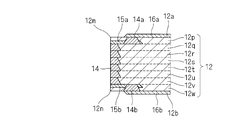
図1及び図2に示すように、電子部品10は、絶縁層12p~12wが積層された本体12の主面12a,12bに、主面導体16a,16bが形成されている。
As shown in FIGS. 1 and 2, in the electronic component 10, main surface conductors 16a and 16b are formed on the main surfaces 12a and 12b of the main body 12 on which the insulating layers 12p to 12w are laminated.
互いに隣接する絶縁層12q~12vには、絶縁層12q~12vを貫通し、絶縁層12q~12vの外周端面、すなわち本体12の互いに対向する一対の側面12c,12dに露出する側面導体14(側面12c側のみ図示)が形成されている。側面導体14は、主面導体16a,16bが形成された絶縁層12p,12wに達するように連続して形成されている。
The side conductors 14 (side surfaces) that pass through the insulating layers 12q to 12v and are exposed to the outer peripheral end surfaces of the insulating layers 12q to 12v, that is, the pair of side surfaces 12c and 12d that face each other, are adjacent to the adjacent insulating layers 12q to 12v. Only the 12c side is shown). The side conductors 14 are continuously formed so as to reach the insulating layers 12p and 12w where the main surface conductors 16a and 16b are formed.
主面導体16a,16bが形成された絶縁層12p,12wには、絶縁層12p,12wを貫通する最外導体14a,14bが形成されている。最外導体14a,14bは、絶縁層12p~12wの積層方向(図1及び図2において、上下方向)から見たときに、最外導体14a,14bの全部が、側面導体14よりも本体12の内側に配置されるように、形成されている。
Outer conductors 14a and 14b penetrating through the insulating layers 12p and 12w are formed on the insulating layers 12p and 12w on which the main surface conductors 16a and 16b are formed. The outermost conductors 14a and 14b are formed so that all of the outermost conductors 14a and 14b are more than the side conductors 14 when viewed from the stacking direction of the insulating layers 12p to 12w (vertical direction in FIGS. 1 and 2). It is formed so that it may be arranged inside.
主面導体16a,16bが形成された絶縁層12p,12wの主面のうち、主面導体16a,16bが形成された主面12a,12bとは反対側の主面に沿って、最外導体14a,14bと側面導体14とを電気的に接続する配線導体15a,15bが形成されている。
Out of the main surfaces of the insulating layers 12p and 12w on which the main surface conductors 16a and 16b are formed, the outermost conductors along the main surface opposite to the main surfaces 12a and 12b on which the main surface conductors 16a and 16b are formed. Wiring conductors 15a and 15b that electrically connect 14a and 14b and the side conductors 14 are formed.
電子部品10は、例えば、LCフィルタを含むモジュール部品である。この場合、主面導体16a,16bと、最外導体14a,14bと、配線導体15a,15bと、側面導体14とを螺旋状に接続し、インダクタ素子を形成する。絶縁層12p~12wは、磁性体セラミック材料を含むようにする。
The electronic component 10 is a module component including an LC filter, for example. In this case, the main surface conductors 16a and 16b, the outermost conductors 14a and 14b, the wiring conductors 15a and 15b, and the side conductors 14 are spirally connected to form an inductor element. The insulating layers 12p to 12w include a magnetic ceramic material.
電子部品10は、本体12の一方の主面12aの主面導体16aの一部に、電子部品10に他の電子部品を搭載するための接続電極16sを形成してもよい。また、本体12の他方の主面12bの主面導体16bの一部によって、電子部品10を回路基板等に実装するための不図示の外部電極を形成してもよい。
In the electronic component 10, a connection electrode 16 s for mounting another electronic component on the electronic component 10 may be formed on a part of the main surface conductor 16 a of the one main surface 12 a of the main body 12. Moreover, you may form the external electrode not shown for mounting the electronic component 10 on a circuit board etc. by a part of main surface conductor 16b of the other main surface 12b of the main body 12. FIG.
側面導体14と主面導体16a,16bとは、配線導体15a,15b及び最外導体14a,14bを介して電気的に接続されている。主面導体16a,16bと最外導体14a,14bとは、本体12の側面12c,12dと主面12a,12bとが交わる角部12m,12n,12i,12jから離れた位置で接続されている。これによって、主面導体16a,16bと最外導体14a,14bとの接続が断線することを抑制することができるので、側面導体14と主面導体16a,16bとの電気的接続の信頼性が向上する。
The side conductor 14 and the main conductors 16a and 16b are electrically connected via the wiring conductors 15a and 15b and the outermost conductors 14a and 14b. The main surface conductors 16a, 16b and the outermost conductors 14a, 14b are connected at positions away from corners 12m, 12n, 12i, 12j where the side surfaces 12c, 12d of the main body 12 and the main surfaces 12a, 12b intersect. . As a result, it is possible to suppress disconnection of the connection between the main surface conductors 16a and 16b and the outermost conductors 14a and 14b. Therefore, the reliability of the electrical connection between the side surface conductor 14 and the main surface conductors 16a and 16b is improved. improves.
電子部品10は、例えば、セラミックグリーンシートを積層し、分割した後に焼成することによって、作製できる。
The electronic component 10 can be produced by, for example, laminating ceramic green sheets, dividing them, and firing them.
すなわち、セラミックグリーンシートに貫通孔を形成し、貫通孔に導電性ペーストを充填することにより、側面導体14や最外導体14a,14bになるビアホール導体を形成する。さらに、セラミックグリーンシートの表面又は裏面に導電性ペーストをスクリーン印刷等により塗布し、主面導体16a,16bや配線導体15a,15bになる面内導体パターンを形成する。
That is, by forming a through hole in the ceramic green sheet and filling the through hole with a conductive paste, via hole conductors that become the side conductors 14 and the outermost conductors 14a and 14b are formed. Further, a conductive paste is applied to the front or back surface of the ceramic green sheet by screen printing or the like to form in-plane conductor patterns that become the main surface conductors 16a and 16b and the wiring conductors 15a and 15b.
次いで、セラミックグリーンシートを積層、圧着して積層体を形成し、側面導体になるビアホール導体を分割するように積層体を切断して、個片に分割する。
Next, ceramic green sheets are laminated and pressure-bonded to form a laminated body, and the laminated body is cut so as to divide the via-hole conductor that becomes the side conductor, and is divided into pieces.
次いで、個片を焼成し、必要に応じて、側面導体14や主面導体16a,16bになる部分の表面にめっき処理を施す。
Next, the individual pieces are baked, and if necessary, the surface of the portions that become the side conductors 14 and the main conductors 16a and 16b is plated.
なお、実施例1の構成により、モジュール部品の代わりに、インダクタ素子のみを含む電子部品を作製してもよい。
In addition, according to the configuration of the first embodiment, an electronic component including only an inductor element may be manufactured instead of the module component.
また、実施例1の構成において絶縁層を誘電体セラミック層にすることにより、誘電体セラミックからなる素子や、モジュール部品を作製してもよい。
Also, in the configuration of the first embodiment, an insulating layer may be a dielectric ceramic layer to produce a dielectric ceramic element or module component.
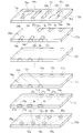
<変形例> インダクタ素子のみを含む変形例の電子部品10k、すなわち、インダクタ素子である電子部品10kについて、図3及び図4を参照しながら説明する。
<Modification> An electronic component 10k of a modification including only an inductor element, that is, an electronic component 10k that is an inductor element will be described with reference to FIGS.
図3は、電子部品10kの外観を示す概略図である。図4は、電子部品10kの分解斜視図である。
FIG. 3 is a schematic view showing the external appearance of the electronic component 10k. FIG. 4 is an exploded perspective view of the electronic component 10k.
電子部品10kは、図3及び図4に示すように、絶縁層12p~12wが積層された本体12の主面12a,12bに、主面導体16g~16j,16u~16wが形成されている。絶縁層12p~12wは、磁性体セラミック材料を用いて形成されている。
In the electronic component 10k, main surface conductors 16g to 16j and 16u to 16w are formed on the main surfaces 12a and 12b of the main body 12 on which the insulating layers 12p to 12w are laminated, as shown in FIGS. The insulating layers 12p to 12w are formed using a magnetic ceramic material.
図4に示すように、電子部品10kは、主面導体16g~16j,16u~16w、最外導体24g~24i,24u~24w;25g~25i,25u~25w、配線導体26g~26i,26u~26w;27g~27i,27u~27w、側面導体14g~14i,14u~14wになる部分が予め形成された絶縁層12p~12wを積層し、焼成することにより、作製される。
As shown in FIG. 4, the electronic component 10k includes main surface conductors 16g to 16j, 16u to 16w, outermost conductors 24g to 24i, 24u to 24w; 25g to 25i, 25u to 25w, wiring conductors 26g to 26i, 26u to 26w; 27g to 27i, 27u to 27w, and side conductors 14g to 14i, 14u to 14w are formed by laminating and firing insulating layers 12p to 12w in which portions are formed in advance.
詳しくは、積層方向(図4において上下方向)両端の絶縁層12p,12wは、本体12の主面12a,12bになる主面に、主面導体16g~16j,16u~16wが形成され、絶縁層12p,12wを貫通する最外導体24g~24i,24u~24w;25g~25i,25u~25wが形成される。
Specifically, the insulating layers 12p and 12w at both ends in the stacking direction (vertical direction in FIG. 4) are formed by forming main surface conductors 16g to 16j and 16u to 16w on the main surfaces that become the main surfaces 12a and 12b of the main body 12. Outer conductors 24g-24i, 24u-24w; 25g-25i, 25u-25w penetrating the layers 12p, 12w are formed.
積層方向両端の絶縁層12p,12wの間に配置され、互いに隣接する絶縁層12q~12vには、それぞれの外周端面に沿って側面導体14g~14i,14u~14wが形成される。側面導体14g~14i;14u~14wは積層方向に互いに接続され、積層方向両端の絶縁層12p,12wに達している。図3に示すように、側面導体14g~14iは、本体12の一方の側面12cに露出する。図3には図示していないが、側面導体14u~14wも同様に、本体12の他方の側面12dに露出する。
Side conductors 14g to 14i and 14u to 14w are formed along the outer peripheral end surfaces of the insulating layers 12q to 12v which are arranged between the insulating layers 12p and 12w at both ends in the stacking direction and are adjacent to each other. The side conductors 14g to 14i; 14u to 14w are connected to each other in the stacking direction and reach the insulating layers 12p and 12w at both ends in the stacking direction. As shown in FIG. 3, the side conductors 14 g to 14 i are exposed on one side 12 c of the main body 12. Although not shown in FIG. 3, the side conductors 14u to 14w are also exposed on the other side surface 12d of the main body 12 in the same manner.
図4に示すように、積層方向両端の絶縁層12p,12wに隣接する絶縁層12q,12vには、絶縁層12p,12wに対向する主面に、配線導体26g~26i,26u~26w;27g~27i,27u~27wが形成されている。配線導体26g~26i,26u~26w;27g~27i,27u~27wは、積層方向両端の絶縁層12p,12wに形成された最外導体24g~24i,24u~24w;25g~25i,25u~25wに接続される。
As shown in FIG. 4, the insulating layers 12q and 12v adjacent to the insulating layers 12p and 12w at both ends in the stacking direction have wiring conductors 26g to 26i, 26u to 26w; 27g on the main surface facing the insulating layers 12p and 12w. To 27i and 27u to 27w are formed. The wiring conductors 26g-26i, 26u-26w; 27g-27i, 27u-27w are outermost conductors 24g-24i, 24u-24w; 25g-25i, 25u-25w formed on the insulating layers 12p, 12w at both ends in the stacking direction. Connected to.
主面導体16g~16j,16p~16rと、最外導体24g~24i,24u~24w;25g~25i,25u~25wと、側面導体14g~14i,14u~14wとは、互いに電気的に接続され、コイル導体を形成する。
Main surface conductors 16g-16j, 16p-16r, outermost conductors 24g-24i, 24u-24w; 25g-25i, 25u-25w and side conductors 14g-14i, 14u-14w are electrically connected to each other. Forming a coil conductor.
すなわち、図3及び図4に示すように、本体12の一方の主面12aにおいて最も左側の主面導体16gから順に、最外導体24g、配線導体26g、側面導体14g、配線導体27g、最外導体25g、主面導体16u、最外導体25u、配線導体27u、側面導体14u、配線導体26u、最外導体24u、主面導体16h、最外導体24h、配線導体26h、側面導体14h、配線導体27h、最外導体25h、主面導体16v、最外導体25v、配線導体27v、側面導体14v、配線導体26v、最外導体24v、主面導体16i、最外導体24i、配線導体26i、側面導体14i、配線導体27i、最外導体25i、主面導体16w、最外導体25w、配線導体27w、側面導体14w、配線導体26w、最外導体24wを経て、本体12の一方の主面12aにおいて最も右側の主面導体16jまで、螺旋状に接続され、コイル導体が形成される。
That is, as shown in FIG. 3 and FIG. 4, the outermost conductor 24g, the wiring conductor 26g, the side conductor 14g, the wiring conductor 27g, the outermost conductor in order from the leftmost main surface conductor 16g on one main surface 12a of the main body 12. Conductor 25g, main surface conductor 16u, outermost conductor 25u, wiring conductor 27u, side conductor 14u, wiring conductor 26u, outermost conductor 24u, main surface conductor 16h, outermost conductor 24h, wiring conductor 26h, side conductor 14h, wiring conductor 27h, outermost conductor 25h, main surface conductor 16v, outermost conductor 25v, wiring conductor 27v, side conductor 14v, wiring conductor 26v, outermost conductor 24v, main surface conductor 16i, outermost conductor 24i, wiring conductor 26i, side conductor 14i, wiring conductor 27i, outermost conductor 25i, main surface conductor 16w, outermost conductor 25w, wiring conductor 27w, side conductor 14w, wiring conductor 26w, outermost conductor 24w Te, to the rightmost side of the main surface conductor 16j in one main surface 12a of the body 12, is connected to the spiral coil conductors are formed.
主面導体16g~16j,16u~16wと最外導体24g~24i,24u~24w;25g~25i,25u~25wとは、本体12の側面12c,12dと主面12a,12bとが交わる角部12m,12n,12i,12jから離れた位置で接続されている。これによって、主面導体16g~16j,16u~16wと最外導体24g~24i,24u~24w;25g~25i,25u~25wとの接続が断線することを抑制することができるので、側面導体14g~14i,14u~14wと主面導体16g~16j,16u~16wとの電気的接続の信頼性が向上する。
The main surface conductors 16g to 16j, 16u to 16w and the outermost conductors 24g to 24i, 24u to 24w; 25g to 25i, 25u to 25w are corners where the side surfaces 12c and 12d of the main body 12 intersect with the main surfaces 12a and 12b. They are connected at positions away from 12m, 12n, 12i, and 12j. Accordingly, it is possible to suppress disconnection of the connection between the main surface conductors 16g to 16j and 16u to 16w and the outermost conductors 24g to 24i and 24u to 24w; 25g to 25i and 25u to 25w. The reliability of the electrical connection between ˜14i and 14u to 14w and the main surface conductors 16g to 16j and 16u to 16w is improved.
電子部品10kの一方の主面10aに形成された主面導体16g,16jの広い部分16p,16qを接続電極として用いることにより、電子部品10kを実装基板に実装することができる。
The electronic component 10k can be mounted on the mounting substrate by using the wide portions 16p and 16q of the main surface conductors 16g and 16j formed on the one main surface 10a of the electronic component 10k as connection electrodes.
もちろん、一般的な積層チップ・コイルと同様に、本体12の両端に本体12の端面12e,12f(図3参照)及びその近傍を覆う外部電極を形成し、外部電極に、コイル導体の両端になる主面導体16g,16jを接続してもよい。
Of course, similarly to a general laminated chip coil, end electrodes 12e and 12f (see FIG. 3) of the main body 12 and external electrodes covering the vicinity thereof are formed on both ends of the main body 12, and the external electrodes are formed on both ends of the coil conductor. The principal surface conductors 16g and 16j may be connected.
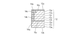
<実施例2> 実施例1の電子部品10aについて、図5及び図6を参照しながら説明する。
Example 2 An electronic component 10a of Example 1 will be described with reference to FIGS.
図5は、電子部品10aの外観を示す概略図である。図6は、図5の線A-Aに沿って切断した要部断面図である。
FIG. 5 is a schematic view showing the appearance of the electronic component 10a. FIG. 6 is a cross-sectional view of a principal part taken along line AA in FIG.
図5及び図6に示すように、電子部品10aは、実施例1の電子部品10と略同様に構成されている。以下では、実施例1と同様の構成部分には同じ符号を用い、相違点を中心に説明する。
As shown in FIGS. 5 and 6, the electronic component 10a is configured in substantially the same manner as the electronic component 10 of the first embodiment. Below, the same code | symbol is used for the component similar to Example 1, and it demonstrates centering around difference.
電子部品10aは、絶縁層12p~12wが積層された本体12の一方の主面12aにのみ、主面導体16cが形成されている。主面導体16cが形成されている絶縁層12pに形成された最外導体14cは、主面導体16cが形成された絶縁層12pの外周端面(すなわち、本体12の側面12c)に露出し、かつ、積層方向から見たとき、側面導体14kに重なり、かつ側面導体14kの外側にはみ出ている。
In the electronic component 10a, the main surface conductor 16c is formed only on one main surface 12a of the main body 12 on which the insulating layers 12p to 12w are laminated. The outermost conductor 14c formed on the insulating layer 12p on which the main surface conductor 16c is formed is exposed on the outer peripheral end surface (that is, the side surface 12c of the main body 12) of the insulating layer 12p on which the main surface conductor 16c is formed, and When viewed from the stacking direction, it overlaps the side conductor 14k and protrudes outside the side conductor 14k.
例えば、積層方向から見たとき、最外導体14cと側面導体14kとは、同心に配置された径の異なる円を分割した略半円形状を有し、最外導体14cの外径は側面導体14kの外径よりも大きい。
For example, when viewed from the stacking direction, the outermost conductor 14c and the side conductor 14k have a substantially semicircular shape obtained by dividing circles having different diameters arranged concentrically, and the outer diameter of the outermost conductor 14c is the side conductor. It is larger than the outer diameter of 14k.
側面導体14kは、主面導体16cが形成された絶縁層12pに隣接する絶縁層12qと、本体12内の中間位置の絶縁層12tとの間の絶縁層12p~12tに連続して形成されている。側面導体14kの一方の端部14pは、最外導体14cに接続されている。側面導体14kの他方の端部14qは、本体12内の中間位置の絶縁層12t,12uの間に形成された配線導体15cに接続されている。
The side conductor 14k is continuously formed on the insulating layers 12p to 12t between the insulating layer 12q adjacent to the insulating layer 12p on which the main surface conductor 16c is formed and the insulating layer 12t at the intermediate position in the main body 12. Yes. One end 14p of the side conductor 14k is connected to the outermost conductor 14c. The other end 14q of the side conductor 14k is connected to a wiring conductor 15c formed between the insulating layers 12t and 12u at an intermediate position in the main body 12.
側面導体14kと主面導体16cとは、最外導体14cを介して電気的に接続されている。主面導体16cと最外導体14cとは、積層方向から見たときに側面導体14kよりも本体12の内側の位置でも接続されている。このように、本体12の側面12cと主面12aが交わる角部12mから離れた位置に、主面導体16cと最外導体15cとが接続される部分を設けることにより、主面導体16cと最外導体14cとの接続を断線しにくくすることができる。これによって、側面導体14kと主面導体16cとの電気的接続の信頼性が向上する。
The side conductor 14k and the main conductor 16c are electrically connected via the outermost conductor 14c. The main surface conductor 16c and the outermost conductor 14c are connected to each other at a position inside the main body 12 relative to the side surface conductor 14k when viewed from the stacking direction. Thus, by providing a portion where the main surface conductor 16c and the outermost conductor 15c are connected at a position away from the corner 12m where the side surface 12c of the main body 12 and the main surface 12a intersect, the main surface conductor 16c and the outermost conductor 16c are provided. It is possible to make it difficult to disconnect the connection with the outer conductor 14c. This improves the reliability of electrical connection between the side conductors 14k and the main conductor 16c.
最外導体14cと側面導体14kは、最外導体14cと側面導体14kとを接続する配線導体を介さずに接続されるので、電子部品10aの構成が簡単になる。
Since the outermost conductor 14c and the side conductor 14k are connected without a wiring conductor connecting the outermost conductor 14c and the side conductor 14k, the configuration of the electronic component 10a is simplified.
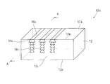
<比較例> 比較例の電子部品10xについて、図7~図9を参照しながら説明する。
<Comparative Example> An electronic component 10x of a comparative example will be described with reference to FIGS.
図7は、電子部品10xの外観を示す概略図である。図8及び図9は、図7の線A-Aに沿って切断した要部断面図である。
FIG. 7 is a schematic diagram showing the external appearance of the electronic component 10x. 8 and 9 are cross-sectional views of the main part taken along line AA in FIG.
図7及び図8に示すように、電子部品10xは、本体12の全ての絶縁層に側面導体14xが形成されている。側面導体14xの両端14y,14zには、本体12の主面12a,12bに形成された主面導体16x,16yの端部16p,16qが接続されている。すなわち、主面導体16x,16yの端部16p,16qは、本体12の角部12m,12nに達するように形成され、本体12の角部12m,12nの近傍で側面導体14xと接続されている。
7 and 8, in the electronic component 10x, side conductors 14x are formed on all the insulating layers of the main body 12. Ends 16p and 16q of main surface conductors 16x and 16y formed on main surfaces 12a and 12b of the main body 12 are connected to both ends 14y and 14z of the side conductor 14x. That is, the end portions 16p and 16q of the main surface conductors 16x and 16y are formed so as to reach the corner portions 12m and 12n of the main body 12, and are connected to the side conductors 14x in the vicinity of the corner portions 12m and 12n of the main body 12. .
主面導体16x,16yの端部16p,16qは、本体12の角部12m,12nの近傍に形成される。本体12の角部12m,12nの近傍は、電子部品10xを回路基板に実装するまでの間に、最も擦れやすい部分であるため、薄くなったり剥がれたりして、主面導体16x,16yの端部16p,16qは、図9に模式的に示すように断線しやすい。
The end portions 16p and 16q of the main surface conductors 16x and 16y are formed in the vicinity of the corner portions 12m and 12n of the main body 12. The vicinity of the corner portions 12m and 12n of the main body 12 is the portion that is most easily rubbed before the electronic component 10x is mounted on the circuit board. Therefore, the main body 12 is thinned or peeled off, and ends of the main surface conductors 16x and 16y. The parts 16p and 16q are easily disconnected as schematically shown in FIG.
これに対し、実施例1及び実施例2のように、主面導体が接続される部分が、本体の角部の近傍から離れていると、断線しにくい。
On the other hand, if the part to which the main surface conductor is connected is away from the vicinity of the corner of the main body as in Example 1 and Example 2, it is difficult to disconnect.
<まとめ> 以上に説明したように、主面導体と最外導体とが、積層方向から見たときに側面導体よりも本体の内側において互いに接続される部分を含むように構成することによって、被覆層を形成することなく、側面導体と主面導体との電気的接続の信頼性を向上することができる。
<Summary> As described above, the main surface conductor and the outermost conductor are configured so as to include a portion connected to each other inside the main body rather than the side surface conductor when viewed from the stacking direction. The reliability of the electrical connection between the side conductor and the main conductor can be improved without forming a layer.
なお、本発明は、上記実施の形態に限定されるものではなく、種々変更を加えて実施することが可能である。
It should be noted that the present invention is not limited to the above embodiment, and can be implemented with various modifications.
例えば、本体の絶縁層は、セラミックに限らず、樹脂等で形成しても構わない。
For example, the insulating layer of the main body is not limited to ceramic but may be formed of resin or the like.
10,10a,10k,10x 電子部品
12 本体
12a,12b 主面
12c,12d 側面
12e,12f 端面
12m,12n 角部
12p~12w 絶縁層
14 側面導体
14a,14b,14c 最外導体
14g~14i,14k,14u~14w,14x 側面導体
15a,15b,15c 配線導体
16a,16b,16c,16g~16j,16u~16w,16x,16y 主面導体
24g~24i,24u~24w 最外導体
25g~25i,25u~25w 最外導体
26g~26i,26u~26w 配線導体
27g~27i,27u~27w 配線導体 10, 10a, 10k,10x Electronic component 12 Main body 12a, 12b Main surface 12c, 12d Side surface 12e, 12f End surface 12m, 12n Corner portion 12p-12w Insulating layer 14 Side surface conductors 14a, 14b, 14c Outermost conductors 14g-14i, 14k , 14u to 14w, 14x Side conductors 15a, 15b, 15c Wiring conductors 16a, 16b, 16c, 16g to 16j, 16u to 16w, 16x, 16y Main surface conductors 24g to 24i, 24u to 24w Outermost conductors 25g to 25i, 25u ~ 25w Outermost conductor 26g ~ 26i, 26u ~ 26w Wiring conductor 27g ~ 27i, 27u ~ 27w Wiring conductor
12 本体
12a,12b 主面
12c,12d 側面
12e,12f 端面
12m,12n 角部
12p~12w 絶縁層
14 側面導体
14a,14b,14c 最外導体
14g~14i,14k,14u~14w,14x 側面導体
15a,15b,15c 配線導体
16a,16b,16c,16g~16j,16u~16w,16x,16y 主面導体
24g~24i,24u~24w 最外導体
25g~25i,25u~25w 最外導体
26g~26i,26u~26w 配線導体
27g~27i,27u~27w 配線導体 10, 10a, 10k,
Claims (6)
- 互いに積層された複数の絶縁層を含む本体と、
前記絶縁層が積層された積層方向の少なくとも片側の前記本体の主面に形成された主面導体と、
互いに隣接する前記絶縁層を貫通し、前記絶縁層の外周端面に露出し、前記主面導体が形成された前記絶縁層に達するように連続して形成された側面導体と、
前記主面導体が形成された前記絶縁層を貫通し、少なくとも一部が、前記絶縁層が積層された積層方向から見たときに前記側面導体よりも前記本体の内側に配置された最外導体と、
を備え、
前記主面導体と前記側面導体とが、前記最外導体を介して電気的に接続されていることを特徴とする、電子部品。 A body including a plurality of insulating layers stacked on each other;
A main surface conductor formed on the main surface of the main body on at least one side in the stacking direction in which the insulating layers are stacked;
Side conductors that pass through the insulating layers adjacent to each other, are exposed at the outer peripheral end surface of the insulating layer, and are continuously formed so as to reach the insulating layer on which the main surface conductor is formed,
The outermost conductor that penetrates the insulating layer on which the main surface conductor is formed and that is at least partially disposed on the inner side of the main body than the side conductor when viewed from the stacking direction in which the insulating layer is stacked When,
With
The electronic component, wherein the main surface conductor and the side surface conductor are electrically connected via the outermost conductor. - 前記最外導体の全部が、前記絶縁層の積層方向から見たときに前記側面導体よりも前記本体の内側に配置され、
前記主面導体が形成された前記絶縁層と、該絶縁層に隣接する前記絶縁層との間に、前記最外導体と前記側面導体とを電気的に接続する配線導体が形成されていることを特徴とする、請求項1に記載の電子部品。 All of the outermost conductor is disposed inside the main body rather than the side conductor when viewed from the stacking direction of the insulating layer,
A wiring conductor that electrically connects the outermost conductor and the side conductor is formed between the insulating layer on which the main surface conductor is formed and the insulating layer adjacent to the insulating layer. The electronic component according to claim 1, wherein: - 前記最外導体は、前記主面導体が形成された前記絶縁層の外周端面に露出し、前記積層方向から見たとき、前記側面導体に重なり、かつ前記側面導体の外側にはみ出ていることを特徴とする、請求項1に記載の電子部品。 The outermost conductor is exposed on an outer peripheral end surface of the insulating layer on which the main surface conductor is formed, and overlaps with the side conductor and protrudes outside the side conductor when viewed from the stacking direction. The electronic component according to claim 1, wherein the electronic component is characterized.
- 前記積層方向から見たとき、前記主面導体と前記最外導体とは、同心に配置された外径の異なる円を分割した形状を有することを特徴とする、請求項3に記載の電子部品。 4. The electronic component according to claim 3, wherein the main surface conductor and the outermost conductor have a shape obtained by dividing a concentrically arranged circle having different outer diameters when viewed from the stacking direction. .
- 前記側面導体及び前記最外導体が貫通する前記絶縁層が、磁性体セラミック材料を含むことを特徴とする、請求項1乃至4のいずれか一つに記載の電子部品。 The electronic component according to any one of claims 1 to 4, wherein the insulating layer through which the side conductor and the outermost conductor penetrate includes a magnetic ceramic material.
- 互いに電気的に接続された前記主面導体と前記側面導体と前記最外導体とによりコイル導体が形成されたインダクタ素子であることを特徴とする、請求項5に記載の電子部品。 The electronic component according to claim 5, wherein the electronic component is an inductor element in which a coil conductor is formed by the main surface conductor, the side surface conductor, and the outermost conductor electrically connected to each other.
Priority Applications (1)
| Application Number | Priority Date | Filing Date | Title |
|---|---|---|---|
| JP2013504674A JP5445884B2 (en) | 2011-03-16 | 2012-03-07 | Electronic components |
Applications Claiming Priority (2)
| Application Number | Priority Date | Filing Date | Title |
|---|---|---|---|
| JP2011-057557 | 2011-03-16 | ||
| JP2011057557 | 2011-03-16 |
Publications (1)
| Publication Number | Publication Date |
|---|---|
| WO2012124561A1 true WO2012124561A1 (en) | 2012-09-20 |
Family
ID=46830634
Family Applications (1)
| Application Number | Title | Priority Date | Filing Date |
|---|---|---|---|
| PCT/JP2012/055786 WO2012124561A1 (en) | 2011-03-16 | 2012-03-07 | Electronic part |
Country Status (2)
| Country | Link |
|---|---|
| JP (1) | JP5445884B2 (en) |
| WO (1) | WO2012124561A1 (en) |
Cited By (3)
| Publication number | Priority date | Publication date | Assignee | Title |
|---|---|---|---|---|
| WO2015005160A1 (en) * | 2013-07-11 | 2015-01-15 | 株式会社村田製作所 | Electronic component, communication module, and electronic apparatus |
| JP2017120886A (en) * | 2015-12-29 | 2017-07-06 | サムソン エレクトロ−メカニックス カンパニーリミテッド. | Multilayer electronic component and multilayer chip antenna |
| JPWO2016121491A1 (en) * | 2015-01-30 | 2017-10-05 | 株式会社村田製作所 | Electronic circuit module |
Families Citing this family (1)
| Publication number | Priority date | Publication date | Assignee | Title |
|---|---|---|---|---|
| KR102429685B1 (en) | 2017-07-05 | 2022-08-05 | 삼성전기주식회사 | Thin film type inductor |
Citations (6)
| Publication number | Priority date | Publication date | Assignee | Title |
|---|---|---|---|---|
| JPH0730356A (en) * | 1993-07-12 | 1995-01-31 | Takeshi Ikeda | Noise filter |
| JPH10208941A (en) * | 1997-01-17 | 1998-08-07 | Citizen Electron Co Ltd | Chip inductor and its manufacture |
| JP2003078377A (en) * | 2001-08-30 | 2003-03-14 | Fdk Corp | Lc combined chip component |
| JP2005167098A (en) * | 2003-12-04 | 2005-06-23 | Murata Mfg Co Ltd | Laminated ceramic electronic component |
| JP2007019891A (en) * | 2005-07-07 | 2007-01-25 | Toda Kogyo Corp | Magnetic antenna |
| WO2009147899A1 (en) * | 2008-06-06 | 2009-12-10 | 株式会社村田製作所 | Electronic part and method for manufacturing the same |
-
2012
- 2012-03-07 JP JP2013504674A patent/JP5445884B2/en active Active
- 2012-03-07 WO PCT/JP2012/055786 patent/WO2012124561A1/en active Application Filing
Patent Citations (6)
| Publication number | Priority date | Publication date | Assignee | Title |
|---|---|---|---|---|
| JPH0730356A (en) * | 1993-07-12 | 1995-01-31 | Takeshi Ikeda | Noise filter |
| JPH10208941A (en) * | 1997-01-17 | 1998-08-07 | Citizen Electron Co Ltd | Chip inductor and its manufacture |
| JP2003078377A (en) * | 2001-08-30 | 2003-03-14 | Fdk Corp | Lc combined chip component |
| JP2005167098A (en) * | 2003-12-04 | 2005-06-23 | Murata Mfg Co Ltd | Laminated ceramic electronic component |
| JP2007019891A (en) * | 2005-07-07 | 2007-01-25 | Toda Kogyo Corp | Magnetic antenna |
| WO2009147899A1 (en) * | 2008-06-06 | 2009-12-10 | 株式会社村田製作所 | Electronic part and method for manufacturing the same |
Cited By (4)
| Publication number | Priority date | Publication date | Assignee | Title |
|---|---|---|---|---|
| WO2015005160A1 (en) * | 2013-07-11 | 2015-01-15 | 株式会社村田製作所 | Electronic component, communication module, and electronic apparatus |
| JPWO2016121491A1 (en) * | 2015-01-30 | 2017-10-05 | 株式会社村田製作所 | Electronic circuit module |
| JP2017120886A (en) * | 2015-12-29 | 2017-07-06 | サムソン エレクトロ−メカニックス カンパニーリミテッド. | Multilayer electronic component and multilayer chip antenna |
| US10374313B2 (en) | 2015-12-29 | 2019-08-06 | Samsung Electro-Mechanics Co., Ltd. | Multilayer electronic component and multilayer chip antenna including the same |
Also Published As
| Publication number | Publication date |
|---|---|
| JPWO2012124561A1 (en) | 2014-07-24 |
| JP5445884B2 (en) | 2014-03-19 |
Similar Documents
| Publication | Publication Date | Title |
|---|---|---|
| JP5196038B2 (en) | Coil built-in board | |
| JP4929487B2 (en) | Multilayer ceramic electronic components | |
| CN103703524B (en) | Electronic unit and manufacture method thereof | |
| JP4682890B2 (en) | Multilayer noise filter | |
| JP5621573B2 (en) | Coil built-in board | |
| JP5445884B2 (en) | Electronic components | |
| JP4034787B2 (en) | Stacked balun transformer | |
| JP2006294724A (en) | Composite electronic component and its manufacturing method | |
| WO2010032464A1 (en) | Laminated electronic component | |
| WO2016132666A1 (en) | Common mode noise filter | |
| WO2014115433A1 (en) | Coil component and electronic device | |
| JP6753091B2 (en) | Laminated common mode filter | |
| KR101158220B1 (en) | Multi-layer Inductor | |
| JP2010192643A (en) | Common mode noise filter | |
| JP2001076952A (en) | Laminated ceramic electronic component and manufacture thereof | |
| JP6354220B2 (en) | Multilayer electronic components | |
| JP4295660B2 (en) | Balun transformer | |
| JP4216856B2 (en) | Multilayer electronic components | |
| JP2005333012A5 (en) | ||
| WO2011132476A1 (en) | Electronic component with laminated substrate | |
| JP2007067982A (en) | Filter element | |
| JP2013041886A (en) | Laminated feedthrough capacitor | |
| JP2018098701A (en) | Balance-unbalance converter | |
| JP5277918B2 (en) | Surge absorber and manufacturing method thereof | |
| JP2013157584A (en) | Common mode noise filter |
Legal Events
| Date | Code | Title | Description |
|---|---|---|---|
| 121 | Ep: the epo has been informed by wipo that ep was designated in this application |
Ref document number: 12757414 Country of ref document: EP Kind code of ref document: A1 |
|
| ENP | Entry into the national phase |
Ref document number: 2013504674 Country of ref document: JP Kind code of ref document: A |
|
| NENP | Non-entry into the national phase |
Ref country code: DE |
|
| 122 | Ep: pct application non-entry in european phase |
Ref document number: 12757414 Country of ref document: EP Kind code of ref document: A1 |