WO2012120878A1 - Dispositif de correction d'équilibre, et système de stockage d'électricité - Google Patents
Dispositif de correction d'équilibre, et système de stockage d'électricité Download PDFInfo
- Publication number
- WO2012120878A1 WO2012120878A1 PCT/JP2012/001537 JP2012001537W WO2012120878A1 WO 2012120878 A1 WO2012120878 A1 WO 2012120878A1 JP 2012001537 W JP2012001537 W JP 2012001537W WO 2012120878 A1 WO2012120878 A1 WO 2012120878A1
- Authority
- WO
- WIPO (PCT)
- Prior art keywords
- storage cell
- inductor
- switching element
- balance correction
- power storage
- Prior art date
Links
Images


Classifications
-
- H—ELECTRICITY
- H01—ELECTRIC ELEMENTS
- H01M—PROCESSES OR MEANS, e.g. BATTERIES, FOR THE DIRECT CONVERSION OF CHEMICAL ENERGY INTO ELECTRICAL ENERGY
- H01M10/00—Secondary cells; Manufacture thereof
- H01M10/42—Methods or arrangements for servicing or maintenance of secondary cells or secondary half-cells
- H01M10/425—Structural combination with electronic components, e.g. electronic circuits integrated to the outside of the casing
-
- H—ELECTRICITY
- H02—GENERATION; CONVERSION OR DISTRIBUTION OF ELECTRIC POWER
- H02J—CIRCUIT ARRANGEMENTS OR SYSTEMS FOR SUPPLYING OR DISTRIBUTING ELECTRIC POWER; SYSTEMS FOR STORING ELECTRIC ENERGY
- H02J7/00—Circuit arrangements for charging or depolarising batteries or for supplying loads from batteries
- H02J7/0013—Circuit arrangements for charging or depolarising batteries or for supplying loads from batteries acting upon several batteries simultaneously or sequentially
- H02J7/0014—Circuits for equalisation of charge between batteries
- H02J7/0016—Circuits for equalisation of charge between batteries using shunting, discharge or bypass circuits
-
- H—ELECTRICITY
- H01—ELECTRIC ELEMENTS
- H01M—PROCESSES OR MEANS, e.g. BATTERIES, FOR THE DIRECT CONVERSION OF CHEMICAL ENERGY INTO ELECTRICAL ENERGY
- H01M10/00—Secondary cells; Manufacture thereof
- H01M10/42—Methods or arrangements for servicing or maintenance of secondary cells or secondary half-cells
- H01M10/425—Structural combination with electronic components, e.g. electronic circuits integrated to the outside of the casing
- H01M2010/4271—Battery management systems including electronic circuits, e.g. control of current or voltage to keep battery in healthy state, cell balancing
-
- H—ELECTRICITY
- H02—GENERATION; CONVERSION OR DISTRIBUTION OF ELECTRIC POWER
- H02J—CIRCUIT ARRANGEMENTS OR SYSTEMS FOR SUPPLYING OR DISTRIBUTING ELECTRIC POWER; SYSTEMS FOR STORING ELECTRIC ENERGY
- H02J2310/00—The network for supplying or distributing electric power characterised by its spatial reach or by the load
- H02J2310/40—The network being an on-board power network, i.e. within a vehicle
-
- Y—GENERAL TAGGING OF NEW TECHNOLOGICAL DEVELOPMENTS; GENERAL TAGGING OF CROSS-SECTIONAL TECHNOLOGIES SPANNING OVER SEVERAL SECTIONS OF THE IPC; TECHNICAL SUBJECTS COVERED BY FORMER USPC CROSS-REFERENCE ART COLLECTIONS [XRACs] AND DIGESTS
- Y02—TECHNOLOGIES OR APPLICATIONS FOR MITIGATION OR ADAPTATION AGAINST CLIMATE CHANGE
- Y02E—REDUCTION OF GREENHOUSE GAS [GHG] EMISSIONS, RELATED TO ENERGY GENERATION, TRANSMISSION OR DISTRIBUTION
- Y02E60/00—Enabling technologies; Technologies with a potential or indirect contribution to GHG emissions mitigation
- Y02E60/10—Energy storage using batteries
-
- Y—GENERAL TAGGING OF NEW TECHNOLOGICAL DEVELOPMENTS; GENERAL TAGGING OF CROSS-SECTIONAL TECHNOLOGIES SPANNING OVER SEVERAL SECTIONS OF THE IPC; TECHNICAL SUBJECTS COVERED BY FORMER USPC CROSS-REFERENCE ART COLLECTIONS [XRACs] AND DIGESTS
- Y02—TECHNOLOGIES OR APPLICATIONS FOR MITIGATION OR ADAPTATION AGAINST CLIMATE CHANGE
- Y02T—CLIMATE CHANGE MITIGATION TECHNOLOGIES RELATED TO TRANSPORTATION
- Y02T10/00—Road transport of goods or passengers
- Y02T10/60—Other road transportation technologies with climate change mitigation effect
- Y02T10/70—Energy storage systems for electromobility, e.g. batteries
Definitions
- the present invention relates to a balance correction device and a power storage system.
- Patent Documents 1 to 3 a balance correction circuit that includes an inductor, a switching element, and a drive circuit for the switching element and that equalizes the voltage between the storage cells has been proposed (see Patent Documents 1 to 3).
- Patent Literature Patent Document 1 JP 2006-067748 (Patent Document 2) JP 2008-017655 (Patent Document 3) JP 2009-232660
- an object of one aspect of the present invention is to provide a balance correction device and a power storage system that can solve the above-described problems. This object is achieved by a combination of features described in the independent claims.
- the dependent claims define further advantageous specific examples of the present invention.
- a balance correction device for equalizing voltages of a first power storage cell and a second power storage cell connected in series, wherein one end of the first power storage cell and the second power storage cell An inductor having one end electrically connected to a connection point with one end of the storage cell, and a first switching element electrically connected between the other end of the inductor and the other end of the first storage cell; A second switching element electrically connected between the other end of the inductor and the other end of the second storage cell, and a series of the inductors connected in series, and the magnitude of the current flowing through the inductor is predetermined.
- a balance correction device including a current limiting element that limits a current flowing through the inductor is provided.
- the current limiting element is between a connection point of one end of the first storage cell and one end of the second storage cell and a connection point of the first switching element and the second switching element.
- the inductor may be connected in series.
- the current limiting element includes a first current limiting element connected in series with the inductor between the other end of the first storage cell and the first switching element, and a second You may have the 2nd current limiting element connected in series with an inductor between the other end of an electrical storage cell, and a 2nd switching element.
- the current limiting element may be a fuse.
- the fuse may be an overcurrent interruption type fuse or a thermal fuse.
- An example of apparatus 100 provided with accumulation-of-electricity system 110 is shown roughly.
- An example of the electrical storage system 210 is shown schematically.
- movement of the electrical storage system 210 is shown schematically.
- An example of the electrical storage system 410 is shown schematically.
- FIG. 1 schematically shows an example of a device 100 including a power storage system 110.
- Device 100 includes a motor 102 and a power storage system 110.
- the device 100 may be a transportation device such as an electric vehicle, a hybrid vehicle, an electric motorcycle, a railway vehicle, and an elevator.
- the device 100 may be an electrical device such as a PC or a mobile phone.
- the motor 102 is electrically connected to the power storage system 110 and uses power supplied from the power storage system 110.
- the motor 102 may be used as a regenerative brake.
- the motor 102 may be an example of a power load.
- the power storage system 110 is electrically connected to the motor 102 and supplies power to the motor 102 (sometimes referred to as discharging of the power storage system).
- the power storage system 110 is electrically connected to a charging device (not shown) and stores electrical energy (sometimes referred to as charging of the power storage system).
- the power storage system 110 includes a terminal 112, a terminal 114, a plurality of power storage cells connected in series including a power storage cell 122, a power storage cell 124, a power storage cell 126, and a power storage cell 128, a balance correction circuit 132, and a balance correction circuit 134. And a plurality of balance correction circuits including a balance correction circuit 136.
- the balance correction circuit 132, the balance correction circuit 134, and the balance correction circuit 136 may be an example of a balance correction device.
- electrically connected is not limited to a case where a certain element is directly connected to another element.
- a third element may be interposed between one element and another element.
- it is not limited to when a certain element and another element are physically connected.
- the input winding and output winding of the transformer are not physically connected, but are electrically connected.
- an element and another element are electrically connected. Including the case of connection.
- “connected in series” indicates that one element and another element are electrically connected in series.
- the terminals 112 and 114 electrically connect the power storage system 110 to devices outside the system such as the motor 102 and the charging device.
- Power storage cell 122, power storage cell 124, power storage cell 126, and power storage cell 128 are connected in series.
- the power storage cell 122, the power storage cell 124, the power storage cell 126, and the power storage cell 128 may be secondary batteries or capacitors.
- the storage cell 124, the storage cell 126, and the storage cell 128 may be lithium ion batteries.
- Each of power storage cell 122, power storage cell 124, power storage cell 126, and power storage cell 128 may include a plurality of power storage cells.
- battery characteristics include battery capacity or discharge voltage characteristics indicating the relationship of battery voltage to discharge time. For example, as the storage cell deteriorates, the battery voltage decreases with a shorter discharge time.
- the storage cell 122 and the storage cell 124 have a predetermined range of charge levels (sometimes referred to as “State of Charge” or “SOC”), when the voltages of the storage cell 122 and the storage cell 124 vary.
- SOC state of Charge
- the utilization efficiency of the power storage system 110 is deteriorated. Therefore, the use efficiency of the power storage system 110 can be improved by equalizing the voltages of the power storage cell 122 and the power storage cell 124.
- the balance correction circuit 132 equalizes the voltages of the storage cell 122 and the storage cell 124.
- the balance correction circuit 132 includes one end (sometimes referred to as a positive electrode side) of the storage cell 122 on the terminal 112 side, one end (sometimes referred to as a negative electrode side) on the terminal 114 side of the storage cell 122, and the positive electrode of the storage cell 124. It is electrically connected to the connection point 143 with the side.
- the balance correction circuit 132 is electrically connected to a connection point 143 and a connection point 145 between the negative electrode side of the storage cell 124 and the positive electrode side of the storage cell 126.
- the balance correction circuit 132 may include an inductor that is electrically connected to the connection point 143.
- the balance correction circuit 132, the storage cell 122, and the storage cell 124 are electrically connected as described above, so that the first circuit including the storage cell 122 and the inductor, the storage cell 124, and the inductor A second circuit including is formed.
- the balance correction circuit 132 causes a current to flow alternately through the first circuit and the second circuit. Thereby, electrical energy can be transferred between the storage cell 122 and the storage cell 124 via the inductor. As a result, the voltages of the storage cell 122 and the storage cell 124 can be equalized.
- the balance correction circuit 134 equalizes the voltages of the storage cell 124 and the storage cell 126.
- the balance correction circuit 134 is electrically connected to a connection point 143, a connection point 145, and a connection point 147 between the negative electrode side of the storage cell 126 and the positive electrode side of the storage cell 128.
- the balance correction circuit 136 equalizes the voltages of the storage cell 126 and the storage cell 128.
- the balance correction circuit 136 is electrically connected to the connection point 145, the connection point 147, and the negative electrode side of the storage cell 128.
- the balance correction circuit 134 and the balance correction circuit 136 may have the same configuration as the balance correction circuit 132.
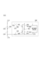
- FIG. 2 schematically shows an example of the power storage system 210.
- the power storage system 210 includes a terminal 212, a terminal 214, a power storage cell 222 and a power storage cell 224 connected in series, and a balance correction circuit 232.
- the balance correction circuit 232 may be an example of a balance correction device.
- the power storage cell 222 may be an example of a first power storage cell.
- the power storage cell 224 may be an example of a second power storage cell.
- the terminal 212 and the terminal 214 may have the same configuration as the terminal 112 and the terminal 114 of the power storage system 110, respectively.
- the power storage cell 222 and the power storage cell 224 may have the same configuration as the power storage cell 122, the power storage cell 124, the power storage cell 126, or the power storage cell 128.
- the power storage system 110 may have a configuration similar to that of the power storage system 210.
- the balance correction circuit 132, the balance correction circuit 134, and the balance correction circuit 136 may have the same configuration as the balance correction circuit 232.
- the balance correction circuit 232 equalizes the voltages of the storage cell 222 and the storage cell 224.
- the balance correction circuit 232 includes an inductor 250, a switching element 252, a switching element 254, a control signal generation unit 272, a diode 282, a diode 284, and a fuse 290.
- the switching element 252 may be an example of a first switching element.
- the switching element 254 may be an example of a second switching element.
- the fuse 290 may be an example of a current limiting element.
- the balance correction circuit 232 is electrically connected to the positive electrode side of the energy storage cell 222 and the connection point 243 between the negative electrode side of the energy storage cell 222 and the positive electrode side of the energy storage cell 224.
- a first switching circuit including the storage cell 222, the switching element 252, the fuse 290, and the inductor 250 is formed.
- the balance correction circuit 232 is electrically connected to the connection point 243 and the negative electrode side of the storage cell 224.
- a second switching circuit including the storage cell 224, the inductor 250, the fuse 290, and the switching element 254 is formed.
- the connection point 243 may be an example of a connection point between one end of the first power storage cell and one end of the second power storage cell.
- One end of the inductor 250 is electrically connected to the connection point 243.
- the other end of the inductor 250 may be electrically connected to a connection point 263 between the switching element 252 and the switching element 254.
- an inductor current IL is generated in the inductor 250.
- the switching element 252 is electrically connected between the other end of the inductor 250 and the positive electrode side of the storage cell 222.
- the switching element 252 receives the control signal ⁇ 22 from the control signal generator 272, and performs an on operation or an off operation based on the control signal ⁇ 22. This opens and closes the first open / close circuit.
- the switching element 252 may be a MOSFET.
- the switching element 254 is electrically connected between the other end of the inductor 250 and the negative electrode side of the storage cell 224.
- the switching element 254 receives the control signal ⁇ 24 from the control signal generator 272 and performs an on operation or an off operation based on the control signal ⁇ 24. As a result, the second open / close circuit is opened and closed.
- the switching element 254 may be a MOSFET.
- the control signal generator 272 generates a control signal ⁇ 22 that controls the on / off operation of the switching element 252 and a control signal ⁇ 24 that controls the on / off operation of the switching element 254.
- the control signal generator 272 supplies the control signal ⁇ 22 to the switching element 252.
- the control signal generator 272 supplies the control signal ⁇ 24 to the switching element 254.
- the control signal generation unit 272 may generate the control signal ⁇ 22 and the control signal ⁇ 24 so that the switching element 252 and the switching element 254 repeat ON / OFF operations alternately. Thereby, the switching element 252 and the switching element 254 can be alternately turned on and off.
- Control signal ⁇ 22 and control signal ⁇ 24 may each be a square wave with a duty ratio of 50%. The duty ratio can be calculated as the ratio of the ON period to the period of the square wave.
- the control signal generator 272 may be a pulse generator that generates a pulse train having a predetermined cycle.
- Control signal generator 272 may be a variable pulse generator that variably controls the duty ratio of at least one of control signal ⁇ 22 and control signal ⁇ 24.
- the control signal generator 272 may be formed on the same substrate as the switching element 252 and the switching element 254.
- the diode 282 is arranged in parallel with the switching element 252 and allows a current to flow in the direction from the other end of the inductor 250 to the positive electrode side of the storage cell 222.
- the diode 284 is arranged in parallel with the switching element 254 and allows a current to flow in the direction from the negative electrode side of the storage cell 224 to the other end of the inductor 250.
- the diode 282 and the diode 284 may be parasitic diodes formed equivalently between the source and drain of the MOSFET.
- the inductor current I L diode 282 or diode 284 can continue to flow through.
- the inductor current I L generated once the inductor 250 can be utilized without waste. Further, it is possible to suppress the generation of a surge voltage that occurs when the inductor current IL is cut off.
- the fuse 290 is connected to the inductor 250 in series.
- one end of the fuse 290 is electrically connected to the other end of the inductor 250.
- the other end of the fuse 290 is electrically connected to a connection point 263 between the switching element 252 and the switching element 254.
- the fuse 290 limits the current flowing through the inductor 250 when the magnitude of the current flowing through the inductor 250 exceeds a predetermined value.
- the storage cell 222 and the storage cell 224 can be protected.
- an arbitrary balance correction circuit 232 is extracted for the purpose of confirming that the safety of the power storage system 210 can be ensured even if the semiconductor element should fail.
- an open / short test is performed. Even when at least one of the switching element 252 and the switching element 254 is closed in the open / short test, since the fuse 290 is connected in series to the inductor 250, the storage cell 222 and the storage cell 224 are protected. can do. As a result, the safety of the power storage system 210 can be ensured.
- the fuse 290 is disposed between the other end of the inductor 250 and the connection point 263 .
- the number or installation location of the fuses 290 is not limited to this.
- the fuse 290 may be connected in series to the inductor 250 between the connection point 243 and one end of the inductor 250. Thereby, both the electrical storage cell 222 and the electrical storage cell 224 can be protected by a single fuse.
- the fuse 290 may be an overcurrent interruption type fuse or a thermal fuse. In the present embodiment, the case where a fuse is used as the current limiting element has been described. However, the current limiting element is not limited to this.
- the current limiting element may be a PTC thermistor whose internal resistance increases as the temperature rises.
- the current limiting element may be an electric current breaker.
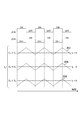
- FIG. 3 schematically shows an example of the operation of the power storage system 210.
- FIG. 3 shows a graph 302, a graph 304, and a graph 306 in association with examples of the waveforms of the control signal ⁇ 22 and the control signal ⁇ 24.
- the horizontal axis indicates the passage of time.
- the vertical axis shows the magnitude of the inductor current I L.
- the magnitude of the inductor current I L represents the current flowing from the connection point 263 toward the connecting point 243 (. Indicated by the solid line arrow in FIG. 2) as a positive.
- Graph 302 illustrates an example of a temporal change of the inductor current I L when the voltage E 2 of the energy storage cell 222 is greater than the voltage E 4 of the electric storage cell 224 schematically.
- Graph 304 illustrates an example of a temporal change of the inductor current I L when the voltage E 2 of the energy storage cell 222 is smaller than the voltage E 4 of the electric storage cell 224 schematically.
- Graph 306 illustrates an example of a temporal change of the inductor current I L when the voltage E 2 of the energy storage cell 222 and the voltage E 4 storage cells 224 are substantially the same schematically.
- control signal ⁇ 22 and the control signal ⁇ 24 are square waves having a duty ratio of 50%. As shown in FIG. 3, control signal ⁇ 22 and control signal ⁇ 24 have complementary logic or phase polarities so that one of switching element 252 and switching element 254 is in the off state while the other is in the on state.
- the switching element 252 is turned off, the switching element 254 is turned on, the inductor current I L is charged in the inductor 250 of the inductor 250 at one end - the connection point 243- storage cell 224-switching element 254- connection It is discharged in the current path at point 263-fuse 290-inductor 250 at the other end. This discharge is performed while charging the storage cell 224. As shown in FIG. 3, the inductor current I L decreases with time due to the discharge, the discharge current becomes zero, the inductor 250, to flow the opposite direction of the charge current and the discharge current.
- the fuse 290 is blown and the current flowing through the inductor 250 is limited. . Thereby, the electrical storage cell 222 can be protected.
- the switching element 254 is turned off, the switching element 252 is turned on, the other end of the inductor current I L inductor 250 charged in the inductor 250 - Fuse 290- connection point 263- switching element 25 2 energy storage
- an overcurrent may flow between the connection point 243 and the connection point 263.
- the fuse 290 is blown and the current flowing through the inductor 250 is limited. . Thereby, the electrical storage cell 224 can be protected.
- the balance correction circuit 232 causes a current to flow alternately between the first switching circuit and the second switching circuit, whereby electric energy is passed between the storage cell 122 and the storage cell 124 via the inductor 250. Can be exchanged. As a result, the voltages of the storage cell 122 and the storage cell 124 can be equalized.
- control signal ⁇ 22 and the control signal ⁇ 24 are 50% for the purpose of simplifying the description.
- control signal ⁇ 22 and the control signal ⁇ 24 are not limited to this.
- the duty ratio of control signal ⁇ 22 and control signal ⁇ 24 may be changed according to the voltage difference between power storage cell 222 and power storage cell 224.
- FIG. 4 schematically shows an example of the power storage system 410.
- the power storage system 410 includes a terminal 212, a terminal 214, a power storage cell 222 and a power storage cell 224 connected in series, and a balance correction circuit 432.
- the balance correction circuit 432 may be an example of a balance correction device.
- the balance correction circuit 432 is different from the balance correction circuit 232 in that each of the first switching circuit and the second switching circuit described with reference to FIG. 2 has a current limiting element. Other points may have the same configuration as the balance correction circuit 232. Portions that are the same as or similar to the respective portions of the balance correction circuit 232 are denoted by the same reference numerals, and redundant description is omitted.
- the power storage system 110 may have a configuration similar to that of the power storage system 410.
- the balance correction circuit 132, the balance correction circuit 134, and the balance correction circuit 136 may have the same configuration as the balance correction circuit 432.
- the balance correction circuit 432 equalizes the voltages of the storage cell 222 and the storage cell 224.
- the balance correction circuit 432 includes an inductor 250, a switching element 252, a switching element 254, a control signal generation unit 272, a diode 282, a diode 284, a fuse 492, and a fuse 494.
- the fuse 492 and the fuse 494 may be an example of a current limiting element.
- the fuse 492 may be disposed between the positive electrode side of the storage cell 222 and the switching element 252. Thereby, the fuse 492 is connected in series with the inductor 250 when the switching element 252 is turned on. If the switching element 252 remains closed due to a failure of at least one of the switching element 252 and the control signal generation unit 272, an overcurrent may flow between the positive electrode side of the storage cell 222 and the switching element 252.
- the fuse 492 blows and the current flowing through the inductor 250 Limit. Thereby, the electrical storage cell 222 can be protected.
- the fuse 494 may be disposed between the negative electrode side of the storage cell 224 and the switching element 254. Thereby, the fuse 494 is connected in series to the inductor 250 when the switching element 254 is turned on. If the switching element 254 remains closed due to a failure of at least one of the switching element 254 and the control signal generator 272, an overcurrent may flow between the negative electrode side of the storage cell 224 and the switching element 254. However, according to the present embodiment, when the magnitude of the current flowing between the negative electrode side of the storage cell 224 and the switching element 254 exceeds a predetermined value, the fuse 494 is blown, and the current flowing through the inductor 250 Limit. Thereby, the electrical storage cell 224 can be protected.
- At least one of the fuse 492 and the fuse 494 may be an overcurrent interruption type fuse or a thermal fuse.
- the current limiting element is not limited to this.
- the current limiting element may be a PTC thermistor whose internal resistance increases as the temperature rises.
- the current limiting element may be a current breaker.
- the fuse 492 is disposed between the positive electrode side of the storage cell 222 and the switching element 252 .
- the number or installation location of the fuses 492 is not limited to this.
- the fuse 492 may be disposed between the other end of the inductor 250 and the switching element 252. Thereby, the fuse 492 is connected in series with the inductor 250 when the switching element 252 is turned on.
- the fuse 494 is disposed between the negative electrode side of the storage cell 224 and the switching element 254 .
- the number or installation location of the fuses 494 is not limited to this.
- the fuse 494 may be disposed between the other end of the inductor 250 and the switching element 254. Thereby, the fuse 494 is connected in series with the inductor 250 when the switching element 254 is turned on.
Abstract
La présente invention a pour objectif d'inhiber la circulation de surintensités dans un élément de stockage d'électricité, et comprend ainsi : un inducteur, dont une extrémité est connectée électriquement au point de connexion entre une extrémité d'un premier élément de stockage d'électricité et une extrémité d'un second élément de stockage d'électricité ; un premier élément de commutation, qui est connecté électriquement entre l'autre extrémité de l'inducteur et l'autre extrémité du premier élément de stockage d'électricité ; un second élément de commutation, qui est connecté électriquement entre l'autre extrémité de l'inducteur et l'autre extrémité du second élément de stockage d'électricité ; et un élément de limitation de courant, qui est connecté en série à l'inducteur, et qui limite le courant circulant à travers l'inducteur lorsque la quantité du courant circulant à travers l'inducteur dépasse une valeur préréglée.
Priority Applications (3)
| Application Number | Priority Date | Filing Date | Title |
|---|---|---|---|
| EP12755163.8A EP2685592A4 (fr) | 2011-03-08 | 2012-03-06 | Dispositif de correction d'équilibre, et système de stockage d'électricité |
| CN2012800115790A CN103430420A (zh) | 2011-03-08 | 2012-03-06 | 平衡校准装置及蓄电系统 |
| US14/013,047 US20140009116A1 (en) | 2011-03-08 | 2013-08-29 | Balance correction apparatus and electric storage system |
Applications Claiming Priority (2)
| Application Number | Priority Date | Filing Date | Title |
|---|---|---|---|
| JP2011-050662 | 2011-03-08 | ||
| JP2011050662A JP2012191679A (ja) | 2011-03-08 | 2011-03-08 | バランス補正装置および蓄電システム |
Related Child Applications (1)
| Application Number | Title | Priority Date | Filing Date |
|---|---|---|---|
| US14/013,047 Continuation US20140009116A1 (en) | 2011-03-08 | 2013-08-29 | Balance correction apparatus and electric storage system |
Publications (1)
| Publication Number | Publication Date |
|---|---|
| WO2012120878A1 true WO2012120878A1 (fr) | 2012-09-13 |
Family
ID=46797849
Family Applications (1)
| Application Number | Title | Priority Date | Filing Date |
|---|---|---|---|
| PCT/JP2012/001537 WO2012120878A1 (fr) | 2011-03-08 | 2012-03-06 | Dispositif de correction d'équilibre, et système de stockage d'électricité |
Country Status (5)
| Country | Link |
|---|---|
| US (1) | US20140009116A1 (fr) |
| EP (1) | EP2685592A4 (fr) |
| JP (1) | JP2012191679A (fr) |
| CN (1) | CN103430420A (fr) |
| WO (1) | WO2012120878A1 (fr) |
Families Citing this family (17)
| Publication number | Priority date | Publication date | Assignee | Title |
|---|---|---|---|---|
| JP5864320B2 (ja) | 2012-03-19 | 2016-02-17 | Evtd株式会社 | バランス補正装置および蓄電システム |
| CN104170205B (zh) | 2012-03-19 | 2018-03-16 | 艾达司股份有限公司 | 平衡校正装置及蓄电系统 |
| JP2015019441A (ja) * | 2013-07-09 | 2015-01-29 | Fdk株式会社 | バランス補正装置及び蓄電装置 |
| CN104852411A (zh) * | 2014-02-18 | 2015-08-19 | 宝星电器(上海)有限公司 | 一种串联蓄电池组的充放电均衡系统 |
| US20160049883A1 (en) * | 2014-08-14 | 2016-02-18 | Google Inc. | Power-Balancing Circuits for Stacked Topologies |
| KR101592227B1 (ko) | 2014-09-30 | 2016-02-05 | 한국전력공사 | 에너지저장시스템의 dc 버스 불균형 제어 회로 |
| CN105703434A (zh) * | 2016-03-21 | 2016-06-22 | 南京金龙新能源汽车研究院有限公司 | 一种具有主动均衡功能的电池管理系统 |
| CN106059008B (zh) * | 2016-07-26 | 2018-10-26 | 圣邦微电子(北京)股份有限公司 | 一种电池高效转移均衡电路 |
| JP6814437B2 (ja) * | 2017-02-13 | 2021-01-20 | NExT−e Solutions株式会社 | 制御装置、バランス補正装置、蓄電システム、及び、装置 |
| CN107276167A (zh) * | 2017-07-05 | 2017-10-20 | 东莞中汽宏远汽车有限公司 | 用于利用多层均衡电路对电池组进行主动均衡的方法 |
| CN107276168A (zh) * | 2017-07-05 | 2017-10-20 | 东莞中汽宏远汽车有限公司 | 用于电池组的主动均衡方法和计算机可读介质 |
| CN107195993A (zh) * | 2017-07-07 | 2017-09-22 | 东莞中汽宏远汽车有限公司 | 用于电池组的主动均衡装置 |
| CN107240946A (zh) * | 2017-07-07 | 2017-10-10 | 东莞中汽宏远汽车有限公司 | 用于电池组的主动均衡装置 |
| CN107195994A (zh) * | 2017-07-07 | 2017-09-22 | 东莞中汽宏远汽车有限公司 | 用于电池组的主动均衡装置 |
| JP6928347B2 (ja) * | 2017-08-02 | 2021-09-01 | NExT−e Solutions株式会社 | 管理装置、蓄電装置、蓄電システム、及び、電気機器 |
| JP7007681B2 (ja) * | 2017-09-29 | 2022-01-25 | NExT-e Solutions株式会社 | 制御装置、バランス補正システム、蓄電システム、及び、装置 |
| WO2021257592A1 (fr) | 2020-06-15 | 2021-12-23 | Magnetic Energy Charging, Inc. | Chargeur de batterie et procédé de charge d'une batterie |
Citations (5)
| Publication number | Priority date | Publication date | Assignee | Title |
|---|---|---|---|---|
| JP2002010501A (ja) * | 2000-06-23 | 2002-01-11 | Honda Motor Co Ltd | 蓄電装置の容量均等化装置 |
| JP2007280757A (ja) * | 2006-04-06 | 2007-10-25 | Matsushita Electric Ind Co Ltd | 電池パック及びそれを用いた電気機器 |
| JP2008017605A (ja) * | 2006-07-05 | 2008-01-24 | Fdk Corp | 直列セルの電圧バランス補正回路 |
| JP2008206396A (ja) * | 2004-08-27 | 2008-09-04 | Fdk Corp | 直列接続した2次電池のバランス補正装置およびその補正方法 |
| JP2009232660A (ja) * | 2008-03-25 | 2009-10-08 | Fdk Corp | 直列セルの電圧バランス補正回路 |
Family Cites Families (8)
| Publication number | Priority date | Publication date | Assignee | Title |
|---|---|---|---|---|
| US5742150A (en) * | 1996-09-16 | 1998-04-21 | Khuwatsamrit; Thakoengdet | Power supply and method of protecting batteries therein |
| US6259229B1 (en) * | 1998-04-30 | 2001-07-10 | Daimlerchrysler Corporation | Circulating current battery heater |
| US5982142A (en) * | 1998-05-22 | 1999-11-09 | Vanner, Inc. | Storage battery equalizer with improved, constant current output filter, overload protection, temperature compensation and error signal feedback |
| US7061207B2 (en) * | 2002-08-09 | 2006-06-13 | H2Eye (International ) Limited | Cell equalizing circuit |
| US6873134B2 (en) * | 2003-07-21 | 2005-03-29 | The Boeing Company | Autonomous battery cell balancing system with integrated voltage monitoring |
| JP2005143160A (ja) * | 2003-11-04 | 2005-06-02 | Toshiba Corp | 二次電池パック及び二次電池システム |
| CN100358212C (zh) * | 2005-04-05 | 2007-12-26 | 苏州星恒电源有限公司 | 电池均衡电路 |
| JP5387703B2 (ja) * | 2012-01-25 | 2014-01-15 | 株式会社豊田自動織機 | 電池セル電圧均等化回路 |
-
2011
- 2011-03-08 JP JP2011050662A patent/JP2012191679A/ja active Pending
-
2012
- 2012-03-06 WO PCT/JP2012/001537 patent/WO2012120878A1/fr active Application Filing
- 2012-03-06 EP EP12755163.8A patent/EP2685592A4/fr not_active Withdrawn
- 2012-03-06 CN CN2012800115790A patent/CN103430420A/zh active Pending
-
2013
- 2013-08-29 US US14/013,047 patent/US20140009116A1/en not_active Abandoned
Patent Citations (5)
| Publication number | Priority date | Publication date | Assignee | Title |
|---|---|---|---|---|
| JP2002010501A (ja) * | 2000-06-23 | 2002-01-11 | Honda Motor Co Ltd | 蓄電装置の容量均等化装置 |
| JP2008206396A (ja) * | 2004-08-27 | 2008-09-04 | Fdk Corp | 直列接続した2次電池のバランス補正装置およびその補正方法 |
| JP2007280757A (ja) * | 2006-04-06 | 2007-10-25 | Matsushita Electric Ind Co Ltd | 電池パック及びそれを用いた電気機器 |
| JP2008017605A (ja) * | 2006-07-05 | 2008-01-24 | Fdk Corp | 直列セルの電圧バランス補正回路 |
| JP2009232660A (ja) * | 2008-03-25 | 2009-10-08 | Fdk Corp | 直列セルの電圧バランス補正回路 |
Non-Patent Citations (1)
| Title |
|---|
| See also references of EP2685592A4 * |
Also Published As
| Publication number | Publication date |
|---|---|
| EP2685592A4 (fr) | 2014-10-01 |
| US20140009116A1 (en) | 2014-01-09 |
| JP2012191679A (ja) | 2012-10-04 |
| CN103430420A (zh) | 2013-12-04 |
| EP2685592A1 (fr) | 2014-01-15 |
Similar Documents
| Publication | Publication Date | Title |
|---|---|---|
| WO2012120878A1 (fr) | Dispositif de correction d'équilibre, et système de stockage d'électricité | |
| JP5864320B2 (ja) | バランス補正装置および蓄電システム | |
| WO2017086349A1 (fr) | Dispositif de commande, dispositif de stockage d'électricité et système de stockage d'électricité | |
| JP5827019B2 (ja) | バランス補正装置および蓄電システム | |
| US20200055412A1 (en) | Circuit and charging method for an electrical energy storage system | |
| JP6178328B2 (ja) | 電気化学セルを含むdc電圧源 | |
| CN107968446B (zh) | 分布式电池包供电系统及充放电控制方法 | |
| JP6928347B2 (ja) | 管理装置、蓄電装置、蓄電システム、及び、電気機器 | |
| JP5744598B2 (ja) | バランス補正装置および蓄電システム | |
| JP2013005677A (ja) | セルバランス装置 | |
| WO2013157576A1 (fr) | Système et procédé d'équilibrage de batterie | |
| JP2020503834A (ja) | 誘導性エネルギー蓄積に基づく直列電池パックの双方向無損失均衡の改良回路 | |
| JP2014239559A (ja) | 蓄電システム | |
| JP5645950B2 (ja) | 電気的な蓄積ユニットの電圧を等化するための方法 | |
| JP5718702B2 (ja) | バランス補正装置および蓄電システム | |
| JP5650235B2 (ja) | 電気的な蓄積ユニットの電圧を等化するための方法 | |
| WO2013005804A1 (fr) | Dispositif de commutation | |
| WO2015005273A1 (fr) | Dispositif de correction d'équilibre et dispositif de stockage d'électricité | |
| JP5077489B2 (ja) | 蓄電装置及び鉄道車両 | |
| TW202308259A (zh) | 電池平衡電路及其操作方法 | |
| JP2012191820A (ja) | 電源システム | |
| WO2013132731A1 (fr) | Dispositif de stockage d'électricité et procédé pour commander un dispositif de stockage d'électricité | |
| TW201332251A (zh) | 充電式電池管理系統及其方法 |
Legal Events
| Date | Code | Title | Description |
|---|---|---|---|
| 121 | Ep: the epo has been informed by wipo that ep was designated in this application |
Ref document number: 12755163 Country of ref document: EP Kind code of ref document: A1 |
|
| WWE | Wipo information: entry into national phase |
Ref document number: 2012755163 Country of ref document: EP |
|
| NENP | Non-entry into the national phase |
Ref country code: DE |