WO2012120878A1 - Balance correction device and electricity storage system - Google Patents
Balance correction device and electricity storage system Download PDFInfo
- Publication number
- WO2012120878A1 WO2012120878A1 PCT/JP2012/001537 JP2012001537W WO2012120878A1 WO 2012120878 A1 WO2012120878 A1 WO 2012120878A1 JP 2012001537 W JP2012001537 W JP 2012001537W WO 2012120878 A1 WO2012120878 A1 WO 2012120878A1
- Authority
- WO
- WIPO (PCT)
- Prior art keywords
- storage cell
- inductor
- switching element
- balance correction
- power storage
- Prior art date
Links
Images


Classifications
-
- H—ELECTRICITY
- H01—ELECTRIC ELEMENTS
- H01M—PROCESSES OR MEANS, e.g. BATTERIES, FOR THE DIRECT CONVERSION OF CHEMICAL ENERGY INTO ELECTRICAL ENERGY
- H01M10/00—Secondary cells; Manufacture thereof
- H01M10/42—Methods or arrangements for servicing or maintenance of secondary cells or secondary half-cells
- H01M10/425—Structural combination with electronic components, e.g. electronic circuits integrated to the outside of the casing
-
- H—ELECTRICITY
- H02—GENERATION; CONVERSION OR DISTRIBUTION OF ELECTRIC POWER
- H02J—CIRCUIT ARRANGEMENTS OR SYSTEMS FOR SUPPLYING OR DISTRIBUTING ELECTRIC POWER; SYSTEMS FOR STORING ELECTRIC ENERGY
- H02J7/00—Circuit arrangements for charging or depolarising batteries or for supplying loads from batteries
- H02J7/0013—Circuit arrangements for charging or depolarising batteries or for supplying loads from batteries acting upon several batteries simultaneously or sequentially
- H02J7/0014—Circuits for equalisation of charge between batteries
- H02J7/0016—Circuits for equalisation of charge between batteries using shunting, discharge or bypass circuits
-
- H—ELECTRICITY
- H01—ELECTRIC ELEMENTS
- H01M—PROCESSES OR MEANS, e.g. BATTERIES, FOR THE DIRECT CONVERSION OF CHEMICAL ENERGY INTO ELECTRICAL ENERGY
- H01M10/00—Secondary cells; Manufacture thereof
- H01M10/42—Methods or arrangements for servicing or maintenance of secondary cells or secondary half-cells
- H01M10/425—Structural combination with electronic components, e.g. electronic circuits integrated to the outside of the casing
- H01M2010/4271—Battery management systems including electronic circuits, e.g. control of current or voltage to keep battery in healthy state, cell balancing
-
- H—ELECTRICITY
- H02—GENERATION; CONVERSION OR DISTRIBUTION OF ELECTRIC POWER
- H02J—CIRCUIT ARRANGEMENTS OR SYSTEMS FOR SUPPLYING OR DISTRIBUTING ELECTRIC POWER; SYSTEMS FOR STORING ELECTRIC ENERGY
- H02J2310/00—The network for supplying or distributing electric power characterised by its spatial reach or by the load
- H02J2310/40—The network being an on-board power network, i.e. within a vehicle
-
- Y—GENERAL TAGGING OF NEW TECHNOLOGICAL DEVELOPMENTS; GENERAL TAGGING OF CROSS-SECTIONAL TECHNOLOGIES SPANNING OVER SEVERAL SECTIONS OF THE IPC; TECHNICAL SUBJECTS COVERED BY FORMER USPC CROSS-REFERENCE ART COLLECTIONS [XRACs] AND DIGESTS
- Y02—TECHNOLOGIES OR APPLICATIONS FOR MITIGATION OR ADAPTATION AGAINST CLIMATE CHANGE
- Y02E—REDUCTION OF GREENHOUSE GAS [GHG] EMISSIONS, RELATED TO ENERGY GENERATION, TRANSMISSION OR DISTRIBUTION
- Y02E60/00—Enabling technologies; Technologies with a potential or indirect contribution to GHG emissions mitigation
- Y02E60/10—Energy storage using batteries
-
- Y—GENERAL TAGGING OF NEW TECHNOLOGICAL DEVELOPMENTS; GENERAL TAGGING OF CROSS-SECTIONAL TECHNOLOGIES SPANNING OVER SEVERAL SECTIONS OF THE IPC; TECHNICAL SUBJECTS COVERED BY FORMER USPC CROSS-REFERENCE ART COLLECTIONS [XRACs] AND DIGESTS
- Y02—TECHNOLOGIES OR APPLICATIONS FOR MITIGATION OR ADAPTATION AGAINST CLIMATE CHANGE
- Y02T—CLIMATE CHANGE MITIGATION TECHNOLOGIES RELATED TO TRANSPORTATION
- Y02T10/00—Road transport of goods or passengers
- Y02T10/60—Other road transportation technologies with climate change mitigation effect
- Y02T10/70—Energy storage systems for electromobility, e.g. batteries
Landscapes
- Engineering & Computer Science (AREA)
- Power Engineering (AREA)
- Microelectronics & Electronic Packaging (AREA)
- Manufacturing & Machinery (AREA)
- Chemical & Material Sciences (AREA)
- Chemical Kinetics & Catalysis (AREA)
- Electrochemistry (AREA)
- General Chemical & Material Sciences (AREA)
- Charge And Discharge Circuits For Batteries Or The Like (AREA)
- Secondary Cells (AREA)
Abstract
In order to inhibit excess current from flowing in an electricity storage cell the present invention is provided with: an inductor, one end of which is electrically connected to the connection point between one end of a first electricity storage cell and one end of a second electricity storage cell; a first switching element which is electrically connected between the other end of the inductor and the other end of the first electricity storage cell; a second switching element which is electrically connected between the other end of the inductor and the other end of the second electricity storage cell; and a current limiting element which is connected in series to the inductor and which limits the current flowing through the inductor when the size of the current flowing through the inductor exceeds a preset value.
Description
本発明は、バランス補正装置および蓄電システムに関する。
The present invention relates to a balance correction device and a power storage system.
直列接続された多数の蓄電セルを使用するときに、蓄電セル間の電圧にバラつきが生じると、蓄電セルの寿命が短くなる場合がある。そこで、インダクタ、スイッチング素子およびスイッチング素子の駆動回路を備え、蓄電セル間の電圧を均等化させるバランス補正回路が提案されている(特許文献1~3を参照。)。
(先行技術文献)
(特許文献)
(特許文献1)特開2006-067748号公報
(特許文献2)特開2008-017605号公報
(特許文献3)特開2009-232660号公報 When many storage cells connected in series are used, if the voltage between the storage cells varies, the life of the storage cell may be shortened. Accordingly, a balance correction circuit that includes an inductor, a switching element, and a drive circuit for the switching element and that equalizes the voltage between the storage cells has been proposed (see Patent Documents 1 to 3).
(Prior art documents)
(Patent Literature)
(Patent Document 1) JP 2006-067748 (Patent Document 2) JP 2008-017655 (Patent Document 3) JP 2009-232660
上記のバランス補正回路においては、何らかの原因によりスイッチング素子が閉じたままになると、蓄電セルに過電流が流れる可能性がある。そこで本発明の1つの側面においては、上記の課題を解決することのできるバランス補正装置および蓄電システムを提供することを目的とする。この目的は請求の範囲における独立項に記載の特徴の組み合わせにより達成される。また従属項は本発明の更なる有利な具体例を規定する。
In the above balance correction circuit, if the switching element remains closed for some reason, an overcurrent may flow through the storage cell. Accordingly, an object of one aspect of the present invention is to provide a balance correction device and a power storage system that can solve the above-described problems. This object is achieved by a combination of features described in the independent claims. The dependent claims define further advantageous specific examples of the present invention.
本発明の第1の態様においては、直列に接続された第1の蓄電セルおよび第2の蓄電セルの電圧を均等化させるバランス補正装置であって、第1の蓄電セルの一端と第2の蓄電セルの一端との接続点に、一端が電気的に接続されるインダクタと、インダクタの他端と第1の蓄電セルの他端との間に電気的に接続される第1のスイッチング素子と、インダクタの他端と第2の蓄電セルの他端との間に電気的に接続される第2のスイッチング素子と、インダクタに直列に接続され、インダクタに流れる電流の大きさが予め定められた値を超えると、インダクタに流れる電流を制限する電流制限素子とを備えるバランス補正装置が提供される。
According to a first aspect of the present invention, there is provided a balance correction device for equalizing voltages of a first power storage cell and a second power storage cell connected in series, wherein one end of the first power storage cell and the second power storage cell An inductor having one end electrically connected to a connection point with one end of the storage cell, and a first switching element electrically connected between the other end of the inductor and the other end of the first storage cell; A second switching element electrically connected between the other end of the inductor and the other end of the second storage cell, and a series of the inductors connected in series, and the magnitude of the current flowing through the inductor is predetermined. When the value is exceeded, a balance correction device including a current limiting element that limits a current flowing through the inductor is provided.
上記のバランス補正装置において、電流制限素子が、第1の蓄電セルの一端および第2の蓄電セルの一端の接続点と、第1のスイッチング素子および第2のスイッチング素子の接続点との間に、インダクタに直列に接続されてよい。上記のバランス補正装置において、電流制限素子が、第1の蓄電セルの他端と、第1のスイッチング素子との間に、インダクタに直列に接続される第1の電流制限素子と、第2の蓄電セルの他端と、第2のスイッチング素子との間に、インダクタに直列に接続される第2の電流制限素子とを有してよい。
In the balance correction device, the current limiting element is between a connection point of one end of the first storage cell and one end of the second storage cell and a connection point of the first switching element and the second switching element. The inductor may be connected in series. In the balance correction device, the current limiting element includes a first current limiting element connected in series with the inductor between the other end of the first storage cell and the first switching element, and a second You may have the 2nd current limiting element connected in series with an inductor between the other end of an electrical storage cell, and a 2nd switching element.
上記のバランス補正装置において、電流制限素子が、ヒューズであってよい。上記のバランス補正装置において、ヒューズが、過電流遮断型ヒューズまたは温度ヒューズであってよい。
In the above balance correction device, the current limiting element may be a fuse. In the above balance correction apparatus, the fuse may be an overcurrent interruption type fuse or a thermal fuse.
本発明の第2の態様においては、直列に接続された第1の蓄電セルおよび第2の蓄電セルと、第1の蓄電セルおよび第2の蓄電セルの電圧を均等化させる上記の記載のバランス補正装置とを備える、蓄電システムが提供される。
In the second aspect of the present invention, the balance described above for equalizing the voltages of the first and second energy storage cells connected in series and the first and second energy storage cells. An electricity storage system including a correction device is provided.
なお、上記の発明の概要は、本発明の必要な特徴の全てを列挙したものではない。また、これらの特徴群のサブコンビネーションもまた、発明となりうる。
Note that the above summary of the invention does not enumerate all the necessary features of the present invention. In addition, a sub-combination of these feature groups can also be an invention.
以下、発明の実施の形態を通じて本発明の(一)側面を説明するが、以下の実施形態は請求の範囲にかかる発明を限定するものではない。実施形態の中で説明されている特徴の組み合わせの全てが発明の解決手段に必須であるとは限らない。また、図面を参照して、実施形態について説明するが、図面の記載において、同一または類似の部分には同一の参照番号を付して重複する説明を省く場合がある。
Hereinafter, (1) aspects of the present invention will be described through embodiments of the invention. However, the following embodiments do not limit the invention according to the claims. Not all combinations of features described in the embodiments are essential for the solution of the invention. In addition, embodiments will be described with reference to the drawings, but in the description of the drawings, the same or similar parts may be denoted by the same reference numerals and redundant description may be omitted.
図1は、蓄電システム110を備える装置100の一例を概略的に示す。装置100は、モータ102と、蓄電システム110とを備える。装置100は、電気自動車、ハイブリッド自動車、電気二輪車、鉄道車両、昇降機などの輸送装置であってよい。装置100は、PC、携帯電話などの電気機器であってよい。モータ102は、蓄電システム110に電気的に接続され、蓄電システム110の供給する電力を利用する。モータ102は、回生ブレーキとして使用されてもよい。モータ102は、電力負荷の一例であってよい。
FIG. 1 schematically shows an example of a device 100 including a power storage system 110. Device 100 includes a motor 102 and a power storage system 110. The device 100 may be a transportation device such as an electric vehicle, a hybrid vehicle, an electric motorcycle, a railway vehicle, and an elevator. The device 100 may be an electrical device such as a PC or a mobile phone. The motor 102 is electrically connected to the power storage system 110 and uses power supplied from the power storage system 110. The motor 102 may be used as a regenerative brake. The motor 102 may be an example of a power load.
蓄電システム110は、モータ102に電気的に接続され、モータ102に電力を供給する(蓄電システムの放電という場合がある。)。蓄電システム110は、図示されない充電装置に電気的に接続され、電気エネルギーを蓄える(蓄電システムの充電という場合がある。)。
The power storage system 110 is electrically connected to the motor 102 and supplies power to the motor 102 (sometimes referred to as discharging of the power storage system). The power storage system 110 is electrically connected to a charging device (not shown) and stores electrical energy (sometimes referred to as charging of the power storage system).
蓄電システム110は、端子112と、端子114と、蓄電セル122、蓄電セル124、蓄電セル126および蓄電セル128を含む直列に接続された複数の蓄電セルと、バランス補正回路132、バランス補正回路134およびバランス補正回路136を含む複数のバランス補正回路とを有する。バランス補正回路132、バランス補正回路134およびバランス補正回路136は、バランス補正装置の一例であってよい。
The power storage system 110 includes a terminal 112, a terminal 114, a plurality of power storage cells connected in series including a power storage cell 122, a power storage cell 124, a power storage cell 126, and a power storage cell 128, a balance correction circuit 132, and a balance correction circuit 134. And a plurality of balance correction circuits including a balance correction circuit 136. The balance correction circuit 132, the balance correction circuit 134, and the balance correction circuit 136 may be an example of a balance correction device.
ここで、「電気的に接続される」とは、ある要素と他の要素とが直接接続される場合に限定されない。ある要素と他の要素との間に、第三の要素が介在してもよい。また、ある要素と他の要素とが物理的に接続されている場合に限定されない。例えば、変圧器の入力巻線と出力巻線とは物理的には接続されていないが、電気的には接続されている。さらに、ある要素と他の要素とが現実に電気的に接続されている場合だけでなく、蓄電セルとバランス補正回路とが電気的に接続されたときに、ある要素と他の要素とが電気的に接続される場合をも含む。また、「直列に接続される」とは、ある要素と他の要素とが直列に電気的に接続されることを示す。
Here, “electrically connected” is not limited to a case where a certain element is directly connected to another element. A third element may be interposed between one element and another element. Moreover, it is not limited to when a certain element and another element are physically connected. For example, the input winding and output winding of the transformer are not physically connected, but are electrically connected. Further, not only when an element and another element are actually electrically connected, but also when an energy storage cell and a balance correction circuit are electrically connected, an element and another element are electrically connected. Including the case of connection. Further, “connected in series” indicates that one element and another element are electrically connected in series.
端子112および端子114は、モータ102、充電装置などのシステム外部の装置と、蓄電システム110とを電気的に接続する。蓄電セル122、蓄電セル124、蓄電セル126および蓄電セル128は、直列に接続される。蓄電セル122、蓄電セル124、蓄電セル126および蓄電セル128は、二次電池またはキャパシタであってよい。蓄電セル124、蓄電セル126および蓄電セル128は、リチウムイオン電池であってよい。蓄電セル122、蓄電セル124、蓄電セル126および蓄電セル128のそれぞれは、複数の蓄電セルを含んでもよい。
The terminals 112 and 114 electrically connect the power storage system 110 to devices outside the system such as the motor 102 and the charging device. Power storage cell 122, power storage cell 124, power storage cell 126, and power storage cell 128 are connected in series. The power storage cell 122, the power storage cell 124, the power storage cell 126, and the power storage cell 128 may be secondary batteries or capacitors. The storage cell 124, the storage cell 126, and the storage cell 128 may be lithium ion batteries. Each of power storage cell 122, power storage cell 124, power storage cell 126, and power storage cell 128 may include a plurality of power storage cells.
例えば、蓄電セル122と蓄電セル124との間で、製造品質、劣化の程度などが異なる場合、蓄電セル122および蓄電セル124の電池特性に差が生じる場合がある。電池特性としては、電池容量、または、放電時間に対する電池電圧の関係を示す放電電圧特性を例示することができる。例えば、蓄電セルの劣化が進行するにつれて、より短い放電時間で電池電圧が低下するようになる。
For example, when the manufacturing quality, the degree of deterioration, and the like differ between the storage cell 122 and the storage cell 124, there may be a difference in battery characteristics between the storage cell 122 and the storage cell 124. Examples of battery characteristics include battery capacity or discharge voltage characteristics indicating the relationship of battery voltage to discharge time. For example, as the storage cell deteriorates, the battery voltage decreases with a shorter discharge time.
蓄電セル122および蓄電セル124の電池特性が異なる場合、蓄電システム110の充電完了時に蓄電セル122および蓄電セル124の電圧が略同一であったとしても、蓄電システム110の放電が進行するにつれて、蓄電セル122および蓄電セル124の電圧にばらつきが生じる。また、蓄電システム110の充電開始時に蓄電セル122および蓄電セル124の電圧が略同一であったとしても、蓄電システム110の充電が進行するにつれて、蓄電セル122および蓄電セル124の電圧にばらつきが生じる。
When the battery characteristics of the power storage cell 122 and the power storage cell 124 are different, even if the voltages of the power storage cell 122 and the power storage cell 124 are substantially the same when the charging of the power storage system 110 is completed, Variations occur in the voltages of the cell 122 and the storage cell 124. Further, even when the voltages of the storage cell 122 and the storage cell 124 are substantially the same at the start of charging of the storage system 110, the voltages of the storage cell 122 and the storage cell 124 vary as the charging of the storage system 110 proceeds. .
蓄電セル122および蓄電セル124は、利用可能な充電レベル(State of Charge、SOCという場合がある。)の範囲が予め定められているので、蓄電セル122および蓄電セル124の電圧にばらつきが生じると、蓄電システム110の利用効率が悪化する。そこで、蓄電セル122および蓄電セル124の電圧を均等化させることで、蓄電システム110の利用効率を向上させることができる。
Since the storage cell 122 and the storage cell 124 have a predetermined range of charge levels (sometimes referred to as “State of Charge” or “SOC”), when the voltages of the storage cell 122 and the storage cell 124 vary. The utilization efficiency of the power storage system 110 is deteriorated. Therefore, the use efficiency of the power storage system 110 can be improved by equalizing the voltages of the power storage cell 122 and the power storage cell 124.
バランス補正回路132は、蓄電セル122および蓄電セル124の電圧を均等化させる。バランス補正回路132は、蓄電セル122の端子112側の一端(正極側という場合がある。)と、蓄電セル122の端子114側の一端(負極側という場合がある。)と蓄電セル124の正極側との接続点143とに電気的に接続される。バランス補正回路132は、接続点143と、蓄電セル124の負極側と蓄電セル126の正極側との接続点145とに電気的に接続される。
The balance correction circuit 132 equalizes the voltages of the storage cell 122 and the storage cell 124. The balance correction circuit 132 includes one end (sometimes referred to as a positive electrode side) of the storage cell 122 on the terminal 112 side, one end (sometimes referred to as a negative electrode side) on the terminal 114 side of the storage cell 122, and the positive electrode of the storage cell 124. It is electrically connected to the connection point 143 with the side. The balance correction circuit 132 is electrically connected to a connection point 143 and a connection point 145 between the negative electrode side of the storage cell 124 and the positive electrode side of the storage cell 126.
図示していないが、バランス補正回路132は、接続点143と電気的に接続するインダクタを有してよい。バランス補正回路132と、蓄電セル122および蓄電セル124とを、上記のように電気的に接続することで、蓄電セル122および上記のインダクタを含む第1の回路と、蓄電セル124および上記のインダクタを含む第2の回路が形成される。バランス補正回路132は、第1の回路と、第2の回路とに交互に電流を流す。これにより、蓄電セル122と蓄電セル124との間でインダクタを介して電気エネルギーを授受することができる。その結果、蓄電セル122および蓄電セル124の電圧を均等化させることができる。
Although not shown, the balance correction circuit 132 may include an inductor that is electrically connected to the connection point 143. The balance correction circuit 132, the storage cell 122, and the storage cell 124 are electrically connected as described above, so that the first circuit including the storage cell 122 and the inductor, the storage cell 124, and the inductor A second circuit including is formed. The balance correction circuit 132 causes a current to flow alternately through the first circuit and the second circuit. Thereby, electrical energy can be transferred between the storage cell 122 and the storage cell 124 via the inductor. As a result, the voltages of the storage cell 122 and the storage cell 124 can be equalized.
バランス補正回路134は、蓄電セル124および蓄電セル126の電圧を均等化させる。バランス補正回路134は、接続点143と、接続点145と、蓄電セル126の負極側と蓄電セル128の正極側との接続点147とに、電気的に接続される。バランス補正回路136は、蓄電セル126および蓄電セル128の電圧を均等化させる。バランス補正回路136は、接続点145と、接続点147と、蓄電セル128の負極側とに、電気的に接続される。バランス補正回路134およびバランス補正回路136は、バランス補正回路132と同様の構成を有してよい。
The balance correction circuit 134 equalizes the voltages of the storage cell 124 and the storage cell 126. The balance correction circuit 134 is electrically connected to a connection point 143, a connection point 145, and a connection point 147 between the negative electrode side of the storage cell 126 and the positive electrode side of the storage cell 128. The balance correction circuit 136 equalizes the voltages of the storage cell 126 and the storage cell 128. The balance correction circuit 136 is electrically connected to the connection point 145, the connection point 147, and the negative electrode side of the storage cell 128. The balance correction circuit 134 and the balance correction circuit 136 may have the same configuration as the balance correction circuit 132.
図2は、蓄電システム210の一例を概略的に示す。蓄電システム210は、端子212と、端子214と、直列に接続された蓄電セル222および蓄電セル224と、バランス補正回路232とを備える。バランス補正回路232は、バランス補正装置の一例であってよい。蓄電セル222は、第1の蓄電セルの一例であってよい。蓄電セル224は、第2の蓄電セルの一例であってよい。
FIG. 2 schematically shows an example of the power storage system 210. The power storage system 210 includes a terminal 212, a terminal 214, a power storage cell 222 and a power storage cell 224 connected in series, and a balance correction circuit 232. The balance correction circuit 232 may be an example of a balance correction device. The power storage cell 222 may be an example of a first power storage cell. The power storage cell 224 may be an example of a second power storage cell.
端子212および端子214は、それぞれ、蓄電システム110の端子112および端子114と同様の構成を有してよい。蓄電セル222および蓄電セル224は、蓄電セル122、蓄電セル124、蓄電セル126または蓄電セル128と同様の構成を有してよい。また、蓄電システム110は、蓄電システム210と同様の構成を有してよい。バランス補正回路132、バランス補正回路134およびバランス補正回路136は、バランス補正回路232と同様の構成を有してよい。
The terminal 212 and the terminal 214 may have the same configuration as the terminal 112 and the terminal 114 of the power storage system 110, respectively. The power storage cell 222 and the power storage cell 224 may have the same configuration as the power storage cell 122, the power storage cell 124, the power storage cell 126, or the power storage cell 128. In addition, the power storage system 110 may have a configuration similar to that of the power storage system 210. The balance correction circuit 132, the balance correction circuit 134, and the balance correction circuit 136 may have the same configuration as the balance correction circuit 232.
バランス補正回路232は、蓄電セル222および蓄電セル224の電圧を均等化させる。バランス補正回路232は、インダクタ250と、スイッチング素子252と、スイッチング素子254と、制御信号発生部272と、ダイオード282と、ダイオード284と、ヒューズ290とを備える。スイッチング素子252は、第1のスイッチング素子の一例であってよい。スイッチング素子254は、第2のスイッチング素子の一例であってよい。ヒューズ290は、電流制限素子の一例であってよい。
The balance correction circuit 232 equalizes the voltages of the storage cell 222 and the storage cell 224. The balance correction circuit 232 includes an inductor 250, a switching element 252, a switching element 254, a control signal generation unit 272, a diode 282, a diode 284, and a fuse 290. The switching element 252 may be an example of a first switching element. The switching element 254 may be an example of a second switching element. The fuse 290 may be an example of a current limiting element.
バランス補正回路232は、蓄電セル222の正極側と、蓄電セル222の負極側と蓄電セル224の正極側との接続点243とに電気的に接続される。これにより、蓄電セル222と、スイッチング素子252と、ヒューズ290と、インダクタ250とを含む第1の開閉回路が形成される。バランス補正回路232は、接続点243と、蓄電セル224の負極側とに電気的に接続される。これにより、蓄電セル224と、インダクタ250と、ヒューズ290と、スイッチング素子254とを含む第2の開閉回路が形成される。接続点243は、第1の蓄電セルの一端と第2の蓄電セルの一端との接続点の一例であってよい。
The balance correction circuit 232 is electrically connected to the positive electrode side of the energy storage cell 222 and the connection point 243 between the negative electrode side of the energy storage cell 222 and the positive electrode side of the energy storage cell 224. As a result, a first switching circuit including the storage cell 222, the switching element 252, the fuse 290, and the inductor 250 is formed. The balance correction circuit 232 is electrically connected to the connection point 243 and the negative electrode side of the storage cell 224. Thereby, a second switching circuit including the storage cell 224, the inductor 250, the fuse 290, and the switching element 254 is formed. The connection point 243 may be an example of a connection point between one end of the first power storage cell and one end of the second power storage cell.
インダクタ250は、一端が接続点243に電気的に接続される。インダクタ250の他端は、スイッチング素子252およびスイッチング素子254の接続点263に電気的に接続されてよい。スイッチング素子252およびスイッチング素子254が交互にオン動作およびオフ動作(オン・オフ動作という場合がある。)を繰り返すと、インダクタ250にはインダクタ電流ILが生じる。
One end of the inductor 250 is electrically connected to the connection point 243. The other end of the inductor 250 may be electrically connected to a connection point 263 between the switching element 252 and the switching element 254. When the switching element 252 and the switching element 254 alternately repeat an on operation and an off operation (sometimes referred to as an on / off operation), an inductor current IL is generated in the inductor 250.
スイッチング素子252は、インダクタ250の他端と蓄電セル222の正極側との間に電気的に接続される。スイッチング素子252は、制御信号発生部272から制御信号φ22を受信して、制御信号φ22に基づきオン動作またはオフ動作を行う。これにより、第1の開閉回路を開閉する。スイッチング素子252は、MOSFETであってよい。
The switching element 252 is electrically connected between the other end of the inductor 250 and the positive electrode side of the storage cell 222. The switching element 252 receives the control signal φ22 from the control signal generator 272, and performs an on operation or an off operation based on the control signal φ22. This opens and closes the first open / close circuit. The switching element 252 may be a MOSFET.
スイッチング素子254は、インダクタ250の他端と蓄電セル224の負極側との間に電気的に接続される。スイッチング素子254は、制御信号発生部272から制御信号φ24を受信して、制御信号φ24に基づきオン動作またはオフ動作を行う。これにより、第2の開閉回路を開閉する。スイッチング素子254は、MOSFETであってよい。
The switching element 254 is electrically connected between the other end of the inductor 250 and the negative electrode side of the storage cell 224. The switching element 254 receives the control signal φ24 from the control signal generator 272 and performs an on operation or an off operation based on the control signal φ24. As a result, the second open / close circuit is opened and closed. The switching element 254 may be a MOSFET.
制御信号発生部272は、スイッチング素子252のオン・オフ動作を制御する制御信号φ22と、スイッチング素子254のオン・オフ動作を制御する制御信号φ24とを発生させる。制御信号発生部272は、制御信号φ22をスイッチング素子252に供給する。制御信号発生部272は、制御信号φ24をスイッチング素子254に供給する。
The control signal generator 272 generates a control signal φ22 that controls the on / off operation of the switching element 252 and a control signal φ24 that controls the on / off operation of the switching element 254. The control signal generator 272 supplies the control signal φ22 to the switching element 252. The control signal generator 272 supplies the control signal φ24 to the switching element 254.
制御信号発生部272は、スイッチング素子252およびスイッチング素子254が交互にオン・オフ動作を繰り返すように、制御信号φ22および制御信号φ24を発生させてよい。これにより、スイッチング素子252とスイッチング素子254とを交互にオン・オフ動作させることができる。制御信号φ22および制御信号φ24は、それぞれ、デューティ比が50%の方形波であってよい。デューティ比は、方形波の周期に対するON期間の割合として算出することができる。
The control signal generation unit 272 may generate the control signal φ22 and the control signal φ24 so that the switching element 252 and the switching element 254 repeat ON / OFF operations alternately. Thereby, the switching element 252 and the switching element 254 can be alternately turned on and off. Control signal φ22 and control signal φ24 may each be a square wave with a duty ratio of 50%. The duty ratio can be calculated as the ratio of the ON period to the period of the square wave.
制御信号発生部272は、予め定められた周期のパルス列を発生するパルス発生器であってよい。制御信号発生部272は、制御信号φ22および制御信号φ24の少なくとも一方のデューティ比を可変制御する可変パルス発生器であってもよい。制御信号発生部272は、スイッチング素子252およびスイッチング素子254と同一の基板に形成されてよい。
The control signal generator 272 may be a pulse generator that generates a pulse train having a predetermined cycle. Control signal generator 272 may be a variable pulse generator that variably controls the duty ratio of at least one of control signal φ22 and control signal φ24. The control signal generator 272 may be formed on the same substrate as the switching element 252 and the switching element 254.
ダイオード282は、スイッチング素子252と並列に配され、インダクタ250の他端から蓄電セル222の正極側への方向に電流を流す。ダイオード284は、スイッチング素子254と並列に配され、蓄電セル224の負極側からインダクタ250の他端への方向に電流を流す。ダイオード282およびダイオード284は、MOSFETのソース・ドレイン間に等価的に形成される寄生ダイオードであってよい。
The diode 282 is arranged in parallel with the switching element 252 and allows a current to flow in the direction from the other end of the inductor 250 to the positive electrode side of the storage cell 222. The diode 284 is arranged in parallel with the switching element 254 and allows a current to flow in the direction from the negative electrode side of the storage cell 224 to the other end of the inductor 250. The diode 282 and the diode 284 may be parasitic diodes formed equivalently between the source and drain of the MOSFET.
ダイオード282およびダイオード284を設けることで、スイッチング素子252およびスイッチング素子254が共にオフ状態となった期間にインダクタ電流ILが残留した場合であっても、当該インダクタ電流ILがダイオード282またはダイオード284を通して流れ続けることができる。これにより、インダクタ250に一旦生じたインダクタ電流ILを無駄なく利用することができる。また、インダクタ電流ILを遮断した場合に生じるサージ電圧の発生を抑制することができる。
By providing the diode 282 and the diode 284, even when the period to the inductor current I L which the switching element 252 and the switching element 254 is turned both turned off is remaining, the inductor current I L diode 282 or diode 284 Can continue to flow through. Thus, the inductor current I L generated once the inductor 250 can be utilized without waste. Further, it is possible to suppress the generation of a surge voltage that occurs when the inductor current IL is cut off.
ヒューズ290は、インダクタ250に直列に接続される。本実施形態において、ヒューズ290の一端は、インダクタ250の他端に電気的に接続される。ヒューズ290の他端は、スイッチング素子252およびスイッチング素子254の接続点263に電気的に接続される。ヒューズ290は、インダクタ250に流れる電流の大きさが予め定められた値を超えると、インダクタ250に流れる電流を制限する。ヒューズ290がインダクタ250に直列に接続されることにより、スイッチング素子252、スイッチング素子254および制御信号発生部272の少なくとも1つが故障して、スイッチング素子252およびスイッチング素子254の少なくとも1つが閉じたままになった場合であっても、蓄電セル222および蓄電セル224の少なくとも1つに過電流が流れることを防止することができる。
The fuse 290 is connected to the inductor 250 in series. In the present embodiment, one end of the fuse 290 is electrically connected to the other end of the inductor 250. The other end of the fuse 290 is electrically connected to a connection point 263 between the switching element 252 and the switching element 254. The fuse 290 limits the current flowing through the inductor 250 when the magnitude of the current flowing through the inductor 250 exceeds a predetermined value. By connecting the fuse 290 in series with the inductor 250, at least one of the switching element 252, the switching element 254, and the control signal generation unit 272 fails, and at least one of the switching element 252 and the switching element 254 remains closed. Even in this case, it is possible to prevent an overcurrent from flowing to at least one of the storage cell 222 and the storage cell 224.
これにより、蓄電セル222および蓄電セル224を保護することができる。例えば、バランス補正回路232の出荷前には、半導体素子が、万が一故障した場合であっても蓄電システム210の安全性を確保することができることを確認する目的で、任意のバランス補正回路232を抽出して、オープン・ショート試験が実施される。オープン・ショート試験においてスイッチング素子252およびスイッチング素子254の少なくとも1つを閉じたまました場合であっても、ヒューズ290がインダクタ250に直列に接続されているので、蓄電セル222および蓄電セル224を保護することができる。その結果、蓄電システム210の安全性を確保することができる。
Thereby, the storage cell 222 and the storage cell 224 can be protected. For example, before shipment of the balance correction circuit 232, an arbitrary balance correction circuit 232 is extracted for the purpose of confirming that the safety of the power storage system 210 can be ensured even if the semiconductor element should fail. Then, an open / short test is performed. Even when at least one of the switching element 252 and the switching element 254 is closed in the open / short test, since the fuse 290 is connected in series to the inductor 250, the storage cell 222 and the storage cell 224 are protected. can do. As a result, the safety of the power storage system 210 can be ensured.
本実施形態において、ヒューズ290がインダクタ250の他端と接続点263との間に配される場合について説明した。しかし、ヒューズ290の個数または設置場所はこれに限定されない。ヒューズ290は、接続点243とインダクタ250の一端との間に、インダクタ250に直列に接続されてもよい。これにより、単一のヒューズにより、蓄電セル222および蓄電セル224の両方を保護することができる。
In the present embodiment, the case where the fuse 290 is disposed between the other end of the inductor 250 and the connection point 263 has been described. However, the number or installation location of the fuses 290 is not limited to this. The fuse 290 may be connected in series to the inductor 250 between the connection point 243 and one end of the inductor 250. Thereby, both the electrical storage cell 222 and the electrical storage cell 224 can be protected by a single fuse.
ヒューズ290は、過電流遮断型ヒューズまたは温度ヒューズであってよい。本実施形態において、電流制限素子としてヒューズを用いる場合について説明した。しかし、電流制限素子はこれに限定されない。電流制限素子は、温度上昇により内部抵抗が増大するPTCサーミスタであってもよい。電流制限素子は、電流遮断機(electric current breaker)であってもよい。
The fuse 290 may be an overcurrent interruption type fuse or a thermal fuse. In the present embodiment, the case where a fuse is used as the current limiting element has been described. However, the current limiting element is not limited to this. The current limiting element may be a PTC thermistor whose internal resistance increases as the temperature rises. The current limiting element may be an electric current breaker.
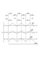
図3は、蓄電システム210の動作の一例を概略的に示す。図3は、制御信号φ22および制御信号φ24の波形の一例に対応づけて、グラフ302、グラフ304およびグラフ306を示す。グラフ302、グラフ304およびグラフ306において、横軸は時間の経過を示す。また、縦軸はインダクタ電流ILの大きさを示す。図3において、インダクタ電流ILの大きさは、接続点263から接続点243に向かって流れる電流(図2において実線の矢印で示す。)を正として表す。
FIG. 3 schematically shows an example of the operation of the power storage system 210. FIG. 3 shows a graph 302, a graph 304, and a graph 306 in association with examples of the waveforms of the control signal φ22 and the control signal φ24. In the graph 302, the graph 304, and the graph 306, the horizontal axis indicates the passage of time. The vertical axis shows the magnitude of the inductor current I L. 3, the magnitude of the inductor current I L represents the current flowing from the connection point 263 toward the connecting point 243 (. Indicated by the solid line arrow in FIG. 2) as a positive.
グラフ302は、蓄電セル222の電圧E2が蓄電セル224の電圧E4よりも大きい場合のインダクタ電流ILの経時変化の一例を概略的に示す。グラフ304は、蓄電セル222の電圧E2が蓄電セル224の電圧E4よりも小さい場合のインダクタ電流ILの経時変化の一例を概略的に示す。グラフ306は、蓄電セル222の電圧E2と蓄電セル224の電圧E4とが略同一である場合のインダクタ電流ILの経時変化の一例を概略的に示す。
Graph 302 illustrates an example of a temporal change of the inductor current I L when the voltage E 2 of the energy storage cell 222 is greater than the voltage E 4 of the electric storage cell 224 schematically. Graph 304 illustrates an example of a temporal change of the inductor current I L when the voltage E 2 of the energy storage cell 222 is smaller than the voltage E 4 of the electric storage cell 224 schematically. Graph 306 illustrates an example of a temporal change of the inductor current I L when the voltage E 2 of the energy storage cell 222 and the voltage E 4 storage cells 224 are substantially the same schematically.
図3において、制御信号φ22および制御信号φ24は、デューティ比が50%の方形波である。図3に示すように、制御信号φ22および制御信号φ24は、スイッチング素子252およびスイッチング素子254の一方がオン状態の間は他方がオフ状態になるように、互いに相補な論理または位相極性を有する。
In FIG. 3, the control signal φ22 and the control signal φ24 are square waves having a duty ratio of 50%. As shown in FIG. 3, control signal φ22 and control signal φ24 have complementary logic or phase polarities so that one of switching element 252 and switching element 254 is in the off state while the other is in the on state.
グラフ302に示すように、蓄電セル222の電圧E2が蓄電セル224の電圧E4よりも大きい場合には、スイッチング素子252がオン状態のときに、蓄電セル222の正極側-スイッチング素子252-接続点263-ヒューズ290-インダクタ250-接続点243-蓄電セル222の負極側の電流経路で電流が流れる。このとき、インダクタ250には、インダクタ電流ILが図2における実線矢印の方向に充電される。
As shown in the graph 302, when the voltage E 2 of the energy storage cell 222 is greater than the voltage E 4 of the electric storage cell 224, when the switching element 252 is ON, the positive electrode side of the storage cells 222 - switching element 25 2 A current flows in a current path on the negative side of the connection point 263 -the fuse 290 -the inductor 250 -the connection point 243 -the storage cell 222. At this time, the inductor 250, the inductor current I L is charged in the direction of the solid arrow in FIG.
次に、スイッチング素子252がオフ状態になり、スイッチング素子254がオン状態になると、インダクタ250に充電されたインダクタ電流ILがインダクタ250の一端-接続点243-蓄電セル224-スイッチング素子254-接続点263-ヒューズ290-インダクタ250の他端の電流経路で放電される。この放電は、蓄電セル224を充電しながら行われる。図3に示すように、インダクタ電流ILは放電により時間と共に減少し、放電電流が0になると、インダクタ250には、放電電流とは逆方向の充電電流が流れるようになる。
Next, the switching element 252 is turned off, the switching element 254 is turned on, the inductor current I L is charged in the inductor 250 of the inductor 250 at one end - the connection point 243- storage cell 224-switching element 254- connection It is discharged in the current path at point 263-fuse 290-inductor 250 at the other end. This discharge is performed while charging the storage cell 224. As shown in FIG. 3, the inductor current I L decreases with time due to the discharge, the discharge current becomes zero, the inductor 250, to flow the opposite direction of the charge current and the discharge current.
ここで、スイッチング素子252および制御信号発生部272の少なくとも一方の故障により、スイッチング素子252が閉じたままになると、接続点243と接続点263との間に過電流が流れる場合がある。しかし、本実施形態によれば、接続点243と接続点263との間に流れる電流の大きさが予め定められた値を超えると、ヒューズ290が溶断して、インダクタ250に流れる電流を制限する。これにより、蓄電セル222を保護することができる。
Here, if at least one of the switching element 252 and the control signal generation unit 272 fails and the switching element 252 remains closed, an overcurrent may flow between the connection point 243 and the connection point 263. However, according to the present embodiment, when the magnitude of the current flowing between the connection point 243 and the connection point 263 exceeds a predetermined value, the fuse 290 is blown and the current flowing through the inductor 250 is limited. . Thereby, the electrical storage cell 222 can be protected.
グラフ304に示すように、蓄電セル222の電圧E2が蓄電セル224の電圧E4よりも小さい場合には、スイッチング素子254がオン状態のときに、蓄電セル224の正極側-接続点243-インダクタ250-ヒューズ290-接続点263-スイッチング素子254-蓄電セル224の負極側の電流経路で電流が流れる。このとき、インダクタ250には、インダクタ電流ILが図2における点線矢印の方向に充電される。
As shown in the graph 304, when the voltage E 2 of the energy storage cell 222 is smaller than the voltage E 4 of the electric storage cell 224, when the switching element 254 is ON, the positive electrode side of the storage cells 224 - connection point 243- Inductor 250-fuse 290-connection point 263-switching element 254-current flows through the current path on the negative electrode side of power storage cell 224. At this time, the inductor 250, the inductor current I L is charged in the direction of the dotted arrow in FIG.
次に、スイッチング素子254がオフ状態になり、スイッチング素子252がオン状態になると、インダクタ250に充電されたインダクタ電流ILがインダクタ250の他端-ヒューズ290-接続点263-スイッチング素子252-蓄電セル222-接続点243-インダクタ250の一端の電流経路で放電される。この放電は、蓄電セル222を充電しながら行われる。
Next, the switching element 254 is turned off, the switching element 252 is turned on, the other end of the inductor current I L inductor 250 charged in the inductor 250 - Fuse 290- connection point 263- switching element 25 2 energy storage The cell 222 -the connection point 243 -discharged in the current path at one end of the inductor 250. This discharge is performed while charging the storage cell 222.
ここで、スイッチング素子254および制御信号発生部272の少なくとも一方の故障により、スイッチング素子254が閉じたままになると、接続点243と接続点263との間に過電流が流れる場合がある。しかし、本実施形態によれば、接続点243と接続点263との間に流れる電流の大きさが予め定められた値を超えると、ヒューズ290が溶断して、インダクタ250に流れる電流を制限する。これにより、蓄電セル224を保護することができる。
Here, if at least one of the switching element 254 and the control signal generation unit 272 fails and the switching element 254 remains closed, an overcurrent may flow between the connection point 243 and the connection point 263. However, according to the present embodiment, when the magnitude of the current flowing between the connection point 243 and the connection point 263 exceeds a predetermined value, the fuse 290 is blown and the current flowing through the inductor 250 is limited. . Thereby, the electrical storage cell 224 can be protected.
上記のように、バランス補正回路232が第1の開閉回路と、第2の開閉回路とに交互に電流を流すことで、蓄電セル122と蓄電セル124との間でインダクタ250を介して電気エネルギーを授受することができる。その結果、蓄電セル122および蓄電セル124の電圧を均等化させることができる。
As described above, the balance correction circuit 232 causes a current to flow alternately between the first switching circuit and the second switching circuit, whereby electric energy is passed between the storage cell 122 and the storage cell 124 via the inductor 250. Can be exchanged. As a result, the voltages of the storage cell 122 and the storage cell 124 can be equalized.
グラフ306に示すように、蓄電セル222の電圧E2と蓄電セル224の電圧E4とが略同一である場合には、スイッチング素子252またはスイッチング素子254がオン状態の期間において、インダクタ電流ILの放電と充電とがほぼ等量ずつ実施される。その結果、電圧がほぼバランスした状態を維持することができる。
As shown in the graph 306, when the voltage E 2 of the energy storage cell 222 and the voltage E 4 storage cells 224 are substantially the same, the switching element 252 or the switching element 254 in the period of the ON state, the inductor current I L The discharging and charging are performed in substantially equal amounts. As a result, it is possible to maintain a state where the voltages are almost balanced.
本実施形態においては、説明を簡単にする目的で、制御信号φ22および制御信号φ24のデューティ比が50%である場合について説明した。しかし、制御信号φ22および制御信号φ24はこれに限定されない。制御信号φ22および制御信号φ24のデューティ比は、蓄電セル222および蓄電セル224の電圧差に応じて変更されてよい。
In the present embodiment, the case where the duty ratio of the control signal φ22 and the control signal φ24 is 50% has been described for the purpose of simplifying the description. However, the control signal φ22 and the control signal φ24 are not limited to this. The duty ratio of control signal φ22 and control signal φ24 may be changed according to the voltage difference between power storage cell 222 and power storage cell 224.
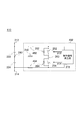
図4は、蓄電システム410の一例を概略的に示す。蓄電システム410は、端子212と、端子214と、直列に接続された蓄電セル222および蓄電セル224と、バランス補正回路432とを備える。バランス補正回路432は、バランス補正装置の一例であってよい。
FIG. 4 schematically shows an example of the power storage system 410. The power storage system 410 includes a terminal 212, a terminal 214, a power storage cell 222 and a power storage cell 224 connected in series, and a balance correction circuit 432. The balance correction circuit 432 may be an example of a balance correction device.
バランス補正回路432は、図2に関連して説明した第1の開閉回路および第2の開閉回路のそれぞれが電流制限素子を有する点でバランス補正回路232と相違する。その他の点については、バランス補正回路232と同様の構成を有してよい。バランス補正回路232の各部と同一または類似の部分には同一の参照番号を付して重複する説明を除く。また、蓄電システム110は、蓄電システム410と同様の構成を有してよい。バランス補正回路132、バランス補正回路134およびバランス補正回路136は、バランス補正回路432と同様の構成を有してよい。
The balance correction circuit 432 is different from the balance correction circuit 232 in that each of the first switching circuit and the second switching circuit described with reference to FIG. 2 has a current limiting element. Other points may have the same configuration as the balance correction circuit 232. Portions that are the same as or similar to the respective portions of the balance correction circuit 232 are denoted by the same reference numerals, and redundant description is omitted. In addition, the power storage system 110 may have a configuration similar to that of the power storage system 410. The balance correction circuit 132, the balance correction circuit 134, and the balance correction circuit 136 may have the same configuration as the balance correction circuit 432.
バランス補正回路432は、蓄電セル222および蓄電セル224の電圧を均等化させる。バランス補正回路432は、インダクタ250と、スイッチング素子252と、スイッチング素子254と、制御信号発生部272と、ダイオード282と、ダイオード284と、ヒューズ492と、ヒューズ494とを備える。ヒューズ492およびヒューズ494は、電流制限素子の一例であってよい。
The balance correction circuit 432 equalizes the voltages of the storage cell 222 and the storage cell 224. The balance correction circuit 432 includes an inductor 250, a switching element 252, a switching element 254, a control signal generation unit 272, a diode 282, a diode 284, a fuse 492, and a fuse 494. The fuse 492 and the fuse 494 may be an example of a current limiting element.
ヒューズ492は、蓄電セル222の正極側とスイッチング素子252との間に配されてよい。これにより、ヒューズ492は、スイッチング素子252がオン動作したときに、インダクタ250と直列に接続される。スイッチング素子252および制御信号発生部272の少なくとも一方の故障により、スイッチング素子252が閉じたままになると、蓄電セル222の正極側とスイッチング素子252との間に過電流が流れる場合がある。しかし、本実施形態によれば、蓄電セル222の正極側とスイッチング素子252との間に流れる電流の大きさが予め定められた値を超えると、ヒューズ492が溶断して、インダクタ250に流れる電流を制限する。これにより、蓄電セル222を保護することができる。
The fuse 492 may be disposed between the positive electrode side of the storage cell 222 and the switching element 252. Thereby, the fuse 492 is connected in series with the inductor 250 when the switching element 252 is turned on. If the switching element 252 remains closed due to a failure of at least one of the switching element 252 and the control signal generation unit 272, an overcurrent may flow between the positive electrode side of the storage cell 222 and the switching element 252. However, according to the present embodiment, when the magnitude of the current flowing between the positive electrode side of the storage cell 222 and the switching element 252 exceeds a predetermined value, the fuse 492 blows and the current flowing through the inductor 250 Limit. Thereby, the electrical storage cell 222 can be protected.
ヒューズ494は、蓄電セル224の負極側とスイッチング素子254との間に配されてよい。これにより、ヒューズ494は、スイッチング素子254がオン動作したときに、インダクタ250に直列に接続される。スイッチング素子254および制御信号発生部272の少なくとも一方の故障により、スイッチング素子254が閉じたままになると、蓄電セル224の負極側とスイッチング素子254との間に過電流が流れる場合がある。しかし、本実施形態によれば、蓄電セル224の負極側とスイッチング素子254との間に流れる電流の大きさが予め定められた値を超えると、ヒューズ494が溶断して、インダクタ250に流れる電流を制限する。これにより、蓄電セル224を保護することができる。
The fuse 494 may be disposed between the negative electrode side of the storage cell 224 and the switching element 254. Thereby, the fuse 494 is connected in series to the inductor 250 when the switching element 254 is turned on. If the switching element 254 remains closed due to a failure of at least one of the switching element 254 and the control signal generator 272, an overcurrent may flow between the negative electrode side of the storage cell 224 and the switching element 254. However, according to the present embodiment, when the magnitude of the current flowing between the negative electrode side of the storage cell 224 and the switching element 254 exceeds a predetermined value, the fuse 494 is blown, and the current flowing through the inductor 250 Limit. Thereby, the electrical storage cell 224 can be protected.
ヒューズ492およびヒューズ494の少なくとも一方は、過電流遮断型ヒューズまたは温度ヒューズであってよい。本実施形態において、電流制限素子としてヒューズを用いる場合について説明した。しかし、電流制限素子はこれに限定されない。電流制限素子は、温度上昇により内部抵抗が増大するPTCサーミスタであってもよい。電流制限素子は、電流遮断機であってもよい。
At least one of the fuse 492 and the fuse 494 may be an overcurrent interruption type fuse or a thermal fuse. In the present embodiment, the case where a fuse is used as the current limiting element has been described. However, the current limiting element is not limited to this. The current limiting element may be a PTC thermistor whose internal resistance increases as the temperature rises. The current limiting element may be a current breaker.
本実施形態において、ヒューズ492が、蓄電セル222の正極側とスイッチング素子252との間に配される場合について説明した。しかし、ヒューズ492の個数または設置場所はこれに限定されない。ヒューズ492は、インダクタ250の他端とスイッチング素子252との間に配されてもよい。これにより、ヒューズ492は、スイッチング素子252がオン動作したときに、インダクタ250と直列に接続される。
In the present embodiment, the case where the fuse 492 is disposed between the positive electrode side of the storage cell 222 and the switching element 252 has been described. However, the number or installation location of the fuses 492 is not limited to this. The fuse 492 may be disposed between the other end of the inductor 250 and the switching element 252. Thereby, the fuse 492 is connected in series with the inductor 250 when the switching element 252 is turned on.
本実施形態において、ヒューズ494が、蓄電セル224の負極側とスイッチング素子254との間に配される場合について説明した。しかし、ヒューズ494の個数または設置場所はこれに限定されない。ヒューズ494は、インダクタ250の他端とスイッチング素子254との間に配されてもよい。これにより、ヒューズ494は、スイッチング素子254がオン動作したときに、インダクタ250と直列に接続される。
In the present embodiment, the case where the fuse 494 is disposed between the negative electrode side of the storage cell 224 and the switching element 254 has been described. However, the number or installation location of the fuses 494 is not limited to this. The fuse 494 may be disposed between the other end of the inductor 250 and the switching element 254. Thereby, the fuse 494 is connected in series with the inductor 250 when the switching element 254 is turned on.
以上、本発明を実施の形態を用いて説明したが、本発明の技術的範囲は上記実施の形態に記載の範囲には限定されない。上記実施の形態に、多様な変更または改良を加えることが可能であることが当業者に明らかである。その様な変更または改良を加えた形態も本発明の技術的範囲に含まれ得ることが、請求の範囲の記載から明らかである。
As mentioned above, although this invention was demonstrated using embodiment, the technical scope of this invention is not limited to the range as described in the said embodiment. It will be apparent to those skilled in the art that various modifications or improvements can be added to the above-described embodiment. It is apparent from the scope of the claims that the embodiments added with such changes or improvements can be included in the technical scope of the present invention.
請求の範囲、明細書、および図面中において示した装置、システム、プログラム、および方法における動作、手順、ステップ、および段階等の各処理の実行順序は、特段「より前に」、「先立って」等と明示しておらず、また、前の処理の出力を後の処理で用いるのでない限り、任意の順序で実現しうることに留意すべきである。請求の範囲、明細書、および図面中の動作フローに関して、便宜上「まず、」、「次に、」等を用いて説明したとしても、この順で実施することが必須であることを意味するものではない。
The execution order of each process such as operations, procedures, steps, and stages in the apparatus, system, program, and method shown in the claims, the description, and the drawings is particularly “before” or “prior”. It should be noted that they can be implemented in any order unless the output of the previous process is used in the subsequent process. Regarding the operation flow in the claims, the description, and the drawings, even if it is described using “first”, “next”, etc. for the sake of convenience, it means that it is essential to carry out in this order. is not.
100 装置、102 モータ、110 蓄電システム、112 端子、114 端子、122 蓄電セル、124 蓄電セル、126 蓄電セル、128 蓄電セル、132 バランス補正回路、134 バランス補正回路、136 バランス補正回路、143 接続点、145 接続点、147 接続点、210 蓄電システム、212 端子、214 端子、222 蓄電セル、224 蓄電セル、232 バランス補正回路、243 接続点、250 インダクタ、252 スイッチング素子、254 スイッチング素子、263 接続点、272 制御信号発生部、282 ダイオード、284 ダイオード、290 ヒューズ、302 グラフ、304 グラフ、306 グラフ、410 蓄電システム、432 バランス補正回路、492 ヒューズ、494 ヒューズ
100 device, 102 motor, 110 power storage system, 112 terminal, 114 terminal, 122 power storage cell, 124 power storage cell, 126 power storage cell, 128 power storage cell, 132 balance correction circuit, 134 balance correction circuit, 136 balance correction circuit, 143 connection point 145 connection point, 147 connection point, 210 storage system, 212 terminal, 214 terminal, 222 storage cell, 224 storage cell, 232 balance correction circuit, 243 connection point, 250 inductor, 252 switching element, 254 switching element, 263 connection point 272 control signal generator, 282 diode, 284 diode, 290 fuse, 302 graph, 304 graph, 306 graph, 410 power storage system, 432 balance compensation Circuit, 492 fuses, 494 fuse
Claims (6)
- 直列に接続された第1の蓄電セルおよび第2の蓄電セルの電圧を均等化させるバランス補正装置であって、
前記第1の蓄電セルの一端と前記第2の蓄電セルの一端との接続点に、一端が電気的に接続されるインダクタと、
前記インダクタの他端と前記第1の蓄電セルの他端との間に電気的に接続される第1のスイッチング素子と、
前記インダクタの他端と前記第2の蓄電セルの他端との間に電気的に接続される第2のスイッチング素子と、
前記インダクタに直列に接続され、前記インダクタに流れる電流の大きさが予め定められた値を超えると、前記インダクタに流れる電流を制限する電流制限素子と、
を備える、バランス補正装置。 A balance correction device for equalizing the voltages of a first storage cell and a second storage cell connected in series,
An inductor having one end electrically connected to a connection point between one end of the first storage cell and one end of the second storage cell;
A first switching element electrically connected between the other end of the inductor and the other end of the first storage cell;
A second switching element electrically connected between the other end of the inductor and the other end of the second storage cell;
A current limiting element connected in series to the inductor and limiting a current flowing through the inductor when a magnitude of a current flowing through the inductor exceeds a predetermined value;
A balance correction device. - 前記電流制限素子が、前記第1の蓄電セルの一端および前記第2の蓄電セルの一端の接続点と、前記第1のスイッチング素子および前記第2のスイッチング素子の接続点との間に、前記インダクタに直列に接続される、
請求項1に記載のバランス補正装置。 The current limiting element is connected between a connection point of one end of the first power storage cell and one end of the second power storage cell, and a connection point of the first switching element and the second switching element. Connected in series to the inductor,
The balance correction apparatus according to claim 1. - 前記電流制限素子が、
前記第1の蓄電セルの他端と、前記第1のスイッチング素子との間に、前記インダクタに直列に接続される第1の電流制限素子と、
前記第2の蓄電セルの他端と、前記第2のスイッチング素子との間に、前記インダクタに直列に接続される第2の電流制限素子と、
を有する、
請求項1または請求項2に記載のバランス補正装置。 The current limiting element is
A first current limiting element connected in series with the inductor between the other end of the first storage cell and the first switching element;
A second current limiting element connected in series with the inductor between the other end of the second storage cell and the second switching element;
Having
The balance correction apparatus according to claim 1 or 2. - 前記電流制限素子が、ヒューズである、
請求項1から請求項3までの何れか一項に記載のバランス補正装置。 The current limiting element is a fuse;
The balance correction apparatus as described in any one of Claim 1- Claim 3. - 前記ヒューズが、過電流遮断型ヒューズまたは温度ヒューズである、
請求項4に記載のバランス補正装置。 The fuse is an overcurrent interruption type fuse or a thermal fuse;
The balance correction apparatus according to claim 4. - 直列に接続された第1の蓄電セルおよび第2の蓄電セルと、
前記第1の蓄電セルおよび前記第2の蓄電セルの電圧を均等化させる、請求項1から請求項5までの何れか一項に記載のバランス補正装置と、
を備える、蓄電システム。 A first storage cell and a second storage cell connected in series;
The balance correction device according to any one of claims 1 to 5, wherein the voltages of the first power storage cell and the second power storage cell are equalized.
A power storage system comprising:
Priority Applications (3)
| Application Number | Priority Date | Filing Date | Title |
|---|---|---|---|
| EP12755163.8A EP2685592A4 (en) | 2011-03-08 | 2012-03-06 | Balance correction device and electricity storage system |
| CN2012800115790A CN103430420A (en) | 2011-03-08 | 2012-03-06 | Balance correction device and electricity storage system |
| US14/013,047 US20140009116A1 (en) | 2011-03-08 | 2013-08-29 | Balance correction apparatus and electric storage system |
Applications Claiming Priority (2)
| Application Number | Priority Date | Filing Date | Title |
|---|---|---|---|
| JP2011050662A JP2012191679A (en) | 2011-03-08 | 2011-03-08 | Balance correction apparatus and power storage system |
| JP2011-050662 | 2011-03-08 |
Related Child Applications (1)
| Application Number | Title | Priority Date | Filing Date |
|---|---|---|---|
| US14/013,047 Continuation US20140009116A1 (en) | 2011-03-08 | 2013-08-29 | Balance correction apparatus and electric storage system |
Publications (1)
| Publication Number | Publication Date |
|---|---|
| WO2012120878A1 true WO2012120878A1 (en) | 2012-09-13 |
Family
ID=46797849
Family Applications (1)
| Application Number | Title | Priority Date | Filing Date |
|---|---|---|---|
| PCT/JP2012/001537 WO2012120878A1 (en) | 2011-03-08 | 2012-03-06 | Balance correction device and electricity storage system |
Country Status (5)
| Country | Link |
|---|---|
| US (1) | US20140009116A1 (en) |
| EP (1) | EP2685592A4 (en) |
| JP (1) | JP2012191679A (en) |
| CN (1) | CN103430420A (en) |
| WO (1) | WO2012120878A1 (en) |
Families Citing this family (17)
| Publication number | Priority date | Publication date | Assignee | Title |
|---|---|---|---|---|
| CN104170205B (en) | 2012-03-19 | 2018-03-16 | 艾达司股份有限公司 | Balance correction device and power storage system |
| JP5864320B2 (en) | 2012-03-19 | 2016-02-17 | Evtd株式会社 | Balance correction device and power storage system |
| JP2015019441A (en) * | 2013-07-09 | 2015-01-29 | Fdk株式会社 | Balance correction device and power storage device |
| CN104852411A (en) * | 2014-02-18 | 2015-08-19 | 宝星电器(上海)有限公司 | Cascade storage battery charge/discharge balancing system |
| US20160049883A1 (en) * | 2014-08-14 | 2016-02-18 | Google Inc. | Power-Balancing Circuits for Stacked Topologies |
| KR101592227B1 (en) | 2014-09-30 | 2016-02-05 | 한국전력공사 | Circuit for controlling dc bus imbalance of energy storage system |
| CN105703434A (en) * | 2016-03-21 | 2016-06-22 | 南京金龙新能源汽车研究院有限公司 | Battery management system with active equalization function |
| CN106059008B (en) * | 2016-07-26 | 2018-10-26 | 圣邦微电子(北京)股份有限公司 | A kind of battery-efficient transfer equalizing circuit |
| JP6814437B2 (en) * | 2017-02-13 | 2021-01-20 | NExT−e Solutions株式会社 | Control device, balance correction device, power storage system, and device |
| CN107276168A (en) * | 2017-07-05 | 2017-10-20 | 东莞中汽宏远汽车有限公司 | Active equalization method and computer-readable medium for battery pack |
| CN107276167A (en) * | 2017-07-05 | 2017-10-20 | 东莞中汽宏远汽车有限公司 | Method for carrying out active equalization to battery pack using multilayer equalizing circuit |
| CN107195994A (en) * | 2017-07-07 | 2017-09-22 | 东莞中汽宏远汽车有限公司 | Active equalization device for battery pack |
| CN107240946A (en) * | 2017-07-07 | 2017-10-10 | 东莞中汽宏远汽车有限公司 | Active equalization device for battery pack |
| CN107195993A (en) * | 2017-07-07 | 2017-09-22 | 东莞中汽宏远汽车有限公司 | Active equalization device for battery pack |
| JP6928347B2 (en) * | 2017-08-02 | 2021-09-01 | NExT−e Solutions株式会社 | Management device, power storage device, power storage system, and electrical equipment |
| JP7007681B2 (en) * | 2017-09-29 | 2022-01-25 | NExT-e Solutions株式会社 | Control device, balance correction system, power storage system, and device |
| US11342776B2 (en) * | 2020-06-15 | 2022-05-24 | Magnetic Energy Charging, Inc. | Battery charger and method for charging a battery |
Citations (5)
| Publication number | Priority date | Publication date | Assignee | Title |
|---|---|---|---|---|
| JP2002010501A (en) * | 2000-06-23 | 2002-01-11 | Honda Motor Co Ltd | Capacity equalizing apparatus for capacitor |
| JP2007280757A (en) * | 2006-04-06 | 2007-10-25 | Matsushita Electric Ind Co Ltd | Battery pack and electric apparatus using same |
| JP2008017605A (en) * | 2006-07-05 | 2008-01-24 | Fdk Corp | Voltage balancing correction circuit of series cell |
| JP2008206396A (en) * | 2004-08-27 | 2008-09-04 | Fdk Corp | Balance correcting device for secondary batteries connected in series, and its correcting method |
| JP2009232660A (en) * | 2008-03-25 | 2009-10-08 | Fdk Corp | Voltage balance correction circuit of series cell |
Family Cites Families (8)
| Publication number | Priority date | Publication date | Assignee | Title |
|---|---|---|---|---|
| US5742150A (en) * | 1996-09-16 | 1998-04-21 | Khuwatsamrit; Thakoengdet | Power supply and method of protecting batteries therein |
| US6259229B1 (en) * | 1998-04-30 | 2001-07-10 | Daimlerchrysler Corporation | Circulating current battery heater |
| US5982142A (en) * | 1998-05-22 | 1999-11-09 | Vanner, Inc. | Storage battery equalizer with improved, constant current output filter, overload protection, temperature compensation and error signal feedback |
| US7061207B2 (en) * | 2002-08-09 | 2006-06-13 | H2Eye (International ) Limited | Cell equalizing circuit |
| US6873134B2 (en) * | 2003-07-21 | 2005-03-29 | The Boeing Company | Autonomous battery cell balancing system with integrated voltage monitoring |
| JP2005143160A (en) * | 2003-11-04 | 2005-06-02 | Toshiba Corp | Secondary battery pack and secondary battery system |
| CN100358212C (en) * | 2005-04-05 | 2007-12-26 | 苏州星恒电源有限公司 | Battery equalization method and battery equalization circuit |
| JP5387703B2 (en) * | 2012-01-25 | 2014-01-15 | 株式会社豊田自動織機 | Battery cell voltage equalization circuit |
-
2011
- 2011-03-08 JP JP2011050662A patent/JP2012191679A/en active Pending
-
2012
- 2012-03-06 CN CN2012800115790A patent/CN103430420A/en active Pending
- 2012-03-06 EP EP12755163.8A patent/EP2685592A4/en not_active Withdrawn
- 2012-03-06 WO PCT/JP2012/001537 patent/WO2012120878A1/en active Application Filing
-
2013
- 2013-08-29 US US14/013,047 patent/US20140009116A1/en not_active Abandoned
Patent Citations (5)
| Publication number | Priority date | Publication date | Assignee | Title |
|---|---|---|---|---|
| JP2002010501A (en) * | 2000-06-23 | 2002-01-11 | Honda Motor Co Ltd | Capacity equalizing apparatus for capacitor |
| JP2008206396A (en) * | 2004-08-27 | 2008-09-04 | Fdk Corp | Balance correcting device for secondary batteries connected in series, and its correcting method |
| JP2007280757A (en) * | 2006-04-06 | 2007-10-25 | Matsushita Electric Ind Co Ltd | Battery pack and electric apparatus using same |
| JP2008017605A (en) * | 2006-07-05 | 2008-01-24 | Fdk Corp | Voltage balancing correction circuit of series cell |
| JP2009232660A (en) * | 2008-03-25 | 2009-10-08 | Fdk Corp | Voltage balance correction circuit of series cell |
Non-Patent Citations (1)
| Title |
|---|
| See also references of EP2685592A4 * |
Also Published As
| Publication number | Publication date |
|---|---|
| EP2685592A4 (en) | 2014-10-01 |
| EP2685592A1 (en) | 2014-01-15 |
| CN103430420A (en) | 2013-12-04 |
| US20140009116A1 (en) | 2014-01-09 |
| JP2012191679A (en) | 2012-10-04 |
Similar Documents
| Publication | Publication Date | Title |
|---|---|---|
| WO2012120878A1 (en) | Balance correction device and electricity storage system | |
| JP5864320B2 (en) | Balance correction device and power storage system | |
| WO2017086349A1 (en) | Control device, power storage device, and power storage system | |
| CN107968446B (en) | Distributed battery pack power supply system and charge-discharge control method | |
| US20200055412A1 (en) | Circuit and charging method for an electrical energy storage system | |
| JP6928347B2 (en) | Management device, power storage device, power storage system, and electrical equipment | |
| JP6178328B2 (en) | DC voltage source including an electrochemical cell | |
| JP5744598B2 (en) | Balance correction device and power storage system | |
| JP5827019B2 (en) | Balance correction device and power storage system | |
| US20130119934A1 (en) | Secondary battery pack connection control method, power storage system, and secondary battery pack | |
| JP2013005677A (en) | Cell balancer | |
| WO2013157576A1 (en) | Battery balancing system and method | |
| JP2020503834A (en) | Improved circuit for bidirectional lossless balancing of series battery packs based on inductive energy storage | |
| JP2014239559A (en) | Power storage system | |
| JP5645950B2 (en) | Method for equalizing the voltage of an electrical storage unit | |
| JP5718702B2 (en) | Balance correction device and power storage system | |
| JP5650235B2 (en) | Method for equalizing the voltage of an electrical storage unit | |
| WO2013005804A1 (en) | Switching device | |
| WO2015005273A1 (en) | Balance correction device and electricity storage device | |
| JP5077489B2 (en) | Power storage device and railway vehicle | |
| TW202308259A (en) | Battery cell balance circuit and method of operating the same | |
| JP2012191820A (en) | Power supply system | |
| WO2013132731A1 (en) | Electricity storage device and method for controlling electricity storage device | |
| TW201332251A (en) | Rechargeable battery management system and method thereof |
Legal Events
| Date | Code | Title | Description |
|---|---|---|---|
| 121 | Ep: the epo has been informed by wipo that ep was designated in this application |
Ref document number: 12755163 Country of ref document: EP Kind code of ref document: A1 |
|
| WWE | Wipo information: entry into national phase |
Ref document number: 2012755163 Country of ref document: EP |
|
| NENP | Non-entry into the national phase |
Ref country code: DE |