WO2012118200A1 - 金属薄膜の製膜方法、金属薄膜、および金属薄膜の製膜装置 - Google Patents
金属薄膜の製膜方法、金属薄膜、および金属薄膜の製膜装置 Download PDFInfo
- Publication number
- WO2012118200A1 WO2012118200A1 PCT/JP2012/055448 JP2012055448W WO2012118200A1 WO 2012118200 A1 WO2012118200 A1 WO 2012118200A1 JP 2012055448 W JP2012055448 W JP 2012055448W WO 2012118200 A1 WO2012118200 A1 WO 2012118200A1
- Authority
- WO
- WIPO (PCT)
- Prior art keywords
- thin film
- raw material
- metal thin
- reactive gas
- organometallic compound
- Prior art date
- Legal status (The legal status is an assumption and is not a legal conclusion. Google has not performed a legal analysis and makes no representation as to the accuracy of the status listed.)
- Ceased
Links
- 0 CC1=C(*)C(*)=C(C*(C(*)(C=C(C)C(*)=C2*)C2=*)I)[C@]1* Chemical compound CC1=C(*)C(*)=C(C*(C(*)(C=C(C)C(*)=C2*)C2=*)I)[C@]1* 0.000 description 2
Images
Classifications
-
- C—CHEMISTRY; METALLURGY
- C23—COATING METALLIC MATERIAL; COATING MATERIAL WITH METALLIC MATERIAL; CHEMICAL SURFACE TREATMENT; DIFFUSION TREATMENT OF METALLIC MATERIAL; COATING BY VACUUM EVAPORATION, BY SPUTTERING, BY ION IMPLANTATION OR BY CHEMICAL VAPOUR DEPOSITION, IN GENERAL; INHIBITING CORROSION OF METALLIC MATERIAL OR INCRUSTATION IN GENERAL
- C23C—COATING METALLIC MATERIAL; COATING MATERIAL WITH METALLIC MATERIAL; SURFACE TREATMENT OF METALLIC MATERIAL BY DIFFUSION INTO THE SURFACE, BY CHEMICAL CONVERSION OR SUBSTITUTION; COATING BY VACUUM EVAPORATION, BY SPUTTERING, BY ION IMPLANTATION OR BY CHEMICAL VAPOUR DEPOSITION, IN GENERAL
- C23C16/00—Chemical coating by decomposition of gaseous compounds, without leaving reaction products of surface material in the coating, i.e. chemical vapour deposition [CVD] processes
- C23C16/06—Chemical coating by decomposition of gaseous compounds, without leaving reaction products of surface material in the coating, i.e. chemical vapour deposition [CVD] processes characterised by the deposition of metallic material
- C23C16/18—Chemical coating by decomposition of gaseous compounds, without leaving reaction products of surface material in the coating, i.e. chemical vapour deposition [CVD] processes characterised by the deposition of metallic material from metallo-organic compounds
-
- C—CHEMISTRY; METALLURGY
- C23—COATING METALLIC MATERIAL; COATING MATERIAL WITH METALLIC MATERIAL; CHEMICAL SURFACE TREATMENT; DIFFUSION TREATMENT OF METALLIC MATERIAL; COATING BY VACUUM EVAPORATION, BY SPUTTERING, BY ION IMPLANTATION OR BY CHEMICAL VAPOUR DEPOSITION, IN GENERAL; INHIBITING CORROSION OF METALLIC MATERIAL OR INCRUSTATION IN GENERAL
- C23C—COATING METALLIC MATERIAL; COATING MATERIAL WITH METALLIC MATERIAL; SURFACE TREATMENT OF METALLIC MATERIAL BY DIFFUSION INTO THE SURFACE, BY CHEMICAL CONVERSION OR SUBSTITUTION; COATING BY VACUUM EVAPORATION, BY SPUTTERING, BY ION IMPLANTATION OR BY CHEMICAL VAPOUR DEPOSITION, IN GENERAL
- C23C16/00—Chemical coating by decomposition of gaseous compounds, without leaving reaction products of surface material in the coating, i.e. chemical vapour deposition [CVD] processes
- C23C16/44—Chemical coating by decomposition of gaseous compounds, without leaving reaction products of surface material in the coating, i.e. chemical vapour deposition [CVD] processes characterised by the method of coating
- C23C16/448—Chemical coating by decomposition of gaseous compounds, without leaving reaction products of surface material in the coating, i.e. chemical vapour deposition [CVD] processes characterised by the method of coating characterised by the method used for generating reactive gas streams, e.g. by evaporation or sublimation of precursor materials
- C23C16/4488—Chemical coating by decomposition of gaseous compounds, without leaving reaction products of surface material in the coating, i.e. chemical vapour deposition [CVD] processes characterised by the method of coating characterised by the method used for generating reactive gas streams, e.g. by evaporation or sublimation of precursor materials by in situ generation of reactive gas by chemical or electrochemical reaction
-
- C—CHEMISTRY; METALLURGY
- C23—COATING METALLIC MATERIAL; COATING MATERIAL WITH METALLIC MATERIAL; CHEMICAL SURFACE TREATMENT; DIFFUSION TREATMENT OF METALLIC MATERIAL; COATING BY VACUUM EVAPORATION, BY SPUTTERING, BY ION IMPLANTATION OR BY CHEMICAL VAPOUR DEPOSITION, IN GENERAL; INHIBITING CORROSION OF METALLIC MATERIAL OR INCRUSTATION IN GENERAL
- C23C—COATING METALLIC MATERIAL; COATING MATERIAL WITH METALLIC MATERIAL; SURFACE TREATMENT OF METALLIC MATERIAL BY DIFFUSION INTO THE SURFACE, BY CHEMICAL CONVERSION OR SUBSTITUTION; COATING BY VACUUM EVAPORATION, BY SPUTTERING, BY ION IMPLANTATION OR BY CHEMICAL VAPOUR DEPOSITION, IN GENERAL
- C23C16/00—Chemical coating by decomposition of gaseous compounds, without leaving reaction products of surface material in the coating, i.e. chemical vapour deposition [CVD] processes
- C23C16/44—Chemical coating by decomposition of gaseous compounds, without leaving reaction products of surface material in the coating, i.e. chemical vapour deposition [CVD] processes characterised by the method of coating
- C23C16/455—Chemical coating by decomposition of gaseous compounds, without leaving reaction products of surface material in the coating, i.e. chemical vapour deposition [CVD] processes characterised by the method of coating characterised by the method used for introducing gases into reaction chamber or for modifying gas flows in reaction chamber
- C23C16/45523—Pulsed gas flow or change of composition over time
-
- H—ELECTRICITY
- H10—SEMICONDUCTOR DEVICES; ELECTRIC SOLID-STATE DEVICES NOT OTHERWISE PROVIDED FOR
- H10P—GENERIC PROCESSES OR APPARATUS FOR THE MANUFACTURE OR TREATMENT OF DEVICES COVERED BY CLASS H10
- H10P14/00—Formation of materials, e.g. in the shape of layers or pillars
- H10P14/40—Formation of materials, e.g. in the shape of layers or pillars of conductive or resistive materials
- H10P14/42—Formation of materials, e.g. in the shape of layers or pillars of conductive or resistive materials using a gas or vapour
- H10P14/43—Chemical deposition, e.g. chemical vapour deposition [CVD]
Definitions
- the present invention relates to a method for forming a metal thin film, a metal thin film, and a metal thin film forming apparatus.
- transition elements are often used as the material for such a metal thin film, and techniques such as PVD (Physical Vapor Deposition) and CVD (Chemical Vapor Deposition) are known as film forming methods.
- PVD Physical Vapor Deposition
- CVD Chemical Vapor Deposition
- the PVD method is a film forming method called a physical vapor deposition method, and is characterized in that a thin film is formed by evaporating a substance by physical means, and sputtering and vapor deposition are classified into this method.
- the PVD method has the merit that a high-purity film can be produced.
- a vacuum higher than a high vacuum is required as a film forming condition, a large capital investment is required for the exhaust system, and a film is formed. There is a drawback that the step coverage of the film is poor.
- the CVD method is a film forming method called a chemical vapor deposition method, in which a metal raw material is supplied in a gaseous state onto a substrate, and a desired film is formed by dissociation / reaction by a chemical reaction on the gas phase or the substrate surface.
- a metal raw material is supplied in a gaseous state onto a substrate
- a desired film is formed by dissociation / reaction by a chemical reaction on the gas phase or the substrate surface.
- Methods classified into CVD methods include, for example, thermal CVD method, PECVD method (Plasma-Enhanced Chemical Vapor Deposition), HWCVD method (Hot Wire Chemical Vapor Deposition), ALD method (Atomic Layer film method). .
- the thermal CVD method is a method in which a metal raw material is transported in a gaseous state to the substrate surface, and a film is formed using thermal decomposition or surface reaction on the heated substrate. Although it depends on the type of surface reaction, it is generally excellent in step coverage because of its low sticking probability.
- the PECVD method is a method in which a metal raw material is appropriately decomposed in a gas phase using plasma energy and then transported to the substrate surface to form a film.
- a volatile raw material is used as the metal raw material, it is often possible to form a film.
- the HWCVD method is also called a Cat-CVD method, which is a method in which a metal raw material is dissociated by contacting a hot wire functioning as a catalyst, and transported to the substrate surface in that state to form a film.
- a catalyst a mesh-like metal may be used instead of a wire.
- the HWCVD method has not only the advantage that the exhaust system is inexpensive, but also the advantage that the area can be increased simply by stretching the wire.
- the ALD method is a film forming method also called an atomic layer deposition method, in which a metal raw material is transported until it is saturated and adsorbed on the substrate surface, and then a residual gas is exhausted and then a reaction gas is transported to the substrate surface to perform surface reaction.
- This is a method of forming a film by depositing one atomic layer or several atomic layers at a time.
- Patent Document 1 discloses a method of dissociating a metal raw material by bringing it into contact with a hot wire. (Hereinafter referred to as “HWARD method”).
- Non-Patent Document 1 discloses a technique for forming a metal thin film by thermal CVD under atmospheric pressure using biscyclopentadienyl cobalt (cobaltcene) as a metal raw material.
- the thermal CVD method often includes reaction by-products in the film, which makes it difficult to obtain a high-purity film and has a disadvantage that the resistance is higher than that of bulk metal.
- metal raw materials that can be used for thermal CVD film formation and film formation conditions are limited, and it is difficult to obtain a metal thin film with high purity and good step coverage.
- many of the metal raw materials used in the thermal CVD method contain oxygen and halogen, which has the disadvantage of adversely affecting the film quality of the metal thin film formed.
- the PECVD method also includes ionized reactive species in addition to the radical reactive species, and thus has a disadvantage that the adhesion rate is high and the step coverage is inferior to that of the thermal CVD method. In addition, there are inconveniences that the base is damaged by plasma and that impurities are more easily contained than in the thermal CVD method.
- the HWCVD method does not damage the underlayer, but if a metal raw material is used, a metal species is deposited on the wire or on the insulator portion of the wire, causing a short circuit. There was a disadvantage that it was not suitable for the membrane.
- the ALD method is basically the same as the thermal CVD method, there is a disadvantage that the metal raw materials and film forming conditions that can be used are limited.
- the method described in Patent Document 1 uses a tungsten material containing oxygen or halogen as the metal material, and there is a disadvantage that the metal material that can be used is limited.
- the metal raw material contains oxygen and halogen, there is a disadvantage that these adversely affect the film quality of the formed metal thin film.
- the thermal CVD method described in Non-Patent Document 1 is performed under atmospheric pressure, there is a disadvantage that the step coverage of the formed metal thin film is poor.
- the present invention employs the following configuration. (1) That is, in the first aspect of the present invention, a raw material transporting step for transporting an organometallic compound raw material onto a film forming object placed in a vacuum chamber, and a reactive gas is heated to a metal contact. And a reactive gas transporting step of transporting onto the film-forming object placed in the vacuum chamber after contacting the medium.
- the organometallic compound raw material and / or the reactive gas is selected from the group consisting of a carbon atom, a nitrogen atom, a hydrogen atom, a silicon atom, a phosphorus atom, a boron atom, and a metal atom. Preferably, it consists of only one or two or more atoms.
- the said organometallic compound raw material contains the organometallic compound shown by following Chemical formula (1) in the film forming method of said (1) and (2).
- M 1 is any one of cobalt, nickel, iron, manganese, ruthenium and chromium
- R 1 to R 5 are hydrogen or carbonized represented by C n H 2n + 1 where n is 1 or more. Hydrogen.
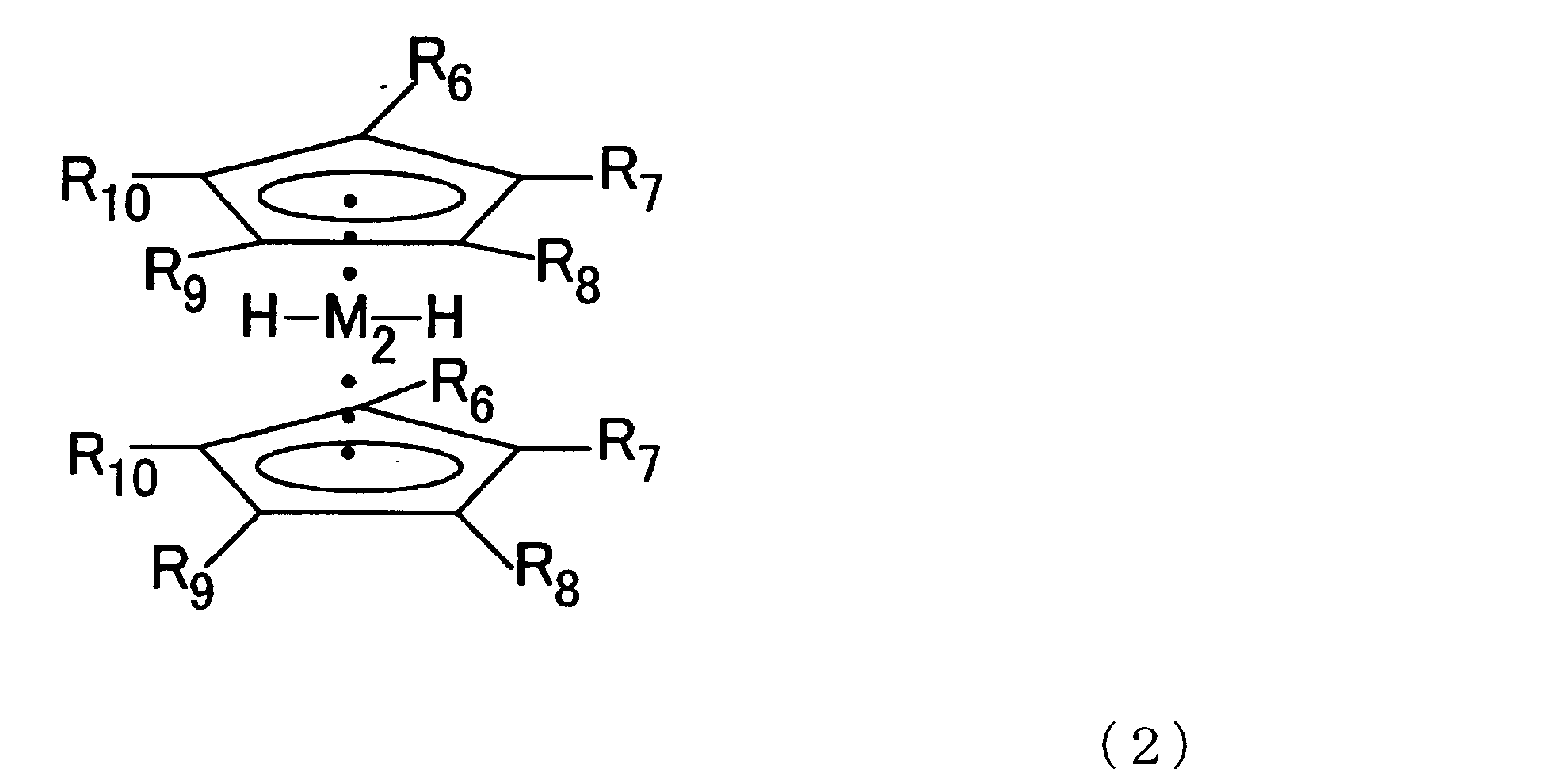
- the said organometallic compound raw material contains the organometallic compound shown by following Chemical formula (2) in the film forming method of said (1) and (2).
- M 2 is tungsten, molybdenum, or titanium
- R 6 to R 10 are hydrogen or a hydrocarbon represented by C n H 2n + 1 where n is 1 or more.
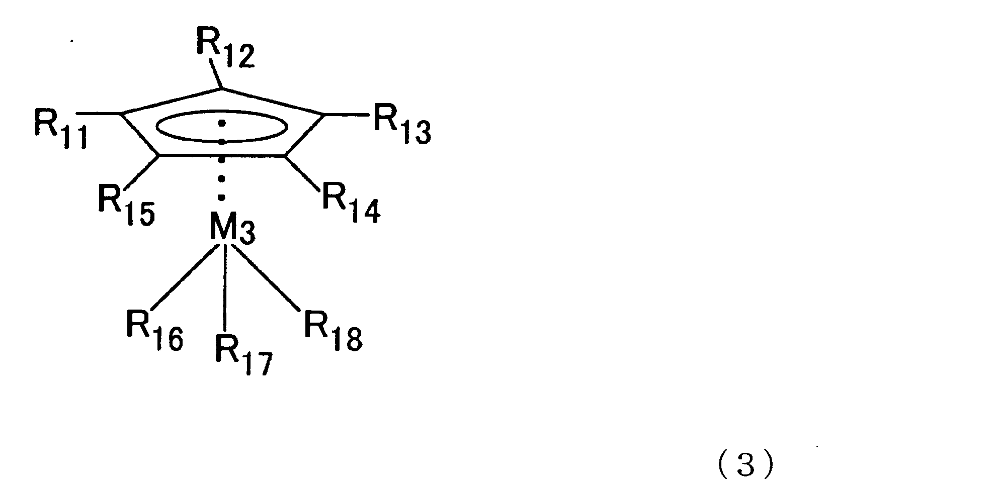
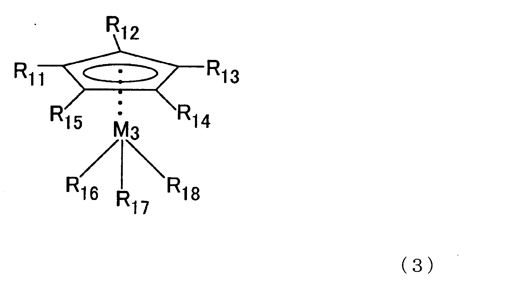
- the said organometallic compound raw material contains the organometallic compound shown by following Chemical formula (3) in the film forming method of said (1) and (2).
- M 3 is platinum, niobium, zirconium or titanium
- R 11 to R 15 are hydrogen or a hydrocarbon represented by C n H 2n + 1 where n is 1 or more
- R 16 to R 18 is a hydrocarbon represented by C n H 2n + 1 where n is 1 or more.
- the reactive gas contains at least one of ammonia, dimethylhydrazine, methylamine, dimethylamine, silane, disilane, and hydrogen. It is preferable.
- the metal catalyst body contains at least one of tungsten, platinum, rhodium and ruthenium.
- the metal catalyst body is heated by energization only during the reactive gas transfer step.
- the raw material transfer step and the reactive gas transfer step are alternately repeated, and the residual gas in the vacuum chamber is removed between the steps. It is preferable to have a purge step.
- the pressure in the vacuum chamber is 1.33 ⁇ 10 2 Pa or less in the reactive gas transfer step.
- a second aspect of the present invention is a metal thin film characterized by being formed by the method for forming a metal thin film according to any one of (1) to (11) above.
- a vacuum chamber in which a film forming object can be freely placed, and an organometallic compound raw material on the film forming object placed in the vacuum chamber.
- a raw material transporting means capable of transporting, and a reactive gas transporting means capable of transporting a reactive gas after contacting a heated metal catalyst body on a film-forming target placed in the vacuum chamber. It is a metal thin film forming apparatus characterized by having.
- n is an integer that can be arbitrarily selected and is preferably 1 to 15 It is more preferably 1 to 10, more preferably 1 to 5, and particularly preferably 1 to 3.
- C n H 2n + 1 include methyl, ethyl and butyl.
- R 1 to R 5 may be the same as or different from each other.
- R 6 to R 10 may be the same as or different from each other.
- R 11 to R 18 may be the same as or different from each other.
- all of R contained in the organometallic compound may be hydrogen, or all R, 1 to 8 or 2 to 4 R may be hydrocarbons arbitrarily selected.
- a metal thin film can be formed without using a high vacuum with low impurities and good step coverage.
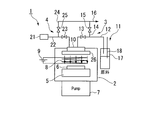
- FIG. 1 is a schematic configuration diagram showing a metal thin film forming apparatus according to an embodiment of the present invention.
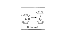
- FIG. 2A is a diagram showing the energy required for the release of cyclopentadienyl from cobaltene.
- FIG. 2B is a diagram showing the energy required for the release of cyclopentadienyl from cobaltocene in which H is bound to cobalt.
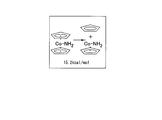
- FIG. 2C shows the energy required for the release of cyclopentadienyl from cobaltocene in which NH 2 is bonded to cobalt.
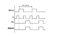
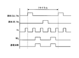
- FIG. 3 is a diagram showing a metal thin film deposition cycle in one embodiment of the present invention.
- FIG. 4 is a diagram showing a metal thin film deposition cycle in one embodiment of the present invention.
- the metal thin film deposition apparatus of the present embodiment is an apparatus capable of depositing a metal thin film by the HWALD method.
- a film forming apparatus 1 includes a vacuum chamber 2 that can be depressurized, a raw material transport unit 3 that can transport an organometallic compound raw material, and a reactive gas that can transport a reactive gas. And conveying means 4.
- a mounting table 5 is provided in the vacuum chamber 2, and the substrate 6 (film forming object) can be freely mounted on the mounting table 5.
- a heater (not shown) is provided inside the mounting table 5 so that the substrate 6 can be heated.
- the composition, shape, and size of the film-forming target may be arbitrarily selected unless there is a particular problem.
- an exhaust pump 7 is connected to the vacuum chamber 2 via an exhaust pipe (not shown) and an on-off valve (not shown) so that the exhaust can be performed.
- a pressure gauge (not shown) is provided in the vacuum chamber 2 so that the pressure can be measured.
- a metal catalyst body 8 that is in contact with a reactive gas described later is provided.
- the metal catalyst body 8 a well-known one used in the HWCVD method or the like may be used. It may be a metal composed of a single element or various alloys. In particular, it is preferably substantially made of tungsten, platinum, rhodium or ruthenium.
- the film forming temperature can be lowered, so that the progress of side reactions and the diffusion of substances in the substrate can be suppressed, and the step coverage can be improved. it can.
- the film forming temperature can be selected according to need.
- the film forming temperature is in the range of 100 to 650 ° C., for example. Further, as a preferred example, it may be in the range of 100 to 400 ° C., more preferably in the range of 250 to 350 ° C.
- the metal catalyst body 8 is connected to a power source 9 and is configured to be heated by energization.
- the reactive gas is activated into active species by contacting the metallic color medium 8 heated by this energization.
- the metal catalyst body 8 may be disposed in the vacuum chamber 2 or may be installed in another upstream chamber (not shown) separated from the vacuum chamber 2 by a shutter (not shown). Good.
- the vacuum chamber 2 is provided with a gas ejection part 10, and the raw material conveying means 3 and the reactive gas conveying means 4 are connected to the gas ejection part 10.
- the raw material transport means 3 is generally composed of a raw material supply source 11, a pipe 12 connected to the raw material supply source 11, and a valve 13 attached to the pipe 12.
- the pipe 12 is connected to the gas ejection unit 10. ing.
- the pipe 12 is branched upstream of the valve 13 (on the raw material supply source 11 side), and the branched pipe 14 is connected to the pipe 16 via the valve 15.
- the raw material supply source 11 may have any configuration as long as an organometallic compound raw material can be supplied.
- the raw material storage tank 17 in which the organometallic compound is stored, the pipe 18 connected to the liquid phase part of the raw material storage tank 17, and the pipe connected to the gas phase part of the raw material storage tank 17 12 is comprised.
- an inert gas such as helium
- the organometallic compound raw material can be accompanied and led out from the pipe 12.
- the organic metal compound raw material is liquid at room temperature, and a configuration capable of vaporization by bubbling is adopted.
- a configuration capable of vaporization by bubbling is not necessarily required.
- an organic metal compound raw material that is gaseous at normal temperature may be used as a raw material, and when a liquid material is used, it may be gasified by vaporization by a vaporizer or by vaporization by heating.
- the gasified organometallic compound raw material taken out from the gas phase portion of the raw material reservoir 17 is introduced into the vacuum chamber 2 through the gas jetting part 10 by the raw material transport means 3 configured as described above. , Transported onto the substrate 6.
- the reactive gas conveying means 4 is generally configured by a reactive gas supply source 21, a pipe 22 connected to the reactive gas supply source 21, and a valve 23 attached to the pipe 22. It is connected to the gas ejection part 10.
- the reactive gas supply source 21 may have any configuration as long as it can supply reactive gas.
- the pipe 22 is branched upstream of the valve 23 (reactive gas supply source 21 side), and the branched pipe 24 is connected to the pipe 16 via the valve 25.
- the reactive gas derived from the reactive gas supply source 21 is introduced into the vacuum chamber 2 through the gas jetting part 10 by the reactive gas conveying means 4 configured as described above, and comes into contact with the metal catalyst body 8. Above, it is transferred onto the substrate 6.
- the method for forming a metal thin film according to this embodiment includes a raw material transfer step and a reactive gas transfer step, which will be described first.
- the raw material conveyance process is a process of transporting the organometallic compound raw material onto the substrate 6 placed in the vacuum chamber 2.
- the substrate may be arbitrarily selected as long as there is no problem.
- Various materials can be used as the organic metal compound raw material. However, it preferably comprises only one or two or more atoms selected from the group consisting of carbon atoms, nitrogen atoms, hydrogen atoms, silicon atoms, phosphorus atoms, boron atoms, and metal atoms.
- the said metal atom can be selected as needed, atoms, such as cobalt, manganese, nickel, ruthenium, tungsten, molybdenum, platinum, titanium, are mentioned, for example. By selecting such a material, it is possible to prevent halogen and oxygen from being contained in the formed metal thin film, and to prevent deterioration in film quality.
- the organometallic compound raw material may contain an organometallic compound represented by the chemical formula (1), an organometallic compound represented by the chemical formula (2), or an organometallic compound represented by the chemical formula (3).
- the organometallic compound raw material preferably contains 0 to 100% by weight of these organometallic compounds, more preferably 50 to 100% by weight, even more preferably 75 to 100% by weight, and more preferably 90 to 100% by weight. Is particularly preferred.
- the organometallic compound raw material may be composed of any one of these organometallic compounds (1) to (3).
- M 1 is any one of cobalt, nickel, iron, manganese, ruthenium and chromium, and R 1 to R 5 are hydrogen or carbonized represented by C n H 2n + 1 where n is 1 or more. Hydrogen.
- M 2 is tungsten, molybdenum, or titanium, and R 6 to R 10 are hydrogen or a hydrocarbon represented by C n H 2n + 1 where n is 1 or more.
- M 3 is platinum, niobium, zirconium or titanium
- R 11 to R 15 are hydrogen or a hydrocarbon represented by C n H 2n + 1 where n is 1 or more
- R 16 to R 18 is a hydrocarbon represented by C n H 2n + 1 where n is 1 or more.
- the organometallic raw material represented by the chemical formula (1) or the chemical formula (2) is a biscyclopentadienyl compound (common name: metallocene), and its synthesis has been reported with various metals. By selecting such a material, a metal thin film with fewer impurities can be formed. In addition, when metallocene is used, it is possible to form a film even under reduced pressure by adopting the HWARD method, so that a metal thin film with good step coverage can be obtained.
- the organometallic compound raw material can be used as it is if it is gaseous at room temperature, and if it is liquid, it can be vaporized by bubbling using an inert gas such as helium, vaporized by a vaporizer, or heated. What is necessary is just to use gasified by vaporization. Further, helium or the like may be used as a carrier gas in combination with the organometallic compound raw material.
- the vaporized organometallic compound material is introduced into the gas ejection portion 10 via the pipe 12 and then introduced into the vacuum chamber 2. At this time, the valve 15 is closed and the valve 13 is open. Then, the organometallic compound material introduced into the vacuum chamber 2 is transferred to the substrate 6. As described above, the organometallic compound raw material is transferred onto the substrate 6 placed in the vacuum chamber 2.
- the metal catalyst body 8 disposed in the vacuum chamber 2 is not energized and kept in an unheated state. Thereby, in addition to suppressing the temperature rise of the substrate surface, the effects of preventing the metal catalyst body from being deteriorated and reducing the power consumption can be obtained.
- the organometallic compound raw material need not be one type, and may be two or more types. When two or more types are used, they may be transferred onto the substrate 6 simultaneously or sequentially.
- the reactive gas transporting step is a step of transporting the reactive gas onto the substrate 6 placed in the vacuum chamber 2 after contacting the heated metal catalyst body 8.
- the reactive gas consists of one or more atoms selected from carbon atoms, nitrogen atoms, hydrogen atoms, silicon atoms, phosphorus atoms, boron atoms, and metal atoms. Is preferred.
- the said metal atom can be selected as needed, atoms, such as cobalt, manganese, ruthenium, tungsten, molybdenum, platinum, titanium, aluminum, gallium, tin, are mentioned, for example. By selecting such a material, it is possible to prevent halogen and oxygen from being contained in the formed metal thin film, and to prevent deterioration in film quality.
- the reactive gas contains at least one of ammonia, dimethylhydrazine, methylamine, dimethylamine, silane, disilane and hydrogen.
- the gas may be composed of only one of them.
- the reactive gas is preferably a gas containing nitrogen atoms.
- H or NH 2 is not bonded to the metal atom contained in the metallocene, a lot of energy is required to dissociate the metal atom.
- H is bonded to a metal atom, not much energy is required to dissociate the metal atom.
- the metal atom is dissociated. The energy required for this is small.
- the reactive gas contains nitrogen atoms when it is necessary to form a film under a reduced pressure of 1 Pa to 133 Pa or when it is necessary to form a film under a temperature condition of 400 ° C. or lower. Those that do are preferred.
- cobaltene M 1 in the above chemical formula (1) is cobalt
- FIG. 2A when H or NH 2 is not bonded to cobalt, cyclopentadiene is released from cobaltcene. Requires 50.5 kcal / mol.
- FIG. 2B when H is bonded to cobalt, only 29.1 kcal / mol is required to release cyclopentadiene from cobaltene, and as shown in FIG.
- NH 2 is bonded to cobalt, only about 15.2 kcal / mol is required.
- the reactive gas can also be diluted with other inert gas.
- the reactive gas supplied from the reactive gas supply source 21 is introduced into the gas ejection unit 10 via the pipe 22 and then introduced into the vacuum chamber 2. At this time, the valve 25 is closed and the valve 23 is open. Further, when the reactive gas is introduced into the vacuum chamber 2, the reactive gas may be introduced through a shower head 26 provided in the gas ejection unit 10.
- the reactive gas introduced into the vacuum chamber 2 comes into contact with the metal catalyst body 8 heated by energization or the like, and is then transferred onto the substrate 6.
- the reactive gas is selected from NX n radical, SiX n radical, BXn radical (X is hydrogen or hydrocarbon, n is an integer of 1 to 3) and H radical. It is preferably activated to at least one active species. As described above, the reactive gas is brought into contact with the heated metal catalyst body 8 and then conveyed onto the substrate 6 placed in the vacuum chamber 2.
- the metal thin film forming method of this embodiment is basically a film forming method by the HWALD method. However, it differs from the conventional method in that the reactive gas is brought into contact with the heated metal catalyst body. Therefore, specifically, the organometallic compound raw material is transported onto the substrate 6, the supply of the organometallic compound raw material is stopped in a state where the organometallic compound raw material is saturatedly adsorbed on the substrate 6, and then the reaction is performed on the substrate 6 By supplying the property gas, the organometallic compound raw material is formed on the substrate 6.
- This process is defined as one cycle, and the cycle is repeated a plurality of times until a metal thin film having a desired film thickness is formed on the substrate 6.
- the number of cycles may be arbitrarily selected, and examples include 50 to 1000 times, more preferably 70 to 700 times, still more preferably 80 to 500 times, and particularly preferably 100 to 400 times. You may select the flow volume, supply time, etc. of a reactive gas or an organometallic compound raw material as needed.
- the metal thin film is not formed on the substrate 6 only by transporting the organometallic compound raw material, but is formed only after the reactive gas is transported. Since only the organometallic compound raw material that is saturated and adsorbed on the substrate 6 is formed, a thin film is formed in units of one atom or several atoms.
- the raw material transport process and the reactive gas transport process are alternately repeated.
- Switching between the raw material transfer process and the reactive gas transfer process may be controlled by opening and closing the valves 13 and 23. Further, during the raw material transfer process, the reactive gas derived from the reactive gas supply source 21 may be discharged out of the system through the pipes 24 and 16 by closing the valve 23 and opening the valve 25. Conversely, during the reactive gas transfer process, the valve 13 is closed and the valve 15 is opened, so that the organometallic compound raw material may be discharged out of the system via the pipes 14 and 16. As described above, a metal thin film is formed on the substrate 6 by alternately performing the raw material transport process and the reactive gas transport process.
- the lower limit of the pressure in the vacuum chamber 2 in all steps of the film forming process is arbitrarily selected, but is preferably 0.013 Pa or more. By forming the film under such reduced pressure, the step coverage of the formed metal thin film is improved.
- the method for forming a metal thin film according to this embodiment includes a raw material transfer step and a reactive gas transfer step, a metal thin film with low impurities and good step coverage can be formed. Moreover, since a high vacuum is not required in the film forming process, the manufacturing apparatus is not expensive. In addition, since the raw material transfer step and the reactive gas transfer step are performed alternately, it is possible to prevent the metal thin film from being deposited on the metal catalyst body.
- the organometallic compound raw material or / and the reactive gas consists of only one or more atoms selected from the group consisting of carbon atoms, nitrogen atoms, hydrogen atoms, silicon atoms, phosphorus atoms, boron atoms and metal atoms. Therefore, it is possible to prevent halogen and oxygen from being mixed into the formed metal thin film, and to form a metal thin film with good film quality.
- API automatic pressure controller
- a raw material bottle containing cobaltcene is first heated to 50 ° C., and supplied with a raw material vapor by helium at a flow rate of 30 sccm for 3 seconds.
- purging with helium at a flow rate of 30 sccm is performed for 2 seconds.
- ammonia at a flow rate of 30 sccm is supplied into the vacuum chamber for 9 seconds.
- a current of 3 A is applied to the tungsten wire to heat it up red.
- purging with helium at a flow rate of 30 sccm is performed for 2 seconds.
- the above steps were set as one cycle, and the material supply, purge, ammonia supply, energization, and purge were repeated 400 times.
- Example 1 As a result, in Example 1, as shown in Table 2, the film forming speed was 0.04 nm / cycle, and the resistivity of the obtained film was 20 ⁇ cm. Further, after the film formation, the composition of the metal thin film obtained by X-ray photoelectron spectroscopy (XPS) was examined, and all of carbon, oxygen and nitrogen in the film were 1% or less, which is the detection lower limit.
- XPS X-ray photoelectron spectroscopy
- Example 2 In Example 2, helium was not circulated in the purge process, but vacuuming was performed. As shown in Table 1, a metal thin film was formed under the same conditions as in Example 1. In Example 2, as shown in Table 2, the film formation rate was 0.05 nm / cycle, and the resistivity was 20 ⁇ cm. Moreover, after the film formation, the composition of the metal thin film obtained by X-ray photoelectron spectroscopy (XPS) was examined.
- XPS X-ray photoelectron spectroscopy
- Examples 3 to 5 In Examples 3 to 5, the nickel metallocene, manganocene, or ferrocene was used in place of cobalt sen as the organometallic compound raw material, respectively, and the other conditions were the same as in Example 1; A simulation was performed on the composition of The results are shown in Table 3. In Table 3, the results of Example 1 (Co), Example 2 (Ni), Example 3 (Mn), and Example 4 (Fe) are shown in order from the top row.
- APC automatic pressure controller
- As the organic metal compound raw material two kinds of biscyclopentadienyl cobalt (cobaltene) and biscyclopentadienyl tungsten stainless hydride were used, ammonia was used as a reactive gas, and tungsten wire was used as a metal catalyst.
- a method of simultaneously supplying two kinds of organometallic compound raw materials was adopted. Specifically, first, a raw material bottle containing cobaltcene was heated to 50 ° C., and a raw material bottle containing biscyclopentadienyl tungsten stainless hydride was heated to 100 ° C. Thereafter, helium at a flow rate of 30 sccm is bubbled through each bottle to entrain the raw material vapor, and cobalt cene and biscyclopentadienyl tungsten stent hydride are simultaneously supplied into the vacuum chamber for 3 seconds. Next, purging with helium at a flow rate of 30 sccm is performed for 2 seconds.
- ammonia at a flow rate of 30 sccm is supplied into the vacuum chamber for 9 seconds.
- a current of 3 A is applied to the tungsten wire to heat it up red.
- purging with helium at a flow rate of 30 sccm is performed for 2 seconds. The above steps were taken as one cycle, and as shown in FIG. 3, the supply of raw material, purge, supply of ammonia, energization, and purge were repeated 400 times.
- Example 6 the film forming speed was 0.04 nm / cycle, and the resistivity was 25 ⁇ cm. Further, after the film formation, the composition of the metal thin film obtained by X-ray photoelectron spectroscopy (XPS) was examined. As a result, the cobalt composition was 95% and the tungsten composition was 5%. 1% or less.
- XPS X-ray photoelectron spectroscopy
- APC automatic pressure controller
- As the organic metal compound raw material two kinds of biscyclopentadienyl cobalt (cobaltene) and biscyclopentadienyl tungsten stainless hydride were used, ammonia was used as a reactive gas, and tungsten wire was used as a metal catalyst.
- a method of sequentially supplying two kinds of organometallic compound raw materials was adopted. Specifically, first, a raw material bottle containing cobaltcene was heated to 50 ° C., and a raw material bottle containing biscyclopentadienyl tungsten stainless hydride was heated to 100 ° C. Thereafter, helium at a flow rate of 30 sccm was passed through each bottle to entrain the raw material vapor, and were sequentially transported onto the substrate.
- cobaltsen is first supplied into the vacuum chamber for 3 seconds.
- purging with helium at a flow rate of 30 sccm is performed for 2 seconds.
- ammonia at a flow rate of 30 sccm is supplied into the vacuum chamber for 9 seconds.
- a current of 3 A is applied to the tungsten wire to heat it up red.
- purging with helium at a flow rate of 30 sccm is performed for 2 seconds.
- Example 7 the film forming speed was 0.04 nm / cycle, and the resistivity was 25 ⁇ cm. Further, after the film formation, the composition of the metal thin film obtained by X-ray photoelectron spectroscopy (XPS) was examined. As a result, the cobalt composition was 90%, the tungsten composition was 10%, and carbon, oxygen, and nitrogen were both lower detection limits. % Or less.
- XPS X-ray photoelectron spectroscopy
- Comparative Example 1 In Comparative Example 1, an experiment by a thermal CVD method was performed.
- the apparatus used for the thermal CVD method is the same apparatus as that used in Example 1, except that the tungsten filament is removed.
- the raw material bottle containing cobaltcene was heated to 50 ° C., and the raw material vapor was entrained by helium at a flow rate of 30 sccm and supplied into the vacuum chamber.
- hydrogen gas was supplied into the vacuum chamber at a flow rate of 30 sccm.
- the metal thin film was not formed even when supplied for 60 minutes.
- Comparative Example 2 As shown in Table 4, an experiment was performed under the same conditions as in Comparative Example 1 except that ammonia was used instead of hydrogen gas. As a result, as shown in Table 5, the metal thin film was not formed even when supplied for 60 minutes.
- Comparative Example 3 In Comparative Example 3, an experiment by PECVD was performed.
- the apparatus used for the PECVD method is the same as that used in Example 1, except that the tungsten filament is removed and an electrode is provided on the substrate side so that capacitively coupled plasma can be generated between the substrate and the showerhead. It is an attached device.
- the raw material bottle containing cobaltcene was heated to 50 ° C., and the raw material vapor was entrained by helium at a flow rate of 30 sccm and supplied into the vacuum chamber.
- hydrogen gas was supplied into the vacuum chamber at a flow rate of 30 sccm.
- 150 W RF was applied using the shower head and the substrate stage (mounting table) as electrodes to generate capacitively coupled plasma.
- the film formation rate was 2 nm / min, and the resistivity of the obtained film was 250 ⁇ cm.
- the composition of the metal thin film obtained by X-ray photoelectron spectroscopy (XPS) was examined. As a result, both oxygen and nitrogen were 1% or less, which is the lower detection limit, but 35% carbon was contained. It was.
- Comparative Example 4 In Comparative Example 4, an experiment by the PEALD method was performed.
- the apparatus used in the PEALD method is the same as that used in Example 1, except that the tungsten filament is removed and a 10 cm glass tube is provided at the ammonia introduction port, where inductively coupled plasma can be generated. Thus, it is the apparatus which provided the coil of 100 turns on the glass tube outer side.
- APC automatic pressure controller
- the raw material bottle containing cobaltcene is heated to 50 ° C., and the raw material vapor is accompanied by helium at a flow rate of 30 sccm and supplied into the vacuum chamber for 3 seconds.
- purging with helium at a flow rate of 30 sccm is performed for 2 seconds.
- ammonia at a flow rate of 30 sccm is supplied into the vacuum chamber for 6 seconds.
- inductively coupled plasma was generated at the ammonia supply port.
- purging with helium at a flow rate of 30 sccm is performed for 2 seconds.
- the above process was set as one cycle, and the combination of material supply, purge, ammonia supply, plasma generation, and purge was repeated 400 times.
- the film formation rate was 0.01 nm / cycle, and the resistivity of the obtained film was 50 ⁇ cm.
- the composition of the metal thin film obtained by X-ray photoelectron spectroscopy (XPS) was examined. As a result, oxygen was 1% or less, which is the lower limit of detection, but carbon was 4% and nitrogen was 10%. It was included.
- the present invention can be widely used in manufacturing industries that manufacture products using metal thin films. It is possible to provide a method for forming a metal thin film that has low impurities, good step coverage, and does not use high vacuum.
Landscapes
- Chemical & Material Sciences (AREA)
- General Chemical & Material Sciences (AREA)
- Chemical Kinetics & Catalysis (AREA)
- Engineering & Computer Science (AREA)
- Materials Engineering (AREA)
- Mechanical Engineering (AREA)
- Metallurgy (AREA)
- Organic Chemistry (AREA)
- Electrochemistry (AREA)
- Chemical Vapour Deposition (AREA)
- Electrodes Of Semiconductors (AREA)
Abstract
有機金属化合物原料を真空チャンバー内に載置された製膜対象物上に搬送する原料搬送工程と、反応性ガスを、加熱された金属触媒体に接触させた後に、前記真空チャンバー内に載置された前記製膜対象物上に搬送する反応性ガス搬送工程と、を有することを特徴とする金属薄膜の製膜方法を提供する。
Description
本発明は、金属薄膜の製膜方法、金属薄膜、および金属薄膜の製膜装置に関する。
本願は、2011年3月3日に、日本に出願された特願2011-046253号に基づき優先権を主張し、その内容をここに援用する。
本願は、2011年3月3日に、日本に出願された特願2011-046253号に基づき優先権を主張し、その内容をここに援用する。
近年、半導体素子やフラットパネルディスプレイ(FPD)、太陽電池といった技術分野での技術進歩は目覚しく、それらの電極やバリアメタル等として用いられる金属薄膜に関する研究開発も盛んに行われている。
一般に、このような金属薄膜の材料としては遷移元素が用いられることが多く、製膜方法としては、PVD法(Physical Vapor Deposition)やCVD法(Chemical Vapor Deposition)といった技術が知られている。
PVD法は、物理気相成長法と呼ばれる製膜方法で、物理的な手段によって物質を蒸発させて薄膜を形成する点に特徴があり、スパッタリングや蒸着がこの方法に分類される。
PVD法には、高純度な膜を作ることができるというメリットがあるが、製膜条件として高真空以上の真空が必要なため、排気系に高額の設備投資が必要となる上、製膜した膜の段差被覆性が悪いという欠点がある。
PVD法には、高純度な膜を作ることができるというメリットがあるが、製膜条件として高真空以上の真空が必要なため、排気系に高額の設備投資が必要となる上、製膜した膜の段差被覆性が悪いという欠点がある。
特に、半導体素子を製造する際には、この段差被覆性の悪さにより、金属薄膜の破れや空隙の発生といったトラブルが生じ、素子の信頼性を低下させるという問題があった。また、大面積のFPDや太陽電池への製膜では、装置が大型化するため、高額な設備投資が必要になるという問題があった。
CVD法は、化学気相成長法と呼ばれる製膜方法で、金属原料を気体状態で基板上に供給し、気相または基板表面における化学反応にて解離/反応させて所望の膜を形成する点に特徴がある。PVD法と比較すると、高い真空が必要とされないため、排気系の装置が安価になる傾向がある。CVD法に分類される方法としては、例えば熱CVD法、PECVD法(Plasma-Enhanced Chemical Vapor Deposition)、HWCVD法(Hot Wire Chemical Vapor Deposition)、ALD法(Atomic layer Deposition)などの製膜方法がある。
熱CVD法は、金属原料を気体状態で基板表面に搬送し、加熱された基板上における熱分解もしくは表面反応を利用して製膜する方法である。表面反応の種類にも依存するが、一般的に付着率(Sticking Probability)は低いため、段差被覆性に優れている。
PECVD法は、金属原料をプラズマのエネルギーを用いて気相中で適度に分解してから、基板表面に搬送して製膜する方法である。金属原料として揮発性原料を用いる場合に、製膜できることが多い。
HWCVD法は、Cat-CVD法とも呼ばれる方法で、触媒として機能するホットワイヤーに接触させることで金属原料を解離させ、その状態で基板表面に搬送して製膜する方法である。触媒としては、ワイヤーの代わりにメッシュ状の金属を用いることもある。
HWCVD法には、排気系の装置が安価になるというメリットだけでなく、ワイヤーを延伸するだけで大面積化できるというメリットもある。
HWCVD法には、排気系の装置が安価になるというメリットだけでなく、ワイヤーを延伸するだけで大面積化できるというメリットもある。
ALD法とは、原子層堆積法とも呼ばれる製膜方法であり、金属原料を基板表面に飽和吸着するまで搬送した後、残留ガスを排気してから反応ガスを基板表面に搬送して表面反応を促すことで、1原子層ないし数原子層ずつ堆積させて製膜する方法である。
この際、金属原料のみを搬送しただけでは製膜されず、基板表面に吸着するだけなので、段差被覆性が良好になる傾向にあり、条件によっては高純度の製膜が可能である。
一般的なALD法は、熱CVD法と同様な反応機構を用いて製膜しているが、特許文献1には、HWCVD法と同様に、金属原料をホットワイヤーと接触させることで解離させる方法(以下、「HWALD法」という。)が開示されている。
一般的なALD法は、熱CVD法と同様な反応機構を用いて製膜しているが、特許文献1には、HWCVD法と同様に、金属原料をホットワイヤーと接触させることで解離させる方法(以下、「HWALD法」という。)が開示されている。
なお、非特許文献1には、金属原料としてビスシクロペンタジエニルコバルト(コバルトセン)を用い、大気圧下で熱CVD法によって金属薄膜を製膜する技術が開示されている。
Journal of Crystal Growth 114 1991年、pp364-372
しかしながら、熱CVD法には、反応副生成物などが膜中に含まれることも多く、高純度な膜を得にくく、バルク金属の抵抗率に比べて高抵抗化するという不都合があった。また、熱CVD法の製膜に利用できる金属原料およびその製膜条件は限られており、高純度で段差被覆性の良い金属薄膜を得られにくいという欠点があった。加えて、熱CVD法に用いられる金属原料の多くは酸素やハロゲンを含んでおり、これらが製膜した金属薄膜の膜質に悪影響を及ぼすという不都合があった。
またPECVD法は、ラジカル状の反応種のほかにイオン化された反応種も含むため、付着率が高く、段差被覆性が熱CVD法に比べて劣るという欠点があった。加えて、プラズマにより下地にダメージが及ぶという不都合や、熱CVD法以上に不純物を含みやすいという不都合もあった。
また、HWCVD法は、PECVD法と異なり、下地にダメージを及ぼすことはないが、金属原料を用いると、ワイヤー上やワイヤーのガイシ部分に金属種が堆積して短絡が生じるため、金属薄膜の製膜には向かないという欠点があった。
また、ALD法は、基本的には反応機構自体は熱CVD法と同様であるため、利用できる金属原料および製膜条件が限られるという不都合があった。
また、特許文献1に記載された方法では、金属原料として、酸素やハロゲンを含むタングステン原料を用いており、利用できる金属原料が限られているという不都合があった。
加えて、金属原料に酸素やハロゲンが含まれているため、これらが製膜した金属薄膜の膜質に悪影響を及ぼすという不都合もあった。
なお、非特許文献1に記載された熱CVD法は、大気圧下で行われているため、製膜された金属薄膜の段差被覆性が悪いという不都合があった。
また、特許文献1に記載された方法では、金属原料として、酸素やハロゲンを含むタングステン原料を用いており、利用できる金属原料が限られているという不都合があった。
加えて、金属原料に酸素やハロゲンが含まれているため、これらが製膜した金属薄膜の膜質に悪影響を及ぼすという不都合もあった。
なお、非特許文献1に記載された熱CVD法は、大気圧下で行われているため、製膜された金属薄膜の段差被覆性が悪いという不都合があった。
このような背景の下、低不純物で、段差被覆性がよく、高真空を使わずに金属薄膜を製膜する製膜方法が要望されていたが、有効適切なものが提供されていないのが実情であった。
そこで、上記課題を解決するため、本発明は以下の構成を採用した。
(1)すなわち、本発明の第1の態様は、有機金属化合物原料を真空チャンバー内に載置された製膜対象物上に搬送する原料搬送工程と、反応性ガスを、加熱された金属触媒体に接触させた後に、前記真空チャンバー内に載置された前記製膜対象物上に搬送する反応性ガス搬送工程と、を有することを特徴とする金属薄膜の製膜方法である。
(1)すなわち、本発明の第1の態様は、有機金属化合物原料を真空チャンバー内に載置された製膜対象物上に搬送する原料搬送工程と、反応性ガスを、加熱された金属触媒体に接触させた後に、前記真空チャンバー内に載置された前記製膜対象物上に搬送する反応性ガス搬送工程と、を有することを特徴とする金属薄膜の製膜方法である。
(2)また、上記製膜方法は、前記有機金属化合物原料または/および前記反応性ガスが、炭素原子、窒素原子、水素原子、ケイ素原子、リン原子、ホウ素原子および金属原子からなる群から選択される1または2以上の原子のみからなることが好ましい。
(3)また、上記(1)と(2)の製膜方法は、前記有機金属化合物原料が、下記化学式(1)で示される有機金属化合物を含むことが好ましい。ただし、化学式(1)において、M1はコバルト、ニッケル、鉄、マンガン、ルテニウムおよびクロムのいずれかであり、R1~R5は水素またはnが1以上のCnH2n+1で表される炭化水素である。
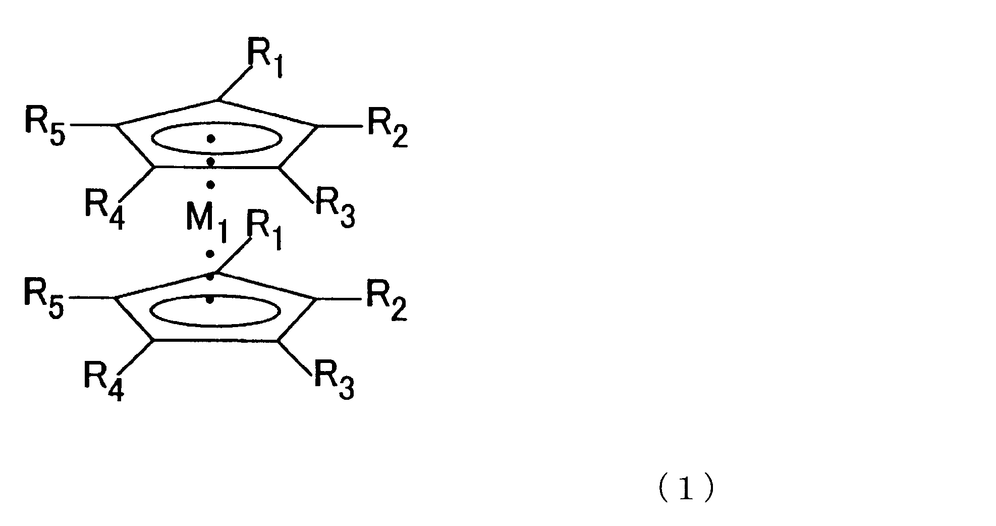
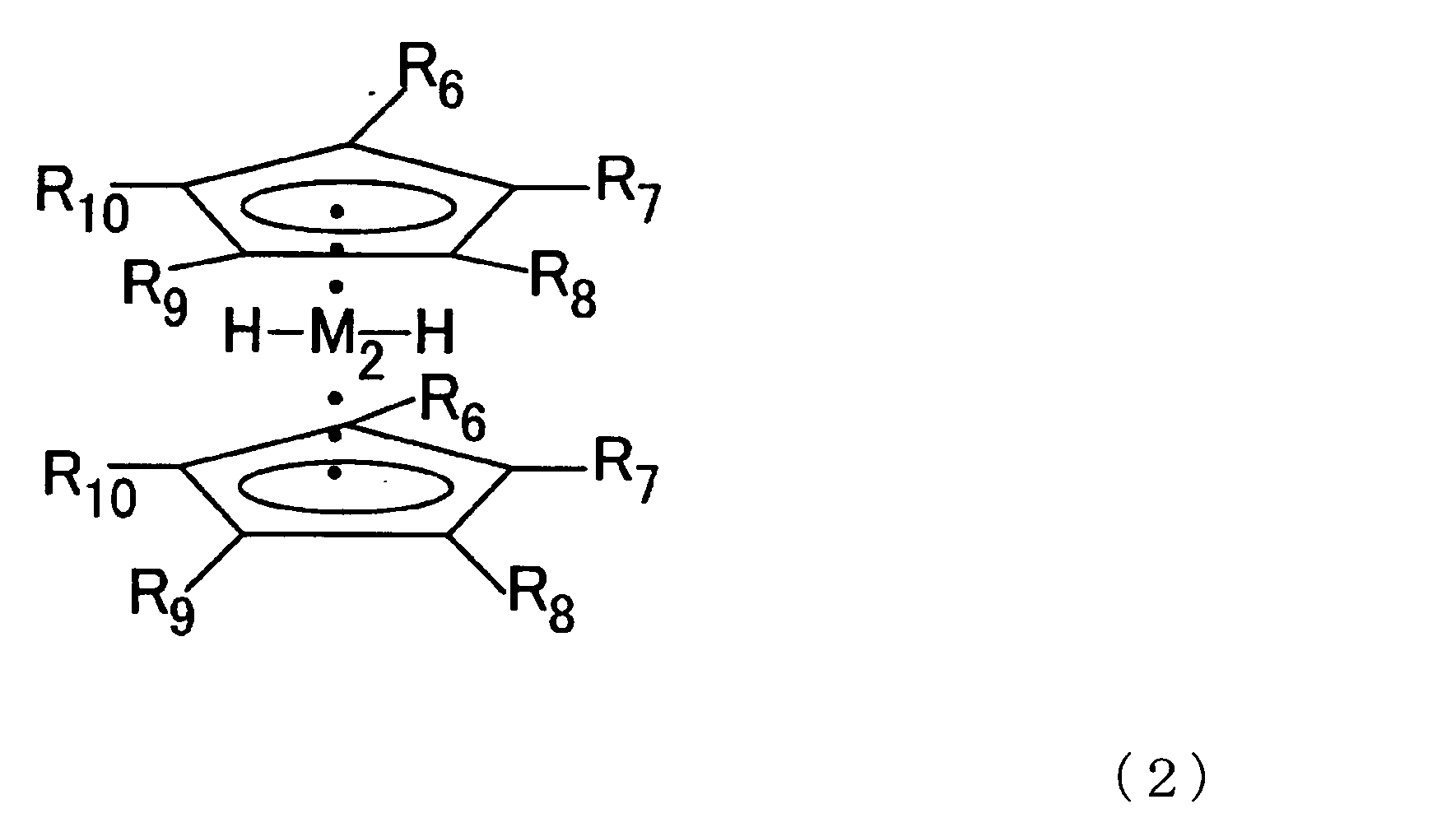
(4)また、上記(1)と(2)の製膜方法は、前記有機金属化合物原料が、下記化学式(2)で示される有機金属化合物を含むことが好ましい。ただし、化学式(2)において、M2はタングステン、モリブデンまたはチタンであり、R6~R10は水素またはnが1以上のCnH2n+1で表される炭化水素である。
(5)また、上記(1)と(2)の製膜方法は、前記有機金属化合物原料が、下記化学式(3)で示される有機金属化合物を含むことが好ましい。ただし、化学式(3)において、M3は白金、ニオブ、ジルコニウムまたはチタンであり、R11~R15は水素またはnが1以上のCnH2n+1で表される炭化水素であり、R16~R18はnが1以上のCnH2n+1で表される炭化水素である。
(6)また、上記(1)から(5)の製膜方法は、前記反応性ガスが、アンモニア、ジメチルヒドラジン、メチルアミン、ジメチルアミン、シラン、ジシランおよび水素のうち、少なくとも1つ以上を含むことが好ましい。
(7)また、上記(1)から(6)の製膜方法は、前記金属触媒体が、タングステン、白金、ロジウムおよびルテニウムのうち、少なくとも1つ以上を含むことが好ましい。
(8)また、上記(1)から(7)の製膜方法は、前記反応性ガス搬送工程の間のみ、前記金属触媒体を通電によって加熱することが好ましい。
(9)また、上記(1)から(8)の製膜方法は、前記原料搬送工程と前記反応性ガス搬送工程を交互に繰り返すとともに、それぞれの工程の間において真空チャンバー内の残留ガスを除去するパージ工程を有することが好ましい。
(10)また、上記(1)から(9)の製膜方法は、前記反応性ガス搬送工程において、真空チャンバー内の圧力を1.33×10²Pa以下にすることが好ましい。
(11)また、上記(1)から(10)の製膜方法は、前記原料搬送工程において、前記有機金属化合物原料を2種類以上用い、同時または順次に製膜対象物上に搬送することが好ましい。
(12)本発明の第2の態様は、上記(1)から(11)のいずれかに記載の金属薄膜の製膜方法によって製膜したことを特徴とする金属薄膜である。
(13)また、本発明の第3の態様は、製膜対象物を内部に載置自在な真空チャンバーと、該真空チャンバー内に載置された製膜対象物上に、有機金属化合物原料を搬送可能な原料搬送手段と、前記真空チャンバー内に載置された製膜対象物上に、加熱された金属触媒体と接触した後の反応性ガスを搬送可能な反応性ガス搬送手段と、を有することを特徴とする金属薄膜の製膜装置である。
なお化学式(1)から(3)で示される有機金属化合物中にCnH2n+1で表される炭化水素が含まれる時、nは任意で選択できる整数であり、1~15であることが好ましく、1~10であることがより好ましく、1~5が更に好ましく、1~3が特に好ましい。CnH2n+1の具体例としては、メチル、エチル及びブチルなどが挙げられる。R1~R5は互いに同じであっても異なっていても良い。R6~R10は互いに同じであっても異なっていても良い。R11~R18は互いに同じであっても異なっていても良い。例えば、有機金属化合物に含まれるRが全て水素でも良いし、全てのRや、1~8個や2~4個のRが、任意で選ばれる炭化水素であっても良い。
なお化学式(1)から(3)で示される有機金属化合物中にCnH2n+1で表される炭化水素が含まれる時、nは任意で選択できる整数であり、1~15であることが好ましく、1~10であることがより好ましく、1~5が更に好ましく、1~3が特に好ましい。CnH2n+1の具体例としては、メチル、エチル及びブチルなどが挙げられる。R1~R5は互いに同じであっても異なっていても良い。R6~R10は互いに同じであっても異なっていても良い。R11~R18は互いに同じであっても異なっていても良い。例えば、有機金属化合物に含まれるRが全て水素でも良いし、全てのRや、1~8個や2~4個のRが、任意で選ばれる炭化水素であっても良い。
本発明によれば、低不純物で、段差被覆性がよく、高真空を使わずに金属薄膜を製膜することができる。
以下、本発明を適用した一実施形態である金属薄膜の製膜装置および金属薄膜の製膜方法について、図面を参照して説明する。本発明の好ましい例が具体的に説明されるが、本発明はこれらの例のみに限定されることは無い。本発明の趣旨を逸脱しない範囲で、構成の付加、省略、置換、その他の変更が可能である。
<金属薄膜の製膜装置>
まず、本実施形態の金属薄膜の製膜装置について説明する。
本実施形態の金属薄膜の製膜装置は、HWALD法による金属薄膜の製膜が可能な装置である。
まず、本実施形態の金属薄膜の製膜装置について説明する。
本実施形態の金属薄膜の製膜装置は、HWALD法による金属薄膜の製膜が可能な装置である。
具体的には、図1に示すように、製膜装置1は、減圧可能な真空チャンバー2と、有機金属化合物原料を搬送可能な原料搬送手段3と、反応性ガスを搬送可能な反応性ガス搬送手段4と、を有している。
真空チャンバー2内には、載置台5が設けられており、この載置台5には基板6(製膜対象物)が自在に載置できるように構成されている。載置台5の内部にはヒーター(図示略)が設けられており、基板6を加熱できるように構成されている。なお製膜対象物の組成や形状やサイズは、特に問題のない限り、任意で選択して良い。
また、真空チャンバー2には、排気管(図示略)および開閉弁(図示略)を介して排気ポンプ7が接続されており、これにより排気可能なように構成されている。なお、真空チャンバー2内には、圧力計(図示略)が設けられており、これにより圧力が測定できるようになっている。
また、真空チャンバー2には、排気管(図示略)および開閉弁(図示略)を介して排気ポンプ7が接続されており、これにより排気可能なように構成されている。なお、真空チャンバー2内には、圧力計(図示略)が設けられており、これにより圧力が測定できるようになっている。
また、真空チャンバー2内には、後述する反応性ガスが接触する金属触媒体8が設けられている。金属触媒体8としては、HWCVD法等に用いられる周知なものを用いてよい。単一元素からなる金属でもよく、あるいは、各種の合金でもよい。特に、実質的にタングステン、白金、ロジウムまたはルテニウムからなることが好ましい。これらの金属からなる金属触媒体8を用いることで、製膜温度を低温にすることができることから、副反応の進行や基板中での物質拡散を抑制するとともに、段差被覆性を向上させることができる。本発明では製膜温度は必要に応じて選択できるが、一例を挙げれば、例えば100~650℃の範囲が挙げられる。また好ましい一例として100~400℃の範囲内であってよく、より好ましくは250~350℃の範囲内である。
また、金属触媒体8は、電源9と接続されており、通電によって加熱されるように構成されている。この通電によって加熱された金属色媒体8と接触することで、反応性ガスは活性種へと活性化される。
なお、金属触媒体8は、真空チャンバー2内に配置してもよいし、真空チャンバー2とはシャッター(図示略)によって仕切られた別の上流側のチャンバー(図示略)内に設置してもよい。
なお、金属触媒体8は、真空チャンバー2内に配置してもよいし、真空チャンバー2とはシャッター(図示略)によって仕切られた別の上流側のチャンバー(図示略)内に設置してもよい。
また、真空チャンバー2には、ガス噴出部10が設けられており、このガス噴出部10に、原料搬送手段3と反応性ガス搬送手段4が接続されている。
原料搬送手段3は、原料供給源11と、原料供給源11に接続された配管12と、配管12に取り付けられたバルブ13とから概略構成されており、配管12はガス噴出部10に接続されている。また、配管12は、バルブ13よりも上流側(原料供給源11側)において分岐しており、分岐した配管14は、バルブ15を介して配管16と接続されている。
原料搬送手段3は、原料供給源11と、原料供給源11に接続された配管12と、配管12に取り付けられたバルブ13とから概略構成されており、配管12はガス噴出部10に接続されている。また、配管12は、バルブ13よりも上流側(原料供給源11側)において分岐しており、分岐した配管14は、バルブ15を介して配管16と接続されている。
原料供給源11は、有機金属化合物原料を供給可能であれば、どのような構成でもよい。本実施形態では有機金属化合物が貯蔵されている原料貯液槽17と、原料貯液槽17の液相部分に接続された配管18と、原料貯液槽17の気相部分に接続された配管12から構成されている。この場合、配管18にヘリウムなどの不活性ガスを原料貯液槽17に導入すると、有機金属化合物原料を同伴して配管12から導出することができる。
なお、本実施形態では、有機金属化合物原料として常温で液体状のものを用いることを想定し、バブリングによる気化が可能な構成を採用した。しかしながら、必ずしもこのような構成である必要はない。例えば、有機金属化合物原料として常温で気体状のものを原料として用いてもよく、また液体状のものを用いた場合も気化器による気化や加熱による気化によってガス化してもよい。
以上のように構成された原料搬送手段3によって、原料貯液槽17の気相部分から取り出されたガス化した有機金属化合物原料は、ガス噴出部10を介して真空チャンバー2内に導入されて、基板6上に搬送される。
反応性ガス搬送手段4は、反応性ガス供給源21と、この反応性ガス供給源21と接続された配管22と、配管22に取り付けられたバルブ23とから概略構成されており、配管22はガス噴出部10に接続されている。反応性ガス供給源21は、反応性ガスを供給可能であるのならば、どのような構成であっても構わない。
また、配管22は、バルブ23よりも上流側(反応性ガス供給源21側)において分岐しており、分岐した配管24は、バルブ25を介して配管16と接続されている。
また、配管22は、バルブ23よりも上流側(反応性ガス供給源21側)において分岐しており、分岐した配管24は、バルブ25を介して配管16と接続されている。
このように構成された反応性ガス搬送手段4によって、反応性ガス供給源21から導出した反応性ガスは、ガス噴出部10を介して真空チャンバー2内に導入し、金属触媒体8と接触した上で、基板6上に搬送される。
<金属薄膜の製膜方法>
次に、上記した製膜装置1を用いた金属薄膜の製膜方法について説明する。
本実施形態の金属薄膜の製膜方法は、原料搬送工程と、反応性ガス搬送工程とを有しており、まずこれらについて説明する。
次に、上記した製膜装置1を用いた金属薄膜の製膜方法について説明する。
本実施形態の金属薄膜の製膜方法は、原料搬送工程と、反応性ガス搬送工程とを有しており、まずこれらについて説明する。
まず原料搬送工程について説明する。
原料搬送工程は、具体的には有機金属化合物原料を真空チャンバー2内に載置された基板6上に搬送する工程である。基板は問題のない限り任意で選択してよい。
有機金属化合物原料としては、種々のものを用いることが可能である。しかしながら、炭素原子、窒素原子、水素原子、ケイ素原子、リン原子、ホウ素原子および金属原子からなる群から選択される1または2以上の原子のみからなることが好ましい。上記金属原子は必要に応じて選択できるが、例えばコバルト、マンガン、ニッケル、ルテニウム、タングステン、モリブデン、白金、チタン等の原子が挙げられる。このような材料を選択することで、製膜された金属薄膜にハロゲンや酸素が含まれるのを防止することができ、膜質の低下を防止することができる。
原料搬送工程は、具体的には有機金属化合物原料を真空チャンバー2内に載置された基板6上に搬送する工程である。基板は問題のない限り任意で選択してよい。
有機金属化合物原料としては、種々のものを用いることが可能である。しかしながら、炭素原子、窒素原子、水素原子、ケイ素原子、リン原子、ホウ素原子および金属原子からなる群から選択される1または2以上の原子のみからなることが好ましい。上記金属原子は必要に応じて選択できるが、例えばコバルト、マンガン、ニッケル、ルテニウム、タングステン、モリブデン、白金、チタン等の原子が挙げられる。このような材料を選択することで、製膜された金属薄膜にハロゲンや酸素が含まれるのを防止することができ、膜質の低下を防止することができる。
更に、有機金属化合物原料は、上記化学式(1)で示される有機金属化合物、または上記化学式(2)で示される有機金属化合物、または上記化学式(3)で示される有機金属化合物を含むことがより好ましい。有機金属化合物原料はこれらの有機金属化合物を0~100重量%含むことが好ましく、50~100重量%含むことがより好ましく、75~100重量%含むことが更に好ましく、90~100重量%含むことが特に好ましい。有機金属化合物原料は、これらの有機金属化合物(1)~(3)のいずれかの化合物のみからなってもよい。ただし、化学式(1)において、M1はコバルト、ニッケル、鉄、マンガン、ルテニウムおよびクロムのいずれかであり、R1~R5は水素またはnが1以上のCnH2n+1で表される炭化水素である。また、化学式(2)において、M2はタングステン、モリブデンまたはチタンであり、R6~R10は水素またはnが1以上のCnH2n+1で表される炭化水素である。また、化学式(3)において、M3は白金、ニオブ、ジルコニウムまたはチタンであり、R11~R15は水素またはnが1以上のCnH2n+1で表される炭化水素であり、R16~R18はnが1以上のCnH2n+1で表される炭化水素である。
なお、化学式(1)または化学式(2)で示される有機金属原料は、ビスシクロペンタジエニル化合物(通称:メタロセン)であり、様々な金属で合成が報告されている。
このような材料を選択することで、より不純物の少ない金属薄膜を製膜することができる。加えて、メタロセンを用いた場合は、HWALD法を採用することで減圧下でも製膜することが可能であるため、段差被覆性の良い金属薄膜を得ることができる。
このような材料を選択することで、より不純物の少ない金属薄膜を製膜することができる。加えて、メタロセンを用いた場合は、HWALD法を採用することで減圧下でも製膜することが可能であるため、段差被覆性の良い金属薄膜を得ることができる。
また、有機金属化合物原料は、常温で気体状であればそのまま用いることができ、液体状のものであれば、ヘリウムなどの不活性ガスを用いたバブリングによる気化、気化器による気化、または加熱による気化によってガス化して用いればよい。また、ヘリウムなどをキャリアガスとして、有機金属化合物原料と併せて用いてもよい。
例えば、常温で液体状の有機金属化合物材料を、バブリングによって気化して用いる場合は、図1に示すように、配管18を介して有機金属化合物材料が貯蔵されている原料貯液槽17の液相部分に不活性ガスを導入する。その上で、原料貯液槽17の気相部分からガス化した有機金属化合物材料を、配管12を介して抜き出せばよい。
気化した有機金属化合物材料は、配管12を介してガス噴出部10に導入され、その後真空チャンバー2内に導入される。この際、バルブ15は閉じており、バルブ13は開いた状態となっている。
そして、真空チャンバー2内に導入された有機金属化合物材料は、基板6に搬送される。
以上のようにして、有機金属化合物原料は、真空チャンバー2内に載置された基板6上に搬送される。
そして、真空チャンバー2内に導入された有機金属化合物材料は、基板6に搬送される。
以上のようにして、有機金属化合物原料は、真空チャンバー2内に載置された基板6上に搬送される。
なお、原料搬送工程においては、真空チャンバー2内に配置された金属触媒体8には、通電することなく、加熱していない状態で保つことが好ましい。これにより、基板表面の温度上昇を抑制するほか、金属触媒体の劣化を防止する、及び、消費電力を低減できるという効果が得られる。
また、有機金属化合物原料は、1種類である必要はなく、2種類以上であっても構わない。2種類以上用いる場合は、同時または順次に基板6上に搬送すればよい。
次に、反応性ガス搬送工程を説明する。
反応性ガス搬送工程は、具体的には反応性ガスを、加熱された金属触媒体8に接触させた後に、真空チャンバー2内に載置された基板6上に搬送する工程である。
反応性ガスとしては、種々のものを用いることができるが、炭素原子、窒素原子、水素原子、ケイ素原子、リン原子、ホウ素原子および金属原子から選択される1または2以上の原子のみからなることが好ましい。上記金属原子は必要に応じて選択できるが、例えばコバルト、マンガン、ルテニウム、タングステン、モリブデン、白金、チタン、アルミニウム、ガリウム、スズ等の原子が挙げられる。このような材料を選択することで、製膜された金属薄膜にハロゲンや酸素が含まれるのを防止することができ、膜質の低下を防止することができる。
反応性ガス搬送工程は、具体的には反応性ガスを、加熱された金属触媒体8に接触させた後に、真空チャンバー2内に載置された基板6上に搬送する工程である。
反応性ガスとしては、種々のものを用いることができるが、炭素原子、窒素原子、水素原子、ケイ素原子、リン原子、ホウ素原子および金属原子から選択される1または2以上の原子のみからなることが好ましい。上記金属原子は必要に応じて選択できるが、例えばコバルト、マンガン、ルテニウム、タングステン、モリブデン、白金、チタン、アルミニウム、ガリウム、スズ等の原子が挙げられる。このような材料を選択することで、製膜された金属薄膜にハロゲンや酸素が含まれるのを防止することができ、膜質の低下を防止することができる。
更に、反応性ガスは、アンモニア、ジメチルヒドラジン、メチルアミン、ジメチルアミン、シラン、ジシランおよび水素のうち、少なくとも1つ以上を含むことがより好ましい。これらのうち、いずれか一種のみからなるガスであっても良い。このような材料を選択することで、より低不純物で、段差被覆性の良い金属薄膜を製膜することができる。
特に、有機金属化合物材料としてメタロセンを採用した場合は、反応性ガスは窒素原子を含有するガスであることが好ましい。
メタロセンに含有される金属原子にHやNH2が結合していない場合は、金属原子を解離させるために多くのエネルギーが必要となる。これに対し、金属原子にHが結合している場合、金属原子を解離するためにはそれ程のエネルギーは必要とせず、特に、金属原子がNH2と結合している場合、金属原子を解離させるために必要とするエネルギーは小さくて済む。段差被覆性の良好な薄膜を製膜するために1Paから133Pa程度の減圧条件下で製膜する場合や400℃以下の温度条件で製膜する必要のある場合、反応性ガスは窒素原子を含有するものが好ましい。
メタロセンに含有される金属原子にHやNH2が結合していない場合は、金属原子を解離させるために多くのエネルギーが必要となる。これに対し、金属原子にHが結合している場合、金属原子を解離するためにはそれ程のエネルギーは必要とせず、特に、金属原子がNH2と結合している場合、金属原子を解離させるために必要とするエネルギーは小さくて済む。段差被覆性の良好な薄膜を製膜するために1Paから133Pa程度の減圧条件下で製膜する場合や400℃以下の温度条件で製膜する必要のある場合、反応性ガスは窒素原子を含有するものが好ましい。
例えば、コバルトセン(上記化学式(1)のM1がコバルトのもの)の場合、図2Aに示すように、コバルトにHやNH2が結合していない場合、コバルトセンからシクロペンタジエンを離脱させるのには50.5kcal/mol必要である。これに対し、図2Bに示すように、コバルトにHが結合している場合、コバルトセンからシクロペンタジエンを離脱させるのには29.1kcal/molのみしか必要とせず、図2Cに示すように、コバルトにNH2が結合している場合は、15.2kcal/mol程度しか必要とされない。
なお、反応性ガスは、他の不活性ガスを用いて希釈させることもできる。
なお、反応性ガスは、他の不活性ガスを用いて希釈させることもできる。
反応性ガス供給源21から供給される反応性ガスは、配管22を介してガス噴出部10に導入され、その後真空チャンバー2内に導入される。この際、バルブ25は閉じており、バルブ23は開いた状態となっている。また、反応性ガスを真空チャンバー2内に導入する際は、ガス噴出部10に設けられたシャワーヘッド26を介して導入してもよい。
そして、真空チャンバー2内に導入された反応性ガスは、通電等によって加熱された金属触媒体8と接触した後に、基板6上に搬送される。
この加熱された金属触媒体8と接触することによって、反応性ガスが、NXnラジカル、SiXnラジカル、BXnラジカル(Xは水素または炭化水素、nは1から3の整数)およびHラジカルのうち少なくとも1つの活性種に活性化されることが好ましい。
以上のようにして、反応性ガスは、加熱された金属触媒体8に接触させた後に、真空チャンバー2内に載置された基板6上に搬送される。
この加熱された金属触媒体8と接触することによって、反応性ガスが、NXnラジカル、SiXnラジカル、BXnラジカル(Xは水素または炭化水素、nは1から3の整数)およびHラジカルのうち少なくとも1つの活性種に活性化されることが好ましい。
以上のようにして、反応性ガスは、加熱された金属触媒体8に接触させた後に、真空チャンバー2内に載置された基板6上に搬送される。
次に、原料搬送工程と、反応性ガス搬送工程の関係について説明する。
本実施形態の金属薄膜の製膜方法は、基本的にはHWALD法による製膜方法である。ただし反応性ガスを加熱された金属触媒体に接触させる点で従来の方法と異なる。
したがって、具体的には、基板6上に有機金属化合物原料を搬送し、基板6上に有機金属化合物原料を飽和吸着させた状態で、有機金属化合物原料の供給を止め、その後基板6上に反応性ガスを供給することで、有機金属化合物原料を基板6上に製膜する。この工程を1サイクルとして、基板6上に所望の膜厚の金属薄膜が製膜されるまで、当該サイクルを複数回行う。サイクルの数は任意に選択してよいが、例えば50~1000回、より好ましくは70~700回、更に好ましくは80~500回、特に好ましくは100~400回等が例として挙げられる。反応性ガスや有機金属化合物原料の流量や供給時間などは必要に応じて選択してよい。
本実施形態の金属薄膜の製膜方法は、基本的にはHWALD法による製膜方法である。ただし反応性ガスを加熱された金属触媒体に接触させる点で従来の方法と異なる。
したがって、具体的には、基板6上に有機金属化合物原料を搬送し、基板6上に有機金属化合物原料を飽和吸着させた状態で、有機金属化合物原料の供給を止め、その後基板6上に反応性ガスを供給することで、有機金属化合物原料を基板6上に製膜する。この工程を1サイクルとして、基板6上に所望の膜厚の金属薄膜が製膜されるまで、当該サイクルを複数回行う。サイクルの数は任意に選択してよいが、例えば50~1000回、より好ましくは70~700回、更に好ましくは80~500回、特に好ましくは100~400回等が例として挙げられる。反応性ガスや有機金属化合物原料の流量や供給時間などは必要に応じて選択してよい。
この際、有機金属化合物原料を搬送しただけでは、基板6上に金属薄膜は製膜されず、反応性ガスを搬送して初めて製膜される。そして、基板6上に飽和吸着している有機金属化合物原料のみが製膜されるので、1原子ないし数原子単位で薄膜を製膜することになる。
したがって、所望の膜厚とするためには、原料搬送工程と反応性ガス搬送工程を、それぞれ交互に繰り返すこととなる。その際それぞれの工程の間において、真空チャンバー2内の残留ガスを除去するパージ工程を有することが好ましい。
このようなパージ工程を有することで、より精度よく金属薄膜を製膜することができる。
このようなパージ工程を有することで、より精度よく金属薄膜を製膜することができる。
原料搬送工程と反応性ガス搬送工程の切替は、バルブ13、23の開閉で制御すればよい。また、原料搬送工程中は、バルブ23を閉じバルブ25を開くことで、反応性ガス供給源21から導出する反応性ガスを配管24,16を介して系外に排出するようにしてもよい。また、逆に、反応性ガス搬送工程中は、バルブ13を閉じバルブ15を開くことで、有機金属化合物原料を配管14,16を介して系外に排出すれようにしてもよい。
以上のようにして、原料搬送工程と反応性ガス搬送工程を交互に行うことで、基板6上に金属薄膜が製膜される。
以上のようにして、原料搬送工程と反応性ガス搬送工程を交互に行うことで、基板6上に金属薄膜が製膜される。
なお、真空チャンバー2内の圧力を、反応性ガス搬送工程において、1.33×10²Pa(=1Torr)以下にすることが好ましい。反応性ガス搬送工程における真空チャンバー2内の圧力の下限は任意で選択されるが、0.013Pa以上であることが好ましい。また真空チャンバー2内の圧力を、製膜プロセスの全工程において、1.33×10²Pa(=1Torr)以下にすることがより好ましく、製膜プロセスの全工程において6.65×10Pa(=0.5Torr)以下にすることが更に好ましい。製膜プロセスの全工程における真空チャンバー2内の圧力の下限は任意で選択されるが、0.013Pa以上であることが好ましい。
このような減圧下で製膜することによって、製膜された金属薄膜の段差被覆性がよりよくなる。
このような減圧下で製膜することによって、製膜された金属薄膜の段差被覆性がよりよくなる。
本実施形態の金属薄膜の製膜方法は、原料搬送工程と反応性ガス搬送工程を有するので、低不純物で、段差被覆性がよい金属薄膜を製膜することができる。
また、製膜プロセスにおいて、高真空が要求されないので、製造装置が高額にならない。加えて、原料搬送工程と反応性ガス搬送工程を交互に行うので、金属触媒体上で金属薄膜が堆積するのを防止することができる。
また、製膜プロセスにおいて、高真空が要求されないので、製造装置が高額にならない。加えて、原料搬送工程と反応性ガス搬送工程を交互に行うので、金属触媒体上で金属薄膜が堆積するのを防止することができる。
また、有機金属化合物原料または/および反応性ガスが、炭素原子、窒素原子、水素原子、ケイ素原子、リン原子、ホウ素原子および金属原子からなる群から選択される1または2以上の原子のみからなるので、製膜された金属薄膜にハロゲンや酸素が混入するのを防止することができ、良好な膜質の金属薄膜を製膜することができる。
以上、本発明を実施形態に基づき説明したが、本発明は、上記実施形態に限定されるものではなく、その要旨を逸脱しない範囲で種々変更可能であることは言うまでもない。
以下、本発明を実施例および比較例により、更に詳細に説明する。ただし、本発明は以下の実施例等によって何ら限定されるものではない。
(実施例1)
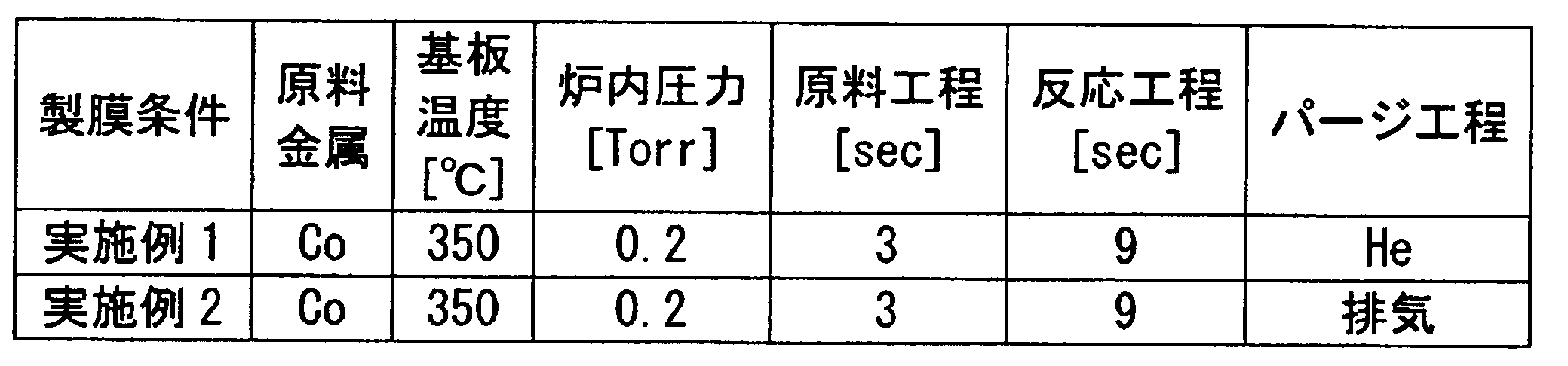
実施例1では、図1に示した金属薄膜の製膜装置を用いた。なお真空チャンバーの容量は0.02m3であり、基板はサイズが直径2インチのシリコンウェハを用いた。表1に示すように、基板を350℃に保ち、自動圧力制御器(APC)を用いて真空チャンバー内の圧力を2.66×10Pa(=0.2Torr)に保った。また、有機金属化合物原料としてビスシクロペンタジエニルコバルト(コバルトセン)を、反応性ガスとしてアンモニアを、金属触媒体としてタングステンワイヤーを用いた。
実施例1では、図1に示した金属薄膜の製膜装置を用いた。なお真空チャンバーの容量は0.02m3であり、基板はサイズが直径2インチのシリコンウェハを用いた。表1に示すように、基板を350℃に保ち、自動圧力制御器(APC)を用いて真空チャンバー内の圧力を2.66×10Pa(=0.2Torr)に保った。また、有機金属化合物原料としてビスシクロペンタジエニルコバルト(コバルトセン)を、反応性ガスとしてアンモニアを、金属触媒体としてタングステンワイヤーを用いた。
製膜方法としては、まずコバルトセンの入った原料ボトルを50℃に加熱し、流量30sccmのヘリウムによって、原料蒸気を同伴させて真空チャンバー内に3秒間供給する。次いで、流量30sccmのヘリウムによるパージを2秒行う。
その後、流量30sccmのアンモニアを真空チャンバー内に9秒間供給する。その間タングステンワイヤーに3Aの電流を通電させて赤熱するまで加熱する。
そして、流量30sccmのヘリウムによるパージを2秒行う。
以上の工程を1サイクルとして、図3に示すように、原料供給、パージ、アンモニアの供給と通電、パージを、400回繰り返した。
その後、流量30sccmのアンモニアを真空チャンバー内に9秒間供給する。その間タングステンワイヤーに3Aの電流を通電させて赤熱するまで加熱する。
そして、流量30sccmのヘリウムによるパージを2秒行う。
以上の工程を1サイクルとして、図3に示すように、原料供給、パージ、アンモニアの供給と通電、パージを、400回繰り返した。
その結果、実施例1では、表2に示すように、製膜速度は、0.04nm/サイクルであり、得られた膜の抵抗率は20μΩcmであった。また、製膜後、X線光電子分光法(XPS)によって得られた金属薄膜の組成を調べたところ、膜中の炭素、酸素、窒素はともに検出下限である1%以下であった。
(実施例2)
実施例2では、パージ工程においてヘリウムを流通させるのではなく、真空引きとし、表1に示すように、その他の条件は実施例1と同様の条件で金属薄膜を製膜した。
実施例2では、表2に示すように、製膜速度は、0.05nm/サイクルであり、抵抗率は20μΩcmであった。また、製膜後、X線光電子分光法(XPS)によって得られた金属薄膜の組成を調べたところ、炭素、酸素、窒素ともに検出下限である1%以下であった。
実施例2では、パージ工程においてヘリウムを流通させるのではなく、真空引きとし、表1に示すように、その他の条件は実施例1と同様の条件で金属薄膜を製膜した。
実施例2では、表2に示すように、製膜速度は、0.05nm/サイクルであり、抵抗率は20μΩcmであった。また、製膜後、X線光電子分光法(XPS)によって得られた金属薄膜の組成を調べたところ、炭素、酸素、窒素ともに検出下限である1%以下であった。

(実施例3~5)
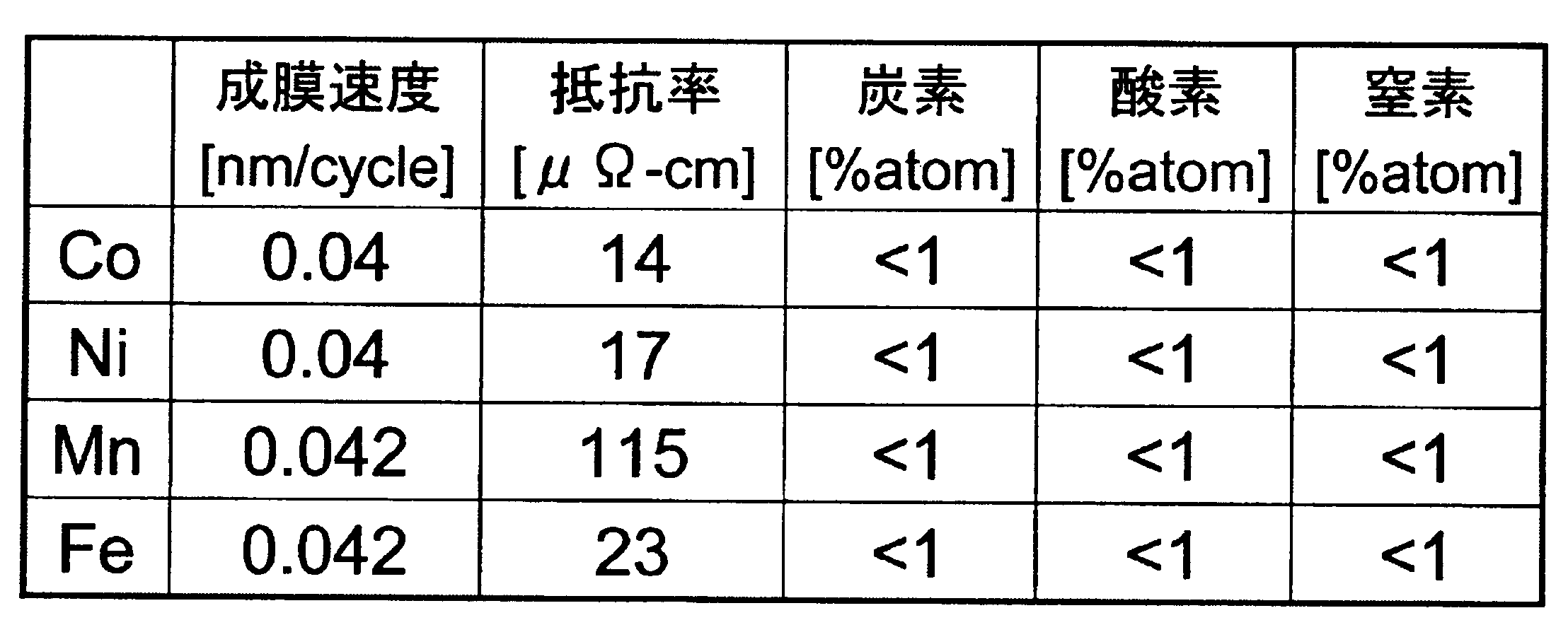
実施例3~5では、有機金属化合物原料として、コバルトセンの代わりに、それぞれニッケロセン、マンガノセン、又はフェロセンを用い、その他の条件は実施例1と同様の条件とした場合の製膜速度および金属薄膜の組成について、シミュレーションを行った。結果を表3に示す。表3では、上の行から順に、実施例1(Co)、実施例2(Ni)、実施例3(Mn)、及び実施例4(Fe)の結果が示される。
実施例3~5では、有機金属化合物原料として、コバルトセンの代わりに、それぞれニッケロセン、マンガノセン、又はフェロセンを用い、その他の条件は実施例1と同様の条件とした場合の製膜速度および金属薄膜の組成について、シミュレーションを行った。結果を表3に示す。表3では、上の行から順に、実施例1(Co)、実施例2(Ni)、実施例3(Mn)、及び実施例4(Fe)の結果が示される。
(実施例6)
実施例6では、2つの原料ボトル等を備える以外は実施例1と同様な製膜装置を用い、基板を350℃に保ち、自動圧力制御器(APC)を用いて真空チャンバー内の圧力を2.66×10Pa(=0.2Torr)に保った。
有機金属化合物原料としては、ビスシクロペンタジエニルコバルト(コバルトセン)とビスシクロペンタジエニルタングステンステンジハイドライドの2種類を用い、反応性ガスとしてアンモニアを、金属触媒体としてタングステンワイヤーを用いた。
実施例6では、2つの原料ボトル等を備える以外は実施例1と同様な製膜装置を用い、基板を350℃に保ち、自動圧力制御器(APC)を用いて真空チャンバー内の圧力を2.66×10Pa(=0.2Torr)に保った。
有機金属化合物原料としては、ビスシクロペンタジエニルコバルト(コバルトセン)とビスシクロペンタジエニルタングステンステンジハイドライドの2種類を用い、反応性ガスとしてアンモニアを、金属触媒体としてタングステンワイヤーを用いた。
製膜方法としては、2種類の有機金属化合物原料を同時に供給する方法を採用した。具体的には、まずコバルトセンの入った原料ボトルを50℃に加熱するとともに、ビスシクロペンタジエニルタングステンステンジハイドライドの入った原料ボトルを100℃に加熱した。その後、それぞれのボトルに対して流量30sccmのヘリウムを通気することで原料蒸気を同伴させ、コバルトセンおよびビスシクロペンタジエニルタングステンステンジハイドライドを同時に真空チャンバー内に3秒間供給する。次いで、流量30sccmのヘリウムによるパージを2秒行う。
その後、流量30sccmのアンモニアを真空チャンバー内に9秒間供給する。その間タングステンワイヤーに3Aの電流を通電させて赤熱するまで加熱する。
そして、流量30sccmのヘリウムによるパージを2秒行う。
以上の工程を1サイクルとして、図3に示すように、原料供給、パージ、アンモニアの供給と通電、パージを400回繰り返した。
そして、流量30sccmのヘリウムによるパージを2秒行う。
以上の工程を1サイクルとして、図3に示すように、原料供給、パージ、アンモニアの供給と通電、パージを400回繰り返した。
その結果、実施例6では、製膜速度は、0.04nm/サイクルであり、抵抗率は25μΩcmであった。また、製膜後、X線光電子分光法(XPS)によって得られた金属薄膜の組成を調べたところ、コバルト組成は95%、タングステン組成は5%であり、炭素、酸素、窒素はともに検出下限である1%以下であった。
(実施例7)
実施例7では、2つの原料ボトル等を備える以外は実施例1と同様な製膜装置を用い、基板を350℃に保ち、自動圧力制御器(APC)を用いて真空チャンバー内の圧力を2.66×10Pa(=0.2Torr)に保った。
有機金属化合物原料としては、ビスシクロペンタジエニルコバルト(コバルトセン)とビスシクロペンタジエニルタングステンステンジハイドライドの2種類を用い、反応性ガスとしてアンモニアを、金属触媒体としてタングステンワイヤーを用いた。
実施例7では、2つの原料ボトル等を備える以外は実施例1と同様な製膜装置を用い、基板を350℃に保ち、自動圧力制御器(APC)を用いて真空チャンバー内の圧力を2.66×10Pa(=0.2Torr)に保った。
有機金属化合物原料としては、ビスシクロペンタジエニルコバルト(コバルトセン)とビスシクロペンタジエニルタングステンステンジハイドライドの2種類を用い、反応性ガスとしてアンモニアを、金属触媒体としてタングステンワイヤーを用いた。
製膜する際は、2種類の有機金属化合物原料を順次に供給する方法を採用した。具体的には、まずコバルトセンの入った原料ボトルを50℃に加熱するとともに、ビスシクロペンタジエニルタングステンステンジハイドライドの入った原料ボトルを100℃に加熱した。その後、それぞれのボトルに対して流量30sccmのヘリウムを通気することで原料蒸気を同伴させて、基板上に順次搬送させた。
具体的には、まずコバルトセンを真空チャンバー内に3秒間供給する。次いで、流量30sccmのヘリウムによるパージを2秒行う。その後、流量30sccmのアンモニアを真空チャンバー内に9秒間供給する。その間タングステンワイヤーに3Aの電流を通電させて赤熱するまで加熱する。そして、流量30sccmのヘリウムによるパージを2秒行う。
その後、ビスシクロペンタジエニルタングステンステンジハイドライドを真空チャンバー内に3秒間供給する。次いで、流量30sccmのヘリウムによるパージを2秒行う。その後、流量30sccmのアンモニアを真空チャンバー内に9秒間供給する。その間タングステンワイヤーに3Aの電流を通電させて赤熱するまで加熱する。そして、流量30sccmのヘリウムによるパージを2秒行う。
以上の工程を1サイクルとして、図4に示すように、コバルトセンの供給、パージ、アンモニアの供給と通電、パージ、ビスシクロペンタジエニルタングステンステンジハイドライドの供給、パージ、アンモニアの供給と通電、パージを200回繰り返した。
その結果、実施例7では、製膜速度は、0.04nm/サイクルであり、抵抗率は25μΩcmであった。また、製膜後、X線光電子分光法(XPS)によって得られた金属薄膜の組成を調べたところ、コバルト組成は90%、タングステン組成は10%、炭素、酸素、窒素ともに検出下限である1%以下であった。
(比較例1)
比較例1では、熱CVD法による実験を行った。
なお熱CVD法に用いた装置は、実施例1に用いた装置と同じものであるが、タングステンフィラメントを取り外しているという違いがある装置である。具体的には、表4に示す条件のように、基板を400℃に保ち、自動圧力制御器(APC)を用いて真空チャンバー内の圧力を3.99×10²Pa(=3Torr)に保った。
そして、コバルトセンの入った原料ボトルを50℃に加熱し、流量30sccmのヘリウムによって、原料蒸気を同伴させて真空チャンバー内に供給すると同時に、水素ガスを流量30sccmで真空チャンバー内に供給した。
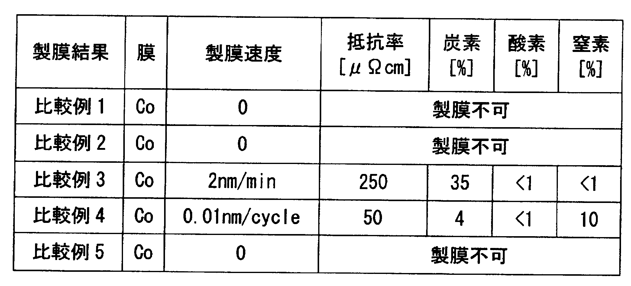
その結果、表5に示すように、60分間供給しても金属薄膜は製膜されなかった。
比較例1では、熱CVD法による実験を行った。
なお熱CVD法に用いた装置は、実施例1に用いた装置と同じものであるが、タングステンフィラメントを取り外しているという違いがある装置である。具体的には、表4に示す条件のように、基板を400℃に保ち、自動圧力制御器(APC)を用いて真空チャンバー内の圧力を3.99×10²Pa(=3Torr)に保った。
そして、コバルトセンの入った原料ボトルを50℃に加熱し、流量30sccmのヘリウムによって、原料蒸気を同伴させて真空チャンバー内に供給すると同時に、水素ガスを流量30sccmで真空チャンバー内に供給した。
その結果、表5に示すように、60分間供給しても金属薄膜は製膜されなかった。
(比較例2)
水素ガスの代わりにアンモニアを用いた他は、表4に示すように、比較例1と同じ条件で、実験を行った。
その結果、表5に示すように、60分間供給しても金属薄膜は製膜されなかった。
水素ガスの代わりにアンモニアを用いた他は、表4に示すように、比較例1と同じ条件で、実験を行った。
その結果、表5に示すように、60分間供給しても金属薄膜は製膜されなかった。
(比較例3)
比較例3では、PECVD法による実験を行った。なおPECVD法に用いた装置は、実施例1で用いた装置と同じものであるが、タングステンフィラメントを取り外していること、基板とシャワーヘッドの間で容量結合プラズマを生成できるよう基板側に電極を取り付けた装置である。具体的には、表4に示すように、基板を300℃に保ち、自動圧力制御器(APC)を用いて真空チャンバー内の圧力を3.99×10²Pa(=3Torr)に保った。
そして、コバルトセンの入った原料ボトルを50℃に加熱し、流量30sccmのヘリウムによって、原料蒸気を同伴させて真空チャンバー内に供給すると同時に、水素ガスを流量30sccmで真空チャンバー内に供給した。
それと同時に、シャワーヘッドおよび基板ステージ(載置台)を電極として150WのRFを印加し、容量結合プラズマを発生させた。
比較例3では、PECVD法による実験を行った。なおPECVD法に用いた装置は、実施例1で用いた装置と同じものであるが、タングステンフィラメントを取り外していること、基板とシャワーヘッドの間で容量結合プラズマを生成できるよう基板側に電極を取り付けた装置である。具体的には、表4に示すように、基板を300℃に保ち、自動圧力制御器(APC)を用いて真空チャンバー内の圧力を3.99×10²Pa(=3Torr)に保った。
そして、コバルトセンの入った原料ボトルを50℃に加熱し、流量30sccmのヘリウムによって、原料蒸気を同伴させて真空チャンバー内に供給すると同時に、水素ガスを流量30sccmで真空チャンバー内に供給した。
それと同時に、シャワーヘッドおよび基板ステージ(載置台)を電極として150WのRFを印加し、容量結合プラズマを発生させた。
その結果、表5に示すように、製膜速度は、2nm/minであり、得られた膜の抵抗率は250μΩcmであった。また、製膜後、X線光電子分光法(XPS)によって得られた金属薄膜の組成を調べたところ、酸素、窒素ともに検出下限である1%以下であったが、炭素は35%含まれていた。
(比較例4)
比較例4では、PEALD法による実験を行った。なおPEALD法に用いた装置は、実施例1に用いた装置と同じものであるが、タングステンフィラメントを取り外していること、アンモニアの導入ポートに10cmのガラス管を設け、そこで誘導結合プラズマを生成できるようにガラス管外側に100回巻きのコイルを設けた装置である。具体的には、表4に示すように、基板を250~350℃に保ち、自動圧力制御器(APC)を用いて真空チャンバー内の圧力を2.66Pa(=0.02Torr)に保った。
そして、コバルトセンの入った原料ボトルを50℃に加熱し、流量30sccmのヘリウムによって、原料蒸気を同伴させて真空チャンバー内に3秒間供給する。次いで、流量30sccmのヘリウムによるパージを2秒行う。
その後、流量30sccmのアンモニアを真空チャンバー内に6秒間供給する。その間アンモニア供給ポートにおいて誘導結合プラズマを発生させた。そして、流量30sccmのヘリウムによるパージを2秒行う。
以上の工程を1サイクルとして、原料供給、パージ、アンモニアの供給とプラズマの発生、パージの組み合わせを、400回繰り返した。
比較例4では、PEALD法による実験を行った。なおPEALD法に用いた装置は、実施例1に用いた装置と同じものであるが、タングステンフィラメントを取り外していること、アンモニアの導入ポートに10cmのガラス管を設け、そこで誘導結合プラズマを生成できるようにガラス管外側に100回巻きのコイルを設けた装置である。具体的には、表4に示すように、基板を250~350℃に保ち、自動圧力制御器(APC)を用いて真空チャンバー内の圧力を2.66Pa(=0.02Torr)に保った。
そして、コバルトセンの入った原料ボトルを50℃に加熱し、流量30sccmのヘリウムによって、原料蒸気を同伴させて真空チャンバー内に3秒間供給する。次いで、流量30sccmのヘリウムによるパージを2秒行う。
その後、流量30sccmのアンモニアを真空チャンバー内に6秒間供給する。その間アンモニア供給ポートにおいて誘導結合プラズマを発生させた。そして、流量30sccmのヘリウムによるパージを2秒行う。
以上の工程を1サイクルとして、原料供給、パージ、アンモニアの供給とプラズマの発生、パージの組み合わせを、400回繰り返した。
その結果、表5に示すように、製膜速度は、0.01nm/サイクルであり、得られた膜の抵抗率は50μΩcmであった。また、製膜後、X線光電子分光法(XPS)によって得られた金属薄膜の組成を調べたところ、酸素は検出下限である1%以下であったが、炭素は4%、窒素は10%含まれていた。
(比較例5)
比較例5では、実施例1と略同様に実験を行ったが、表4に示すように、真空チャンバー内の圧力を2.66×10²Pa(=2Torr)とした。その他の条件は実施例1と同様の条件で金属薄膜を製膜した。
その結果、表5に示すように金属薄膜は製膜されなかった。
比較例5では、実施例1と略同様に実験を行ったが、表4に示すように、真空チャンバー内の圧力を2.66×10²Pa(=2Torr)とした。その他の条件は実施例1と同様の条件で金属薄膜を製膜した。
その結果、表5に示すように金属薄膜は製膜されなかった。

本発明は、金属薄膜を用いた製品を製造する製造業において幅広く利用することができる。低不純物で、段差被覆性がよく、高真空を使わない金属薄膜の製膜方法を提供できる。
1 製膜装置
2 真空チャンバー
3 原料搬送手段
4 反応性ガス搬送手段
5 載置台
6 基板
7 排気ポンプ
8 金属触媒体
9 電源
10 ガス噴出部
11 原料供給源
12,14,16,18,22,24 配管
13,15,23,25 バルブ
17 原料貯液槽
21 反応性ガス供給源
26 シャワーヘッド
2 真空チャンバー
3 原料搬送手段
4 反応性ガス搬送手段
5 載置台
6 基板
7 排気ポンプ
8 金属触媒体
9 電源
10 ガス噴出部
11 原料供給源
12,14,16,18,22,24 配管
13,15,23,25 バルブ
17 原料貯液槽
21 反応性ガス供給源
26 シャワーヘッド
Claims (13)
- 有機金属化合物原料を真空チャンバー内に載置された製膜対象物上に搬送する原料搬送工程と、
反応性ガスを、加熱された金属触媒体に接触させた後に、前記真空チャンバー内に載置された前記製膜対象物上に搬送する反応性ガス搬送工程と、を有することを特徴とする金属薄膜の製膜方法。 - 前記有機金属化合物原料または/および前記反応性ガスが、炭素原子、窒素原子、水素原子、ケイ素原子、リン原子、ホウ素原子および金属原子からなる群から選択される1または2以上の原子のみからなることを特徴とする請求項1に記載の金属薄膜の製膜方法。
- 前記有機金属化合物原料が、
下記化学式(1)で示される有機金属化合物を含むことを特徴とする請求項1に記載の金属薄膜の製膜方法。

- 前記有機金属化合物原料が、下記化学式(2)で示される有機金属化合物を含むことを特徴とする請求項1に記載の金属薄膜の製膜方法。
- 前記有機金属化合物原料が、下記化学式(3)で示される有機金属化合物を含むことを特徴とする請求項1に記載の金属薄膜の製膜方法。
- 前記反応性ガスが、アンモニア、ジメチルヒドラジン、メチルアミン、ジメチルアミン、シラン、ジシランおよび水素のうち、少なくとも1つ以上を含むことを特徴とする請求項1に記載の金属薄膜の製膜方法。
- 前記金属触媒体が、タングステン、白金、ロジウムおよびルテニウムのうち、少なくとも1つ以上を含むことを特徴とする請求項1に記載の金属薄膜の製膜方法。
- 前記反応性ガス搬送工程の間のみ、前記金属触媒体を通電によって加熱することを特徴とする請求項1に記載の金属薄膜の製膜方法。
- 前記原料搬送工程と前記反応性ガス搬送工程を交互に繰り返すとともに、それぞれの工程の間において真空チャンバー内の残留ガスを除去するパージ工程を有することを特徴とする請求項1に記載の金属薄膜の製膜方法。
- 前記反応性ガス搬送工程において、真空チャンバー内の圧力を1.33×10²Pa以下にすることを特徴とする請求項1に記載の金属薄膜の製膜方法。
- 前記原料搬送工程において、前記有機金属化合物原料を2種類以上用い、同時または順次に製膜対象物上に搬送することを特徴とする請求項1に記載の金属薄膜の製膜方法。
- 請求項1に記載の金属薄膜の製膜方法によって製膜したことを特徴とする金属薄膜。
- 製膜対象物を内部に載置自在な真空チャンバーと、
該真空チャンバー内に載置された製膜対象物上に、有機金属化合物原料を搬送可能な原料搬送手段と、
前記真空チャンバー内に載置された製膜対象物上に、加熱された金属触媒体と接触した後の反応性ガスを搬送可能な反応性ガス搬送手段と、を有することを特徴とする金属薄膜の製膜装置。
Applications Claiming Priority (2)
| Application Number | Priority Date | Filing Date | Title |
|---|---|---|---|
| JP2011046253A JP6041464B2 (ja) | 2011-03-03 | 2011-03-03 | 金属薄膜の製膜方法、および金属薄膜の製膜装置 |
| JP2011-046253 | 2011-03-03 |
Publications (1)
| Publication Number | Publication Date |
|---|---|
| WO2012118200A1 true WO2012118200A1 (ja) | 2012-09-07 |
Family
ID=46758125
Family Applications (1)
| Application Number | Title | Priority Date | Filing Date |
|---|---|---|---|
| PCT/JP2012/055448 Ceased WO2012118200A1 (ja) | 2011-03-03 | 2012-03-02 | 金属薄膜の製膜方法、金属薄膜、および金属薄膜の製膜装置 |
Country Status (2)
| Country | Link |
|---|---|
| JP (1) | JP6041464B2 (ja) |
| WO (1) | WO2012118200A1 (ja) |
Cited By (2)
| Publication number | Priority date | Publication date | Assignee | Title |
|---|---|---|---|---|
| WO2013150903A1 (ja) * | 2012-04-04 | 2013-10-10 | 東京エレクトロン株式会社 | 成膜方法及び記憶媒体 |
| US10361118B2 (en) | 2016-10-07 | 2019-07-23 | Samsung Electronics Co., Ltd. | Organometallic precursors, methods of forming a layer using the same and methods of manufacturing semiconductor devices using the same |
Families Citing this family (6)
| Publication number | Priority date | Publication date | Assignee | Title |
|---|---|---|---|---|
| JP2015174797A (ja) * | 2014-03-14 | 2015-10-05 | ヤマハ株式会社 | Cnt成長用基板、及びカーボンナノチューブの製造方法 |
| KR102341229B1 (ko) | 2017-07-18 | 2021-12-17 | 가부시키가이샤 고준도가가쿠 겐큐쇼 | 금속 박막의 원자층 퇴적 방법 |
| CN114206890A (zh) | 2019-08-09 | 2022-03-18 | 株式会社高纯度化学研究所 | 双(乙基环戊二烯基)锡、化学蒸镀用原料、含有锡的薄膜的制备方法及锡氧化物薄膜的制备方法 |
| JP2021025121A (ja) * | 2019-08-09 | 2021-02-22 | 株式会社高純度化学研究所 | 化学蒸着用原料、スズを含有する薄膜の製造方法、およびスズ酸化物薄膜の製造方法 |
| KR102713324B1 (ko) * | 2022-05-04 | 2024-10-07 | (주)원익머트리얼즈 | 코발트 박막 형성용 전구체 화합물, 및 이를 이용한 고순도 코발트 박막을 형성하는 방법, 및 코발트 박막 |
| JP7884742B2 (ja) | 2023-08-24 | 2026-07-06 | ダイキン工業株式会社 | 薄膜の製造方法 |
Citations (4)
| Publication number | Priority date | Publication date | Assignee | Title |
|---|---|---|---|---|
| JP2000281694A (ja) * | 1999-03-29 | 2000-10-10 | Tanaka Kikinzoku Kogyo Kk | 有機金属気相エピタキシー用の有機金属化合物 |
| JP2005302822A (ja) * | 2004-04-07 | 2005-10-27 | Ulvac Japan Ltd | 薄膜製造装置および薄膜製造方法 |
| JP2006128611A (ja) * | 2004-09-30 | 2006-05-18 | Tri Chemical Laboratory Inc | 膜形成材料、膜形成方法、及び素子 |
| WO2008143024A1 (ja) * | 2007-05-23 | 2008-11-27 | Canon Anelva Corporation | 薄膜成膜装置 |
Family Cites Families (15)
| Publication number | Priority date | Publication date | Assignee | Title |
|---|---|---|---|---|
| US6824816B2 (en) * | 2002-01-29 | 2004-11-30 | Asm International N.V. | Process for producing metal thin films by ALD |
| JP2005158761A (ja) * | 2003-11-20 | 2005-06-16 | Ulvac Japan Ltd | 薄膜製造方法、半導体装置の製造方法、及び半導体装置 |
| US8025922B2 (en) * | 2005-03-15 | 2011-09-27 | Asm International N.V. | Enhanced deposition of noble metals |
| JP2006257551A (ja) * | 2005-03-15 | 2006-09-28 | Asm Internatl Nv | Aldによる貴金属の促進された堆積 |
| JP4807960B2 (ja) * | 2005-03-17 | 2011-11-02 | 株式会社アルバック | 成膜装置及び成膜方法 |
| JP5339397B2 (ja) * | 2005-08-29 | 2013-11-13 | 芝浦メカトロニクス株式会社 | 電子デバイスの製造方法 |
| JP4803578B2 (ja) * | 2005-12-08 | 2011-10-26 | 東京エレクトロン株式会社 | 成膜方法 |
| US20070259111A1 (en) * | 2006-05-05 | 2007-11-08 | Singh Kaushal K | Method and apparatus for photo-excitation of chemicals for atomic layer deposition of dielectric film |
| JP2008013848A (ja) * | 2006-06-08 | 2008-01-24 | Tokyo Electron Ltd | 成膜装置及び成膜方法 |
| JP2008240077A (ja) * | 2007-03-28 | 2008-10-09 | Canon Anelva Corp | Ald装置及びこれを用いた成膜方法 |
| TWI426154B (zh) * | 2007-05-21 | 2014-02-11 | 液態空氣喬治斯克勞帝方法研究開發股份有限公司 | 供半導體應用之新穎鈷前驅物 |
| KR20090013286A (ko) * | 2007-08-01 | 2009-02-05 | 삼성전자주식회사 | 반도체 소자 제조설비 |
| JP2009299101A (ja) * | 2008-06-10 | 2009-12-24 | Hitachi Kokusai Electric Inc | 半導体装置の製造方法および基板処理装置 |
| JP2010059488A (ja) * | 2008-09-03 | 2010-03-18 | Tokyo Electron Ltd | 成膜方法及び成膜装置 |
| JP2011018742A (ja) * | 2009-07-08 | 2011-01-27 | Renesas Electronics Corp | 半導体装置の製造方法 |
-
2011
- 2011-03-03 JP JP2011046253A patent/JP6041464B2/ja active Active
-
2012
- 2012-03-02 WO PCT/JP2012/055448 patent/WO2012118200A1/ja not_active Ceased
Patent Citations (4)
| Publication number | Priority date | Publication date | Assignee | Title |
|---|---|---|---|---|
| JP2000281694A (ja) * | 1999-03-29 | 2000-10-10 | Tanaka Kikinzoku Kogyo Kk | 有機金属気相エピタキシー用の有機金属化合物 |
| JP2005302822A (ja) * | 2004-04-07 | 2005-10-27 | Ulvac Japan Ltd | 薄膜製造装置および薄膜製造方法 |
| JP2006128611A (ja) * | 2004-09-30 | 2006-05-18 | Tri Chemical Laboratory Inc | 膜形成材料、膜形成方法、及び素子 |
| WO2008143024A1 (ja) * | 2007-05-23 | 2008-11-27 | Canon Anelva Corporation | 薄膜成膜装置 |
Cited By (3)
| Publication number | Priority date | Publication date | Assignee | Title |
|---|---|---|---|---|
| WO2013150903A1 (ja) * | 2012-04-04 | 2013-10-10 | 東京エレクトロン株式会社 | 成膜方法及び記憶媒体 |
| US10361118B2 (en) | 2016-10-07 | 2019-07-23 | Samsung Electronics Co., Ltd. | Organometallic precursors, methods of forming a layer using the same and methods of manufacturing semiconductor devices using the same |
| US11062940B2 (en) | 2016-10-07 | 2021-07-13 | Samsung Electronics Co., Ltd. | Organometallic precursors, methods of forming a layer using the same and methods of manufacturing semiconductor devices using the same |
Also Published As
| Publication number | Publication date |
|---|---|
| JP6041464B2 (ja) | 2016-12-07 |
| JP2012184449A (ja) | 2012-09-27 |
Similar Documents
| Publication | Publication Date | Title |
|---|---|---|
| JP6041464B2 (ja) | 金属薄膜の製膜方法、および金属薄膜の製膜装置 | |
| JP4803578B2 (ja) | 成膜方法 | |
| TWI567222B (zh) | A manufacturing method of a semiconductor device, a substrate processing device, and a program | |
| JP6320129B2 (ja) | 半導体装置の製造方法、基板処理装置およびプログラム | |
| JPWO2020170482A1 (ja) | 原子層堆積方法および原子層堆積装置 | |
| JP6569831B1 (ja) | 酸化膜形成方法 | |
| US9121093B2 (en) | Bis-ketoiminate copper precursors for deposition of copper-containing films and methods thereof | |
| CN113661269A (zh) | 脉冲薄膜沉积方法 | |
| KR20010114050A (ko) | 반도체 소자의 알루미늄 산화막 형성 방법 | |
| US20240368763A1 (en) | Vapor Deposition Processes | |
| JP5409652B2 (ja) | 窒化タンタル膜の形成方法 | |
| US9487860B2 (en) | Method for forming cobalt containing films | |
| JP7794122B2 (ja) | 金属含有薄膜の製造方法および金属含有薄膜 | |
| JP4601975B2 (ja) | 成膜方法 | |
| CN110945157B (zh) | 金属薄膜的原子层沉积方法 | |
| JP5795520B2 (ja) | 金属薄膜材料および金属薄膜の成膜方法 | |
| CN102348830A (zh) | Cu膜的成膜方法和存储介质 | |
| JP2006299407A (ja) | 成膜方法、成膜装置およびコンピュータ読取可能な記憶媒体 | |
| JP2013104100A (ja) | 金属薄膜の成膜方法および金属薄膜成膜用原料 | |
| US20130078455A1 (en) | Metal-Aluminum Alloy Films From Metal PCAI Precursors And Aluminum Precursors | |
| KR102582899B1 (ko) | 성막 방법 | |
| JP5859885B2 (ja) | 金属多層膜の成膜方法および金属多層膜の成膜装置 | |
| JP2024013259A (ja) | 酸化膜形成方法 | |
| KR100640160B1 (ko) | 반도체소자용 제조 장치 |
Legal Events
| Date | Code | Title | Description |
|---|---|---|---|
| 121 | Ep: the epo has been informed by wipo that ep was designated in this application |
Ref document number: 12752144 Country of ref document: EP Kind code of ref document: A1 |
|
| NENP | Non-entry into the national phase |
Ref country code: DE |
|
| 122 | Ep: pct application non-entry in european phase |
Ref document number: 12752144 Country of ref document: EP Kind code of ref document: A1 |