WO2012117986A1 - レンズモジュールの製造方法、及びレンズモジュール - Google Patents
レンズモジュールの製造方法、及びレンズモジュール Download PDFInfo
- Publication number
- WO2012117986A1 WO2012117986A1 PCT/JP2012/054692 JP2012054692W WO2012117986A1 WO 2012117986 A1 WO2012117986 A1 WO 2012117986A1 JP 2012054692 W JP2012054692 W JP 2012054692W WO 2012117986 A1 WO2012117986 A1 WO 2012117986A1
- Authority
- WO
- WIPO (PCT)
- Prior art keywords
- lens
- manufacturing
- lens module
- substrate
- thermosetting resin
- Prior art date
Links
Images


Classifications
-
- G—PHYSICS
- G02—OPTICS
- G02B—OPTICAL ELEMENTS, SYSTEMS OR APPARATUS
- G02B7/00—Mountings, adjusting means, or light-tight connections, for optical elements
- G02B7/02—Mountings, adjusting means, or light-tight connections, for optical elements for lenses
- G02B7/021—Mountings, adjusting means, or light-tight connections, for optical elements for lenses for more than one lens
-
- B—PERFORMING OPERATIONS; TRANSPORTING
- B29—WORKING OF PLASTICS; WORKING OF SUBSTANCES IN A PLASTIC STATE IN GENERAL
- B29D—PRODUCING PARTICULAR ARTICLES FROM PLASTICS OR FROM SUBSTANCES IN A PLASTIC STATE
- B29D11/00—Producing optical elements, e.g. lenses or prisms
- B29D11/00009—Production of simple or compound lenses
- B29D11/00278—Lenticular sheets
- B29D11/00307—Producing lens wafers
-
- G—PHYSICS
- G02—OPTICS
- G02B—OPTICAL ELEMENTS, SYSTEMS OR APPARATUS
- G02B13/00—Optical objectives specially designed for the purposes specified below
- G02B13/001—Miniaturised objectives for electronic devices, e.g. portable telephones, webcams, PDAs, small digital cameras
- G02B13/0085—Miniaturised objectives for electronic devices, e.g. portable telephones, webcams, PDAs, small digital cameras employing wafer level optics
-
- G—PHYSICS
- G02—OPTICS
- G02B—OPTICAL ELEMENTS, SYSTEMS OR APPARATUS
- G02B3/00—Simple or compound lenses
- G02B3/0006—Arrays
- G02B3/0037—Arrays characterized by the distribution or form of lenses
- G02B3/0062—Stacked lens arrays, i.e. refractive surfaces arranged in at least two planes, without structurally separate optical elements in-between
-
- G—PHYSICS
- G02—OPTICS
- G02B—OPTICAL ELEMENTS, SYSTEMS OR APPARATUS
- G02B3/00—Simple or compound lenses
- G02B3/0006—Arrays
- G02B3/0075—Arrays characterized by non-optical structures, e.g. having integrated holding or alignment means
-
- Y—GENERAL TAGGING OF NEW TECHNOLOGICAL DEVELOPMENTS; GENERAL TAGGING OF CROSS-SECTIONAL TECHNOLOGIES SPANNING OVER SEVERAL SECTIONS OF THE IPC; TECHNICAL SUBJECTS COVERED BY FORMER USPC CROSS-REFERENCE ART COLLECTIONS [XRACs] AND DIGESTS
- Y10—TECHNICAL SUBJECTS COVERED BY FORMER USPC
- Y10T—TECHNICAL SUBJECTS COVERED BY FORMER US CLASSIFICATION
- Y10T156/00—Adhesive bonding and miscellaneous chemical manufacture
- Y10T156/10—Methods of surface bonding and/or assembly therefor
- Y10T156/1052—Methods of surface bonding and/or assembly therefor with cutting, punching, tearing or severing
Definitions
- the present invention relates to a method for manufacturing a lens module and a lens module.
- Such an imaging unit generally includes a solid-state imaging device such as a CCD (Charge-Coupled Device) image sensor or a CMOS (Complementary Metal-Oxide-Semiconductor) image sensor, a lens for forming a subject image on the solid-state imaging device, It has.
- a solid-state imaging device such as a CCD (Charge-Coupled Device) image sensor or a CMOS (Complementary Metal-Oxide-Semiconductor) image sensor, a lens for forming a subject image on the solid-state imaging device, It has.
- CCD Charge-Coupled Device
- CMOS Complementary Metal-Oxide-Semiconductor
- Such a lens is obtained by manufacturing a lens array having a configuration in which a plurality of lens portions are integrally formed on a substrate portion, and cutting the substrate portion to separate each of the plurality of lens portions. Implemented in the unit.
- Patent Document 1 describes a method of manufacturing a lens module in which a wafer level lens array in which a substrate portion and a plurality of lens portions are integrally formed is bonded to another wafer level lens array with an adhesive.
- the bonded lens module is cut at the substrate and mounted on the imaging unit.
- the imaging unit is reflow-mounted on a circuit board such as a mobile terminal.
- the present invention has been made in view of the above circumstances, and provides a lens module manufacturing method and a lens module capable of suppressing deterioration of optical characteristics.
- a method of manufacturing a lens module that holds a plurality of lenses so that the optical axes of the lenses coincide with each other, and includes a lens array having a plurality of lens portions and a substrate portion that integrally connects the plurality of lens portions.
- the other lens arrays except for the lowermost lens array in the overlapping direction among the plurality of lens arrays to be overlapped by overlapping a plurality at a predetermined interval to match the optical axes of the lens portions between the overlapping lens arrays.
- the substrate portion is cut by the first cutting portion, the thermosetting resin is supplied from the gap between the cut surfaces of the cut substrate portion, and the gap between the substrate portions between the overlapping lens arrays is filled with the thermosetting resin.
- thermosetting resin integrally covers the cut surface of the substrate portion and the surface of the substrate portion of the uppermost lens array in the overlapping direction among the multiple lens arrays to be overlapped, Then, heat is supplied to the thermosetting resin and cured, and the substrate portion of the lowermost lens array in the overlapping direction among the plurality of lens arrays to be stacked is cut at the second cutting portion and separated into lens modules.
- the uppermost lens array in the overlapping direction means the uppermost lens array in the overlapping direction toward the side opposite to the direction in which gravity works
- the lowermost lens array in the overlapping direction is the overlapping direction. This is the lens array that is at the bottom in the direction of gravity.
- the surface of the substrate portion of the lens array refers to two surfaces substantially perpendicular to the optical axis direction of the plurality of lens portions formed in the lens array.
- the present invention it is possible to provide a lens module manufacturing method and a lens module capable of suppressing deterioration of optical characteristics.
- FIG. 4 is a cross-sectional view of the lens array of FIG. 3 taken along line IV-IV. It is typical sectional drawing for demonstrating the process of shape
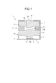
- the imaging unit 1 shown in FIG. 1 includes a sensor module 2 and a lens module 3.
- the sensor module 2 includes a solid-state imaging device 4 and a sensor substrate unit 5.
- the sensor substrate unit 5 is formed of a semiconductor material such as silicon.
- the solid-state imaging device 4 is, for example, a CCD image sensor, a CMOS image sensor, or the like, and repeats a well-known film formation process, photolithography process, etching process, impurity addition process, and the like on the sensor substrate section 5 to thereby form the sensor substrate section 5.
- a light receiving region, an insulating film, an electrode, a wiring, and the like are formed thereon.
- the lens module 3 includes a first lens L1 and a second lens L2.
- the first lens L1 includes a lens portion 16 and a flange portion 17.
- the lens unit 16 has predetermined lens surfaces 16a and 16b on the front and back.
- the lens surfaces 16a and 16b are both convex spherical surfaces in the illustrated example, but various combinations of convex spherical surfaces, concave spherical surfaces, aspherical surfaces, or flat surfaces are adopted depending on the application. obtain.
- the flange portion 17 projects like a bowl from the outer periphery of the lens portion 16 and surrounds the outer periphery of the lens portion 16.
- the lens portion 16 and the flange portion 17 are integrally formed of a translucent material.
- the second lens L2 has the same configuration as the first lens L1. That is, the second lens L ⁇ b> 2 includes a lens part 26 and a flange part 27.
- the lens part 26 has predetermined lens surfaces 26a and 26b on the front and back. Both lens surfaces 26a and 26b are convex spherical surfaces in the illustrated example, but various combinations of convex spherical surfaces, concave spherical surfaces, aspherical surfaces, or flat surfaces are adopted depending on the application. obtain.
- the flange portion 27 protrudes in a bowl shape from the outer periphery of the lens portion 26 and surrounds the outer periphery of the lens portion 26.
- the lens part 26 and the flange part 27 are integrally formed of a translucent material.
- the bonding portion 12 is provided so as to surround the lens surface 16 b of the lens portion 16 and the lens surface 26 a of the lens portion 26. As will be described later, the bonding portion 12 is formed using an ultraviolet curable resin.
- the lens module 3 includes a holding unit 8.
- the holding portion 8 covers the surface of the flange portion 17 of the first lens L1, and has a shape in which a part thereof enters the gap between the flange portion 17 and the flange portion 27.
- the holding part 8 is formed of a light-shielding material.
- the material of the holding part 8 uses a thermosetting resin as will be described later.
- FIG. 2 is a perspective view showing a part of the lens module 3.
- the holding portion 8 has a rectangular body, covers the flange portion 17 excluding the lens surface 16a, and exposes the lens surface 16a to the outside through a substantially circular opening on the upper surface.
- the holding portion 8 may be configured to cover the end face of the flange portion 27 of the second lens L2.
- the lens module 3 holds the first lens L1 and the second lens L2 in a state where the optical axes of the lens portions 16 and 17 are aligned.
- the lens module 3 is laminated on the sensor module 2 via the spacer 9 between the flange portion 27 and the sensor substrate portion 5 and assembled to the sensor module 2.
- the spacer 9 places a predetermined distance between the sensor substrate unit 5 and the flange unit 27 so that the light guided by the lens units 16 and 26 of the lens module 3 is imaged on the light receiving surface of the solid-state imaging device 4. It is thick.
- the spacer 9 and both the modules 2 and 3 are joined using, for example, an adhesive.
- the shape of the spacer 9 is not particularly limited as long as a predetermined distance can be placed between the sensor substrate portion 5 of the sensor module 2 and the flange portion 27 of the lens module 3, but surrounds the solid-state imaging device 4.
- the frame-shaped member is used to isolate the modules 2 and 3 from the outside. According to this, it is possible to prevent foreign matters such as dust from entering between the modules 2 and 3 and adhering to the light receiving surface of the solid-state imaging device 4.
- the spacer 9 is formed of a light-shielding material, unnecessary light incident on the solid-state imaging device 4 from between the modules 2 and 3 can be blocked.
- the lens module 2 includes two lenses L1 and L2, but may include three or more lenses. Further, the plurality of lenses of the lens module may have different shapes.
- the imaging unit 1 configured as described above is reflow-mounted on a circuit board such as a portable terminal.
- Paste solder is printed in advance on the circuit board at a position where the imaging unit 1 is mounted, and the imaging unit 1 is placed there.
- the circuit board including the imaging unit 1 is subjected to heat treatment such as infrared irradiation or hot air blowing. As a result, the solder is melted and the imaging unit 1 is mounted on the circuit board.
- a lens array in which a plurality of lens units 16 are arranged one-dimensionally or two-dimensionally and a lens array in which a plurality of lens units 17 are arranged in the same arrangement as the lens unit 16 are overlapped. It is obtained by cutting the lens array.
- the above-described sensor module 2 is obtained by dividing a sensor array in which a plurality of solid-state image sensors are arranged one-dimensionally or two-dimensionally so as to include individual solid-state image sensors.
- FIG. 3 is a plan view showing the lens array.
- 4 is a cross-sectional view of the lens array shown in FIG. 3 taken along the line IV-IV. 3 and 4, the lens array in which the lens portions 16 are arranged is described as an example, but the configuration of the lens array in which the lens portions 17 are arranged is the same.
- the lens array 100 includes a plurality of lens portions 16 and a substrate portion 101 that integrally connects these lens portions 16.
- the lens array 100 is formed in a wafer shape of a predetermined size as a whole, and a plurality of lens portions 16 are two-dimensionally arranged there, and is also referred to as a wafer level lens array.
- the lens unit 16 and the substrate unit 101 are integrally formed of a translucent material. In the illustrated example, the plurality of lens units 16 may be arranged one-dimensionally.
- the lens array 100 is obtained by molding a resin having optical transparency using a molding die described later.
- the above-described lens module 3 (see FIG. 1) superimposes the lens array 100 and the lens array on which the lens unit 17 is arranged, cuts the substrate unit 101, and separates the lens unit 16 and the lens unit 7 into individual lenses. Can be obtained.
- FIG. 5 is a schematic cross-sectional view for explaining a process of molding the lens array 100. First, the structure of the mold will be described based on FIG. 5A.
- the mold includes a pair of upper and lower molds 120 and 130.
- the mold 120 has a transfer surface 121
- the mold 130 has a transfer surface 131.
- the transfer surface 121 forms the shape of one surface of the lens array 100
- the mold 130 forms the shape of the other surface of the lens array 100.
- the transfer surface 121 has a shape in which one surface of the lens array 10 is inverted, and the transfer surface 31 has a shape in which the other surface of the lens array 10 is inverted.
- a lens molding surface 122 is two-dimensionally arranged on the transfer surface 121 of the mold 120 corresponding to the arrangement of the lens portions 16 of the lens array 100.
- the lens molding surface 122 is molded into a concave spherical surface corresponding to the lens surface 16a which is a convex spherical surface.
- a lens molding surface 132 is two-dimensionally arranged on the transfer surface 131 of the mold 130 corresponding to the arrangement of the lens portions 16 of the lens array 100.
- the lens molding surface 132 is molded into a concave spherical surface corresponding to the lens surface 16a which is a convex spherical surface.
- a resin M which is a material of the lens array 100, is supplied to the transfer surface 131 of the mold 130.
- the resin M is controllably supplied using a supply device such as a dispenser (not shown).
- the material of the resin M is an energy curable resin composition.
- the energy curable resin composition may be either a resin composition that is cured by heat or a resin composition that is cured by irradiation with active energy rays (for example, ultraviolet rays or electron beam irradiation).
- the resin M is deformed following the shape of the transfer surfaces 21 and 31 by being sandwiched between the molds 120 and 130. Thereafter, the resin M sandwiched between the molds 120 and 130 is cured.
- the lens array 100 made of the cured resin M is released from the molds 120 and 130 as shown in FIG. 5C.
- the lens array 100 can be obtained.
- the lens array 200 can also be obtained by a similar procedure.
- the lens array 100 in which the plurality of lens portions 16 are arranged and the 200 in which the plurality of lens portions 17 are arranged are overlapped.
- the lens array 100 and the lens array 200 are bonded to each other by the bonding portion 12.
- the adhesive part 12 is formed using an ultraviolet curable resin.
- the substrate unit 101 and the substrate unit 201 are bonded.
- the adhesive portion 12 is formed so as to surround the lens surface 16b and the lens surface 26a. Further, the adhesive portion 12 partitions the supplied thermosetting resin and the lens portion as will be described later.
- the adhesive portion 12 is formed by forming an ultraviolet curable resin at a predetermined site on the lens array 200, overlaying the lens array 100 and the lens array 200, and curing the ultraviolet curable resin by ultraviolet irradiation.
- the stacked lens arrays 100 and 200 are fixed by being bonded by the bonding portion 12 at a position where the optical axis of the lens portion 16 and the optical axis of the lens portion 26 coincide. In this way, a lens array stacked body is configured by the lens arrays 100 and 200 stacked.
- 7A to 7C show a process for manufacturing a lens module.
- the substrate portion 101 of the lens array 100 is cut with a blade 40 (first cutting portion) such as a dancing blade.
- the cut substrate portion 101 attached to the lens portion 16 becomes the flange portion 17.
- the substrate 101 is cut into a grid shape in a state where the lens array 100 is viewed in plan. Note that only the substrate portion 101 is cut, and the substrate portion 201 of the lens array 200 is not cut.
- thermosetting resin constituting the holding unit 8 is placed in the space between the lens array 100 and the lens array 200 from the gap between the cut surfaces of the substrate unit 101 of the lens array 100.
- the thermosetting resin is supplied by applying it while controlling the supply amount using a dispenser or the like.
- thermosetting resin Since the supplied thermosetting resin is blocked by the adhesive portion 12, it is prevented from adhering to the lens surfaces 16b and 26a. Thus, the thermosetting resin is filled in the space surrounded by the upper surface of the substrate portion 201 of the lens array 200 and the adhesive portion 12 and the substrate portion 101. The thermosetting resin is supplied so as to cover the surface of the flange portion 17 (the surface of the cut substrate portion 101) and the cut surface.
- thermosetting resin After supplying the thermosetting resin, the thermosetting resin is subjected to a heat treatment using a heating means (not shown) to cure the thermosetting resin.
- the substrate portion 201 of the lens array 200 is cut with a blade 60 (second cutting portion) such as a dicing blade, and one lens portion 16 and Each lens module including one lens unit 26 is separated.
- a blade 60 second cutting portion
- the lens module 1 provided with the holding part 8 made of a thermosetting resin can be obtained.
- the thickness of the blade 60 for cutting the substrate portion 201 is thinner than the thickness of the blade 40 for cutting the substrate portion 101. By doing so, it is possible to prevent the thermosetting resin filled in the gap between the cut surfaces of the substrate unit 101 from being removed by the blade 60 when the substrate unit 201 is cut.
- a lens module in which the first lens L1 and the second lens L2 are firmly fixed by the holding portion 8 can be obtained. For this reason, in the reflow process after being mounted on the imaging unit or the like, it is possible to prevent the holding portion 8 from changing the gap between the substrate portions of these lens modules and the optical axis position of the lens portion. Therefore, it can suppress that the optical characteristic of a lens module deteriorates.
- the holding portion 8 is provided not only on the gap between the flange portion 17 of the first lens L1 and the flange portion 27 of the second lens L2, but also on the surface of the flange portion 17 of the first lens L1 and its cut surface.
- the lenses L1 and L2 can be more reliably held as compared with the conventional configuration in which only the gaps between the overlapping lenses are bonded together as in the conventional case.
- the lens module may have a configuration including three or more lenses.
- a method for manufacturing such a lens module as described above, a plurality of lens arrays can be obtained by stacking and separating them with an adhesive portion interposed therebetween.
- the thermosetting resin only the lowermost lens array is used as a base, the substrate portions of other lens arrays are cut with a blade as described above, and the thermosetting resin is formed from the gap between the cut surfaces. Can be supplied. Then, after curing the thermosetting resin, the base lens array may be cut.
- thermosetting resin constituting the holding portion 8 a light-shielding one can be used. In this case, it is not necessary to separately provide a light shielding member for the lens module and the image pickup unit including the lens module.
- thermosetting resin constituting the holding portion 8 a heat-resistant material, for example, a material having a heat resistance of 270 ° C. can be used. If it carries out like this, it can suppress that the retention strength of the holding part 8 of a lens module falls by a reflow process etc., and can hold
- a surface of at least one lens array substrate portion may be provided with a concavo-convex portion that expands a contact area with the filled thermosetting resin.
- the uneven part can be formed on the surface of the substrate part 101 by a mold in the step of forming the lens array.
- a lens module having the structure shown in FIG. 8 can be obtained by manufacturing the lens module by the procedure shown in FIG. 7 using the lens array thus obtained.
- a concave portion 17a is formed in a flange portion 17 formed by cutting a substrate portion of a lens array. Further, the flange portion 27 is formed with a concave portion 27a. If the contact area between the flange portions 17 and 27 and the holding portion 8 is increased as described above, the lenses L1 and L2 can be more reliably held by the holding portion 8.
- the configuration for expanding the contact area between the flange portions 17 and 27 and the holding portion 8 is not limited to the unevenness as shown in FIG. 8, and the cross section may be wavy. Or you may form a fine uneven
- the blade that cuts the substrate portion 101 is a blade having a large abrasive grain size, and the cut surface of the substrate portion is made rough, thereby supplying heat to the rough surface. Adhesive strength with the curable resin can be increased.
- a lens module manufacturing method for holding a plurality of lenses by aligning the optical axes of the lenses and including a lens array having a plurality of lens portions and a substrate portion integrally connecting the plurality of lens portions, A plurality of lens arrays are stacked at a predetermined interval so that the optical axes of the lens portions between the overlapping lens arrays coincide with each other, and a lens array substrate other than the lowermost lens array in the overlapping direction among the stacked lens arrays.
- the portion is cut by the first cutting portion, the thermosetting resin is supplied from the gap between the cut surfaces of the cut substrate portions, and the thermosetting resin is filled in the gap between the substrate portions between the overlapping lens arrays.
- thermosetting resin integrally covers the cut surface of the substrate part and the surface of the substrate part of the uppermost lens array in the overlapping direction among the multiple lens arrays to be overlaid, Then, heat is supplied to the thermosetting resin to cure it, and the substrate part of the lens array that is the lowest in the overlapping direction among the multiple lens arrays to be stacked is cut at the second cutting part and separated into lens modules.
- a method for manufacturing a lens module. (2) A manufacturing method of the lens module according to (1), A method for manufacturing a lens module, wherein an uneven portion that expands a contact area with a thermosetting resin to be filled is provided on a surface of a substrate portion of at least one lens array among the overlapping lens arrays.
- the thermosetting resin is a material having heat resistance.
Landscapes
- Physics & Mathematics (AREA)
- General Physics & Mathematics (AREA)
- Optics & Photonics (AREA)
- Engineering & Computer Science (AREA)
- Health & Medical Sciences (AREA)
- Manufacturing & Machinery (AREA)
- Ophthalmology & Optometry (AREA)
- Mechanical Engineering (AREA)
- Solid State Image Pick-Up Elements (AREA)
- Lens Barrels (AREA)
- Transforming Light Signals Into Electric Signals (AREA)
Abstract
光学特性の劣化を抑えることができるレンズモジュールの製造方法、及びレンズモジュールを提供する。複数のレンズ部と複数のレンズ部を一体に繋げる基板部とを有するレンズアレイを、所定の間隔をおいて複数個重ねて、重ね合うレンズアレイ間のレンズ部の光軸を一致させ、重ねられる複数のレンズアレイのうち重なり合う方向において最も下方のレンズアレイを除いた他のレンズアレイの基板部を第1の切断部によって切断し、切断された基板部の隙間から熱硬化性樹脂を供給し、熱硬化性樹脂を重なり合うレンズアレイ間の基板部同士の隙間に充填するとともに、該熱硬化性樹脂によって基板部の切断面及び最も上方のレンズアレイの基板部の表面を一体覆い、その後、熱硬化性樹脂に熱を供給して硬化させ、最も下方のレンズアレイの基板部を第2の切断部で切断してレンズモジュールごとに分離する。
Description
本発明は、レンズモジュールの製造方法、及びレンズモジュールに関する。
近年、携帯電話やPDA(Personal Digital Assistant)などの携帯端末には、小型で薄型な撮像ユニットが搭載されている。このような撮像ユニットは、一般に、CCD(Charge Coupled Device)イメージセンサやCMOS(Complementary Metal-Oxide Semiconductor)イメージセンサなどの固体撮像素子と、固体撮像素子上に被写体像を形成するためのレンズと、を備えている。
撮像ユニットのコストの低下を図るため、撮像ユニットに実装されるレンズを大量にかつ安価に製造できるように、レンズの製造方法を効率化することが望まれている。このようなレンズは、基板部に複数のレンズ部を一体に形成した構成であるレンズアレイを製造し、該基板部を切断して複数のレンズ部をそれぞれ分離させることで得られ、その後、撮像ユニットに実装される。
特許文献1には、基板部と複数のレンズ部とが一体に形成されたウエハレベルレンズアレイを、別のウエハレベルレンズアレイに接着材で貼り合わせるレンズモジュールの製造方法が記載されている。
貼り合わされたレンズモジュールを基板部で切断して、撮像ユニットに実装される。撮像ユニットは、例えば携帯端末等の回路基板にリフロー実装される。
しかし、上述した特許文献1のように接着剤による接着では、レンズモジュールを撮像ユニットに実装させた後のリフロー工程等において、これらレンズモジュールの基板部同士の隙間や、レンズ部の光軸位置が変わることにより、レンズモジュールの光学特性が劣化する。
本発明は、上記事情を鑑みてなされたものであり、光学特性の劣化を抑えることができるレンズモジュールの製造方法、及びレンズモジュールを提供する。
(1)複数のレンズを、各レンズの光軸が一致するように保持するレンズモジュールの製造方法であって、複数のレンズ部と複数のレンズ部を一体に繋げる基板部とを有するレンズアレイを、所定の間隔をとって複数個重ねて、重ね合うレンズアレイ間のレンズ部の光軸を一致させ、重ねられる複数のレンズアレイのうち重なり合う方向に最も下方のレンズアレイを除いた他のレンズアレイの基板部を第1の切断部によって切断し、切断された基板部の切断面同士の隙間から熱硬化性樹脂を供給し、重なり合うレンズアレイ間の基板部同士の隙間に熱硬化性樹脂を充填するとともに、熱硬化性樹脂によって基板部の切断面及び、重ねられる複数のレンズアレイのうち重なり合う方向に最も上方のレンズアレイの基板部の表面を一体覆い、その後、熱硬化性樹脂に熱を供給して硬化させ、重ねられる複数の前記レンズアレイのうち重なり合う方向に最も下方のレンズアレイの基板部を第2の切断部で切断してレンズモジュールごとに分離する、レンズモジュールの製造方法。
(2)(1)のレンズモジュールの製造方法によって製造されるレンズモジュール。ここで、重なり合う方向に最も上方のレンズアレイとは、重なり合う方向のうち重力の働く方向と反対側に向かって最も上にあるレンズアレイを言い、重なり合う方向に最も下方のレンズアレイとは、重なり合う方向のうち重力の働く方向に向かって最も下にあるレンズアレイを言うものである。また、レンズアレイの基板部の表面とは、レンズアレイに形成された複数のレンズ部の光軸方向に略垂直な2つの面を言うものである。
(2)(1)のレンズモジュールの製造方法によって製造されるレンズモジュール。ここで、重なり合う方向に最も上方のレンズアレイとは、重なり合う方向のうち重力の働く方向と反対側に向かって最も上にあるレンズアレイを言い、重なり合う方向に最も下方のレンズアレイとは、重なり合う方向のうち重力の働く方向に向かって最も下にあるレンズアレイを言うものである。また、レンズアレイの基板部の表面とは、レンズアレイに形成された複数のレンズ部の光軸方向に略垂直な2つの面を言うものである。
本発明によれば、光学特性の劣化を抑えることができるレンズモジュールの製造方法、及びレンズモジュールを提供できる。
図1に示す撮像ユニット1は、センサモジュール2と、レンズモジュール3と、を備えている。
センサモジュール2は、固体撮像素子4と、センサ基板部5とを備えている。センサ基板部5は、例えばシリコンなどの半導体材料で形成されている。固体撮像素子4は、例えばCCDイメージセンサやCMOSイメージセンサなどであり、センサ基板部5に対して周知の成膜工程、フォトリソグラフィー工程、エッチング工程、不純物添加工程、等を繰り返し、センサ基板部5上に受光領域、絶縁膜、電極、配線、等を形成して構成されている。
レンズモジュール3は、第1のレンズL1と第2のレンズL2とを備える。
第1のレンズL1は、レンズ部16と、フランジ部17とを備えている。レンズ部16は、その表裏に所定のレンズ面16a、16bを有している。両レンズ面16a、16bは、図示の例ではいずれも凸形状の球面とされているが、用途に応じて、凸形状の球面、凹形状の球面、非球面、又は平面の種々の組み合わせを採り得る。フランジ部17は、レンズ部16の外周から鍔状に張り出して、レンズ部16の外周を取り囲んでいる。レンズ部16、及びフランジ部17は、透光性の材料で一体に形成されている。
第2のレンズL2は、第1のレンズL1と同様の構成である。すなわち、第2のレンズL2は、レンズ部26と、フランジ部27とを備える。レンズ部26は、その表裏に所定のレンズ面26a、26bを有している。両レンズ面26a、26bは、図示の例ではいずれも凸形状の球面とされているが、用途に応じて、凸形状の球面、凹形状の球面、非球面、又は平面の種々の組み合わせを採り得る。フランジ部27は、レンズ部26の外周から鍔状に張り出して、レンズ部26の外周を取り囲んでいる。レンズ部26、及びフランジ部27は、透光性の材料で一体に形成されている。
第1のレンズL1と第2のレンズL2との間には、両者の位置を互い固定するための接着部12が設けられている。接着部12は、レンズ部16のレンズ面16bとレンズ部26のレンズ面26aの周囲を囲って設けられている。接着部12は、後述するように、紫外線硬化樹脂を用いて形成される。
また、レンズモジュール3は、保持部8を備える。
保持部8は、第1のレンズL1のフランジ部17の表面を覆い、その一部がフランジ部17とフランジ部27との隙間に入り込んだ形状を有する。保持部8は、遮光性を有する材料で形成されている。保持部8の材料は、後述するように、熱硬化性樹脂を用いる。
図2は、レンズモジュール3の一部を示す斜視図である。保持部8は、矩形体を有し、レンズ面16aを除くフランジ部17を覆い、上面の略円形の開口からレンズ面16aを外部に露呈する。
なお、保持部8は、第2のレンズL2のフランジ部27の端面を覆う構成としてもよい。
図1に示すように、レンズモジュール3は、レンズ部16,17の光軸を一致させた状態で、第1のレンズL1と第2のレンズL2を重ねて保持する。
レンズモジュール3は、そのフランジ部27とセンサ基板部5との間にスペーサ9を介してセンサモジュール2に積層され、センサモジュール2に組み付けられる。スペーサ9は、レンズモジュール3のレンズ部16,26で導かれた光を固体撮像素子4の受光面に結像するように、センサ基板部5とフランジ部27との間に所定の距離を置く厚みとなっている。スペーサ9と両モジュール2、3とは、例えば接着剤などを用いて接合される。
スペーサ9は、センサモジュール2のセンサ基板部5とレンズモジュール3のフランジ部27との間に所定の距離を置くことができる限り、その形状は特に限定されないが、固体撮像素子4の周囲を取り囲んで両モジュール2、3の間を外より隔絶する枠状の部材であることが好ましい。これによれば、両モジュール2、3の間から塵等の異物が入り、それが固体撮像素子4の受光面に付着することを防止することができる。更に、スペーサ9を遮光性の材料で形成すれば、両モジュール2、3の間から固体撮像素子4に入射する不要な光を遮ることができる。
なお、レンズモジュール2は2個のレンズL1,L2を有するが、3個以上のレンズを有していてもよい。また、レンズモジュールの複数のレンズはそれぞれ、異なる形状であってもよい。
以上のように構成された撮像ユニット1は、例えば携帯端末等の回路基板にリフロー実装される。回路基板には撮像ユニット1が実装される位置に予めペースト状の半田が印刷されており、そこに撮像ユニット1が載置される。そして、撮像ユニット1を含む回路基板に赤外線の照射や熱風の吹付けといった加熱処理が施される。それにより半田が溶け、撮像ユニット1は回路基板に実装される。
上述のレンズモジュール3は、複数のレンズ部16が1次元又は2次元に配列されたレンズアレイと、複数のレンズ部17がレンズ部16と同じ配置で配列されたレンズアレイとを重ねて、重ねられたレンズアレイを切断して得られる。また、上述のセンサモジュール2も同様に、複数の固体撮像素子が1次元又は2次元に配列されたセンサアレイを、個々に固体撮像素子を含むように分断して得られる。以下に、レンズモジュール3を製造するために使用されるレンズアレイの構成について説明する。
図3は、レンズアレイを示す平面図である。図4は、図3に示すレンズアレイのIV-IV線断面図である。図3及び図4では、レンズ部16が配列されたレンズアレイを例に説明しているが、レンズ部17が配列されたレンズアレイの構成についても同じである。
レンズアレイ100は、複数のレンズ部16と、これらのレンズ部16を一体に繋ぐ基板部101とを備えている。このレンズアレイ100は、全体として所定のサイズのウエハ状をなし、そこに複数のレンズ部16が2次元に配列されたものであり、ウエハレベルレンズアレイとも称される。これらのレンズ部16、及び基板部101は、透光性の材料で一体に形成されている。なお、図示の例では、複数のレンズ部16は1次元に配列されていてもよい。
レンズアレイ100は、後述する成形型を用いて光透過性を有する樹脂を成形することで得られる。
上述のレンズモジュール3(図1参照)は、レンズアレイ100と、レンズ部17が配列されたレンズアレイとを重ね合わせ、基板部101を切断して個別のレンズ部16及びレンズ部7に分離することで得られる。
次に、図3及び4に示すレンズアレイ100を成形する手順を説明する。
図5は、レンズアレイ100を成形する工程を説明するための模式的な断面図である。はじめに、図5Aに基づいて、成形型の構成を説明する。
成形型は、上下一対の型120,130を備える。型120は、転写面121を有し、型130は、転写面131を有する。型120は、転写面121がレンズアレイ100の一方の面の形状を成形するものであり、型130は、レンズアレイ100の他方の面の形状を成形するものである。
転写面121は、レンズアレイ10の一方の面を反転させた形状であり、転写面31は、レンズアレイ10の他方の面を反転させた形状である。
型120の転写面121には、レンズアレイ100のレンズ部16の配列に対応してレンズ成形面122が2次元に配列されている。レンズ成形面122は、凸形状の球面であるレンズ面16aに対応して凹形状の球面に成形されている。
型130の転写面131には、レンズアレイ100のレンズ部16の配列に対応してレンズ成形面132が2次元に配列されている。レンズ成形面132は、凸形状の球面であるレンズ面16aに対応して凹形状の球面に成形されている。
次に、上述の成形型を用いた製造方法の手順を説明する。
最初に、図5Aに示すように、型130の転写面131にレンズアレイ100の材料である樹脂Mを供給する。樹脂Mは、図示しないディスペンサなどの供給装置を用いて制御可能に供給される。
樹脂Mの材料は、エネルギー硬化性の樹脂組成物が用いられる。エネルギー硬化性の樹脂組成物は、熱により硬化する樹脂組成物、あるいは活性エネルギー線の照射(例えば紫外線、電子線照射)により硬化する樹脂組成物のいずれであってもよい。
図5Bに示すように型120,130で挟み込むことで、樹脂Mを転写面21,31の形状に倣って変形する。その後、型120,130で挟み込まれた樹脂Mを硬化させる。
樹脂の硬化後に、図5Cに示すように、硬化された樹脂Mからなるレンズアレイ100を、型120,130から離型する。こうしてレンズアレイ100を得ることができる。レンズアレイ200も同様の手順によって得ることができる。
次に、図6及び図7に基づいて、上述のレンズモジュールを製造する手順を説明する。
図6に示すように、複数のレンズ部16が配列されたレンズアレイ100と、複数のレンズ部17が配列された200とを重ねる。レンズアレイ100とレンズアレイ200とは接着部12によって互いに接着される。
図6に示すように、複数のレンズ部16が配列されたレンズアレイ100と、複数のレンズ部17が配列された200とを重ねる。レンズアレイ100とレンズアレイ200とは接着部12によって互いに接着される。
接着部12は、紫外線硬化性樹脂を用いて形成される。基板部101と基板部201とを接着する。
また、接着部12は、レンズ面16b及びレンズ面26aの周囲を囲うように形成されている。更に、接着部12は、後述するように、供給される熱硬化性樹脂とレンズ部とを仕切る。
接着部12の形成は、紫外線硬化性樹脂をレンズアレイ200上の所定の部位に形成し、レンズアレイ100とレンズアレイ200とを重ね合わせ、紫外線照射により紫外線硬化樹脂を硬化させることによってなされる。
本発明において、重ねられたレンズアレイ100,200は、レンズ部16の光軸とレンズ部26の光軸とが一致する位置で、接着部12によって接着されることにより、固定されている。こうして、重ねられたレンズアレイ100,200によってレンズアレイ積層体が構成される。
次に、上述のレンズアレイ積層体からレンズモジュールを製造する手順を説明する。
図7Aから図7Cは、レンズモジュールを製造する工程を示している。
図7Aに示すように、レンズアレイ100の基板部101を、ダンシングブレード等の刃40(第1の切断部)で切断する。レンズ部16に付属する切断された基板部101がフランジ部17となる。ここで、レンズアレイ100を平面視した状態で、基板部101を升目状に切断する。なお、基板部101のみを切断し、レンズアレイ200の基板部201は切断しない。
次に、図7Bに示すように、レンズアレイ100の基板部101における切断面同士の隙間から、保持部8を構成する熱硬化性樹脂を、レンズアレイ100及びレンズアレイ200との間の空間に供給する。熱硬化性樹脂の供給はディスペンサ等を用いて供給量を制御しつつ塗布することで行われる。
供給された熱硬化性樹脂は、接着部12に遮られるため、レンズ面16b,26aに付着することが防止される。こうして、熱硬化性樹脂は、レンズアレイ200の基板部201の上面と、接着部12と基板部101とに囲われた空間に充填される。また、熱硬化性樹脂は、フランジ部17の表面(切断された基板部101の表面)及びその切断面を覆うように供給される。
熱硬化性樹脂を供給した後、熱硬化性樹脂に図示しない加熱手段を用いて加熱処理を行い、熱硬化性樹脂を硬化させる。
熱硬化性樹脂を硬化させた後、図7Cに示すように、レンズアレイ200の基板部201をダイシングブレード等の刃60(第2の切断部)で切断して、1個のレンズ部16と1個のレンズ部26とを含むレンズモジュールごとに分離する。こうして、熱硬化性樹脂からなる保持部8を備えたレンズモジュール1を得ることができる。
ここで、基板部101を切断する刃40の厚みより、基板部201を切断する刃60の厚みが薄いことが好ましい。こうすれば、基板部101の切断面同士の隙間に充填した熱硬化性樹脂が基板部201の切断時に刃60によって取り除かれてしまうことを抑えることができる。
上述したレンズモジュールの製造方法によれば、第1のレンズL1と第2のレンズL2とを保持部8によって強固に固定したレンズモジュールを得ることができる。このため、撮像ユニットに実装させた後のリフロー工程等において、保持部8によってこれらレンズモジュールの基板部同士の隙間やレンズ部の光軸位置が変わることが抑えられる。よって、レンズモジュールの光学特性が劣化することを抑えることができる。
また、保持部8は、第1のレンズL1のフランジ部17と第2のレンズL2のフランジ部27との隙間だけでなく、第1のレンズL1のフランジ部17の表面とその切断面にも一体に形成されており、従来のように重なったレンズ同士の隙間のみを接着した構成に比べて、各レンズL1,L2同士をより確実に保持することができる。
次に、本発明のレンズモジュールの構成の変形例を説明する。
レンズモジュールは、3個以上のレンズを備えた構成としてもよい。このようなレンズモジュールを製造する方法としては、上述したように複数のレンズアレイを接着部を挟んで重ねて分離させて得ることができる。熱硬化性樹脂を供給する際には、最も下方のレンズアレイのみをベースとして、他の複数のレンズアレイの基板部を上述したように刃で切断し、切断面同士の隙間から熱硬化性樹脂を供給すればよい。その後、熱硬化性樹脂を硬化させた後、ベースとしたレンズアレイを切断すればよい。
保持部8を構成する熱硬化性樹脂は、遮光性のものを用いることができる。こうすれば、レンズモジュール及びこのレンズモジュールを備えた撮像ユニットに別途、遮光部材を備え付ける必要がない。
保持部8を構成する熱硬化性樹脂は、耐熱性を有する材料、例えば、270℃の耐熱性を有する材料を用いることができる。こうすれば、リフロー工程等でレンズモジュールの保持部8の保持力が低下することを抑えられ、レンズをより確実に保持することができる。
重なり合うレンズアレイの基板部のうち、少なくとも1つのレンズアレイの基板部の表面に、充填される熱硬化性樹脂との接触面積を拡げる凹凸部が設けられていてもよい。凹凸部は、レンズアレイを成形する工程において、型によって基板部101の表面に形成することができる。このように得られたレンズアレイを用いて図7に示す手順によってレンズモジュールを製造することで、図8に示すように構成のレンズモジュールを得ることができる。
図8に示すレンズモジュール3は、レンズアレイの基板部を切断してなるフランジ部17に凹部17aが形成されている。また、フランジ部27には凹部27aが形成されている。このようにフランジ部17,27と保持部8との接触面積を拡げる構成とすれば、保持部8によってレンズL1,L2をより確実に保持させることができる。
フランジ部17,27と保持部8との接触面積を拡げる構成としては、図8に示すような凹凸に限らず、断面が波状のものとしてもよい。又は、フランジ部17,27の表面に微細な凹凸パターンを形成してもよい。
図7Aに示す工程において、基板部101を切断する刃として、砥粒径が大きいサイズのものを用いることで、基板部の切断面を粗面とすることで、該粗面と供給される熱硬化性樹脂との密着力を大きくすることができる。
本明細書は以下の内容を開示する。
(1)複数のレンズを、各レンズの光軸を一致させて保持するレンズモジュールの製造方法であって、複数のレンズ部と複数のレンズ部を一体に繋げる基板部とを有するレンズアレイを、所定の間隔をとって複数個重ねて、重ね合うレンズアレイ間のレンズ部の光軸を一致させ、重ねられる複数のレンズアレイのうち重なり合う方向において最も下方のレンズアレイを除いた他のレンズアレイの基板部を第1の切断部によって切断し、切断された基板部の切断面同士の隙間から熱硬化性樹脂を供給し、重なり合うレンズアレイ間の基板部同士の隙間に熱硬化性樹脂を充填するとともに、該熱硬化性樹脂によって基板部の切断面及び、重ねられる複数のレンズアレイのうち重なり合う方向に最も上方のレンズアレイの基板部の表面を一体覆い、その後、熱硬化性樹脂に熱を供給して硬化させ、重ねられる複数のレンズアレイのうち重なり合う方向に最も下方のレンズアレイの基板部を第2の切断部で切断してレンズモジュールごとに分離する、レンズモジュールの製造方法。
(2)(1)に記載のレンズモジュールの製造方法であって、
重なり合うレンズアレイのうち、少なくとも1つのレンズアレイの基板部の表面に、充填される熱硬化性樹脂との接触面積を拡げる凹凸部が設けられているレンズモジュールの製造方法。
(3)(1)又は(2)に記載のレンズモジュールの製造方法であって、基板部を第1の切断部によって切断するときに、該基板部における切断面に粗面を形成するレンズモジュールの製造方法。
(4)(1)から(3)のいずれか1つに記載のレンズモジュールの製造方法であって、レンズアレイを複数個重ねる際に、重ねられる複数のレンズアレイ同士を接着部によって接着するレンズモジュールの製造方法。
(5)(4)に記載のレンズモジュールの製造方法であって、
接着部をレンズ部の周囲に形成し、該接着部によって供給される熱硬化性樹脂とレンズ部とを仕切るレンズモジュールの製造方法。
(6)(4)又は(5)に記載のレンズモジュールの製造方法であって、
接着部は紫外線硬化性樹脂であって、基板部を切断する前に、紫外線硬化性樹脂を硬化させることで、重ねられたレンズアレイ同士を固定するレンズモジュールの製造方法。
(7)(1)から(6)のいずれか1つに記載のレンズモジュールの製造方法であって、第1の切断部及び第2の切断部はそれぞれ刃を備え、第2の切断部の刃が第1の切断部の刃より厚みが薄いレンズモジュールの製造方法。
(8)(1)から(7)のいずれか1つに記載のレンズモジュールの製造方法であって、熱硬化性樹脂は耐熱性を有する材料であるレンズモジュールの製造方法。
(9)(1)から(8)のいずれか1つに記載のレンズモジュールの製造方法であって、熱硬化性樹脂は遮光性を有する材料であるレンズモジュールの製造方法。
(10)(1)から(9)のいずれか1つに記載のレンズモジュールの製造方法によって製造されるレンズモジュール。
1 撮像ユニット
2 センサモジュール
3 レンズモジュール
8 保持部
16,26 レンズ部
17,27 フランジ部
100 レンズアレイ
101 基板部
120,130 成形型
L1,L2 レンズ
2 センサモジュール
3 レンズモジュール
8 保持部
16,26 レンズ部
17,27 フランジ部
100 レンズアレイ
101 基板部
120,130 成形型
L1,L2 レンズ
Claims (11)
- 複数のレンズを、各レンズの光軸を一致させて保持するレンズモジュールの製造方法であって、
複数のレンズ部と前記複数のレンズ部を一体に繋げる基板部とを有するレンズアレイを、所定の間隔をとって複数個重ねて、重ね合うレンズアレイ間の前記レンズ部の光軸を一致させ、
重ねられる複数の前記レンズアレイのうち重なり合う方向に最も下方のレンズアレイを除いた他のレンズアレイの前記基板部を第1の切断部によって切断し、
切断された前記基板部の切断面同士の隙間から熱硬化性樹脂を供給し、重なり合うレンズアレイ間の前記基板部同士の隙間に前記熱硬化性樹脂を充填するとともに、該熱硬化性樹脂によって前記基板部の切断面及び、重ねられる複数の前記レンズアレイのうち重なり合う方向に最も上方のレンズアレイの前記基板部の表面を一体に覆い、
前記熱硬化性樹脂に熱を供給して硬化させ、
前記最も下方のレンズアレイの前記基板部を第2の切断部で切断して前記レンズモジュールごとに分離する、レンズモジュールの製造方法。 - 請求項1に記載のレンズモジュールの製造方法であって、
重なり合うレンズアレイのうち、少なくとも1つの前記レンズアレイの前記基板部の表面に、充填される前記熱硬化性樹脂との接触面積を拡げる凹凸部を設けるレンズモジュールの製造方法。 - 請求項1又は2に記載のレンズモジュールの製造方法であって、
前記基板部を前記第1の切断部によって切断するときに、該基板部における切断面に粗面を形成するレンズモジュールの製造方法。 - 請求項1から3のいずれか1項に記載のレンズモジュールの製造方法であって、
前記レンズアレイを複数個重ねる際に、重ねられる複数の前記レンズアレイ同士を接着部によって接着するレンズモジュールの製造方法。 - 請求項4に記載のレンズモジュールの製造方法であって、
前記接着部を前記レンズ部の周囲に形成し、該接着部によって供給される前記熱硬化性樹脂と前記レンズ部とを仕切るレンズモジュールの製造方法。 - 請求項4又は5に記載のレンズモジュールの製造方法であって、
前記接着部は紫外線硬化性樹脂であって、前記基板部を切断する前に、前記紫外線硬化性樹脂を硬化させることで、重ねられた前記レンズアレイ同士を固定するレンズモジュールの製造方法。 - 請求項1から6のいずれか1項に記載のレンズモジュールの製造方法であって、
前記第1の切断部及び前記第2の切断部はそれぞれ刃を備え、前記第2の切断部の刃が前記第1の切断部の刃より厚みが薄いレンズモジュールの製造方法。 - 請求項1から7のいずれか1項に記載のレンズモジュールの製造方法であって、
前記熱硬化性樹脂は耐熱性を有する材料であるレンズモジュールの製造方法。 - 請求項1から8のいずれか1項に記載のレンズモジュールの製造方法であって、
前記熱硬化性樹脂は遮光性を有する材料であるレンズモジュールの製造方法。 - 請求項1から9のいずれか1項に記載のレンズモジュールの製造方法によって製造されるレンズモジュール。
- 固体撮像素子及びセンサ基板部を有するセンサモジュール、並びに、請求項10に記載のレンズモジュールを備える撮像ユニット。
Priority Applications (4)
| Application Number | Priority Date | Filing Date | Title |
|---|---|---|---|
| CN201280010465.4A CN103392141B (zh) | 2011-03-01 | 2012-02-27 | 透镜模块的制造方法及透镜模块 |
| EP12752308.2A EP2682797B1 (en) | 2011-03-01 | 2012-02-27 | Method for manufacturing lens module, and lens module |
| JP2013502299A JP5401628B2 (ja) | 2011-03-01 | 2012-02-27 | レンズモジュールの製造方法、及びレンズモジュール |
| US14/013,659 US8711483B2 (en) | 2011-03-01 | 2013-08-29 | Lens module and method for manufacturing thereof |
Applications Claiming Priority (2)
| Application Number | Priority Date | Filing Date | Title |
|---|---|---|---|
| JP2011044549 | 2011-03-01 | ||
| JP2011-044549 | 2011-03-01 |
Related Child Applications (1)
| Application Number | Title | Priority Date | Filing Date |
|---|---|---|---|
| US14/013,659 Continuation US8711483B2 (en) | 2011-03-01 | 2013-08-29 | Lens module and method for manufacturing thereof |
Publications (1)
| Publication Number | Publication Date |
|---|---|
| WO2012117986A1 true WO2012117986A1 (ja) | 2012-09-07 |
Family
ID=46757920
Family Applications (1)
| Application Number | Title | Priority Date | Filing Date |
|---|---|---|---|
| PCT/JP2012/054692 WO2012117986A1 (ja) | 2011-03-01 | 2012-02-27 | レンズモジュールの製造方法、及びレンズモジュール |
Country Status (5)
| Country | Link |
|---|---|
| US (1) | US8711483B2 (ja) |
| EP (1) | EP2682797B1 (ja) |
| JP (1) | JP5401628B2 (ja) |
| CN (1) | CN103392141B (ja) |
| WO (1) | WO2012117986A1 (ja) |
Cited By (8)
| Publication number | Priority date | Publication date | Assignee | Title |
|---|---|---|---|---|
| KR20150110657A (ko) * | 2013-01-23 | 2015-10-02 | 뉴바이오 테라퓨틱스, 아이엔씨. | 세자리 코넥손 및 그의 용도 |
| JP2016506326A (ja) * | 2012-12-27 | 2016-03-03 | ヘプタゴン・マイクロ・オプティクス・プライベート・リミテッドHeptagon Micro Optics Pte. Ltd. | 光学素子の製造およびそれを組込んだモジュール |
| CN105814362A (zh) * | 2013-10-07 | 2016-07-27 | Lg伊诺特有限公司 | 透镜模块以及包括该透镜模块的发光装置封装件 |
| WO2017203592A1 (ja) * | 2016-05-24 | 2017-11-30 | オリンパス株式会社 | 内視鏡用光学ユニット、内視鏡、および内視鏡用光学ユニットの製造方法 |
| WO2017203593A1 (ja) * | 2016-05-24 | 2017-11-30 | オリンパス株式会社 | 内視鏡用光学ユニットの製造方法、内視鏡用光学ユニット、および内視鏡 |
| WO2020084728A1 (ja) * | 2018-10-25 | 2020-04-30 | オリンパス株式会社 | 内視鏡レンズユニット、内視鏡、および、内視鏡レンズユニットの製造方法 |
| WO2020230261A1 (ja) * | 2019-05-14 | 2020-11-19 | オリンパス株式会社 | 内視鏡用撮像装置の製造方法、内視鏡用撮像装置、および内視鏡 |
| WO2021033623A1 (ja) * | 2019-08-20 | 2021-02-25 | Agc株式会社 | 光学素子、光学ユニット及び光学素子の製造方法 |
Families Citing this family (6)
| Publication number | Priority date | Publication date | Assignee | Title |
|---|---|---|---|---|
| US9386203B2 (en) * | 2013-10-28 | 2016-07-05 | Omnivision Technologies, Inc. | Compact spacer in multi-lens array module |
| KR101619504B1 (ko) * | 2014-03-20 | 2016-05-10 | (주) 굿피앤씨 | Led 조명 광학계 모듈 및 이를 구비하는 노광 공정용 광원 |
| US10371954B2 (en) | 2014-06-10 | 2019-08-06 | Ams Sensors Singapore Pte. Ltd. | Optoelectronic modules including hybrid arrangements of beam shaping elements, and imaging devices incorporating the same |
| TWI741988B (zh) * | 2015-07-31 | 2021-10-11 | 日商新力股份有限公司 | 堆疊式透鏡結構及其製造方法,以及電子裝置 |
| JP6851838B2 (ja) | 2017-01-26 | 2021-03-31 | ソニーセミコンダクタソリューションズ株式会社 | 積層レンズ構造体、カメラモジュール、および、電子機器 |
| JP2021153780A (ja) * | 2020-03-26 | 2021-10-07 | 株式会社フジクラ | 内視鏡 |
Citations (4)
| Publication number | Priority date | Publication date | Assignee | Title |
|---|---|---|---|---|
| JP2009086092A (ja) * | 2007-09-28 | 2009-04-23 | Aji Kk | 光学部品の製造方法及び撮影装置の製造方法 |
| JP2009251249A (ja) | 2008-04-04 | 2009-10-29 | Sharp Corp | ウエハ状光学装置およびその製造方法、電子素子ウエハモジュール、センサウエハモジュール、電子素子モジュール、センサモジュール、電子情報機器 |
| JP2010204632A (ja) * | 2009-02-06 | 2010-09-16 | Fujifilm Corp | ウェハレベルレンズアレイの製造方法、ウェハレンズアレイ、レンズモジュール及び撮像ユニット |
| JP2010256563A (ja) * | 2009-04-23 | 2010-11-11 | Sharp Corp | レンズアレイおよび当該レンズアレイの製造方法、並びに、その利用 |
Family Cites Families (7)
| Publication number | Priority date | Publication date | Assignee | Title |
|---|---|---|---|---|
| CN100454070C (zh) * | 2005-09-02 | 2009-01-21 | 亚洲光学股份有限公司 | 微型镜头及其制造方法 |
| JP4871690B2 (ja) * | 2006-09-28 | 2012-02-08 | 富士フイルム株式会社 | 固体撮像装置の製造方法及び固体撮像装置 |
| JP2010532492A (ja) * | 2007-07-03 | 2010-10-07 | オプトメカ コーポレイション リミテッド | 異なる素材からなるレンズユニット及びこれを備えるカメラモジュール、並びにその製造方法 |
| JP4966931B2 (ja) * | 2008-08-26 | 2012-07-04 | シャープ株式会社 | 電子素子ウエハモジュールおよびその製造方法、電子素子モジュールおよびその製造方法、電子情報機器 |
| US20100284089A1 (en) * | 2009-05-07 | 2010-11-11 | San-Woei Shyu | Stacked optical glass lens array, stacked lens module and manufacturing method thereof |
| JP5254139B2 (ja) * | 2009-07-03 | 2013-08-07 | シャープ株式会社 | 多層レンズ、積層型ウェハレンズおよびその製造方法 |
| JP5352392B2 (ja) * | 2009-09-14 | 2013-11-27 | 富士フイルム株式会社 | ウェハレベルレンズアレイの製造方法、ウェハレベルレンズアレイ、レンズモジュール及び撮像ユニット |
-
2012
- 2012-02-27 EP EP12752308.2A patent/EP2682797B1/en not_active Not-in-force
- 2012-02-27 JP JP2013502299A patent/JP5401628B2/ja not_active Expired - Fee Related
- 2012-02-27 CN CN201280010465.4A patent/CN103392141B/zh not_active Expired - Fee Related
- 2012-02-27 WO PCT/JP2012/054692 patent/WO2012117986A1/ja active Application Filing
-
2013
- 2013-08-29 US US14/013,659 patent/US8711483B2/en not_active Expired - Fee Related
Patent Citations (4)
| Publication number | Priority date | Publication date | Assignee | Title |
|---|---|---|---|---|
| JP2009086092A (ja) * | 2007-09-28 | 2009-04-23 | Aji Kk | 光学部品の製造方法及び撮影装置の製造方法 |
| JP2009251249A (ja) | 2008-04-04 | 2009-10-29 | Sharp Corp | ウエハ状光学装置およびその製造方法、電子素子ウエハモジュール、センサウエハモジュール、電子素子モジュール、センサモジュール、電子情報機器 |
| JP2010204632A (ja) * | 2009-02-06 | 2010-09-16 | Fujifilm Corp | ウェハレベルレンズアレイの製造方法、ウェハレンズアレイ、レンズモジュール及び撮像ユニット |
| JP2010256563A (ja) * | 2009-04-23 | 2010-11-11 | Sharp Corp | レンズアレイおよび当該レンズアレイの製造方法、並びに、その利用 |
Non-Patent Citations (1)
| Title |
|---|
| See also references of EP2682797A4 |
Cited By (16)
| Publication number | Priority date | Publication date | Assignee | Title |
|---|---|---|---|---|
| JP2016506326A (ja) * | 2012-12-27 | 2016-03-03 | ヘプタゴン・マイクロ・オプティクス・プライベート・リミテッドHeptagon Micro Optics Pte. Ltd. | 光学素子の製造およびそれを組込んだモジュール |
| KR20150110657A (ko) * | 2013-01-23 | 2015-10-02 | 뉴바이오 테라퓨틱스, 아이엔씨. | 세자리 코넥손 및 그의 용도 |
| KR102076219B1 (ko) | 2013-01-23 | 2020-02-11 | 뉴바이오 테라퓨틱스, 아이엔씨. | 세자리 코넥손 및 그의 용도 |
| CN105814362A (zh) * | 2013-10-07 | 2016-07-27 | Lg伊诺特有限公司 | 透镜模块以及包括该透镜模块的发光装置封装件 |
| CN105814362B (zh) * | 2013-10-07 | 2020-03-10 | Lg伊诺特有限公司 | 透镜模块以及包括该透镜模块的发光装置封装件 |
| US10107474B2 (en) | 2013-10-07 | 2018-10-23 | Lg Innotek Co., Ltd. | Lens module and light emitting diode package including the same |
| CN109310268A (zh) * | 2016-05-24 | 2019-02-05 | 奥林巴斯株式会社 | 内窥镜用光学单元的制造方法,内窥镜用光学单元和内窥镜 |
| JPWO2017203592A1 (ja) * | 2016-05-24 | 2018-12-20 | オリンパス株式会社 | 内視鏡用光学ユニット、内視鏡、および内視鏡用光学ユニットの製造方法 |
| JPWO2017203593A1 (ja) * | 2016-05-24 | 2018-11-22 | オリンパス株式会社 | 内視鏡用光学ユニットの製造方法、内視鏡用光学ユニット、および内視鏡 |
| WO2017203593A1 (ja) * | 2016-05-24 | 2017-11-30 | オリンパス株式会社 | 内視鏡用光学ユニットの製造方法、内視鏡用光学ユニット、および内視鏡 |
| WO2017203592A1 (ja) * | 2016-05-24 | 2017-11-30 | オリンパス株式会社 | 内視鏡用光学ユニット、内視鏡、および内視鏡用光学ユニットの製造方法 |
| US10742856B2 (en) | 2016-05-24 | 2020-08-11 | Olympus Corporation | Optical unit for endoscope, endoscope and method for manufacturing optical unit for endoscope |
| WO2020084728A1 (ja) * | 2018-10-25 | 2020-04-30 | オリンパス株式会社 | 内視鏡レンズユニット、内視鏡、および、内視鏡レンズユニットの製造方法 |
| CN112739248A (zh) * | 2018-10-25 | 2021-04-30 | 奥林巴斯株式会社 | 内窥镜透镜单元、内窥镜、以及内窥镜透镜单元的制造方法 |
| WO2020230261A1 (ja) * | 2019-05-14 | 2020-11-19 | オリンパス株式会社 | 内視鏡用撮像装置の製造方法、内視鏡用撮像装置、および内視鏡 |
| WO2021033623A1 (ja) * | 2019-08-20 | 2021-02-25 | Agc株式会社 | 光学素子、光学ユニット及び光学素子の製造方法 |
Also Published As
| Publication number | Publication date |
|---|---|
| EP2682797B1 (en) | 2015-11-25 |
| US20130342924A1 (en) | 2013-12-26 |
| EP2682797A4 (en) | 2014-08-20 |
| JPWO2012117986A1 (ja) | 2014-07-07 |
| EP2682797A1 (en) | 2014-01-08 |
| US8711483B2 (en) | 2014-04-29 |
| JP5401628B2 (ja) | 2014-01-29 |
| CN103392141B (zh) | 2014-09-17 |
| CN103392141A (zh) | 2013-11-13 |
Similar Documents
| Publication | Publication Date | Title |
|---|---|---|
| JP5401628B2 (ja) | レンズモジュールの製造方法、及びレンズモジュール | |
| TWI512956B (zh) | 光學成像裝置及其製造方法 | |
| JP4397819B2 (ja) | カメラ・デバイス、ならびに、カメラ・デバイスおよびウェハスケールパッケージの製造方法 | |
| JP2011138089A (ja) | ウェハレベルレンズアレイ、レンズモジュール及び撮像ユニット | |
| US10742856B2 (en) | Optical unit for endoscope, endoscope and method for manufacturing optical unit for endoscope | |
| TW201347524A (zh) | 微型相機模組 | |
| CN101978683B (zh) | 摄像装置及摄像装置的制造方法 | |
| TWI475674B (zh) | 照相模組及其製造方法 | |
| JP5010699B2 (ja) | 光学素子およびカメラモジュール | |
| TW201009390A (en) | Imaging module with symmetrical lens system and method of manufacture | |
| WO2006109638A1 (ja) | 固体撮像素子及びその製造方法 | |
| JP2010118397A (ja) | カメラモジュールおよびその製造方法 | |
| WO2008053849A1 (fr) | Périphérique d'imagerie à l'état condensécondensé et procédé de fabrication correspondant | |
| JP2012185239A (ja) | レンズ、レンズアレイ、及びレンズの製造方法 | |
| JP2012185240A (ja) | レンズアレイ、レンズアレイの製造方法、及びレンズモジュールの製造方法 | |
| TWI625541B (zh) | 基於有槽基板的透鏡製造方法以及相關透鏡系統 | |
| JP2010080591A (ja) | カメラモジュール及びその製造方法 | |
| CN105702691A (zh) | 固体摄像装置、相机模块及固体摄像装置的制造方法 | |
| JP2011209699A (ja) | ウェハレンズアレイ及びその製造方法 | |
| JP2009044494A (ja) | 撮像デバイス | |
| JP2013007969A (ja) | 撮像レンズ、レンズアレイ、撮像レンズの製造方法、および撮像モジュール | |
| JP2012049401A (ja) | 光センサの製造方法 | |
| JP2012198477A (ja) | レンズの製造方法 | |
| JP2014228602A (ja) | 光学装置 | |
| JP2012185238A (ja) | レンズアレイの製造方法、レンズアレイ、及びレンズモジュール |
Legal Events
| Date | Code | Title | Description |
|---|---|---|---|
| 121 | Ep: the epo has been informed by wipo that ep was designated in this application |
Ref document number: 12752308 Country of ref document: EP Kind code of ref document: A1 |
|
| ENP | Entry into the national phase |
Ref document number: 2013502299 Country of ref document: JP Kind code of ref document: A |
|
| WWE | Wipo information: entry into national phase |
Ref document number: 2012752308 Country of ref document: EP |
|
| NENP | Non-entry into the national phase |
Ref country code: DE |