WO2012117795A1 - 発光ダイオード - Google Patents
発光ダイオード Download PDFInfo
- Publication number
- WO2012117795A1 WO2012117795A1 PCT/JP2012/052231 JP2012052231W WO2012117795A1 WO 2012117795 A1 WO2012117795 A1 WO 2012117795A1 JP 2012052231 W JP2012052231 W JP 2012052231W WO 2012117795 A1 WO2012117795 A1 WO 2012117795A1
- Authority
- WO
- WIPO (PCT)
- Prior art keywords
- layer
- emitting diode
- light
- light emitting
- well
- Prior art date
- Legal status (The legal status is an assumption and is not a legal conclusion. Google has not performed a legal analysis and makes no representation as to the accuracy of the status listed.)
- Ceased
Links
Images
Classifications
-
- H—ELECTRICITY
- H10—SEMICONDUCTOR DEVICES; ELECTRIC SOLID-STATE DEVICES NOT OTHERWISE PROVIDED FOR
- H10H—INORGANIC LIGHT-EMITTING SEMICONDUCTOR DEVICES HAVING POTENTIAL BARRIERS
- H10H20/00—Individual inorganic light-emitting semiconductor devices having potential barriers, e.g. light-emitting diodes [LED]
- H10H20/80—Constructional details
- H10H20/81—Bodies
- H10H20/814—Bodies having reflecting means, e.g. semiconductor Bragg reflectors
-
- H—ELECTRICITY
- H10—SEMICONDUCTOR DEVICES; ELECTRIC SOLID-STATE DEVICES NOT OTHERWISE PROVIDED FOR
- H10H—INORGANIC LIGHT-EMITTING SEMICONDUCTOR DEVICES HAVING POTENTIAL BARRIERS
- H10H20/00—Individual inorganic light-emitting semiconductor devices having potential barriers, e.g. light-emitting diodes [LED]
- H10H20/80—Constructional details
- H10H20/81—Bodies
-
- H—ELECTRICITY
- H10—SEMICONDUCTOR DEVICES; ELECTRIC SOLID-STATE DEVICES NOT OTHERWISE PROVIDED FOR
- H10H—INORGANIC LIGHT-EMITTING SEMICONDUCTOR DEVICES HAVING POTENTIAL BARRIERS
- H10H20/00—Individual inorganic light-emitting semiconductor devices having potential barriers, e.g. light-emitting diodes [LED]
- H10H20/80—Constructional details
- H10H20/81—Bodies
- H10H20/811—Bodies having quantum effect structures or superlattices, e.g. tunnel junctions
- H10H20/812—Bodies having quantum effect structures or superlattices, e.g. tunnel junctions within the light-emitting regions, e.g. having quantum confinement structures
Definitions
- the present invention relates to a light-emitting diode, a light-emitting diode lamp, and an illumination device, and more particularly, to a light-emitting diode, a light-emitting diode lamp, and an illumination device that emit red light or infrared light having high-speed response and high output.
- Light emitting diodes that emit red light or infrared light have widespread applications such as communication, various sensors, night lighting, and light sources for plant factories. Accordingly, demands for light emitting diodes that emit red or infrared light are mainly focused on high power output, or mainly focused on high-speed response, to those focused on both. It has changed. In particular, in a light emitting diode for communication, high-speed response and high output are indispensable for performing large-capacity optical space transmission.
- a light emitting diode that emits red light and infrared light
- a light emitting diode in which a compound semiconductor layer including an AlGaAs active layer is grown on a GaAs substrate by a liquid phase epitaxial method is known (for example, Patent Documents 1 to 4).
- Patent Document 4 discloses a so-called substrate removal type light emitting diode in which a compound semiconductor layer including an AlGaAs active layer is grown on a GaAs substrate using a liquid phase epitaxial method, and then the GaAs substrate used as the growth substrate is removed. ing.
- the light emitting diode disclosed in Patent Document 4 has an output of 4 mW or less when the response speed (rise time) is about 40 to 55 nsec. In addition, when the response speed is about 20 nsec, the output is slightly higher than 5 mW, and it is considered that the light-emitting diode manufactured by using the liquid phase epitaxial method has the highest response speed and high output.
- the above output is not sufficient as a light emitting diode for communication.
- ⁇ ⁇ Unlike light emitting diodes, light emitting diodes use spontaneous emission, so there is a trade-off between high-speed response and high output. Therefore, for example, even if the layer thickness of the light emitting layer is simply reduced to increase the carrier confinement effect to increase the light emission recombination probability of electrons and holes, the light emission output will decrease even if high speed response is achieved. There's a problem.
- the present invention has been made in view of the above circumstances, and provides a light-emitting diode, a light-emitting diode lamp, and an illumination device that emits red light and / or infrared light having both high-speed response and high output. With the goal.
- the present inventor has obtained an active layer having a quantum well structure in which five pairs or less of AlGaAs well layers and barrier layers made of AlGaAs or quaternary mixed crystal AlGaInP are alternately stacked.
- the clad layer sandwiching the active layer is made of quaternary mixed crystal AlGaInP, so that high-output red light and / or infrared light is emitted while maintaining high-speed response.
- the diode was completed.
- the present inventor first adopts a quantum well structure having a high carrier confinement effect and suitable for a high-speed response as an active layer, and also in order to secure a high injected carrier density, the well layer and the barrier layer.
- the number of pairs was 5 or less. With this configuration, a response speed equal to or higher than the above-mentioned fastest response speed of a light-emitting diode manufactured using a liquid phase epitaxial method was realized.
- a cladding layer sandwiching a quantum well structure composed of a ternary mixed crystal quantum well structure or a ternary mixed crystal well layer and a quaternary mixed crystal barrier layer has a large band gap and is transparent to the emission wavelength. Since it does not contain As, which is easy to make defects, quaternary mixed crystal AlGaInP having good crystallinity was adopted.
- the present inventor employs a configuration in which a quantum well structure of 5 pairs or less is used as an active layer to ensure high-speed response, and in this configuration, a ternary mixed crystal quantum well structure or a ternary mixed crystal.
- Growth substrate used for the growth of compound semiconductor layers while adopting a revolutionary combination of quaternary mixed crystal in the clad layer sandwiching the quantum well structure composed of a well layer and a quaternary mixed crystal barrier layer By adopting a structure in which a compound semiconductor layer is pasted again on a substrate that does not absorb light and a substrate that does not absorb light, high output was successfully achieved.
- a light emitting diode comprising a DBR reflection layer and a light emitting part on a substrate in order, wherein the light emitting part is a compound semiconductor of the composition formula (Al X1 Ga 1 -X1 ) As (0 ⁇ X1 ⁇ 1)
- An active layer having a quantum well structure in which well layers and barrier layers made of AlN are alternately stacked, and a composition formula (Al X2 Ga 1-X2 ) Y1 In 1-Y1 P (0 ⁇ X2 ⁇ 1,0) sandwiching the active layer
- a light emitting diode comprising a first clad layer and a second clad layer made of a compound semiconductor of ⁇ Y1 ⁇ 1), wherein the number of pairs of the well layer and the barrier layer is 5 or less.
- a light emitting diode comprising a DBR reflective layer and a light emitting part on a substrate in order, wherein the light emitting part is a compound semiconductor of the composition formula (Al X1 Ga 1 -X1 ) As (0 ⁇ X1 ⁇ 1)
- Quantum well structure in which well layers made of and barrier layers made of compound semiconductors of the composition formula (Al X3 Ga 1-X3 ) Y2 In 1-Y2 P (0 ⁇ X3 ⁇ 1, 0 ⁇ Y2 ⁇ 1) are alternately stacked
- a first clad layer made of a compound semiconductor of the composition formula (Al X2 Ga 1-X2 ) Y1 In 1-Y1 P (0 ⁇ X2 ⁇ 1, 0 ⁇ Y1 ⁇ 1) sandwiching the active layer
- a second cladding layer wherein the number of pairs of the well layer and the barrier layer is 5 or less.
- the Al composition X1 of the well layer is set to 0 ⁇ X1 ⁇ 0.2
- the thickness of the well layer is set to 3 to 30 nm
- the emission wavelength is set to 720 to 850 nm.
- the light-emitting diode according to (6), wherein the two types of layers having different refractive indexes are a combination of GaInP and AlInP.
- the two types of layers having different refractive indexes are composed of two types of Al xl Ga 1-xl As (0.1 ⁇ xl ⁇ 1) and Al xh Ga 1-xh As (0.1 ⁇ xh ⁇ ) having different compositions.
- the light-emitting diode according to item (6), which is a combination of 1), wherein the difference in composition ⁇ X xh ⁇ xl between the two Al is greater than or equal to 0.5.
- (10) The light-emitting diode according to any one of (1) to (9), wherein a current diffusion layer is provided on a surface of the light-emitting portion opposite to the DBR reflection layer.
- an active layer having a quantum well structure in which AlGaAs well layers and barrier layers are alternately stacked, or a quantum well in which AlGaAs well layers and AlGaInP barrier layers are alternately stacked.
- the carrier density in the well layer is increased by confining sufficient injected carriers in the well layer. The luminescence recombination probability is increased and the response speed is improved.
- the carriers injected into the quantum well structure spread to the whole well layer in the quantum well structure due to the tunneling effect due to its wave nature, but the number of pairs of well layers and barrier layers in the quantum well structure is 5 Since the following configuration is adopted, a decrease in the confinement effect of injected carriers due to the spread is avoided as much as possible, and high-speed response is ensured. Furthermore, since the structure emits light from the active layer having the quantum well structure, the monochromaticity is high.
- the first clad layer and the second clad layer sandwiching the active layer employ a configuration made of AlGaInP that is transparent to the emission wavelength and has high crystallinity because it does not contain As that easily creates defects.
- the probability of non-radiative recombination of electrons and holes through the defect is reduced, and the light emission output is improved.
- the Al concentration is higher than that of the light emitting diode in which the clad layer is composed of ternary mixed crystal. Low and improved moisture resistance. Since the DBR reflection film is provided between the light emitting layer and the substrate, it is possible to avoid a decrease in light emission output due to light absorption by the GaAs substrate.
- the light emitting diode of the present invention by adopting a configuration in which the junction area between the active layer and the cladding layer is 20000 to 90000 ⁇ m 2 , the current density is increased by making the junction area 90000 ⁇ m 2 or less. While ensuring the output, the light emission recombination probability is increased and the response speed is improved. On the other hand, by setting it to 20000 ⁇ m 2 or more, by suppressing the saturation of the light emission output with respect to the energization current, there is no significant decrease in the light emission output, and a high output is secured.
- the Al composition X1 of the well layer is set to 0.20 ⁇ X1 ⁇ 0.36, the thickness of the well layer is set to 3 to 30 nm, and the emission wavelength is set to 660 to 720 nm.
- the response speed is high and a high output is realized as compared with the conventional red light emitting diode of 660 to 720 nm.
- the Al layer composition X1 of the well layer is set to 0 ⁇ X1 ⁇ 0.2, the thickness of the well layer is set to 3 to 30 nm, and the emission wavelength is set to 720 to 850 nm.
- the response speed is higher and the output is higher than that of the conventional infrared light emitting diode of 720 to 850 nm.
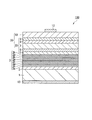
- FIG. 1 is a schematic cross-sectional view of a light-emitting diode according to the first embodiment.
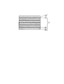
- FIG. 2 is a schematic sectional view of a laminated structure of a well layer and a barrier layer.
- the light emitting diode 100 according to the first embodiment is a light emitting diode including a DBR reflection layer 3 and a light emitting unit 20 in order on a substrate 1, and the light emitting unit 20 has a composition formula (Al X1 Ga 1-X1).
- An active layer 7 having a quantum well structure in which well layers 15 and barrier layers 16 made of a compound semiconductor of As (0 ⁇ X1 ⁇ 1) are alternately stacked, and a composition formula (Al X2 Ga 1 ⁇ X2 ) Y1 In 1-Y1 P (0 ⁇ X2 ⁇ 1, 0 ⁇ Y1 ⁇ 1), the first clad layer 5 and the second clad layer 6 made of a compound semiconductor.
- the number of pairs is 5 or less.
- the compound semiconductor layer (also referred to as an epitaxial growth layer) 30 has a structure in which a pn junction light emitting unit 20 and a current diffusion layer 10 are sequentially stacked.
- a known functional layer can be added to the structure of the compound semiconductor layer 30 as appropriate.
- the compound semiconductor layer 30 is preferably formed by epitaxial growth on a GaAs substrate.
- the light emitting unit 20 provided on the n-type substrate has an n-type lower cladding layer (first cladding layer) 5, a lower guide layer 6, an active layer 7 on the DBR reflection layer 3.
- An upper guide layer 8 and a p-type upper clad layer (second clad layer) 9 are sequentially laminated. That is, the light emitting unit 20 includes a lower clad layer 5 disposed opposite to the upper side and the upper side of the active layer 7 in order to “confine” the carrier (carrier) that causes radiative recombination and light emission in the active layer 7.
- a so-called double hetero (English abbreviation: DH) structure including the lower guide layer 6, the upper guide layer 8, and the upper cladding layer 9 is preferable in order to obtain high-intensity light emission.
- the active layer 7 forms a quantum well structure in order to control the emission wavelength of the light emitting diode (LED). That is, the active layer 7 has a multilayer structure (laminated structure) of the well layer 15 and the barrier layer 16 having a barrier layer (also referred to as a barrier layer) 16 at both ends.
- a barrier layer also referred to as a barrier layer
- the layer thickness of the active layer 7 is preferably in the range of 0.02 to 2 ⁇ m.
- the conductivity type of the active layer 7 is not particularly limited, and any of undoped, p-type and n-type can be selected. In order to increase the light emission efficiency, it is desirable that the crystallinity be undoped or the carrier concentration be less than 3 ⁇ 10 17 cm ⁇ 3 .
- DBR (Distributed Bragg Reflector) reflective layer 3 has two kinds of refractive indexes with a film thickness of ⁇ / (4n) ( ⁇ : wavelength of light to be reflected in vacuum, n: refractive index of layer material). It consists of a multilayer film in which layers are alternately stacked. When the difference between the two types of refractive indexes is large, a high reflectance can be obtained with a multilayer film having a relatively small number of layers. Instead of being reflected on a certain surface as in a normal reflecting film, the entire multilayer film is characterized by reflection based on the light interference phenomenon.
- the DBR (Distributed Bragg Reflector) reflecting layer 3 is preferably formed by alternately stacking 10 to 50 pairs of two types of layers having different refractive indexes. This is because when the number is 10 pairs or less, the reflectance is too low, so that it does not contribute to an increase in output, and even when the number is 50 pairs or more, the increase in reflectance is small.
- Two types of layers having different refractive indexes constituting the DBR (Distributed Bragg Reflector) reflecting layer 3 are two types of (Al Xh Ga 1-Xh ) Y3 In 1-Y3 P (0 ⁇ Xh ⁇ 1, Y3) having different compositions.
- a combination of AlGaInP having different compositions is preferable because it does not contain As that easily causes crystal defects, and GaInP and AlInP have the largest refractive index difference among them, so that the number of reflective layers can be reduced and the composition can be switched. Is also preferable because it is simple. Moreover, AlGaAs has an advantage that a large difference in refractive index is easily obtained.
- the well layer 15 is made of a compound semiconductor having a composition formula (Al X1 Ga 1-X1 ) As (0 ⁇ X1 ⁇ 1).
- the Al composition X1 is preferably 0 ⁇ X1 ⁇ 0.36.
- Table 1 shows the relationship between the Al composition X1 and the emission wavelength when the thickness of the well layer 15 is 7 nm. It can be seen that the lower the Al composition X1, the longer the emission wavelength. Moreover, from the tendency of the change, the Al composition corresponding to the emission wavelength not listed in the table can be estimated.
- the thickness of the well layer 15 is preferably in the range of 3 to 30 nm. More preferably, it is in the range of 3 to 10 nm.
- Table 4 shows the relationship between the thickness of the well layer 15 and the emission wavelength when the Al composition X1 of the well layer 15 is 0.02.
- the layer thickness decreases, the wavelength decreases due to the quantum effect.
- the emission wavelength is determined by the composition. Further, from the tendency of the change, the layer thickness corresponding to the emission wavelength not listed in the table can be estimated.
- the Al composition X1 and the layer thickness of the well layer 15 are obtained so that a desired emission wavelength within the range of 660 nm to 850 nm is obtained. Can be decided. For example, by setting the Al composition X1 of the well layer 15 to 0.20 ⁇ X1 ⁇ 0.36 and the thickness of the well layer 15 to 3 to 30 nm, a light emitting diode having an emission wavelength of 660 to 720 nm can be manufactured. it can.
- a light emitting diode having an emission wavelength of 720 to 850 nm can be manufactured.
- the barrier layer 16 is made of a compound semiconductor having a composition formula (Al X Ga 1-X ) As (0 ⁇ X ⁇ 1).
- X preferably has a composition with a larger band gap than the well layer 15 in order to prevent absorption in the barrier layer 16 and increase luminous efficiency.
- Al concentration is low from a crystalline viewpoint. Therefore, X is more preferably in the range of 0.1 to 0.4.
- the optimum X composition is determined by the relationship with the well layer composition. When the crystallinity is improved to reduce defects, light absorption is suppressed, and as a result, light emission output can be improved.
- the layer thickness of the barrier layer 16 is preferably equal to the layer thickness of the well layer 15 or thicker than the layer thickness of the well layer 15.
- the number of pairs in which the well layers 15 and barrier layers 16 having the quantum well structure forming the active layer 7 are alternately stacked is 5 or less, and one pair may be used.
- the carrier confinement effect is increased, the luminescence recombination probability of electrons and holes is increased, and a high response speed (rise time) of 25 nsec or less is secured.
- the response speed increased as the number of pairs of the well layer 15 and the barrier layer 16 was decreased from 5 to 1.
- the highest speed of 17 nsec was realized when the number of pairs was one.
- the junction capacitance (capacitance) of the PN junction increases. This is because the well layer 15 and the barrier layer 16 are undoped or have a low carrier concentration, so that the well layer 15 and the barrier layer 16 function as a depletion layer in the pn junction, and the thinner the depletion layer, the larger the capacitance. In general, it is desirable that the capacitance is small in order to increase the response speed. However, in the structure of the present invention, by reducing the number of the well layers 15 and the barrier layers 16, the response speed is increased even though the capacitance is increased. The effect is found. This is presumably because the effect of increasing the recombination rate of injected carriers by reducing the number of well layers 15 and barrier layers 16 is greater.
- junction area between the active layer 7 and the lower cladding layer 5 or the upper cladding layer 9 is preferably 20000 to 90000 ⁇ m 2 .
- the bonding area between the active layer 7 and the lower cladding layer 5 or the upper cladding layer 9 is 123000 ⁇ m 2 (350 ⁇ m ⁇ 350 ⁇ m) and narrower than that 53000 ⁇ m 2 (230 ⁇ m ⁇ 230 ⁇ m).
- the response speed is improved by about 10%, and when the number of pairs is 1, the response is 20%. Increased speed.
- the bonding area between the active layer 7 and the lower cladding layer 5 or the upper cladding layer 9 is 20000 ⁇ m 2 or more, the light output is not greatly reduced, and high output is secured.
- the number of pairs of the well layers 15 and the barrier layers 16 is 5 pairs.
- the light emission output was 6.4 mW (response speed 20 nsec), and even with one pair, a high light emission output of 5.8 mW (response speed 13 nsec) could be maintained.
- the lower guide layer 6 and the upper guide layer 8 are provided on the lower surface and the upper surface of the active layer 7, respectively. Specifically, the lower guide layer 6 is provided on the lower surface of the active layer 7, and the upper guide layer 8 is provided on the upper surface of the active layer 7.
- the lower guide layer 6 and the upper guide layer 8 have a composition of (Al X Ga 1-X ) As (0 ⁇ X ⁇ 1).
- the Al composition X is preferably a composition having a band gap equal to or larger than that of the barrier layer 15, and more preferably in the range of 0.2 to 0.6.
- the optimum X composition from the viewpoint of crystallinity is determined by the relationship with the composition of the well layer. When the crystallinity is improved to reduce defects, light absorption is suppressed, and as a result, light emission output can be improved.
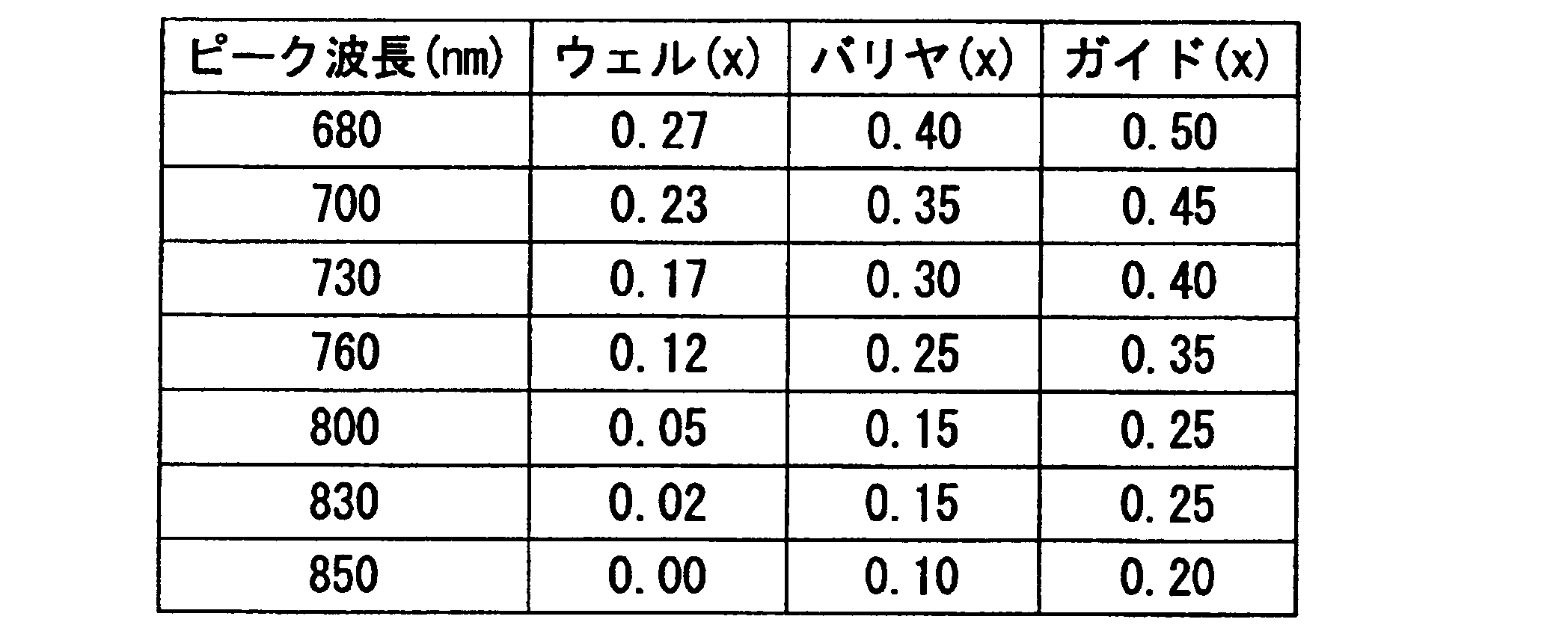
- Table 5 shows the Al composition X of the barrier layer 16 and the guide layer that maximizes the light emission output at the light emission wavelength when the well layer 15 has a layer thickness of 7 nm.
- the barrier layer and the guide layer preferably have a composition with a larger band gap than that of the well layer.
- the optimum composition is determined in relation to the composition of the well layer in order to improve the crystallinity and improve the light emission output. When the crystallinity is improved to reduce defects, light absorption is suppressed, and as a result, light emission output can be improved.
- the lower guide layer 6 and the upper guide layer 8 are provided in order to reduce the propagation of defects in the lower cladding layer 5, the upper cladding layer 9, and the active layer 7, respectively. That is, the V group constituent element of the lower guide layer 6, the upper guide layer 8 and the active layer 7 is arsenic (As), whereas in the present invention, the V group constituent element of the lower cladding layer 5 and the upper cladding layer 9 is phosphorus ( Therefore, defects are likely to occur at the interface. Propagation of defects to the active layer 7 causes a reduction in the performance of the light emitting diode. Therefore, the thickness of the lower guide layer 6 and the upper guide layer 8 is preferably 10 nm or more, and more preferably 20 nm to 100 nm.
- the conductivity types of the lower guide layer 6 and the upper guide layer 8 are not particularly limited, and any of undoped, p-type, and n-type can be selected. In order to increase the light emission efficiency, it is desirable that the crystallinity be undoped or the carrier concentration be less than 3 ⁇ 10 17 cm ⁇ 3 .
- the lower clad layer 5 and the upper clad layer 9 are provided on the lower surface of the lower guide layer 6 and the upper surface of the upper guide layer 8, respectively, as shown in FIG.
- the lower cladding layer 5 and the upper cladding layer 9 are made of a compound semiconductor of (Al X2 Ga 1-X2 ) Y1 In 1-Y1 P (0 ⁇ X2 ⁇ 1, 0 ⁇ Y1 ⁇ 1), and have a band higher than that of the barrier layer 16.
- a material having a large gap is preferable, and a material having a larger band gap than the lower guide layer 6 and the upper guide layer 8 is more preferable.
- the Al composition X2 of (Al X2 Ga 1-X2 ) Y1 In 1-Y1 P (0 ⁇ X2 ⁇ 1, 0 ⁇ Y1 ⁇ 1) has a composition of 0.3 to 0.7. It is preferable.
- Y1 is preferably 0.4 to 0.6.
- the lower cladding layer 5 and the upper cladding layer 9 are configured to have different polarities.
- the carrier concentration and thickness of the lower clad layer 5 and the upper clad layer 9 can be in a known suitable range, and it is preferable to optimize the conditions so that the luminous efficiency of the active layer 7 is increased. Further, the warpage of the compound semiconductor layer 2 can be reduced by controlling the composition of the lower cladding layer 5 and the upper cladding layer 9.
- the lower clad layer 5 for example, Mg-doped p-type (Al X2 Ga 1-X2 ) Y1 In 1-Y1 P (0.3 ⁇ X2 ⁇ 0.7, 0.4 ⁇ It is desirable to use a semiconductor material composed of Y1 ⁇ 0.6).
- the carrier concentration is preferably in the range of 2 ⁇ 10 17 to 2 ⁇ 10 18 cm ⁇ 3
- the layer thickness is preferably in the range of 0.1 to 1 ⁇ m.
- the upper clad layer 9 for example, Si-doped n-type (Al X2 Ga 1-X2 ) Y1 In 1-Y1 P (0.3 ⁇ X2 ⁇ 0.7, 0.4 ⁇ Y1 ⁇ 0) .6) is preferably used.
- the carrier concentration is preferably in the range of 1 ⁇ 10 17 to 1 ⁇ 10 18 cm ⁇ 3
- the layer thickness is preferably in the range of 0.1 to 1 ⁇ m.
- the polarities of the lower clad layer 5 and the upper clad layer 9 can be selected in consideration of the element structure of the compound semiconductor layer 2.
- a contact layer for lowering the contact resistance of the ohmic electrode a current diffusion layer for planarly diffusing the element driving current throughout the light emitting unit, and conversely
- a known layer structure such as a current blocking layer or a current confinement layer for limiting the region through which the element driving current flows can be provided.
- the current spreading layer 10 is provided below the light emitting unit 7.
- the current diffusion layer 10 relaxes strain generated by the active layer 12 when the compound semiconductor layer 2 is epitaxially grown on the GaAs substrate.
- the current spreading layer 10 may be made of a material that is transparent with respect to the emission wavelength from the light emitting unit 7 (active layer 7), for example, GaP.
- GaP When GaP is applied to the current diffusion layer 10, bonding can be facilitated and high bonding strength can be obtained by using the functional substrate 3 as a GaP substrate.
- the thickness of the current spreading layer 10 is preferably in the range of 0.5 to 20 ⁇ m. If the thickness is 0.5 ⁇ m or less, current diffusion is insufficient, and if it is 20 ⁇ m or more, the cost for crystal growth to the thickness increases.
- the p-type ohmic electrode (first electrode) 12 is a low-resistance ohmic contact electrode provided on the main light extraction surface of the light-emitting diode 100
- the n-type ohmic electrode (second electrode) 13 is a substrate of the light-emitting diode 100. It is a low-resistance ohmic contact electrode provided on the side back surface.
- the p-type ohmic electrode 12 is provided on the surface of the current diffusion layer 10, and for example, an alloy made of AuBe / Au or AuZn / Au can be used.
- the n-type ohmic electrode 13 can be made of, for example, an alloy made of AuGe or Ni alloy / Au.
- the compound semiconductor layer 30 shown in FIG. 1 includes an n-type GaAs substrate 1 on which a buffer layer 2 made of GaAs, a layer 3a made of GaInP (a layer having a high refractive index) 3a and a layer 3b made of AlInP (a layer having a low refractive index) 3b are alternately arranged.
- a current diffusion layer 10 made of type GaP is sequentially stacked.
- the GaAs substrate 1 a commercially available single crystal substrate manufactured by a known manufacturing method can be used.
- the surface on which the GaAs substrate 1 is epitaxially grown is preferably smooth.
- the plane orientation of the surface of the GaAs substrate 1 is easy to epitaxially grow, and a substrate that is turned off within ⁇ 20 ° from the (100) plane and (100) that are mass-produced is desirable from the standpoint of quality stability.
- the range of the plane orientation of the GaAs substrate 1 is more preferably 15 ° off ⁇ 5 ° from the (100) direction to the (0-1-1) direction.
- “-” means a bar attached to the index immediately after that.
- the dislocation density of the GaAs substrate 1 is desirably low in order to improve the crystallinity of the compound semiconductor layer 30. Specifically, for example, 10,000 pieces cm ⁇ 2 or less, preferably 1,000 pieces cm ⁇ 2 or less are suitable.
- the GaAs substrate 1 may be n-type or p-type.
- the carrier concentration of the GaAs substrate 1 can be appropriately selected from desired electrical conductivity and element structure.
- the carrier concentration is preferably in the range of 1 ⁇ 10 17 to 5 ⁇ 10 18 cm ⁇ 3 .
- the carrier concentration is preferably in the range of 2 ⁇ 10 18 to 5 ⁇ 10 19 cm ⁇ 3 .
- the thickness of the GaAs substrate 1 has an appropriate range depending on the size of the substrate. If the thickness of the GaAs substrate 1 is thinner than an appropriate range, the compound semiconductor layer 30 may be broken during the manufacturing process. On the other hand, if the thickness of the GaAs substrate 1 is thicker than an appropriate range, the material cost increases. For this reason, when the substrate size of the GaAs substrate 1 is large, for example, when the diameter is 75 mm, a thickness of 250 to 500 ⁇ m is desirable to prevent cracking during handling. Similarly, when the diameter is 50 mm, a thickness of 200 to 400 ⁇ m is desirable, and when the diameter is 100 mm, a thickness of 350 to 600 ⁇ m is desirable.
- the warpage of the compound semiconductor layer 30 caused by the light emitting portion 20 can be reduced.
- the temperature distribution during the epitaxial growth becomes uniform, so that the in-plane wavelength distribution of the active layer 7 can be reduced.
- the shape of the GaAs substrate 1 is not particularly limited to a circle, and there is no problem even if it is a rectangle or the like.
- the buffer layer (buffer) 2 is provided in order to reduce the propagation of defects between the GaAs substrate 1 and the constituent layers of the light emitting unit 20. For this reason, the buffer layer 2 is not necessarily required if the quality of the substrate and the epitaxial growth conditions are selected.
- the material of the buffer layer 2 is preferably the same as that of the substrate to be epitaxially grown. Therefore, in the present embodiment, it is preferable to use GaAs for the buffer layer 2 in the same manner as the GaAs substrate 1.
- the buffer layer 2 may be a multilayer film made of a material different from that of the GaAs substrate 1 in order to reduce the propagation of defects.
- the thickness of the buffer layer 2 is preferably 0.1 ⁇ m or more, and more preferably 0.2 ⁇ m or more.
- the DBR reflection layer 3 is provided to reflect light traveling in the substrate direction.
- the material of the DBR reflective layer 3 is preferably transparent with respect to the emission wavelength, and is preferably selected so as to be a combination that increases the difference in refractive index between the two types of materials constituting the DBR reflective layer 3.
- the material of the DBR reflection layer 3 is a combination of AlInP and GaInP, but two types of (Al Xl Ga 1-Xl ) 0.5 In 0.5 P (0 ⁇ xl ⁇ 1) having different compositions are used. , (Al Xh Ga 1-Xh ) 0.5 In 0.5 P (0 ⁇ xh ⁇ 1), and two types of Al xl Ga 1-xl As (0. It is also possible to select from 1 ⁇ xl ⁇ 1) and Al xh Ga 1-xh As (0.1 ⁇ xh ⁇ 1).
- a known growth method such as a molecular beam epitaxial method (MBE) or a low pressure metal organic chemical vapor deposition method (MOCVD method) can be applied.
- MBE molecular beam epitaxial method
- MOCVD method low pressure metal organic chemical vapor deposition method
- the MOCVD method which is excellent in mass productivity.
- the GaAs substrate 1 used for the epitaxial growth of the compound semiconductor layer 30 is preferably subjected to a pretreatment such as a cleaning process or a heat treatment before the growth to remove surface contamination or a natural oxide film.
- the layers constituting the compound semiconductor layer 30 can be laminated by setting a GaAs substrate 1 having a diameter of 50 to 150 mm in an MOCVD apparatus and simultaneously epitaxially growing the layers.
- the MOCVD apparatus a commercially available large-sized apparatus such as a self-revolving type or a high-speed rotating type can be applied.
- examples of the group III constituent material include trimethylaluminum ((CH 3 ) 3 Al), trimethylgallium ((CH 3 ) 3 Ga), and trimethylindium ((CH 3 ) 3 In) can be used.
- a Mg doping material for example, biscyclopentadienyl magnesium (bis- (C 5 H 5 ) 2 Mg) or the like can be used.
- a Si doping material for example, disilane (Si 2 H 6 ) or the like can be used.
- phosphine (PH 3 ), arsine (AsH 3 ), or the like can be used as a raw material for the group V constituent element.
- each layer As the growth temperature of each layer, 720 to 770 ° C. can be applied when p-type GaP is used as the current diffusion layer 10, and 600 to 700 ° C. can be applied to the other layers. Further, when p-type GaInP is used as the current diffusion layer 10, 600 to 700 ° C. can be applied. Furthermore, the carrier concentration, layer thickness, and temperature conditions of each layer can be selected as appropriate.
- the compound semiconductor layer 30 thus produced has a good surface state with few crystal defects despite having the light emitting portion 20.
- the compound semiconductor layer 30 may be subjected to surface processing such as polishing corresponding to the element structure.
- a p-type ohmic electrode 12 that is a first electrode and an n-type ohmic electrode 13 that is a second electrode are formed.
- the AlGaAs barrier layer 16 in the light emitting diode according to the first embodiment is composed of a composition formula (Al X3 Ga 1-X3 ) Y2 In 1-Y2 P (0 The difference is that the barrier layer is made of a compound semiconductor of ⁇ X3 ⁇ 1, 0 ⁇ Y2 ⁇ 1).
- the barrier layer is made of a compound semiconductor having a composition formula ( AlX3Ga1 -X3 ) Y2In1 -Y2P (0 ⁇ X3 ⁇ 1, 0 ⁇ Y2 ⁇ 1).
- the Al composition X3 is preferably a composition having a band gap larger than that of the well layer, and specifically in the range of 0 to 0.2.
- Y2 is preferably 0.4 to 0.6, and more preferably in the range of 0.45 to 0.55 in order to prevent generation of distortion due to lattice mismatch with the substrate.
- the layer thickness of the barrier layer is preferably equal to or greater than the layer thickness of the well layer.
- the layer thickness range in which the tunnel effect occurs By sufficiently thickening the layer thickness range in which the tunnel effect occurs, spreading between the well layers due to the tunnel effect is suppressed, the carrier confinement effect is increased, the probability of recombination of electrons and holes is increased, and the light emission output Can be improved.
- the light emitting diode manufactured in this example includes a light emitting diode having an active layer having a quantum well structure of a well layer made of AlGaAs and a barrier layer made of AlGaAs, and a barrier layer made of AlGaAs and a barrier layer made of AlGainP. And an infrared light emitting diode having an active layer having a quantum well structure.
- a light-emitting diode lamp in which a light-emitting diode chip was mounted on a substrate was prepared for characteristic evaluation.
- Example 1 The light-emitting diode of Example 1 was an example of the first embodiment, and the junction area between the active layer and the cladding layer was 123000 ⁇ m 2 (350 ⁇ m ⁇ 350 ⁇ m).
- an epitaxial wafer was fabricated by sequentially laminating compound semiconductor layers on a GaAs substrate made of an n-type GaAs single crystal doped with Si.
- the plane inclined by 15 ° from the (100) plane in the (0-1-1) direction was used as the growth plane, and the carrier concentration was set to 2 ⁇ 10 18 cm ⁇ 3 .
- the layer thickness of the GaAs substrate was about 0.5 ⁇ m.
- an n-type buffer layer made of GaAs doped with Si As the compound semiconductor layer, an n-type buffer layer made of GaAs doped with Si, an n-type DBR reflective layer having a 40-pair repeating structure of Si-doped AlInP and GaInP, and Si-doped (Al 0.7 N-type lower cladding layer made of Ga 0.3 ) 0.5 In 0.5 P, lower guide layer made of Al 0.4 Ga 0.6 As, Al 0.17 Ga 0.83 As / Al 0.
- Well layer / barrier layer composed of 3 Ga 0.7 As pairs
- upper guide layer composed of Al 0.4 Ga 0.6 As
- Mg-doped (Al 0.7 Ga 0.3 ) 0.5 In 0 .5 P p-type upper clad layer Mg-doped (Al 0.5 Ga 0.5 ) 0.5 In 0.5 P thin film intermediate layer
- Mg-doped p-type GaP current diffusion layer It was.
- a compound semiconductor layer was epitaxially grown on a GaAs substrate having a diameter of 76 mm and a thickness of 350 ⁇ m by using a low pressure metal organic chemical vapor deposition apparatus method (MOCVD apparatus) to form an epitaxial wafer.
- MOCVD apparatus metal organic chemical vapor deposition apparatus method
- trimethylaluminum ((CH 3 ) 3 Al), trimethylgallium ((CH 3 ) 3 Ga) and trimethylindium ((CH 3 ) 3 In) are used as the raw materials for the group III constituent elements did.
- biscyclopentadienyl magnesium bis- (C 5 H 5 ) 2 Mg
- disilane Si 2 H 6
- phosphine PH 3
- arsine As the growth temperature of each layer, the current diffusion layer made of p-type GaP was grown at 750 ° C. The other layers were grown at 700 ° C.
- the buffer layer made of GaAs has a carrier concentration of about 2 ⁇ 10 18 cm ⁇ 3 and a layer thickness of about 0.5 ⁇ m.
- the lower cladding layer had a carrier concentration of about 1 ⁇ 10 18 cm ⁇ 3 and a layer thickness of about 0.5 ⁇ m.
- the lower guide layer was undoped and had a thickness of about 50 nm.
- the well layer was undoped Al 0.17 Ga 0.83 As with a thickness of about 7 nm, and the barrier layer was undoped Al 0.3 Ga 0.7 As with a thickness of about 19 nm. Three pairs of well layers and barrier layers were alternately laminated.
- the upper guide layer was undoped and had a thickness of about 50 nm.
- the upper cladding layer had a carrier concentration of about 8 ⁇ 10 17 cm ⁇ 3 and a layer thickness of about 0.5 ⁇ m.
- the intermediate layer had a carrier concentration of about 8 ⁇ 10 17 cm ⁇ 3 and a layer thickness of about 50 nm.
- the current diffusion layer made of GaP has a carrier concentration of about 3 ⁇ 10 18 cm ⁇ 3 and a layer thickness of about 10 ⁇ m.
- DBR reflection layer and the carrier concentration of about 1 ⁇ 10 18 cm -3, and AlInP that were about 71nm thickness, carrier concentration of about 1 ⁇ 10 18 cm -3, a thickness of about 67nm was GaInP the 40 pairs were stacked.
- a film was formed on the surface of the current diffusion layer by vacuum vapor deposition so that AuBe was 0.2 ⁇ m and Au was 1 ⁇ m. Thereafter, patterning was performed using a general photolithography means, and a p-type ohmic electrode was formed as the first electrode. Next, a roughening treatment was performed on the light extraction surface which is a surface other than the electrode portion.
- a second electrode is formed on the back surface of the substrate by vacuum deposition so that AuGe and Ni alloy have a thickness of 0.5 ⁇ m, Pt of 0.2 ⁇ m, and Au of 1 ⁇ m, and an n-type ohmic electrode is formed. Formed. Thereafter, heat treatment was performed at 450 ° C. for 10 minutes to form an alloy, and low resistance p-type and n-type ohmic electrodes were formed.
- chips were cut from the compound semiconductor layer side at 350 ⁇ m intervals using a dicing saw.
- the crushing layer and dirt by dicing were removed by etching with a mixed solution of sulfuric acid and hydrogen peroxide to produce a light emitting diode of Example 1.
- This light-emitting diode lamp was manufactured by supporting (mounting) a mount with a die bonder, wire-bonding a p-type ohmic electrode and a p-electrode terminal with a gold wire, and sealing with a general epoxy resin.
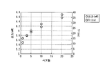
- FIG. 3 is a graph showing the relationship between the number of pairs of light emitting diodes and the output and response speed when the junction area between the active layer and the clad layer is 123000 ⁇ m 2
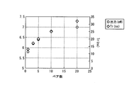
- FIG. 4 shows the junction between the active layer and the clad layer. It is a graph which shows the relationship between the number of pairs of a light emitting diode in case an area is 53000 micrometers 2 , output, and a response speed.
- Example 2 The light-emitting diode of Example 2 is an example of the first embodiment, and was manufactured under the same conditions as in Example 1 except that the number of pairs of well layers and barrier layers was three, and the same evaluation was performed. .
- the response speed (tr), the light emission output (P 0 ), and the forward voltage (V F ) were 18 nsec, 5.8 mW, and 1.6 V, respectively.
- Example 3 The light-emitting diode of Example 3 is an example of the first embodiment, and was manufactured under the same conditions as in Example 1 except that the number of pairs of well layers and barrier layers was five, and the same evaluation was performed. .
- the response speed (tr), the light emission output (P 0 ), and the forward voltage (V F ) were 21 nsec, 6.0 mW, and 1.6 V, respectively.
- Example 4 The light emitting diode of Example 4 was produced under the same conditions as in Example 3 except that the configuration of the DBR reflective layer was changed, and the same evaluation was performed.
- the DBR reflective layer has (Al 0.9 Ga 0.1 ) 0.5 In 0.5 P with a carrier concentration of about 1 ⁇ 10 18 cm ⁇ 3 and a layer thickness of about 71 nm, and a carrier concentration.
- (Al 0.2 Ga 0.8 ) 0.5 In 0.5 P were alternately stacked in a pair of about 1 ⁇ 10 18 cm ⁇ 3 and a layer thickness of about 68 nm.
- the response speed (tr), light emission output (P 0 ), and forward voltage (V F ) were 21 nsec, 5.7 mW, and 1.6 V, respectively.
- Example 5 The light emitting diode of Example 5 was produced under the same conditions as in Example 3 except that the configuration of the DBR reflective layer was changed, and the same evaluation was performed. Specifically, DBR reflective layer was about 1 ⁇ 10 18 carrier concentration cm -3, and Al 0.9 Ga 0.1 As that were about 71nm thickness, a carrier concentration of about 1 ⁇ 10 18 cm -3 40 pairs of Al 0.1 Ga 0.9 As having a layer thickness of about 64 nm were alternately laminated. The response speed (tr), the light emission output (P 0 ), and the forward voltage (V F ) were 20 nsec, 6.1 mW, and 1.6 V, respectively.
- the light emitting diodes of Examples 6 to 8 are also examples of the first embodiment, but are examples in which the junction area between the active layer and the clad layer is 53000 ⁇ m 2 (230 ⁇ m ⁇ 230 ⁇ m).
- Example 6 The light-emitting diode of Example 6 was fabricated under the same conditions as in Example 1 except for the junction area between the active layer and the cladding layer, and the same evaluation was performed.
- the response speed (tr), light emission output (P 0 ), and forward voltage (V F ) were 13 nsec, 5.8 mW, and 1.7 V, respectively.
- Example 7 The light emitting diode of Example 7 was fabricated under the same conditions as in Example 6 except that the number of pairs of the well layer and the barrier layer was 3, and the same evaluation was performed.
- the response speed (tr), light emission output (P 0 ), and forward voltage (V F ) were 17 nsec, 6.2 mW, and 1.7 V, respectively.
- Example 8 The light emitting diode of Example 8 was produced under the same conditions as in Example 6 except that the number of pairs of well layers and barrier layers was 5, and the same evaluation was performed.
- the response speed (tr), light emission output (P 0 ), and forward voltage (V F ) were 20 nsec, 6.4 mW, and 1.7 V, respectively.
- Example 9 Although the light emitting diode of Example 9 is also an example of the first embodiment, the junction area between the active layer and the cladding layer is 20000 ⁇ m 2 (200 ⁇ m ⁇ 100 ⁇ m).
- the light emitting diode of Example 9 was fabricated under the same conditions as in Example 3 except for the junction area between the active layer and the cladding layer, and the same evaluation was performed.
- the response speed (tr), light emission output (P 0 ), and forward voltage (V F ) were 17 nsec, 6.5 mW, and 1.8 V, respectively.
- Example 10 The light-emitting diode of Example 10 is also an example of the first embodiment, but is an example in which the junction area between the active layer and the cladding layer is 90000 ⁇ m 2 (300 ⁇ m ⁇ 300 ⁇ m).
- the light emitting diode of Example 10 was fabricated under the same conditions as in Example 3 except for the junction area between the active layer and the cladding layer, and the same evaluation was performed.
- the response speed (tr), light emission output (P 0 ), and forward voltage (V F ) were 21 nsec, 6.2 mW, and 1.6 V, respectively.
- the light emitting diodes of Examples 11 and 12 are examples of the second embodiment.
- the light-emitting diode of Example 11 is an example in which the junction area between the active layer and the cladding layer is 123000 ⁇ m 2 (350 ⁇ m ⁇ 350 ⁇ m).
- the layer structure of the light-emitting diode of Example 11 is as follows. First, an epitaxial wafer was fabricated by sequentially laminating compound semiconductor layers on a GaAs substrate made of an n-type GaAs single crystal doped with Si. In the GaAs substrate, the plane inclined by 15 ° from the (100) plane in the (0-1-1) direction was used as the growth plane, and the carrier concentration was set to 2 ⁇ 10 18 cm ⁇ 3 . The layer thickness of the GaAs substrate was about 0.5 ⁇ m.
- an n-type buffer layer made of GaAs doped with Si As the compound semiconductor layer, an n-type buffer layer made of GaAs doped with Si, an n-type DBR reflective layer having a 40-pair repeating structure of Si-doped AlInP and GaInP, and Si-doped (Al 0.7 N-type lower cladding layer made of Ga 0.3 ) 0.5 In 0.5 P, lower guide layer made of Al 0.4 Ga 0.6 As, Al 0.17 Ga 0.83 As / (Al 0 .1 Ga 0.9 ) 0.5 In 0.5 P well layer / barrier layer, Al 0.4 Ga 0.6 As upper guide layer, Mg doped (Al 0.7 Ga 0.3) p-type upper cladding layer composed of 0.5 in 0.5 P, an intermediate layer of a thin film made of (Al 0.5 Ga 0.5) 0.5 in 0.5 P, p which is Mg-doped A current spreading layer made of type GaP It was.
- the buffer layer made of GaAs has a carrier concentration of about 2 ⁇ 10 18 cm ⁇ 3 and a layer thickness of about 0.5 ⁇ m.
- the contact layer had a carrier concentration of about 2 ⁇ 10 18 cm ⁇ 3 and a layer thickness of about 3.5 ⁇ m.
- the upper cladding layer had a carrier concentration of about 1 ⁇ 10 18 cm ⁇ 3 and a layer thickness of about 0.5 ⁇ m.
- the upper guide layer was undoped and had a thickness of about 50 nm.
- the well layer is undoped Al 0.17 Ga 0.83 As with a layer thickness of about 7 nm, and the barrier layer is undoped (Al 0.1 Ga 0.9 ) 0.5 In 0. 5 P.
- the number of pairs of well layers and barrier layers was set to 5.
- the lower guide layer was undoped and had a thickness of about 50 nm.
- the lower cladding layer had a carrier concentration of about 8 ⁇ 10 17 cm ⁇ 3 and a layer thickness of about 0.5 ⁇ m.
- the intermediate layer had a carrier concentration of about 8 ⁇ 10 17 cm ⁇ 3 and a layer thickness of about 0.05 ⁇ m.
- the current diffusion layer made of GaP has a carrier concentration of about 3 ⁇ 10 18 cm ⁇ 3 and a layer thickness of about 9 ⁇ m.
- the response speed (tr), the light emission output (P 0 ), and the forward voltage (V F ) were 21 nsec, 5.8 mW, and 1.6 V, respectively.
- Example 12 The light-emitting diode of Example 12 was produced under the same conditions as Example 11 except that the junction area between the active layer and the cladding layer was 53000 ⁇ m 2 (230 ⁇ m ⁇ 230 ⁇ m), and the same evaluation was performed.
- the response speed (tr), light emission output (P 0 ), and forward voltage (V F ) were 20 nsec, 6.3 mW, and 1.7 V, respectively.
- Reference Examples 1 to 4 are examples in which the number of pairs of the well layer and the barrier layer is 10 pairs and 20 pairs.
- the ternary mixed crystal quantum well structure of the present invention or the ternary mixed crystal well layer and the quaternary mixed layer are used. This is to show that a structure in which a quantum well structure composed of a crystal barrier layer is sandwiched between quaternary cladding layers is suitable for high light emission output.
- Reference Example 1 The light emitting diode of Reference Example 1 was produced under the same conditions as the light emitting diode of Example 1 except that the number of pairs of well layers and barrier layers was 10, and the same evaluation was performed.
- the response speed (tr), light emission output (P 0 ), and forward voltage (V F ) were 26 nsec, 6.3 mW, and 1.6 V, respectively.
- Reference Example 2 The light emitting diode of Reference Example 2 was produced under the same conditions as those of the light emitting diode of Example 1 except that the number of pairs of well layers and barrier layers was 20, and the same evaluation was performed.
- the response speed (tr), light emission output (P 0 ), and forward voltage (V F ) were 35 nsec, 6.7 mW, and 1.6 V, respectively.
- Reference Example 3 The light emitting diode of Reference Example 3 was produced under the same conditions as the light emitting diode of Example 6 except that the number of pairs of well layers and barrier layers was 10, and the same evaluation was performed.
- the response speed (tr), the light emission output (P 0 ), and the forward voltage (V F ) were 25 nsec, 6.8 mW, and 1.7 V, respectively.
- Reference Example 4 The light emitting diode of Reference Example 4 was produced under the same conditions as those of the light emitting diode of Example 6 except that the number of pairs of well layers and barrier layers was 20, and the same evaluation was performed.
- the response speed (tr), light emission output (P 0 ), and forward voltage (V F ) were 32 nsec, 7.0 mW, and 1.7 V, respectively.
- Comparative Example 1 An example of a light emitting diode having a light emission wavelength of 760 nm having a structure in which a thick film is grown and a substrate is removed by a liquid phase epitaxial method is shown.
- An AlGaAs layer was grown on a GaAs substrate using a slide boat type growth apparatus.
- a p-type GaAs substrate was set in a substrate storage groove of a slide boat type growth apparatus, and Ga metal, GaAs polycrystal, metal Al, and a dopant were put in a crucible prepared for growth of each layer.
- the growing layer has a four-layer structure of a transparent thick film layer (first p-type layer), a lower clad layer (p-type clad layer), an active layer, and an upper clad layer (n-type clad layer).
- a slide boat type growth apparatus in which these raw materials are set is set in a quartz reaction tube, heated to 950 ° C. in a hydrogen stream, dissolved, and then the ambient temperature is lowered to 910 ° C. After pressing and bringing into contact with the raw material solution (melt), the temperature is lowered at a rate of 0.5 ° C./min. After reaching the predetermined temperature, the operation of repeatedly touching each raw material solution after pressing the slider is repeated repeatedly. Specifically, after contact with the melt, the atmospheric temperature was lowered to 703 ° C. to grow the n-clad layer, and then the slider was pushed to separate the raw material solution from the wafer to complete the epitaxial growth.
- the epitaxial substrate was taken out, the surface of the n-type GaAlAs cladding layer was protected, and the p-type GaAs substrate was selectively removed with an ammonia-hydrogen peroxide etchant. Thereafter, gold electrodes were formed on both sides of the epitaxial wafer, and a surface electrode in which a wire bonding pad having a diameter of 100 ⁇ m was arranged at the center was formed using an electrode mask having a long side of 350 ⁇ m. On the back electrode, ohmic electrodes having a diameter of 20 ⁇ m were formed at intervals of 80 ⁇ m. Thereafter, separation and etching were performed by dicing, so that a 350 ⁇ m square light-emitting diode in which the n-type GaAlAs layer was on the surface side was produced.
- Table 6 shows the results of mounting the light-emitting diode of Comparative Example 1 and evaluating the characteristics of the light-emitting diode lamp.
- Table 6 when current was passed between the n-type and p-type ohmic electrodes, infrared light having a peak wavelength of 760 nm was emitted.
- the forward voltage (V F ) when a current of 20 mA (mA) was passed in the forward direction was 1.9 volts (V).
- the response speed (tr) and the light emission output (P 0 ) when the forward current was 20 mA were 25 nsec and 3.0 mW, respectively.
- the response speed was equal or slower than that of Examples 1 to 16 of the present invention, and the light emission output was low.
- the light-emitting diode, light-emitting diode lamp, and lighting device of the present invention can be used as a light-emitting diode, a light-emitting diode lamp, and a lighting device that emit red light and / or infrared light having both high-speed response and high output.
Landscapes
- Led Devices (AREA)
Abstract
高速応答性と高出力性とを兼ね備えた赤色光及び/又は赤外光を発光する発光ダイオード、発光ダイオードランプ及び照明装置が提供される。そのような発光ダイオードは、基板上に、DBR反射層と、発光部とを順に備える発光ダイオードであって、発光部は、組成式(AlX1Ga1-X1)As(0≦X1≦1)の化合物半導体からなる井戸層及びバリア層を交互に積層した量子井戸構造の活性層と、該活性層を挟む、組成式(AlX2Ga1-X2)Y1In1-Y1P(0≦X2≦1,0<Y1≦1)の化合物半導体からなる第1のクラッド層及び第2のクラッド層とを有し、井戸層及びバリア層のペア数が5以下である。
Description
本発明は、発光ダイオード、発光ダイオードランプ及び照明装置に関するものであり、特に高速応答性と高出力性を備えた赤色光又は赤外光を発光する発光ダイオード、発光ダイオードランプ及び照明装置に関する。
本願は、2011年3月3日に、日本に出願された特願2011-046255号に基づき優先権を主張し、その内容をここに援用する。
本願は、2011年3月3日に、日本に出願された特願2011-046255号に基づき優先権を主張し、その内容をここに援用する。
赤色光又は赤外光を発光する発光ダイオードは、通信、各種センサー、夜間照明、植物工場用の光源など用途が広がっている。
それに応じて、赤色光又は赤外光を発光する発光ダイオードに対する要求は、主に高出力性を重視するもの、あるいは、主に高速応答性を重視するものから、それらの両方を重視するものへと変化している。特に、通信用の発光ダイオードでは、大容量の光空間伝送を行うため、高速応答性と高出力性とが必須である。
それに応じて、赤色光又は赤外光を発光する発光ダイオードに対する要求は、主に高出力性を重視するもの、あるいは、主に高速応答性を重視するものから、それらの両方を重視するものへと変化している。特に、通信用の発光ダイオードでは、大容量の光空間伝送を行うため、高速応答性と高出力性とが必須である。
赤色光及び赤外光を発光する発光ダイオードとして、GaAs基板にAlGaAs活性層を含む化合物半導体層を液相エピタキシャル法で成長させた発光ダイオードが知られている(例えば、特許文献1~4)。
特許文献4において、液相エピタキシャル法を用いてGaAs基板にAlGaAs活性層を含む化合物半導体層を成長させ、その後、成長基板として用いたGaAs基板を除去する、いわゆる基板除去型の発光ダイオードが開示されている。特許文献4において開示された発光ダイオードでは、応答速度(立ち上がり時間)が40~55nsec程度においては出力が4mW以下である。また、応答速度が20nsec程度においては出力が5mWを若干超えた程度であり、液相エピタキシャル法を用いて作製した発光ダイオードとしては現在最も高い応答速度で高出力のものであると思われる。
しかしながら、上記の出力では通信用の発光ダイオードとしては十分ではない。 発光ダイオードは半導体レーザーと異なり、自然放出光を利用しているため、高速応答性と高出力性とはトレードオフの関係にある。従って、例えば、単に発光層の層厚を薄くしてキャリアの閉じ込め効果を増大して電子と正孔の発光再結合確率を高め、高速応答化を図っても、発光出力は低下してしまうという問題がある。
本発明は、上記事情を鑑みてなされたものであり、高速応答性と高出力性とを兼ね備えた赤色光及び/又は赤外光を発光する発光ダイオード、発光ダイオードランプ及び照明装置を提供することを目的とする。
本発明者は、上記課題を解決するために鋭意研究を重ねた結果、AlGaAs井戸層とAlGaAs又は4元混晶のAlGaInPからなるバリア層とを交互に5ペア以下積層した量子井戸構造を活性層とし、この活性層を挟むクラッド層を4元混晶のAlGaInPからなるものとする構成とすることにより、高速応答性を維持しつつ、高出力で赤色光及び/又は赤外光を発光する発光ダイオードを完成させた。
この際、本発明者は、まず、高いキャリアの閉じ込め効果を有し、高速応答に適した量子井戸構造を活性層に採用すると共に、高い注入キャリア密度を確保するために井戸層及びバリア層のペア数を5以下とした。この構成により、液相エピタキシャル法を用いて作製された発光ダイオードの上記の最も高速の応答速度と同程度か若しくはそれ以上の応答速度を実現した。
また、3元混晶の量子井戸構造又3元混晶の井戸層と4元混晶のバリア層とからなる量子井戸構造を挟むクラッド層に、バンドギャップが大きくて発光波長に対して透明であり、かつ、欠陥を作りやすいAsを含まないので結晶性の良い4元混晶のAlGaInPを採用した。
この際、本発明者は、まず、高いキャリアの閉じ込め効果を有し、高速応答に適した量子井戸構造を活性層に採用すると共に、高い注入キャリア密度を確保するために井戸層及びバリア層のペア数を5以下とした。この構成により、液相エピタキシャル法を用いて作製された発光ダイオードの上記の最も高速の応答速度と同程度か若しくはそれ以上の応答速度を実現した。
また、3元混晶の量子井戸構造又3元混晶の井戸層と4元混晶のバリア層とからなる量子井戸構造を挟むクラッド層に、バンドギャップが大きくて発光波長に対して透明であり、かつ、欠陥を作りやすいAsを含まないので結晶性の良い4元混晶のAlGaInPを採用した。
以上の通り、本発明者は、5ペア以下の量子井戸構造を活性層とする構成を採用して高速応答性を確保し、この構成において、3元混晶の量子井戸構造又3元混晶の井戸層と4元混晶のバリア層とからなる量子井戸構造を挟むクラッド層に4元混晶を用いる構成という画期的な組み合わせを採用すると共に、化合物半導体層の成長に用いた成長基板を除去して光吸収のない基板に改めて化合物半導体層を貼り付けた構成を採用することにより、高出力化を図ることに成功したのである。
本発明は、以下の手段を提供する。
(1)基板上に、DBR反射層と、発光部とを順に備える発光ダイオードであって、前記発光部は、組成式(AlX1Ga1-X1)As(0≦X1≦1)の化合物半導体からなる井戸層及びバリア層を交互に積層した量子井戸構造の活性層と、該活性層を挟む、組成式(AlX2Ga1-X2)Y1In1-Y1P(0≦X2≦1,0<Y1≦1)の化合物半導体からなる第1のクラッド層及び第2のクラッド層とを有し、前記井戸層及びバリア層のペア数が5以下であることを特徴とする発光ダイオード。
(2)基板上に、DBR反射層と、発光部とを順に備える発光ダイオードであって、前記発光部は、組成式(AlX1Ga1-X1)As(0≦X1≦1)の化合物半導体からなる井戸層と、組成式(AlX3Ga1-X3)Y2In1-Y2P(0≦X3≦1,0<Y2≦1)の化合物半導体からなるバリア層を交互に積層した量子井戸構造の活性層と、該活性層を挟む、組成式(AlX2Ga1-X2)Y1In1-Y1P(0≦X2≦1,0<Y1≦1)の化合物半導体からなる第1のクラッド層及び第2のクラッド層とを有し、前記井戸層及びバリア層のペア数が5以下であることを特徴とする発光ダイオード。
(3)前記活性層と前記クラッド層との接合面積が20000~90000μm2であることを特徴とする前項(1)または(2)のいずれかに記載の発光ダイオード。
なお、「前記活性層と前記クラッド層との接合面積」とは、ガイド層等の層を介して活性層とクラッド層とが接合されている場合には、それらの層と活性層若しくはクラッド層との間の接合面積を意味する。
(4)前記井戸層のAl組成X1を0.20≦X1≦0.36とし、前記井戸層の厚さを3~30nmとし、発光波長が660~720nmに設定されてなることを特徴とする前項(1)から(3)のいずれか一項に発光ダイオード。
(5)前記井戸層のAl組成X1を0≦X1≦0.2とし、前記井戸層の厚さを3~30nmとし、発光波長が720~850nmに設定されてなることを特徴とする前項(1)から(3)のいずれか一項に発光ダイオード。
(6)前記DBR反射層は屈折率の異なる2種類の層が交互に10~50対積層されてなることを特徴とする前項(1)から(5)のいずれか一項に発光ダイオード。
(7)前記屈折率の異なる2種類の層は組成の異なる2種類の(AlXhGa1-Xh)Y3In1-Y3P(0<Xh≦1、Y3=0.5)、(AlXlGa1-Xl)Y3In1-Y3P;0≦Xl<1、Y3=0.5)の組み合わせであり、両者のAlの組成差ΔX=xh-xlが0.5より大きいか又は等しいことを特徴とする前項(6)に記載の発光ダイオード。
(8)前記屈折率の異なる2種類の層はGaInPとAlInPの組み合わせであることを特徴とする前項(6)に記載の発光ダイオード。
(9)前記屈折率の異なる2種類の層は組成の異なる2種類のAlxlGa1-xlAs(0.1≦xl≦1)、AlxhGa1-xhAs(0.1≦xh≦1)の組み合わせであり、両者のAlの組成差ΔX=xh-xlが0.5より大きいか又は等しいことを特徴とする前項(6)に記載の発光ダイオード。
(10)前記発光部の、DBR反射層の反対側の面上に電流拡散層を備えることを特徴とする前項(1)から(9)のいずれか一項に記載の発光ダイオード。
(1)基板上に、DBR反射層と、発光部とを順に備える発光ダイオードであって、前記発光部は、組成式(AlX1Ga1-X1)As(0≦X1≦1)の化合物半導体からなる井戸層及びバリア層を交互に積層した量子井戸構造の活性層と、該活性層を挟む、組成式(AlX2Ga1-X2)Y1In1-Y1P(0≦X2≦1,0<Y1≦1)の化合物半導体からなる第1のクラッド層及び第2のクラッド層とを有し、前記井戸層及びバリア層のペア数が5以下であることを特徴とする発光ダイオード。
(2)基板上に、DBR反射層と、発光部とを順に備える発光ダイオードであって、前記発光部は、組成式(AlX1Ga1-X1)As(0≦X1≦1)の化合物半導体からなる井戸層と、組成式(AlX3Ga1-X3)Y2In1-Y2P(0≦X3≦1,0<Y2≦1)の化合物半導体からなるバリア層を交互に積層した量子井戸構造の活性層と、該活性層を挟む、組成式(AlX2Ga1-X2)Y1In1-Y1P(0≦X2≦1,0<Y1≦1)の化合物半導体からなる第1のクラッド層及び第2のクラッド層とを有し、前記井戸層及びバリア層のペア数が5以下であることを特徴とする発光ダイオード。
(3)前記活性層と前記クラッド層との接合面積が20000~90000μm2であることを特徴とする前項(1)または(2)のいずれかに記載の発光ダイオード。
なお、「前記活性層と前記クラッド層との接合面積」とは、ガイド層等の層を介して活性層とクラッド層とが接合されている場合には、それらの層と活性層若しくはクラッド層との間の接合面積を意味する。
(4)前記井戸層のAl組成X1を0.20≦X1≦0.36とし、前記井戸層の厚さを3~30nmとし、発光波長が660~720nmに設定されてなることを特徴とする前項(1)から(3)のいずれか一項に発光ダイオード。
(5)前記井戸層のAl組成X1を0≦X1≦0.2とし、前記井戸層の厚さを3~30nmとし、発光波長が720~850nmに設定されてなることを特徴とする前項(1)から(3)のいずれか一項に発光ダイオード。
(6)前記DBR反射層は屈折率の異なる2種類の層が交互に10~50対積層されてなることを特徴とする前項(1)から(5)のいずれか一項に発光ダイオード。
(7)前記屈折率の異なる2種類の層は組成の異なる2種類の(AlXhGa1-Xh)Y3In1-Y3P(0<Xh≦1、Y3=0.5)、(AlXlGa1-Xl)Y3In1-Y3P;0≦Xl<1、Y3=0.5)の組み合わせであり、両者のAlの組成差ΔX=xh-xlが0.5より大きいか又は等しいことを特徴とする前項(6)に記載の発光ダイオード。
(8)前記屈折率の異なる2種類の層はGaInPとAlInPの組み合わせであることを特徴とする前項(6)に記載の発光ダイオード。
(9)前記屈折率の異なる2種類の層は組成の異なる2種類のAlxlGa1-xlAs(0.1≦xl≦1)、AlxhGa1-xhAs(0.1≦xh≦1)の組み合わせであり、両者のAlの組成差ΔX=xh-xlが0.5より大きいか又は等しいことを特徴とする前項(6)に記載の発光ダイオード。
(10)前記発光部の、DBR反射層の反対側の面上に電流拡散層を備えることを特徴とする前項(1)から(9)のいずれか一項に記載の発光ダイオード。
本発明の発光ダイオードによれば、AlGaAsからなる井戸層及びバリア層を交互に積層した量子井戸構造の活性層、又は、AlGaAsからなる井戸層とAlGaInPからなるバリア層とを交互に積層した量子井戸構造の活性層を採用し、注入キャリアの閉じ込め効果が大きい量子井戸を用いる構成としたので、井戸層内に十分な注入キャリアが閉じ込められることにより、井戸層内のキャリア密度が高くなり、その結果、発光再結合確率が増大して、応答速度が向上した。
また、量子井戸構造内に注入されたキャリアはその波動性のためにトンネル効果によって量子井戸構造内の井戸層間全体に広がることになるが、量子井戸構造の井戸層及びバリア層のペア数を5以下とする構成を採用したので、その広がりによる注入キャリアの閉じ込め効果の低下を極力回避し、高速応答性が担保されている。
さらにまた、量子井戸構造の活性層から発光する構成なので単色性が高い。
また、活性層を挟む第1のクラッド層及び第2のクラッド層として、発光波長に対して透明であると共に、欠陥を作りやすいAsを含まないために結晶性が高いAlGaInPからなる構成を採用したので、欠陥を介した電子と正孔の非発光再結合確率が低下し、発光出力が向上した。
さらに、活性層を挟む第1のクラッド層及び第2のクラッド層として、4元混晶のAlGaInPからなる構成を採用したので、クラッド層が3元混晶からなる発光ダイオードに比べてAl濃度が低く、耐湿性が向上した。
発光層と基板との間にDBR反射膜を備える構成なので、GaAs基板による光の吸収によって発光出力が低下するのを回避することができる。
また、量子井戸構造内に注入されたキャリアはその波動性のためにトンネル効果によって量子井戸構造内の井戸層間全体に広がることになるが、量子井戸構造の井戸層及びバリア層のペア数を5以下とする構成を採用したので、その広がりによる注入キャリアの閉じ込め効果の低下を極力回避し、高速応答性が担保されている。
さらにまた、量子井戸構造の活性層から発光する構成なので単色性が高い。
また、活性層を挟む第1のクラッド層及び第2のクラッド層として、発光波長に対して透明であると共に、欠陥を作りやすいAsを含まないために結晶性が高いAlGaInPからなる構成を採用したので、欠陥を介した電子と正孔の非発光再結合確率が低下し、発光出力が向上した。
さらに、活性層を挟む第1のクラッド層及び第2のクラッド層として、4元混晶のAlGaInPからなる構成を採用したので、クラッド層が3元混晶からなる発光ダイオードに比べてAl濃度が低く、耐湿性が向上した。
発光層と基板との間にDBR反射膜を備える構成なので、GaAs基板による光の吸収によって発光出力が低下するのを回避することができる。
本発明の発光ダイオードによれば、活性層とクラッド層との接合面積を20000~90000μm2である構成を採用することにより、その接合面積を90000μm2以下とすることで電流密度が高くなり、高出力を担保しつつ、発光再結合確率が増大して応答速度が向上する。他方、20000μm2以上とすることで、通電電流に対する発光出力の飽和を抑制することにより、発光出力の大きな低下がなく、高出力が担保される。
本発明の発光ダイオードによれば、井戸層のAl組成X1を0.20≦X1≦0.36とし、井戸層の厚さを3~30nmとし、発光波長が660~720nmに設定されてなる構成を採用することにより、従来の660~720nmの赤色発光ダイオードに比べて応答速度が高くかつ高出力が実現される。
本発明の発光ダイオードによれば、井戸層のAl組成X1を0≦X1≦0.2とし、井戸層の厚さを3~30nmとし、発光波長が720~850nmに設定されてなる構成を採用することにより、従来の720~850nmの赤外発光ダイオードに比べて応答速度が高くかつ高出力が実現される。
以下、本発明を適用した一実施形態である発光ダイオードについて図面を用いて詳細に説明する。なお、以下の説明で用いる図面において、同一部材には同一符号を付し若しくは符号を省略する。また、以下の説明で用いる図面は模式的であり、長さ、幅、及び厚みの比率等は現実のものとは異なる場合がある。
<発光ダイオード(第1の実施形態)>
図1は、第1の実施形態に係る発光ダイオードの断面模式図である。また、図2は井戸層とバリア層の積層構造の断面模式図である。
第1の実施形態に係る発光ダイオード100は、基板1上に、DBR反射層3と、発光部20とを順に備える発光ダイオードであって、発光部20は、組成式(AlX1Ga1-X1)As(0≦X1≦1)の化合物半導体からなる井戸層15及びバリア層16を交互に積層した量子井戸構造の活性層7と、該活性層7を挟む、組成式(AlX2Ga1-X2)Y1In1-Y1P(0≦X2≦1,0<Y1≦1)の化合物半導体からなる第1のクラッド層5及び第2のクラッド層6とを有し、井戸層及びバリア層のペア数が5以下であることを特徴とするものである。
図1は、第1の実施形態に係る発光ダイオードの断面模式図である。また、図2は井戸層とバリア層の積層構造の断面模式図である。
第1の実施形態に係る発光ダイオード100は、基板1上に、DBR反射層3と、発光部20とを順に備える発光ダイオードであって、発光部20は、組成式(AlX1Ga1-X1)As(0≦X1≦1)の化合物半導体からなる井戸層15及びバリア層16を交互に積層した量子井戸構造の活性層7と、該活性層7を挟む、組成式(AlX2Ga1-X2)Y1In1-Y1P(0≦X2≦1,0<Y1≦1)の化合物半導体からなる第1のクラッド層5及び第2のクラッド層6とを有し、井戸層及びバリア層のペア数が5以下であることを特徴とするものである。
化合物半導体層(エピタキシャル成長層ともいう)30は、図1に示すように、pn接合型の発光部20と電流拡散層10とが順次積層された構造を有している。この化合物半導体層30の構造には、公知の機能層を適時加えることができる。例えば、オーミック(Ohmic)電極の接触抵抗を下げるためのコンタクト層、素子駆動電流を発光部の全般に平面的に拡散させるための電流拡散層、逆に素子駆動電流の通流する領域を制限するための電流阻止層や電流狭窄層など公知の層構造を設けることができる。
なお、化合物半導体層30は、GaAs基板上にエピタキシャル成長させて形成されたものであることが好ましい。
なお、化合物半導体層30は、GaAs基板上にエピタキシャル成長させて形成されたものであることが好ましい。
n型基板上に備える発光部20は例えば、図1に示すように、DBR反射層3上に、n型の下部クラッド層(第1のクラッド層)5、下部ガイド層6、活性層7、上部ガイド層8、p型の上部クラッド層(第2のクラッド層)9が順次積層されて構成されている。すなわち、発光部20は、放射再結合をもたらすキャリア(担体;carrier)及び発光を活性層7に「閉じ込める」ために、活性層7の下側及び上側に対峙して配置した下部クラッド層5、下部ガイド(guide)層6、及び上部ガイド層8、上部クラッド層9を含む、所謂、ダブルヘテロ(英略称:DH)構造とすることが高強度の発光を得る上で好ましい。
活性層7は、図2に示すように、発光ダイオード(LED)の発光波長を制御するため、量子井戸構造を構成する。すなわち、活性層7は、バリア層(障壁層ともいう)16を両端に有する、井戸層15とバリア層16との多層構造(積層構造)である。
活性層7の層厚は、0.02~2μmの範囲であることが好ましい。また、活性層7の伝導型は特に限定されるものではなく、アンドープ、p型及びn型のいずれも選択することができる。発光効率を高めるには、結晶性が良好なアンドープ又は3×1017cm-3未満のキャリア濃度とすることが望ましい。
DBR(Distributed Bragg Reflector)反射層3は、λ/(4n)の膜厚で(λ:反射すべき光の真空中での波長、n:層材料の屈折率)、屈折率が異なる2種類の層を交互に積層した多層膜からなるものである。反射率は2種類の屈折率の差が大きいと、比較的少ない層数の多層膜で高反射率が得られる。通常の反射膜のようにある面で反射されるのでなく、多層膜の全体で光の干渉現象に基づき反射が起きることが特徴である。
DBR(Distributed Bragg Reflector)反射層3は、屈折率の異なる2種類の層が交互に10~50対積層されてなるのが好ましい。10対以下である場合は反射率が低すぎるために出力の増大に寄与せず、50対以上にしてもさらなる反射率の増大は小さいからである。
DBR(Distributed Bragg Reflector)反射層3を構成する屈折率の異なる2種類の層は、組成の異なる2種類の(AlXhGa1-Xh)Y3In1-Y3P(0<Xh≦1、Y3=0.5)、(AlXlGa1-Xl)Y3In1-Y3P;0≦Xl<1、Y3=0.5)の対であり、両者のAlの組成差ΔX=xh-xlが0.5より大きいか又は等しくなる組み合わせか、又は、GaInPとAlInPの組み合わせか、又は、組成の異なる2種類のAlxlGa1-xlAs(0.1≦xl≦1)、AlxhGa1-xhAs(0.1≦xh≦1)の対であり、両者の組成差ΔX=xh-xlが0.5より大きいか等しくなる組み合わせかのいずれかから選択されるのが効率よく高い反射率が得られることから望ましい。
組成の異なるAlGaInPの組み合わせは、結晶欠陥を生じやすいAsを含まないので好ましく、GaInPとAlInPはその中で屈折率差を最も大きくとれるので、反射層の数を少なくすることができ、組成の切り替えも単純であるので好ましい。また、AlGaAsは、大きな屈折率差をとりやすいという利点がある。
DBR(Distributed Bragg Reflector)反射層3を構成する屈折率の異なる2種類の層は、組成の異なる2種類の(AlXhGa1-Xh)Y3In1-Y3P(0<Xh≦1、Y3=0.5)、(AlXlGa1-Xl)Y3In1-Y3P;0≦Xl<1、Y3=0.5)の対であり、両者のAlの組成差ΔX=xh-xlが0.5より大きいか又は等しくなる組み合わせか、又は、GaInPとAlInPの組み合わせか、又は、組成の異なる2種類のAlxlGa1-xlAs(0.1≦xl≦1)、AlxhGa1-xhAs(0.1≦xh≦1)の対であり、両者の組成差ΔX=xh-xlが0.5より大きいか等しくなる組み合わせかのいずれかから選択されるのが効率よく高い反射率が得られることから望ましい。
組成の異なるAlGaInPの組み合わせは、結晶欠陥を生じやすいAsを含まないので好ましく、GaInPとAlInPはその中で屈折率差を最も大きくとれるので、反射層の数を少なくすることができ、組成の切り替えも単純であるので好ましい。また、AlGaAsは、大きな屈折率差をとりやすいという利点がある。
井戸層15は、組成式(AlX1Ga1-X1)As(0≦X1≦1)の化合物半導体からなる。
Al組成X1は0≦X1≦0.36であるのが好ましい。Al組成X1をこの範囲とすることにより、660nm~850nmの範囲で所望の発光波長を有するものとすることができる。
表1に、井戸層15の層厚が7nmのとき、Al組成X1と発光波長との関係を示す。
Al組成X1が低くなるほど、発光波長が長くなっていることがわかる。また、その変化の傾向から、表に掲載されていない発光波長に対応する、Al組成を推定することができる。
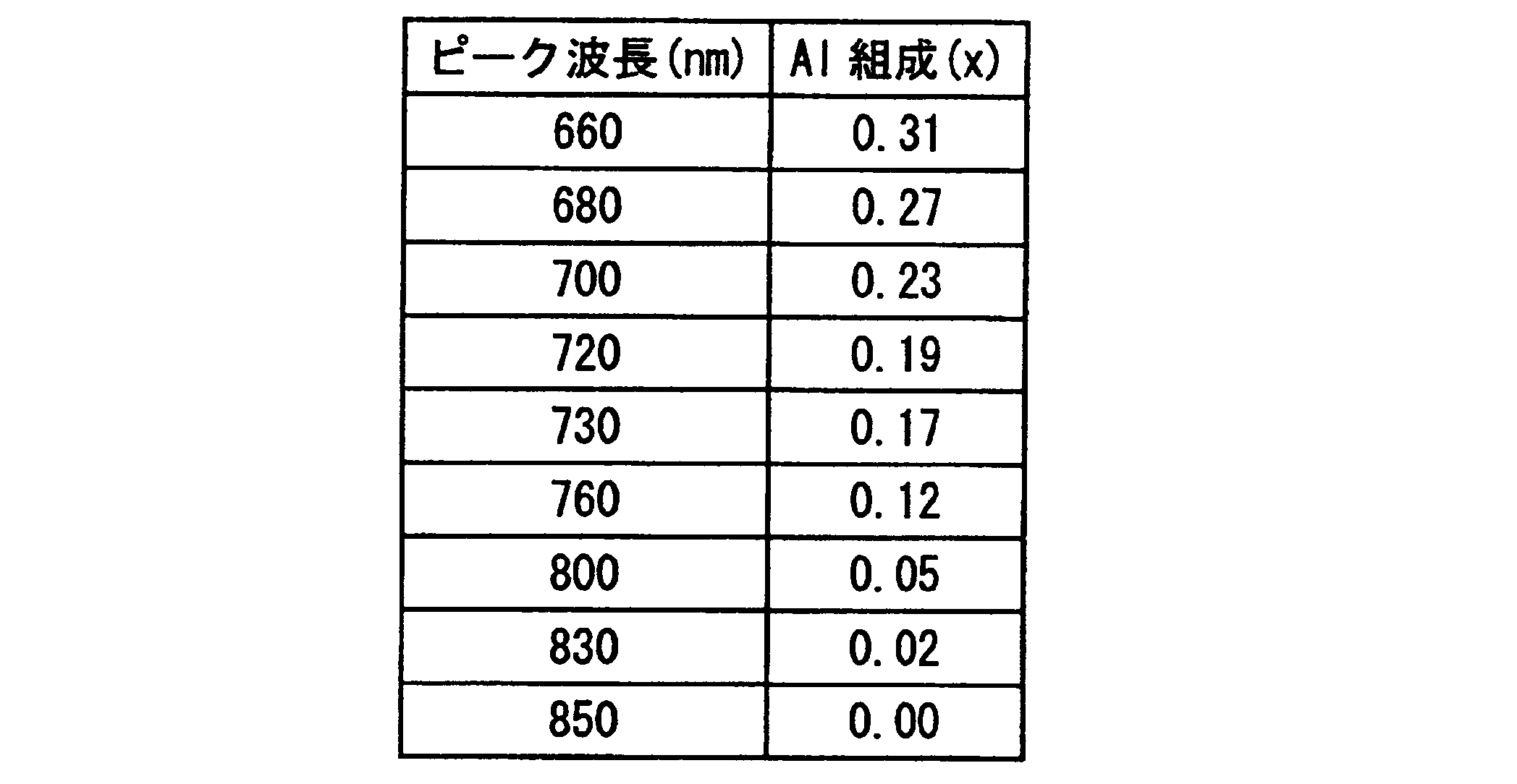
Al組成X1は0≦X1≦0.36であるのが好ましい。Al組成X1をこの範囲とすることにより、660nm~850nmの範囲で所望の発光波長を有するものとすることができる。
表1に、井戸層15の層厚が7nmのとき、Al組成X1と発光波長との関係を示す。
Al組成X1が低くなるほど、発光波長が長くなっていることがわかる。また、その変化の傾向から、表に掲載されていない発光波長に対応する、Al組成を推定することができる。
井戸層15の層厚は、3~30nmの範囲が好適である。より好ましくは、3~10nmの範囲である。
表2に、井戸層15のAl組成X1=0.23のとき、井戸層15の層厚と発光波長との関係を示す。表3に、井戸層15のAl組成X1=0.17のとき、井戸層15の層厚と発光波長との関係を示す。表4に、井戸層15のAl組成X1=0.02のとき、井戸層15の層厚と発光波長との関係を示す。層厚が薄くなると量子効果により、波長が短くなる。厚い場合には、発光波長は組成で決まる。また、その変化の傾向から、表に掲載されていない発光波長に対応する、層厚を推定することができる。



表2に、井戸層15のAl組成X1=0.23のとき、井戸層15の層厚と発光波長との関係を示す。表3に、井戸層15のAl組成X1=0.17のとき、井戸層15の層厚と発光波長との関係を示す。表4に、井戸層15のAl組成X1=0.02のとき、井戸層15の層厚と発光波長との関係を示す。層厚が薄くなると量子効果により、波長が短くなる。厚い場合には、発光波長は組成で決まる。また、その変化の傾向から、表に掲載されていない発光波長に対応する、層厚を推定することができる。
以上の発光波長と、井戸層15のAl組成X1及び層厚との関係に基づいて、660nm~850nmの範囲内の所望の発光波長が得られるように、井戸層15のAl組成X1と層厚を決めることができる。
例えば、井戸層15のAl組成X1を0.20≦X1≦0.36とし、井戸層15の厚さを3~30nmとすることにより、発光波長が660~720nmの発光ダイオードを作製することができる。
また、井戸層15のAl組成X1を0≦X1≦0.2とし、井戸層15の厚さを3~30nmとすることにより、発光波長が720~850nmの発光ダイオードを作製することができる。
例えば、井戸層15のAl組成X1を0.20≦X1≦0.36とし、井戸層15の厚さを3~30nmとすることにより、発光波長が660~720nmの発光ダイオードを作製することができる。
また、井戸層15のAl組成X1を0≦X1≦0.2とし、井戸層15の厚さを3~30nmとすることにより、発光波長が720~850nmの発光ダイオードを作製することができる。
バリア層16は、組成式(AlXGa1-X)As(0<X≦1)の化合物半導体からなる。Xは、バリア層16での吸収を防止して発光効率を高めるため、井戸層15よりもバンドギャップが大きくなる組成とするのが好ましい。また、結晶性の観点からAl濃度は低いのが好ましい。従って、Xは0.1~0.4の範囲がより好ましい。最適なXの組成は井戸層の組成との関係で決まる。結晶性を向上させて欠陥を少なくすると、光の吸収が抑制され、その結果、発光出力の向上を図ることができる。
バリア層16の層厚は、井戸層15の層厚と等しいか又は井戸層15の層厚より厚いのが好ましい。トンネル効果が生じる層厚範囲で十分に厚くすることにより、トンネル効果による井戸層間への広がりが抑制されてキャリアの閉じ込め効果が増大し、電子と正孔の発光再結合確率が大きくなり、発光出力の向上を図ることができる。
本発明の発光ダイオードにおいて、活性層7をなす量子井戸構造の井戸層15とバリア層16とを交互に積層する対の数は5以下であり、1対でも構わない。
この構成により、キャリアの閉じ込め効果を増大し、電子と正孔の発光再結合確率が大きくして、25nsec以下の高速の応答速度(立ち上がり時間)を確保した。
後述する実施例で示すように、井戸層15及びバリア層16のペア数を5対から1対に少なくするほど、応答速度は高速になった。実施例で示した条件ではペア数が1対のときに最高速の17nsecを実現した。
量子井戸層の数が少ないほど、電子と正孔が閉じ込められる領域が狭くなるために、発光再結合確率が高くなり、その結果、応答速度が高速化する。
この構成により、キャリアの閉じ込め効果を増大し、電子と正孔の発光再結合確率が大きくして、25nsec以下の高速の応答速度(立ち上がり時間)を確保した。
後述する実施例で示すように、井戸層15及びバリア層16のペア数を5対から1対に少なくするほど、応答速度は高速になった。実施例で示した条件ではペア数が1対のときに最高速の17nsecを実現した。
量子井戸層の数が少ないほど、電子と正孔が閉じ込められる領域が狭くなるために、発光再結合確率が高くなり、その結果、応答速度が高速化する。
なお、井戸層15とバリア層16の数を減らすとPN接合の接合容量(キャパシタンス)は、大きくなる。これは、井戸層15とバリア層16はアンドープ、または低いキャリア濃度とされるのでpn接合において空乏層として機能し、空乏層が薄いほどキャパシタンスが大きくなることに起因する。
一般に応答速度を早くするためにはキャパシタンスが小さい方が望ましいが、本発明の構造では、井戸層15とバリア層16の数を少なくすることにより、キャパシタンスが大きくなるにもかかわらず応答速度が早くなる効果が見出された。
これは、井戸層15とバリア層16の数を少なくすることによる注入キャリアの再結合速度が速くなる効果がより大きいためであると推定される。
一般に応答速度を早くするためにはキャパシタンスが小さい方が望ましいが、本発明の構造では、井戸層15とバリア層16の数を少なくすることにより、キャパシタンスが大きくなるにもかかわらず応答速度が早くなる効果が見出された。
これは、井戸層15とバリア層16の数を少なくすることによる注入キャリアの再結合速度が速くなる効果がより大きいためであると推定される。
活性層7と下部クラッド層5又は上部クラッド層9との接合面積は20000~90000μm2であるのが好ましい。
活性層7と下部クラッド層5又は上部クラッド層9との接合面積を90000μm2以下とすることで、電流密度が高くなり、発光再結合確率が増大して応答速度が向上する。
例えば、後述する実施例で示すように、活性層7と下部クラッド層5又は上部クラッド層9との接合面積を123000μm2(350μm×350μm)とした場合とそれより狭く53000μm2(230μm×230μm)とした場合とでは、後者の方が、井戸層15及びバリア層16のペア数が5ペアのときで10%程度応答速度が向上し、また、ペア数が1ペアのときは、20%応答速度が向上した。
例えば、後述する実施例で示すように、活性層7と下部クラッド層5又は上部クラッド層9との接合面積を123000μm2(350μm×350μm)とした場合とそれより狭く53000μm2(230μm×230μm)とした場合とでは、後者の方が、井戸層15及びバリア層16のペア数が5ペアのときで10%程度応答速度が向上し、また、ペア数が1ペアのときは、20%応答速度が向上した。
他方、活性層7と下部クラッド層5又は上部クラッド層9との接合面積を20000μm2以上とすることで、発光出力の大きな低下がなく、高出力が担保される。
例えば、後述する実施例で示すように、活性層7と下部クラッド層5又は上部クラッド層9との接合面積を53000μm2とした場合に、井戸層15及びバリア層16のペア数が5ペアのときに発光出力6.4mW(応答速度20nsec)で、1ペアのときでも発光出力5.8mW(応答速度13nsec)という高い発光出力を維持できた。
例えば、後述する実施例で示すように、活性層7と下部クラッド層5又は上部クラッド層9との接合面積を53000μm2とした場合に、井戸層15及びバリア層16のペア数が5ペアのときに発光出力6.4mW(応答速度20nsec)で、1ペアのときでも発光出力5.8mW(応答速度13nsec)という高い発光出力を維持できた。
下部ガイド層6及び上部ガイド層8は、図1に示すように、活性層7の下面及び上面にそれぞれ設けられている。具体的には、活性層7の下面に下部ガイド層6が設けられ、活性層7の上面に上部ガイド層8が設けられている。
下部ガイド層6および上部ガイド層8は、(AlXGa1-X)As(0<X≦1)の組成を有している。Al組成Xは、バリア層15よりもバンドギャップが等しいか又は大きくなる組成とすることが好ましく、0.2~0.6の範囲がより好ましい。結晶性の観点から最適なXの組成は井戸層の組成との関係で決まる。結晶性を向上させて欠陥を少なくすると、光の吸収が抑制され、その結果、発光出力の向上を図ることができる。
表5に、井戸層15の層厚7nmのときの発光波長の発光出力を最大にするバリア層16とガイド層のAl組成Xを示す。バリア層及びガイド層は井戸層よりもバンドギャップが大きくなる組成とするのが好ましいが、結晶性を高めて発光出力を向上させるために井戸層の組成との関係で最適な組成が定まる。結晶性を向上させて欠陥を少なくすると、光の吸収が抑制され、その結果、発光出力の向上を図ることができる。
下部ガイド層6及び上部ガイド層8はそれぞれ、下部クラッド層5及び上部クラッド層9と活性層7との欠陥の伝搬を低減するために設けられている。すなわち下部ガイド層6、上部ガイド層8及び活性層7のV族構成元素は砒素(As)であるのに対し、本発明では下部クラッド層5及び上部クラッド層9のV族構成元素はリン(P)とするため、界面において欠陥が生じやすい。活性層7への欠陥の伝播は発光ダイオードの性能低下の原因となる。このため下部ガイド層6および上部ガイド層8の層厚は10nm以上が好ましく、20nm~100nmがより好ましい。
下部ガイド層6及び上部ガイド層8の伝導型は特に限定されるものではなく、アンドープ、p型及びn型のいずれも選択することができる。発光効率を高めるには、結晶性が良好なアンドープ又は3×1017cm-3未満のキャリア濃度とすることが望ましい。
下部クラッド層5及び上部クラッド層9は、図1に示すように、下部ガイド層6の下面及び上部ガイド層8上面にそれぞれ設けられている。
下部クラッド層5及び上部クラッド層9は、(AlX2Ga1-X2)Y1In1-Y1P(0≦X2≦1,0<Y1≦1)の化合物半導体からなり、バリア層16よりもバンドギャップの大きい材質が好ましく、下部ガイド層6及び上部ガイド層8よりもバンドギャップが大きい材質がより好ましい。上記材質としては、(AlX2Ga1-X2)Y1In1-Y1P(0≦X2≦1,0<Y1≦1)のAl組成X2が、0.3~0.7である組成を有することが好ましい。また、Y1は0.4~0.6とすることが好ましい。
下部クラッド層5と上部クラッド層9とは、極性が異なるように構成されている。また、下部クラッド層5及び上部クラッド層9のキャリア濃度及び厚さは、公知の好適な範囲を用いることができ、活性層7の発光効率が高まるように条件を最適化することが好ましい。また、下部クラッド層5及び上部クラッド層9の組成を制御することによって、化合物半導体層2の反りを低減させることができる。
具体的には、下部クラッド層5としては、例えば、Mgをドープしたp型の(AlX2Ga1-X2)Y1In1-Y1P(0.3≦X2≦0.7,0.4≦Y1≦0.6)からなる半導体材料を用いることが望ましい。また、キャリア濃度は2×10¹⁷~2×1018cm-3の範囲が好ましく、層厚は0.1~1μmの範囲が好ましい。
一方、上部クラッド層9としては、例えば、Siをドープしたn型の(AlX2Ga1-X2)Y1In1-Y1P(0.3≦X2≦0.7,0.4≦Y1≦0.6)からなる半導体材料を用いることが望ましい。また、キャリア濃度は1×10¹⁷~1×1018cm-3の範囲が好ましく、層厚は0.1~1μmの範囲が好ましい。なお、下部クラッド層5及び上部クラッド層9の極性は、化合物半導体層2の素子構造を考慮して選択することができる。
また、発光部7の構成層の上方には、オーミック(Ohmic)電極の接触抵抗を下げるためのコンタクト層、素子駆動電流を発光部の全般に平面的に拡散させるための電流拡散層、逆に素子駆動電流の通流する領域を制限するための電流阻止層や電流狭窄層など公知の層構造を設けることができる。
電流拡散層10は、図4に示すように、発光部7の下方に設けられている。この電流拡散層10は、GaAs基板上に化合物半導体層2をエピタキシャル成長させる際に、活性層12によって生じた歪を緩和させる。
また、電流拡散層10は、発光部7(活性層7)からの発光波長に対して透明である材料、例えば、GaPを適用することができる。電流拡散層10にGaPを適用する場合、機能性基板3をGaP基板とすることにより、接合を容易にし、高い接合強度を得ることができる。
また、電流拡散層10の厚さは0.5~20μmの範囲であることが好ましい。0.5μm以下であると電流拡散が不十分であり、20μm以上であるとその厚さまで結晶成長させるためのコストが増大するであるからである。
また、電流拡散層10は、発光部7(活性層7)からの発光波長に対して透明である材料、例えば、GaPを適用することができる。電流拡散層10にGaPを適用する場合、機能性基板3をGaP基板とすることにより、接合を容易にし、高い接合強度を得ることができる。
また、電流拡散層10の厚さは0.5~20μmの範囲であることが好ましい。0.5μm以下であると電流拡散が不十分であり、20μm以上であるとその厚さまで結晶成長させるためのコストが増大するであるからである。
p型オーミック電極(第1の電極)12は発光ダイオード100の主たる光取り出し面に設けられた低抵抗のオーミック接触電極であり、n型オーミック電極(第2の電極)13は発光ダイオード100の基板側裏面に設けられた低抵抗のオーミック接触電極である。ここで、p型オーミック電極12は、電流拡散層10の表面に設けられており、例えば、AuBe/Au、またはAuZn/Auからなる合金を用いることができる。一方、n型オーミック電極13は、例えばAuGe、Ni合金/Auからなる合金を用いることができる。
<発光ダイオードの製造方法>
次に、本実施形態の発光ダイオード100の製造方法について図1を用いて説明する。
次に、本実施形態の発光ダイオード100の製造方法について図1を用いて説明する。
(化合物半導体層の形成工程)
まず、図1に示す、化合物半導体層30を作製する。化合物半導体層30は、n型GaAs基板1上に、GaAsからなる緩衝層2、GaInPからなる層(屈折率が大きい層)3aとAlInPからなる層(屈折率が小さい層)3bとを交互に40対積層したDBR反射層3、Siをドープしたn型の下部クラッド層5、下部ガイド層6、活性層7、上部ガイド層8、Mgドープしたp型の上部クラッド層9、Mgドープしたp型GaPからなる電流拡散層10を順次積層して作製する。
まず、図1に示す、化合物半導体層30を作製する。化合物半導体層30は、n型GaAs基板1上に、GaAsからなる緩衝層2、GaInPからなる層(屈折率が大きい層)3aとAlInPからなる層(屈折率が小さい層)3bとを交互に40対積層したDBR反射層3、Siをドープしたn型の下部クラッド層5、下部ガイド層6、活性層7、上部ガイド層8、Mgドープしたp型の上部クラッド層9、Mgドープしたp型GaPからなる電流拡散層10を順次積層して作製する。
GaAs基板1は、公知の製法で作製された市販品の単結晶基板を使用することができる。GaAs基板1のエピタキシャル成長させる表面は、平滑であることが望ましい。GaAs基板1の表面の面方位は、エピタキシャル成長しやすく、量産されている(100)面および(100)から、±20°以内にオフした基板が、品質の安定性の面から望ましい。さらに、GaAs基板1の面方位の範囲が、(100)方向から(0-1-1)方向に15°オフ±5°であることがより好ましい。
尚、本明細書では、ミラー指数の表記において、“-”はその直後の指数につくバーを意味する。
尚、本明細書では、ミラー指数の表記において、“-”はその直後の指数につくバーを意味する。
GaAs基板1の転位密度は、化合物半導体層30の結晶性を良くするために低い方が望ましい。具体的には、例えば、10,000個cm-2以下、望ましくは、1,000個cm-2以下であることが好適である。
GaAs基板1は、n型であってもp型であっても良い。GaAs基板1のキャリア濃度は、所望の電気伝導度と素子構造から、適宜選択することができる。例えば、GaAs基板1がSiドープのn型である場合には、キャリア濃度が1×10¹⁷~5×1018cm-3の範囲であることが好ましい。これに対して、GaAs基板1がZnドープのp型の場合には、キャリア濃度2×10¹⁸~5×1019cm-3の範囲であることが好ましい。
GaAs基板1の厚さは、基板のサイズに応じて適切な範囲がある。GaAs基板1の厚さが適切な範囲よりも薄いと、化合物半導体層30の製造プロセス中に割れてしまうおそれがある。一方、GaAs基板1の厚さが適切な範囲よりも厚いと材料コストが増加することになる。このため、GaAs基板1の基板サイズが大きい場合、例えば、直径75mmの場合には、ハンドリング時の割れを防止するために250~500μmの厚さが望ましい。同様に、直径50mmの場合は、200~400μmの厚さが望ましく、直径100mmの場合は、350~600μmの厚さが望ましい。
このように、GaAs基板1の基板サイズに応じて基板の厚さを厚くすることにより、発光部20に起因する化合物半導体層30の反りを低減することができる。これにより、エピタキシャル成長中の温度分布が均一となるため、活性層7の面内の波長分布を小さくすることができる。なお、GaAs基板1の形状は、特に円形に限定されず、矩形等であっても問題ない。
緩衝層(buffer)2は、GaAs基板1と発光部20の構成層との欠陥の伝搬を低減するために設けられている。このため、基板の品質やエピタキシャル成長条件を選択すれば、緩衝層2は、必ずしも必要ではない。また、緩衝層2の材質は、エピタキシャル成長させる基板と同じ材質とすることが好ましい。したがって、本実施形態では、緩衝層2には、GaAs基板1と同じくGaAsを用いることが好ましい。また、緩衝層2には、欠陥の伝搬を低減するためにGaAs基板1と異なる材質からなる多層膜を用いることもできる。緩衝層2の厚さは、0.1μm以上とすることが好ましく、0.2μm以上とすることがより好ましい。
DBR反射層3は、基板方向へ進行する光を反射する為に設けられている。DBR反射層3の材質は発光波長に対して透明であることが好ましく、又、DBR反射層3を構成する2種類の材料の屈折率の差が大きくなる組み合わせとなるよう選択されるのが好ましい。本実施形態では、DBR反射層3の材質をAlInPとGaInPの組み合わせとするが、組成の異なる2種類の(AlXlGa1-Xl)0.5In0.5P(0≦xl<1)、(AlXhGa1-Xh)0.5In0.5P(0<xh≦1)から選択することも可能であり、また組成の異なる2種類のAlxlGa1-xlAs(0.1≦xl≦1)、AlxhGa1-xhAs(0.1≦xh≦1)から選択することも可能である。
本実施形態では、分子線エピタキシャル法(MBE)や減圧有機金属化学気相堆積法(MOCVD法)等の公知の成長方法を適用することができる。なかでも、量産性に優れるMOCVD法を適用することが、最も望ましい。具体的には、化合物半導体層30のエピタキシャル成長に使用するGaAs基板1は、成長前に洗浄工程や熱処理等の前処理を実施して、表面の汚染や自然酸化膜を除去することが望ましい。上記化合物半導体層30を構成する各層は、直径50~150mmのGaAs基板1をMOCVD装置内にセットし、同時にエピタキシャル成長させて積層することができる。また、MOCVD装置としては、自公転型、高速回転型等の市販の大型装置を適用することができる。
上記化合物半導体層30の各層をエピタキシャル成長する際、III族構成元素の原料としては、例えば、トリメチルアルミニウム((CH3)3Al)、トリメチルガリウム((CH3)3Ga)及びトリメチルインジウム((CH3)3In)を用いることができる。また、Mgのドーピング原料としては、例えば、ビスシクロペンタジエニルマグネシウム(bis-(C5H5)2Mg)等を用いることができる。また、Siのドーピング原料としては、例えば、ジシラン(Si2H6)等を用いることができる。
また、V族構成元素の原料としては、ホスフィン(PH3)、アルシン(AsH3)等を用いることができる。
また、各層の成長温度としては、電流拡散層10としてp型GaPを用いる場合は、720~770℃を適用することができ、その他の各層では600~700℃を適用することができる。
また、電流拡散層10としてp型GaInPを用いる場合は、600~700℃を適用することができる。
さらに、各層のキャリア濃度及び層厚、温度条件は、適宜選択することができる。
また、V族構成元素の原料としては、ホスフィン(PH3)、アルシン(AsH3)等を用いることができる。
また、各層の成長温度としては、電流拡散層10としてp型GaPを用いる場合は、720~770℃を適用することができ、その他の各層では600~700℃を適用することができる。
また、電流拡散層10としてp型GaInPを用いる場合は、600~700℃を適用することができる。
さらに、各層のキャリア濃度及び層厚、温度条件は、適宜選択することができる。
このようにして作製した化合物半導体層30は、発光部20を有するにもかかわらず結晶欠陥が少ない良好な表面状態が得られる。また、化合物半導体層30は、素子構造に対応して研磨などの表面加工を施しても良い。
(第1及び第2の電極の形成工程)
次に、第1の電極であるp型オーミック電極12及び第2の電極であるn型オーミック電極13を形成する。
次に、第1の電極であるp型オーミック電極12及び第2の電極であるn型オーミック電極13を形成する。
<発光ダイオード(第2の実施形態)>
本発明を適用した第2の実施形態に係る発光ダイオードは、第1の実施形態に係る発光ダイオードにおけるAlGaAsバリア層16を、組成式(AlX3Ga1-X3)Y2In1-Y2P(0≦X3≦1,0<Y2≦1)の化合物半導体からなるバリア層とした点が異なる。
本発明を適用した第2の実施形態に係る発光ダイオードは、第1の実施形態に係る発光ダイオードにおけるAlGaAsバリア層16を、組成式(AlX3Ga1-X3)Y2In1-Y2P(0≦X3≦1,0<Y2≦1)の化合物半導体からなるバリア層とした点が異なる。
バリア層は、組成式(AlX3Ga1-X3)Y2In1-Y2P(0≦X3≦1,0<Y2≦1)の化合物半導体からなる。
Al組成X3は、井戸層よりもバンドギャップが大きくなる組成とすることが好ましく、具体的には0~0.2の範囲が好ましい。
また、Y2は、基板との格子不整によるひずみの発生を防止する為に0.4~0.6とするのが好ましく、0.45~0.55の範囲がより好ましい。
バリア層の層厚は、井戸層の層厚と等しいか又は井戸層の層厚より厚いのが好ましい。
トンネル効果が生じる層厚範囲で十分に厚くすることにより、トンネル効果による井戸層間への広がりが抑制されてキャリアの閉じ込め効果が増大し、電子と正孔の発光再結合確率が大きくなり、発光出力の向上を図ることができる。
Al組成X3は、井戸層よりもバンドギャップが大きくなる組成とすることが好ましく、具体的には0~0.2の範囲が好ましい。
また、Y2は、基板との格子不整によるひずみの発生を防止する為に0.4~0.6とするのが好ましく、0.45~0.55の範囲がより好ましい。
バリア層の層厚は、井戸層の層厚と等しいか又は井戸層の層厚より厚いのが好ましい。
トンネル効果が生じる層厚範囲で十分に厚くすることにより、トンネル効果による井戸層間への広がりが抑制されてキャリアの閉じ込め効果が増大し、電子と正孔の発光再結合確率が大きくなり、発光出力の向上を図ることができる。
以下、本発明の効果を、実施例を用いて具体的に説明する。なお、本発明はこれらの実施例に限定されるものではない。
本実施例では、本発明に係る発光ダイオードを作製した例を具体的に説明する。また、本実施例で作製した発光ダイオードは、AlGaAsからなる井戸層とAlGaAsからなるバリア層との量子井戸構造からなる活性層を有する発光ダイオード、及び、AlGaAsからなる井戸層とAlGainPからなるバリア層との量子井戸構造からなる活性層を有する赤外発光ダイオードである。本実施例では、特性評価のために発光ダイオードチップを基板上に実装した発光ダイオードランプを作製した。
(実施例1)
実施例1の発光ダイオードは第1の実施形態の実施例であり、活性層とクラッド層との接合面積は123000μm2(350μm×350μm)であった。
まず、Siをドープしたn型のGaAs単結晶からなるGaAs基板上に、化合物半導体層を順次積層してエピタキシャルウェーハを作製した。GaAs基板は、(100)面から(0-1-1)方向に15°傾けた面を成長面とし、キャリア濃度を2×1018cm-3とした。また、GaAs基板の層厚は、約0.5μmとした。化合物半導体層としては、SiをドープしたGaAsからなるn型の緩衝層、SiをドープしたAlInPとGaInPの40対の繰り返し構造であるn型のDBR反射層、Siをドープした(Al0.7Ga0.3)0.5In0.5Pからなるn型の下部クラッド層、Al0.4Ga0.6Asからなる下部ガイド層、Al0.17Ga0.83As/Al0.3Ga0.7Asの対からなる井戸層/バリア層、Al0.4Ga0.6Asからなる上部ガイド層、Mgをドープした(Al0.7Ga0.3)0.5In0.5Pからなるp型の上部クラッド層、(Al0.5Ga0.5)0.5In0.5Pからなる薄膜の中間層、Mgドープしたp型GaPからなる電流拡散層を用いた。
実施例1の発光ダイオードは第1の実施形態の実施例であり、活性層とクラッド層との接合面積は123000μm2(350μm×350μm)であった。
まず、Siをドープしたn型のGaAs単結晶からなるGaAs基板上に、化合物半導体層を順次積層してエピタキシャルウェーハを作製した。GaAs基板は、(100)面から(0-1-1)方向に15°傾けた面を成長面とし、キャリア濃度を2×1018cm-3とした。また、GaAs基板の層厚は、約0.5μmとした。化合物半導体層としては、SiをドープしたGaAsからなるn型の緩衝層、SiをドープしたAlInPとGaInPの40対の繰り返し構造であるn型のDBR反射層、Siをドープした(Al0.7Ga0.3)0.5In0.5Pからなるn型の下部クラッド層、Al0.4Ga0.6Asからなる下部ガイド層、Al0.17Ga0.83As/Al0.3Ga0.7Asの対からなる井戸層/バリア層、Al0.4Ga0.6Asからなる上部ガイド層、Mgをドープした(Al0.7Ga0.3)0.5In0.5Pからなるp型の上部クラッド層、(Al0.5Ga0.5)0.5In0.5Pからなる薄膜の中間層、Mgドープしたp型GaPからなる電流拡散層を用いた。
本実施例では、減圧有機金属化学気相堆積装置法(MOCVD装置)を用い、直径76mm、厚さ350μmのGaAs基板に化合物半導体層をエピタキシャル成長させて、エピタキシャルウェーハを形成した。エピタキシャル成長層を成長させる際、III族構成元素の原料としては、トリメチルアルミニウム((CH3)3Al)、トリメチルガリウム((CH3)3Ga)及びトリメチルインジウム((CH3)3In)を使用した。また、Mgのドーピング原料としては、ビスシクロペンタジエニルマグネシウム(bis-(C5H5)2Mg)を使用した。
また、Siのドーピング原料としては、ジシラン(Si2H6)を使用した。また、V族構成元素の原料としては、ホスフィン(PH3)、アルシン(AsH3)を使用した。また、各層の成長温度としては、p型GaPからなる電流拡散層は、750℃で成長させた。その他の各層では700℃で成長させた。
また、Siのドーピング原料としては、ジシラン(Si2H6)を使用した。また、V族構成元素の原料としては、ホスフィン(PH3)、アルシン(AsH3)を使用した。また、各層の成長温度としては、p型GaPからなる電流拡散層は、750℃で成長させた。その他の各層では700℃で成長させた。
GaAsからなる緩衝層は、キャリア濃度を約2×1018cm-3、層厚を約0.5μmとした。下部クラッド層は、キャリア濃度を約1×1018cm-3、層厚を約0.5μmとした。下部ガイド層は、アンドープで層厚を約50nmとした。井戸層は、アンドープで層厚が約7nmのAl0.17Ga0.83Asとし、バリア層はアンドープで層厚が約19nmのAl0.3Ga0.7Asとした。また、井戸層とバリア層とを交互に3対積層した。上部ガイド層は、アンドープで層厚を約50nmとした。上部クラッド層は、キャリア濃度を約8×1017cm-3、層厚を約0.5μmとした。中間層は、キャリア濃度を約8×1017cm-3、層厚を約50nmとした。GaPからなる電流拡散層は、キャリア濃度を約3×1018cm-3、層厚を約10μmとした。
また、DBR反射層はキャリア濃度を約1×1018cm-3、層厚を約71nmとしたAlInPと、キャリア濃度を約1×1018cm-3、層厚を約67nmとしたGaInPを交互に40対積層した。
また、DBR反射層はキャリア濃度を約1×1018cm-3、層厚を約71nmとしたAlInPと、キャリア濃度を約1×1018cm-3、層厚を約67nmとしたGaInPを交互に40対積層した。
次に電流拡散層の表面に、AuBeを0.2μm、Auを1μmとなるように真空蒸着法によって成膜した。その後、一般的なフォトリソグラフィー手段を利用してパターニングを施し、第1の電極としてp型オーミック電極を形成した。次に、電極部以外の表面である光取り出し面に粗面化処理を施した。
次に、第2の電極として基板裏面に、AuGe、Ni合金を厚さが0.5μm、Ptを0.2μm、Auを1μmとなるように真空蒸着法によって成膜し、n型オーミック電極を形成した。その後、450℃で10分間熱処理を行って合金化し、低抵抗のp型およびn型オーミック電極を形成した。
次に、化合物半導体層側からダイシングソーを用い350μm間隔で切断し、チップ化した。ダイシングによる破砕層および汚れを硫酸・過酸化水素混合液でエッチング除去して、実施例1の発光ダイオードを作製した。
上記の様にして作製した実施例1の発光ダイオードチップを、マウント基板上に実装した発光ダイオードランプを100個組み立てた。この発光ダイオードランプは、マウントは、ダイボンダーで支持(マウント)し、p型オーミック電極とp電極端子とを金線でワイヤボンディングした後、一般的なエポキシ樹脂で封止して作製した。
発光ダイオード(発光ダイオードランプ)の特性を評価した結果を表6及び図3、図4に示す。図3は、活性層とクラッド層との接合面積が123000μm2の場合の発光ダイオードのペア数と出力及び応答速度との関係を示すグラフであり、図4は、活性層とクラッド層との接合面積が53000μm2の場合の発光ダイオードのペア数と出力及び応答速度との関係を示すグラフである。
表6に示すように、第1の実施例では、n型及びp型オーミック電極間に電流を流したところ、ピーク発光波長730nmとする赤色光が出射された。順方向に20ミリアンペア(mA)の電流を通流した際の順方向電圧(Vf)は、化合物半導体層を構成する電流拡散層と機能性基板との接合界面での抵抗の低さ及び各オーミック電極の良好なオーミック特性を反映し、1.6ボルトとなった。順方向電流を20mAとした際の応答速度(立ち上がり時間)tr及び発光出力(P0)はそれぞれ、15nsec、5.5mWであった。

表6に示すように、第1の実施例では、n型及びp型オーミック電極間に電流を流したところ、ピーク発光波長730nmとする赤色光が出射された。順方向に20ミリアンペア(mA)の電流を通流した際の順方向電圧(Vf)は、化合物半導体層を構成する電流拡散層と機能性基板との接合界面での抵抗の低さ及び各オーミック電極の良好なオーミック特性を反映し、1.6ボルトとなった。順方向電流を20mAとした際の応答速度(立ち上がり時間)tr及び発光出力(P0)はそれぞれ、15nsec、5.5mWであった。
(実施例2)
実施例2の発光ダイオードは第1の実施形態の実施例であり、井戸層及びバリア層のペア数を3対とした以外は、実施例1と同じ条件で作製し、同様の評価を行った。
応答速度(tr)、発光出力(P0)及び順方向電圧(VF)はそれぞれ、18nsec、5.8mW、1.6Vであった。
実施例2の発光ダイオードは第1の実施形態の実施例であり、井戸層及びバリア層のペア数を3対とした以外は、実施例1と同じ条件で作製し、同様の評価を行った。
応答速度(tr)、発光出力(P0)及び順方向電圧(VF)はそれぞれ、18nsec、5.8mW、1.6Vであった。
(実施例3)
実施例3の発光ダイオードは第1の実施形態の実施例であり、井戸層及びバリア層のペア数を5対とした以外は、実施例1と同じ条件で作製し、同様の評価を行った。
応答速度(tr)、発光出力(P0)及び順方向電圧(VF)はそれぞれ、21nsec、6.0mW、1.6Vであった。
実施例3の発光ダイオードは第1の実施形態の実施例であり、井戸層及びバリア層のペア数を5対とした以外は、実施例1と同じ条件で作製し、同様の評価を行った。
応答速度(tr)、発光出力(P0)及び順方向電圧(VF)はそれぞれ、21nsec、6.0mW、1.6Vであった。
(実施例4)
実施例4の発光ダイオードはDBR反射層の構成を変更した以外は、実施例3と同じ条件で作製し、同様の評価を行った。
具体的には、DBR反射層はキャリア濃度を約1×1018cm-3、層厚を約71nmとした(Al0.9Ga0.1)0.5In0.5Pと、キャリア濃度を約1×1018cm-3、層厚を約68nmとした(Al0.2Ga0.8)0.5In0.5Pを交互に40対積層した。
応答速度(tr)、発光出力(P0)及び順方向電圧(VF)はそれぞれ、21nsec、5.7mW、1.6Vであった。
実施例4の発光ダイオードはDBR反射層の構成を変更した以外は、実施例3と同じ条件で作製し、同様の評価を行った。
具体的には、DBR反射層はキャリア濃度を約1×1018cm-3、層厚を約71nmとした(Al0.9Ga0.1)0.5In0.5Pと、キャリア濃度を約1×1018cm-3、層厚を約68nmとした(Al0.2Ga0.8)0.5In0.5Pを交互に40対積層した。
応答速度(tr)、発光出力(P0)及び順方向電圧(VF)はそれぞれ、21nsec、5.7mW、1.6Vであった。
(実施例5)
実施例5の発光ダイオードはDBR反射層の構成を変更した以外は、実施例3と同じ条件で作製し、同様の評価を行った。
具体的には、DBR反射層はキャリア濃度を約1×1018cm-3、層厚を約71nmとしたAl0.9Ga0.1Asと、キャリア濃度を約1×1018cm-3、層厚を約64nmとしたAl0.1Ga0.9Asを交互に40対積層した。
応答速度(tr)、発光出力(P0)及び順方向電圧(VF)はそれぞれ、20nsec、6.1mW、1.6Vであった。
実施例5の発光ダイオードはDBR反射層の構成を変更した以外は、実施例3と同じ条件で作製し、同様の評価を行った。
具体的には、DBR反射層はキャリア濃度を約1×1018cm-3、層厚を約71nmとしたAl0.9Ga0.1Asと、キャリア濃度を約1×1018cm-3、層厚を約64nmとしたAl0.1Ga0.9Asを交互に40対積層した。
応答速度(tr)、発光出力(P0)及び順方向電圧(VF)はそれぞれ、20nsec、6.1mW、1.6Vであった。
実施例6~8の発光ダイオードも第1の実施形態の実施例であるが、活性層とクラッド層との接合面積を53000μm2(230μm×230μm)とした実施例である。
(実施例6)
実施例6の発光ダイオードは活性層とクラッド層との接合面積以外の条件は、実施例1と同じ条件で作製し、同様の評価を行った。
応答速度(tr)、発光出力(P0)及び順方向電圧(VF)はそれぞれ、13nsec、5.8mW、1.7Vであった。
実施例6の発光ダイオードは活性層とクラッド層との接合面積以外の条件は、実施例1と同じ条件で作製し、同様の評価を行った。
応答速度(tr)、発光出力(P0)及び順方向電圧(VF)はそれぞれ、13nsec、5.8mW、1.7Vであった。
(実施例7)
実施例7の発光ダイオードは、井戸層及びバリア層のペア数を3対とした以外は、実施例6と同じ条件で作製し、同様の評価を行った。
応答速度(tr)、発光出力(P0)及び順方向電圧(VF)はそれぞれ、17nsec、6.2mW、1.7Vであった。
実施例7の発光ダイオードは、井戸層及びバリア層のペア数を3対とした以外は、実施例6と同じ条件で作製し、同様の評価を行った。
応答速度(tr)、発光出力(P0)及び順方向電圧(VF)はそれぞれ、17nsec、6.2mW、1.7Vであった。
(実施例8)
実施例8の発光ダイオードは、井戸層及びバリア層のペア数を5対とした以外は、実施例6と同じ条件で作製し、同様の評価を行った。
応答速度(tr)、発光出力(P0)及び順方向電圧(VF)はそれぞれ、20nsec、6.4mW、1.7Vであった。
実施例8の発光ダイオードは、井戸層及びバリア層のペア数を5対とした以外は、実施例6と同じ条件で作製し、同様の評価を行った。
応答速度(tr)、発光出力(P0)及び順方向電圧(VF)はそれぞれ、20nsec、6.4mW、1.7Vであった。
(実施例9)
実施例9の発光ダイオードも第1の実施形態の実施例であるが、活性層とクラッド層との接合面積を20000μm2(200μm×100μm)とした実施例である。
実施例9の発光ダイオードも第1の実施形態の実施例であるが、活性層とクラッド層との接合面積を20000μm2(200μm×100μm)とした実施例である。
実施例9の発光ダイオードは活性層とクラッド層との接合面積以外の条件は、実施例3と同じ条件で作製し、同様の評価を行った。
応答速度(tr)、発光出力(P0)及び順方向電圧(VF)はそれぞれ、17nsec、6.5mW、1.8Vであった。
応答速度(tr)、発光出力(P0)及び順方向電圧(VF)はそれぞれ、17nsec、6.5mW、1.8Vであった。
(実施例10)
実施例10の発光ダイオードも第1の実施形態の実施例であるが、活性層とクラッド層との接合面積を90000μm2(300μm×300μm)とした実施例である。
実施例10の発光ダイオードも第1の実施形態の実施例であるが、活性層とクラッド層との接合面積を90000μm2(300μm×300μm)とした実施例である。
実施例10の発光ダイオードは活性層とクラッド層との接合面積以外の条件は、実施例3と同じ条件で作製し、同様の評価を行った。
応答速度(tr)、発光出力(P0)及び順方向電圧(VF)はそれぞれ、21nsec、6.2mW、1.6Vであった。
応答速度(tr)、発光出力(P0)及び順方向電圧(VF)はそれぞれ、21nsec、6.2mW、1.6Vであった。
実施例11及び12の発光ダイオードは第2の実施形態の実施例である。
(実施例11)
実施例11の発光ダイオードは、活性層とクラッド層との接合面積を123000μm2(350μm×350μm)とした実施例である。
実施例11の発光ダイオードの層構成は以下の通りである。
まず、Siをドープしたn型のGaAs単結晶からなるGaAs基板上に、化合物半導体層を順次積層してエピタキシャルウェーハを作製した。GaAs基板は、(100)面から(0-1-1)方向に15°傾けた面を成長面とし、キャリア濃度を2×1018cm-3とした。また、GaAs基板の層厚は、約0.5μmとした。化合物半導体層としては、SiをドープしたGaAsからなるn型の緩衝層、SiをドープしたAlInPとGaInPの40対の繰り返し構造であるn型のDBR反射層、Siをドープした(Al0.7Ga0.3)0.5In0.5Pからなるn型の下部クラッド層、Al0.4Ga0.6Asからなる下部ガイド層、Al0.17Ga0.83As/(Al0.1Ga0.9 )0.5 In0.5Pの対からなる井戸層/バリア層、Al0.4Ga0.6Asからなる上部ガイド層、Mgをドープした(Al0.7Ga0.3)0.5In0.5Pからなるp型の上部クラッド層、(Al0.5Ga0.5)0.5In0.5Pからなる薄膜の中間層、Mgドープしたp型GaPからなる電流拡散層を用いた。
GaAsからなる緩衝層は、キャリア濃度を約2×1018cm-3、層厚を約0.5μmとした。コンタクト層は、キャリア濃度を約2×1018cm-3、層厚を約3.5μmとした。上部クラッド層は、キャリア濃度を約1×1018cm-3、層厚を約0.5μmとした。上部ガイド層は、アンドープで層厚を約50nmとした。井戸層は、アンドープで層厚が約7nmのAl0.17Ga0.83Asとし、バリア層はアンドープで層厚が約19nmの(Al0.1Ga0.9 )0.5 In0.5Pとした。また、井戸層及びバリア層のペア数を5対とした。下部ガイド層は、アンドープで層厚を約50nmとした。下部クラッド層は、キャリア濃度を約8×1017cm-3、層厚を約0.5μmとした。中間層は、キャリア濃度を約8×1017cm-3、層厚を約0.05μmとした。GaPからなる電流拡散層は、キャリア濃度を約3×1018cm-3、層厚を約9μmとした。
応答速度(tr)、発光出力(P0)及び順方向電圧(VF)はそれぞれ、21nsec、5.8mW、1.6Vであった。
実施例11の発光ダイオードは、活性層とクラッド層との接合面積を123000μm2(350μm×350μm)とした実施例である。
実施例11の発光ダイオードの層構成は以下の通りである。
まず、Siをドープしたn型のGaAs単結晶からなるGaAs基板上に、化合物半導体層を順次積層してエピタキシャルウェーハを作製した。GaAs基板は、(100)面から(0-1-1)方向に15°傾けた面を成長面とし、キャリア濃度を2×1018cm-3とした。また、GaAs基板の層厚は、約0.5μmとした。化合物半導体層としては、SiをドープしたGaAsからなるn型の緩衝層、SiをドープしたAlInPとGaInPの40対の繰り返し構造であるn型のDBR反射層、Siをドープした(Al0.7Ga0.3)0.5In0.5Pからなるn型の下部クラッド層、Al0.4Ga0.6Asからなる下部ガイド層、Al0.17Ga0.83As/(Al0.1Ga0.9 )0.5 In0.5Pの対からなる井戸層/バリア層、Al0.4Ga0.6Asからなる上部ガイド層、Mgをドープした(Al0.7Ga0.3)0.5In0.5Pからなるp型の上部クラッド層、(Al0.5Ga0.5)0.5In0.5Pからなる薄膜の中間層、Mgドープしたp型GaPからなる電流拡散層を用いた。
GaAsからなる緩衝層は、キャリア濃度を約2×1018cm-3、層厚を約0.5μmとした。コンタクト層は、キャリア濃度を約2×1018cm-3、層厚を約3.5μmとした。上部クラッド層は、キャリア濃度を約1×1018cm-3、層厚を約0.5μmとした。上部ガイド層は、アンドープで層厚を約50nmとした。井戸層は、アンドープで層厚が約7nmのAl0.17Ga0.83Asとし、バリア層はアンドープで層厚が約19nmの(Al0.1Ga0.9 )0.5 In0.5Pとした。また、井戸層及びバリア層のペア数を5対とした。下部ガイド層は、アンドープで層厚を約50nmとした。下部クラッド層は、キャリア濃度を約8×1017cm-3、層厚を約0.5μmとした。中間層は、キャリア濃度を約8×1017cm-3、層厚を約0.05μmとした。GaPからなる電流拡散層は、キャリア濃度を約3×1018cm-3、層厚を約9μmとした。
応答速度(tr)、発光出力(P0)及び順方向電圧(VF)はそれぞれ、21nsec、5.8mW、1.6Vであった。
(実施例12)
実施例12の発光ダイオードは活性層とクラッド層との接合面積を53000μm2(230μm×230μm)とした以外は、実施例11と同じ条件で作製し、同様の評価を行った。
応答速度(tr)、発光出力(P0)及び順方向電圧(VF)はそれぞれ、20nsec、6.3mW、1.7Vであった。
実施例12の発光ダイオードは活性層とクラッド層との接合面積を53000μm2(230μm×230μm)とした以外は、実施例11と同じ条件で作製し、同様の評価を行った。
応答速度(tr)、発光出力(P0)及び順方向電圧(VF)はそれぞれ、20nsec、6.3mW、1.7Vであった。
参考例1~4は、井戸層及びバリア層のペア数を10対及び20対とした例であり、本発明の3元混晶の量子井戸構造又3元混晶の井戸層と4元混晶のバリア層とからなる量子井戸構造を4元クラッド層で挟む構成が高い発光出力に適した構成であることを示すためのものである。
(参考例1)
参考例1の発光ダイオードは、井戸層及びバリア層のペア数を10対とした以外は実施例1の発光ダイオードと同じ条件で作製し、同様の評価を行った。
応答速度(tr)、発光出力(P0)及び順方向電圧(VF)はそれぞれ、26nsec、6.3mW、1.6Vであった。
参考例1の発光ダイオードは、井戸層及びバリア層のペア数を10対とした以外は実施例1の発光ダイオードと同じ条件で作製し、同様の評価を行った。
応答速度(tr)、発光出力(P0)及び順方向電圧(VF)はそれぞれ、26nsec、6.3mW、1.6Vであった。
(参考例2)
参考例2の発光ダイオードは、井戸層及びバリア層のペア数を20対とした以外は実施例1の発光ダイオードと同じ条件で作製し、同様の評価を行った。
応答速度(tr)、発光出力(P0)及び順方向電圧(VF)はそれぞれ、35nsec、6.7mW、1.6Vであった。
参考例2の発光ダイオードは、井戸層及びバリア層のペア数を20対とした以外は実施例1の発光ダイオードと同じ条件で作製し、同様の評価を行った。
応答速度(tr)、発光出力(P0)及び順方向電圧(VF)はそれぞれ、35nsec、6.7mW、1.6Vであった。
(参考例3)
参考例3の発光ダイオードは、井戸層及びバリア層のペア数を10対とした以外は実施例6の発光ダイオードと同じ条件で作製し、同様の評価を行った。
応答速度(tr)、発光出力(P0)及び順方向電圧(VF)はそれぞれ、25nsec、6.8mW、1.7Vであった。
参考例3の発光ダイオードは、井戸層及びバリア層のペア数を10対とした以外は実施例6の発光ダイオードと同じ条件で作製し、同様の評価を行った。
応答速度(tr)、発光出力(P0)及び順方向電圧(VF)はそれぞれ、25nsec、6.8mW、1.7Vであった。
(参考例4)
参考例4の発光ダイオードは、井戸層及びバリア層のペア数を20対とした以外は実施例6の発光ダイオードと同じ条件で作製し、同様の評価を行った。
応答速度(tr)、発光出力(P0)及び順方向電圧(VF)はそれぞれ、32nsec、7.0mW、1.7Vであった。
参考例4の発光ダイオードは、井戸層及びバリア層のペア数を20対とした以外は実施例6の発光ダイオードと同じ条件で作製し、同様の評価を行った。
応答速度(tr)、発光出力(P0)及び順方向電圧(VF)はそれぞれ、32nsec、7.0mW、1.7Vであった。
(比較例1)
液相エピタキシャル法で、厚膜成長し、基板除去した構造の発光波長760nmの発光ダイオードの例を示す。
GaAs基板に、スライドボート型成長装置を用いてAlGaAs層を成長した。
スライドボート型成長装置の基板収納溝にp型GaAs基板をセットし、各層の成長用に用意したルツボにGaメタル、GaAs多結晶、金属Al、及びドーパントを入れた。
成長する層は、透明厚膜層(第1のp型層)、下部クラッド層(p型クラッド層)、活性層、上部クラッド層(n型クラッド層)の4層構造とし、この順序で積層した。
これらの原料をセットしたスライドボート型成長装置を、石英反応管内にセットし、水素気流中で950℃まで加温し、原料を溶解した後、雰囲気温度を910℃まで降温し、スライダーを右側に押して原料溶液(メルト)に接触させたあと0.5℃/分の速度で降温し、所定温度に達した後、またスライダーを押して順次各原料溶液に接触させたあと高温させる動作を繰り返し、最終的にはメルトと接触させた後、雰囲気温度を703℃まで降温してnクラッド層を成長させた後、スライダーを押して原料溶液とウェーハを切り離してエピタキシャル成長を終了させた。
液相エピタキシャル法で、厚膜成長し、基板除去した構造の発光波長760nmの発光ダイオードの例を示す。
GaAs基板に、スライドボート型成長装置を用いてAlGaAs層を成長した。
スライドボート型成長装置の基板収納溝にp型GaAs基板をセットし、各層の成長用に用意したルツボにGaメタル、GaAs多結晶、金属Al、及びドーパントを入れた。
成長する層は、透明厚膜層(第1のp型層)、下部クラッド層(p型クラッド層)、活性層、上部クラッド層(n型クラッド層)の4層構造とし、この順序で積層した。
これらの原料をセットしたスライドボート型成長装置を、石英反応管内にセットし、水素気流中で950℃まで加温し、原料を溶解した後、雰囲気温度を910℃まで降温し、スライダーを右側に押して原料溶液(メルト)に接触させたあと0.5℃/分の速度で降温し、所定温度に達した後、またスライダーを押して順次各原料溶液に接触させたあと高温させる動作を繰り返し、最終的にはメルトと接触させた後、雰囲気温度を703℃まで降温してnクラッド層を成長させた後、スライダーを押して原料溶液とウェーハを切り離してエピタキシャル成長を終了させた。
得られたエピタキシャル層の構造は、第1のp型層は、Al組成X1=0.3~0.4、層厚64μm、キャリア濃度3×1017cm-3、p型クラッド層は、Al組成X2=0.4~0.5、層厚79μm、キャリア濃度5×1017cm-3、p型活性層は、発光波長が760nmの組成で、層厚1μm、キャリア濃度1×1018cm-3、n型クラッド層は、Al組成X4=0.4~0.5、層厚25μm、キャリア濃度5×1017cm-3、であった。
エピタキシャル成長終了後、エピタキシャル基板を取り出し、n型GaAlAsクラッド層表面を保護して、アンモニア-過酸化水素系エッチャントでp型GaAs基板を選択的に除去した。その後、エピタキシャルウェーハ両面に金電極を形成し、長辺が350μmの電極マスクを用いて、直径100μmのワイヤーボンディング用パッドを中央に配置された表面電極を形成した。裏面電極には、直径20μmのオーミック電極を80μm間隔に形成した。その後、ダイシングで分離、エッチングすることにより、n型GaAlAs層が表面側となるようにした350μm角の発光ダイオードを作製した。
比較例1の発光ダイオードを実装し、発光ダイオードランプの特性を評価した結果を表6に示す。
表6に示すように、n型及びp型オーミック電極間に電流を流したところ、ピーク波長を760nmとする赤外光が出射された。また、順方向に20ミリアンペア(mA)の電流を通流した際の順方向電圧(VF)は、1.9ボルト(V)となった。
順方向電流を20mAとした際の応答速度(tr)及び発光出力(P0)はそれぞれ、25nsec、3.0mWであった。
比較例1のいずれのサンプルについても、本発明の実施例1~16に比べて応答速度は等しいか遅く、且つ発光出力は低かった。
表6に示すように、n型及びp型オーミック電極間に電流を流したところ、ピーク波長を760nmとする赤外光が出射された。また、順方向に20ミリアンペア(mA)の電流を通流した際の順方向電圧(VF)は、1.9ボルト(V)となった。
順方向電流を20mAとした際の応答速度(tr)及び発光出力(P0)はそれぞれ、25nsec、3.0mWであった。
比較例1のいずれのサンプルについても、本発明の実施例1~16に比べて応答速度は等しいか遅く、且つ発光出力は低かった。
本発明の発光ダイオード、発光ダイオードランプ及び照明装置は、高速応答性と高出力性とを兼ね備えた赤色光及び/又は赤外光を発光する発光ダイオード、発光ダイオードランプ及び照明装置として利用できる。
1・・・GaAs基板
2・・・緩衝層
3・・・DBR反射層
3a・・・DBR反射層の第1の構成層
3b・・・DBR反射層の第2の構成層
5・・・下部クラッド層(第1のクラッド層)
6・・・下部ガイド層(第1のガイド層)
7・・・活性層
8・・・上部ガイド層(第2のガイド層)
9・・・上部クラッド層(第2のクラッド層)
10・・・電流拡散層
12・・・p型オーミック電極(第1の電極)
13・・・n型オーミック電極(第2の電極)
20・・・発光部
30・・・化合物半導体層
100・・・発光ダイオード
2・・・緩衝層
3・・・DBR反射層
3a・・・DBR反射層の第1の構成層
3b・・・DBR反射層の第2の構成層
5・・・下部クラッド層(第1のクラッド層)
6・・・下部ガイド層(第1のガイド層)
7・・・活性層
8・・・上部ガイド層(第2のガイド層)
9・・・上部クラッド層(第2のクラッド層)
10・・・電流拡散層
12・・・p型オーミック電極(第1の電極)
13・・・n型オーミック電極(第2の電極)
20・・・発光部
30・・・化合物半導体層
100・・・発光ダイオード
Claims (10)
- 基板上に、DBR反射層と、発光部とを順に備える発光ダイオードであって、
前記発光部は、組成式(AlX1Ga1-X1)As(0≦X1≦1)の化合物半導体からなる井戸層及びバリア層を交互に積層した量子井戸構造の活性層と、該活性層を挟む、組成式(AlX2Ga1-X2)Y1In1-Y1P(0≦X2≦1,0<Y1≦1)の化合物半導体からなる第1のクラッド層及び第2のクラッド層とを有し、
前記井戸層及びバリア層のペア数が5以下であることを特徴とする発光ダイオード。 - 基板上に、DBR反射層と、発光部とを順に備える発光ダイオードであって、
前記発光部は、組成式(AlX1Ga1-X1)As(0≦X1≦1)の化合物半導体からなる井戸層と、組成式(AlX3Ga1-X3)Y2In1-Y2P(0≦X3≦1,0<Y2≦1)の化合物半導体からなるバリア層を交互に積層した量子井戸構造の活性層と、該活性層を挟む、組成式(AlX2Ga1-X2)Y1In1-Y1P(0≦X2≦1,0<Y1≦1)の化合物半導体からなる第1のクラッド層及び第2のクラッド層とを有し、
前記井戸層及びバリア層のペア数が5以下であることを特徴とする発光ダイオード。 - 前記活性層と前記クラッド層との接合面積が20000~90000μm2であることを特徴とする請求項1または2のいずれかに記載の発光ダイオード。
- 前記井戸層のAl組成X1を0.20≦X1≦0.36とし、前記井戸層の厚さを3~30nmとし、発光波長が660~720nmに設定されてなることを特徴とする請求項1または2のいずれかに記載の発光ダイオード。
- 前記井戸層のAl組成X1を0≦X1≦0.2とし、前記井戸層の厚さを3~30nmとし、発光波長が720~850nmに設定されてなることを特徴とする請求項1または2のいずれかに記載の発光ダイオード。
- 前記DBR反射層は屈折率の異なる2種類の層が交互に10~50対積層されてなることを特徴とする請求項1または2のいずれかに記載の発光ダイオード。
- 前記屈折率の異なる2種類の層は組成の異なる2種類の(AlXhGa1-Xh)Y3In1-Y3P(0<Xh≦1、Y3=0.5)、(AlXlGa1-Xl)Y3In1-Y3P;0≦Xl<1、Y3=0.5)の組み合わせであり、両者のAlの組成差ΔX=xh-xlが0.5より大きいか又は等しいことを特徴とする請求項6に記載の発光ダイオード。
- 前記屈折率の異なる2種類の層はGaInPとAlInPの組み合わせであることを特徴とする請求項6に記載の発光ダイオード。
- 前記屈折率の異なる2種類の層は組成の異なる2種類のAlxlGa1-xlAs(0.1≦xl≦1)、AlxhGa1-xhAs(0.1≦xh≦1)の組み合わせであり、両者のAlの組成差ΔX=xh-xlが0.5より大きいか又は等しいことを特徴とする請求項6に記載の発光ダイオード。
- 前記発光部の、DBR反射層の反対側の面上に電流拡散層を備えることを特徴とする請求項1または2のいずれかに記載の発光ダイオード。
Applications Claiming Priority (2)
| Application Number | Priority Date | Filing Date | Title |
|---|---|---|---|
| JP2011046255A JP2012186194A (ja) | 2011-03-03 | 2011-03-03 | 発光ダイオード |
| JP2011-046255 | 2011-03-03 |
Publications (1)
| Publication Number | Publication Date |
|---|---|
| WO2012117795A1 true WO2012117795A1 (ja) | 2012-09-07 |
Family
ID=46757736
Family Applications (1)
| Application Number | Title | Priority Date | Filing Date |
|---|---|---|---|
| PCT/JP2012/052231 Ceased WO2012117795A1 (ja) | 2011-03-03 | 2012-02-01 | 発光ダイオード |
Country Status (3)
| Country | Link |
|---|---|
| JP (1) | JP2012186194A (ja) |
| TW (1) | TW201242091A (ja) |
| WO (1) | WO2012117795A1 (ja) |
Cited By (1)
| Publication number | Priority date | Publication date | Assignee | Title |
|---|---|---|---|---|
| CN115602769A (zh) * | 2022-12-16 | 2023-01-13 | 南昌凯捷半导体科技有限公司(Cn) | 具有滤光结构的反极性红外led外延片及其制备方法 |
Families Citing this family (4)
| Publication number | Priority date | Publication date | Assignee | Title |
|---|---|---|---|---|
| JP2014187205A (ja) | 2013-03-22 | 2014-10-02 | Toshiba Corp | 半導体発光素子および光結合装置 |
| JP6287204B2 (ja) * | 2013-12-27 | 2018-03-07 | 日亜化学工業株式会社 | 半導体光源装置 |
| JP6072991B1 (ja) * | 2014-01-08 | 2017-02-01 | フィリップス ライティング ホールディング ビー ヴィ | ソーラーパネル、ソース及び負荷間のコンバータ |
| JP6325948B2 (ja) * | 2014-09-02 | 2018-05-16 | 株式会社東芝 | 半導体発光素子および光結合装置 |
Citations (6)
| Publication number | Priority date | Publication date | Assignee | Title |
|---|---|---|---|---|
| JPH0722713A (ja) * | 1993-06-28 | 1995-01-24 | Philips Electron Nv | 発光半導体ダイオード及びその製造法 |
| JP2000101132A (ja) * | 1998-09-28 | 2000-04-07 | Sharp Corp | 半導体発光素子 |
| JP2003017739A (ja) * | 2001-04-23 | 2003-01-17 | Sanyo Electric Co Ltd | 発光ダイオードアレイ |
| JP2003046118A (ja) * | 2001-05-24 | 2003-02-14 | Sharp Corp | 半導体発光素子 |
| JP2007201300A (ja) * | 2006-01-30 | 2007-08-09 | Matsushita Electric Ind Co Ltd | 半導体レーザ装置及び半導体レーザ装置の製造方法 |
| JP2011035031A (ja) * | 2009-07-30 | 2011-02-17 | Kyocera Corp | 発光素子アレイ |
-
2011
- 2011-03-03 JP JP2011046255A patent/JP2012186194A/ja not_active Withdrawn
-
2012
- 2012-02-01 WO PCT/JP2012/052231 patent/WO2012117795A1/ja not_active Ceased
- 2012-02-29 TW TW101106459A patent/TW201242091A/zh unknown
Patent Citations (6)
| Publication number | Priority date | Publication date | Assignee | Title |
|---|---|---|---|---|
| JPH0722713A (ja) * | 1993-06-28 | 1995-01-24 | Philips Electron Nv | 発光半導体ダイオード及びその製造法 |
| JP2000101132A (ja) * | 1998-09-28 | 2000-04-07 | Sharp Corp | 半導体発光素子 |
| JP2003017739A (ja) * | 2001-04-23 | 2003-01-17 | Sanyo Electric Co Ltd | 発光ダイオードアレイ |
| JP2003046118A (ja) * | 2001-05-24 | 2003-02-14 | Sharp Corp | 半導体発光素子 |
| JP2007201300A (ja) * | 2006-01-30 | 2007-08-09 | Matsushita Electric Ind Co Ltd | 半導体レーザ装置及び半導体レーザ装置の製造方法 |
| JP2011035031A (ja) * | 2009-07-30 | 2011-02-17 | Kyocera Corp | 発光素子アレイ |
Cited By (2)
| Publication number | Priority date | Publication date | Assignee | Title |
|---|---|---|---|---|
| CN115602769A (zh) * | 2022-12-16 | 2023-01-13 | 南昌凯捷半导体科技有限公司(Cn) | 具有滤光结构的反极性红外led外延片及其制备方法 |
| CN115602769B (zh) * | 2022-12-16 | 2023-03-24 | 南昌凯捷半导体科技有限公司 | 具有滤光结构的反极性红外led外延片及其制备方法 |
Also Published As
| Publication number | Publication date |
|---|---|
| TW201242091A (en) | 2012-10-16 |
| JP2012186194A (ja) | 2012-09-27 |
Similar Documents
| Publication | Publication Date | Title |
|---|---|---|
| US9318656B2 (en) | Light-emitting diode and method of manufacturing the same | |
| US9299885B2 (en) | Light-emitting diode, light-emitting diode lamp, and illumination device | |
| JP5961358B2 (ja) | 発光ダイオード及びその製造方法 | |
| JP2012109436A (ja) | 発光ダイオード | |
| JP5961359B2 (ja) | 発光ダイオード及びその製造方法 | |
| WO2010103752A1 (ja) | 発光ダイオード、発光ダイオードランプ及び照明装置 | |
| WO2011034080A1 (ja) | 発光ダイオード、発光ダイオードランプ及び照明装置 | |
| JP5557649B2 (ja) | 発光ダイオード、発光ダイオードランプ及び照明装置 | |
| JP5586372B2 (ja) | 発光ダイオード、発光ダイオードランプ及び照明装置 | |
| JP5906001B2 (ja) | 発光ダイオード用エピタキシャルウェーハ | |
| WO2012117795A1 (ja) | 発光ダイオード | |
| JP5538006B2 (ja) | 発光ダイオード | |
| US20120168782A1 (en) | Light emitting diode, light emitting diode lamp, and illuminating apparatus | |
| JP6101303B2 (ja) | 発光ダイオード、発光ダイオードランプ及び照明装置 | |
| TWI429106B (zh) | 發光二極體 | |
| JP5557648B2 (ja) | 発光ダイオード、発光ダイオードランプ及び照明装置 | |
| JP5876897B2 (ja) | 発光ダイオード、発光ダイオードランプ及び照明装置 | |
| JP2014168101A (ja) | 発光ダイオード、発光ダイオードランプ及び照明装置 | |
| JP2014158057A (ja) | 発光ダイオード、発光ダイオードランプ及び照明装置 |
Legal Events
| Date | Code | Title | Description |
|---|---|---|---|
| 121 | Ep: the epo has been informed by wipo that ep was designated in this application |
Ref document number: 12752464 Country of ref document: EP Kind code of ref document: A1 |
|
| NENP | Non-entry into the national phase |
Ref country code: DE |
|
| 122 | Ep: pct application non-entry in european phase |
Ref document number: 12752464 Country of ref document: EP Kind code of ref document: A1 |