WO2012115003A1 - 液晶パネルの検査装置および検査方法 - Google Patents
液晶パネルの検査装置および検査方法 Download PDFInfo
- Publication number
- WO2012115003A1 WO2012115003A1 PCT/JP2012/053811 JP2012053811W WO2012115003A1 WO 2012115003 A1 WO2012115003 A1 WO 2012115003A1 JP 2012053811 W JP2012053811 W JP 2012053811W WO 2012115003 A1 WO2012115003 A1 WO 2012115003A1
- Authority
- WO
- WIPO (PCT)
- Prior art keywords
- luminance distribution
- display unevenness
- data
- liquid crystal
- accumulated
- Prior art date
- Legal status (The legal status is an assumption and is not a legal conclusion. Google has not performed a legal analysis and makes no representation as to the accuracy of the status listed.)
- Ceased
Links
Images


Classifications
-
- G—PHYSICS
- G02—OPTICS
- G02F—OPTICAL DEVICES OR ARRANGEMENTS FOR THE CONTROL OF LIGHT BY MODIFICATION OF THE OPTICAL PROPERTIES OF THE MEDIA OF THE ELEMENTS INVOLVED THEREIN; NON-LINEAR OPTICS; FREQUENCY-CHANGING OF LIGHT; OPTICAL LOGIC ELEMENTS; OPTICAL ANALOGUE/DIGITAL CONVERTERS
- G02F1/00—Devices or arrangements for the control of the intensity, colour, phase, polarisation or direction of light arriving from an independent light source, e.g. switching, gating or modulating; Non-linear optics
- G02F1/01—Devices or arrangements for the control of the intensity, colour, phase, polarisation or direction of light arriving from an independent light source, e.g. switching, gating or modulating; Non-linear optics for the control of the intensity, phase, polarisation or colour
- G02F1/13—Devices or arrangements for the control of the intensity, colour, phase, polarisation or direction of light arriving from an independent light source, e.g. switching, gating or modulating; Non-linear optics for the control of the intensity, phase, polarisation or colour based on liquid crystals, e.g. single liquid crystal display cells
- G02F1/1303—Apparatus specially adapted to the manufacture of LCDs
Definitions
- the present invention relates to a liquid crystal panel inspection apparatus and inspection method.
- the present invention relates to an inspection apparatus and an inspection method for inspecting display unevenness of a liquid crystal panel. Note that this application claims priority based on Japanese Patent Application No. 2011-39422 filed on Feb. 25, 2011, the entire contents of which are incorporated herein by reference. .
- a liquid crystal panel which is a component of a liquid crystal display device (LCD) has a structure in which a pair of glass substrates are opposed to each other with a predetermined gap secured.
- the glass substrate on the array side (mother glass) and the glass substrate on the color filter side (mother glass) are processed in separate steps.
- the film forming process, the photolithography process, and the etching process are repeated (TFT array process), and after forming a thin film transistor (TFT), a transparent electrode, a wiring connecting them, etc., finally an alignment film Process.
- TFT array process On the glass substrate on the array side, the film forming process, the photolithography process, and the etching process are repeated (TFT array process), and after forming a thin film transistor (TFT), a transparent electrode, a wiring connecting them, etc., finally an alignment film Process.
- TFT array process On the glass substrate on the array side, the film forming process, the photolithography process, and the etching process are repeated (TFT array process), and after forming a thin film transistor (TFT), a transparent electrode, a wiring connecting them, etc., finally an alignment film Process.
- TFT array process On the glass substrate on the array side, the film forming process, the photolithography process, and the etching process are repeated (TFT array process), and after forming a
- FIG. 1 shows an equivalent circuit diagram of the liquid crystal panel 200.
- a plurality of scanning signal wirings 11 and image signal wirings 12 are provided in a matrix.
- a pixel electrode 13 is provided at each intersection of the scanning signal wiring 11 and the image signal wiring 12.
- a switching transistor (TFT) 14 having a source / drain terminal connected to the pixel electrode 13 and the image signal wiring 12 and a gate terminal connected to the scanning signal wiring 11 is provided.
- An additional capacitor 16 for holding charges is provided between the pixel electrode 13 and the counter electrode 15.
- a liquid crystal panel 200 before connecting a drive circuit (not shown) to the terminals of the scanning signal wiring 11 and the image signal wiring 12, it is inspected whether or not it operates normally.
- a plurality of scanning signal lines 11 are short-circuited by a short-circuit ring 11a, and a plurality of image signal lines 12 are short-circuited by a short-circuit ring 12a.
- a full lighting test was performed by supplying the scanning signal V G and the image signal V S to the plurality of scanning signal wirings 11 and the plurality of image signal wirings 12.
- the display unevenness determined as a non-defective product is determined as a defective product in the inspection after mounting the drive circuit.
- a predetermined liquid crystal panel for example, a 40-inch liquid crystal panel 300
- display unevenness 310 for example, cell thickness unevenness is detected in an inspection before mounting a drive circuit. 8%
- the liquid crystal panel 300 was judged as a good product.
- FIG. 2B this may result in display unevenness 320 that is determined as a defective product in the inspection after mounting the drive circuit. This is presumed to be caused by a change in the state of the liquid crystal panel 300 due to the addition of a step of attaching a polarizing plate in the inspection after mounting the drive circuit.
- the liquid crystal panel 300 determined as a non-defective product in the inspection before mounting the drive circuit is determined as a defective product in the inspection after mounting the drive circuit.
- the drive circuit mounting process performed on the defective liquid crystal panel 300 is wasted. If such a defective mode (display unevenness) can be found in the inspection before mounting the drive circuit, it will lead to an improvement in the throughput of the manufacturing process and a reduction in manufacturing cost.
- the present invention has been made in view of such a point, and a main object thereof is to provide an inspection apparatus or an inspection method capable of detecting a defective mode of display unevenness at a stage prior to inspection for attaching a drive circuit. It will be.
- An inspection apparatus is an inspection apparatus that inspects display unevenness of a liquid crystal panel, and is based on a camera that images the liquid crystal panel, a control apparatus that controls the camera, and image data captured by the camera.
- a luminance distribution measuring device for measuring a distribution; and a storage device connected to the control device, wherein the storage device compares the luminance distribution measured by the luminance distribution measuring device with the accumulated luminance distribution data.
- a determination program for determining display unevenness, and the control device is connected to a stored data storage device storing the stored brightness distribution data, and the stored brightness distribution data Includes determination result data of display unevenness after the mounting process.
- control device the luminance distribution measuring device, the storage device, and the accumulated data storage device constitute a display unevenness determination device, and the display unevenness determination device is connected to the camera.
- a brightness distribution processing unit for processing the brightness distribution; a display unevenness determination simulation unit for determining the display unevenness; and a display unevenness determination simulation unit connected to the brightness distribution processing unit; And a storage unit in which brightness distribution data is stored.
- An inspection method is an inspection method for a liquid crystal panel, and includes a step of measuring a luminance distribution of the liquid crystal panel, a step of comparing the luminance distribution and accumulated luminance distribution data, and the comparison step.
- the accumulated luminance distribution data in the comparison process includes display unevenness determination result data after the mounting process.
- display unevenness is determined by comparing a control device that controls a camera that images a liquid crystal panel, a luminance distribution measurement device that measures a luminance distribution, and the luminance distribution data and the accumulated luminance distribution data. And a storage device having a determination program. Since the accumulated luminance distribution data includes determination result data of display unevenness after the mounting process, after the drive circuit is attached in the pre-inspection for attaching the drive circuit by the determination program for determining display unevenness It is possible to detect a defective mode of display unevenness at.
- FIG. 2 is an equivalent circuit diagram of a liquid crystal panel 200 disclosed in Patent Document 1.
- FIG. (A) And (b) is a figure showing the liquid crystal panel 300 which shows the test
- (A) And (b) is a figure showing the luminance distribution of the liquid crystal panel 50 before and after attaching a drive circuit, respectively. It is a flowchart for demonstrating the inspection method which concerns on embodiment of this invention.
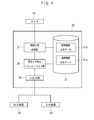
- FIG. 3 is a block diagram showing a configuration of the inspection apparatus 100 according to the embodiment of the present invention.
- the inspection apparatus 100 of this embodiment is an apparatus that inspects display unevenness of a liquid crystal panel.
- the inspection apparatus 100 includes a camera 20 that images a liquid crystal panel, a luminance distribution measuring device 36 that measures a luminance distribution based on image data captured by the camera 20, and a storage device that is connected to the control device 32. 34.
- the storage device 34 has a determination program 35 that determines display unevenness by comparing the luminance distribution data measured by the luminance distribution measuring device 36 with the accumulated luminance distribution data 31a.
- the control device 32 is connected to an accumulated data storage device 38 in which accumulated luminance distribution data (accumulated luminance distribution data) 31a is stored, and the accumulated luminance distribution data 31a is a display unevenness determination result after the mounting process. Contains data.
- the camera 20 of this embodiment is, for example, a CCD image sensor or a CMOS image sensor.
- the control device 32 of the present embodiment is formed of a semiconductor integrated circuit, and is, for example, an MPU (micro processing unit) or a CPU (central processing unit).
- the control device 32 can control the operation of the camera 20 and output image data captured by the camera 20 to the luminance distribution measurement device 36.
- the control device 32 can also output data from the luminance distribution measuring device 36 to the storage device 34 and / or the stored data storage device 38.
- the storage device 34 of this embodiment is, for example, a hard disk (HDD), a semiconductor memory, an optical disk, a magneto-optical disk, or the like.
- the storage device 34 of this embodiment stores a determination program 35 (display unevenness determination program) for determining display unevenness, but other programs, data, and the like can be stored.
- the luminance distribution measuring device 36 is constructed from a program that measures the luminance distribution based on the image data captured by the camera 20, the luminance distribution measuring program can be stored in the storage device 34.
- the stored data storage device 38 of this embodiment is constructed from the same members as the storage device 34, and is, for example, a hard disk (HDD), a semiconductor memory, or the like.
- the accumulated data storage device 38 is formed in a part of the storage device 34.
- the storage device 34 is a hard disk
- the accumulated data storage device 38 is constructed in a part of the hard disk.
- the storage device 34 and the stored data storage device 38 can be constructed by different devices without being constructed by the same device.
- the stage 32 on which the liquid crystal panel for inspection is mounted is connected to the control device 32 of the present embodiment, and the movement of the stage 22 can be controlled by the control device 32.
- the stage 22 may be one that can support and move the liquid crystal panel by a conveyor type (roller conveyor, belt conveyor) in addition to a structure that can support the liquid crystal panel with pins.
- an input device 42 keyboard, mouse, touch panel, etc.
- an output device 44 display, etc.
- a general-purpose PC personal computer
- the display unevenness determination device 30 can be constructed by the control device 32, the luminance distribution measurement device 36, the storage device 34, and the accumulated data storage device 38 of the present embodiment.
- the display unevenness determination device 30 When the display unevenness determination device 30 is constructed from the control device 32, the luminance distribution measurement device 36, the storage device 34, and the accumulated data storage device 38, the configuration shown in FIG.
- the display unevenness determination device 30 shown in FIG. 4 includes a luminance distribution processing unit 37 that performs a luminance distribution process, a display unevenness determination simulation unit 39 that performs display unevenness determination, and a storage unit that stores standard luminance distribution data 31b. 31.
- the luminance distribution processing unit 37 is constructed by the luminance distribution measuring program for constructing the luminance distribution measuring device 36, the control device 32, and the storage device 34 operating in cooperation.
- the display unevenness determination simulation unit 39 is constructed by the display unevenness determination program 35 stored in the storage device 34 and the control device 32 operating in cooperation.
- the storage unit 31 is constructed from a storage device 34 and an accumulated data storage device 38.
- the storage unit 31 stores accumulated luminance distribution data 31a.
- the storage unit 31 also stores standard luminance distribution data 31b indicating inspection result data of a non-defective liquid crystal panel.
- the display unevenness determination device 30 of the present embodiment is connected to the camera 20. Specifically, the luminance distribution processing unit 37 is connected to the camera 20. Further, the luminance distribution processing unit 37, the display unevenness determination simulation unit 39, and the storage unit 31 are connected to each other.
- the display unevenness determination device 30 is provided with an input / output unit (interface) 33, and an input device 42 and an output device 44 are connected via the input / output unit 33.
- the operator can issue an instruction to the luminance distribution processing unit 37, the display unevenness determination simulation unit 39, and / or the camera 20 by the input device 42 of the present embodiment.
- the output device 44 includes image data of the camera 20, an output result (luminance distribution data) of the luminance distribution processing unit 37, an output result (determination result) of the display unevenness determination simulation unit 39, various data 31a in the storage unit 31, 31b or the like can be displayed.
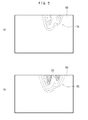
- FIG. 5A shows an example of the luminance distribution 51 of the liquid crystal panel 50.
- the liquid crystal panel 50 shown in FIG. 5A is before the drive circuit is attached.
- a point defect is not found in the liquid crystal panel 50, and the display unevenness evaluated from the luminance distribution 51 is within the allowable range as a good product. Therefore, like the liquid crystal panel 300 shown in FIG. 2A, it is determined that the product is non-defective in this state.
- the liquid crystal panel 50 shown in FIG. 5B shows a luminance distribution 52 after the drive circuit is attached.
- the luminance distribution 52 shown in FIG. 5B has a wider distribution range expressed by luminance mapping than the luminance distribution 51 shown in FIG.
- the luminance distribution 52 illustrated in FIG. 5B includes a region 53 that is evaluated as a defective product as display unevenness.
- the luminance distribution 51 of the liquid crystal panel 50 shown in FIG. 5A is obtained by imaging the liquid crystal panel 50 with the camera 20 and using the image data of the liquid crystal panel 50 as the luminance distribution measuring device 36 (or luminance distribution processing). And a luminance distribution display by processing by the unit 37).
- the liquid crystal panel 50 to be inspected is placed on the stage 22 and the camera 20 images the liquid crystal panel 50.
- the luminance distribution 52 of the liquid crystal panel 50 shown in FIG. 5B is obtained by taking an image of the liquid crystal panel 50 after the drive circuit is attached with the camera 20 and measuring the image data of the liquid crystal panel 50 with the luminance distribution measurement. This is processed by the device 36 (or the luminance distribution processing unit 37) to display the luminance distribution.
- the data of the luminance distribution (51, 52) before and after the drive circuit is attached is accumulated and stored as accumulated luminance distribution data 31a in the accumulated data storage device 38.
- the accumulated luminance distribution data 31a includes display unevenness determination result data after the mounting process. Specifically, determination result data indicating that the luminance distribution 51 is good and the luminance distribution 52 is defective, or the luminance distribution 51 is good and the luminance distribution 52 is also good is added to the accumulated luminance distribution data 31a.
- the pairs of the luminance distribution 51 before installation of the drive circuit and the luminance distribution 52 after installation of the drive circuit are aggregated and accumulated. A certain tendency can be derived.
- the accumulated luminance distribution data 31a if the luminance distribution (51, 52) is accumulated at a predetermined value (for example, at least 10, preferably 50 or more), it can be used effectively.
- the evaluation must be changed to a defective product.
- the standard (threshold value) of cell thickness unevenness 8% can be changed to less than 8% (for example, 6%).
- data of display unevenness (brightness distributions 51 and 52) in the upper right of the liquid crystal panel 50 are totalized and accumulated.
- the display unevenness occurring at the same position can often lead to the same tendency when statistically processed. Therefore, the accumulated data (accumulated luminance distribution data) 31a is used as the presence or absence of display unevenness after the mounting process. It is used as a judgment index for detecting.
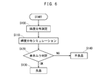
- FIG. 6 is a flowchart for explaining the inspection method of the present embodiment.
- the liquid crystal panel 50 to be inspected is placed on the stage 22, and the liquid crystal panel 50 is imaged by the camera 20.
- the liquid crystal panel 50 is lit in gray (intermediate color) or white and is imaged by the camera 50.
- the luminance distribution of the liquid crystal panel 50 is measured (step S100).
- the luminance distribution is measured by the luminance distribution processing unit 37, the luminance is obtained for each coordinate from the image data of the camera 20, and the luminance distribution is displayed based on the luminance (see “51” in FIG. 5A). Convert to
- Step S110 is a luminance distribution simulation process for estimating the luminance distribution (51) before the mounting process to the luminance distribution (52) after the mounting process.
- the display unevenness determination simulation unit 39 compares the luminance distribution (51) obtained by the luminance distribution processing unit 37 with the accumulated luminance distribution data 31a in the storage unit 31. First, the display unevenness determination simulation unit 39 searches the accumulated luminance distribution data 31a for a pattern having the same type as the luminance distribution (51). If the result of the search is that of the same type of pattern in the accumulated luminance distribution data 31a, display unevenness determination is executed (step S120).
- step S120 the determination result included in the accumulated luminance distribution data 31a of the same pattern is used as the determination result of the liquid crystal panel 50 to be inspected. That is, if the determination result included in the accumulated luminance distribution data 31a of the same pattern is a non-defective product, the determination result of the liquid crystal panel 50 is determined to be a good product (step S130). Alternatively, if the determination result included in the accumulated luminance distribution data 31a of the same pattern is a defective product, the determination result of the liquid crystal panel 50 is determined to be a defective product (step S140).
- step S110 if there is no similar pattern to the luminance distribution (51) in the accumulated luminance distribution data 31a, a search is made as to whether there is a similar pattern that is not the same type pattern. If a similar pattern exists, the display unevenness determination simulation unit 39 corrects the luminance distribution (52) in the similar pattern while referring to the other accumulated luminance distribution data 31a, and the luminance before the mounting process. From the distribution (51), the luminance distribution (52) after the mounting process is calculated.
- the luminance distribution (52) after the mounting process calculated by the display unevenness determination simulation unit 39 is compared with the standard luminance distribution data 31b stored in the storage unit 31, and the display unevenness determination is executed based on the comparison.
- the standard luminance distribution data 31b includes data (threshold value) that is a criterion for determining whether the luminance distribution 52 is a good product or a defective product.
- the display unevenness determination it is determined whether the liquid crystal panel 50 to be inspected is a non-defective product (S130) or a defective product (S140).
- step S110 when the accumulated luminance distribution data 31a has neither the same type pattern nor the similar pattern as the luminance distribution (51), the display unevenness determination simulation unit 39 performs the accumulated luminance distribution data 31a (that is, a large number of patterns). The process of creating a composite pattern from the accumulated data) is executed.
- the composite pattern is created by increasing the cell thickness unevenness by a predetermined percentage or by a predetermined numerical value when the luminance distribution 51 is changed to the luminance distribution 52. (For example, 2% plus calculation).
- the composite pattern can be created by collecting data of display unevenness in the upper right of the liquid crystal panel 50 and using a statistical numerical value such as an average value.
- the mode value may be used.
- the composite pattern calculated by the display unevenness determination simulation unit 39 (the calculated luminance distribution after the mounting process (52)) is compared with the standard luminance distribution data 31b, and display unevenness determination is executed based on the comparison.
- the standard luminance distribution data 31b includes data (threshold value) that is a criterion for determining whether the luminance distribution 52 is a good product or a defective product.
- the display unevenness determination (S120) it is determined whether the liquid crystal panel 50 to be inspected is a non-defective product (S130) or a defective product (S140).
- the liquid crystal panel 50 that has performed the display unevenness determination (S120) through the process of the similar pattern and the composite pattern is again subjected to the non-defective / defective product in the display unevenness inspection after the mounting process that is actually performed in the subsequent process.
- the result will be shown.
- the result of the liquid crystal panel 50 is added to the accumulated luminance distribution data 31a, and the accumulated luminance distribution data 31a is enriched.
- the same pattern range or similar pattern range may be appropriately set according to the actual production line conditions and the liquid crystal panel 50 conditions.
- the standard luminance distribution data 31b can be changed in accordance with the accuracy of the accumulated luminance distribution data 31a and / or the accuracy of the similar pattern / composite pattern calculated by the display unevenness determination simulation unit 39. is there.
- the inspection apparatus 100 of this embodiment includes the control device 32 that controls the camera 20 that images the liquid crystal panel 50, the luminance distribution measurement device 36 that measures the luminance distribution (51), and the luminance distribution data ( 51) and the stored luminance distribution data 31a, and a storage device 34 having a determination program 35 for determining display unevenness. Since the accumulated luminance distribution data 31a includes display unevenness determination result data after the mounting process, the determination program 35 causes the display unevenness after the drive circuit to be attached in the pre-inspection for attaching the drive circuit. It becomes possible to detect the mode.
- the luminance distribution (51) is measured by the luminance distribution processing unit 37 (step S100), and then the luminance distribution 51 and the accumulated luminance distribution data 31a are displayed by the display unevenness determination simulation unit 39. Contrast (step S110).
- step S110 it is possible to detect the presence or absence of display unevenness after the mounting process, although it is an inspection before the mounting process (step S120). If the drive circuit must be attached to the defective liquid crystal panel 50 and inspected, the drive circuit and its mounting process are wasted, resulting in a decrease in throughput and cost. Such a problem can be avoided in the method of the present embodiment.
- an inspection device or an inspection method capable of detecting a defective mode of display unevenness at a stage prior to inspection for attaching a drive circuit.
- SYMBOLS 11 Scan signal wiring 11a Short ring 12 Image signal wiring 12a Short ring 13 Pixel electrode 15 Counter electrode 16 Additional capacity 20 Camera 22 Stage 30 Display unevenness determination apparatus 31 Memory
Landscapes
- Physics & Mathematics (AREA)
- Nonlinear Science (AREA)
- Engineering & Computer Science (AREA)
- Manufacturing & Machinery (AREA)
- Chemical & Material Sciences (AREA)
- Crystallography & Structural Chemistry (AREA)
- General Physics & Mathematics (AREA)
- Optics & Photonics (AREA)
- Liquid Crystal (AREA)
Abstract
駆動回路を取り付ける検査の前段階にて、表示ムラの不良モードを検知できる検査装置を提供する。液晶パネル50の表示ムラを検査する検査装置100であり、液晶パネル50を撮像するカメラ20と、カメラ20を制御する制御装置32と、カメラ20が撮像した画像データに基づいて、輝度分布を測定する輝度分布測定装置36と、制御装置32に接続された記憶装置34とを備える。記憶装置34は、輝度分布データと、蓄積された輝度分布データとを対比することによって、表示ムラを判定する判定プログラム35を有する。制御装置32には、蓄積された輝度分布データが格納された蓄積データ保存装置38が接続されており、蓄積された輝度分布データは、実装工程後における表示ムラの判定結果データを含んでいる。
Description
本発明は、液晶パネルの検査装置および検査方法に関する。特に、液晶パネルの表示ムラを検査する検査装置および検査方法に関する。
なお、本出願は2011年2月25日に出願された日本国特許出願2011-39422号に基づく優先権を主張しており、その出願の全内容は本明細書中に参照として組み入れられている。
なお、本出願は2011年2月25日に出願された日本国特許出願2011-39422号に基づく優先権を主張しており、その出願の全内容は本明細書中に参照として組み入れられている。
液晶表示装置(LCD)の構成部品である液晶パネルは、一対のガラス基板を所定のギャップを確保した状態で対向させた構造を有している。液晶パネルの製造工程においては、まず、アレイ側のガラス基板(マザーガラス)と、カラーフィルタ側のガラス基板(マザーガラス)がそれぞれ別々の工程で加工が行われる。
アレイ側のガラス基板においては、成膜工程とフォトリソグラフィ工程とエッチング工程とが繰り返され(TFTアレイ工程)、薄膜トランジスタ(TFT)、透明電極、それらを繋ぐ配線などを形成した後、最後に配向膜処理を行う。なお、カラーフィルタ側の加工については省略する。セル工程に入ると、アレイ側のガラス基板とカラーフィルタ側のガラス基板との間に、スペーサを介して、液晶材料を注入する。その後は、それぞれのパネルサイズに切り分けた後、偏光板等のフィルムを接着する。このようにして液晶パネルが製造される。
液晶パネルの検査には、その製造工程において大別して2つの機能検査がある。1つはアレイ工程の最終に行う検査である。この検査は、ガラス基板上に作製されたTFT回路の機能、および、短絡を検査するものである。もう一方は、セル工程の最終に行う検査である。この検査は、液晶を封入したパネル(アレイ基板)を点灯させて、テストパターンを表示させることによって、パネルの動作状態を確認するものである。この検査は、点灯検査とも呼ばれ、色度、色ムラ、パネルの動作状態を確認するものである。
上述のように、液晶パネルが製造されたときには、液晶パネルの欠陥検査が行われる。図1を参照しながら、液晶パネルの欠陥検査について説明する(例えば、特許文献1参照)。
図1は、液晶パネル200の等価回路図を示している。図1に示した液晶パネル200では、複数の走査信号配線11と画像信号配線12とがマトリックス状に設けられている。走査信号配線11と画像信号配線12との各交点に画素電極13を設ける。この画素電極13と画像信号配線12にソース・ドレイン端子が接続されると共に、走査信号配線11にゲート端子が接続されたスイッチング用トランジスタ(TFT)14を設ける。そして、この画素電極13と対向電極15との間には、電荷保持用の付加容量16を設けている。
このような液晶パネル200では、駆動回路(不図示)を走査信号配線11および画像信号配線12の端子に接続する前に、正常に動作するか否かを検査する。このような検査を行うに際しては、複数の走査信号配線11を短絡環11aで短絡接続するとともに、複数の画像信号配線12を短絡環12aで短絡接続する。そして、この複数の走査信号配線11と複数の画像信号配線12に、走査信号VGと画像信号VSを供給することによって、全点灯試験を行っていた。
この液晶パネル200の検査では、簡便な検査用配線および端子にて、点欠陥、および、白・黒・グレーの表示ムラを検査することができる。すなわち、図1に示した構造200では、全ての画像信号配線(ソース配線)12を短絡環12aにて短絡接続しているので、全ての絵素領域(またはサブ画素領域)を一度に点灯させて検査することができるので便利である。
しかしながら、駆動回路を取り付ける前の検査では、良品と判定された表示ムラが、駆動回路を実装した後の検査で不良品と判定されるケースが発生する。一例を挙げると、図2(a)に示すように、所定の液晶パネル(例えば、40インチの液晶パネル)300において、駆動回路を取り付ける前の検査では、表示ムラ310(例えば、セル厚ムラが8%)が存在していた。この表示ムラ310は許容できる程度のものであったので、液晶パネル300を良品として判断していた。それが、図2(b)に示すように、駆動回路を実装した後の検査では、不良品と判定される表示ムラ320になることがある。これは、駆動回路を実装した後の検査では、偏光板を貼る工程が加わるなどして、液晶パネル300の状態が変化したことに起因すると推測される。
このように、駆動回路を実装する前の検査で良品と判定された液晶パネル300が、駆動回路を実装した後の検査では不良品と判定されることは問題である。具体的には、不良品の液晶パネル300に対して行った駆動回路の実装工程が無駄になる。駆動回路を実装する前の検査において、そのような不良モード(表示ムラ)を発見できれば、製造工程のスループットの向上にも繋がり、そして、製造コストの低下にもなる。
本発明はかかる点に鑑みてなされたものであり、その主な目的は、駆動回路を取り付ける検査の前段階にて、表示ムラの不良モードを検知することができる検査装置または検査方法を提供することになる。
本発明に係る検査装置は、液晶パネルの表示ムラを検査する検査装置であり、液晶パネルを撮像するカメラと、前記カメラを制御する制御装置と、前記カメラが撮像した画像データに基づいて、輝度分布を測定する輝度分布測定装置と、前記制御装置に接続された記憶装置とを備え、前記記憶装置は、前記輝度分布測定装置が測定した輝度分布と、蓄積された輝度分布データとを対比することによって、表示ムラを判定する判定プログラムを有しており、前記制御装置には、前記蓄積された輝度分布データが格納された蓄積データ保存装置が接続されており、前記蓄積された輝度分布データは、実装工程後における表示ムラの判定結果データを含んでいる。
ある好適な実施形態において、前記制御装置、前記輝度分布測定装置、前記記憶装置および前記蓄積データ保存装置は、表示ムラ判定装置を構築しており、前記表示ムラ判定装置は、前記カメラに接続され、前記輝度分布の処理を行う輝度分布処理部と、前記輝度分布処理部に接続され、前記表示ムラの判定を行う表示ムラ判定シミュレーション部と、前記表示ムラ判定シミュレーション部に接続され、前記蓄積された輝度分布データが格納された記憶部とから構成されている。
本発明に係る検査方法は、液晶パネルの検査方法であり、液晶パネルの輝度分布を測定する工程と、前記輝度分布と、蓄積された輝度分布データとを対比する工程と、前記対比工程によって、実装工程後における表示ムラの有無を検出する工程とを含み、前記対比工程における前記蓄積された輝度分布データは、実装工程後における表示ムラの判定結果データを含んでいる。
本発明によれば、液晶パネルを撮像するカメラを制御する制御装置と、輝度分布を測定する輝度分布測定装置と、輝度分布データと蓄積された輝度分布データとを対比することによって表示ムラを判定する判定プログラムを有する記憶装置とを備えている。蓄積された輝度分布データは、実装工程後における表示ムラの判定結果データを含んでいるので、表示ムラを判定する判定プログラムによって、駆動回路を取り付ける検査の前段階にて、駆動回路を取り付けた後における表示ムラの不良モードを検知することが可能となる。
以下、図面を参照しながら、本発明の実施形態を説明する。以下の図面においては、説明の簡潔化のために、実質的に同一の機能を有する構成要素を同一の参照符号で示す。なお、本発明は以下の実施形態に限定されない。
図3は、本発明の実施形態に係る検査装置100の構成を示すブロック図である。本実施形態の検査装置100は、液晶パネルの表示ムラを検査する装置である。
本実施形態の検査装置100は、液晶パネルを撮像するカメラ20と、カメラ20が撮像した画像データに基づいて、輝度分布を測定する輝度分布測定装置36と、制御装置32に接続された記憶装置34とを備えている。記憶装置34は、輝度分布測定装置36が測定した輝度分布データと、蓄積された輝度分布データ31aとを対比することによって、表示ムラを判定する判定プログラム35を有している。制御装置32には、蓄積された輝度分布データ(蓄積輝度分布データ)31aが格納された蓄積データ保存装置38が接続されており、蓄積輝度分布データ31aは、実装工程後における表示ムラの判定結果データを含んでいる。
本実施形態のカメラ20は、例えば、CCDイメージセンサ、または、CMOSイメージセンサなどである。本実施形態の制御装置32は、半導体集積回路からなり、例えばMPU(マイクロ・プロセッシング・ユニット)またはCPU(セントラル・プロセッシング・ユニット)である。制御装置32は、カメラ20の動作を制御するとともに、カメラ20が撮像した画像データを輝度分布測定装置36に出力することができる。また、制御装置32は、輝度分布測定装置36からのデータを、記憶装置34および/または蓄積データ保存装置38に出力することもできる。
本実施形態の記憶装置34は、例えば、ハードディスク(HDD)、半導体メモリ、光ディスク、光磁気ディスクなどである。本実施形態の記憶装置34には、表示ムラを判定する判定プログラム(表示ムラ判定プログラム)35が格納されているが、他のプログラム、データなどを格納しておくことができる。また、輝度分布測定装置36が、カメラ20が撮像した画像データに基づいて輝度分布を測定するプログラムから構築されている場合、その輝度分布測定プログラムを記憶装置34に格納しておくことができる。
本実施形態の蓄積データ保存装置38は、記憶装置34と同じ部材から構築されており、例えば、ハードディスク(HDD)、半導体メモリなどである。また、本実施形態の構成では、蓄積データ保存装置38は、記憶装置34の一部に形成されており、記憶装置34がハードディスクの場合、そのハードディスクの一部に蓄積データ保存装置38が構築される。なお、記憶装置34と、蓄積データ保存装置38とを同じ装置で構築しなくても、別の装置で構築することも勿論可能である。
本実施形態の制御装置32には、検査用の液晶パネルが載置されるステージ22が接続されており、制御装置32によってステージ22の移動を制御することができる。ステージ22は、液晶パネルをピンで支持できる構成のものの他、コンベア形式(ローラコンベア、ベルトコンベア)にて液晶パネルを支持・移動できるものであってもよい。
さらに、制御装置32には、入力装置42(キーボード、マウス、タッチパネルなど)および出力装置44(ディスプレイなど)が接続されている。本実施形態の制御装置32、記憶装置34、入力装置42、出力装置44は、汎用のPC(パーソナル・コンピュータ)のものを適用することができる。また、本実施形態の制御装置32、輝度分布測定装置36、記憶装置34および蓄積データ保存装置38によって、表示ムラ判定装置30を構築することができる。
制御装置32、輝度分布測定装置36、記憶装置34および蓄積データ保存装置38から、表示ムラ判定装置30を構築した場合、図4に示した構成にすることができる。図4に示した表示ムラ判定装置30は、輝度分布の処理を行う輝度分布処理部37と、表示ムラの判定を行う表示ムラ判定シミュレーション部39と、標準輝度分布データ31bが格納された記憶部31とを含んでいる。
輝度分布処理部37は、輝度分布測定装置36を構築する輝度分布測定プログラムと、制御装置32および記憶装置34が協働して動作することによって構築されている。表示ムラ判定シミュレーション部39は、記憶装置34に格納された表示ムラ判定プログラム35と制御装置32とが協働して動作することによって構築されている。
また、記憶部31は、記憶装置34および蓄積データ保存装置38から構築されている。記憶部31には、蓄積輝度分布データ31aが格納されている。また、本実施形態の構成では、記憶部31には、良品の液晶パネルの検査結果データを示す標準輝度分布データ31bも格納されている。
本実施形態の表示ムラ判定装置30は、カメラ20に接続されている。具体的には、輝度分布処理部37がカメラ20に接続されている。また、輝度分布処理部37、表示ムラ判定シミュレーション部39、記憶部31は、相互に接続されている。表示ムラ判定装置30には、入出力部(インターフェイス)33が設けられており、入出力部33を介して入力装置42、出力装置44が接続されている。
本実施形態の入力装置42によって操作者は、輝度分布処理部37、表示ムラ判定シミュレーション部39及び/又はカメラ20に指示を出すことができる。また、出力装置44には、カメラ20の画像データ、輝度分布処理部37の出力結果(輝度分布データ)、表示ムラ判定シミュレーション部39の出力結果(判定結果)、記憶部31の各種データ31a、31bなどを表示することができる。
図5(a)は、液晶パネル50の輝度分布51の一例を示している。図5(a)に示した液晶パネル50は、駆動回路を取り付ける前のものである。液晶パネル50には点欠陥は発見されず、輝度分布51から評価した表示ムラは、良品として許容範囲のものである。したがって、図2(a)に示した液晶パネル300と同様に、これだけの状態では良品と判断されるものである。
一方、図5(b)に示した液晶パネル50は、駆動回路を取り付けた後における輝度分布52を示している。図5(b)に示した輝度分布52は、図5(a)に示した輝度分布51と比較して、輝度のマッピングによって表現される分布の範囲が広がっている。また、図5(b)に示した輝度分布52には、表示ムラとして不良品として評価される領域53も含まれている。
同じ液晶パネル50であっても、駆動回路を取り付けた前と後で輝度分布(51、52)の差異が出る正確な理由はわからない。おそらく、偏光板を取り付ける工程、駆動回路(不図示)を液晶パネルに実装する工程を通じて、輝度分布の変化が生じるに至ったと推測される。そして、駆動回路を取り付けた前と後で輝度分布(51、52)の変化の傾向を集計して蓄積すると、駆動回路を取り付けた後において、表示ムラが強くなるような輝度分布(一例では、領域53を含むような輝度分布52)が示される。
ここで、図5(a)に示した液晶パネル50の輝度分布51は、カメラ20にて液晶パネル50を撮像し、その液晶パネル50の画像データを、輝度分布測定装置36(または輝度分布処理部37)によって処理して輝度分布表示にしたものである。検査対象の液晶パネル50は、ステージ22の上に載置され、その液晶パネル50をカメラ20が撮像する。同様に、図5(b)に示した液晶パネル50の輝度分布52は、駆動回路を取り付けた後の液晶パネル50をカメラ20にて撮像し、当該液晶パネル50の画像データを、輝度分布測定装置36(または輝度分布処理部37)によって処理して輝度分布表示にしたものである。
本実施形態の構成では、駆動回路の取付け前と後の輝度分布(51、52)のデータを蓄積しておき、蓄積データ保存装置38内に蓄積輝度分布データ31aとして格納しておく。蓄積輝度分布データ31aは、実装工程後における表示ムラの判定結果データを含んでいる。具体的には、輝度分布51が良品で輝度分布52が不良品、あるいは、輝度分布51が良品で輝度分布52も良品の判定結果データが、蓄積輝度分布データ31a内に付け加わっている。
同一機種の液晶パネル50の場合、同一の製造ラインで製造されているときには、駆動回路の取付前の輝度分布51と、駆動回路の取付後の輝度分布52とのペアを集計して蓄積していくと、一定の傾向を導き出すことができる。蓄積輝度分布データ31aでは、輝度分布(51、52)が所定値(例えば、少なくとも10個、好ましくは50個以上)蓄積されたならば、有効に利用することができる。
例えば、輝度分布51の状態においてセル厚ムラが8%存在する場合に良品としていたのに、輝度分布52の状態では不良品に評価を変更しなければならない場合、蓄積輝度分布データ31aに基づきながら、セル厚ムラ8%の基準(閾値)を、8%未満(例えば、6%)に変更することができる。あるいは、図5(a)及び(b)に示すように、液晶パネル50の右上に表示ムラ(輝度分布51、52)が発生しているもののデータを集計して蓄積する。同様の位置に発生した表示ムラは、統計学的に処理した場合、同様の傾向を導き出すことができることが多いので、その蓄積データ(蓄積輝度分布データ)31aを、実装工程後における表示ムラの有無を検出する判定指標に使用する。
次に、図6を参照しながら、本実施形態の検査方法の一例を説明する。図6は、本実施形態の検査方法を説明するためのフローチャートである。
まず、検査する液晶パネル50をステージ22の上に載置して、カメラ20によって液晶パネル50を撮像する。本実施形態では、液晶パネル50は、グレー(中間色)又は白にて点灯し、カメラ50にて撮像する。次に、液晶パネル50の輝度分布を測定する(ステップS100)。輝度分布の測定は、輝度分布処理部37によって実行し、カメラ20の画像データから座標ごとに輝度を求め、その輝度に基づいて輝度分布の表示(図5(a)中の「51」参照)に変換する。
次に、輝度分布処理部37で得られた輝度分布(51)と、記憶部31に格納され蓄積輝度分布データ31aとを対比する(ステップS110)。ステップS110は、実装工程前における輝度分布(51)から、実装工程後の輝度分布(52)への推測を行う輝度分布シミュレーション工程である。
具体的には、表示ムラ判定シミュレーション部39によって、輝度分布処理部37で得られた輝度分布(51)と、記憶部31内の蓄積輝度分布データ31aとを対比する。まず、表示ムラ判定シミュレーション部39は、蓄積輝度分布データ31aから、輝度分布(51)と同種パターンのものが存在するかをサーチする。サーチの結果、同種パターンのものが蓄積輝度分布データ31aにあれば、表示ムラ判定を実行する(ステップS120)。
具体的には、ステップS120において、当該同種パターンの蓄積輝度分布データ31aに含まれている判定結果を、検査対象の液晶パネル50の判定結果にする。すなわち、当該同種パターンの蓄積輝度分布データ31aに含まれている判定結果が良品であれば、液晶パネル50の判定結果を良品にする(ステップS130)。あるいは、当該同種パターンの蓄積輝度分布データ31aに含まれている判定結果が不良品であれば、液晶パネル50の判定結果を不良品にする(ステップS140)。
ステップS110において、蓄積輝度分布データ31aに、輝度分布(51)と同種パターンのものが存在しない場合には、当該同種パターンではないが、類似パターンが存在するかをサーチする。そして、類似パターンが存在する場合、表示ムラ判定シミュレーション部39は、他の蓄積輝度分布データ31aを参照しながら、その類似のパターンにおける輝度分布(52)を補正していき、実装工程前の輝度分布(51)から、実装工程後の輝度分布(52)を算出する。
表示ムラ判定シミュレーション部39にて算出された実装工程後の輝度分布(52)は、記憶部31に格納されている標準輝度分布データ31bと対比されて、その対比によって、表示ムラ判定を実行する(ステップS120)。標準輝度分布データ31bには、輝度分布52が良品であるか不良品であるかの判断基準となるデータ(閾値)が含まれている。表示ムラ判定(S120)の結果、検査対象の液晶パネル50を良品(S130)にするか、不良品(S140)にするかが決定される。
ステップS110において、蓄積輝度分布データ31aに、輝度分布(51)と同種パターンのものも類似パターンのものも存在しない場合には、表示ムラ判定シミュレーション部39が、蓄積輝度分布データ31a(すなわち、多数の蓄積データ)から合成パターンを作成する工程を実行する。
この合成パターンの作成は、例えば、蓄積輝度分布データ31aの統計処理に基づいて、輝度分布51の状態から輝度分布52の状態になると、セル厚ムラが所定割合増加、または、所定数値増加すること(例えば、2%プラスして計算)によって行われる。あるいは、合成パターンの作成は、液晶パネル50の右上に表示ムラが発生しているもののデータを集計して、その平均値などの統計学的な数値を利用することによって行うこともできる。なお、単純な平均値を利用する場合に限らず、集計した所定の上限・下限の値(例えば、上下5%の値)を排除した上で残りのデータの平均値を利用したり、中央値または最頻値を利用したりしても構わない。
ここでも、表示ムラ判定シミュレーション部39で算出した合成パターン(算出された実装工程後の輝度分布(52))は、標準輝度分布データ31bと対比されて、その対比によって、表示ムラ判定を実行する(ステップS120)。標準輝度分布データ31bには、輝度分布52が良品であるか不良品であるかの判断基準となるデータ(閾値)が含まれている。表示ムラ判定(S120)の結果、検査対象の液晶パネル50を良品(S130)にするか、不良品(S140)にするかが決定される。
なお、類似パターン、合成パターンのプロセスを経て表示ムラ判定(S120)を実行した液晶パネル50は、実際に後工程で実行される実装工程後の表示ムラ検査において、再度、その良品・不良品の結果が示されることになる。その液晶パネル50の結果は、蓄積輝度分布データ31aに追加されて、蓄積輝度分布データ31aの充実が図られる。また、同種パターンの範囲、あるいは、類似パターンの範囲は、実際の製造ラインの条件、液晶パネル50の条件に応じて適宜好適なものを設定すればよい。さらに、標準輝度分布データ31bも、蓄積輝度分布データ31aの精度、及び/又は、表示ムラ判定シミュレーション部39によって算出される類似パターン・合成パターンの精度にあわせて、変更していくことも可能である。
以上説明したように、本実施形態の検査装置100は、液晶パネル50を撮像するカメラ20を制御する制御装置32と、輝度分布(51)を測定する輝度分布測定装置36と、輝度分布データ(51)と蓄積輝度分布データ31aとを対比することによって表示ムラを判定する判定プログラム35を有する記憶装置34とを備えている。蓄積輝度分布データ31aは、実装工程後における表示ムラの判定結果データを含んでいるので、判定プログラム35によって、駆動回路を取り付ける検査の前段階にて、駆動回路を取り付けた後における表示ムラの不良モードを検知することが可能となる。
また、本実施形態の手法によれば、輝度分布処理部37によって輝度分布(51)を測定し(ステップS100)、次いで、表示ムラ判定シミュレーション部39によって輝度分布51と蓄積輝度分布データ31aとを対比する(ステップS110)。このステップS110によって、実装工程の前の検査でありながら、実装工程後における表示ムラの有無を検出することができる(ステップS120)。仮に、不良品の液晶パネル50に駆動回路を取り付けて検査しなければならないとすると、駆動回路およびその実装工程が無駄になるため、スループットの低下およびコストの問題が生じる。本実施形態の手法ではそのような問題を回避することができる。
以上、本発明を好適な実施形態により説明してきたが、こうした記述は限定事項ではなく、勿論、種々の改変が可能である。例えば、本実施形態の技術は、大画面液晶パネル(例えば、40インチ以上)に好適に適用できる他、タッチパネル式の液晶パネルにも好適に適用することができる。
本発明によれば、駆動回路を取り付ける検査の前段階にて、表示ムラの不良モードを検知することができる検査装置または検査方法を提供することができる。
11 走査信号配線
11a 短絡環
12 画像信号配線
12a 短絡環
13 画素電極
15 対向電極
16 付加容量
20 カメラ
22 ステージ
30 表示ムラ判定装置
31 記憶部
31a 蓄積輝度分布データ
31b 標準輝度分布データ
32 制御装置
33 入出力部
34 記憶装置
35 表示ムラ判定プログラム
36 輝度分布測定装置
37 輝度分布処理部
38 蓄積データ保存装置
39 表示ムラ判定シミュレーション部
42 入力装置
44 出力装置
50 液晶パネル
51 実装工程前の輝度分布
52 実装工程後の輝度分布
100 検査装置
200 液晶パネル
300 液晶パネル
11a 短絡環
12 画像信号配線
12a 短絡環
13 画素電極
15 対向電極
16 付加容量
20 カメラ
22 ステージ
30 表示ムラ判定装置
31 記憶部
31a 蓄積輝度分布データ
31b 標準輝度分布データ
32 制御装置
33 入出力部
34 記憶装置
35 表示ムラ判定プログラム
36 輝度分布測定装置
37 輝度分布処理部
38 蓄積データ保存装置
39 表示ムラ判定シミュレーション部
42 入力装置
44 出力装置
50 液晶パネル
51 実装工程前の輝度分布
52 実装工程後の輝度分布
100 検査装置
200 液晶パネル
300 液晶パネル
Claims (3)
- 液晶パネルの表示ムラを検査する検査装置であって、
液晶パネルを撮像するカメラと、
前記カメラを制御する制御装置と、
前記カメラが撮像した画像データに基づいて、輝度分布を測定する輝度分布測定装置と、
前記制御装置に接続された記憶装置と
を備え、
前記記憶装置は、前記輝度分布測定装置が測定した輝度分布と、蓄積された輝度分布データとを対比することによって、表示ムラを判定する判定プログラムを有しており、
前記制御装置には、前記蓄積された輝度分布データが格納された蓄積データ保存装置が接続されており、
前記蓄積された輝度分布データは、実装工程後における表示ムラの判定結果データを含んでいる、検査装置。 - 前記制御装置、前記輝度分布測定装置、前記記憶装置および前記蓄積データ保存装置は、表示ムラ判定装置を構築しており、
前記表示ムラ判定装置は、
前記カメラに接続され、前記輝度分布の処理を行う輝度分布処理部と、
前記輝度分布処理部に接続され、前記表示ムラの判定を行う表示ムラ判定シミュレーション部と、
前記表示ムラ判定シミュレーション部に接続され、前記蓄積された輝度分布データが格納された記憶部と
から構成されている、請求項1に記載の検査装置。 - 液晶パネルの検査方法であって、
液晶パネルの輝度分布を測定する工程と、
前記輝度分布と、蓄積された輝度分布データとを対比する工程と、
前記対比工程によって、実装工程後における表示ムラの有無を検出する工程と
を含み、
前記対比工程における前記蓄積された輝度分布データは、実装工程後における表示ムラの判定結果データを含んでいる、検査方法。
Applications Claiming Priority (2)
| Application Number | Priority Date | Filing Date | Title |
|---|---|---|---|
| JP2011039422 | 2011-02-25 | ||
| JP2011-039422 | 2011-02-25 |
Publications (1)
| Publication Number | Publication Date |
|---|---|
| WO2012115003A1 true WO2012115003A1 (ja) | 2012-08-30 |
Family
ID=46720784
Family Applications (1)
| Application Number | Title | Priority Date | Filing Date |
|---|---|---|---|
| PCT/JP2012/053811 Ceased WO2012115003A1 (ja) | 2011-02-25 | 2012-02-17 | 液晶パネルの検査装置および検査方法 |
Country Status (1)
| Country | Link |
|---|---|
| WO (1) | WO2012115003A1 (ja) |
Citations (2)
| Publication number | Priority date | Publication date | Assignee | Title |
|---|---|---|---|---|
| JPH1164810A (ja) * | 1997-08-20 | 1999-03-05 | Sharp Corp | 液晶表示装置の製造方法およびその製造装置 |
| JP2007114660A (ja) * | 2005-10-24 | 2007-05-10 | Optrex Corp | 液晶表示モジュールの製造方法 |
-
2012
- 2012-02-17 WO PCT/JP2012/053811 patent/WO2012115003A1/ja not_active Ceased
Patent Citations (2)
| Publication number | Priority date | Publication date | Assignee | Title |
|---|---|---|---|---|
| JPH1164810A (ja) * | 1997-08-20 | 1999-03-05 | Sharp Corp | 液晶表示装置の製造方法およびその製造装置 |
| JP2007114660A (ja) * | 2005-10-24 | 2007-05-10 | Optrex Corp | 液晶表示モジュールの製造方法 |
Similar Documents
| Publication | Publication Date | Title |
|---|---|---|
| KR101955052B1 (ko) | 전체 원 화상을 사용하여 결함을 검출하는 시스템 및 방법 | |
| TWI442360B (zh) | 顯示器及其接合阻抗的檢測系統以及檢測方法 | |
| CN103809309B (zh) | 基板检测设备及方法 | |
| KR20080098852A (ko) | 얼룩 결함 검사 장치와 방법, 및 평판 디스플레이 패널의제조 방법 | |
| TWI499788B (zh) | 畫素陣列基板檢測方法及畫素陣列基板檢測裝置 | |
| KR20110078958A (ko) | 엘시디 패널 외관 검사장치 | |
| KR102034042B1 (ko) | 평판 디스플레이 패널의 외관 스크래치 검사 방법 | |
| CN111982925A (zh) | 检测方法及检测装置 | |
| KR101374989B1 (ko) | 무라 검출장치 및 그의 구동방법 | |
| CN115167021B (zh) | 显示面板的检测方法及检测装置 | |
| WO2017049863A1 (zh) | 液晶滴注系统及控制方法 | |
| CN115546140A (zh) | 一种显示面板检测方法、系统及电子装置 | |
| KR20080105656A (ko) | 액정 디스플레이 패널의 결함 자동 리페어 장치 및 방법,액정 디스플레이 패널의 제조 방법 | |
| US20120129419A1 (en) | Display-panel inspection method, and method for fabricating display device | |
| WO2017049855A1 (zh) | 显示屏检测方法及设备 | |
| CN107316620B (zh) | 一种显示面板、显示装置和调整显示面板的串扰的方法 | |
| CN112465780B (zh) | 绝缘层膜厚异常监控方法及装置 | |
| CN101354485B (zh) | 显示装置的测试系统及测试方法 | |
| WO2012169423A1 (ja) | パターン検査装置およびパターン検査方法 | |
| KR101738928B1 (ko) | 인셀 타입 터치 센서의 오픈 불량 감지방법 | |
| WO2012115003A1 (ja) | 液晶パネルの検査装置および検査方法 | |
| KR101286548B1 (ko) | 액정표시장치의 검사 시스템 및 방법 | |
| WO2012115004A1 (ja) | 液晶パネルの検査装置および検査方法 | |
| JP2015087529A (ja) | 欠陥検査装置、欠陥検査方法、及び信号入力装置 | |
| TWI282417B (en) | Automated optical inspection method |
Legal Events
| Date | Code | Title | Description |
|---|---|---|---|
| 121 | Ep: the epo has been informed by wipo that ep was designated in this application |
Ref document number: 12750288 Country of ref document: EP Kind code of ref document: A1 |
|
| NENP | Non-entry into the national phase |
Ref country code: DE |
|
| 122 | Ep: pct application non-entry in european phase |
Ref document number: 12750288 Country of ref document: EP Kind code of ref document: A1 |
|
| NENP | Non-entry into the national phase |
Ref country code: JP |