WO2012111558A1 - 液晶表示装置 - Google Patents
液晶表示装置 Download PDFInfo
- Publication number
- WO2012111558A1 WO2012111558A1 PCT/JP2012/053117 JP2012053117W WO2012111558A1 WO 2012111558 A1 WO2012111558 A1 WO 2012111558A1 JP 2012053117 W JP2012053117 W JP 2012053117W WO 2012111558 A1 WO2012111558 A1 WO 2012111558A1
- Authority
- WO
- WIPO (PCT)
- Prior art keywords
- liquid crystal
- slit
- pixel
- display device
- pixels
- Prior art date
- Legal status (The legal status is an assumption and is not a legal conclusion. Google has not performed a legal analysis and makes no representation as to the accuracy of the status listed.)
- Ceased
Links
Images













Classifications
-
- G—PHYSICS
- G02—OPTICS
- G02F—OPTICAL DEVICES OR ARRANGEMENTS FOR THE CONTROL OF LIGHT BY MODIFICATION OF THE OPTICAL PROPERTIES OF THE MEDIA OF THE ELEMENTS INVOLVED THEREIN; NON-LINEAR OPTICS; FREQUENCY-CHANGING OF LIGHT; OPTICAL LOGIC ELEMENTS; OPTICAL ANALOGUE/DIGITAL CONVERTERS
- G02F1/00—Devices or arrangements for the control of the intensity, colour, phase, polarisation or direction of light arriving from an independent light source, e.g. switching, gating or modulating; Non-linear optics
- G02F1/01—Devices or arrangements for the control of the intensity, colour, phase, polarisation or direction of light arriving from an independent light source, e.g. switching, gating or modulating; Non-linear optics for the control of the intensity, phase, polarisation or colour
- G02F1/13—Devices or arrangements for the control of the intensity, colour, phase, polarisation or direction of light arriving from an independent light source, e.g. switching, gating or modulating; Non-linear optics for the control of the intensity, phase, polarisation or colour based on liquid crystals, e.g. single liquid crystal display cells
- G02F1/133—Constructional arrangements; Operation of liquid crystal cells; Circuit arrangements
- G02F1/1333—Constructional arrangements; Manufacturing methods
- G02F1/1343—Electrodes
- G02F1/13439—Electrodes characterised by their electrical, optical, physical properties; materials therefor; method of making
-
- G—PHYSICS
- G02—OPTICS
- G02F—OPTICAL DEVICES OR ARRANGEMENTS FOR THE CONTROL OF LIGHT BY MODIFICATION OF THE OPTICAL PROPERTIES OF THE MEDIA OF THE ELEMENTS INVOLVED THEREIN; NON-LINEAR OPTICS; FREQUENCY-CHANGING OF LIGHT; OPTICAL LOGIC ELEMENTS; OPTICAL ANALOGUE/DIGITAL CONVERTERS
- G02F1/00—Devices or arrangements for the control of the intensity, colour, phase, polarisation or direction of light arriving from an independent light source, e.g. switching, gating or modulating; Non-linear optics
- G02F1/01—Devices or arrangements for the control of the intensity, colour, phase, polarisation or direction of light arriving from an independent light source, e.g. switching, gating or modulating; Non-linear optics for the control of the intensity, phase, polarisation or colour
- G02F1/13—Devices or arrangements for the control of the intensity, colour, phase, polarisation or direction of light arriving from an independent light source, e.g. switching, gating or modulating; Non-linear optics for the control of the intensity, phase, polarisation or colour based on liquid crystals, e.g. single liquid crystal display cells
- G02F1/133—Constructional arrangements; Operation of liquid crystal cells; Circuit arrangements
- G02F1/1333—Constructional arrangements; Manufacturing methods
- G02F1/1337—Surface-induced orientation of the liquid crystal molecules, e.g. by alignment layers
- G02F1/133707—Structures for producing distorted electric fields, e.g. bumps, protrusions, recesses, slits in pixel electrodes
-
- G—PHYSICS
- G02—OPTICS
- G02F—OPTICAL DEVICES OR ARRANGEMENTS FOR THE CONTROL OF LIGHT BY MODIFICATION OF THE OPTICAL PROPERTIES OF THE MEDIA OF THE ELEMENTS INVOLVED THEREIN; NON-LINEAR OPTICS; FREQUENCY-CHANGING OF LIGHT; OPTICAL LOGIC ELEMENTS; OPTICAL ANALOGUE/DIGITAL CONVERTERS
- G02F1/00—Devices or arrangements for the control of the intensity, colour, phase, polarisation or direction of light arriving from an independent light source, e.g. switching, gating or modulating; Non-linear optics
- G02F1/01—Devices or arrangements for the control of the intensity, colour, phase, polarisation or direction of light arriving from an independent light source, e.g. switching, gating or modulating; Non-linear optics for the control of the intensity, phase, polarisation or colour
- G02F1/13—Devices or arrangements for the control of the intensity, colour, phase, polarisation or direction of light arriving from an independent light source, e.g. switching, gating or modulating; Non-linear optics for the control of the intensity, phase, polarisation or colour based on liquid crystals, e.g. single liquid crystal display cells
- G02F1/133—Constructional arrangements; Operation of liquid crystal cells; Circuit arrangements
- G02F1/1333—Constructional arrangements; Manufacturing methods
- G02F1/1337—Surface-induced orientation of the liquid crystal molecules, e.g. by alignment layers
- G02F1/133753—Surface-induced orientation of the liquid crystal molecules, e.g. by alignment layers with different alignment orientations or pretilt angles on a same surface, e.g. for grey scale or improved viewing angle
-
- G—PHYSICS
- G02—OPTICS
- G02F—OPTICAL DEVICES OR ARRANGEMENTS FOR THE CONTROL OF LIGHT BY MODIFICATION OF THE OPTICAL PROPERTIES OF THE MEDIA OF THE ELEMENTS INVOLVED THEREIN; NON-LINEAR OPTICS; FREQUENCY-CHANGING OF LIGHT; OPTICAL LOGIC ELEMENTS; OPTICAL ANALOGUE/DIGITAL CONVERTERS
- G02F1/00—Devices or arrangements for the control of the intensity, colour, phase, polarisation or direction of light arriving from an independent light source, e.g. switching, gating or modulating; Non-linear optics
- G02F1/01—Devices or arrangements for the control of the intensity, colour, phase, polarisation or direction of light arriving from an independent light source, e.g. switching, gating or modulating; Non-linear optics for the control of the intensity, phase, polarisation or colour
- G02F1/13—Devices or arrangements for the control of the intensity, colour, phase, polarisation or direction of light arriving from an independent light source, e.g. switching, gating or modulating; Non-linear optics for the control of the intensity, phase, polarisation or colour based on liquid crystals, e.g. single liquid crystal display cells
- G02F1/133—Constructional arrangements; Operation of liquid crystal cells; Circuit arrangements
- G02F1/1333—Constructional arrangements; Manufacturing methods
- G02F1/1343—Electrodes
- G02F1/134309—Electrodes characterised by their geometrical arrangement
-
- G—PHYSICS
- G02—OPTICS
- G02F—OPTICAL DEVICES OR ARRANGEMENTS FOR THE CONTROL OF LIGHT BY MODIFICATION OF THE OPTICAL PROPERTIES OF THE MEDIA OF THE ELEMENTS INVOLVED THEREIN; NON-LINEAR OPTICS; FREQUENCY-CHANGING OF LIGHT; OPTICAL LOGIC ELEMENTS; OPTICAL ANALOGUE/DIGITAL CONVERTERS
- G02F1/00—Devices or arrangements for the control of the intensity, colour, phase, polarisation or direction of light arriving from an independent light source, e.g. switching, gating or modulating; Non-linear optics
- G02F1/01—Devices or arrangements for the control of the intensity, colour, phase, polarisation or direction of light arriving from an independent light source, e.g. switching, gating or modulating; Non-linear optics for the control of the intensity, phase, polarisation or colour
- G02F1/13—Devices or arrangements for the control of the intensity, colour, phase, polarisation or direction of light arriving from an independent light source, e.g. switching, gating or modulating; Non-linear optics for the control of the intensity, phase, polarisation or colour based on liquid crystals, e.g. single liquid crystal display cells
- G02F1/133—Constructional arrangements; Operation of liquid crystal cells; Circuit arrangements
- G02F1/1333—Constructional arrangements; Manufacturing methods
- G02F1/1337—Surface-induced orientation of the liquid crystal molecules, e.g. by alignment layers
- G02F1/13373—Disclination line; Reverse tilt
-
- G—PHYSICS
- G02—OPTICS
- G02F—OPTICAL DEVICES OR ARRANGEMENTS FOR THE CONTROL OF LIGHT BY MODIFICATION OF THE OPTICAL PROPERTIES OF THE MEDIA OF THE ELEMENTS INVOLVED THEREIN; NON-LINEAR OPTICS; FREQUENCY-CHANGING OF LIGHT; OPTICAL LOGIC ELEMENTS; OPTICAL ANALOGUE/DIGITAL CONVERTERS
- G02F1/00—Devices or arrangements for the control of the intensity, colour, phase, polarisation or direction of light arriving from an independent light source, e.g. switching, gating or modulating; Non-linear optics
- G02F1/01—Devices or arrangements for the control of the intensity, colour, phase, polarisation or direction of light arriving from an independent light source, e.g. switching, gating or modulating; Non-linear optics for the control of the intensity, phase, polarisation or colour
- G02F1/13—Devices or arrangements for the control of the intensity, colour, phase, polarisation or direction of light arriving from an independent light source, e.g. switching, gating or modulating; Non-linear optics for the control of the intensity, phase, polarisation or colour based on liquid crystals, e.g. single liquid crystal display cells
- G02F1/133—Constructional arrangements; Operation of liquid crystal cells; Circuit arrangements
- G02F1/1333—Constructional arrangements; Manufacturing methods
- G02F1/1337—Surface-induced orientation of the liquid crystal molecules, e.g. by alignment layers
- G02F1/133742—Surface-induced orientation of the liquid crystal molecules, e.g. by alignment layers for homeotropic alignment
-
- G—PHYSICS
- G02—OPTICS
- G02F—OPTICAL DEVICES OR ARRANGEMENTS FOR THE CONTROL OF LIGHT BY MODIFICATION OF THE OPTICAL PROPERTIES OF THE MEDIA OF THE ELEMENTS INVOLVED THEREIN; NON-LINEAR OPTICS; FREQUENCY-CHANGING OF LIGHT; OPTICAL LOGIC ELEMENTS; OPTICAL ANALOGUE/DIGITAL CONVERTERS
- G02F1/00—Devices or arrangements for the control of the intensity, colour, phase, polarisation or direction of light arriving from an independent light source, e.g. switching, gating or modulating; Non-linear optics
- G02F1/01—Devices or arrangements for the control of the intensity, colour, phase, polarisation or direction of light arriving from an independent light source, e.g. switching, gating or modulating; Non-linear optics for the control of the intensity, phase, polarisation or colour
- G02F1/13—Devices or arrangements for the control of the intensity, colour, phase, polarisation or direction of light arriving from an independent light source, e.g. switching, gating or modulating; Non-linear optics for the control of the intensity, phase, polarisation or colour based on liquid crystals, e.g. single liquid crystal display cells
- G02F1/137—Devices or arrangements for the control of the intensity, colour, phase, polarisation or direction of light arriving from an independent light source, e.g. switching, gating or modulating; Non-linear optics for the control of the intensity, phase, polarisation or colour based on liquid crystals, e.g. single liquid crystal display cells characterised by the electro-optical or magneto-optical effect, e.g. field-induced phase transition, orientation effect, guest-host interaction or dynamic scattering
- G02F1/139—Devices or arrangements for the control of the intensity, colour, phase, polarisation or direction of light arriving from an independent light source, e.g. switching, gating or modulating; Non-linear optics for the control of the intensity, phase, polarisation or colour based on liquid crystals, e.g. single liquid crystal display cells characterised by the electro-optical or magneto-optical effect, e.g. field-induced phase transition, orientation effect, guest-host interaction or dynamic scattering based on orientation effects in which the liquid crystal remains transparent
- G02F1/1393—Devices or arrangements for the control of the intensity, colour, phase, polarisation or direction of light arriving from an independent light source, e.g. switching, gating or modulating; Non-linear optics for the control of the intensity, phase, polarisation or colour based on liquid crystals, e.g. single liquid crystal display cells characterised by the electro-optical or magneto-optical effect, e.g. field-induced phase transition, orientation effect, guest-host interaction or dynamic scattering based on orientation effects in which the liquid crystal remains transparent the birefringence of the liquid crystal being electrically controlled, e.g. ECB-, DAP-, HAN-, PI-LC cells
-
- G—PHYSICS
- G02—OPTICS
- G02F—OPTICAL DEVICES OR ARRANGEMENTS FOR THE CONTROL OF LIGHT BY MODIFICATION OF THE OPTICAL PROPERTIES OF THE MEDIA OF THE ELEMENTS INVOLVED THEREIN; NON-LINEAR OPTICS; FREQUENCY-CHANGING OF LIGHT; OPTICAL LOGIC ELEMENTS; OPTICAL ANALOGUE/DIGITAL CONVERTERS
- G02F2201/00—Constructional arrangements not provided for in groups G02F1/00 - G02F7/00
- G02F2201/12—Constructional arrangements not provided for in groups G02F1/00 - G02F7/00 electrode
- G02F2201/121—Constructional arrangements not provided for in groups G02F1/00 - G02F7/00 electrode common or background
Definitions
- the present invention relates to a liquid crystal display device.
- the present invention relates to a liquid crystal display device in which a plurality of domains are formed in one pixel.
- various liquid crystal display devices have been proposed, and in recent years, in particular, various liquid crystal display devices with an increased viewing angle, suppression of disclination, and reduction of burn-in have been proposed.
- an MVA (Multidomain Vertical Alignment) method in which a plurality of domains are formed in one pixel has been proposed.
- Patent Document 1 Japanese Patent Laid-Open No. 2007-249243 (Patent Document 1) describes an example of an MVA liquid crystal display device.
- the MVA liquid crystal display device described in Patent Document 1 includes a pair of substrates, a plurality of domains formed in one pixel, and a domain regulating unit that regulates the tilting direction of liquid crystal molecules in each domain.
- domain regulating means protrusions and depressions formed on the surface of the substrate and fishbone-shaped electrodes provided on the substrate are cited.
- the tilt directions of liquid crystal molecules in each domain at the time of voltage application are made different.
- the viewing angle is improved by changing the tilt direction of the liquid crystal molecules in each domain.
- the liquid crystal display device described in Japanese Patent Application Laid-Open No. 2008-197691 includes a domain formed in one pixel and a vertical alignment film provided in a portion in contact with the liquid crystal layer.
- the vertical alignment film is subjected to alignment treatment by irradiating ultraviolet rays (UV: Ultra Violet light) from an oblique direction. Forming a plurality of domains by varying the irradiation direction of the ultraviolet light by the position.
- This liquid crystal display device includes a protruding structure so that liquid crystal molecules are aligned toward the orientation regulating direction of each domain when a voltage is applied.
- liquid crystal display device having a plurality of domains in which liquid crystal molecules have different orientations when a voltage is applied, dark lines are generated in the vicinity of some sections of the boundary between pixels.
- an object of the present invention is to provide a liquid crystal display device having a plurality of domains, in which the width of a dark line generated in the vicinity of a part of a boundary between pixels is reduced. To do.
- a liquid crystal display device has a display region including a plurality of pixels, and is bonded to each other so as to sandwich at least the liquid crystal layer extending in the display region. And a pair of polarizing plates arranged so as to sandwich the first and second substrates.
- a pixel electrode is provided on the first substrate corresponding to each of the plurality of pixels.
- a counter electrode disposed so as to face the pixel electrode.
- the surface of the liquid crystal layer side of the pixel electrode are disposed first alignment film.
- the surface of the liquid crystal layer side of the counter electrode is disposed a second alignment film.
- the pixel includes a plurality of domains in which the combinations of orientation directions of the first and second alignment films are different from each other.
- the counter electrode is provided with a slit in at least a part of a region corresponding to a boundary between adjacent pixels among the plurality of pixels.
- the counter electrode is provided with the slit, the width of the dark line generated in the vicinity of a part of the boundary between the pixels can be reduced.
- FIG. 21 It is the figure which displayed the simulation result shown in FIG. 21 simplified. It is a simulation result of the dark line generation
- FIG. 25 is a plan view of two pixels shown in FIG. 24 arranged on the left and right. It is an enlarged view of the B section in FIG. It is a simulation result of the behavior of the liquid crystal molecule of Example 1 based on the present invention. It is a simulation result of the transmission state of Example 1 based on this invention. It is a simulation result of the behavior of the liquid crystal molecule of Example 2 based on the present invention.
- FIG. 6 is a graph showing a change in overall transmittance when the slit width W is changed over Examples 1 to 5. It is a top view of the 1st example of the counter electrode with which the liquid crystal display device in Embodiment 1 based on this invention is provided. It is a top view of the 2nd example of the counter electrode with which the liquid crystal display device in Embodiment 1 based on this invention is provided.
- a liquid crystal display device having a plurality of domains
- the orientation of liquid crystal molecules is determined for each domain.
- the substrate sandwiching the liquid crystal layer is called a TFT (Thin Film Transistor) substrate and a counter substrate.
- the counter substrate may include a color filter.
- a pixel electrode having the shape shown in FIG. 1 is provided on the surface of the TFT substrate on the liquid crystal layer side. Both the TFT substrate and the counter substrate have an alignment film on the surface in contact with the liquid crystal layer.
- the pixel electrode is covered with an alignment film.
- alignment films are provided on the surfaces of the TFT substrate and the counter substrate, and different alignment directions are set in these alignment films.
- those in the vicinity of the alignment films of the TFT substrate and the counter substrate are inclined according to the alignment direction of the alignment film.
- tilt angle The angle formed by the longitudinal direction of the liquid crystal molecules and the substrate surface is called a “tilt angle”.
- the direction in which the liquid crystal molecules are tilted when viewed from the direction perpendicular to the substrate is referred to as the “tilt direction”.
- tilt angle and tilt azimuth when no voltage is applied to the pixel electrode are referred to as a pretilt angle and a pretilt azimuth, respectively.
- the degree to which the orientation of the liquid crystal molecules is affected by the alignment film decreases as the distance from the alignment film increases along the thickness direction of the liquid crystal layer.
- the tilt azimuth of the liquid crystal molecules changes along the thickness direction.
- the liquid crystal molecules are tilted in a tilt direction corresponding to the average of the tilt direction determined by the alignment film of the TFT substrate and the tilt direction determined by the alignment film of the counter substrate.
- the liquid crystal molecules tend to tilt in the direction perpendicular to the outline of the pixel and toward the inside of the outline due to the influence of the oblique electric field generated by the end of the pixel electrode.
- each pixel a pixel electrode having the shape shown in FIG. 1 is provided on the TFT substrate side. Although a large number of pixels are actually arranged on the substrate, the following description will be made with attention paid to the state in one pixel.
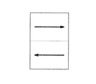
- each pixel is divided into two regions on the left and right, and the alignment film is exposed in the direction set for each region.
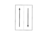
- On the counter substrate each pixel is vertically divided into two regions as shown in FIG. 3, and the alignment film is exposed in the direction set for each region.
- the arrows in FIGS. 2 and 3 indicate the light irradiation direction during exposure.
- the inclination of liquid crystal molecules is shown as a symbol.
- the orientation direction is set to the left as shown by the arrow in FIG. 4 on the upper surface of the substrate and the liquid crystal molecules are tilted
- the liquid crystal molecules in FIG. 4 are viewed from above the substrate. Since the left end of is visible to the observer, the end is displayed with an elliptical head. Since the right end of the liquid crystal molecules in FIG. 4 looks far from the observer, it is displayed with a sharp tail.
- the state of the liquid crystal molecules corresponding to FIG. 4 is displayed in a tadpole shape as shown in FIG.
- the tilt orientation of liquid crystal molecules can be grasped by the head direction of the tadpole.
- the alignment film acquires a certain alignment orientation by exposing from a certain tilt direction with respect to the alignment film.
- the orientation direction is opposite to the exposure direction.
- the orientation film on the surface of the TFT substrate has an orientation orientation as shown in FIG.
- the orientation film on the surface of the counter substrate has an orientation orientation as shown in FIG.
- the arrows in FIGS. 6 and 7 mean the set orientation direction, which means that the orientation film has the property of tilting the liquid crystal molecules in the vicinity of the orientation film in the orientation.
- the TFT substrate shown in FIG. 6 is turned upside down so that the counter substrate shown in FIG. 7 is reversed left and right and is covered from above, and a liquid crystal layer is held between the TFT substrate and the counter substrate.
- the arrow displayed as the vertical arrow is the orientation orientation of the orientation film formed on the upper surface of the TFT substrate.
- the arrows displayed as the left and right arrows are the orientation directions of the alignment film formed on the lower surface of the counter substrate.
- the liquid crystal molecules tilted by the alignment film on the lower surface of the counter substrate are observed by the observer so as to pass through the counter substrate. Since the end of the liquid crystal molecule on the counter substrate side is the end close to the observer, this end is displayed as a tadpole-shaped head.
- FIG. 8 two tadpole shapes indicating liquid crystal molecules are displayed in each domain so as to overlap each other, but the tadpole shape on the front side of the page represents the tilt orientation of the liquid crystal molecules in the vicinity of the counter substrate.
- the tadpole shape on the back side of the paper represents the tilt orientation of the liquid crystal molecules in the vicinity of the TFT substrate.
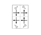
- the tilt azimuth appearing in the liquid crystal molecules near the TFT substrate and the tilt azimuth appearing in the liquid crystal molecules near the counter substrate intersect at 90 °.
- the liquid crystal molecules are tilted in the direction in which the two tilt directions displayed in FIG. 8 are combined. Therefore, the tilt direction of the liquid crystal molecules at the center in the thickness direction in each domain is As shown in FIG.
- a voltage is applied, an oblique electric field is generated near the outline of the pixel electrode provided on the TFT substrate, as shown in FIG. That is, the liquid crystal molecules in the vicinity of the outline of the pixel electrode tend to tilt to the side perpendicular to the outline due to the influence of the oblique electric field.
- the inclination of the liquid crystal molecules is displayed on the outline of the pixel electrode.
- each domain the side that also serves as the outline of the pixel is called a “domain side”.
- Eight domain sides can be assumed in one pixel.
- Each side of the pixel consists of two domain sides.
- the direction of the liquid crystal molecules is disturbed, resulting in dark lines.
- the tilt angle of the liquid crystal molecules is different by 90 °, so that a dark line is generated.
- dark lines are generated at the boundaries between domains and at the four domain sides on the outline of the pixel.
- a dark line appears in the shape of a swastika as a whole of one pixel.
- the simulation results of the transmission state was performed to confirm the occurrence of dark lines shown in FIG. 13.
- FIG. 14 shows the result of overlapping the symbol indicating the liquid crystal molecule and the simulation result of the dark line generation. Dark line is generated in a section surrounded by a dashed ellipse in FIG. 14.
- FIG. 15 shows the inventors' investigation of the behavior of liquid crystal molecules in the liquid crystal layer 4 by simulation.
- a pixel electrode 8 is formed on the upper surface of the TFT substrate 5, and a counter electrode 9 is formed on the lower surface of the counter substrate 6.
- the TFT substrate 5 and the counter substrate 6 are arranged to face each other with the liquid crystal layer 4 interposed therebetween.
- the vicinity of the gap 14 between the pixel electrodes 8 is displayed.
- a large number of pin-shaped figures displayed in the liquid crystal layer 4 indicate the postures of the liquid crystal molecules in each part. However, the tilt may be exaggerated for easy understanding of the orientation in which the liquid crystal molecules tilt.
- a curve 17 displayed on the liquid crystal layer 4 is a graph showing the transmittance of the liquid crystal layer 4 at that portion. According to FIG.
- FIG. 16 shows a simplified version of the simulation result of FIG.
- the liquid crystal molecules 18 are tilted in the correct orientation (hereinafter referred to as “positive orientation”) in the interior of the pixel electrode 8 away from the end of the pixel electrode 8.
- the normal orientation is an orientation that forms 45 ° with respect to the outer side of the pixel electrode 8 in a plan view as shown in the tadpole shape in FIG. As shown in FIGS.
- any liquid crystal molecules in the projection area of the gap 14 have an effect on the influence. is recieving.
- the liquid crystal molecules 19 are inclined in a direction almost opposite to the normal direction (hereinafter referred to as “reverse direction”).
- the orientation of the liquid crystal molecules changes abruptly from the reverse orientation to the positive orientation in a narrow section.
- the simulation result of the transmission state in this part is shown in FIG.
- the center line of the gap between the pixel electrodes 8 is a middle line 16.
- a dark line 20 is generated along the middle line 16, and another dark line 21 is generated on the right side of the dark line 20.
- the dark line 21 in FIG. 17 corresponds to the region 15 in FIGS. 15 and 16.
- the dark line 20 and the dark line 21 can be combined and regarded as a single band-like dark line.
- the inventors have focused on the fact that dark lines are generated according to the principle described above, and have completed the present invention in order to suppress the generation of such dark lines.
- the liquid crystal display device 1 in the present embodiment has a display area 2 including a plurality of pixels 3.
- the liquid crystal display device 1 includes a liquid crystal layer 4 extending at least in the display region 2 and a TFT substrate 5 as a first and second substrate bonded together so as to sandwich the liquid crystal layer 4. And a counter substrate 6 and a pair of polarizing plates 7a and 7b arranged so as to sandwich the first and second substrates.
- the TFT substrate 5 as the first substrate is provided with a pixel electrode 8 corresponding to each of the plurality of pixels 3.
- a counter substrate 9 as the second substrate is provided with a counter electrode 9 so as to face the pixel electrode 8.
- a first alignment film 11 is disposed on the surface of the pixel electrode 8 on the liquid crystal layer 4 side.
- a second alignment film 12 is disposed on the surface of the counter electrode 9 on the liquid crystal layer 4 side.
- the pixel 3 includes a plurality of domains 13 in which the combinations of the orientation directions of the first and second alignment films are different from each other.
- a slit 22 is provided in the counter electrode 9 in at least a part of a region corresponding to the boundary between adjacent pixels 3 among the plurality of pixels 3.
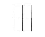
- one pixel 3 includes four domains 13 as illustrated in FIG.
- the pixel electrode 8 and the counter electrode 9 may be made of ITO (Indium Tin Oxide).
- the counter substrate 6 may be a substrate on which a color filter is formed.
- the slit 22 is provided in the counter electrode 9 as described above, so that the width of the dark line generated in the vicinity of a part of the boundary between the pixels can be reduced.
- the inventors performed a simulation. The result is shown in FIG. FIG. 22 shows a simplified version of the simulation result of FIG. FIG. 23 shows the state of dark lines obtained in the liquid crystal display device in this embodiment.
- the counter electrode 9 since the counter electrode 9 is provided with the slit 22, a part of the lines of electric force pass through the slit 22 on the counter substrate 9 side. Since the liquid crystal molecules are tilted along the lines of electric force, so-called alignment loss of the liquid crystal molecules is reduced. As a result, as shown in FIG. 23, the dark lines are combined into one, and the total width of the dark lines generated in the vicinity of the boundary between the pixels is reduced. In FIG. 23, the dark line is not completely extinguished, but the width is clearly smaller than the dark line shown in FIG. Thus, it can be said that it is possible to obtain the effect of suppressing reduce the width of the dark line.
- the slit 22 in the counter electrode 9 does not necessarily match the width of the gap 14 of the pixel electrode 8. As shown in FIG. 22, the slit 22 may be wider than the gap 14. The center line of the slit 22 does not necessarily coincide with the middle line 16 of the gap 14. The slit 22 may be arranged so as to be biased toward the one pixel. As shown in FIG. 17, originally, a dark line was generated at the position where it entered the pixel on the right side. However, in this embodiment, as shown in FIG. 22, the slit 22 is on the side where the dark line was originally generated. They are arranged so as to be biased toward the pixels.
- the slit 22 is provided in a section where a dark line is generated when no slit is provided in the counter electrode 9 in a boundary line between adjacent pixels. This is because the effect of reducing the width of the resulting dark line is particularly increased by adopting such a configuration.
- the slit 22 is the outer side of each of the plurality of domains 13 and also the outer side of each of the plurality of pixels 3, that is, of the domain sides, the pixel electrode 8 and the counter electrode 9.
- the side on the opposite electrode 9 side in the longitudinal direction of the liquid crystal molecules faces. It is preferable to be provided on the side. This is because, based on the principle, dark lines are generated on such sides, and the effect of reducing the width of the generated dark lines is particularly increased by providing slits on such sides.
- a rectangular planar area 23 having a length of 230.75 ⁇ m and a width of 153.75 ⁇ m is assumed as an area corresponding to one pixel, as shown in FIG. It is assumed that the pixel electrode 8 is arranged inside the plane region 23 with a gap of 3 ⁇ m vertically and horizontally. Therefore, the width of the gap 14 between the pixel electrodes 8 is 6 ⁇ m.
- the orientation direction in the orientation film of each substrate was set to the direction indicated by the arrow in FIG. That is, in the counter substrate, the alignment film is divided into two upper and lower regions, and in the TFT substrate, the alignment film is divided into two left and right regions. Two domains are formed.
- the tilt azimuths of the liquid crystal molecules at the center in the thickness direction in each domain are shown in FIG. 10 as four tadpole shapes, respectively.
- the pretilt angle of the liquid crystal molecules was 88.2 ° in both the TFT substrate 5 and the counter substrate 6.
- FIG. 25 shows the two pixels shown in FIG. 24 arranged side by side.
- a dot inversion driving method which is a method often used for liquid crystal display panels currently mass-produced, is assumed, and opposite potentials are applied between adjacent pixel electrodes 8a and 8b.
- the symbols “ ⁇ ” and “+” shown in FIG. 26 mean potentials applied to the pixel electrodes 8a and 8b, respectively.
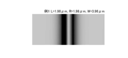
- Example 1 First, as Example 1 based on the present invention, FIGS. 27 and 28 show simulation results when the slit width W is 3.96 ⁇ m by setting L and R to 1.98 ⁇ m.
- Example 1 although slightly improved as compared with the comparative example, the influence of the slit 22 of the counter electrode 9 on the electric field is small, and the behavior of the liquid crystal molecules and the transmission state are only slightly improved compared to the comparative example. I could't see it.
- FIGS. 29 and 30 show simulation results when the slit width W is 9.0 ⁇ m by setting both L and R to 4.5 ⁇ m.
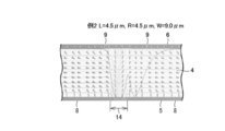
- the lines of electric force change due to the influence of the slit 22 of the counter electrode 9, and the alignment of the liquid crystal molecules changes. Since the lines of electric force at the end of the left pixel electrode 8 have changed upward, the regulation force on the alignment in the left pixel electrode 8 has increased, and the orientation of the liquid crystal molecules that have changed gently in the comparative example has changed. It is changing rapidly. As a result, the transmittance in the vicinity of the end portion of the left pixel electrode 8 is significantly increased as compared with the comparative example.
- FIGS. 31 and 32 show the simulation results when L is 4.5 ⁇ m and R is 5.75 ⁇ m so that the slit width W is 10.25 ⁇ m.
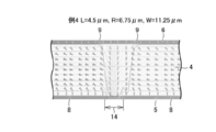
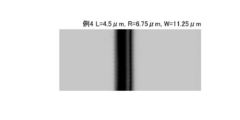
- FIGS. 33 and 34 show simulation results in the case where the slit width W is 11.25 ⁇ m by setting L to 4.5 ⁇ m and R to 6.75 ⁇ m.
- Example 3 to Example 4 only R is changed with L being constant.
- the number of lines of electric force lines toward the counter substrate 6 increases, and the amount of liquid crystal molecules aligned in the opposite direction decreases.
- the portion where the liquid crystal molecules continuously rotate from the reverse orientation to the normal orientation is reduced, and the dark line generated at the position slightly entering the right side from the end of the right pixel electrode 8 is on the left side, that is, the end of the pixel electrode 8. Shifting closer.
- the right-side pixel since the direction of the lines of electric force has changed upward, the right-side pixel has a stronger regulation force on the orientation, and the right-side pixel also has increased transmittance.
- FIGS. 35 and 36 show simulation results when the slit width W is 12.25 ⁇ m by setting L to 4.5 ⁇ m and R to 7.75 ⁇ m. This is a value obtained by further increasing R by 1 ⁇ m from Example 4.
- the lines of electric lines of force are generated inside the right pixel, the influence of the regulating force of the electric lines of force is exerted on the part away from the left end of the right pixel electrode 8 toward the right.
- the orientation direction of molecules is shifted.
- the transmittance curve inside the right pixel becomes gentle, causing a decrease in transmittance.
- Example 1 When the transmittance curves in the comparative example and the examples 2 to 5 are superimposed and displayed, the result is as shown in FIG. In FIG. 37, Example 1 is not displayed because the degree of the effect is small.
- Example 1 In the comparative example, there are a total of two dark lines, a dark line that overlaps the middle line 16 of the gap 14 between the pixel electrodes 8 and a dark line at a position separated from the inside of the pixel in the vicinity thereof, and between the two dark lines.
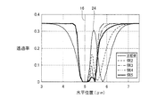
- a transmittance peak 24 occurs. From Example 2 to Example 5, as the slit width W gradually increases, the height of the peak 24 decreases, and the edge of the saturation region of the transmittance in the right pixel shifts toward the left end of the pixel electrode. You can see that This is presumably because the degree of orientation in the opposite direction at the end of the pixel electrode 8 is suppressed by providing the counter electrode 9 with the slit 22.
- Example 5 the height of the transmittance peak 24 is minimum, and the two dark lines are close to each other and are almost indistinguishable. As a result, they appear to be one dark line. In Example 5, the height of the peak 24 is the minimum, but the shoulder of the saturation region of the transmittance in the right pixel is gentle compared to Example 4. Therefore, with respect to the overall transmittance Example 5 is reduced as compared with Example 4.
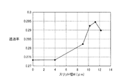
- FIG. 38 shows a graph of the change in overall transmittance when the slit width W is changed in Examples 1 to 5.
- the slit width W is 0, and is included in this graph.
- the transmittance is maximum when the fourth example, that is, the slit width W is 11.25 ⁇ m. Therefore, as a result of this experiment, it has been found that the effect of the present invention is maximized when the slit width W is 11.25 ⁇ m.
- the slit of the counter electrode is centered rather than having the center line coincident with the center line of the gap between the pixel electrodes. It can be said that it is preferable to dispose the lines.
- the side to be shifted is the side where dark lines occur when no slit is provided. In other words, it is as follows.
- the liquid crystal display device according to the present embodiment is the first from the middle line when the slit is not provided in the counter electrode among the middle lines defined as the line passing through the center of the gap between the pixel electrodes.
- the slit is on the first side from the center line.
- the protruding portion is disposed so as to cover the intermediate line so that the protruding width is larger than the protruding width on the second side opposite to the first side.
- the “band-like dark line” means that even though it is strictly a dark line divided into a plurality of lines as in the example shown in FIG. It may be regarded as a dark line of a book. In the example of FIG. 26, the “first side” is the right side, and the “second side” is the left side.
- the slit of the counter electrode is preferably provided so as to be shifted to one side in this way.
- the width of the slit provided in the counter electrode is preferably larger than the width of the gap between the pixel electrodes. This is because, by adopting this configuration, it is possible to sufficiently cope with dark lines generated with a width wider than the width of the gap between the pixel electrodes.
- the slits 22 of the counter electrode 9 do not need to be provided over the entire region serving as the boundary between the adjacent pixels 3 but may be provided at least in part.
- a configuration for electrically connecting them is necessary. Therefore, the slits 22 are intermittently disconnected to the extent that the counter electrode 9 is not completely divided. Is preferably provided. If shown in plan view, for example, the ones shown in FIGS. 39 and 40 can be considered.
- one slit 22 is provided for each domain side.
- one slit 22 is provided for each side of the pixel. Two domains edges along one side of the pixel is located. In each of these two domain sides, the center line of the slit 22 is at a different position, so that the slit 22 has a shape in which the center line is shifted in the middle.
- the alignment film has been described as having a specific alignment azimuth set by exposure, but the method for setting the alignment azimuth in the alignment film may be any method other than exposure.
- the present invention can be used for a liquid crystal display device.
- liquid crystal display device 1 liquid crystal display device, 2 display area, 3 pixels, 4 liquid crystal layer, 5 TFT substrate, 6 counter substrate, 7a, 7b polarizing plate, 8 pixel electrode, 9 counter electrode, 11 first alignment film, 12 second alignment film, 13 domains, 14 gaps, 15 regions, 16 midlines, 17 curves (showing transmittance), 18 (correctly oriented) liquid crystal molecules, 19 (tilted in almost opposite orientation) liquid crystal molecules, 20, 21 dark lines, 22 ( Slit, 23 planar area, 24 peaks provided on the counter electrode.
Landscapes
- Physics & Mathematics (AREA)
- Nonlinear Science (AREA)
- Mathematical Physics (AREA)
- Chemical & Material Sciences (AREA)
- Crystallography & Structural Chemistry (AREA)
- General Physics & Mathematics (AREA)
- Optics & Photonics (AREA)
- Spectroscopy & Molecular Physics (AREA)
- Geometry (AREA)
- Liquid Crystal (AREA)
Abstract
液晶表示装置は、表示領域(2)に延在する液晶層(4)と、これを挟み込むように互いに貼り合わせられたTFT基板(5)および対向基板(6)とを備える。TFT基板(5)には、複数の画素(3)の各々に対応して画素電極(8)が設けられている。対向基板(6)には、画素電極(8)と対向するように対向電極(9)が設けられている。画素電極(8)の液晶層(4)側の表面には第1配向膜(11)が配置され、対向電極(9)の液晶層(4)側の表面には第2配向膜(12)が配置されている。画素(3)は、第1および第2配向膜(11,12)の配向方位の組合せがそれぞれ異なった状態となっている複数のドメインを含み、互いに隣接し合う画素(3)同士の境界に対応する領域の少なくとも一部において、対向電極(9)にスリット(22)が設けられている。
Description
本発明は、液晶表示装置に関するものである。特に、1つの画素内に複数のドメインが形成された液晶表示装置に関する。
従来から各種の液晶表示装置が提案されており、特に近年は、視野角の拡大、ディスクリネーションの抑制、焼きつきの低減などを図った各種の液晶表示装置が提案されている。視野角の拡大のためには、1つの画素内に複数のドメインを形成するMVA(Multidomain Vertical Alignment)方式が提案されている。
たとえば、特開2007-249243号公報(特許文献1)には、MVA方式の液晶表示装置の一例が記載されている。特許文献1に記載されたMVA方式の液晶表示装置は、一対の基板と、1つの画素内に形成された複数のドメインと、各ドメインにおける液晶分子の傾く方向を規制するドメイン規制手段とを備える。特許文献1では、ドメイン規制手段として、基板の表面に形成された突起や窪みと、基板に設けられたフィッシュボーン形状の電極とが挙げられている。
このようなドメイン規制手段を設けることで、電圧印加時における各ドメインでの液晶分子の傾斜方向を各々異ならせている。このように、各ドメインにおける液晶分子の傾斜方向を異ならせることで、視野角の向上が図られている。
特開2008-197691号公報(特許文献2)に記載された液晶表示装置は、1つの画素内に形成されたドメインと、液晶層に接する部分に設けられた垂直配向膜とを備えている。垂直配向膜には、斜め方向から紫外線(UV:Ultra Violet光)を照射することによって配向処理が施されている。紫外線の照射方向を位置によって異ならせることで複数のドメインを形成している。この液晶表示装置は、電圧印加時に、各ドメインの配向規制方位に向けて液晶分子が配向するように突起状の構造物を備える。
電圧印加時に液晶分子が配向する方位が異なったものとなる複数のドメインを備えた液晶表示装置においては、画素同士の境界のうち一部の区間の近傍に暗線が生じる。
そこで、本発明は、複数のドメインを備えた液晶表示装置であって、画素同士の境界のうち一部の区間の近傍に生じる暗線の幅を小さく抑えた液晶表示装置を提供することを目的とする。
上記目的を達成するため、本発明に基づく液晶表示装置は、複数の画素を含む表示領域を有し、少なくとも上記表示領域に延在する液晶層と、上記液晶層を挟み込むように互いに貼り合わせられた第1および第2の基板と、上記第1,第2の基板を挟み込むように配置された一対の偏光板とを備える液晶表示装置である。上記第1の基板には、上記複数の画素の各々に対応して画素電極が設けられている。上記第2の基板には、上記画素電極と対向するように対向電極が設けられている。上記画素電極の上記液晶層側の表面には第1配向膜が配置されている。上記対向電極の上記液晶層側の表面には第2配向膜が配置されている。上記画素は、上記第1および第2配向膜の配向方位の組合せがそれぞれ異なった状態となっている複数のドメインを含む。上記複数の画素のうち互いに隣接し合う画素同士の境界に対応する領域の少なくとも一部において、上記対向電極にスリットが設けられている。
本発明によれば、対向電極にスリットが設けられていることにより、画素同士の境界のうち一部の区間の近傍に生じる暗線の幅を小さく抑えることができる。
上述のような暗線が生じる理由について、まず説明する。
複数のドメインを有する液晶表示装置においては、各ドメインごとに液晶分子の姿勢が定まる。液晶層を挟む基板はTFT(Thin Film Transistor)基板と対向基板と呼ぶものとする。対向基板はカラーフィルタを備えるものであってもよい。TFT基板の液晶層側の表面には、図1に示す形状の画素電極が設けられているものとする。TFT基板と対向基板とはいずれも液晶層に接する側の面に配向膜を有する。TFT基板においては、画素電極は配向膜によって覆われている。各ドメインに注目した場合、TFT基板と対向基板とのそれぞれの表面において配向膜が設けられており、これらの配向膜には異なる配向方位が設定されている。各ドメインの内部にある液晶分子のうちTFT基板と対向基板との各配向膜の近傍にあるものは、当該配向膜が有する配向方位に従って傾く。
複数のドメインを有する液晶表示装置においては、各ドメインごとに液晶分子の姿勢が定まる。液晶層を挟む基板はTFT(Thin Film Transistor)基板と対向基板と呼ぶものとする。対向基板はカラーフィルタを備えるものであってもよい。TFT基板の液晶層側の表面には、図1に示す形状の画素電極が設けられているものとする。TFT基板と対向基板とはいずれも液晶層に接する側の面に配向膜を有する。TFT基板においては、画素電極は配向膜によって覆われている。各ドメインに注目した場合、TFT基板と対向基板とのそれぞれの表面において配向膜が設けられており、これらの配向膜には異なる配向方位が設定されている。各ドメインの内部にある液晶分子のうちTFT基板と対向基板との各配向膜の近傍にあるものは、当該配向膜が有する配向方位に従って傾く。
なお、液晶分子の長手方向が基板面となす角度は「チルト角」と呼ぶものとする。基板に垂直な方向から見たときの液晶分子が傾いている方位を「チルト方位」と呼ぶものとする。画素電極に電圧を印加しない状態でのチルト角、チルト方位をそれぞれプレチルト角、プレチルト方位と呼ぶものとする。
液晶層の厚み方向に沿って配向膜からの距離が遠くなるにつれて液晶分子の姿勢が配向膜の影響を受ける度合いは減る。特にTFT基板の配向膜が有する配向方位と対向基板の配向膜が有する配向方位が異なる場合は、液晶分子のチルト方位は厚み方向に沿って変化することとなる。液晶層の厚み方向の中央においては、液晶分子は、TFT基板の配向膜によって定まるチルト方位と対向基板の配向膜によって定まるチルト方位との平均に相当するチルト方位に傾く。
一方、画素の外形線の近傍においては画素電極の端が生じさせる斜め電界の影響により、液晶分子は画素の外形線に対して垂直かつ外形線の内側向きの方位に傾こうとする。
各画素内における液晶分子のチルト方位の定まり方の一例について、より詳しく説明する。各画素においては、図1に示す形状の画素電極がTFT基板側に設けられているものとする。実際には基板上には多数の画素が配列されているが、以下、1つの画素内での様子に注目して説明する。この例では、TFT基板上では、図2に示すように、各画素が左右に2つの領域に分割され、各領域ごとに設定された方向で配向膜の露光が行なわれるものとする。対向基板上では、図3に示すように各画素が上下に2つの領域に分割され、各領域ごとに設定された方向で配向膜の露光が行なわれるものとする。図2、図3における矢印は露光時の光の照射方向を示す。
以下、液晶分子の傾きを記号化して示す。たとえば基板上面において図4に矢印で示すように左向きに配向方位が設定され、かつ、液晶分子が傾いている場合、この液晶分子を基板の上方から見たものと仮定すれば図4における液晶分子の左端が観察者にとっては近くに見えるので、その端を楕円形の頭で表示する。図4における液晶分子の右端は観察者にとって遠くに見えるので、尖った尻尾で表示する。その結果、図4に対応する液晶分子の様子は図5のようにオタマジャクシ(tadpole)形状で表示される。液晶分子のチルト方位はオタマジャクシ形状の頭の向きによって把握することができる。
配向膜に対して一定の傾いた方向から露光することによって配向膜は一定の配向方位を獲得する。配向方位は露光方向と逆向きとなる。図2に示すようにTFT基板に露光した結果、TFT基板の表面の配向膜においては、図6に示すような配向方位となる。図3に示すように対向基板に露光した結果、対向基板の表面の配向膜においては、図7に示すような配向方位となる。図6、図7における矢印は設定された配向方位を意味し、配向膜が配向膜近傍の液晶分子を当該方位に傾かせる性質を有することを意味する。
図6に示したTFT基板に対して、図7に示した対向基板を左右反転させるように裏返して上側から被せ、TFT基板と対向基板との間に液晶層を保持したものと想定する。こうして、図8に示すように1つの画素内に4つのドメインが形成される。図8において上下方向の矢印として表示されている矢印はTFT基板の上面に形成された配向膜が有する配向方位である。図8において左右方向の矢印として表示されている矢印は対向基板の下面に形成された配向膜が有する配向方位である。対向基板の下面の配向膜によって傾く液晶分子は図9に示すように、観察者からは対向基板を透過するようにして観察されることとなる。液晶分子の対向基板側の端が観察者から近い端となるので、この端がオタマジャクシ形状の頭として表示される。
図8においては、各ドメインの内部に液晶分子を示すオタマジャクシ形状が2つずつ重なって表示されているが、紙面手前側のオタマジャクシ形状が対向基板の近傍の液晶分子のチルト方位を表す。紙面奥側のオタマジャクシ形状がTFT基板の近傍の液晶分子のチルト方位を表す。各ドメイン内においては、TFT基板の近傍の液晶分子に現れるチルト方位と対向基板の近傍の液晶分子に現れるチルト方位とは90°をなして交差している。
液晶層の厚み方向の中央においては、図8に表示された2つのチルト方位を合成した向きに液晶分子が傾くこととなるので、各ドメイン内における厚み方向の中央での液晶分子のチルト方位は図10に示すようになる。電圧を印加したときには、TFT基板に設けられた画素電極の外形線近傍においては斜め電界が発生し、図11に示すようになる。すなわち、画素電極の外形線近傍にある液晶分子は斜め電界の影響により外形線に垂直な側に傾こうとする。図11では画素電極の外形線上に液晶分子の傾きを表示している。
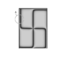
図11に示される各ドメインの外形線のうち画素の外形線と兼ねる辺を「ドメイン辺」と呼ぶものとする。1つの画素の中には8本のドメイン辺を想定することができる。画素の1つの辺はそれぞれ2つのドメイン辺からなる。液晶分子の記号の頭同士が向き合っているドメイン辺においては、液晶分子の向きが乱れ、暗線となる。また、ドメイン同士が隣接する箇所においても、液晶分子のチルト角は90°異なることとなるので暗線が生じる。結果的に、図12に示すようにドメイン同士の境界と、画素の外形線上の4つのドメイン辺とにおいて暗線が生じる。1つの画素の全体としては鉤十字(swastika)の形状に暗線が現れる。暗線の発生状況を確認するために行なった透過状態のシミュレーション結果を図13に示す。
液晶分子を示す記号と暗線発生のシミュレーション結果とを重ねたところを図14に示す。図14において破線の楕円で囲まれた区間において暗線が生じている。
発明者らが液晶層4における液晶分子の挙動をシミュレーションによって検討したところを図15に示す。TFT基板5の上面に画素電極8が形成されており、対向基板6の下面に対向電極9が形成されている。TFT基板5と対向基板6とは液晶層4を挟み込むように対向して配置されている。図15では、画素電極8間の間隙14の近傍を表示している。液晶層4の中に表示された多数のピン状の図形は、各部位における液晶分子の姿勢を示している。ただし、液晶分子が傾く方位をわかりやすくするために傾きは誇張して表示されている場合がある。液晶層4に表示された曲線17は液晶層4の当該部位における透過率をグラフ化して示すものである。図15によれば、間隙14において透過率が低下している他に、間隙14から少し離れたところの領域15においても透過率が局所的に低下していることがわかる。この領域15が図13のA部で太い暗線として見えている部分に対応する。図15のシミュレーション結果を簡略化したものを図16に示す。画素電極8の内部のうち画素電極8の端から離れた場所では、液晶分子18は正しい方位(以下「正方位」という。)に傾いている。正方位とは図10にオタマジャクシ形状で示したように、平面的に見て画素電極8の外辺に対して45°をなす方位である。図15、図16に示すように、画素電極8間の間隙14においては電気力線が間隙14を通り抜けるように集中しているので、間隙14の投影領域内における液晶分子はいずれもその影響を受けている。たとえば液晶分子19は正方位とはほぼ逆の方位(以下「逆方位」という。)に傾いている。暗線となる領域15においては、液晶分子の方位は、狭い区間の中で逆方位から正方位へと急激に変化している。このように液晶分子の方位が急激に変化していることが暗線の原因となっていると考えられる。この部位における透過状態のシミュレーション結果を図17に示す。画素電極8同士の間の間隙の中心線が中線16である。中線16に沿って暗線20が生じており、暗線20の右側にもう1本の暗線21が生じている。図17における暗線21が図15、図16における領域15に相当する。図17においては、暗線20と暗線21とを併せて1本の帯状の暗線とみなすこともできる。
発明者らは、上述のような原理で暗線が生じていることに着目し、そのような暗線の発生を抑制するために本発明をなしとげた。
(実施の形態1)
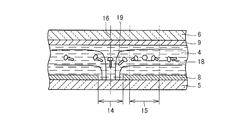
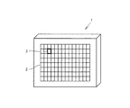
図18~図20を参照して、本発明に基づく実施の形態1における液晶表示装置について説明する。図18に示すように、本実施の形態における液晶表示装置1は、複数の画素3を含む表示領域2を有する。図19に示すように、液晶表示装置1は、少なくとも表示領域2に延在する液晶層4と、液晶層4を挟み込むように互いに貼り合わせられた第1および第2の基板としてのTFT基板5および対向基板6と、前記第1,第2の基板を挟み込むように配置された一対の偏光板7a,7bとを備える。前記第1の基板としてのTFT基板5には、複数の画素3の各々に対応して画素電極8が設けられている。前記第2の基板としての対向基板6には、画素電極8と対向するように対向電極9が設けられている。画素電極8の液晶層4側の表面には第1配向膜11が配置されている。対向電極9の液晶層4側の表面には第2配向膜12が配置されている。図19では、説明の便宜のため、TFT、配線、コンタクトホールなどの構造物を図示省略している。図20に示すように、画素3は、前記第1および第2配向膜の配向方位の組合せがそれぞれ異なった状態となっている複数のドメイン13を含む。図19に示すように、複数の画素3のうち互いに隣接し合う画素3同士の境界に対応する領域の少なくとも一部において、対向電極9にスリット22が設けられている。
図18~図20を参照して、本発明に基づく実施の形態1における液晶表示装置について説明する。図18に示すように、本実施の形態における液晶表示装置1は、複数の画素3を含む表示領域2を有する。図19に示すように、液晶表示装置1は、少なくとも表示領域2に延在する液晶層4と、液晶層4を挟み込むように互いに貼り合わせられた第1および第2の基板としてのTFT基板5および対向基板6と、前記第1,第2の基板を挟み込むように配置された一対の偏光板7a,7bとを備える。前記第1の基板としてのTFT基板5には、複数の画素3の各々に対応して画素電極8が設けられている。前記第2の基板としての対向基板6には、画素電極8と対向するように対向電極9が設けられている。画素電極8の液晶層4側の表面には第1配向膜11が配置されている。対向電極9の液晶層4側の表面には第2配向膜12が配置されている。図19では、説明の便宜のため、TFT、配線、コンタクトホールなどの構造物を図示省略している。図20に示すように、画素3は、前記第1および第2配向膜の配向方位の組合せがそれぞれ異なった状態となっている複数のドメイン13を含む。図19に示すように、複数の画素3のうち互いに隣接し合う画素3同士の境界に対応する領域の少なくとも一部において、対向電極9にスリット22が設けられている。
本実施の形態では、図20に例示するように、1つの画素3は4つのドメイン13を含む。画素電極8および対向電極9はITO(Indium Tin Oxide)によって形成されたものであってよい。
対向基板6は、カラーフィルタが形成された基板であってもよい。
本実施の形態では、上述のように対向電極9にスリット22が設けられていることにより、画素同士の境界のうち一部の区間の近傍に生じる暗線の幅を小さく抑えることができる。その効果を確認するために、発明者らは、シミュレーションを行なった。その結果を図21に示す。図21のシミュレーション結果を簡素化したものを図22に示す。本実施の形態における液晶表示装置で得られる暗線の状況を図23に示す。
本実施の形態では、上述のように対向電極9にスリット22が設けられていることにより、画素同士の境界のうち一部の区間の近傍に生じる暗線の幅を小さく抑えることができる。その効果を確認するために、発明者らは、シミュレーションを行なった。その結果を図21に示す。図21のシミュレーション結果を簡素化したものを図22に示す。本実施の形態における液晶表示装置で得られる暗線の状況を図23に示す。
本実施の形態では、対向電極9にスリット22が設けられていることにより、電気力線の一部は、対向基板9側のスリット22に抜けることとなる。液晶分子は電気力線に沿って傾くので、液晶分子のいわゆる配向ロスが減少する。結果的に、図23に示すように暗線は1本にまとまり、画素同士の境界の近傍に生じる暗線の合計幅は小さくなる。図23では暗線が完全に消滅したわけではないが、図17に示した暗線に比べれば明らかに幅が小さくなっている。これにより、暗線の幅を小さく抑えるという効果を得ることができているといえる。
対向電極9におけるスリット22は、画素電極8の間隙14の幅と一致しているとは限らない。図22に示したように、スリット22は、間隙14よりも幅が広いものとなっていてもよい。スリット22の中心線は、間隙14の中線16と一致しているとは限らない。スリット22は、一方の画素の側に偏って配置されていてよい。図17に示したように、元々、右側の画素に入り込んだ位置において暗線が生じていたが、本実施の形態では、図22に示すように、スリット22は、元々暗線が生じていた側の画素に偏るように配置されている。
このように暗線が元々生じていた側にスリットが入り込む量を調整することにより、液晶分子が逆方位になる度合いを抑制することができる。その結果、暗線の生じる場所を画素電極8間の間隙14の側へ追いやることができ、生じる暗線の幅自体も小さくすることができる。元々、図17に示すように暗線が中線16より左側にはみ出す幅は、暗線が中線16より右側にはみ出す幅に比べて少ない。本実施の形態で示すように、対向電極9にスリット22を設けたことにより、左側の画素における電気力線の分布が規制され、その結果、透過率の曲線は図21に示すように急峻となる。図21と図15とを比較すれば、左側の画素における透過率の曲線が変化していることがわかる。図23と図17とを対比すれば、図17では暗線の幅方向の両端がぼんやりしていたのに対して、図23では暗線の幅方向の両端の外形線が比較的はっきりしていることがわかる。
なお、スリット22は、互いに隣接し合う画素同士の境界線のうち対向電極9にスリットを設けなかった場合に暗線が生じる区間に設けられていることが好ましい。このような構成とすることにより、生じる暗線の幅の削減効果が特に大きくなるからである。
より正確にいえば、スリット22は、複数のドメイン13の各々の外側の辺であってなおかつ複数の画素3の各々の外側の辺でもある辺すなわちドメイン辺のうち、画素電極8と対向電極9との間に電圧が印加されることによって前記複数のドメイン13の各々の中央部において液晶層4の液晶分子が傾けられたときの前記液晶分子の長手方向の対向電極9側の端が向く側の辺に設けられていることが好ましい。なぜなら、原理からすれば、このような辺に暗線が太く生じるものであり、このような辺にスリットを設けることによって、生じる暗線の幅の削減効果が特に大きくなるからである。
(透過状態のシミュレーションの条件)
なお、図13に示した透過状態のシミュレーションに当たっては、1つの画素に相当する領域として、図24に示すように、縦230.75μm、横153.75μmの長方形の平面領域23を想定し、この平面領域23の内側において、上下左右に3μmの間隙をあけて画素電極8が配置されているものとした。したがって、画素電極8同士の間の間隙14の幅は6μmとなる。各基板の配向膜における配向方位は、2枚の基板を重ねた状態で図10に矢印で示す向きとした。すなわち、対向基板では配向膜が上下2つの領域に分割されており、TFT基板では配向膜が左右2つの領域に分割されており、これらが重ね合わされることにより、図10に示したように4つのドメインが形成されている。したがって、各ドメイン内における厚み方向の中央での液晶分子のチルト方位は図10に4つのオタマジャクシ形状でそれぞれ示すようになる。このシミュレーションにおいては、TFT基板5、対向基板6のいずれにおいても液晶分子のプレチルト角は88.2°とした。
なお、図13に示した透過状態のシミュレーションに当たっては、1つの画素に相当する領域として、図24に示すように、縦230.75μm、横153.75μmの長方形の平面領域23を想定し、この平面領域23の内側において、上下左右に3μmの間隙をあけて画素電極8が配置されているものとした。したがって、画素電極8同士の間の間隙14の幅は6μmとなる。各基板の配向膜における配向方位は、2枚の基板を重ねた状態で図10に矢印で示す向きとした。すなわち、対向基板では配向膜が上下2つの領域に分割されており、TFT基板では配向膜が左右2つの領域に分割されており、これらが重ね合わされることにより、図10に示したように4つのドメインが形成されている。したがって、各ドメイン内における厚み方向の中央での液晶分子のチルト方位は図10に4つのオタマジャクシ形状でそれぞれ示すようになる。このシミュレーションにおいては、TFT基板5、対向基板6のいずれにおいても液晶分子のプレチルト角は88.2°とした。
(液晶分子の挙動のシミュレーションの条件)
図24に示した画素を左右に2つ並べたものを図25に示す。図15、図21に示した液晶分子の挙動のシミュレーションに関しては、図25に示すB部を拡大したところとして、図26に示す構造を想定した。このシミュレーションにおいては、現在量産されている液晶表示パネルに多く用いられている方式であるところのドット反転駆動方式を想定し、隣り合う画素電極8a,8b同士の間には互いに逆の電位を印加するものとした。図26に示す「-」、「+」の記号は、画素電極8a,8bにそれぞれ印加される電位を意味する。
図24に示した画素を左右に2つ並べたものを図25に示す。図15、図21に示した液晶分子の挙動のシミュレーションに関しては、図25に示すB部を拡大したところとして、図26に示す構造を想定した。このシミュレーションにおいては、現在量産されている液晶表示パネルに多く用いられている方式であるところのドット反転駆動方式を想定し、隣り合う画素電極8a,8b同士の間には互いに逆の電位を印加するものとした。図26に示す「-」、「+」の記号は、画素電極8a,8bにそれぞれ印加される電位を意味する。
(実験)
対向電極9のスリット22と間隙14の中線16との位置関係を幾通りか変化させて実施した。図26に示すように、スリット22は、中線16に関して非対称に配置されているものとし、スリット22の幅のうち中線16より左にある部分の幅をLとし、中線16より右にある部分の幅をRとした。スリット22全体の幅をWとする。したがって、L+R=Wが常に成り立つ。L,R,Wの長さを幾通りか変化させ、間隙14の幅は一定とした。
対向電極9のスリット22と間隙14の中線16との位置関係を幾通りか変化させて実施した。図26に示すように、スリット22は、中線16に関して非対称に配置されているものとし、スリット22の幅のうち中線16より左にある部分の幅をLとし、中線16より右にある部分の幅をRとした。スリット22全体の幅をWとする。したがって、L+R=Wが常に成り立つ。L,R,Wの長さを幾通りか変化させ、間隙14の幅は一定とした。
図15、図17は、本発明を実施しない場合のシミュレーション結果に相当するので、以下「比較例」という。以下に述べる各例の効果の程度を把握するためには、液晶分子の挙動のシミュレーション結果は、図15と比較すべきであり、透過状態のシミュレーションの結果は図17と比較すべきである。
(例1)
まず、本発明に基づく例1として、L,Rとも1.98μmとすることによってスリット幅Wを3.96μmとした場合のシミュレーション結果を図27、図28に示す。例1では、比較例に比べればわずかに改善されているが、対向電極9のスリット22による電界への影響が少なく、液晶分子の挙動も、透過状態も比較例に比べてごく微小な改善しか見られなかった。
まず、本発明に基づく例1として、L,Rとも1.98μmとすることによってスリット幅Wを3.96μmとした場合のシミュレーション結果を図27、図28に示す。例1では、比較例に比べればわずかに改善されているが、対向電極9のスリット22による電界への影響が少なく、液晶分子の挙動も、透過状態も比較例に比べてごく微小な改善しか見られなかった。
(例2)
本発明に基づく例2として、L,Rとも4.5μmとすることによってスリット幅Wを9.0μmとした場合のシミュレーション結果を図29、図30に示す。例2では、対向電極9のスリット22の影響で電気力線が変化し、液晶分子の配向が変化している。左側の画素電極8の端部での電気力線が上向きに変化したことにより、左側の画素電極8における配向への規制力が強くなり、比較例ではなだらかに変化していた液晶分子の姿勢が急激に変化している。この結果、比較例に比べて左側の画素電極8の端部付近の透過率が大幅に上がっている。
本発明に基づく例2として、L,Rとも4.5μmとすることによってスリット幅Wを9.0μmとした場合のシミュレーション結果を図29、図30に示す。例2では、対向電極9のスリット22の影響で電気力線が変化し、液晶分子の配向が変化している。左側の画素電極8の端部での電気力線が上向きに変化したことにより、左側の画素電極8における配向への規制力が強くなり、比較例ではなだらかに変化していた液晶分子の姿勢が急激に変化している。この結果、比較例に比べて左側の画素電極8の端部付近の透過率が大幅に上がっている。
(例3)
本発明に基づく例3として、Lを4.5μmとし、Rを5.75μmとすることによってスリット幅Wを10.25μmとした場合のシミュレーション結果を図31、図32に示す。
本発明に基づく例3として、Lを4.5μmとし、Rを5.75μmとすることによってスリット幅Wを10.25μmとした場合のシミュレーション結果を図31、図32に示す。
(例4)
本発明に基づく例4として、Lを4.5μmとし、Rを6.75μmとすることによってスリット幅Wを11.25μmとした場合のシミュレーション結果を図33、図34に示す。
本発明に基づく例4として、Lを4.5μmとし、Rを6.75μmとすることによってスリット幅Wを11.25μmとした場合のシミュレーション結果を図33、図34に示す。
例3~例4では、Lを一定としてRのみを変化させたことになる。図31、図33を参照すれば、Rを大きくするにつれて、対向基板6側への電気力線の抜けが多くなり、逆方位に配向する液晶分子の量が減少している。その結果、液晶分子が逆方位から正方位へと連続的に回転する部分が減り、右側の画素電極8の端から少し右側に入り込んだ位置で生じていた暗線が左側すなわち画素電極8の端に近い側へとシフトしている。また、電気力線の向きが上向きに変化したことにより、右側の画素においても配向への規制力が強くなり、右側の画素においても、透過率が上昇している。
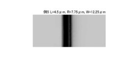
(例5)
例5として、Lを4.5μmとし、Rを7.75μmとすることによってスリット幅Wを12.25μmとした場合のシミュレーション結果を図35、図36に示す。これは、例4よりRをさらに1μm大きくしたものである。この場合、電気力線の切れ目が右側の画素の内部に生じるので、右側の画素電極8の左端から右に向かって離れた部位に電気力線の規制力の影響が出ている、すなわち、液晶分子の配向方位がずれている。これに伴い、右側の画素の内部での透過率曲線はなだらかになり、透過率の低下を引き起こしている。
例5として、Lを4.5μmとし、Rを7.75μmとすることによってスリット幅Wを12.25μmとした場合のシミュレーション結果を図35、図36に示す。これは、例4よりRをさらに1μm大きくしたものである。この場合、電気力線の切れ目が右側の画素の内部に生じるので、右側の画素電極8の左端から右に向かって離れた部位に電気力線の規制力の影響が出ている、すなわち、液晶分子の配向方位がずれている。これに伴い、右側の画素の内部での透過率曲線はなだらかになり、透過率の低下を引き起こしている。
比較例および例2~5における透過率曲線を重ね合わせて表示すると図37に示すようになる。図37では、例1は効果の程度が小さいので表示していない。比較例では、画素電極8同士の間隙14の中線16に重なる暗線と、その近傍において画素の内側に離隔した位置の暗線との合計2本の暗線が生じ、その2本の暗線の間に透過率のピーク24が生じている。例2から例5へと、スリット幅Wが徐々に大きくなるにつれて、このピーク24の高さが低くなり、かつ、右側の画素における透過率の飽和領域のエッジが画素電極の左端に向かってシフトしていることがわかる。これは対向電極9にスリット22を設けたことにより、画素電極8の端における逆方位への配向度合いが抑制されるからであると考えられる。
例5においては、透過率のピーク24の高さが最小となり、2本の暗線は互いに接近して区別がほぼなくなり、その結果、1本の暗線のように見える状態となっている。例5においては、ピーク24の高さは最小となっているが、右側の画素における透過率の飽和領域の肩が例4に比べてなだらかとなっている。そのため、全体的な透過率に関しては例5は例4に比べて低下している。
例1~例5にわたってスリット幅Wを変化させた際の全体的な透過率の変化をグラフにしたものを図38に示す。比較例はスリット幅Wが0であるものとみなして、このグラフに盛り込んで表示している。図38によれば、例4すなわちスリット幅Wが11.25μmのときに透過率が最大となっている。したがって、この実験の結果としては、スリット幅Wが11.25μmのときに本発明の効果が最大となることがわかった。
この最適値は、他のパラメータが変化した場合に変化し得るが、本発明としては、対向電極のスリットは、画素電極同士の間の間隙の中線に中心線を一致させて設けるよりも中心線をずらして設けた方が好ましいといえる。ただし、そのずらすべき側は、スリットを設けなかった場合に暗線が生じる側である。これを言い換えれば、以下のようになる。本実施の形態における液晶表示装置としては、前記画素電極同士の間の間隙の中心を通る線として規定される中線のうち前記対向電極に前記スリットを設けなかった場合に前記中線から第1の側にずれた前記中線と平行な線を中心線として前記中線と平行かつ前記中線に重なるように帯状の暗線が生じる区間において、前記スリットは、前記中線より前記第1の側にはみ出す幅が前記中線の前記第1の側とは反対の第2の側にはみ出す幅より大きくなるように前記中線を覆うように配置されていることが好ましい。ここでいう「帯状の暗線」とは、図17に示した例のように、厳密には複数本に分かれた暗線であっても、これらが互いに近接した位置で生じることにより、全体としてほぼ1本の暗線とみなせるものであってもよい。図26の例でいえば、「第1の側」とは右側であり、「第2の側」とは左側である。対向電極のスリットはこのように一方の側にずらして設けることが好ましい。この構成を採用することにより、スリットに電気力線が抜ける側を暗線発生箇所と大きく重ねることができ、効率良く暗線発生を抑制することができる。
図26に示されるように、対向電極に設けられるスリットの幅は、画素電極同士の間の間隙の幅より大きいことが好ましい。なぜなら、この構成を採用することにより、画素電極同士の間の間隙の幅より広い幅で生じる暗線に対しても十分対応することができるからである。
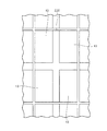
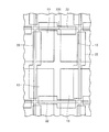
なお、対向電極9のスリット22は、互いに隣接し合う画素3同士の境界となる領域の全てにわたって設けられている必要はなく、少なくとも一部に設けられていればよい。対向電極9がスリット22によって完全に分割されてしまう構造とした場合、それらを電気的に接続するための構成が必要となるので、スリット22は、対向電極9を完全には分割しない程度に断続的に設けられていることが好ましい。平面図で示せば、たとえば図39、図40に示すようなものが考えられる。
図39では、ドメイン辺ごとに1本のスリット22が設けられている。図40では、画素の1本の辺ごとに1本のスリット22が設けられている。画素の1本の辺に沿って2本のドメイン辺が配置されている。これらの2本のドメイン辺の各々においては、スリット22の中心線が異なる位置となっているので、スリット22は、途中で中心線がずれた形状となっている。
なお、上述の説明では、配向膜は露光によって特定の配向方位を設定されるものとして説明したが、配向膜における配向方位の設定方法は露光以外の何らかの方法であってもよい。
なお、今回開示した上記実施の形態はすべての点で例示であって制限的なものではない。本発明の範囲は上記した説明ではなくて請求の範囲によって示され、請求の範囲と均等の意味および範囲内でのすべての変更を含むものである。
本発明は、液晶表示装置に利用することができる。
1 液晶表示装置、2 表示領域、3 画素、4 液晶層、5 TFT基板、6 対向基板、7a,7b 偏光板、8 画素電極、9 対向電極、11 第1配向膜、12 第2配向膜、13 ドメイン、14 間隙、15 領域、16 中線、17 (透過率を示す)曲線、18 (正しい姿勢の)液晶分子、19 (ほぼ逆の方位に傾く)液晶分子、20,21 暗線、22 (対向電極に設けられる)スリット、23 平面領域、24 ピーク。
Claims (5)
- 複数の画素を含む表示領域(2)を有し、
少なくとも前記表示領域に延在する液晶層(4)と、
前記液晶層を挟み込むように互いに貼り合わせられた第1および第2の基板と、
前記第1,第2の基板を挟み込むように配置された一対の偏光板(7a,7b)とを備える液晶表示装置であって、
前記第1の基板には、前記複数の画素の各々に対応して画素電極(8)が設けられ、
前記第2の基板には、前記画素電極と対向するように対向電極(9)が設けられ、
前記画素電極の前記液晶層側の表面には第1配向膜(11)が配置され、
前記対向電極の前記液晶層側の表面には第2配向膜(12)が配置され、
前記画素は、前記第1および第2配向膜の配向方位の組合せがそれぞれ異なった状態となっている複数のドメイン(13)を含み、
前記複数の画素のうち互いに隣接し合う画素同士の境界に対応する領域の少なくとも一部において、前記対向電極にスリット(22)が設けられている、液晶表示装置。 - 前記スリットは、互いに隣接し合う前記画素同士の境界線のうち前記対向電極に前記スリットを設けなかった場合に暗線が生じる区間に設けられている、請求項1に記載の液晶表示装置。
- 前記スリットは、前記複数のドメインの各々の外側の辺であってなおかつ前記複数の画素の各々の外側の辺でもある辺のうち、前記画素電極と前記対向電極との間に電圧が印加されることによって前記複数のドメインの各々の中央部において前記液晶層の液晶分子が傾けられたときの前記液晶分子の長手方向の前記対向電極側の端が向く側の辺に設けられている、請求項1または2に記載の液晶表示装置。
- 前記画素電極同士の間の間隙の中心を通る線として規定される中線(16)のうち前記対向電極に前記スリットを設けなかった場合に前記中線から第1の側にずれた前記中線と平行な線を中心線として前記中線と平行かつ前記中線に重なるように帯状の暗線が生じる区間において、前記スリットは、前記中線より前記第1の側にはみ出す幅が前記中線の前記第1の側とは反対の第2の側にはみ出す幅より大きくなるように前記中線を覆うように配置されている、請求項1から3のいずれかに記載の液晶表示装置。
- 前記スリットの幅は、前記画素電極同士の間の間隙の幅より大きい、請求項1から4のいずれかに記載の液晶表示装置。
Priority Applications (1)
| Application Number | Priority Date | Filing Date | Title |
|---|---|---|---|
| US13/985,026 US20130321747A1 (en) | 2011-02-15 | 2012-02-10 | Liquid crystal display device |
Applications Claiming Priority (2)
| Application Number | Priority Date | Filing Date | Title |
|---|---|---|---|
| JP2011029749 | 2011-02-15 | ||
| JP2011-029749 | 2011-02-15 |
Publications (1)
| Publication Number | Publication Date |
|---|---|
| WO2012111558A1 true WO2012111558A1 (ja) | 2012-08-23 |
Family
ID=46672483
Family Applications (1)
| Application Number | Title | Priority Date | Filing Date |
|---|---|---|---|
| PCT/JP2012/053117 Ceased WO2012111558A1 (ja) | 2011-02-15 | 2012-02-10 | 液晶表示装置 |
Country Status (2)
| Country | Link |
|---|---|
| US (1) | US20130321747A1 (ja) |
| WO (1) | WO2012111558A1 (ja) |
Cited By (1)
| Publication number | Priority date | Publication date | Assignee | Title |
|---|---|---|---|---|
| JP2019515344A (ja) * | 2016-04-28 | 2019-06-06 | 深▲せん▼市華星光電技術有限公司Shenzhen China Star Optoelectronics Technology Co., Ltd. | 液晶パネル及び液晶ディスプレイ |
Families Citing this family (18)
| Publication number | Priority date | Publication date | Assignee | Title |
|---|---|---|---|---|
| NZ773822A (en) | 2015-03-16 | 2022-07-29 | Magic Leap Inc | Methods and systems for diagnosing and treating health ailments |
| IL256276B (en) | 2015-06-15 | 2022-09-01 | Magic Leap Inc | Display system with optical components for coupling multiple light streams |
| EP3440497B1 (en) | 2016-04-08 | 2023-08-16 | Magic Leap, Inc. | Augmented reality systems and methods with variable focus lens elements |
| IL312713A (en) | 2016-11-18 | 2024-07-01 | Magic Leap Inc | Waveguide light multiplexer using crossed gratings |
| US11067860B2 (en) | 2016-11-18 | 2021-07-20 | Magic Leap, Inc. | Liquid crystal diffractive devices with nano-scale pattern and methods of manufacturing the same |
| KR102533671B1 (ko) | 2016-11-18 | 2023-05-16 | 매직 립, 인코포레이티드 | 공간 가변적 액정 회절 격자들 |
| IL304304B2 (en) | 2016-12-08 | 2024-08-01 | Magic Leap Inc | Diffractive devices based on cholesteric liquid crystal |
| KR102550742B1 (ko) | 2016-12-14 | 2023-06-30 | 매직 립, 인코포레이티드 | 표면 정렬 패턴들의 소프트-임프린트 복제를 이용한 액정들의 패터닝 |
| AU2018210527B2 (en) | 2017-01-23 | 2022-12-01 | Magic Leap, Inc. | Eyepiece for virtual, augmented, or mixed reality systems |
| IL307602A (en) | 2017-02-23 | 2023-12-01 | Magic Leap Inc | Variable focus virtual imagers based on polarization conversion |
| IL269317B2 (en) | 2017-03-21 | 2023-11-01 | Magic Leap Inc | An eye imaging device that uses optical refractive elements |
| EP3685215B1 (en) | 2017-09-21 | 2024-01-03 | Magic Leap, Inc. | Augmented reality display with waveguide configured to capture images of eye and/or environment |
| CA3084011C (en) | 2017-12-15 | 2024-06-11 | Magic Leap, Inc. | Eyepieces for augmented reality display system |
| CN109270740A (zh) * | 2018-11-12 | 2019-01-25 | 成都中电熊猫显示科技有限公司 | 液晶显示面板、显示装置及对向基板的制造方法 |
| CN109239970A (zh) * | 2018-11-12 | 2019-01-18 | 成都中电熊猫显示科技有限公司 | 阵列基板、液晶显示面板及显示装置 |
| CN109254453A (zh) * | 2018-11-12 | 2019-01-22 | 成都中电熊猫显示科技有限公司 | 液晶显示面板、显示装置及彩膜基板的制造方法 |
| WO2020106824A1 (en) | 2018-11-20 | 2020-05-28 | Magic Leap, Inc. | Eyepieces for augmented reality display system |
| CN114286962A (zh) | 2019-06-20 | 2022-04-05 | 奇跃公司 | 用于增强现实显示系统的目镜 |
Citations (4)
| Publication number | Priority date | Publication date | Assignee | Title |
|---|---|---|---|---|
| JPH0643461A (ja) * | 1992-04-30 | 1994-02-18 | Internatl Business Mach Corp <Ibm> | 液晶表示装置 |
| JP2004227008A (ja) * | 2004-04-12 | 2004-08-12 | Sanyo Electric Co Ltd | 液晶表示装置 |
| JP2009109767A (ja) * | 2007-10-30 | 2009-05-21 | Sharp Corp | 液晶表示装置 |
| JP2011002648A (ja) * | 2009-06-18 | 2011-01-06 | Toshiba Mobile Display Co Ltd | 液晶表示装置 |
Family Cites Families (10)
| Publication number | Priority date | Publication date | Assignee | Title |
|---|---|---|---|---|
| JPH10186366A (ja) * | 1996-12-26 | 1998-07-14 | Fujitsu Ltd | 液晶表示装置 |
| KR100354904B1 (ko) * | 1998-05-19 | 2002-12-26 | 삼성전자 주식회사 | 광시야각액정표시장치 |
| US6642984B1 (en) * | 1998-12-08 | 2003-11-04 | Fujitsu Display Technologies Corporation | Liquid crystal display apparatus having wide transparent electrode and stripe electrodes |
| US6977704B2 (en) * | 2001-03-30 | 2005-12-20 | Fujitsu Display Technologies Corporation | Liquid crystal display |
| JP4829501B2 (ja) * | 2005-01-06 | 2011-12-07 | シャープ株式会社 | 液晶表示装置 |
| JP4738000B2 (ja) * | 2005-01-19 | 2011-08-03 | シャープ株式会社 | 液晶表示装置 |
| US7679703B2 (en) * | 2005-09-30 | 2010-03-16 | Sharp Kabushiki Kaisha | Liquid crystal display unit |
| CN102298235B (zh) * | 2006-01-26 | 2015-05-27 | 夏普株式会社 | 液晶显示装置的制造方法和液晶显示装置 |
| ATE548676T1 (de) * | 2007-04-20 | 2012-03-15 | Sharp Kk | Flüssigkristallanzeigeanordnungs- herstellungsverfahren und flüssigkristallanzeigeanordnung |
| US8421972B2 (en) * | 2007-12-28 | 2013-04-16 | Sharp Kabushiki Kaisha | Liquid crystal display device |
-
2012
- 2012-02-10 WO PCT/JP2012/053117 patent/WO2012111558A1/ja not_active Ceased
- 2012-02-10 US US13/985,026 patent/US20130321747A1/en not_active Abandoned
Patent Citations (4)
| Publication number | Priority date | Publication date | Assignee | Title |
|---|---|---|---|---|
| JPH0643461A (ja) * | 1992-04-30 | 1994-02-18 | Internatl Business Mach Corp <Ibm> | 液晶表示装置 |
| JP2004227008A (ja) * | 2004-04-12 | 2004-08-12 | Sanyo Electric Co Ltd | 液晶表示装置 |
| JP2009109767A (ja) * | 2007-10-30 | 2009-05-21 | Sharp Corp | 液晶表示装置 |
| JP2011002648A (ja) * | 2009-06-18 | 2011-01-06 | Toshiba Mobile Display Co Ltd | 液晶表示装置 |
Cited By (1)
| Publication number | Priority date | Publication date | Assignee | Title |
|---|---|---|---|---|
| JP2019515344A (ja) * | 2016-04-28 | 2019-06-06 | 深▲せん▼市華星光電技術有限公司Shenzhen China Star Optoelectronics Technology Co., Ltd. | 液晶パネル及び液晶ディスプレイ |
Also Published As
| Publication number | Publication date |
|---|---|
| US20130321747A1 (en) | 2013-12-05 |
Similar Documents
| Publication | Publication Date | Title |
|---|---|---|
| WO2012111558A1 (ja) | 液晶表示装置 | |
| JP5116879B2 (ja) | 液晶表示装置 | |
| JP5555779B2 (ja) | 液晶表示装置 | |
| JP4613973B2 (ja) | 液晶表示素子 | |
| JP5096857B2 (ja) | 液晶表示素子 | |
| WO2011096390A1 (ja) | 液晶表示装置 | |
| WO2013054828A1 (ja) | 液晶表示装置 | |
| CN105793769A (zh) | 液晶显示装置 | |
| CN105974682A (zh) | 液晶显示装置 | |
| CN101241275A (zh) | 液晶显示装置和电子设备 | |
| WO2010097879A1 (ja) | 液晶表示装置 | |
| CN110446971A (zh) | 液晶显示装置 | |
| JP6772001B2 (ja) | 液晶表示装置 | |
| CN105807497B (zh) | 曲面液晶显示器 | |
| JP4902345B2 (ja) | 液晶表示素子 | |
| JP3642634B2 (ja) | 液晶表示パネル及びその製造方法 | |
| CN108780243A (zh) | 液晶显示装置 | |
| JP6042677B2 (ja) | 液晶表示装置 | |
| JP2003280017A (ja) | 液晶表示装置 | |
| JP6607911B2 (ja) | 液晶表示装置 | |
| CN101989011B (zh) | 液晶显示元件 | |
| JP5213482B2 (ja) | 液晶表示素子 | |
| WO2019187158A1 (ja) | 液晶表示パネル | |
| JP2009229970A (ja) | 液晶表示パネル | |
| JP4899872B2 (ja) | 液晶表示装置 |
Legal Events
| Date | Code | Title | Description |
|---|---|---|---|
| 121 | Ep: the epo has been informed by wipo that ep was designated in this application |
Ref document number: 12747389 Country of ref document: EP Kind code of ref document: A1 |
|
| WWE | Wipo information: entry into national phase |
Ref document number: 13985026 Country of ref document: US |
|
| NENP | Non-entry into the national phase |
Ref country code: DE |
|
| 122 | Ep: pct application non-entry in european phase |
Ref document number: 12747389 Country of ref document: EP Kind code of ref document: A1 |
|
| NENP | Non-entry into the national phase |
Ref country code: JP |