WO2012111363A1 - 横型半導体装置 - Google Patents
横型半導体装置 Download PDFInfo
- Publication number
- WO2012111363A1 WO2012111363A1 PCT/JP2012/050425 JP2012050425W WO2012111363A1 WO 2012111363 A1 WO2012111363 A1 WO 2012111363A1 JP 2012050425 W JP2012050425 W JP 2012050425W WO 2012111363 A1 WO2012111363 A1 WO 2012111363A1
- Authority
- WO
- WIPO (PCT)
- Prior art keywords
- insulating film
- gate electrode
- semiconductor device
- semiconductor layer
- electrode
- Prior art date
- Legal status (The legal status is an assumption and is not a legal conclusion. Google has not performed a legal analysis and makes no representation as to the accuracy of the status listed.)
- Ceased
Links
Images



Classifications
-
- H—ELECTRICITY
- H10—SEMICONDUCTOR DEVICES; ELECTRIC SOLID-STATE DEVICES NOT OTHERWISE PROVIDED FOR
- H10D—INORGANIC ELECTRIC SEMICONDUCTOR DEVICES
- H10D30/00—Field-effect transistors [FET]
- H10D30/40—FETs having zero-dimensional [0D], one-dimensional [1D] or two-dimensional [2D] charge carrier gas channels
- H10D30/47—FETs having zero-dimensional [0D], one-dimensional [1D] or two-dimensional [2D] charge carrier gas channels having two-dimensional [2D] charge carrier gas channels, e.g. nanoribbon FETs or high electron mobility transistors [HEMT]
- H10D30/471—High electron mobility transistors [HEMT] or high hole mobility transistors [HHMT]
- H10D30/475—High electron mobility transistors [HEMT] or high hole mobility transistors [HHMT] having wider bandgap layer formed on top of lower bandgap active layer, e.g. undoped barrier HEMTs such as i-AlGaN/GaN HEMTs
- H10D30/4755—High electron mobility transistors [HEMT] or high hole mobility transistors [HHMT] having wider bandgap layer formed on top of lower bandgap active layer, e.g. undoped barrier HEMTs such as i-AlGaN/GaN HEMTs having wide bandgap charge-carrier supplying layers, e.g. modulation doped HEMTs such as n-AlGaAs/GaAs HEMTs
-
- H—ELECTRICITY
- H10—SEMICONDUCTOR DEVICES; ELECTRIC SOLID-STATE DEVICES NOT OTHERWISE PROVIDED FOR
- H10D—INORGANIC ELECTRIC SEMICONDUCTOR DEVICES
- H10D64/00—Electrodes of devices having potential barriers
- H10D64/111—Field plates
-
- H—ELECTRICITY
- H10—SEMICONDUCTOR DEVICES; ELECTRIC SOLID-STATE DEVICES NOT OTHERWISE PROVIDED FOR
- H10D—INORGANIC ELECTRIC SEMICONDUCTOR DEVICES
- H10D64/00—Electrodes of devices having potential barriers
- H10D64/20—Electrodes characterised by their shapes, relative sizes or dispositions
- H10D64/27—Electrodes not carrying the current to be rectified, amplified, oscillated or switched, e.g. gates
- H10D64/311—Gate electrodes for field-effect devices
- H10D64/411—Gate electrodes for field-effect devices for FETs
- H10D64/511—Gate electrodes for field-effect devices for FETs for IGFETs
- H10D64/512—Disposition of the gate electrodes, e.g. buried gates
- H10D64/513—Disposition of the gate electrodes, e.g. buried gates within recesses in the substrate, e.g. trench gates, groove gates or buried gates
-
- H—ELECTRICITY
- H10—SEMICONDUCTOR DEVICES; ELECTRIC SOLID-STATE DEVICES NOT OTHERWISE PROVIDED FOR
- H10D—INORGANIC ELECTRIC SEMICONDUCTOR DEVICES
- H10D62/00—Semiconductor bodies, or regions thereof, of devices having potential barriers
- H10D62/80—Semiconductor bodies, or regions thereof, of devices having potential barriers characterised by the materials
- H10D62/85—Semiconductor bodies, or regions thereof, of devices having potential barriers characterised by the materials being Group III-V materials, e.g. GaAs
- H10D62/8503—Nitride Group III-V materials, e.g. AlN or GaN
Definitions
- the present invention relates to a lateral semiconductor device, and more particularly to a lateral semiconductor device in which a source electrode, a drain electrode, and a gate electrode are formed on a nitride semiconductor layer.
- a source electrode and a drain electrode are formed apart from each other on a nitride semiconductor layer, a gate electrode is formed between the source electrode and the drain electrode, and a first electrode is formed on the nitride semiconductor layer.
- a field effect transistor in which an insulating film and a second insulating film are stacked (see, for example, JP-A-2004-200248 (Patent Document 1)).
- the gate electrode has a field plate structure, and an attempt is made to suppress current collapse by forming the first insulating film with SiN.
- the field effect transistor having the above configuration still has a problem that even if the current collapse phenomenon can be suppressed, a leakage current is generated under a high voltage and a breakdown voltage is lowered.
- an object of the present invention is to provide a lateral semiconductor device capable of suppressing a current collapse phenomenon and suppressing a leakage current and improving a withstand voltage.
- a lateral semiconductor device of the present invention is A nitride semiconductor layer; A source electrode and a drain electrode formed on the nitride semiconductor layer or at least part of the nitride semiconductor layer and spaced apart from each other; A gate electrode formed between the source electrode and the drain electrode; A first current for suppressing current collapse formed on the nitride semiconductor layer and in a region between the drain electrode and the gate electrode at a predetermined interval with respect to the gate electrode.
- An insulating film; At least a second insulating film formed to fill a region between the gate electrode side end of the first insulating film and the gate electrode is provided.
- current collapse is a phenomenon in which the on-resistance of a transistor in a high-voltage operation becomes higher than the on-resistance of the transistor in a low-voltage operation.
- the first insulating film that suppresses current collapse is formed on the nitride semiconductor layer and in a region between the drain electrode and the gate electrode with a predetermined interval with respect to the gate electrode.
- the second insulating film is formed so as to fill at least the region between the gate electrode side of the first insulating film on the nitride semiconductor layer and the gate electrode.
- the first insulating film and the gate electrode are separated from each other, and the second insulating film is interposed between the end of the first insulating film on the gate electrode side and the gate electrode.
- the withstand voltage can be improved by suppressing the leak current flowing through the gate electrode through the first insulating film.
- the source electrode and the drain electrode may be formed on the nitride semiconductor layer with a space therebetween, or at least partially embedded in the nitride semiconductor layer and with a space between each other. May be.
- the second insulating film includes a portion located on at least the end portion on the gate electrode side of the first insulating film
- the gate electrode includes a base portion formed on the nitride semiconductor layer, and a field plate portion formed so as to extend from the upper side of the base portion toward the drain electrode side on the second insulating film.
- the field plate portion by forming the field plate portion so as to extend on the second insulating film from the upper side of the base portion of the gate electrode formed on the nitride semiconductor layer toward the drain electrode side, Electric field concentration in the vicinity of the gate electrode under high voltage is alleviated, current collapse can be suppressed and breakdown voltage can be improved.
- the first insulating film is formed on the nitride semiconductor layer between the drain electrode side tip of the field plate portion of the gate electrode and the drain electrode.
- the first insulating film is formed on the nitride semiconductor layer between the drain electrode side tip of the field plate portion of the gate electrode and the drain electrode, and Since the insulating film does not overlap with the insulating film, it is difficult to form a leakage current path flowing through the first insulating film through the first insulating film due to a strong electric field in the vicinity of the gate electrode under high voltage, thereby further improving the withstand voltage. it can. Further, since the dielectric constant of the first insulating film is higher than that of the second insulating film in order to suppress current collapse, the field plate portion of the gate electrode and the first insulating film do not overlap. The capacity under the field plate can be reduced, and the high frequency characteristics are improved.
- the first insulating film includes at least the first insulating film and the second insulating film from the tip of the field plate portion of the gate electrode on the drain electrode side toward the base side of the gate electrode. A total length in the thickness direction is formed below the field plate portion.
- the current collapse phenomenon is reduced by forming the first insulating film below the field plate portion, compared to the case where the first insulating film is not provided below the field plate portion of the gate electrode.
- the suppression effect can be increased.
- the first insulating film is a silicon nitride film having a silicon ratio higher than that of a stoichiometric silicon nitride film.
- the “stoichiometric silicon nitride film” is a film having a composition of Si and N of 3: 4.
- current collapse can be suppressed by using, as the first insulating film, a silicon nitride film having a silicon ratio higher than that of a stoichiometric silicon nitride film.
- the second insulating film is a silicon nitride film having a higher nitrogen ratio than the first insulating film.
- the gate electrode and the drain electrode are formed by the second insulating film having excellent insulating properties.
- the leakage current during the period can be suppressed.
- the nitride semiconductor layer includes a first semiconductor layer sequentially stacked on a substrate and a second semiconductor layer forming a heterointerface with the first semiconductor layer, A heterojunction field effect transistor using a two-dimensional electron gas formed at a heterointerface between the first semiconductor layer and the second semiconductor layer is formed; At least a part of the gate electrode is embedded in a recess formed in a part on the upper side of the nitride semiconductor layer.
- the two-dimensional electron gas formed at the heterointerface under the gate electrode by embedding at least a part of the gate electrode in the recess formed in a part of the upper side of the nitride semiconductor layer. Since the threshold voltage is increased by decreasing the concentration or by blocking the heterointerface of the nitride semiconductor layer by the gate electrode and the absence of the two-dimensional electron gas, the normally-off operation of the heterojunction field effect transistor It becomes possible. Accordingly, it is possible to realize a normally-off operation heterojunction field effect transistor that can suppress a current collapse phenomenon and suppress a leakage current to improve a withstand voltage.
- the lateral semiconductor device of the present invention it is possible to realize a lateral semiconductor device capable of suppressing the current collapse phenomenon and suppressing the leakage current and improving the breakdown voltage.
- FIG. 1 is a sectional view of a lateral semiconductor device according to the first embodiment of the present invention.
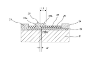
- FIG. 2 is a cross-sectional view of a horizontal semiconductor device according to the second embodiment of the present invention.
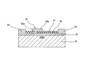
- FIG. 3 is a sectional view of a horizontal semiconductor device of a comparative example.
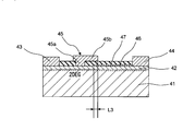
- FIG. 4 is a sectional view of a lateral semiconductor device according to the third embodiment of the present invention.
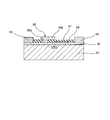
- FIG. 5 is a cross-sectional view of a horizontal semiconductor device according to the fourth embodiment of the present invention.
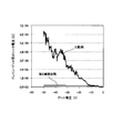
- FIG. 6 is a diagram showing drain-gate leakage current with respect to gate voltage of the lateral semiconductor device shown in FIGS.
- FIG. 7 is a diagram showing the gate current with respect to the gate voltage of the lateral semiconductor device of the second embodiment.
- FIG. 8 is a diagram showing the gate current with respect to the gate voltage of the horizontal semiconductor device of the comparative example.
- FIG. 9 is a sectional view of a horizontal semiconductor device according to the fifth embodiment of the present invention.
- FIG. 10 is a sectional view of a horizontal semiconductor device according to the sixth embodiment of the present invention.
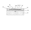
- FIG. 11 is a sectional view of a lateral semiconductor device according to the seventh embodiment of the present invention.
- FIG. 1 is a cross-sectional view of a lateral semiconductor device according to a first embodiment of the present invention.
- a lateral semiconductor device As an example of a lateral semiconductor device, a normally-on GaN HFET (Hetero-junction Field Effect Transistor) ).
- GaN HFET Hetero-junction Field Effect Transistor
- the lateral semiconductor device includes an undoped GaN layer 11 as an example of a first semiconductor layer and an example of a second semiconductor layer on an Si substrate (not shown).
- An undoped AlGaN layer 12 is sequentially formed. 2DEG (two-dimensional electron gas) is generated at the interface between the undoped GaN layer 11 and the undoped AlGaN layer 12.
- the GaN layer 11 and the AlGaN layer 12 constitute a nitride semiconductor layer.
- the substrate is not limited to the Si substrate, and a sapphire substrate or SiC substrate may be used.
- a nitride semiconductor layer may be grown on the sapphire substrate or SiC substrate, or an AlGaN layer is grown on the GaN substrate.
- a nitride semiconductor layer may be grown on a substrate made of a nitride semiconductor.
- a buffer layer may be appropriately formed between the substrate and each layer.
- a source electrode 13 and a drain electrode 14 are formed on the AlGaN layer 12 at a predetermined interval.
- a gate electrode 15 is formed between the source electrode 13 and the drain electrode 14 on the AlGaN layer 12 and on the source electrode 13 side.
- a first insulating film 16 is formed in a region on the AlGaN layer 12 except for a region in the vicinity of the gate electrode 15 between the gate electrode 15 and the drain electrode 14.
- a second insulating film 17 is formed on the region excluding the source electrode 13, the drain electrode 14, and the gate electrode 15. In FIG. 1, the second insulating film 17 is also formed on the first insulating film 16, but the second insulating film 17 may not be provided on the first insulating film 16.
- the thickness of the first insulating film 16 is 10 to 20 nm, and the thickness of the second insulating film 17 is 200 nm.
- the source electrode 13 and the drain electrode 14 are formed by ohmic electrodes on the AlGaN / GaN semiconductor surface, that is, the AlGaN layer 12 formed on the Si substrate (not shown).
- a film is formed as the first insulating film 16.
- the ratio of silicon Si is made larger than that of the stoichiometric silicon nitride film, thereby suppressing current collapse.
- the ratio of nitrogen is set higher than that in the first insulating film 16.
- an opening is formed by wet etching in the portion of the second insulating film 17 where the gate electrode 15 is to be formed by patterning using a resist.
- the opening is formed at a predetermined interval with respect to the first insulating film 16.
- a gate electrode 15 is formed by a Schottky electrode on the region of the AlGaN layer 12 exposed through the opening of the second insulating film 17.
- the first insulating film 16 for suppressing current collapse is set in advance with respect to the gate electrode 15 in the region on the AlGaN layer 12 and between the drain electrode 14 and the gate electrode 15. Formed on the AlGaN layer 12 and the first insulating film 16 so as to cover the end of the first insulating film 16 on the gate electrode 15 side and the lower portion of the gate electrode 15. A second insulating film 17 is formed so as to fill the region therebetween. As a result, the first insulating film 16 and the gate electrode 15 for suppressing current collapse are separated from each other, and between the end of the first insulating film 16 on the gate electrode 15 side and the lower portion of the gate electrode 15.
- the first insulating film 16 Since the second insulating film 17 is interposed, the first insulating film 16 causes a current collapse phenomenon (a phenomenon in which the on-resistance of the transistor in the high-voltage operation becomes higher than the on-resistance of the transistor in the low-voltage operation). While suppressing the leakage current, the leakage current flowing through the gate electrode 15 through the first insulating film 16 can be suppressed and the breakdown voltage can be improved.
- the second insulating film 17 having excellent insulating properties allows the gate electrode 15, the drain electrode 14, The leakage current during the period can be suppressed.
- FIG. 2 is a sectional view of a horizontal semiconductor device according to the second embodiment of the present invention.
- the lateral semiconductor device of the second embodiment has the same configuration as the lateral semiconductor device of the first embodiment except for the gate electrode.
- the lateral semiconductor device includes an undoped GaN layer 21 as an example of a first semiconductor layer and an example of a second semiconductor layer on a Si substrate (not shown).
- An undoped AlGaN layer 22 is formed in order.
- 2DEG two-dimensional electron gas
- a source electrode 23 and a drain electrode 24 are formed on the AlGaN layer 22 at a predetermined interval.
- a gate electrode 25 is formed between the source electrode 23 and the drain electrode 24 on the AlGaN layer 22 and on the source electrode 23 side.
- a first insulating film 26 is formed in a region excluding the region in the vicinity of the gate electrode 25 between the gate electrode 25 and the drain electrode 24 on the AlGaN layer 22.
- a second insulating film 27 that covers the first insulating film 26 is formed on a region excluding the source electrode 23, the drain electrode 24, and the gate electrode 25.
- the gate electrode 25 is formed of a base portion 25a and a field plate portion 25b formed above the base portion 25a.
- the length L1 (field plate length) of the field plate portion 25b protruding from the base portion 25a of the gate electrode 25 is 2 ⁇ m.
- FIG. 3 a horizontal semiconductor device (not shown) having a conventional structure in which the width of the portion where the second insulating film 27 is in contact with the horizontal semiconductor device is 0 ⁇ m is the same process.
- 31 is a GaN layer
- 32 is an AlGaN layer
- 33 is a source electrode
- 34 is a drain electrode
- 35 is a gate electrode
- 35a is a base
- 35b is a field plate portion
- 36 is a first insulating film
- 37 is a first insulating film. 2 insulating film.
- FIG. 6 shows the drain-gate leakage current with respect to the gate voltage of the lateral semiconductor device shown in FIGS.
- the horizontal axis represents the gate voltage [V]
- the vertical axis represents the drain-gate leakage current [A].
- the exponent base 10 is represented by the symbol E and the multiplication symbol x is omitted. For example, 1.0 ⁇ 10 ( ⁇ 05) is 1. E-05.
- the lateral semiconductor device shown in FIG. 2 of the second embodiment can significantly reduce the drain-gate leakage current as compared with the leakage current characteristic of the comparative example shown in FIG. did it.
- the current from the drain electrode 34 passes through 2DEG (two-dimensional electron gas) and the lower side of the gate electrode 35.
- a leak current path that flows to the gate electrode 35 through the first insulating film 36 due to a strong electric field in the vicinity of the gate electrode 35 under a high voltage is formed, and the leak current is considered to increase.
- the first insulating film 26 is formed at a distance from the gate electrode 25, and the gate electrode 25 of the first insulating film 26 is formed. Since the region between the end portion on the side and the lower portion (base portion 25a) of the gate electrode 25 is filled with the second insulating film 27, the gate electrode 25 is formed in the vicinity of the gate electrode 25 via the first insulating film 26. A flowing leakage current path is not formed, and the leakage current between the drain and the gate can be greatly reduced.
- FIG. 7 shows the gate current with respect to the gate voltage of the lateral semiconductor device of the second embodiment shown in FIG. 2
- FIG. 8 shows the gate current with respect to the gate voltage of the lateral semiconductor device of the comparative example shown in FIG. Yes.
- the horizontal axis represents the gate voltage [V]
- the vertical axis represents the gate current [A].
- the exponent base 10 is represented by the symbol E, and the multiplication symbol x is omitted. For example, 1.0 ⁇ 10 (-05) is 1. Represented by E-05.
- the second insulating film 27 is formed between the gate electrode 25 and the first insulating film 26, so that it exhibits a stable characteristic.
- a gate voltage-gate current curve was obtained.
- a leak current is generated in a state where the characteristic curve of the gate voltage-gate current of the lateral semiconductor device of the comparative example is disturbed, and it cannot be said that the current is stable.
- the first insulating film 26 that suppresses current collapse covers the gate electrode 25 so as to cover the region between the drain electrode 24 and the gate electrode 25 on the AlGaN layer 22. Since the first insulating film 26 and the gate electrode 25 for suppressing current collapse are separated from each other by forming a predetermined interval, current collapse phenomenon (in low voltage operation). (A phenomenon in which the on-resistance of the transistor in a high-voltage operation becomes higher than the on-resistance of the first transistor), while suppressing the leakage current flowing to the gate electrode 25 through the first insulating film 26 and reducing the withstand voltage. Can be improved.
- the field plate portion 25b formed on the AlGaN layer 22 so as to extend from the upper side of the base portion 25a of the gate electrode 25 to the drain electrode 24 side on the second insulating film 27 has a high voltage.
- the concentration of the electric field in the vicinity of the lower gate electrode 25 is relaxed, current collapse can be suppressed, and the breakdown voltage can be improved.
- the gate electrode 25 and the first insulating film 26 are separated by 0.5 ⁇ m, the gate electrode 25 and the first insulating film 26 are caused by manufacturing variation (positioning accuracy of the manufacturing apparatus is ⁇ 0.2 ⁇ m, for example).
- the gate electrode 25 and the first insulating film 26 are reliably separated from each other, and the gate electrode 25 and the first insulating film 26 are excellently insulated. By insulating with the two insulating films 27, the leakage current can be reliably suppressed while suppressing the current collapse phenomenon.
- FIG. 4 is a sectional view of a horizontal semiconductor device according to the third embodiment of the present invention.
- the lateral semiconductor device of the third embodiment has the same configuration as the lateral semiconductor device of the second embodiment except for the first insulating film.
- 41 is a GaN layer
- 42 is an AlGaN layer
- 43 is a source electrode
- 44 is a drain electrode
- 45 is a gate electrode
- 45a is a base
- 45b is a field plate portion
- 46 is a first insulating film
- 47 is a first insulating film. 2 insulating film.
- the difference between the lateral semiconductor device of the third embodiment and the lateral semiconductor device of the second embodiment is that the gate electrode 45 has a total length in the thickness direction of the first insulating film 46 and the second insulating film 47.
- the first insulating film 46 is formed on the AlGaN layer 42 below the field plate portion 45b. That is, the field plate portion 45 b of the gate electrode 45 and the first insulating film 46 overlap each other by a total length L 3 in the thickness direction of the first insulating film 46 and the second insulating film 47.
- the lateral semiconductor device of the third embodiment has the same effect as the lateral semiconductor device of the second embodiment.
- the first insulating film is provided below the field plate portion 45b, compared to the case where the first insulating film 46 is not provided below the field plate portion 45b of the gate electrode 45.
- the effect of suppressing the current collapse phenomenon can be increased.
- FIG. 5 shows a sectional view of a lateral semiconductor device according to the fourth embodiment of the present invention.
- the lateral semiconductor device of the fourth embodiment has the same configuration as that of the lateral semiconductor device of the second embodiment except for the first insulating film.
- 51 is a GaN layer
- 52 is an AlGaN layer
- 53 is a source electrode
- 54 is a drain electrode
- 55 is a gate electrode
- 55a is a base
- 55b is a field plate portion
- 56 is a first insulating film
- 57 is a first insulating film. 2 insulating film.
- the difference between the lateral semiconductor device of the fourth embodiment and the lateral semiconductor device of the second embodiment is that the field plate portion 55b of the gate electrode 55 and the first insulating film 56 do not overlap. That is, the first insulating film 56 is formed on the AlGaN layer 52 between the drain electrode 54 and the tip of the field plate portion 55 b of the gate electrode 55 on the drain electrode 54 side.
- the horizontal semiconductor device of the fourth embodiment has the same effect as the horizontal semiconductor device of the second embodiment.
- the first insulating film 56 is formed on the AlGaN layer 52 between the drain electrode 54 side end of the field plate portion 55b of the gate electrode 55 and the gate electrode 55, and the gate Since the field plate portion 55b of the electrode 55 and the first insulating film 56 do not overlap, a strong electric field is applied to the gate electrode 55 through the first insulating film 56 in the vicinity of the gate electrode 55 under a high voltage. It is difficult to form a flowing leakage current path, and the breakdown voltage can be further improved.
- the dielectric constant of the first insulating film 56 is higher than the dielectric constant of the second insulating film 57 in order to suppress the current collapse, the field plate portion 55b of the gate electrode 55 and the first insulating film 56 are By not overlapping, the capacity under the field plate portion 55b can be reduced, and the high frequency characteristics are improved.
- FIG. 9 shows a sectional view of a horizontal semiconductor device according to the fifth embodiment of the present invention.
- the lateral semiconductor device of the fifth embodiment is a GaN-based HFET as an example of a normally-off type recess lateral semiconductor device.
- the lateral semiconductor device includes an undoped GaN layer 61 as an example of a first semiconductor layer and an undoped AlGaN layer 62 as an example of a second semiconductor layer on an Si substrate (not shown). They are formed in order. 2DEG (two-dimensional electron gas) is generated at the interface between the undoped GaN layer 61 and the undoped AlGaN layer 62.
- the GaN layer 61 and the AlGaN layer 62 constitute a nitride semiconductor layer.
- the substrate is not limited to the Si substrate, and a sapphire substrate or SiC substrate may be used.
- a nitride semiconductor layer may be grown on the sapphire substrate or SiC substrate, or a GaN substrate.
- a nitride semiconductor layer may be grown on a substrate made of a nitride semiconductor, such as by growing an AlGaN layer.
- a source electrode 63 and a drain electrode 64 are formed on the AlGaN layer 62 at a predetermined interval.
- a recess 60 is provided in the upper part of the AlGaN layer 62.
- a silicon nitride film is formed as a first insulating film 66 on the AlGaN layer 62 excluding the recess 60, the source electrode 63 and the drain electrode 64.
- a silicon nitride film is formed as the second insulating film 67 so as to cover the first insulating film 66 and the recess 60.
- the gate electrode 65 is formed by the base portion 65a embedded in the concave portion 60 covered with the second insulating film 67 and the field plate portion 65b formed above the base portion 65a.
- the first insulating film 66 and the gate electrode 65 for suppressing current collapse are separated from each other, and the end of the first insulating film 66 on the gate electrode 65 side and the lower part of the gate electrode 65 ( A second insulating film 67 is interposed between the base 65a).
- the base 65 a of the gate electrode 65 is embedded in the recess 60 formed in a part on the upper side of the AlGaN layer 62, thereby forming a second interface formed at the heterointerface below the gate electrode 65. Since the threshold voltage is increased by decreasing the dimensional electron gas concentration, a normally-off operation is possible. Therefore, it is possible to realize a normally-off type HFET that suppresses a current collapse phenomenon and suppresses a leakage current to improve a withstand voltage.
- the first insulating film 66 that suppresses current collapse covers the gate electrode 65 so as to cover the region between the drain electrode 64 and the gate electrode 65 on the AlGaN layer 62. Since the first insulating film 66 and the gate electrode 65 for suppressing current collapse are spaced apart from each other, the current collapse phenomenon (in low voltage operation). (A phenomenon in which the on-resistance of the transistor in a high-voltage operation becomes higher than the on-resistance of the first transistor), and the leakage current flowing to the gate electrode 65 through the first insulating film 66 is suppressed to reduce the withstand voltage. Can be improved.
- the second insulating film 67 having excellent insulating properties allows the gate electrode 65, the drain electrode 64, Leakage current during the period can be suppressed.
- FIG. 10 shows a sectional view of a lateral semiconductor device according to the sixth embodiment of the present invention.
- the lateral semiconductor device according to the sixth embodiment is a GaN-based HFET as an example of a normally-off recess type lateral semiconductor device.
- the lateral semiconductor device includes an undoped GaN layer 71 as an example of a first semiconductor layer and an undoped AlGaN layer 72 as an example of a second semiconductor layer on an Si substrate (not shown). They are formed in order. 2DEG (two-dimensional electron gas) is generated at the interface between the undoped GaN layer 71 and the undoped AlGaN layer 72.
- 2DEG two-dimensional electron gas
- a source electrode 73 and a drain electrode 74 are formed on the AlGaN layer 72 at a predetermined interval.
- a recess 70 is provided in a part of the upper side of the GaN layer 71 through the AlGaN layer 72.
- a first insulating film 76 is formed on the AlGaN layer 72 excluding the recess 70, the source electrode 73 and the drain electrode 74.
- a second insulating film 77 is formed so as to cover the first insulating film 76 and the recess 70.
- a gate electrode 75 is formed by a base portion 75a embedded in the recess 70 covered with the second insulating film 77 and a field plate portion 75b formed on the base portion 75a.
- the first insulating film 76 and the gate electrode 75 for suppressing current collapse are separated from each other, and the end of the first insulating film 76 on the gate electrode 75 side and the lower part of the gate electrode 75 ( A second insulating film 67 is interposed between the base 75a).
- the base portion 75 a of the gate electrode 75 is embedded in the concave portion 70 that penetrates the AlGaN layer 72 and is formed in a part on the upper side of the GaN layer 71.
- the hetero interface between the layer 71 and the AlGaN layer 72 is cut off, 2DEG (two-dimensional electron gas) does not exist, and the threshold voltage increases, so that a normally-off operation is possible. Therefore, it is possible to realize a normally-off type HFET that suppresses a current collapse phenomenon and suppresses a leakage current to improve a withstand voltage.
- the horizontal semiconductor device of the sixth embodiment has the same effects as the horizontal semiconductor device of the fifth embodiment.
- FIG. 11 is a sectional view of a lateral semiconductor device according to the seventh embodiment of the present invention.
- the lateral semiconductor device according to the seventh embodiment has the same configuration as the lateral semiconductor device according to the second embodiment except for the third insulating film.
- the lateral semiconductor device of the seventh embodiment includes an undoped GaN layer 81 as an example of a first semiconductor layer and an example of a second semiconductor layer on a Si substrate (not shown).
- An undoped AlGaN layer 82 is formed in order. 2DEG (two-dimensional electron gas) is generated at the interface between the undoped GaN layer 81 and the undoped AlGaN layer 82.
- a source electrode 83 and a drain electrode 84 are formed on the AlGaN layer 82 at a predetermined interval.
- a gate electrode 85 is formed between the source electrode 83 and the drain electrode 84 on the AlGaN layer 82 and on the source electrode 83 side.
- a first insulating film 86 is formed in a region excluding the region in the vicinity of the gate electrode 85 between the gate electrode 85 and the drain electrode 84 on the AlGaN layer 82.
- a second insulating film 87 that covers the first insulating film 86 is formed.
- a third insulating film 88 is formed so as to cover the second insulating film 87 and the region where the base portion 85a of the gate electrode 85 of the AlGaN layer 82 is formed.
- the third insulating film 88 is made of SiN (or SiO 2 or Al 2 O 3 or the like) having a thickness of 10 to 40 nm.
- the gate electrode 85 includes a base portion 85a and a field plate portion 85b formed on the base portion 85a.
- a field plate portion 85b projects from the base portion 85a of the gate electrode 85 toward the drain electrode 84 side.
- the lateral semiconductor device of the seventh embodiment can be manufactured by adding a step of forming the third insulating film 88 to the manufacturing process described in the lateral semiconductor device of the first embodiment.
- the first insulating film 86 is formed at a distance from the gate electrode 85, the end of the first insulating film 86 on the gate electrode 85 side, and the gate electrode 85. Since the region between the lower portion (base portion 85a) of the first and second bases is filled with the second insulating film 87, a leakage current path that flows to the gate electrode 85 through the first insulating film 86 in the vicinity of the gate electrode 35 is formed. Thus, the leakage current between the drain and the gate can be greatly reduced.
- the silicon nitride film is used as the first insulating film.
- the present invention is not limited to this, and a film made of TaOx, SiO 2 , HfOx, or the like may be used.
- the silicon nitride film is used in the second insulating film is not limited thereto, TaOx, SiO 2, HfOx, film or of SiOC or the like, BCB (benzocyclobutene Organic materials such as) may be used.
- the GaN layers 11, 21, 41, 51, 61, 71, 81 and the AlGaN layers 12, 22, 42, 52, 62, 72, 82 are stacked on the substrate.
- a lateral semiconductor device including a nitride semiconductor layer has been described, the structure of the nitride semiconductor layer is not limited to this, and the present invention is applied to a lateral semiconductor device including a nitride semiconductor layer including a contact layer and a cap layer. May be.
- the source electrodes 13, 23, 43, 53, 63, 73, 83 are provided on the AlGaN layers 12, 22, 42, 52, 62, 72, 82 at predetermined intervals.
- the horizontal semiconductor device in which the drain electrodes 14, 24, 44, 54, 64, 74, and 84 are formed has been described. However, at least a part is formed in the nitride semiconductor layer, and the source electrode,
- the present invention may be applied to a horizontal semiconductor device in which a drain electrode is formed. That is, in the lateral semiconductor device of the present invention, the source electrode and the drain electrode are all formed on the nitride semiconductor layer with a space therebetween, and the nitride semiconductor layer is spaced from each other by etching.
- the source electrode and drain electrode are all formed in each recess, and further, two recesses are formed spaced apart from each other by etching the nitride semiconductor layer.
- the source electrode and the drain electrode are formed so that a part of the lower side of the source electrode and the drain electrode is embedded in each recess.
- One of the source electrode and the drain electrode may be entirely formed on the nitride semiconductor layer, and the other of the source electrode or the drain electrode may be at least partially formed in the nitride semiconductor layer.
- the second insulating films 17, 27, 47, 57, 67, 74, 84 are formed on the first insulating films 16, 26, 46, 56, 66, 76, 86.
- the horizontal semiconductor device in which the gate electrode is formed has been described. However, a second insulating film is formed on the first insulating film to fill a region between the gate electrode side end of the first insulating film and the gate electrode.
- a lateral semiconductor device that is not formed, or a second insulating film that fills a region between the gate electrode side end of the first insulating film and the gate electrode is connected to the gate electrode side of the first insulating film.
- the present invention may be applied to a horizontal semiconductor device or the like formed on a part of the region.
- the nitride semiconductor of the lateral semiconductor device of the present invention may be any material represented by Al x In y Ga 1-xy N (x ⁇ 0, y ⁇ 0, 0 ⁇ x + y ⁇ 1).
- the lateral semiconductor device of the present invention is not limited to the HFET of the first to seventh embodiments, but may be a field effect transistor having another configuration.
Landscapes
- Junction Field-Effect Transistors (AREA)
- Insulated Gate Type Field-Effect Transistor (AREA)
- Electrodes Of Semiconductors (AREA)
Abstract
GaN層(11)とAlGaN層(12)と、AlGaN層(12)上に間隔をあけて形成されたソース電極(13)およびドレイン電極(14)と、AlGaN層(12)上かつソース電極(13)とドレイン電極(14)との間に形成されたゲート電極(15)と、AlGaN層(12)上かつドレイン電極(13)とゲート電極(15)との間の領域に、ゲート電極(15)に対して予め設定された間隔をあけて形成された電流コラプスを抑制するための第1の絶縁膜(16)と、第1の絶縁膜(16)のゲート電極(15)側の端部とゲート電極(15)との間の領域を埋めるように形成された第2の絶縁膜(17)と備える。電流コラプス現象を抑えつつ、リーク電流を抑制して耐圧を向上できる横型半導体装置を提供する。
Description
この発明は、横型半導体装置に関し、詳しくは、窒化物半導体層上にソース電極とドレイン電極およびゲート電極が形成された横型半導体装置に関する。
従来、横型半導体装置としては、窒化物半導体層上に離間してソース電極とドレイン電極が形成され、そのソース電極とドレイン電極との間にゲート電極が形成され、窒化物半導体層上に第1の絶縁膜と第2の絶縁膜が積層された電界効果トランジスタがある(例えば、特開2004-200248号公報(特許文献1)参照)。
この電界効果トランジスタは、ゲート電極がフィールドプレート構造であり、第1の絶縁膜をSiNで形成することにより電流コラプスを抑えようとしている。
しかしながら、上記構成の電界効果トランジスタでは、電流コラプス現象を抑えることができても、高電圧下ではリーク電流が生じて耐圧が低下するという問題が依然としてある。
そこで、この発明の課題は、電流コラプス現象を抑えつつ、リーク電流を抑制して耐圧を向上できる横型半導体装置を提供することにある。
上記課題を解決するため、この発明の横型半導体装置は、
窒化物半導体層と、
上記窒化物半導体層上に、または、上記窒化物半導体層内に少なくとも一部が形成されると共に、互いに間隔をあけて形成されたソース電極およびドレイン電極と、
上記ソース電極と上記ドレイン電極との間に形成されたゲート電極と、
上記窒化物半導体層上、かつ、上記ドレイン電極と上記ゲート電極との間の領域に、上記ゲート電極に対して予め設定された間隔をあけて形成された電流コラプスを抑制するための第1の絶縁膜と、
少なくとも、上記第1の絶縁膜の上記ゲート電極側の端部と上記ゲート電極との間の領域を埋めるように形成された第2の絶縁膜と
を備えたことを特徴とする。
窒化物半導体層と、
上記窒化物半導体層上に、または、上記窒化物半導体層内に少なくとも一部が形成されると共に、互いに間隔をあけて形成されたソース電極およびドレイン電極と、
上記ソース電極と上記ドレイン電極との間に形成されたゲート電極と、
上記窒化物半導体層上、かつ、上記ドレイン電極と上記ゲート電極との間の領域に、上記ゲート電極に対して予め設定された間隔をあけて形成された電流コラプスを抑制するための第1の絶縁膜と、
少なくとも、上記第1の絶縁膜の上記ゲート電極側の端部と上記ゲート電極との間の領域を埋めるように形成された第2の絶縁膜と
を備えたことを特徴とする。
ここで、「電流コラプス」とは、低電圧動作でのトランジスタのオン抵抗と比べて高電圧動作でのトランジスタのオン抵抗が高くなってしまう現象である。
上記構成によれば、電流コラプスを抑制する第1の絶縁膜が、窒化物半導体層上かつドレイン電極とゲート電極との間の領域に、ゲート電極に対して予め設定された間隔をあけて形成され、少なくとも、窒化物半導体層上の第1の絶縁膜のゲート電極側とゲート電極との間の領域を埋めるように第2の絶縁膜が形成されていることによって、電流コラプスを抑制するための第1の絶縁膜とゲート電極とが離間し、その第1の絶縁膜のゲート電極側の端部とゲート電極との間に第2の絶縁膜が介在するので、第1の絶縁膜により電流コラプス現象を抑えつつ、第1の絶縁膜を介してゲート電極に流れるリーク電流を抑制して耐圧を向上できる。なお、上記ソース電極およびドレイン電極は、窒化物半導体層上に互いに間隔をあけて形成してもよいし、窒化物半導体層内に少なくとも一部が埋め込まれるようにかつ互いに間隔をあけて形成してもよい。
また、一実施形態の横型半導体装置では、
上記第2の絶縁膜は、上記第1の絶縁膜の少なくとも上記ゲート電極側の端部上に位置する部分を含み、
上記ゲート電極は、上記窒化物半導体層上に形成された基部と、上記基部の上側から上記ドレイン電極側に向かって上記第2の絶縁膜上に延在するように形成されたフィールドプレート部とを有する。
上記第2の絶縁膜は、上記第1の絶縁膜の少なくとも上記ゲート電極側の端部上に位置する部分を含み、
上記ゲート電極は、上記窒化物半導体層上に形成された基部と、上記基部の上側から上記ドレイン電極側に向かって上記第2の絶縁膜上に延在するように形成されたフィールドプレート部とを有する。
上記実施形態によれば、窒化物半導体層上に形成されたゲート電極の基部の上側からドレイン電極側に向かって第2の絶縁膜上に延在するようにフィールドプレート部を形成することによって、高電圧下でのゲート電極近傍の電界集中が緩和され、電流コラプスを抑制できると共に耐圧を向上できる。
また、一実施形態の横型半導体装置では、
上記第1の絶縁膜は、上記ゲート電極の上記フィールドプレート部の上記ドレイン電極側の先端と上記ドレイン電極との間の上記窒化物半導体層上に形成されている。
上記第1の絶縁膜は、上記ゲート電極の上記フィールドプレート部の上記ドレイン電極側の先端と上記ドレイン電極との間の上記窒化物半導体層上に形成されている。
上記実施形態によれば、ゲート電極のフィールドプレート部のドレイン電極側の先端とドレイン電極との間の窒化物半導体層上に第1の絶縁膜が形成され、ゲート電極のフィールドプレート部と第1の絶縁膜とがオーバーラップしていないことによって、高電圧下でのゲート電極近傍で強い電界により第1の絶縁膜を介してゲート電極に流れるリーク電流経路が形成されにくくなり、耐圧をさらに向上できる。また、電流コラプスを抑制するために第1の絶縁膜の誘電率が第2の絶縁膜の誘電率よりも高いので、ゲート電極のフィールドプレート部と第1の絶縁膜とがオーバーラップしないことによりフィールドプレート部下側の容量を低減でき、高周波特性が向上する。
また、一実施形態の横型半導体装置では、
上記第1の絶縁膜は、上記ゲート電極の上記フィールドプレート部の上記ドレイン電極側の先端から上記ゲート電極の上記基部側に向かって、少なくとも上記第1の絶縁膜と上記第2の絶縁膜の厚さ方向の合計長さ分、上記フィールドプレート部の下側に形成されている。
上記第1の絶縁膜は、上記ゲート電極の上記フィールドプレート部の上記ドレイン電極側の先端から上記ゲート電極の上記基部側に向かって、少なくとも上記第1の絶縁膜と上記第2の絶縁膜の厚さ方向の合計長さ分、上記フィールドプレート部の下側に形成されている。
上記実施形態によれば、ゲート電極のフィールドプレート部の下側に第1の絶縁膜がない場合よりも、フィールドプレート部の下側に第1の絶縁膜を形成することにより、電流コラプス現象を抑制する効果を大きくできる。
また、一実施形態の横型半導体装置では、
上記第1の絶縁膜は、ストイキオメトリなシリコン窒化膜よりもシリコンの比率が高いシリコン窒化膜である。
上記第1の絶縁膜は、ストイキオメトリなシリコン窒化膜よりもシリコンの比率が高いシリコン窒化膜である。
ここで、「ストイキオメトリなシリコン窒化膜」とは、SiとNが3:4の組成の膜である。
上記実施形態によれば、ストイキオメトリなシリコン窒化膜よりもシリコンの比率が高いシリコン窒化膜を第1の絶縁膜に用いることによって、電流コラプスを抑制することが可能になる。
また、一実施形態の横型半導体装置では、
上記第2の絶縁膜は、上記第1の絶縁膜より窒素の比率が高いシリコン窒化膜である。
上記第2の絶縁膜は、上記第1の絶縁膜より窒素の比率が高いシリコン窒化膜である。
上記実施形態によれば、第1の絶縁膜よりも窒素の比率が高いシリコン窒化膜を第2の絶縁膜に用いることによって、絶縁性に優れた第2の絶縁膜によりゲート電極とドレイン電極との間のリーク電流を抑制できる。
また、一実施形態の横型半導体装置では、
上記窒化物半導体層は、基板上に順に積層された第1半導体層およびその第1半導体層とヘテロ界面を形成する第2半導体層を含み、
上記第1半導体層と上記第2半導体層とのヘテロ界面に形成された2次元電子ガスを利用するヘテロ接合電界効果トランジスタが形成されており、
上記窒化物半導体層の上側の一部に形成された凹部に上記ゲート電極の少なくとも一部が埋め込まれている。
上記窒化物半導体層は、基板上に順に積層された第1半導体層およびその第1半導体層とヘテロ界面を形成する第2半導体層を含み、
上記第1半導体層と上記第2半導体層とのヘテロ界面に形成された2次元電子ガスを利用するヘテロ接合電界効果トランジスタが形成されており、
上記窒化物半導体層の上側の一部に形成された凹部に上記ゲート電極の少なくとも一部が埋め込まれている。
上記実施形態によれば、窒化物半導体層の上側の一部に形成された凹部にゲート電極の少なくとも一部が埋め込まれていることによって、ゲート電極下のヘテロ界面に形成される二次元電子ガス濃度を低下させるか、または、ゲート電極により窒化物半導体層のヘテロ界面が遮断されて2次元電子ガスが存在しないことにより、閾値電圧が高くなるので、ヘテロ接合電界効果トランジスタのノーマリーオフ動作が可能になる。したがって、電流コラプス現象を抑えつつ、リーク電流を抑制して耐圧を向上できるノーマリーオフ動作のヘテロ接合電界効果トランジスタを実現できる。
以上より明らかなように、この発明の横型半導体装置によれば、電流コラプス現象を抑えつつ、リーク電流を抑制して耐圧を向上できる横型半導体装置を実現することができる。
以下、この発明の横型半導体装置を図示の実施の形態により詳細に説明する。
〔第1実施形態〕
図1はこの発明の第1実施形態の横型半導体装置の断面図を示しており、横型半導体装置の一例としてのノーマリーオンタイプのGaN系HFET(Hetero-junction Field Effect Transistor;ヘテロ接合電界効果トランジスタ)である。
図1はこの発明の第1実施形態の横型半導体装置の断面図を示しており、横型半導体装置の一例としてのノーマリーオンタイプのGaN系HFET(Hetero-junction Field Effect Transistor;ヘテロ接合電界効果トランジスタ)である。
この第1実施形態の横型半導体装置は、図1に示すように、Si基板(図示せず)上に、第1半導体層の一例としてのアンドープGaN層11と、第2半導体層の一例としてのアンドープAlGaN層12を順に形成している。このアンドープGaN層11とアンドープAlGaN層12との界面に2DEG(2次元電子ガス)が発生する。このGaN層11とAlGaN層12で窒化物半導体層を構成している。なお、上記基板は、Si基板に限らず、サファイヤ基板やSiC基板を用いてもよく、サファイヤ基板やSiC基板上に窒化物半導体層を成長させてもよいし、GaN基板にAlGaN層を成長させる等のように、窒化物半導体からなる基板上に窒化物半導体層を成長させてもよい。また、適宜、バッファ層を基板と各層間に形成してもよい。
AlGaN層12上に、所定の間隔をあけてソース電極13とドレイン電極14を形成している。そのAlGaN層12上のソース電極13とドレイン電極14との間かつソース電極13側にゲート電極15を形成している。そして、AlGaN層12上のゲート電極15とドレイン電極14との間のゲート電極15近傍の領域を除く領域に第1の絶縁膜16を形成している。ソース電極13とドレイン電極14とゲート電極15を除く領域上に、第2の絶縁膜17を形成している。なお、図1では、第1の絶縁膜16上にも第2の絶縁膜17を形成しているが、第1の絶縁膜16上に第2の絶縁膜17は無くともよい。
この第1実施形態では、第1の絶縁膜16の膜厚は10~20nmであり、第2の絶縁膜17の膜厚は200nmである。
上記横型半導体装置の製造方法を以下に説明する。
まず、Si基板(図示せず)上に形成されたAlGaN/GaN半導体表面すなわちAlGaN層12上にオーミック電極によりソース電極13,ドレイン電極14を形成する。
その後、そのソース電極13とドレイン電極14との間に、プラズマCVD(Chemical Vapor Deposition:化学的気相成長)法によりガス流量比N2/NH3/SiH4=645sccm/85sccm/70sccmでシリコン窒化膜を第1の絶縁膜16として形成する。この第1の絶縁膜16では、ストイキオメトリなシリコン窒化膜よりもシリコンSiの比率を大きくしており、これにより電流コラプスを抑制する。
次に、レジストを用いたパターニングにより、第1の絶縁膜16となるシリコン窒化膜のゲート電極15を形成する部分近傍の領域およびそのゲート電極15を形成する部分とソース電極13との間の領域にウェットエッチングで開口部を形成する。
さらに、ソース電極13,ドレイン電極14を除く領域上に、プラズマCVD法によりガス流量比N2/NH3/SiH4=697sccm/92.5sccm/10.5sccmでシリコン窒化膜を第2の絶縁膜17として形成している。この第2の絶縁膜17では、第1の絶縁膜16よりも窒素の比率を高くしている。
再度、レジストを用いたパターニングにより、第2の絶縁膜17のゲート電極15を形成する部分にウェットエッチングで開口部を形成する。この開口部は、第1の絶縁膜16に対して所定の間隔をあけて形成する。
その後、第2の絶縁膜17の開口部により露出したAlGaN層12の領域上に、ショットキー電極によりゲート電極15を形成する。
上記構成の横型半導体装置によれば、電流コラプスを抑制する第1の絶縁膜16が、AlGaN層12上かつドレイン電極14とゲート電極15との間の領域に、ゲート電極15に対して予め設定された間隔をあけて形成され、AlGaN層12上および第1の絶縁膜16上を覆うように、かつ、第1の絶縁膜16のゲート電極15側の端部とゲート電極15の下部との間の領域を埋めるように第2の絶縁膜17が形成されている。これによって、電流コラプスを抑制するための第1の絶縁膜16とゲート電極15とが離間し、その第1の絶縁膜16のゲート電極15側の端部とゲート電極15の下部との間に第2の絶縁膜17が介在するので、第1の絶縁膜16により電流コラプス現象(低電圧動作でのトランジスタのオン抵抗と比べて高電圧動作でのトランジスタのオン抵抗が高くなってしまう現象)を抑えつつ、第1の絶縁膜16を介してゲート電極15に流れるリーク電流を抑制して耐圧を向上できる。
また、ストイキオメトリなシリコン窒化膜よりもシリコンの比率が高いシリコン窒化膜を第1の絶縁膜16に用いることによって、電流コラプスを抑制することが可能になる。
また、第1の絶縁膜16よりも窒素の比率が高いシリコン窒化膜を第2の絶縁膜17に用いることによって、絶縁性に優れた第2の絶縁膜17によりゲート電極15とドレイン電極14との間のリーク電流を抑制できる。
〔第2実施形態〕
図2はこの発明の第2実施形態の横型半導体装置の断面図を示している。この第2実施形態の横型半導体装置は、ゲート電極を除いて第1実施形態の横型半導体装置と同一の構成をしている。
図2はこの発明の第2実施形態の横型半導体装置の断面図を示している。この第2実施形態の横型半導体装置は、ゲート電極を除いて第1実施形態の横型半導体装置と同一の構成をしている。
この第2実施形態の横型半導体装置は、図2に示すように、Si基板(図示せず)上に、第1半導体層の一例としてのアンドープGaN層21と、第2半導体層の一例としてのアンドープAlGaN層22を順に形成している。このアンドープGaN層21とアンドープAlGaN層22との界面に2DEG(2次元電子ガス)が発生する。
AlGaN層22上に、所定の間隔をあけてソース電極23とドレイン電極24を形成している。そのAlGaN層22上のソース電極23とドレイン電極24との間かつソース電極23側にゲート電極25を形成している。そして、AlGaN層22上のゲート電極25とドレイン電極24との間のゲート電極25近傍の領域を除く領域に第1の絶縁膜26を形成している。ソース電極23とドレイン電極24とゲート電極25を除く領域上に、第1の絶縁膜26を覆う第2の絶縁膜27を形成している。
上記ゲート電極25は、基部25aと、その基部25aの上部に形成されたフィールドプレート部25bで形成されている。このゲート電極25の基部25aから張り出しているフィールドプレート部25bの長さL1(フィールドプレート長)を2μmとしている。また、第2の絶縁膜27がAlGaN層22と接している部分の幅を0.5μmとしている。すなわち、ゲート電極25の基部25aと第1の絶縁膜26とは0.5μm(=L2)離間している。
また、比較例として、図3に示すように、第2の絶縁膜27が横型半導体装置と接している部分の幅が0μmとなる従来構造の横型半導体装置(図示せず)も同様のプロセスで作製した。図3において、31はGaN層、32はAlGaN層、33はソース電極、34はドレイン電極、35はゲート電極、35aは基部、35bはフィールドプレート部、36は第1の絶縁膜、37は第2の絶縁膜である。
図2,図3に示す2つの横型半導体装置の電気的測定を行って比較した。この測定条件は、ソース電極23,33とドレイン電極24,34と基板を0Vとし、ゲート電極25,35に0Vから-50Vまで負電圧を印加した。
図6は図2,図3に示す横型半導体装置のゲート電圧に対するドレイン-ゲート間のリーク電流を示している。図6において、横軸はゲート電圧[V]を表し、縦軸はドレイン-ゲート間のリーク電流[A]を表す。なお、図6中の縦軸の浮動小数点形式の表現では、指数底10は記号Eで表しかつ掛け算記号×は省略しており、例えば、1.0×10(-05乗)は、1.E-05で表わされる。
図6に示すように、この第2実施形態の図2に示す横型半導体装置は、図3に示す比較例のリーク電流特性に比べて、ドレイン-ゲート間のリーク電流を大幅に低減することができた。
図3に示す比較例の横型半導体装置では、ゲート電極35に印加する負電圧の絶対値が大きくなるほど、ドレイン電極34からの電流が2DEG(2次元電子ガス)を通ってゲート電極35の下側近傍まで流れて、高電圧下でのゲート電極35近傍で強い電界により第1の絶縁膜36を介してゲート電極35に流れるリーク電流経路が形成され、リーク電流が大きくなるものと考えられる。
これに対して、図2に示す第2実施形態の横型半導体装置では、ゲート電極25に対して間隔をあけて第1の絶縁膜26が形成され、その第1の絶縁膜26のゲート電極25側の端部とゲート電極25の下部(基部25a)との間の領域を第2の絶縁膜27で埋めているため、ゲート電極25近傍で第1の絶縁膜26を介してゲート電極25に流れるようなリーク電流経路が形成されず、ドレイン-ゲート間のリーク電流を大幅に低減することができる。
また、図7は図2に示す第2実施形態の横型半導体装置のゲート電圧に対するゲート電流を示しており、図8は図3に示す比較例の横型半導体装置のゲート電圧に対するゲート電流を示している。図7,図8において、横軸はゲート電圧[V]を表し、縦軸はゲート電流[A]を表す。なお、図7,図8の縦軸の浮動小数点形式の表現では、指数底10は記号Eで表しかつ掛け算記号×は省略しており、例えば、1.0×10(-05乗)は、1.E-05で表わされる。
図7に示すように、第2実施形態の横型半導体装置では、第2の絶縁膜27がゲート電極25と第1の絶縁膜26の間に形成されることで、安定した特性を示すなだらかなゲート電圧-ゲート電流曲線が得られた。これに対して、図8に示すように、比較例の横型半導体装置のゲート電圧-ゲート電流の特性曲線が乱れた状態でリーク電流が生じており、安定しているとは言えない。
上記構成の横型半導体装置によれば、電流コラプスを抑制する第1の絶縁膜26が、AlGaN層22上のドレイン電極24とゲート電極25との間の領域を覆うように、ゲート電極25に対して予め設定された間隔をあけて形成されていることによって、電流コラプスを抑制するための第1の絶縁膜26とゲート電極25とが離間していることにより、電流コラプス現象(低電圧動作でのトランジスタのオン抵抗と比べて高電圧動作でのトランジスタのオン抵抗が高くなってしまう現象)を抑えつつ、第1の絶縁膜26を介してゲート電極25に流れるリーク電流を抑制して耐圧を向上できる。
また、AlGaN層22上に形成されたゲート電極25の基部25aの上側からドレイン電極24側に向かって第2の絶縁膜27上に延在するように形成されたフィールドプレート部25bによって、高電圧下でのゲート電極25近傍の電界集中が緩和され、電流コラプスを抑制できると共に耐圧を向上できる。
また、ゲート電極25と第1の絶縁膜26とが0.5μm離間していることによって、製造ばらつき(製造装置の位置決め精度は例えば±0.2μm)によりゲート電極25と第1の絶縁膜26とが接触または近接する恐れがなくなり、ゲート電極25と第1の絶縁膜26とを確実に離間させ、さらに、そのゲート電極25と第1の絶縁膜26との間を絶縁性に優れた第2の絶縁膜27で絶縁することによって、電流コラプス現象を抑えつつ、リーク電流を確実に抑制することができる。
〔第3実施形態〕
図4はこの発明の第3実施形態の横型半導体装置の断面図を示している。この第3実施形態の横型半導体装置は、第1の絶縁膜を除いて第2実施形態の横型半導体装置と同一の構成をしている。図4において、41はGaN層、42はAlGaN層、43はソース電極、44はドレイン電極、45はゲート電極、45aは基部、45bはフィールドプレート部、46は第1の絶縁膜、47は第2の絶縁膜である。
図4はこの発明の第3実施形態の横型半導体装置の断面図を示している。この第3実施形態の横型半導体装置は、第1の絶縁膜を除いて第2実施形態の横型半導体装置と同一の構成をしている。図4において、41はGaN層、42はAlGaN層、43はソース電極、44はドレイン電極、45はゲート電極、45aは基部、45bはフィールドプレート部、46は第1の絶縁膜、47は第2の絶縁膜である。
この第3実施形態の横型半導体装置と第2実施形態の横型半導体装置との相違点は、第1の絶縁膜46と第2の絶縁膜47の厚さ方向の合計長さ分、ゲート電極45のフィールドプレート部45bの下側のAlGaN層42上に第1の絶縁膜46が形成されている点である。すなわち、ゲート電極45のフィールドプレート部45bと第1の絶縁膜46とが、第1の絶縁膜46と第2の絶縁膜47の厚さ方向の合計長さL3だけオーバーラップしている。
上記第3実施形態の横型半導体装置は、第2実施形態の横型半導体装置と同様の効果を有する。
上記第3実施形態の横型半導体装置によれば、ゲート電極45のフィールドプレート部45bの下側に第1の絶縁膜46がない場合よりも、フィールドプレート部45bの下側に第1の絶縁膜46を形成することにより、電流コラプス現象を抑制する効果を大きくできる。
〔第4実施形態〕
図5はこの発明の第4実施形態の横型半導体装置の断面図を示している。この第4実施形態の横型半導体装置は、第1の絶縁膜を除いて第2実施形態の横型半導体装置と同一の構成をしている。図5において、51はGaN層、52はAlGaN層、53はソース電極、54はドレイン電極、55はゲート電極、55aは基部、55bはフィールドプレート部、56は第1の絶縁膜、57は第2の絶縁膜である。
図5はこの発明の第4実施形態の横型半導体装置の断面図を示している。この第4実施形態の横型半導体装置は、第1の絶縁膜を除いて第2実施形態の横型半導体装置と同一の構成をしている。図5において、51はGaN層、52はAlGaN層、53はソース電極、54はドレイン電極、55はゲート電極、55aは基部、55bはフィールドプレート部、56は第1の絶縁膜、57は第2の絶縁膜である。
この第4実施形態の横型半導体装置と第2実施形態の横型半導体装置との相違点は、ゲート電極55のフィールドプレート部55bと第1の絶縁膜56とがオーバーラップしていない点である。すなわち、第1の絶縁膜56は、ゲート電極55のフィールドプレート部55bのドレイン電極54側の先端とドレイン電極54との間のAlGaN層52上に形成されている。
上記第4実施形態の横型半導体装置は、第2実施形態の横型半導体装置と同様の効果を有する。
上記構成の横型半導体装置によれば、ゲート電極55のフィールドプレート部55bのドレイン電極54側の先端とドレイン電極54との間のAlGaN層52上に第1の絶縁膜56を形成して、ゲート電極55のフィールドプレート部55bと第1の絶縁膜56とがオーバーラップしていないことによって、高電圧下でのゲート電極55近傍で強い電界により第1の絶縁膜56を介してゲート電極55に流れるリーク電流経路が形成されにくくなり、耐圧をさらに向上できる。また、電流コラプスを抑制するために第1の絶縁膜56の誘電率が第2の絶縁膜57の誘電率よりも高いので、ゲート電極55のフィールドプレート部55bと第1の絶縁膜56とがオーバーラップしないことによりフィールドプレート部55b下側の容量を低減でき、高周波特性が向上する。
〔第5実施形態〕
図9はこの発明の第5実施形態の横型半導体装置の断面図を示している。この第5実施形態の横型半導体装置は、ノーマリーオフタイプのリセス型の横型半導体装置の一例としてのGaN系HFETである。
図9はこの発明の第5実施形態の横型半導体装置の断面図を示している。この第5実施形態の横型半導体装置は、ノーマリーオフタイプのリセス型の横型半導体装置の一例としてのGaN系HFETである。
この横型半導体装置は、図9に示すように、Si基板(図示せず)上に、第1半導体層の一例としてのアンドープGaN層61と、第2半導体層の一例としてのアンドープAlGaN層62を順に形成している。このアンドープGaN層61とアンドープAlGaN層62との界面に2DEG(2次元電子ガス)が発生する。このGaN層61とAlGaN層62で窒化物半導体層を構成している。上記第1実施形態と同様に、基板は、Si基板に限らず、サファイヤ基板やSiC基板を用いてもよく、サファイヤ基板やSiC基板上に窒化物半導体層を成長させてもよいし、GaN基板にAlGaN層を成長させる等のように、窒化物半導体からなる基板上に窒化物半導体層を成長させてもよい。
AlGaN層62上に、所定の間隔をあけてソース電極63とドレイン電極64を形成している。ソース電極63とドレイン電極64との間のソース電極63側に、AlGaN層62の上部に凹部60を設けている。その凹部60とソース電極63とドレイン電極64を除くAlGaN層62上に、第1の絶縁膜66としてシリコン窒化膜を形成している。第1の絶縁膜66および凹部60を覆うように、第2の絶縁膜67としてシリコン窒化膜を形成している。そして、第2の絶縁膜67で覆われた凹部60内に埋め込まれた基部65aと、その基部65aの上部に形成されたフィールドプレート部65bでゲート電極65を形成している。
上記横型半導体装置では、電流コラプスを抑制するための第1の絶縁膜66とゲート電極65とが離間し、その第1の絶縁膜66のゲート電極65側の端部とゲート電極65の下部(基部65a)との間に第2の絶縁膜67が介在している。
図9に示す横型半導体装置では、AlGaN層62の上側の一部に形成された凹部60にゲート電極65の基部65aが埋め込まれていることによって、ゲート電極65下のヘテロ界面に形成される二次元電子ガス濃度を低下させて閾値電圧を高くするので、ノーマリーオフ動作が可能になる。したがって、電流コラプス現象を抑えつつ、リーク電流を抑制して耐圧を向上したノーマリーオフタイプのHFETを実現することができる。
上記構成の横型半導体装置によれば、電流コラプスを抑制する第1の絶縁膜66が、AlGaN層62上のドレイン電極64とゲート電極65との間の領域を覆うように、ゲート電極65に対して予め設定された間隔をあけて形成されていることによって、電流コラプスを抑制するための第1の絶縁膜66とゲート電極65とが離間していることにより、電流コラプス現象(低電圧動作でのトランジスタのオン抵抗と比べて高電圧動作でのトランジスタのオン抵抗が高くなってしまう現象)を抑えつつ、第1の絶縁膜66を介してゲート電極65に流れるリーク電流を抑制して耐圧を向上できる。
また、ストイキオメトリなシリコン窒化膜よりもシリコンの比率が高いシリコン窒化膜を第1の絶縁膜66に用いることによって、電流コラプスを抑制することが可能になる。
また、第1の絶縁膜66よりも窒素の比率が高いシリコン窒化膜を第2の絶縁膜67に用いることによって、絶縁性に優れた第2の絶縁膜67によりゲート電極65とドレイン電極64との間のリーク電流を抑制することができる。
〔第6実施形態〕
図10はこの発明の第6実施形態の横型半導体装置の断面図を示している。この第6実施形態の横型半導体装置は、ノーマリーオフタイプのリセス型の横型半導体装置の一例としてのGaN系HFETである。
図10はこの発明の第6実施形態の横型半導体装置の断面図を示している。この第6実施形態の横型半導体装置は、ノーマリーオフタイプのリセス型の横型半導体装置の一例としてのGaN系HFETである。
この横型半導体装置は、図10に示すように、Si基板(図示せず)上に、第1半導体層の一例としてのアンドープGaN層71と、第2半導体層の一例としてのアンドープAlGaN層72を順に形成している。このアンドープGaN層71とアンドープAlGaN層72との界面に2DEG(2次元電子ガス)が発生する。
AlGaN層72上に、所定の間隔をあけてソース電極73とドレイン電極74を形成している。ソース電極73とドレイン電極74との間のソース電極73側に、AlGaN層72を貫通してGaN層71の上側の一部に凹部70を設けている。その凹部70とソース電極73とドレイン電極74を除くAlGaN層72に第1の絶縁膜76を形成している。第1の絶縁膜76および凹部70を覆うように第2の絶縁膜77を形成している。そして、第2の絶縁膜77で覆われた凹部70内に埋め込まれた基部75aと、その基部75aの上部に形成されたフィールドプレート部75bでゲート電極75を形成している。
上記横型半導体装置では、電流コラプスを抑制するための第1の絶縁膜76とゲート電極75とが離間し、その第1の絶縁膜76のゲート電極75側の端部とゲート電極75の下部(基部75a)との間に第2の絶縁膜67が介在している。
図10に示す横型半導体装置では、AlGaN層72を貫通してGaN層71の上側の一部に形成された凹部70にゲート電極75の基部75aが埋め込まれていることによって、ゲート電極75によりGaN層71とAlGaN層72とのヘテロ界面が遮断されて2DEG(2次元電子ガス)が存在せず、閾値電圧が高くなるので、ノーマリーオフ動作が可能になる。したがって、電流コラプス現象を抑えつつ、リーク電流を抑制して耐圧を向上したノーマリーオフタイプのHFETを実現することができる。
上記第6実施形態の横型半導体装置は、第5実施形態の横型半導体装置と同様の効果を有する。
〔第7実施形態〕
図11はこの発明の第7実施形態の横型半導体装置の断面図を示している。この第7実施形態の横型半導体装置は、第3の絶縁膜を除いて第2実施形態の横型半導体装置と同一の構成をしている。
図11はこの発明の第7実施形態の横型半導体装置の断面図を示している。この第7実施形態の横型半導体装置は、第3の絶縁膜を除いて第2実施形態の横型半導体装置と同一の構成をしている。
この第7実施形態の横型半導体装置は、図11に示すように、Si基板(図示せず)上に、第1半導体層の一例としてのアンドープGaN層81と、第2半導体層の一例としてのアンドープAlGaN層82を順に形成している。このアンドープGaN層81とアンドープAlGaN層82との界面に2DEG(2次元電子ガス)が発生する。
AlGaN層82上に、所定の間隔をあけてソース電極83とドレイン電極84を形成している。そのAlGaN層82上のソース電極83とドレイン電極84との間かつソース電極83側にゲート電極85を形成している。そして、AlGaN層82上のゲート電極85とドレイン電極84との間のゲート電極85近傍の領域を除く領域に第1の絶縁膜86を形成している。ソース電極83とドレイン電極84とゲート電極85を除く領域上に、第1の絶縁膜86を覆う第2の絶縁膜87を形成している。
さらに、第2の絶縁膜87上およびAlGaN層82のゲート電極85の基部85aが形成される領域上を覆うように、第3の絶縁膜88を形成している。この第3の絶縁膜88は、厚さ10~40nmのSiN(またはSiO2やAl2O3等)からなる。
上記ゲート電極85は、基部85aと、その基部85aの上部に形成されたフィールドプレート部85bで形成されている。このゲート電極85の基部85aからドレイン電極84側に向かってフィールドプレート部85bが張り出している。
この第7実施形態の横型半導体装置は、第1実施形態の横型半導体装置で説明した製造工程に第3の絶縁膜88を形成する工程を追加することにより製造できる。
上記第7実施形態の横型半導体装置では、ゲート電極85に対して間隔をあけて第1の絶縁膜86が形成され、その第1の絶縁膜86のゲート電極85側の端部とゲート電極85の下部(基部85a)との間の領域を第2の絶縁膜87で埋めているため、ゲート電極35近傍で第1の絶縁膜86を介してゲート電極85に流れるようなリーク電流経路が形成されず、ドレイン-ゲート間のリーク電流を大幅に低減することができる。
上記第1~第7実施形態では、第1の絶縁膜にシリコン窒化膜を用いたが、これに限らず、TaOx、SiO2、HfOx等からなる膜を用いてもよい。
また、上記第1~第7実施形態では、第2の絶縁膜にシリコン窒化膜を用いたが、これに限らず、TaOx、SiO2、HfOx、SiOC等からなる膜や、BCB(ベンゾシクロブテン)などの有機材料を用いてもよい。
また、上記第1~第7実施形態では、基板上にGaN層11,21,41,51,61,71,81とAlGaN層12,22,42,52,62,72,82とを積層した窒化物半導体層を備えた横型半導体装置について説明したが、窒化物半導体層の構造はこれに限らず、コンタクト層やキャップ層などを含む窒化物半導体層を備えた横型半導体装置にこの発明を適用してもよい。
また、上記第1~第7実施形態では、AlGaN層12,22,42,52,62,72,82上に所定の間隔をあけてソース電極13,23,43,53,63,73,83とドレイン電極14,24,44,54,64,74,84を形成した横型半導体装置について説明したが、窒化物半導体層内に少なくとも一部が形成されると共に、互いに間隔をあけてソース電極,ドレイン電極が形成された横型半導体装置にこの発明を適用してもよい。
すなわち、この発明の横型半導体装置では、窒化物半導体層上に互いに間隔をあけてソース電極,ドレイン電極の全部が形成されている場合と、窒化物半導体層をエッチングすることにより互いに間隔をあけて2つの凹部を形成して、その各凹部内にソース電極,ドレイン電極の全部が形成されている場合と、さらに、窒化物半導体層をエッチングすることにより互いに間隔をあけて2つの凹部を形成して、その各凹部内にソース電極,ドレイン電極の下側の一部が埋め込まれるように、ソース電極,ドレイン電極が形成されている場合がある。なお、ソース電極またはドレイン電極の一方は、窒化物半導体層上に全部が形成され、ソース電極またはドレイン電極の他方は、窒化物半導体層内に少なくとも一部が形成されていてもよい。
すなわち、この発明の横型半導体装置では、窒化物半導体層上に互いに間隔をあけてソース電極,ドレイン電極の全部が形成されている場合と、窒化物半導体層をエッチングすることにより互いに間隔をあけて2つの凹部を形成して、その各凹部内にソース電極,ドレイン電極の全部が形成されている場合と、さらに、窒化物半導体層をエッチングすることにより互いに間隔をあけて2つの凹部を形成して、その各凹部内にソース電極,ドレイン電極の下側の一部が埋め込まれるように、ソース電極,ドレイン電極が形成されている場合がある。なお、ソース電極またはドレイン電極の一方は、窒化物半導体層上に全部が形成され、ソース電極またはドレイン電極の他方は、窒化物半導体層内に少なくとも一部が形成されていてもよい。
また、上記第1~第7実施形態では、第1の絶縁膜16,26,46,56,66,76,86上に第2の絶縁膜17,27,47,57,67,74,84が形成されている横型半導体装置について説明したが、第1の絶縁膜のゲート電極側の端部とゲート電極との間の領域を埋める第2の絶縁膜が第1の絶縁膜上には形成されていない横型半導体装置や、第1の絶縁膜のゲート電極側の端部とゲート電極との間の領域を埋める第2の絶縁膜が、その領域に連なる第1の絶縁膜のゲート電極側の一部の領域上に形成されている横型半導体装置などにこの発明を適用してもよい。
この発明の横型半導体装置の窒化物半導体は、AlxInyGa1-x-yN(x≧0、y≧0、0≦x+y≦1)で表されるものであればよい。
また、この発明の横型半導体装置は、上記第1~第7実施形態のHFETに限らず、他の構成の電界効果トランジスタであってもよい。
この発明の具体的な実施の形態について説明したが、この発明は上記第1~第6実施形態に限定されるものではなく、この発明の範囲内で種々変更して実施することができる。
11,21,31,41,51,61,71,81…GaN層
12,22,32,42,52,62,72,82…AlGaN層
13,23,33,43,53,63,73,83…ソース電極
14,24,34,44,54,64,74,84…ドレイン電極
15,25,35,45,55,65,75,85…ゲート電極
16,26,36,46,56,66,76,86…第1の絶縁膜
17,27,37,47,57,67,77,87…第2の絶縁膜
25a,35a,45a,55a,65a,75a,85a…基部
25b,35b,45b,55b,65b,75b,85b…フィールドプレート部
60,70…凹部
12,22,32,42,52,62,72,82…AlGaN層
13,23,33,43,53,63,73,83…ソース電極
14,24,34,44,54,64,74,84…ドレイン電極
15,25,35,45,55,65,75,85…ゲート電極
16,26,36,46,56,66,76,86…第1の絶縁膜
17,27,37,47,57,67,77,87…第2の絶縁膜
25a,35a,45a,55a,65a,75a,85a…基部
25b,35b,45b,55b,65b,75b,85b…フィールドプレート部
60,70…凹部
Claims (7)
- 窒化物半導体層と、
上記窒化物半導体層上に、または、上記窒化物半導体層内に少なくとも一部が形成されると共に、互いに間隔をあけて形成されたソース電極(13,23,43,53,63,73,83)およびドレイン電極(14,24,44,54,64,74,84)と、
上記ソース電極(13,23,43,53,63,73,83)と上記ドレイン電極(14,24,44,54,64,74,84)との間に形成されたゲート電極(15,25,45,55,65,75,85)と、
上記窒化物半導体層上、かつ、上記ドレイン電極(14,24,44,54,64,74,84)と上記ゲート電極(15,25,45,55,65,75,85)との間の領域に、上記ゲート電極(15,25,45,55,65,75,85)に対して予め設定された間隔をあけて形成された電流コラプスを抑制するための第1の絶縁膜(16,26,46,56,66,76,86)と、
少なくとも、上記第1の絶縁膜(16,26,46,56,66,76,86)の上記ゲート電極(15,25,45,55,65,75,85)側の端部と上記ゲート電極(15,25,45,55,65,75,85)との間の領域を埋めるように形成された第2の絶縁膜(17,27,47,57,67,77,87)と
を備えたことを特徴とする横型半導体装置。 - 請求項1に記載の横型半導体装置において、
上記第2の絶縁膜(17,27,47,57,67,77,87)は、上記第1の絶縁膜(16,26,46,56,66,76,86)の少なくとも上記ゲート電極(15,25,45,55,65,75,85)側の端部上に位置する部分を含み、
上記ゲート電極(15,25,45,55,65,75,85)は、上記窒化物半導体層上に形成された基部(25a,45a,54a,64a,75a,85a)と、上記基部(25a,45a,54a,64a,75a,85a)の上側から上記ドレイン電極(14,24,44,54,64,74,84)側に向かって上記第2の絶縁膜(17,27,47,57,67,77,87)上に延在するように形成されたフィールドプレート部(25b,45b,54b,64b,75b,85b)とを有することを特徴とする横型半導体装置。 - 請求項2に記載の横型半導体装置において、
上記第1の絶縁膜(16,26,46,56,66,76,86)は、上記ゲート電極(15,25,45,55,65,75,85)の上記フィールドプレート部(25b,45b,54b,64b,75b,85b)の上記ドレイン電極(14,24,44,54,64,74,84)側の先端と上記ドレイン電極(14,24,44,54,64,74,84)との間の上記窒化物半導体層上に形成されていることを特徴とする横型半導体装置。 - 請求項2に記載の横型半導体装置において、
上記第1の絶縁膜(16,26,46,56,66,76,86)は、上記ゲート電極(15,25,45,55,65,75,85)の上記フィールドプレート部(25b,45b,54b,64b,75b,85b)の上記ドレイン電極(14,24,44,54,64,74,84)側の先端から上記ゲート電極(15,25,45,55,65,75,85)の上記基部(25a,45a,54a,64a,75a,85a)側に向かって、少なくとも上記第1の絶縁膜(16,26,46,56,66,76,86)と上記第2の絶縁膜(17,27,47,57,67,77,87)の厚さ方向の合計長さ分、上記フィールドプレート部(25b,45b,54b,64b,75b,85b)の下側に形成されていることを特徴とする横型半導体装置。 - 請求項1から4までのいずれか1つに記載の横型半導体装置において、
上記第1の絶縁膜(16,26,46,56,66,76,86)は、ストイキオメトリなシリコン窒化膜よりもシリコンの比率が高いシリコン窒化膜であることを特徴とする横型半導体装置。 - 請求項5に記載の横型半導体装置において、
上記第2の絶縁膜(17,27,47,57,67,77,87)は、上記第1の絶縁膜(16,26,46,56,66,76,86)よりも窒素の比率が高いシリコン窒化膜であることを特徴とする横型半導体装置。 - 請求項1から6までのいずれか1つに記載の横型半導体装置において、
上記窒化物半導体層は、基板上に順に積層された第1半導体層(61,71)およびその第1半導体層(61,71)とヘテロ界面を形成する第2半導体層(62,72)を含み、
上記第1半導体層(61,71)と上記第2半導体層(62,72)とのヘテロ界面に形成された2次元電子ガスを利用するヘテロ接合電界効果トランジスタが形成されており、
上記窒化物半導体層の上側の一部に形成された凹部(60,70)に上記ゲート電極(65,75)の少なくとも一部が埋め込まれていることを特徴とする横型半導体装置。
Applications Claiming Priority (2)
| Application Number | Priority Date | Filing Date | Title |
|---|---|---|---|
| JP2011-030045 | 2011-02-15 | ||
| JP2011030045A JP2014078537A (ja) | 2011-02-15 | 2011-02-15 | 横型半導体装置 |
Publications (1)
| Publication Number | Publication Date |
|---|---|
| WO2012111363A1 true WO2012111363A1 (ja) | 2012-08-23 |
Family
ID=46672306
Family Applications (1)
| Application Number | Title | Priority Date | Filing Date |
|---|---|---|---|
| PCT/JP2012/050425 Ceased WO2012111363A1 (ja) | 2011-02-15 | 2012-01-12 | 横型半導体装置 |
Country Status (2)
| Country | Link |
|---|---|
| JP (1) | JP2014078537A (ja) |
| WO (1) | WO2012111363A1 (ja) |
Cited By (8)
| Publication number | Priority date | Publication date | Assignee | Title |
|---|---|---|---|---|
| JP2014138110A (ja) * | 2013-01-17 | 2014-07-28 | Fujitsu Ltd | 半導体装置及びその製造方法、電源装置、高周波増幅器 |
| WO2014129245A1 (ja) * | 2013-02-21 | 2014-08-28 | シャープ株式会社 | 窒化物半導体装置 |
| JP2014187084A (ja) * | 2013-03-22 | 2014-10-02 | Toshiba Corp | 半導体装置およびその製造方法 |
| CN104112772A (zh) * | 2013-04-18 | 2014-10-22 | 富士通株式会社 | 化合物半导体器件及其制造方法 |
| CN104425487A (zh) * | 2013-09-10 | 2015-03-18 | 株式会社东芝 | 半导体器件 |
| WO2020142345A3 (en) * | 2019-01-03 | 2020-08-13 | Cree, Inc. | High electron mobility transistors having improved drain current drift and/or leakage current performance |
| CN115458580A (zh) * | 2021-06-08 | 2022-12-09 | 株式会社东芝 | 半导体装置 |
| US11658233B2 (en) | 2019-11-19 | 2023-05-23 | Wolfspeed, Inc. | Semiconductors with improved thermal budget and process of making semiconductors with improved thermal budget |
Families Citing this family (6)
| Publication number | Priority date | Publication date | Assignee | Title |
|---|---|---|---|---|
| JP6191660B2 (ja) | 2014-08-05 | 2017-09-06 | 株式会社豊田中央研究所 | 熱伝導体、熱伝導体を備える半導体装置 |
| FR3031239B1 (fr) * | 2014-12-30 | 2023-04-28 | Thales Sa | Passivation multicouche de la face superieure de l'empilement de materiaux semi-conducteurs d'un transistor a effet de champ. |
| WO2017051688A1 (ja) * | 2015-09-22 | 2017-03-30 | 株式会社デンソー | 半導体装置 |
| JP6701767B2 (ja) | 2015-09-22 | 2020-05-27 | 株式会社デンソー | 半導体装置 |
| JP6536318B2 (ja) | 2015-09-24 | 2019-07-03 | 三菱電機株式会社 | 半導体装置及びその製造方法 |
| JP7726758B2 (ja) * | 2021-06-08 | 2025-08-20 | 株式会社東芝 | 半導体装置 |
Citations (6)
| Publication number | Priority date | Publication date | Assignee | Title |
|---|---|---|---|---|
| JP2004200248A (ja) * | 2002-12-16 | 2004-07-15 | Nec Corp | 電界効果トランジスタ |
| JP2004214471A (ja) * | 2003-01-07 | 2004-07-29 | Nec Corp | 電界効果トランジスタ |
| WO2007040160A1 (ja) * | 2005-09-30 | 2007-04-12 | Nec Corporation | 電界効果トランジスタ |
| JP2008205392A (ja) * | 2007-02-22 | 2008-09-04 | Fujitsu Ltd | 半導体装置及びその製造方法 |
| JP2009164300A (ja) * | 2007-12-28 | 2009-07-23 | Fujitsu Ltd | 半導体装置及びその製造方法 |
| JP2010238982A (ja) * | 2009-03-31 | 2010-10-21 | Fujitsu Ltd | 化合物半導体装置及びその製造方法 |
-
2011
- 2011-02-15 JP JP2011030045A patent/JP2014078537A/ja not_active Withdrawn
-
2012
- 2012-01-12 WO PCT/JP2012/050425 patent/WO2012111363A1/ja not_active Ceased
Patent Citations (6)
| Publication number | Priority date | Publication date | Assignee | Title |
|---|---|---|---|---|
| JP2004200248A (ja) * | 2002-12-16 | 2004-07-15 | Nec Corp | 電界効果トランジスタ |
| JP2004214471A (ja) * | 2003-01-07 | 2004-07-29 | Nec Corp | 電界効果トランジスタ |
| WO2007040160A1 (ja) * | 2005-09-30 | 2007-04-12 | Nec Corporation | 電界効果トランジスタ |
| JP2008205392A (ja) * | 2007-02-22 | 2008-09-04 | Fujitsu Ltd | 半導体装置及びその製造方法 |
| JP2009164300A (ja) * | 2007-12-28 | 2009-07-23 | Fujitsu Ltd | 半導体装置及びその製造方法 |
| JP2010238982A (ja) * | 2009-03-31 | 2010-10-21 | Fujitsu Ltd | 化合物半導体装置及びその製造方法 |
Cited By (16)
| Publication number | Priority date | Publication date | Assignee | Title |
|---|---|---|---|---|
| JP2014138110A (ja) * | 2013-01-17 | 2014-07-28 | Fujitsu Ltd | 半導体装置及びその製造方法、電源装置、高周波増幅器 |
| WO2014129245A1 (ja) * | 2013-02-21 | 2014-08-28 | シャープ株式会社 | 窒化物半導体装置 |
| JP2014187084A (ja) * | 2013-03-22 | 2014-10-02 | Toshiba Corp | 半導体装置およびその製造方法 |
| US9337300B2 (en) | 2013-03-22 | 2016-05-10 | Kabushiki Kaisha Toshiba | Nitride-based semiconductor device |
| US9184273B2 (en) | 2013-04-18 | 2015-11-10 | Fujitsu Limited | Compound semiconductor device and method of manufacturing the same |
| US20140312362A1 (en) * | 2013-04-18 | 2014-10-23 | Fujitsu Limited | Compound semiconductor device and method of manufacturing the same |
| JP2014212214A (ja) * | 2013-04-18 | 2014-11-13 | 富士通株式会社 | 化合物半導体装置及びその製造方法 |
| EP2793269A1 (en) * | 2013-04-18 | 2014-10-22 | Fujitsu Limited | Compound semiconductor device and method of manufacturing the same |
| CN104112772A (zh) * | 2013-04-18 | 2014-10-22 | 富士通株式会社 | 化合物半导体器件及其制造方法 |
| CN104425487A (zh) * | 2013-09-10 | 2015-03-18 | 株式会社东芝 | 半导体器件 |
| WO2020142345A3 (en) * | 2019-01-03 | 2020-08-13 | Cree, Inc. | High electron mobility transistors having improved drain current drift and/or leakage current performance |
| US10937873B2 (en) | 2019-01-03 | 2021-03-02 | Cree, Inc. | High electron mobility transistors having improved drain current drift and/or leakage current performance |
| US11355600B2 (en) | 2019-01-03 | 2022-06-07 | Wolfspeed, Inc. | High electron mobility transistors having improved drain current drift and/or leakage current performance |
| US11658233B2 (en) | 2019-11-19 | 2023-05-23 | Wolfspeed, Inc. | Semiconductors with improved thermal budget and process of making semiconductors with improved thermal budget |
| CN115458580A (zh) * | 2021-06-08 | 2022-12-09 | 株式会社东芝 | 半导体装置 |
| CN115458580B (zh) * | 2021-06-08 | 2025-12-09 | 株式会社东芝 | 半导体装置 |
Also Published As
| Publication number | Publication date |
|---|---|
| JP2014078537A (ja) | 2014-05-01 |
Similar Documents
| Publication | Publication Date | Title |
|---|---|---|
| WO2012111363A1 (ja) | 横型半導体装置 | |
| US9620599B2 (en) | GaN-based semiconductor transistor | |
| US9406792B2 (en) | Semiconductor device having GaN-based layer | |
| JP5348364B2 (ja) | ヘテロ接合型電界効果半導体装置 | |
| US9837524B2 (en) | Semiconductor device and method of manufacturing semiconductor device | |
| JP6251071B2 (ja) | 半導体装置 | |
| CN102237402B (zh) | 氮化物半导体元件 | |
| US10204995B2 (en) | Normally off HEMT with self aligned gate structure | |
| US8222675B2 (en) | Nitride semiconductor device including gate insulating portion containing AIN | |
| US9761682B2 (en) | Semiconductor device with silicon nitride film on nitride semiconductor layer and manufacturing method thereof | |
| US10784361B2 (en) | Semiconductor device and method for manufacturing the same | |
| CN105280695A (zh) | 半导体装置与其的制造方法 | |
| JP2017073506A (ja) | 窒化物半導体装置およびその製造方法 | |
| CN102623498A (zh) | 半导体元件 | |
| JP2010153493A (ja) | 電界効果半導体装置及びその製造方法 | |
| JP2011204717A (ja) | 化合物半導体装置 | |
| JP2015046444A (ja) | 半導体装置 | |
| JP6496149B2 (ja) | 半導体装置および半導体装置の製造方法 | |
| CN104916679A (zh) | 半导体装置 | |
| TW201737395A (zh) | 半導體裝置及半導體裝置的製造方法 | |
| US10373833B2 (en) | Semiconductor device and method for manufacturing the same | |
| WO2014003058A1 (ja) | 窒化物半導体装置の電極構造および窒化物半導体電界効果トランジスタ | |
| JP2013229458A (ja) | ヘテロ接合電界効果型トランジスタおよびその製造方法 | |
| JP6313509B2 (ja) | 半導体装置 |
Legal Events
| Date | Code | Title | Description |
|---|---|---|---|
| 121 | Ep: the epo has been informed by wipo that ep was designated in this application |
Ref document number: 12747473 Country of ref document: EP Kind code of ref document: A1 |
|
| NENP | Non-entry into the national phase |
Ref country code: DE |
|
| 122 | Ep: pct application non-entry in european phase |
Ref document number: 12747473 Country of ref document: EP Kind code of ref document: A1 |
|
| NENP | Non-entry into the national phase |
Ref country code: JP |