WO2012111257A1 - 固体撮像素子および電子情報機器 - Google Patents
固体撮像素子および電子情報機器 Download PDFInfo
- Publication number
- WO2012111257A1 WO2012111257A1 PCT/JP2012/000399 JP2012000399W WO2012111257A1 WO 2012111257 A1 WO2012111257 A1 WO 2012111257A1 JP 2012000399 W JP2012000399 W JP 2012000399W WO 2012111257 A1 WO2012111257 A1 WO 2012111257A1
- Authority
- WO
- WIPO (PCT)
- Prior art keywords
- light receiving
- plan
- transfer
- view
- transfer electrode
- Prior art date
- Legal status (The legal status is an assumption and is not a legal conclusion. Google has not performed a legal analysis and makes no representation as to the accuracy of the status listed.)
- Ceased
Links
Images




Classifications
-
- H—ELECTRICITY
- H10—SEMICONDUCTOR DEVICES; ELECTRIC SOLID-STATE DEVICES NOT OTHERWISE PROVIDED FOR
- H10F—INORGANIC SEMICONDUCTOR DEVICES SENSITIVE TO INFRARED RADIATION, LIGHT, ELECTROMAGNETIC RADIATION OF SHORTER WAVELENGTH OR CORPUSCULAR RADIATION
- H10F39/00—Integrated devices, or assemblies of multiple devices, comprising at least one element covered by group H10F30/00, e.g. radiation detectors comprising photodiode arrays
- H10F39/80—Constructional details of image sensors
- H10F39/802—Geometry or disposition of elements in pixels, e.g. address-lines or gate electrodes
Definitions
- the present invention relates to a solid-state imaging device provided with a plurality of light-receiving units that photoelectrically convert image light from a subject and to image, and a digital video camera and a digital still, for example, using the solid-state imaging device as an image input device in an imaging unit
- the present invention relates to an electronic information device such as a digital camera such as a camera, an image input camera such as a surveillance camera, a scanner device, a facsimile device, a television telephone device, and a mobile phone device with a camera.
- This type of conventional solid-state image sensor is a two-pixel shared CCD solid-state image sensor, and a plurality of light receiving elements in a vertical row are arranged on the left and right sides of a vertical transfer unit that transfers signal charges.
- a configuration in which one vertical transfer unit is provided for a plurality of pixels in two columns is repeatedly arranged in the row direction.
- one vertical transfer unit is reduced by one vertical transfer unit for a plurality of pixels in two columns.
- the light receiving area of each light receiving element can be increased, or the pixel size can be reduced and the number of pixels can be increased without reducing the light receiving sensitivity and dynamic range while maintaining the light receiving area of each light receiving element. I am letting.
- FIG. 8 is a partial plan view schematically showing a configuration example of a main part of a conventional solid-state imaging device disclosed in Patent Document 1.
- a conventional solid-state imaging device 100 includes a plurality of light receiving elements 101 arranged in a matrix in the column direction and the row direction, an opening 102 through which each light receiving element 101 is exposed to enter light, and a light receiving function.
- a channel stop 103 for preventing intrusion of signal charges between pixels adjacent to each other in the horizontal transfer direction of the element 101, and a signal charge from each of a plurality of light receiving elements 101 in a vertical column located on both sides to read out the signal charges.
- a vertical transfer unit 104 for transferring the signal charges, and a charge transfer for reading the signal charges of the light receiving element 101 to the vertical transfer unit 104 and transferring the signal charges along the vertical transfer unit 104 in the vertical direction (column direction). Transfer electrodes 105 to 107 for applying a control signal are provided.
- the transfer electrodes 107 and 106 (vertical transfer unit 104), the light receiving element 101, the channel stop 103, the light receiving element 101, and the transfer electrodes 107 and 106 (vertical transfer unit 104) are arranged in the row direction (lateral direction). Are arranged in this order.
- the transfer electrode 105, the light receiving element 101, the transfer electrodes 105 to 107, the light receiving element 101, and the transfer electrodes 105 to 107 are arranged in this order in the column direction (vertical direction).
- a plurality of light receiving elements 101 are respectively positioned in the column direction on both sides of each vertical transfer unit 104, and signal charges are alternately read from the light receiving elements 101 on both sides to the middle vertical transfer unit 104.
- the light receiving elements 101 in the same row are adjacent to each other through the channel stop 103.
- the transfer electrode 105 is made of polysilicon of the first layer and is formed so as to extend in the horizontal transfer direction between the light receiving elements 101 adjacent to each other in the vertical transfer direction. Along one side) and extending in a comb-like shape.
- the transfer electrode 106 is made of polysilicon of the second layer, and is formed so as to extend in the horizontal transfer direction between the light receiving elements 101 adjacent in the vertical transfer direction, and on one side (here, the vertical transfer unit 104) In the half width of the right side, a portion extending in a comb shape is formed on the upper side (the other side along the vertical transfer direction).
- the transfer electrode 107 is made of third-layer polysilicon and is formed so as to extend in the horizontal transfer direction between the light receiving elements 101 adjacent to each other in the vertical transfer direction. It has a portion extending in a comb-like shape on the upper side (the other side along the vertical transfer direction) in the half width of the left side.
- each light receiving element 101 includes a transfer electrode 105 made of polysilicon of the first layer, a transfer electrode 106 made of polysilicon of the second layer, and a transfer electrode made of polysilicon of the third layer.
- An opening 102 is formed by being surrounded by the electrode 107.
- Each comb-like portion of each transfer electrode 106 is a portion that performs read-out driving for reading out signal charges from the right light receiving element 101 to the vertical transfer portion 104 underneath.
- each comb-like portion of each transfer electrode 107 is a portion that performs readout driving for reading signal charges from the light receiving element 101 on the left side to the vertical transfer unit 104 therebelow.
- Patent Document 2 as in the configuration of Patent Document 1, a conventional solid-state imaging device has a plurality of light receiving elements arranged in a matrix in the column direction and the row direction. A plurality of light receiving elements in a vertical row are arranged on both sides of the vertical transfer unit. This configuration is repeated in the row direction. The signal charges from the light receiving elements on both sides are alternately read out to the vertical transfer unit between them, and transferred in the vertical direction along the vertical transfer unit.
- the present invention solves the above-described conventional problems.
- the light receiving sensitivity and dynamic range of the light receiving region are maintained while maintaining the light receiving area of each light receiving element.
- a solid-state imaging device capable of further reducing the pixel size and increasing the number of pixels without causing a reduction, and a solid-state imaging device using the solid-state imaging device as an image input device in an imaging unit such as a mobile phone device with a camera
- An object is to provide electronic information equipment.
- the solid-state imaging device is a two-pixel shared configuration solid-state imaging device in which a plurality of vertical rows of light receiving elements are arranged on both sides of a vertical transfer unit that transfers signal charges.
- An opening region for incident light is provided between each transfer electrode wiring adjacent in view and between each vertical transfer portion orthogonal to and adjacent in plan view, and 2 columns ⁇ n rows in the open region (N is a plurality) 2 ⁇ n light receiving elements are arranged, and signal charges are alternately read into the vertical transfer unit from the light receiving elements in the same row arranged on both sides of the vertical transfer unit and transferred. Therefore, the above object can be achieved.
- the 2 ⁇ n light receiving elements of 2 columns ⁇ n rows (n is a plurality) in the solid-state imaging device of the present invention are 4 light receiving elements of 2 columns ⁇ 2 rows or 2 columns ⁇ 3. Each of the six light receiving elements in the row.
- a channel stop portion for preventing signal charges from entering between the upper, lower, left and right sides of the light receiving element in the opening region of the solid-state imaging device of the present invention is provided between the light receiving elements on the semiconductor substrate. Is provided.
- a plurality of charge transfer control signals for reading signal charges from the light receiving elements to the vertical transfer unit in the solid-state imaging device according to the present invention and transferring the charges in the vertical direction along the vertical transfer units are applied.
- a transfer electrode and a plurality of transfer electrode wirings respectively connected thereto are provided. That is, a plurality of transfer electrodes to which a charge transfer control signal for reading out signal charges from the light receiving elements to the vertical transfer unit and transferring charges in the vertical direction along the vertical transfer unit are applied to the transfer electrode wiring
- the transfer electrode wirings are electrically connected to the plurality of transfer electrodes, respectively.
- the transfer electrode wiring has three layers, and the first-layer transfer electrode wiring has a comb-shaped first transfer electrode extending in a right-angled triangular shape with an acute angle on the upper side in plan view on the vertical transfer portion.
- the transfer electrode wiring of the second layer has a comb-like second transfer electrode that extends in the shape of a right triangle with an acute angle on the lower side in plan view on the vertical transfer part, and is half-width and on the upper side in plan view.
- the transfer electrode wiring of the third layer has a portion extending in a comb shape on the upper side in plan view on the vertical transfer portion, and the comb-shaped portion is a right triangle island in plan view via a contact plug therebelow.
- the third-layer transfer electrode wiring that is electrically connected to the third transfer electrode having a half width and that is on the lower side in the plan view has a plan view on the vertical transfer portion.
- the comb-like portion is electrically connected to the fourth transfer electrode in the shape of a right-angled triangular island in plan view via a contact plug therebelow.
- the signal charges are read from the light receiving elements adjacent to the vertical transfer portion through the side portions of the right and left triangles in plan view of the second transfer electrode and the fourth transfer electrode, respectively, and the second row is the first row
- the signal charge is read from the light receiving element adjacent to the vertical transfer portion through the side portions of the right-angled triangle in plan view of the transfer electrode and the third transfer electrode.
- the transfer electrode wiring has four layers, and the first-layer transfer electrode wiring has a comb-shaped first transfer electrode extending in a right-angled triangular shape with a sharp tip on the upper side in plan view on the vertical transfer portion.
- the transfer electrode wiring of the second layer has a comb-like second transfer electrode that extends in the shape of a right triangle with an acute angle on the lower side in plan view on the vertical transfer part, and is half-width and on the upper side in plan view.
- the transfer electrode wiring of the third layer has a portion extending in a comb shape on the upper side in plan view on the vertical transfer portion, and the comb-shaped portion is a right triangle island in plan view via a contact plug therebelow.
- the third-layer transfer electrode wiring that is electrically connected to the third transfer electrode having a half width and that is on the lower side in the plan view has a plan view on the vertical transfer portion.
- the comb-like portion is electrically connected to the fourth transfer electrode in the shape of a right-angled triangular island in plan view via a contact plug thereunder, and is half-width and on the upper side in plan view.
- the transfer electrode wiring of the fourth layer has a portion extending in a comb shape on the upper side in plan view on the vertical transfer portion, and the comb-shaped portion is a right triangle island in plan view via a contact plug therebelow
- the fourth-layer transfer electrode wiring that is electrically connected to the fifth transfer electrode having a half width and that is on the lower side in plan view has a portion extending in a comb-like shape on the lower side in plan view on the vertical transfer portion.
- the comb-like portion is electrically connected to the sixth transfer electrode having a right-angled triangular island shape in plan view via a contact plug therebelow, and the first row includes the second transfer electrode and the fourth transfer electrode.
- the electronic information device of the present invention uses the solid-state imaging device of the present invention as an image input device in an imaging unit, and thereby achieves the above object.
- an opening region for incident light that is surrounded between the transfer electrode wirings adjacent in a plan view and between the vertical transfer units that are orthogonal to each other and adjacent in the plan view.
- 2 ⁇ n rows (n is a plurality) of 2 ⁇ n light receiving elements are arranged in each, and signal charges are alternately read into the vertical transfer portion from the light receiving elements in the same row arranged on both sides of the vertical transfer portion. Charge transfer.
- the present invention by reducing the wiring area to the light receiving area, the light receiving area of each light receiving element is maintained and the light receiving sensitivity and dynamic range of the light receiving area are not reduced. Further pixel size reduction can be performed.
- FIG. 2 is a cross-sectional view taken along line A1-A1 ′ in the solid-state imaging device of FIG.
- FIG. 2 is a cross-sectional view taken along line B1-B1 ′ in the solid-state imaging device of FIG.
- FIG. 5 is a cross-sectional view taken along line A2-A2 ′ in the solid-state imaging device in FIG. 4.
- FIG. 5 is a cross-sectional view taken along line B2-B2 ′ in the solid-state imaging device of FIG. It is a block diagram which shows the example of schematic structure of the electronic information device which used either of the solid-state image sensor of Embodiment 1, 2 of this invention for the imaging part as Embodiment 3 of this invention. It is a partial top view which shows typically the example of a principal part structure of the conventional solid-state image sensor currently disclosed by patent document 1.
- Embodiment 3 of the apparatus will be described in detail with reference to the drawings.
- each thickness, length, etc. of the structural member in each figure are not limited to the structure to illustrate from a viewpoint on drawing preparation.
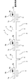
- FIG. 1 is a partial plan view schematically showing a configuration example of a main part of a solid-state imaging device according to Embodiment 1 of the present invention.
- the solid-state imaging device 1 of Embodiment 1 includes a plurality of light receiving elements 2 arranged in a matrix in the column direction (vertical direction) and the row direction (horizontal direction), and 4 ⁇ 2 ⁇ 2 rows.
- Each light receiving element 2 exposes each light receiving element 2 so as to allow light to enter, and a channel stop 4 (channel stop part) for preventing signal charges from entering between the adjacent upper, lower, left and right light receiving elements 2 ),
- Transfer electrodes 6a to 9a and transfer electrode wirings 6 to 9 for reading out charges and applying a charge transfer control signal for transferring charges in the vertical direction along the vertical transfer unit 5 are provided.
- the first row includes the transfer electrodes 7a and 9a (vertical transfer unit 5), the light receiving element 2, the channel stop 4, the light receiving element 2, and the transfer electrodes 7a and 9a (vertical transfer unit 5). ) Are repeated a plurality of times and arranged in this order in the row direction (lateral direction).
- the transfer electrodes 8a and 6a (vertical transfer unit 5), the light receiving element 2, the channel stop 4, the light receiving element 2, and the transfer electrodes 8a and 6a (vertical transfer unit 5) are repeated a plurality of times in the row direction (lateral direction). Are arranged in this order.
- the transfer electrode wirings 6 to 9 (transfer electrode wiring 8 is omitted here), the light receiving element 2, the channel stop 4, the light receiving element 2, and the transfer electrode wirings 6 to 9 are repeated a plurality of times in the column direction (vertical direction) in this order.
- the solid-state imaging device 1 of the first embodiment is a two-pixel shared CCD, and a plurality of light receiving elements 2 are respectively positioned in the column direction on both sides of each vertical transfer unit 5, and alternately from the light receiving elements 2 on both sides.
- the signal charge is read out to the vertical transfer unit 5 sandwiched between the light receiving elements 2 on both sides.
- the light receiving elements 2 in the same row are arranged adjacent to each other via the channel stop 4.
- the opening 3 is an opening region surrounded by the transfer electrode wirings 6 to 9 adjacent in the vertical direction and between the transfer electrodes 6a and 9a and the transfer electrodes 7a and 8a.
- Two rows of four light receiving elements 2 are arranged.
- Channel stops 4 are provided between the light receiving elements 2 in two columns and between the light receiving elements 2 in two rows, respectively.
- each light receiving element 2 is surrounded by a rectangular shape by the transfer electrode wirings 6 formed of the first polysilicon layer in the plan view and the transfer electrodes 6a to 9a.
- An opening 3 is formed.
- four light receiving elements 2 are provided by being partitioned by a cross-shaped channel stop 4.
- the channel stop 4 prevents signal charges from entering between pixels adjacent in the horizontal direction of the light receiving element 2 and prevents signal charges from entering between pixels adjacent to the light receiving element 2 in the vertical direction. ing. Between the four light receiving elements 2 of 2 columns ⁇ 2 rows, channel stops 4 are formed in a cross shape in plan view.
- the transfer electrode wiring 6 is made of a first-layer polysilicon layer, and is formed so as to extend in the horizontal direction between the light receiving elements 2 adjacent in the vertical transfer direction.
- a transfer electrode 6a extending in a comb shape (a right-angled triangular shape with a sharp tip) is provided on one side.
- the transfer electrode wiring 7 is formed of a second polysilicon layer formed on the transfer electrode wiring 6 via an interlayer insulating film, and extends horizontally between the light receiving elements 2 adjacent to each other in the vertical transfer direction.
- the transfer electrode 7a is formed on each vertical transfer portion 5 and extends downwardly (vertically in the other direction) in a comb-tooth shape (a right-angled triangular shape with a sharp tip).
- the transfer electrode wiring 8 is made of a third layer polysilicon layer or metal layer formed on the transfer electrode wiring 7 via an interlayer insulating film, and horizontally between the light receiving elements 2 adjacent to each other in the vertical transfer direction. It is formed so as to extend, and extends in a comb shape from the half-width portion on one side (here, the upper side in plan view) on each vertical transfer unit 5 to the upper side (one direction side along the vertical transfer direction) in plan view. It has a strip portion 8b. The strip portion 8b is electrically connected to a transfer electrode 8a having a triangular shape in a plan view via a contact plug 8c therebelow.
- the transfer electrode wiring 9 is made of a third-layer polysilicon layer or metal layer formed on the transfer electrode wiring 7 via an interlayer insulating film, and horizontally between the light receiving elements 2 adjacent to each other in the vertical transfer direction. It is formed so as to extend in a comb-like shape from the half-width portion on the other side (here, the lower side in plan view) on each vertical transfer portion 5 to the lower side in plan view (the other direction side along the vertical transfer direction)
- the strip portion 9b extends.
- the strip portion 9b is electrically connected to a transfer electrode 9a having a right triangle shape in plan view via a contact plug 9c (FIG. 2) below the strip portion 9b.
- Read drive is performed to alternately read out signal charges from the respective light receiving elements 2 in the left and right columns of the vertical transfer section 5 in which the triangular comb-tooth-shaped portions and the triangular island-shaped portions of the transfer electrodes 7a and 9a in the first row are located below. .
- Each transfer electrode 7a and 9a is partitioned by a rectangular diagonal line, and the hypotenuses of each triangle in plan view are opposed to each other, and the transfer electrodes 7a and 9a are insulated from each other. Reading of the signal charge from the light receiving element 2 to the vertical transfer unit 5 is performed through the side of each transfer electrode 7a, 9a facing the light receiving element 2 of each triangle in plan view.
- each transfer electrode 8a and 6a In the second row on the lower side of each transfer electrode 7a and 9a in plan view, the triangular island-like portion and the triangular comb-like portion of each transfer electrode 8a and 6a are received by the vertical transfer portion 5 below the respective light receiving columns.
- Read driving is performed to alternately read out signal charges from the element 2.
- Each transfer electrode 8a and 6a is partitioned by a rectangular diagonal line, and the hypotenuses of each triangle in plan view are opposed to each other, and each transfer electrode 8a and 6a is insulated from each other. Reading of the signal charge from the light receiving element 2 to the vertical transfer unit 5 is performed through the side of each transfer electrode 8a and 6a facing the light receiving element 2 of each triangle in plan view.
- FIG. 2 is a cross-sectional view taken along the line A1-A1 'of the solid-state image sensor 1 of FIG. 1
- FIG. 3 is a cross-sectional view taken along the line B1-B1' of the solid-state image sensor 1 of FIG.
- the solid-state imaging device 1 includes a plurality of light receiving elements 2 that generate signal charges by photoelectrically converting incident light on a semiconductor substrate.
- a transfer electrode 7a, 9a or transfer electrode 6a, 8a for controlling charge readout and charge transfer on the charge transfer part 5 for transferring the signal charge from the light receiving element 2 adjacent to 2
- the gate electrode is arranged.
- a light shielding film may be formed on the gate electrode to prevent incident light from being reflected by the gate electrode and generating noise.
- the transfer electrode wirings 6 to 9 and the transfer electrodes 6a to 9a are used as the light shielding film. It may be used.
- a microlens (not shown) for condensing light from the opening 3 through the interlayer insulating film 12 and a color filter (not shown) is disposed.
- An opening 3 serving as an opening region of an incident light window surrounded by the vertical transfer units 5 and 5 in the column direction is provided, and four light receiving elements 2 of 2 columns ⁇ 2 rows are provided in the opening 3.
- the signal charges are alternately read from the light receiving elements 2 in the same row arranged on both sides of the vertical transfer unit 5 and read out to the vertical transfer unit 5 adjacent thereto to be transferred.
- the wiring region in which the transfer electrode wiring extending in the row direction is removed between the light receiving elements 2 in the two rows on the upper side in the plan view and the light receiving elements 2 in the two rows on the lower side in the plan view is applied to the light receiving region.
- the number of pixels can be increased by further reducing the pixel size without reducing the light receiving sensitivity and dynamic range of the light receiving region.
- the light receiving sensitivity and dynamic range of the light receiving region can be further improved by maintaining the number of pixels and increasing the pixel size.
- an opening 3 as an opening area of an incident light window surrounded by the vertical transfer units 5 and 5 is provided, and each of the four light receiving elements 2 of 2 columns ⁇ 2 rows is arranged in the opening 3.
- transfer electrode wirings 6 to 11 and transfer electrode wirings 6 to 11 which will be described later in the row direction vertically adjacent to each other in the plan view intersect with each other at right angles to each other and in plan view.
- An opening 3A which will be described later, is provided as an opening region of an incident light window surrounded by the vertical transfer units 5 and 5 adjacent to each other in the adjacent column direction. A case where each light receiving element 2 is arranged will be described.
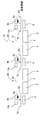
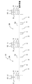
- FIG. 4 is a partial plan view schematically showing a configuration example of a main part of the solid-state imaging device according to Embodiment 2 of the present invention.
- the solid-state imaging device 1 ⁇ / b> A includes a plurality of light receiving elements 2 arranged in a matrix in the column direction (vertical direction) and the row direction (horizontal direction), and 6 ⁇ 2 ⁇ 3 rows.
- Transfer electrodes 6a to 9a and transfer electrode wirings 6 to 9 for applying a charge transfer control signal for transferring charges in the vertical direction along the vertical transfer unit 5 are provided.
- the first row includes the transfer electrodes 7a and 9a (vertical transfer unit 5), the light receiving device 2, the channel stop 4, the light receiving device 2, and the transfer electrodes 7a and 9a (vertical transfer unit 5). ) Are repeated a plurality of times and arranged in this order in the row direction (lateral direction).
- the transfer electrodes 11a and 10a (vertical transfer unit 5), the light receiving element 2, the channel stop 4, the light receiving element 2 and the transfer electrodes 11a and 10a (vertical transfer unit 5) are repeated a plurality of times in the row direction (lateral direction). Are arranged in this order.
- the transfer electrodes 8a and 6a (vertical transfer unit 5), the light receiving element 2, the channel stop 4, the light receiving element 2, and the transfer electrodes 8a and 6a (vertical transfer unit 5) are repeated a plurality of times in the row direction (lateral direction). Are arranged in this order. Also, transfer electrode wirings 6 to 11 (transfer electrode wirings 8 and 10 are omitted here), light receiving element 2, channel stop 4, light receiving element 2, channel stop 4, light receiving element 2, and transfer electrode wirings 6 to 11 are repeated a plurality of times. Are arranged in this order in the column direction (vertical direction).
- the solid-state imaging device 1A of the second embodiment is a two-pixel shared CCD, and a plurality of light receiving elements 2 are respectively positioned in the column direction on both sides of each vertical transfer unit 5, and alternately from the light receiving elements 2 on both sides.
- the signal charge is read out to the vertical transfer unit 5 sandwiched between the light receiving elements 2 on both sides.
- the light receiving elements 2 in the same row are arranged adjacent to each other via the channel stop 4.
- the opening 3A is an opening surrounded by the upper and lower adjacent transfer electrode wirings 6 to 11 and the transfer electrode wirings 6 to 11 and between the transfer electrodes 6a, 9a and 10a and the transfer electrodes 7a, 8a and 11a.
- the six light receiving elements 2 of 2 columns ⁇ 3 rows are arranged in this opening area.
- Channel stops 4 are respectively provided between the light receiving elements 2 in two rows and between the light receiving elements 2 in the plan view.
- each light receiving element 2 is surrounded by a rectangular shape by the transfer electrode wirings 6 formed of the first polysilicon layer in the plan view and the transfer electrodes 6a to 11a.
- An opening 3A is formed. In the region of the opening 3A, six light receiving elements 2 are provided by being partitioned by two cross-shaped channel stops 4 in the plan view.
- the channel stop 4 prevents signal charges from entering between pixels adjacent in the horizontal direction of the light receiving element 2 and prevents signal charges from entering between pixels adjacent to the light receiving element 2 in the vertical direction. ing. Between the six light receiving elements 2 of 2 columns ⁇ 3 rows, channel stops 4 are formed in two cross shapes in the upper and lower sides in plan view.
- the transfer electrode wiring 6 is made of a first-layer polysilicon layer, and is formed so as to extend in the horizontal direction between the light receiving elements 2 adjacent in the vertical transfer direction.
- a transfer electrode 6a extending in a comb shape (a right-angled triangular shape with a sharp tip) is provided on one side.
- the transfer electrode wiring 7 is formed of a second polysilicon layer formed on the transfer electrode wiring 6 via an interlayer insulating film, and extends horizontally between the light receiving elements 2 adjacent to each other in the vertical transfer direction.
- the transfer electrode 7a is formed on each vertical transfer portion 5 and extends downwardly (vertically in the other direction) in a comb-tooth shape (a right-angled triangular shape with a sharp tip).
- the transfer electrode wiring 8 is made of a third layer polysilicon layer or metal layer formed on the transfer electrode wiring 7 via an interlayer insulating film, and horizontally between the light receiving elements 2 adjacent to each other in the vertical transfer direction. It is formed so as to extend, and extends in a comb shape from the half-width portion on one side (here, the upper side in plan view) on each vertical transfer unit 5 to the upper side (one direction side along the vertical transfer direction) in plan view. It has a strip portion 8b. The strip portion 8b is electrically connected to a transfer electrode 8a having a triangular shape in a plan view via a contact plug 8c therebelow.
- the transfer electrode wiring 9 is made of a third-layer polysilicon layer or metal layer formed on the transfer electrode wiring 7 via an interlayer insulating film, and horizontally between the light receiving elements 2 adjacent to each other in the vertical transfer direction. It is formed so as to extend in a comb-like shape from the half-width portion on the other side (here, the lower side in plan view) on each vertical transfer portion 5 to the lower side in plan view (the other direction side along the vertical transfer direction)
- the strip portion 9b extends.
- the strip portion 9b is electrically connected to a transfer electrode 9a having a triangular shape in a plan view via a contact plug 9c (FIG. 5) therebelow.
- the transfer electrode wiring 10 is composed of a fourth polysilicon layer or metal layer formed on the transfer electrode wiring 8 via an interlayer insulating film, and horizontally between the light receiving elements 2 adjacent to each other in the vertical transfer direction. It is formed so as to extend, and extends in a comb shape from the half-width portion on one side (here, the upper side in plan view) on each vertical transfer unit 5 to the upper side (one direction side along the vertical transfer direction) in plan view. It has a strip portion 10b. The strip portion 10b is electrically connected to a transfer electrode 10a having a right triangle shape in plan view via a contact plug 10c therebelow.
- the transfer electrode wiring 11 is composed of a fourth polysilicon layer or metal layer formed on the transfer electrode wiring 9 via an interlayer insulating film, and horizontally between the light receiving elements 2 adjacent to each other in the vertical transfer direction. It is formed so as to extend in a comb-like shape from the half-width portion on the other side (here, the lower side in plan view) on each vertical transfer portion 5 to the lower side in plan view (the other direction side along the vertical transfer direction)
- the strip portion 11b extends.
- the strip portion 11b is electrically connected to a transfer electrode 11a having a triangular shape in a plan view via a contact plug 11c therebelow.
- Read drive is performed to alternately read out signal charges from the respective light receiving elements 2 in the left and right columns of the vertical transfer section 5 in which the triangular comb-tooth-shaped portions and the triangular island-shaped portions of the transfer electrodes 7a and 9a in the first row are located below. .
- Each transfer electrode 7a and 9a is partitioned by a rectangular diagonal line, and the hypotenuses of each triangle in plan view are opposed to each other, and the transfer electrodes 7a and 9a are insulated from each other. Reading of the signal charge from the light receiving element 2 to the vertical transfer unit 5 is performed through the side of each transfer electrode 7a, 9a facing the light receiving element 2 of each triangle in plan view.
- each triangular island-like portion of each transfer electrode 11a and 10a is alternately transferred from the respective light receiving elements 2 in the left and right columns to the vertical transfer section 5 below.
- Read drive for reading signal charges is performed.
- Each transfer electrode 11a and 10a is partitioned by a rectangular diagonal line, and the hypotenuses of each triangle in plan view are opposed to each other, and each transfer electrode 11a and 10a is insulated from each other. Reading of the signal charge from the light receiving element 2 to the vertical transfer unit 5 is performed through the side of each transfer electrode 11a and 10a facing the light receiving element 2 of each triangle in plan view.
- each of the left and right columns is received by the vertical transfer unit 5 under which the triangular island-like portion and the triangular comb-like portion of each transfer electrode 8a and 6a are located.
- Read driving is performed to alternately read out signal charges from the element 2.
- Each transfer electrode 8a and 6a is partitioned by a rectangular diagonal line, and the hypotenuses of each triangle in plan view are opposed to each other, and each transfer electrode 8a and 6a is insulated from each other. Reading of the signal charge from the light receiving element 2 to the vertical transfer unit 5 is performed through the side of each transfer electrode 8a and 6a facing the light receiving element 2 of each triangle in plan view.
- FIG. 5 is a cross-sectional view taken along the line A2-A2 'of the solid-state imaging device 1A shown in FIG. 4
- FIG. 6 is a cross-sectional view taken along the line B2-B2' of the solid-state imaging device 1A shown in FIG.
- the solid-state imaging device 1A includes a plurality of light receiving elements 2 that photoelectrically convert incident light to generate signal charges on a semiconductor substrate, and each light receiving element. Adjacent to 2, a charge transfer portion 5 for transferring signal charges from the light receiving element 2 and transfer electrodes 7 a and 9 a or transfer electrodes 6 a and 8 a for controlling charge reading and charge transfer thereon. Gate electrodes as transfer electrodes 11a and 10a are arranged. A light shielding film may be formed on the gate electrode to prevent incident light from being reflected by the gate electrode and generating noise. The transfer electrode wirings 6 to 11 and the transfer electrodes 6a to 11a are used as the light shielding film. It may be used.
- a microlens (not shown) for condensing light to each light receiving element 2 from the opening 3A through the interlayer insulating film 12 and a color filter (not shown) is arranged.
- An opening 3A as an opening region of an incident light window surrounded by the vertical transfer units 5 and 5 in the column direction adjacent to each other in view is provided, and each of six light receiving elements of 2 columns ⁇ 3 rows in the opening 3A.
- the device 2 is arranged, and signal charges are alternately read out from the respective light receiving elements 2 in the same row arranged on both sides of the vertical transfer unit 5 to the adjacent vertical transfer unit 5 so as to be transferred in the vertical direction. It has become.
- each light receiving element 2 is maintained in a state in which the light receiving area of each light receiving element 2 is maintained by applying a wiring area to which the transfer electrode wiring extending in the row direction is removed from each light receiving element 2 in the column to the light receiving area.
- the pixel size can be further reduced to further increase the number of pixels.
- the number of pixels can be maintained and the pixel size can be increased to improve the light receiving sensitivity and dynamic range of the light receiving region.
- the effect of the second embodiment is greater than that of the first embodiment, but the substrate becomes thicker.
- the transfer electrode wirings 6 to 9 have three layers, and the first-layer transfer electrode wiring 6 has a right-angled triangular shape with an acute tip on the upper side in plan view on the vertical transfer portion 5.
- the second-layer transfer electrode wiring 7 has a right-angled triangular shape with a sharp tip at the lower side in plan view on the vertical transfer portion 5.
- the third-layer transfer electrode wiring 8 that has a comb-like transfer electrode 7a (second transfer electrode) that extends and is half in width and located on the upper side in plan view is comb-shaped on the upper side in plan view on the vertical transfer unit 5.
- the comb-like portion is electrically connected to the transfer electrode 8a (third transfer electrode) having a triangular shape in a plan view via the contact plug 8c thereunder, and has a width extending in a tooth shape.
- the transfer electrode wiring 9 of the third layer located in the lower half of the plan view is in a comb-like shape on the vertical transfer unit 5 on the lower side of the plan view.
- the comb-like portion is electrically connected to the transfer electrode 9a (fourth transfer electrode) having a right triangle shape in plan view via the contact plug 9c therebelow.
- the signal charges are read out from the light receiving element 2 adjacent to the vertical transfer part 5 through the sides of the right-angled triangles of the transfer electrode 7a and the transfer electrode 9a, and the second line is transferred to the transfer electrode 6a.
- the signal charges are read out from the light receiving elements adjacent to the vertical transfer section 5 through the sides of the right-angled triangles of the electrode 8a in plan view.
- the transfer electrode wirings 6 to 11 are four layers, and the first-layer transfer electrode wiring 6 has a right-angled triangular shape with an acute tip on the upper side in plan view on the vertical transfer portion 5.
- the second-layer transfer electrode wiring 7 has a right-angled triangular shape with a sharp tip at the lower side in plan view on the vertical transfer portion 5.
- the third-layer transfer electrode wiring 8 having a comb-like transfer electrode 7a (second transfer electrode) extending and having a half width and positioned on the upper side in plan view is comb-shaped above the vertical transfer unit 5 and on the upper side in plan view.
- the comb-like portion is electrically connected to the transfer electrode 8a (third transfer electrode) having a right-angled triangular shape in plan view via the contact plug 8c thereunder, and has a width.
- the third-layer transfer electrode wiring 9 that is located in the lower half of the plan view in a half is comb-like on the vertical transfer portion 5 on the lower side of the plan view.
- This comb-like portion is electrically connected to the transfer electrode 9a (fourth transfer electrode) having a right triangle shape in plan view via the contact plug 9c below it, and has a half width and a flat surface.
- the transfer electrode wiring 10 in the fifth layer on the upper side of the view has a portion extending in a comb shape above the vertical transfer portion 5 and on the upper side in the plan view, and this comb-like portion is interposed via the contact plug 10 c therebelow.
- the fourth-layer transfer electrode wiring 11 that is electrically connected to the transfer electrode 10a (fifth transfer electrode) having a right triangle island shape in plan view and having a half width and located on the lower side in plan view is above the vertical transfer unit 5 And has a portion extending in a comb-like shape on the lower side in plan view, and this comb-like portion is electrically connected to a transfer electrode 11a (sixth transfer electrode) having a right-angled triangular island shape in plan view via a contact plug 11c therebelow.
- each of the transfer electrode 7a and the transfer electrode 9a The signal charges are read from the light receiving elements adjacent to the vertical transfer portion 5 through the side portions of the right-angled triangle in plan view, and the second row shows the side portions of the right-angled triangles in the plan view of the transfer electrode 10a and the transfer electrode 11a.
- the signal charges are read out from the light receiving element 2 adjacent to the vertical transfer unit 5 through the vertical transfer unit 5, and the third row is vertically transferred through the side portions of the right-angled triangles of the transfer electrode 6a and the transfer electrode 8a.
- the signal charge is read out from the light receiving element 2 adjacent to the unit 5.
- An opening 3 is provided as an opening region of the incident light window surrounded by the vertical transfer units 5 and 5 in the column direction.
- Four light receiving elements 2 of 2 columns ⁇ 2 rows are provided in the opening 3.
- the row of transfer electrode wirings 6 to 11 and the transfer electrode wirings 6 to 11 adjacent to each other in the vertical direction in a plan view intersect with each other at a right angle and are adjacent to each other in a plan view.
- An opening 3A is provided as an opening area of the incident light window surrounded by the vertical transfer units 5 and 5 in the direction, and six light receiving elements 2 of 2 columns ⁇ 3 rows are arranged in the opening 3A. ing.
- the present invention is applied to the case where an opening as an opening region of the incident light window is provided, and 2 ⁇ n light receiving elements 2 of 2 columns ⁇ n rows (n is a plurality) are arranged in the opening. be able to.
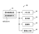
- FIG. 7 is a block diagram illustrating a schematic configuration example of an electronic information device using any of the solid-state imaging devices according to the first and second embodiments of the present invention as an imaging unit as the third embodiment of the present invention.
- the electronic information device 90 performs predetermined signal processing (noise removal processing, black level processing) on the imaging signal obtained by amplifying the signal charge from the solid-state imaging device 1 or 1A according to the first and second embodiments. , White balance, color interpolation processing, ⁇ processing, etc.) to obtain a color image signal, and data after performing predetermined signal processing for recording the color image signal from the solid-state imaging device 91
- a memory unit 92 such as a recording medium that can be recorded, and a liquid crystal display device that can display a color image signal from the solid-state imaging device 91 on a display screen such as a liquid crystal display screen after performing predetermined signal processing for display Display unit 93 and a communication unit 94 such as a transmission / reception device that can perform communication processing after performing predetermined signal processing for color image signals from the solid-state imaging device 91 for communication.
- an image output unit 95 such as a printer which allows printing the color image signal from the solid-state imaging device 91 after a predetermined printing signal processing for printing.
- the electronic information device 90 is not limited to this, but in addition to the solid-state imaging device 91, at least one of a memory unit 92, a display unit 93, a communication unit 94, and an image output unit 95 such as a printer. You may have.
- the electronic information device 90 includes, for example, a digital camera such as a digital video camera and a digital still camera, an in-vehicle camera such as a surveillance camera, a door phone camera, and an in-vehicle rear surveillance camera, and a video phone camera.
- a digital camera such as a digital video camera and a digital still camera
- an in-vehicle camera such as a surveillance camera, a door phone camera, and an in-vehicle rear surveillance camera
- a video phone camera includes, for example, a digital camera such as a digital video camera and a digital still camera
- an in-vehicle camera such as a surveillance camera, a door phone camera, and an in-vehicle rear surveillance camera
- a video phone camera such as an image input camera, a scanner device, a facsimile device, a camera-equipped mobile phone device, and a portable terminal device (PDA) is conceivable.
- PDA portable terminal device
- the third embodiment based on the color image signal from the solid-state imaging device 91, it can be displayed on the display screen, or can be printed out on the paper by the image output unit 95. (Printing), communicating this as communication data in a wired or wireless manner, performing a predetermined data compression process in the memory unit 92 and storing it in a good manner, or performing various data processings satisfactorily Can do.
- Print communicating this as communication data in a wired or wireless manner, performing a predetermined data compression process in the memory unit 92 and storing it in a good manner, or performing various data processings satisfactorily Can do.
- the present invention relates to a solid-state imaging device provided with a plurality of light-receiving units that photoelectrically convert image light from a subject and to image, and a digital video camera and a digital still, for example, using the solid-state imaging device as an image input device in an imaging unit
- a solid-state imaging device provided with a plurality of light-receiving units that photoelectrically convert image light from a subject and to image
- a digital video camera and a digital still for example, using the solid-state imaging device as an image input device in an imaging unit
- image input cameras such as surveillance cameras, scanner devices, facsimile devices, television telephone devices, and mobile phone devices with cameras
- light receiving areas are further reduced in the wiring area.
- the number of pixels can be increased by further reducing the pixel size without reducing the light receiving sensitivity and dynamic range of the light receiving region while maintaining the light receiving area of each light receiving element.
Landscapes
- Solid State Image Pick-Up Elements (AREA)
- Transforming Light Signals Into Electric Signals (AREA)
Abstract
配線領域を更に低減した領域を受光領域に当てることにより、各受光素子の受光面積を維持した状態で、受光領域の受光感度やダイナミックレンジの低減を招くことなく、更なる画素サイズの縮小を行って画素数を増加させる。 平面視で上下に隣接する行方向の転送電極配線6~9と転送電極配線6~9との間および、これらに直角に交差し、平面視で隣接する列方向の各垂直転送部5,5間で囲まれた入射光窓の開口領域としての開口部3が設けられ、開口部3内に2列×2行の4個の各受光素子2が配置され、垂直転送部5の両側に配列された同じ行の各受光素子2から交互に信号電荷がこれに隣接の垂直転送部5に読み出されて電荷転送される。
Description
本発明は、被写体からの画像光を光電変換して撮像する複数の受光部が設けられた固体撮像素子および、この固体撮像素子を画像入力デバイスとして撮像部に用いた例えばデジタルビデオカメラおよびデジタルスチルカメラなどのデジタルカメラや、監視カメラなどの画像入力カメラ、スキャナ装置、ファクシミリ装置、テレビジョン電話装置、カメラ付き携帯電話装置などの電子情報機器に関する。
この種の従来の固体撮像素子は、2画素共有CCD固体撮像素子であり、信号電荷を電荷転送する垂直転送部の両側に垂直列の複数の各受光素子が左右に配置している。このように、2列の複数画素に対して1本の垂直転送部が設けられた構成が行方向に繰り返し配列されている。これは、1列の複数画素に対して1本の垂直転送部が設けられる場合に比べて、2列の複数画素に対して1本の垂直転送部の単位で、垂直転送部が1本少なくなる。このため、各受光素子の受光面積を増大させることができるかまたは、各受光素子の受光面積を維持した状態で受光感度やダイナミックレンジを低減させずに、画素サイズを縮小して画素数を増加させている。
図8は、特許文献1に開示されている従来の固体撮像素子の要部構成例を模式的に示す一部平面図である。
図8において、従来の固体撮像素子100は、列方向および行方向にマトリクス状に配設された複数の受光素子101と、各受光素子101上を露出させて光を入れる開口部102と、受光素子101の水平転送方向に隣接する各画素間の信号電荷の侵入を防止するためのチャンネルストップ103と、両側に位置する垂直列の複数の各受光素子101からの信号電荷を読み出して垂直転送方向に転送するための垂直転送部104と、垂直転送部104に受光素子101の信号電荷を読み出して、垂直転送部104に沿って垂直方向(列方向)に信号電荷を電荷転送するための電荷転送制御信号を印加するための転送電極105~107とを有している。
従来の固体撮像素子100において、転送電極107,106(垂直転送部104)、受光素子101、チャンネルストップ103、受光素子101および転送電極107,106(垂直転送部104)を行方向(横方向)にこの順に配列している。また、転送電極105、受光素子101、転送電極105~107、受光素子101および転送電極105~107を列方向(縦方向)にこの順に配列している。各垂直転送部104の両側には、列方向に複数の受光素子101がそれぞれ位置され、両側の受光素子101から交互に、真ん中の垂直転送部104に信号電荷が読み出される。また、同じ行の受光素子101がチャンネルストップ103を介して互いに隣接している。
転送電極105は、第1層目のポリシリコンからなり、垂直転送方向に隣接する受光素子101間上を水平転送方向に延びるように形成され、各垂直転送部104上において下側(垂直転送方向に沿って一方の側)に櫛歯状に延びる部分を有している。
転送電極106は、第2層目のポリシリコンからなり、垂直転送方向に隣接する受光素子101間上を水平転送方向に延びるように形成され、各垂直転送部104上における一方の側(ここでは右側)の半部幅において上側(垂直転送方向に沿って他方の側)に櫛歯状に延びる部分を有する。
転送電極107は、第3層目のポリシリコンからなり、垂直転送方向に隣接する受光素子101間上を水平転送方向に延びるように形成され、各垂直転送部104上における他方の側(ここでは左側)の半部幅において上側(垂直転送方向に沿って他方の側)に櫛歯状に延びる部分を有する。
上から視ると、各受光素子101は、第1層目のポリシリコンからなる転送電極105と、第2層目のポリシリコンからなる転送電極106と、第3層目のポリシリコンからなる転送電極107により囲まれて開口部102を構成している。各転送電極106の各櫛歯状部分がその下にある垂直転送部104へその右側の受光素子101から信号電荷を読み出す読み出し駆動をする部分となっている。また、各転送電極107の各櫛歯状部分がその下にある垂直転送部104へその左側の受光素子101から信号電荷を読み出す読み出し駆動をする部分となっている。
特許文献2では、上記特許文献1の構成と同様に、従来の固体撮像素子は、列方向および行方向にマトリクス状に配設された複数の受光素子が配列されている。垂直転送部の両側に垂直列の複数の各受光素子が配置されている構成となっている。この構成が行方向に繰り返されている。両側の受光素子からの信号電荷が交互に、その間の垂直転送部に読み出されて垂直転送部に沿って垂直方向に電荷転送される。
上記特許文献1、2にそれぞれ開示されている従来の構成では、列方向および行方向にマトリクス状に複数の受光素子が配列されているが、更なる受光素子のセルサイズの縮小を行って画素数を増加させる場合には、受光感度やダイナミックレンジの低下を招いてしまうという問題を有していた。
本発明は、上記従来の問題を解決するもので、配線領域を更に低減した領域を受光領域に当てることにより、各受光素子の受光面積を維持した状態で、受光領域の受光感度やダイナミックレンジの低減を招くことなく、更なる画素サイズの縮小を行って画素数を増加させることができる固体撮像素子および、この固体撮像素子を画像入力デバイスとして撮像部に用いた例えばカメラ付き携帯電話装置などの電子情報機器を提供することを目的とする。
本発明の固体撮像素子は、信号電荷を電荷転送する垂直転送部の両側に垂直列の複数の受光素子がそれぞれ配列されている構成が複数繰り返された2画素共有構成の固体撮像素子において、平面視で隣接する各転送電極配線間と、これに直交し、平面視で隣接する各垂直転送部間で囲まれた入射光用の開口領域が設けられ、該開口領域内に2列×n行(nは複数)の2×n個の各受光素子が配置され、該垂直転送部の両側に配列された同行の各受光素子から交互に信号電荷が当該垂直転送部に読み込まれて電荷転送されるものであり、そのことにより上記目的が達成される。
また、好ましくは、本発明の固体撮像素子における2列×n行(nは複数)の2×n個の各受光素子は、2列×2行の4個の各受光素子または2列×3行の6個の各受光素子である。
さらに、好ましくは、本発明の固体撮像素子における開口領域内の前記受光素子の互いに隣接する上下左右間で信号電荷の侵入を防止するためのチャンネルストップ部が半導体基板上部の該受光素子の間に設けられている。
さらに、好ましくは、本発明の固体撮像素子における垂直転送部に前記受光素子から信号電荷を読み出して、該垂直転送部に沿って垂直方向に電荷転送させるための電荷転送制御信号を印加する複数の転送電極およびこれらにそれぞれ接続された複数の転送電極配線が設けられている。即ち、前記垂直転送部に前記受光素子から信号電荷を読み出して、該垂直転送部に沿って垂直方向に電荷転送させるための電荷転送制御信号が印加される複数の転送電極が、前記転送電極配線間の該垂直転送部上に設けられ、前記各転送電極配線がそれぞれ該複数の転送電極にそれぞれ電気的に接続されている。
さらに、好ましくは、本発明の固体撮像素子における2列×n行(nは複数)の2×n個の各受光素子が、2列×2行の4個の各受光素子の場合に、前記転送電極配線は3層であり、第1層目の転送電極配線は、前記垂直転送部上で平面視上側に、先端が鋭角の直角三角形状に延びる櫛歯状の第1転送電極を有し、第2層目の転送電極配線は、該垂直転送部上で平面視下側に、先端が鋭角の直角三角形状に延びる櫛歯状の第2転送電極を有し、半幅で平面視上側の第3層目の転送電極配線は、該垂直転送部上で平面視上側に櫛歯状に延びる部分を有し、該櫛歯状の部分がその下のコンタクトプラグを介して平面視直角三角形島状の第3転送電極に電気的に接続され、半幅で平面視下側の第3層目の転送電極配線は、該垂直転送部上で平面視下側に櫛歯状に延びる部分を有し、該櫛歯状の部分がその下のコンタクトプラグを介して平面視直角三角形島状の第4転送電極に電気的に接続されており、1行目は該第2転送電極と該第4転送電極の各平面視直角三角形の辺部分をそれぞれ通して該垂直転送部にこれに隣接する受光素子から信号電荷が読み出され、2行目は該第1転送電極と該第3転送電極の各平面視直角三角形の辺部分をそれぞれ通して該垂直転送部にこれに隣接する受光素子から信号電荷が読み出される。
さらに、好ましくは、本発明の固体撮像素子における2列×n行(nは複数)の2×n個の各受光素子が、2列×3行の6個の各受光素子の場合に、前記転送電極配線は4層であり、第1層目の転送電極配線は、前記垂直転送部上で平面視上側に、先端が鋭角の直角三角形状に延びる櫛歯状の第1転送電極を有し、第2層目の転送電極配線は、該垂直転送部上で平面視下側に、先端が鋭角の直角三角形状に延びる櫛歯状の第2転送電極を有し、半幅で平面視上側の第3層目の転送電極配線は、該垂直転送部上で平面視上側に櫛歯状に延びる部分を有し、該櫛歯状の部分がその下のコンタクトプラグを介して平面視直角三角形島状の第3転送電極に電気的に接続され、半幅で平面視下側の第3層目の転送電極配線は、該垂直転送部上で平面視下側に櫛歯状に延びる部分を有し、該櫛歯状の部分がその下のコンタクトプラグを介して平面視直角三角形島状の第4転送電極に電気的に接続され、半幅で平面視上側の第4層目の転送電極配線は、該垂直転送部上で平面視上側に櫛歯状に延びる部分を有し、該櫛歯状の部分がその下のコンタクトプラグを介して平面視直角三角形島状の第5転送電極に電気的に接続され、半幅で平面視下側の第4層目の転送電極配線は、該垂直転送部上で平面視下側に櫛歯状に延びる部分を有し、該櫛歯状の部分がその下のコンタクトプラグを介して平面視直角三角形島状の第6転送電極に電気的に接続されており、1行目は該第2転送電極と該第4転送電極の各平面視直角三角形の辺部分をそれぞれ通して該垂直転送部にこれに隣接する受光素子から信号電荷が読み出され、2行目は該第5転送電極と該第6転送電極の各平面視直角三角形の辺部分をそれぞれ通して該垂直転送部にこれに隣接する受光素子から信号電荷が読み出され、3行目は該第1転送電極と該第3転送電極の各平面視直角三角形の辺部分をそれぞれ通して該垂直転送部にこれに隣接する受光素子から信号電荷が読み出される。
本発明の電子情報機器は、本発明の上記固体撮像素子を画像入力デバイスとして撮像部に用いたものであり、そのことにより上記目的が達成される。
上記構成により、以下、本発明の作用を説明する。
本発明においては、平面視で隣接する各転送電極配線間と、これに直交し、平面視で隣接する各垂直転送部間で囲まれた入射光用の開口領域が設けられ、この開口領域内に2列×n行(nは複数)の2×n個の各受光素子が配置され、垂直転送部の両側に配列された同行の各受光素子から交互に信号電荷が当該垂直転送部に読み込まれて電荷転送される。
これによって、各受光素子の受光面積を維持した状態で、配線領域を更に低減した領域を受光領域に当てることにより、受光領域の受光感度やダイナミックレンジの低減を招くことなく、更なる画素サイズの縮小を行うことが可能となる。
以上により、本発明によれば、配線領域を更に低減した領域を受光領域に当てることにより、各受光素子の受光面積を維持した状態で、受光領域の受光感度やダイナミックレンジの低減を招くことなく、更なる画素サイズの縮小を行うことができる。
1、1A 固体撮像素子
2 受光素子
3、3A 開口部
4 チャンネルストップ
5 垂直転送部(垂直転送レジスタ)
6~11 転送電極配線
6a~11a 転送電極
9c~11c コンタクトプラグ
12 層間絶縁膜
90 電子情報機器
91 固体撮像装置
92 メモリ部
93 表示部
94 通信部
95 画像出力部
2 受光素子
3、3A 開口部
4 チャンネルストップ
5 垂直転送部(垂直転送レジスタ)
6~11 転送電極配線
6a~11a 転送電極
9c~11c コンタクトプラグ
12 層間絶縁膜
90 電子情報機器
91 固体撮像装置
92 メモリ部
93 表示部
94 通信部
95 画像出力部
以下に、本発明の固体撮像素子の実施形態1、2および、この固体撮像素子の実施形態1、2のいずれかを画像入力デバイスとして撮像部に用いた例えばカメラ付き携帯電話装置などの電子情報機器の実施形態3について図面を参照しながら詳細に説明する。なお、各図における構成部材のそれぞれの厚みや長さなどは図面作成上の観点から、図示する構成に限定されるものではない。
(実施形態1)
図1は、本発明の実施形態1における固体撮像素子の要部構成例を模式的に示す一部平面図である。
図1は、本発明の実施形態1における固体撮像素子の要部構成例を模式的に示す一部平面図である。
図1において、本実施形態1の固体撮像素子1は、列方向(縦方向)および行方向(横方向)にマトリクス状に配設された複数の受光素子2と、2列×2行の4個の受光素子2毎に各受光素子2上を露出させて光を入れる開口部3と、隣接する上下左右の受光素子2間で信号電荷の侵入を防止するためのチャンネルストップ4(チャンネルストップ部)と、両側に位置する垂直列の複数の各受光素子2からの信号電荷を読み出して垂直転送方向に転送するための複数の垂直転送部5と、垂直転送部5に受光素子2からの信号電荷を読み出して、垂直転送部5に沿って垂直方向に電荷転送するための電荷転送制御信号を印加するための転送電極6a~9aおよび転送電極配線6~9とを有している。
本実施形態1の固体撮像素子1において、1行目は、転送電極7a、9a(垂直転送部5)、受光素子2、チャンネルストップ4、受光素子2および転送電極7a,9a(垂直転送部5)を複数繰り返して行方向(横方向)にこの順に配列している。2行目は、転送電極8a、6a(垂直転送部5)、受光素子2、チャンネルストップ4、受光素子2および転送電極8a,6a(垂直転送部5)を複数繰り返して行方向(横方向)にこの順に配列している。また、転送電極配線6~9(転送電極配線8はここでは省略)、受光素子2、チャンネルストップ4、受光素子2、転送電極配線6~9を複数繰り返して列方向(縦方向)にこの順に配列している。本実施形態1の固体撮像素子1は、2画素共有CCDであり、各垂直転送部5の両側には、列方向に複数の受光素子2がそれぞれ位置され、両側の受光素子2から交互に、両側の受光素子2に挟まれた垂直転送部5に信号電荷が読み出されるようになっている。また、同じ行の受光素子2がチャンネルストップ4を介して互いに隣接配置されている。
開口部3は、上下に隣接する転送電極配線6~9間と、転送電極6a,9aと転送電極7a,8aとの間で囲まれた開口領域であって、この開口領域内に2列×2行の4個の受光素子2が配置されている。2列の各受光素子2間および2行の各受光素子2間にはそれぞれチャンネルストップ4が設けられている。要するに、平面視において、各受光素子2は、第1層目のポリシリコン層からなる平面視上下の転送電極配線6と、転送電極6a~9aとにより4角形状に囲まれて入射光窓の開口部3を形成している。この開口部3の領域に4つの受光素子2が十字状のチャンネルストップ4で仕切られて設けられている。
チャンネルストップ4は、受光素子2の水平方向に隣接する各画素間の信号電荷の侵入を防止すると共に、受光素子2の垂直方向に隣接する各画素間の信号電荷の侵入を防止するようになっている。2列×2行の4個の各受光素子2間には、チャンネルストップ4が平面視で十字状に形成されている。
転送電極配線6は、第1層目のポリシリコン層からなり、垂直転送方向に隣接する受光素子2間上を水平方向に延びるように形成されており、各垂直転送部5上において上側(垂直一方向側)に櫛歯状(先端が鋭角の直角三角形状)に延びる転送電極6aを有している。
転送電極配線7は、転送電極配線6上に層間絶縁膜を介して形成された第2層目のポリシリコン層からなり、垂直転送方向に隣接する受光素子2間上を水平方向に延びるように形成されており、各垂直転送部5上において下側(垂直他方向側)に櫛歯状(先端が鋭角の直角三角形状)に延びる転送電極7aを有している。
転送電極配線8は、転送電極配線7上に層間絶縁膜を介して形成された第3層目のポリシリコン層または金属層からなり、垂直転送方向に隣接する受光素子2間上を水平方向に延びるように形成されており、各垂直転送部5上における一方の側(ここでは平面視で上側)の半幅部から平面視上側(垂直転送方向に沿って一方向側)に櫛歯状に延びる短冊部分8bを有している。この短冊部分8bは、その下のコンタクトプラグ8cを介して平面視直角三角形状の転送電極8aに電気的に接続されている。
転送電極配線9は、転送電極配線7上に層間絶縁膜を介して形成された第3層目のポリシリコン層または金属層からなり、垂直転送方向に隣接する受光素子2間上を水平方向に延びるように形成されており、各垂直転送部5上における他方の側(ここでは平面視下側)の半幅部から平面視下側(垂直転送方向に沿って他方向側)に櫛歯状に延びる短冊部分9bを有している。この短冊部分9bは、その下のコンタクトプラグ9c(図2)を介して平面視直角三角形状の転送電極9aに電気的に接続されている。
1行目の各転送電極7aおよび9aの三角形櫛歯状部分および三角形島状部分がその下にある垂直転送部5にその左右列の各受光素子2から交互に信号電荷を読み出す読み出し駆動をする。各転送電極7aおよび9aは4角形の対角線で仕切られて平面視各三角形の斜辺部分が互いに対向して、各転送電極7a、9aが互いに絶縁されている。受光素子2から垂直転送部5への信号電荷の読み出しは、各転送電極7a、9aの平面視各三角形の受光素子2に対向した辺側を通して行われる。
各転送電極7aおよび9aの平面視下側の2行目において、各転送電極8aおよび6aの三角形島状部分および三角形櫛歯状部分がその下にある垂直転送部5にその左右列の各受光素子2から交互に信号電荷を読み出す読み出し駆動をする。各転送電極8aおよび6aは4角形の対角線で仕切られて平面視各三角形の斜辺部分が互いに対向して、各転送電極8aおよび6aが互いに絶縁されている。受光素子2から垂直転送部5への信号電荷の読み出しは、各転送電極8aおよび6aの平面視各三角形の受光素子2に対向した辺側を通して行われる。
図2は、図1の固体撮像素子1におけるA1-A1’線断面図であり、図3は、図1の固体撮像素子1におけるB1-B1’線断面図である。
図2および図3において、本実施形態1の固体撮像素子1は、半導体基板上に、入射光を光電変換して信号電荷を生成する複数の受光素子2がマトリクス状に設けられ、各受光素子2に隣接して受光素子2からの信号電荷を電荷転送するための電荷転送部5およびこの上にこれを電荷読み出しおよび電荷転送を制御するための転送電極7a、9aまたは転送電極6a、8aとしてのゲート電極が配置されている。このゲート電極上には、入射光がゲート電極により反射してノイズが発生するのを防ぐために遮光膜が形成されていてもよく、転送電極配線6~9および転送電極6a~9aを遮光膜として用いてもよい。
また、受光素子2の上方には、開口部3から層間絶縁膜12および図示しないカラーフィルタを介して、受光素子2に光を集光させるための図示しないマイクロレンズが配置されている。
以上により、本実施形態1によれば、平面視で上下に隣接する行方向の転送電極配線6~9と転送電極配線6~9との間および、これらに直角に交差し、平面視で隣接する列方向の各垂直転送部5,5間で囲まれた入射光窓の開口領域としての開口部3が設けられ、開口部3内に2列×2行の4個の各受光素子2が配置され、垂直転送部5の両側に配列された同じ行の各受光素子2から交互に信号電荷がこれに隣接の垂直転送部5に読み出されて電荷転送されるようになっている。
このように、平面視上側の2列の各受光素子2と、平面視下側の2列の各受光素子2との間に行方向に延びる転送電極配線を取り除いた配線領域を受光領域に当てることにより、各受光素子2の受光面積を維持した状態で、受光領域の受光感度やダイナミックレンジの低減を招くことなく、更なる画素サイズの縮小を行って画素数を増加させることができる。また逆に、画素数を維持して画素サイズを増大させて受光領域の受光感度やダイナミックレンジを更に良好にすることもできる。
(実施形態2)
上記実施形態1では、平面視で上下に隣接する行方向の転送電極配線6~9と転送電極配線6~9との間および、これらに直角に交差し、平面視で隣接する列方向の各垂直転送部5,5間で囲まれた入射光窓の開口領域としての開口部3が設けられ、開口部3内に2列×2行の4個の各受光素子2が配置された場合について説明したが、本実施形態2では、平面視で上下に隣接する行方向の後述の転送電極配線6~11と転送電極配線6~11との間および、これらに直角に交差し、平面視で隣接する列方向の各垂直転送部5,5間で囲まれた入射光窓の開口領域としての後述の開口部3Aが設けられ、開口部3A内に後述の2列×3行の6個の各受光素子2が配置された場合について説明する。
上記実施形態1では、平面視で上下に隣接する行方向の転送電極配線6~9と転送電極配線6~9との間および、これらに直角に交差し、平面視で隣接する列方向の各垂直転送部5,5間で囲まれた入射光窓の開口領域としての開口部3が設けられ、開口部3内に2列×2行の4個の各受光素子2が配置された場合について説明したが、本実施形態2では、平面視で上下に隣接する行方向の後述の転送電極配線6~11と転送電極配線6~11との間および、これらに直角に交差し、平面視で隣接する列方向の各垂直転送部5,5間で囲まれた入射光窓の開口領域としての後述の開口部3Aが設けられ、開口部3A内に後述の2列×3行の6個の各受光素子2が配置された場合について説明する。
図4は、本発明の実施形態2における固体撮像素子の要部構成例を模式的に示す一部平面図である。
図4において、本実施形態2の固体撮像装置1Aは、列方向(縦方向)および行方向(横方向)にマトリクス状に配設された複数の受光素子2と、2列×3行の6個の受光素子2毎に各受光素子2上を露出させて光を入れる開口部3Aと、隣接する上下左右の受光素子2間で信号電荷の侵入を防止するためのチャンネルストップ4と、両側に位置する垂直列の複数の各受光素子2からの信号電荷を読み出して垂直転送方向に転送するための複数の垂直転送部5と、垂直転送部5に受光素子2からの信号電荷を読み出して、垂直転送部5に沿って垂直方向に電荷転送するための電荷転送制御信号を印加するための転送電極6a~9aおよび転送電極配線6~9とを有している。
本実施形態2の固体撮像素子1において、1行目は、転送電極7a、9a(垂直転送部5)、受光素子2、チャンネルストップ4、受光素子2および転送電極7a,9a(垂直転送部5)を複数繰り返して行方向(横方向)にこの順に配列している。2行目は、転送電極11a、10a(垂直転送部5)、受光素子2、チャンネルストップ4、受光素子2および転送電極11a,10a(垂直転送部5)を複数繰り返して行方向(横方向)にこの順に配列している。3行目は、転送電極8a、6a(垂直転送部5)、受光素子2、チャンネルストップ4、受光素子2および転送電極8a,6a(垂直転送部5)を複数繰り返して行方向(横方向)にこの順に配列している。また、転送電極配線6~11(転送電極配線8、10はここでは省略)、受光素子2、チャンネルストップ4、受光素子2、チャンネルストップ4、受光素子2、転送電極配線6~11を複数繰り返して列方向(縦方向)にこの順に配列している。本実施形態2の固体撮像素子1Aは、2画素共有CCDであり、各垂直転送部5の両側には、列方向に複数の受光素子2がそれぞれ位置され、両側の受光素子2から交互に、両側の受光素子2に挟まれた垂直転送部5に信号電荷が読み出されるようになっている。また、同じ行の受光素子2がチャンネルストップ4を介して互いに隣接配置されている。
開口部3Aは、上下に隣接する転送電極配線6~11と転送電極配線6~11との間および、転送電極6a、9a、10aと転送電極7a、8a、11aとの間で囲まれた開口領域であって、この開口領域内に2列×3行の6個の受光素子2が配置されている。2列の各受光素子2間および平面視上下の各受光素子2間にはそれぞれチャンネルストップ4がそれぞれ設けられている。要するに、平面視において、各受光素子2は、第1層目のポリシリコン層からなる平面視上下の転送電極配線6と、転送電極6a~11aとにより4角形状に囲まれて入射光窓の開口部3Aを形成している。この開口部3Aの領域に6つの受光素子2が平面視上下二つの十字状のチャンネルストップ4で仕切られて設けられている。
チャンネルストップ4は、受光素子2の水平方向に隣接する各画素間の信号電荷の侵入を防止すると共に、受光素子2の垂直方向に隣接する各画素間の信号電荷の侵入を防止するようになっている。2列×3行の6個の各受光素子2間には、チャンネルストップ4が平面視上下二つの十字形状に形成されている。
転送電極配線6は、第1層目のポリシリコン層からなり、垂直転送方向に隣接する受光素子2間上を水平方向に延びるように形成されており、各垂直転送部5上において上側(垂直一方向側)に櫛歯状(先端が鋭角の直角三角形状)に延びる転送電極6aを有している。
転送電極配線7は、転送電極配線6上に層間絶縁膜を介して形成された第2層目のポリシリコン層からなり、垂直転送方向に隣接する受光素子2間上を水平方向に延びるように形成されており、各垂直転送部5上において下側(垂直他方向側)に櫛歯状(先端が鋭角の直角三角形状)に延びる転送電極7aを有している。
転送電極配線8は、転送電極配線7上に層間絶縁膜を介して形成された第3層目のポリシリコン層または金属層からなり、垂直転送方向に隣接する受光素子2間上を水平方向に延びるように形成されており、各垂直転送部5上における一方の側(ここでは平面視で上側)の半幅部から平面視上側(垂直転送方向に沿って一方向側)に櫛歯状に延びる短冊部分8bを有している。この短冊部分8bは、その下のコンタクトプラグ8cを介して平面視直角三角形状の転送電極8aに電気的に接続されている。
転送電極配線9は、転送電極配線7上に層間絶縁膜を介して形成された第3層目のポリシリコン層または金属層からなり、垂直転送方向に隣接する受光素子2間上を水平方向に延びるように形成されており、各垂直転送部5上における他方の側(ここでは平面視下側)の半幅部から平面視下側(垂直転送方向に沿って他方向側)に櫛歯状に延びる短冊部分9bを有している。この短冊部分9bは、その下のコンタクトプラグ9c(図5)を介して平面視直角三角形状の転送電極9aに電気的に接続されている。
転送電極配線10は、転送電極配線8上に層間絶縁膜を介して形成された第4層目のポリシリコン層または金属層からなり、垂直転送方向に隣接する受光素子2間上を水平方向に延びるように形成されており、各垂直転送部5上における一方の側(ここでは平面視で上側)の半幅部から平面視上側(垂直転送方向に沿って一方向側)に櫛歯状に延びる短冊部分10bを有している。この短冊部分10bは、その下のコンタクトプラグ10cを介して平面視直角三角形状の転送電極10aに電気的に接続されている。
転送電極配線11は、転送電極配線9上に層間絶縁膜を介して形成された第4層目のポリシリコン層または金属層からなり、垂直転送方向に隣接する受光素子2間上を水平方向に延びるように形成されており、各垂直転送部5上における他方の側(ここでは平面視下側)の半幅部から平面視下側(垂直転送方向に沿って他方向側)に櫛歯状に延びる短冊部分11bを有している。この短冊部分11bは、その下のコンタクトプラグ11cを介して平面視直角三角形状の転送電極11aに電気的に接続されている。
1行目の各転送電極7aおよび9aの三角形櫛歯状部分および三角形島状部分がその下にある垂直転送部5にその左右列の各受光素子2から交互に信号電荷を読み出す読み出し駆動をする。各転送電極7aおよび9aは4角形の対角線で仕切られて平面視各三角形の斜辺部分が互いに対向して、各転送電極7a、9aが互いに絶縁されている。受光素子2から垂直転送部5への信号電荷の読み出しは、各転送電極7a、9aの平面視各三角形の受光素子2に対向した辺側を通して行われる。
各転送電極7aおよび9aの平面視下側の2行目において、各転送電極11aおよび10aの各三角形島状部分がその下にある垂直転送部5にその左右列の各受光素子2から交互に信号電荷を読み出す読み出し駆動をする。各転送電極11aおよび10aは4角形の対角線で仕切られて平面視各三角形の斜辺部分が互いに対向して、各転送電極11aおよび10aが互いに絶縁されている。受光素子2から垂直転送部5への信号電荷の読み出しは、各転送電極11aおよび10aの平面視各三角形の受光素子2に対向した辺側を通して行われる。
各転送電極11aおよび10aの平面視下側の3行目において、各転送電極8aおよび6aの三角形島状部分および三角形櫛歯状部分がその下にある垂直転送部5にその左右列の各受光素子2から交互に信号電荷を読み出す読み出し駆動をする。各転送電極8aおよび6aは4角形の対角線で仕切られて平面視各三角形の斜辺部分が互いに対向して、各転送電極8aおよび6aが互いに絶縁されている。受光素子2から垂直転送部5への信号電荷の読み出しは、各転送電極8aおよび6aの平面視各三角形の受光素子2に対向した辺側を通して行われる。
図5は、図4の固体撮像素子1AにおけるA2-A2’線断面図であり、図6は、図4の固体撮像素子1AにおけるB2-B2’線断面図である。
図5および図6において、本実施形態2の固体撮像素子1Aは、半導体基板上に、入射光を光電変換して信号電荷を生成する複数の受光素子2がマトリクス状に設けられ、各受光素子2に隣接して受光素子2からの信号電荷を電荷転送するための電荷転送部5およびこの上にこれを電荷読み出しおよび電荷転送を制御するための転送電極7a、9aまたは転送電極6a、8aまたは転送電極11a、10aとしてのゲート電極が配置されている。このゲート電極上には、入射光がゲート電極により反射してノイズが発生するのを防ぐために遮光膜が形成されていてもよく、転送電極配線6~11および転送電極6a~11aを遮光膜として用いてもよい。
また、受光素子2の上方には、開口部3Aから層間絶縁膜12および図示しないカラーフィルタを介して、各受光素子2に光を集光させるための図示しないマイクロレンズが配置されている。
以上により、本実施形態2によれば、平面視で上下に隣接する行方向に延びる多層の転送電極配線6~11と転送電極配線6~11との間および、これらに直角に交差し、平面視で隣接する列方向の各垂直転送部5,5間で囲まれた入射光窓の開口領域としての開口部3Aが設けられ、開口部3A内に2列×3行の6個の各受光素子2が配置され、垂直転送部5の両側に配列された同じ行の各受光素子2から交互に信号電荷がこれに隣接の垂直転送部5に読み出されて垂直方向に電荷転送されるようになっている。
このように、平面視上側の2列の各受光素子2と平面視中間の2列の各受光素子2との間および、平面視中間の2列の各受光素子2と平面視下側の2列の各受光素子2との間にそれぞれ行方向に延びる転送電極配線を取り除いた配線領域を受光領域に当てることにより、各受光素子2の受光面積を維持した状態で、受光領域の受光感度やダイナミックレンジの低減を招くことなく、更なる画素サイズの縮小を行って画素数を更に増加させることができる。また逆に、画素数を維持して画素サイズを増大させて受光領域の受光感度やダイナミックレンジを更に良好にすることができる。本実施形態2の方が上記本実施形態1の場合よりも効果が大きいが、基板が厚くなる。
なお、上記実施形態1においては、転送電極配線6~9は3層であり、第1層目の転送電極配線6は、垂直転送部5上で平面視上側に、先端が鋭角の直角三角形状に延びる櫛歯状の転送電極6a(第1転送電極)を有し、第2層目の転送電極配線7は、垂直転送部5上で平面視下側に、先端が鋭角の直角三角形状に延びる櫛歯状の転送電極7a(第2転送電極)を有し、幅が半分で平面視上側に位置する第3層目の転送電極配線8は、垂直転送部5上で平面視上側に櫛歯状に延びる部分を有し、櫛歯状の部分がその下のコンタクトプラグ8cを介して平面視直角三角形島状の転送電極8a(第3転送電極)に電気的に接続され、また、幅が半分で平面視下側に位置する第3層目の転送電極配線9は、垂直転送部5上で平面視下側に櫛歯状に延びる部分を有し、その櫛歯状の部分がその下のコンタクトプラグ9cを介して平面視直角三角形島状の転送電極9a(第4転送電極)に電気的に接続されており、1行目は転送電極7aと転送電極9aの各平面視直角三角形の辺部分をそれぞれ通して垂直転送部5にこれに隣接する受光素子2から信号電荷が読み出され、2行目は転送電極6aと転送電極8aの各平面視直角三角形の辺部分をそれぞれ通して垂直転送部5にこれに隣接する受光素子から信号電荷が読み出されるようになっている。
一方、本実施形態2においては、転送電極配線6~11は4層であり、第1層目の転送電極配線6は、垂直転送部5上で平面視上側に、先端が鋭角の直角三角形状に延びる櫛歯状の転送電極6a(第1転送電極)を有し、第2層目の転送電極配線7は、垂直転送部5上で平面視下側に、先端が鋭角の直角三角形状に延びる櫛歯状の転送電極7a(第2転送電極)を有し、幅が半分で平面視上側に位置する第3層目の転送電極配線8は、垂直転送部5上方で平面視上側に櫛歯状に延びる部分を有し、この櫛歯状の部分がその下のコンタクトプラグ8cを介して平面視直角三角形島状の転送電極8a(第3転送電極)に電気的に接続され、幅が半分で平面視下側に位置する第3層目の転送電極配線9は、垂直転送部5上で平面視下側に櫛歯状に延びる部分を有し、この櫛歯状の部分がその下のコンタクトプラグ9cを介して平面視直角三角形島状の転送電極9a(第4転送電極)に電気的に接続され、幅が半分で平面視上側の第5層目の転送電極配線10は、垂直転送部5上方で平面視上側に櫛歯状に延びる部分を有し、この櫛歯状の部分がその下のコンタクトプラグ10cを介して平面視直角三角形島状の転送電極10a(第5転送電極)に電気的に接続され、幅が半分で平面視下側に位置する第4層目の転送電極配線11は、垂直転送部5上方で平面視下側に櫛歯状に延びる部分を有し、この櫛歯状の部分がその下のコンタクトプラグ11cを介して平面視直角三角形島状の転送電極11a(第6転送電極)に電気的に接続されており、1行目は転送電極7aと転送電極9aの各平面視直角三角形の辺部分をそれぞれ通して垂直転送部5にこれに隣接する受光素子から信号電荷が読み出され、2行目は転送電極10aと転送電極11aの各平面視直角三角形の辺部分をそれぞれ通して垂直転送部5にこれに隣接する受光素子2から信号電荷が読み出され、3行目は転送電極6aと転送電極8aの各平面視直角三角形の辺部分をそれぞれ通して垂直転送部5にこれに隣接する受光素子2から信号電荷が読み出されるようになっている。
以上のように、上記実施形態1では、平面視で上下に隣接する行方向の転送電極配線6~9と転送電極配線6~9との間および、これらに直角に交差し、平面視で隣接する列方向の各垂直転送部5,5間で囲まれた入射光窓の開口領域としての開口部3が設けられ、開口部3内に2列×2行の4個の各受光素子2が配置され、本実施形態2では、平面視で上下に隣接する行方向の転送電極配線6~11と転送電極配線6~11との間および、これらに直角に交差し、平面視で隣接する列方向の各垂直転送部5,5間で囲まれた入射光窓の開口領域としての開口部3Aが設けられ、開口部3A内に2列×3行の6個の各受光素子2が配置されている。要するに、平面視で上下に隣接する行方向に延びる転送電極配線と転送電極配線間および、これらと直角に交差し、平面視で隣接する列方向の各垂直転送部5,5間で囲まれた入射光窓の開口領域としての開口部が設けられ、この開口部内に2列×n行(nは複数)の2×n個の各受光素子2が配置されている場合に本発明を適用することができる。
(実施形態3)
図7は、本発明の実施形態3として、本発明の実施形態1、2の固体撮像素子のいずれかを撮像部に用いた電子情報機器の概略構成例を示すブロック図である。
図7は、本発明の実施形態3として、本発明の実施形態1、2の固体撮像素子のいずれかを撮像部に用いた電子情報機器の概略構成例を示すブロック図である。
図7において、本実施形態3の電子情報機器90は、上記実施形態1、2の固体撮像素子1または1Aからの信号電荷を増幅した撮像信号に所定の信号処理(ノイズ除去処理、黒レベル処理、ホワイトバランス、色補間処理、γ処理などの各種処理)を行ってカラー画像信号を得る固体撮像装置91と、この固体撮像装置91からのカラー画像信号を記録用に所定の信号処理した後にデータ記録可能とする記録メディアなどのメモリ部92と、この固体撮像装置91からのカラー画像信号を表示用に所定の信号処理した後に液晶表示画面などの表示画面上に表示可能とする液晶表示装置などの表示部93と、この固体撮像装置91からのカラー画像信号を通信用に所定の信号処理をした後に通信処理可能とする送受信装置などの通信部94と、この固体撮像装置91からのカラー画像信号を印刷用に所定の印刷信号処理をした後に印刷処理可能とするプリンタなどの画像出力部95とを有している。なお、この電子情報機器90として、これに限らず、固体撮像装置91の他に、メモリ部92と、表示部93と、通信部94と、プリンタなどの画像出力部95とのうちの少なくともいずれかを有していてもよい。
この電子情報機器90としては、前述したように例えばデジタルビデオカメラ、デジタルスチルカメラなどのデジタルカメラや、監視カメラ、ドアホンカメラ、車載用後方監視カメラなどの車載用カメラおよびテレビジョン電話用カメラなどの画像入力カメラ、スキャナ装置、ファクシミリ装置、カメラ付き携帯電話装置および携帯端末装置(PDA)などの画像入力デバイスを有した電子機器が考えられる。
したがって、本実施形態3によれば、この固体撮像装置91からのカラー画像信号に基づいて、これを表示画面上に良好に表示したり、これを紙面にて画像出力部95により良好にプリントアウト(印刷)したり、これを通信データとして有線または無線にて良好に通信したり、これをメモリ部92に所定のデータ圧縮処理を行って良好に記憶したり、各種データ処理を良好に行うことができる。
以上のように、本発明の好ましい実施形態1~3を用いて本発明を例示してきたが、本発明は、この実施形態1~3に限定して解釈されるべきものではない。本発明は、特許請求の範囲によってのみその範囲が解釈されるべきであることが理解される。当業者は、本発明の具体的な好ましい実施形態1~3の記載から、本発明の記載および技術常識に基づいて等価な範囲を実施することができることが理解される。本明細書において引用した特許、特許出願および文献は、その内容自体が具体的に本明細書に記載されているのと同様にその内容が本明細書に対する参考として援用されるべきであることが理解される。
本発明は、被写体からの画像光を光電変換して撮像する複数の受光部が設けられた固体撮像素子および、この固体撮像素子を画像入力デバイスとして撮像部に用いた例えばデジタルビデオカメラおよびデジタルスチルカメラなどのデジタルカメラや、監視カメラなどの画像入力カメラ、スキャナ装置、ファクシミリ装置、テレビジョン電話装置、カメラ付き携帯電話装置などの電子情報機器の分野において、配線領域を更に低減した領域を受光領域に当てることにより、各受光素子の受光面積を維持した状態で、受光領域の受光感度やダイナミックレンジの低減を招くことなく、更なる画素サイズの縮小を行って画素数を増加させることができる。
Claims (7)
- 信号電荷を電荷転送する垂直転送部の両側に垂直列の複数の受光素子がそれぞれ配列されている構成が複数繰り返された2画素共有構成の固体撮像素子において、
平面視で隣接する各転送電極配線間と、これに直交し、平面視で隣接する各垂直転送部間で囲まれた入射光用の開口領域が設けられ、該開口領域内に2列×n行(nは複数)の2×n個の各受光素子が配置され、該垂直転送部の両側に配列された同行の各受光素子から交互に信号電荷が当該垂直転送部に読み込まれて電荷転送される固体撮像素子。 - 前記2列×n行(nは複数)の2×n個の各受光素子は、2列×2行の4個の各受光素子または2列×3行の6個の各受光素子である請求項1に記載の固体撮像素子。
- 前記開口領域内の前記受光素子の互いに隣接する上下左右間で信号電荷の侵入を防止するためのチャンネルストップ部が半導体基板上部の該受光素子の間に設けられている請求項1に記載の固体撮像素子。
- 前記垂直転送部に前記受光素子から信号電荷を読み出して、該垂直転送部に沿って垂直方向に電荷転送させるための電荷転送制御信号が印加される複数の転送電極が、前記転送電極配線間の該垂直転送部上に設けられ、前記各転送電極配線がそれぞれ該複数の転送電極にそれぞれ電気的に接続されている請求項1に記載の固体撮像素子。
- 前記2列×n行(nは複数)の2×n個の各受光素子が、2列×2行の4個の各受光素子の場合に、前記転送電極配線は3層であり、第1層目の転送電極配線は、前記垂直転送部上で平面視上側に、先端が鋭角の直角三角形状に延びる櫛歯状の第1転送電極を有し、第2層目の転送電極配線は、該垂直転送部上で平面視下側に、先端が鋭角の直角三角形状に延びる櫛歯状の第2転送電極を有し、半幅で平面視上側の第3層目の転送電極配線は、該垂直転送部上で平面視上側に櫛歯状に延びる部分を有し、該櫛歯状の部分がその下のコンタクトプラグを介して平面視直角三角形島状の第3転送電極に電気的に接続され、半幅で平面視下側の第3層目の転送電極配線は、該垂直転送部上で平面視下側に櫛歯状に延びる部分を有し、該櫛歯状の部分がその下のコンタクトプラグを介して平面視直角三角形島状の第4転送電極に電気的に接続されており、
1行目は該第2転送電極と該第4転送電極の各平面視直角三角形の辺部分をそれぞれ通して該垂直転送部にこれに隣接する受光素子から信号電荷が読み出され、2行目は該第1転送電極と該第3転送電極の各平面視直角三角形の辺部分をそれぞれ通して該垂直転送部にこれに隣接する受光素子から信号電荷が読み出される請求項1に記載の固体撮像素子。 - 前記2列×n行(nは複数)の2×n個の各受光素子が、2列×3行の6個の各受光素子の場合に、前記転送電極配線は4層であり、第1層目の転送電極配線は、前記垂直転送部上で平面視上側に、先端が鋭角の直角三角形状に延びる櫛歯状の第1転送電極を有し、第2層目の転送電極配線は、該垂直転送部上で平面視下側に、先端が鋭角の直角三角形状に延びる櫛歯状の第2転送電極を有し、半幅で平面視上側の第3層目の転送電極配線は、該垂直転送部上で平面視上側に櫛歯状に延びる部分を有し、該櫛歯状の部分がその下のコンタクトプラグを介して平面視直角三角形島状の第3転送電極に電気的に接続され、半幅で平面視下側の第3層目の転送電極配線は、該垂直転送部上で平面視下側に櫛歯状に延びる部分を有し、該櫛歯状の部分がその下のコンタクトプラグを介して平面視直角三角形島状の第4転送電極に電気的に接続され、半幅で平面視上側の第4層目の転送電極配線は、該垂直転送部上で平面視上側に櫛歯状に延びる部分を有し、該櫛歯状の部分がその下のコンタクトプラグを介して平面視直角三角形島状の第5転送電極に電気的に接続され、半幅で平面視下側の第4層目の転送電極配線は、該垂直転送部上で平面視下側に櫛歯状に延びる部分を有し、該櫛歯状の部分がその下のコンタクトプラグを介して平面視直角三角形島状の第6転送電極に電気的に接続されており、
1行目は該第2転送電極と該第4転送電極の各平面視直角三角形の辺部分をそれぞれ通して該垂直転送部にこれに隣接する受光素子から信号電荷が読み出され、2行目は該第5転送電極と該第6転送電極の各平面視直角三角形の辺部分をそれぞれ通して該垂直転送部にこれに隣接する受光素子から信号電荷が読み出され、3行目は該第1転送電極と該第3転送電極の各平面視直角三角形の辺部分をそれぞれ通して該垂直転送部にこれに隣接する受光素子から信号電荷が読み出される請求項1に記載の固体撮像素子。 - 請求項1~6のいずれかに記載の固体撮像素子を画像入力デバイスとして撮像部に用いた電子情報機器。
Applications Claiming Priority (2)
| Application Number | Priority Date | Filing Date | Title |
|---|---|---|---|
| JP2011-031009 | 2011-02-16 | ||
| JP2011031009A JP5285723B2 (ja) | 2011-02-16 | 2011-02-16 | 固体撮像素子および電子情報機器 |
Publications (1)
| Publication Number | Publication Date |
|---|---|
| WO2012111257A1 true WO2012111257A1 (ja) | 2012-08-23 |
Family
ID=46672206
Family Applications (1)
| Application Number | Title | Priority Date | Filing Date |
|---|---|---|---|
| PCT/JP2012/000399 Ceased WO2012111257A1 (ja) | 2011-02-16 | 2012-01-23 | 固体撮像素子および電子情報機器 |
Country Status (3)
| Country | Link |
|---|---|
| JP (1) | JP5285723B2 (ja) |
| TW (1) | TW201242004A (ja) |
| WO (1) | WO2012111257A1 (ja) |
Citations (6)
| Publication number | Priority date | Publication date | Assignee | Title |
|---|---|---|---|---|
| JPS631057A (ja) * | 1986-06-20 | 1988-01-06 | Victor Co Of Japan Ltd | 固体撮像素子 |
| JPH089267A (ja) * | 1994-06-15 | 1996-01-12 | Nikon Corp | 固体撮像装置 |
| JP2003116144A (ja) * | 2001-10-05 | 2003-04-18 | Fuji Photo Film Co Ltd | 固体撮像装置 |
| JP2004172273A (ja) * | 2002-11-19 | 2004-06-17 | Canon Inc | 撮像素子 |
| JP2005175232A (ja) * | 2003-12-12 | 2005-06-30 | Canon Inc | 撮像及び焦点検出用固体撮像素子 |
| JP2010123707A (ja) * | 2008-11-19 | 2010-06-03 | Sony Corp | 固体撮像装置およびその読み出し方法 |
-
2011
- 2011-02-16 JP JP2011031009A patent/JP5285723B2/ja not_active Expired - Fee Related
-
2012
- 2012-01-23 WO PCT/JP2012/000399 patent/WO2012111257A1/ja not_active Ceased
- 2012-02-16 TW TW101105143A patent/TW201242004A/zh unknown
Patent Citations (6)
| Publication number | Priority date | Publication date | Assignee | Title |
|---|---|---|---|---|
| JPS631057A (ja) * | 1986-06-20 | 1988-01-06 | Victor Co Of Japan Ltd | 固体撮像素子 |
| JPH089267A (ja) * | 1994-06-15 | 1996-01-12 | Nikon Corp | 固体撮像装置 |
| JP2003116144A (ja) * | 2001-10-05 | 2003-04-18 | Fuji Photo Film Co Ltd | 固体撮像装置 |
| JP2004172273A (ja) * | 2002-11-19 | 2004-06-17 | Canon Inc | 撮像素子 |
| JP2005175232A (ja) * | 2003-12-12 | 2005-06-30 | Canon Inc | 撮像及び焦点検出用固体撮像素子 |
| JP2010123707A (ja) * | 2008-11-19 | 2010-06-03 | Sony Corp | 固体撮像装置およびその読み出し方法 |
Also Published As
| Publication number | Publication date |
|---|---|
| JP5285723B2 (ja) | 2013-09-11 |
| JP2012169541A (ja) | 2012-09-06 |
| TW201242004A (en) | 2012-10-16 |
Similar Documents
| Publication | Publication Date | Title |
|---|---|---|
| US8106342B2 (en) | Solid-state image capturing device and electronic information device | |
| JP5149143B2 (ja) | 固体撮像素子およびその製造方法、電子情報機器 | |
| CN101809745B (zh) | 固态图像拾取装置和照相机 | |
| CN101359674A (zh) | 固态图像捕获装置以及电子信息装置 | |
| KR20080090295A (ko) | 고체 촬상 장치, 그 제조 방법, 및 전자 정보 기기 | |
| CN107040735A (zh) | 固态成像器件、相机模块以及电子设备 | |
| CN103261926A (zh) | 滤色片、固态成像元件、液晶显示装置以及电子信息设备 | |
| TW201214689A (en) | Solid-state imaging device and electronic apparatus | |
| US7663685B2 (en) | Hybrid solid-state image pickup element and image pickup apparatus using the same | |
| JP5176453B2 (ja) | 固体撮像装置、固体撮像装置の製造方法及び撮像装置 | |
| JP2011254266A (ja) | 固体撮像素子および電子情報機器 | |
| WO2007040016A1 (ja) | 固体撮像装置およびその製造方法、電子情報機器 | |
| JP5285723B2 (ja) | 固体撮像素子および電子情報機器 | |
| KR101103089B1 (ko) | 고체 촬상 소자, 고체 촬상 소자의 제조 방법 및 그 구동방법 | |
| JP5408964B2 (ja) | 固体撮像素子および電子情報機器 | |
| JP5991889B2 (ja) | 固体撮像素子およびその製造方法、電子情報機器 | |
| JP2010123707A (ja) | 固体撮像装置およびその読み出し方法 | |
| JP2014045040A (ja) | 固体撮像素子およびその製造方法、電子情報機器 | |
| US8094224B2 (en) | Solid-state image capturing apparatus | |
| JP2009194206A (ja) | 固体撮像素子およびその製造方法、電子情報機器 | |
| JPS62206878A (ja) | 固体撮像素子 | |
| JP4463292B2 (ja) | 固体撮像素子の電荷転送装置、固体撮像装置および電子情報機器 | |
| WO2025182236A1 (ja) | 撮像装置およびカメラシステム | |
| JP2005243946A (ja) | 固体撮像素子及びその駆動方法 | |
| JP2010114227A (ja) | 固体撮像素子およびその製造方法、電子情報機器 |
Legal Events
| Date | Code | Title | Description |
|---|---|---|---|
| 121 | Ep: the epo has been informed by wipo that ep was designated in this application |
Ref document number: 12747545 Country of ref document: EP Kind code of ref document: A1 |
|
| NENP | Non-entry into the national phase |
Ref country code: DE |
|
| 122 | Ep: pct application non-entry in european phase |
Ref document number: 12747545 Country of ref document: EP Kind code of ref document: A1 |