WO2012108077A1 - 可変利得増幅器及び受信装置 - Google Patents
可変利得増幅器及び受信装置 Download PDFInfo
- Publication number
- WO2012108077A1 WO2012108077A1 PCT/JP2011/071904 JP2011071904W WO2012108077A1 WO 2012108077 A1 WO2012108077 A1 WO 2012108077A1 JP 2011071904 W JP2011071904 W JP 2011071904W WO 2012108077 A1 WO2012108077 A1 WO 2012108077A1
- Authority
- WO
- WIPO (PCT)
- Prior art keywords
- variable
- output
- fet
- circuit
- signal
- Prior art date
- Legal status (The legal status is an assumption and is not a legal conclusion. Google has not performed a legal analysis and makes no representation as to the accuracy of the status listed.)
- Ceased
Links
Images


Classifications
-
- H—ELECTRICITY
- H03—ELECTRONIC CIRCUITRY
- H03G—CONTROL OF AMPLIFICATION
- H03G3/00—Gain control in amplifiers or frequency changers
- H03G3/20—Automatic control
- H03G3/30—Automatic control in amplifiers having semiconductor devices
- H03G3/3052—Automatic control in amplifiers having semiconductor devices in bandpass amplifiers (H.F. or I.F.) or in frequency-changers used in a (super)heterodyne receiver
- H03G3/3068—Circuits generating control signals for both R.F. and I.F. stages
-
- H—ELECTRICITY
- H03—ELECTRONIC CIRCUITRY
- H03G—CONTROL OF AMPLIFICATION
- H03G3/00—Gain control in amplifiers or frequency changers
- H03G3/20—Automatic control
-
- H—ELECTRICITY
- H03—ELECTRONIC CIRCUITRY
- H03G—CONTROL OF AMPLIFICATION
- H03G1/00—Details of arrangements for controlling amplification
- H03G1/0005—Circuits characterised by the type of controlling devices operated by a controlling current or voltage signal
- H03G1/0035—Circuits characterised by the type of controlling devices operated by a controlling current or voltage signal using continuously variable impedance elements
- H03G1/007—Circuits characterised by the type of controlling devices operated by a controlling current or voltage signal using continuously variable impedance elements using field-effect transistors [FET]
Definitions
- the present invention relates to a variable gain amplifier, and more particularly to a variable gain amplifier that is integrated on a semiconductor integrated circuit and used to automatically control gain.
- a variable gain amplifier used in a semiconductor integrated circuit and capable of gain control is used in, for example, a semiconductor integrated circuit included in a receiving device that receives digital satellite broadcasting.
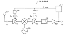
- FIG. 5 is a block diagram of the conventional receiving apparatus 101.
- the receiving apparatus 101 is a general direct conversion type receiving apparatus, and is integrated into an integrated circuit using a semiconductor.
- the receiving apparatus 101 in FIG. 5 is provided with an input terminal 102 for receiving signals and an output terminal 109.
- the reception apparatus 101 includes a high frequency variable gain amplifier 103, a frequency converter (mixer) 104, a low frequency variable gain amplifier 105, a low pass filter 106, an output amplifier 107, and a local signal generator (local signal generator) 108. Yes. Further, the receiving apparatus 101 includes an output signal level detection circuit 110, a first gain control circuit 111, and a second gain control circuit 112.
- the output of the antenna 160 connected to the receiving apparatus 101 is connected to the input of the high-frequency variable gain amplifier 103 via the input terminal 102.
- the output of the high frequency variable gain amplifier 103 is connected to the first input of the frequency converter 104.
- the output of the local signal generator 108 is connected to the second input of the frequency converter 104.
- the output of the frequency converter 104 is connected to the input of the low frequency variable gain amplifier 105.
- the output of the low frequency variable gain amplifier 105 is connected to the input of the low pass filter 106.
- the output of the low pass filter 106 is connected to the input of the output amplifier 107.
- the output of the output amplifier 107 is connected to the output terminal 109 and the input of the output signal level detection circuit 110.
- the output of the output signal level detection circuit 110 is connected to the input of the first gain control circuit 111 and the input of the second gain control circuit 112.
- the first output of the first gain control circuit 111 is connected to the first control input of the high frequency variable gain amplifier 103.
- the second output of the first gain control circuit 111 is connected to the second control input of the high-frequency variable gain amplifier 103.
- the first output of the second gain control circuit 112 is connected to the first control input of the low frequency variable gain amplifier 105.
- the second output of the second gain control circuit 112 is connected to the second control input of the low frequency variable gain amplifier 105.
- the high frequency variable gain amplifier 103 is a high frequency variable gain amplifier corresponding to a signal having a relatively high frequency before frequency conversion is performed by the frequency converter 104.
- the low frequency variable gain amplifier 105 is a low frequency variable gain amplifier corresponding to a signal having a relatively low frequency after frequency conversion is performed by the frequency converter 104.
- the first gain control circuit 111 supplies an FET control signal Sc-1 that is a signal for controlling on / off of the FET of the first distribution circuit included in the high-frequency variable gain amplifier 103 to the first control input of the high-frequency variable gain amplifier 103. Output.
- the first gain control circuit 111 outputs a control voltage Vc, which is a voltage for controlling the magnitude of the output current of the variable current source included in the high-frequency variable gain amplifier 103, to the second control input of the high-frequency variable gain amplifier 103.
- the FET control signal Sc-1 and the control voltage Vc constitute a first gain control signal.
- the second gain control circuit 112 uses the FET control signal Sc-2, which is a signal for controlling on / off of the FET of the first distribution circuit included in the low-frequency variable gain amplifier 105, as the first control of the low-frequency variable gain amplifier 105. Output to input.
- the second gain control circuit 112 outputs a control voltage Vc, which is a voltage for controlling the magnitude of the output current of the variable current source included in the low frequency variable gain amplifier 105, to the second control input of the high frequency variable gain amplifier 103.
- the FET control signal Sc-2 and the control voltage Vc constitute a second gain control signal.
- the output signal of the high frequency variable gain amplifier 103 is input to the first input of the frequency converter 104.
- the frequency converter 104 performs frequency conversion on the signal input to the first input by the local signal (local signal) output from the local signal generator 108 and input to the second input of the frequency converter 104. .
- a signal having a relatively low frequency after the frequency conversion is input to the low frequency variable gain amplifier 105 as an output signal of the frequency converter 104.
- the gain of the low frequency variable gain amplifier 105 is increased or decreased by the second gain control signal output from the second gain control circuit 112.
- the signal input to the low frequency variable gain amplifier 105 is amplified or attenuated by the low frequency variable gain amplifier 105. Therefore, the signal level of the signal output from the low frequency variable gain amplifier 105 becomes the predetermined first level.
- the output signal of the low frequency variable gain amplifier 105 is output to the low pass filter 106.
- the low pass filter 106 attenuates the high frequency component in the output signal of the low frequency variable gain amplifier 105, and outputs the signal after the attenuation of the high frequency component to the output amplifier 107.
- the output amplifier 107 amplifies the output signal of the low-pass filter 106, and generates the output signal of the output amplifier 107.
- the output signal of the output amplifier 107 is output to the outside of the receiving apparatus 101 via the output terminal 109 and also output to the output signal level detection circuit 110.
- the output signal level detection circuit 110 detects a predetermined second level which is the signal level of the output signal of the output amplifier 107 when the output signal of the output amplifier 107 is input.
- the second level is higher than the first level, which is the signal level of the output signal of the low frequency variable gain amplifier 105, for amplification by the output amplifier 107.
- the output signal level detection circuit 110 outputs the instruction signal S-order to the first gain control circuit 111 after detecting the second level.
- the instruction signal S-order is a signal corresponding to the second level, and is a signal that instructs generation of a signal and a voltage necessary for controlling the gain of the high-frequency variable gain amplifier 103.
- the output signal level detection circuit 110 outputs the instruction signal S-order to the second gain control circuit 112 after the second level is detected.
- the instruction signal S-order is a signal corresponding to the second level and is an instruction for generating a signal and a voltage necessary for controlling the gain of the low frequency variable gain amplifier 105.
- the instruction signal S-order is input from the output signal level detection circuit 110 to the first gain control circuit 111.
- the first gain control circuit 111 generates the FET control signal Sc-1 and outputs it to the first control input of the high-frequency variable gain amplifier 103, and also generates the control voltage Vc to generate the first control signal Vc of the high-frequency variable gain amplifier 103. 2 Output to control input.
- the gain of the high-frequency variable gain amplifier 103 is controlled (increased or decreased).
- the instruction signal S-order is input from the output signal level detection circuit 110 to the second gain control circuit 112.
- the second gain control circuit 112 generates the FET control signal Sc-2 and outputs it to the first control input of the low frequency variable gain amplifier 105, and also generates the control voltage Vc to generate the low frequency variable gain amplifier 105.
- the gain of the low frequency variable gain amplifier 105 is controlled (increased or decreased).
- the output signal level detection circuit 110, the first gain control circuit 111, and the second gain control circuit 112 are used to adjust the gain of the high frequency variable gain amplifier 103 and the low frequency variable gain amplifier.
- the gain of 105 is feedback controlled. Thereby, the maximum level of the signal level of the output signal output to the outside of the receiving apparatus 101 via the output terminal 109 can be set to the second level.
- the NF of the high-frequency variable gain amplifier 103 may be lowered. This is because the NF of the receiving apparatus 101 as a whole and the NF of the high-frequency variable gain amplifier 103 are substantially equal, and therefore, if the NF of the high-frequency variable gain amplifier 103 is determined, the NF of the receiving apparatus 101 as a whole is almost determined. It is.
- the receiving apparatus 101 in FIG. 5 as a whole needs high linearity.
- the linearity of the high-frequency variable gain amplifier 103 may be increased. This is because the linearity of the entire receiving apparatus 101 and the linearity of the high-frequency variable gain amplifier 103 are substantially equal. Therefore, if the linearity of the high-frequency variable gain amplifier 103 is determined, the linearity of the entire receiving apparatus 101 is approximately It is because it is decided.
- both the case where the signal level of the signal input to the high frequency variable gain amplifier 103 is low and the case where the signal level of the signal input to the high frequency variable gain amplifier 103 is high can be dealt with.
- the high-frequency variable gain amplifier 103 is required to have both low NF when the gain is high and high linearity when the gain is low.
- the gain change between the high frequency variable gain amplifier 103 and the low frequency variable gain amplifier 105 is “monotonous and continuous” (or the discontinuity is made sufficiently small). It is necessary.
- the gain change is monotonous and continuous.
- the gain of the high-frequency variable gain amplifier 103 changes in a linear function or in a quadratic function with respect to a change in the signal level of the input signal of the high-frequency variable gain amplifier 103, It can be said that it is a monotonous and continuous gain change.
- the gain of the low frequency variable gain amplifier 105 changes in a linear function or in a quadratic function with respect to a change in the signal level of the input signal of the low frequency variable gain amplifier 105, It can be said that it is a monotonous and continuous gain change.
- the gain of the high-frequency variable gain amplifier 103 changes exponentially or logarithmically with respect to the change in the signal level of the input signal of the high-frequency variable gain amplifier 103, it is monotonous. And it can be said that it is a continuous gain change.
- the gain of the low frequency variable gain amplifier 105 changes exponentially or logarithmically with respect to the change in signal level of the input signal of the low frequency variable gain amplifier 105, it is monotonous. And it can be said that it is a continuous gain change.
- “monotonous and continuous” in the present invention is not limited to the first to third examples of gain change. It should be noted that even if the change cannot be expressed simply, if the output voltage signal V does not reverse with respect to the change in the control voltage Vc and changes continuously in an analog manner, the change is monotonous and continuous. Suppose you are.
- a high-frequency variable gain amplifier (high-frequency variable gain amplifier 103 in FIG. 5) that realizes low NF when the gain is high, high linearity when the gain is low, and monotonous and continuous gain change is disclosed in Patent Literature 1 is disclosed.
- the variable gain amplifier of Patent Document 1 it is disclosed that a plurality of variable gain amplifiers are provided and the gains of the plurality of variable gain amplifiers are controlled stepwise.
- variable gain amplifier of Patent Document 1 discloses that a plurality of variable Gm circuits (variable conductance circuits) are provided and the conductances of the plurality of variable Gm circuits are controlled stepwise.
- Japanese Patent Publication Japanese Patent Laid-Open No. 2002-252532 (published on Sep. 06, 2002)”
- variable gain amplifier of Patent Document 1 includes a plurality of variable Gm circuits, and a plurality of variable Gm circuits are connected in parallel to control the conductance of the plurality of variable Gm circuits in a stepwise manner.
- variable gain amplifier does not change greatly even if the gain change is performed using the variable Gm circuit with respect to the variable Gm circuit that is not dominant in determining the gain.
- the gain change may not be monotonous (or the gain change may not be continuous) when the bias current of the variable Gm circuit is turned on / off at the point where the gain is switched.
- the bias current of the variable Gm circuit is gradually changed (slowly). Thereby, it is conceivable that the current output from the variable gain amplifier is gradually decreased (or gradually increased).
- CMOS transistor Complementary Metal-Oxide-Semiconductor transistor
- FIG. 6 is a circuit diagram of a conventional variable gain amplifier 113 configured by connecting two variable Gm circuits in parallel.
- the high frequency variable gain amplifier 103 of the receiving apparatus 101 of FIG. 5 includes the first variable Gm circuit 144 of FIG.
- the low frequency variable gain amplifier 105 of the receiving apparatus 101 in FIG. 5 includes the second variable Gm circuit 145 in FIG.
- variable gain amplifier 113 (Configuration of variable gain amplifier 113)
- the variable gain amplifier 113 shown in FIG. 6 includes a signal input terminal 114, a power supply terminal 115, an instruction signal input terminal 116, and a voltage signal output terminal 117.
- the signal input terminal 114 includes one signal input terminal 114a and the other signal input terminal 114b.
- the voltage signal output terminal 117 is composed of one voltage signal output terminal 117a and the other voltage signal output terminal 117b.
- variable gain amplifier 113 includes a control circuit 118, FETs (field-effect transistors) 119 to 130, variable current sources 131 and 132, and a DC voltage source 150.
- FETs field-effect transistors
- one end of the load 133 is connected to one voltage signal output terminal 117a, and the other end is connected to the output of the DC voltage source 150.
- the load 134 has one end connected to the other voltage signal output terminal 117 b and the other end connected to the output of the DC voltage source 150.
- the FETs 119 and 120 constitute a first Gm circuit 136.
- the FETs 125 and 126 constitute a second Gm circuit 138.
- the FETs 121 to 124 constitute a first distribution circuit 137.
- the FETs 127 to 130 constitute a second distribution circuit 139.
- variable current source 131 the variable current source 131, the first Gm circuit 136, and the first distribution circuit 137 constitute a first variable Gm circuit 144.
- variable current source 132, the second Gm circuit 138, and the second distribution circuit 139 constitute a second variable Gm circuit 145.
- one signal input terminal 114 a is connected to the gate of the FET 119 and the gate of the FET 125.
- the other signal input terminal 114 b is connected to the gate of the FET 120 and the gate of the FET 126.
- the source of the FET 119 and the source of the FET 120 are connected to the input of the variable current source 131.
- the source of the FET 125 and the source of the FET 126 are connected to the input of the variable current source 132.
- the drain of the FET 119 is connected to the source of the FET 121 and the source of the FET 122.
- the drain of the FET 120 is connected to the source of the FET 123 and the source of the FET 124.
- the drain of the FET 125 is connected to the source of the FET 127 and the source of the FET 128.
- the drain of the FET 126 is connected to the source of the FET 129 and the source of the FET 130.
- the drain of the FET 121 is connected to the drain of the FET 127, one voltage signal output terminal 117 a, and one end of the load 133.
- the drain of the FET 124 is connected to the drain of the FET 130, the other voltage signal output terminal 117 b, and one end of the load 134.
- the drain of the FET 122, the drain of the FET 123, the drain of the FET 128, the drain of the FET 129, the other end of the load 133, and the other end of the load 134 are connected to the output of the DC voltage source 150 through the power supply terminal 115.
- the first output of the control circuit 118 is connected to the control input of the variable current source 131.
- the second output of the control circuit 118 is connected to the control input of the variable current source 132.
- the third output of the control circuit 118 is connected to the gate of the FET 121 and the gate of the FET 124.
- the fourth output of the control circuit 118 is connected to the gate of the FET 122 and the gate of the FET 123.
- the fifth output of the control circuit 118 is connected to the gate of the FET 127 and the gate of the FET 130.
- the sixth output of the control circuit 118 is connected to the gate of the FET 128 and the gate of the FET 129.
- the output of the variable current source 131, the output of the variable current source 132, and the input of the DC voltage source 150 are electrically grounded.
- variable gain amplifier 113 In the variable gain amplifier 113 of FIG. 6, the instruction signal S-order is input to the instruction signal input terminal 116 of the control circuit 118.
- the instruction signal S-order is a signal for instructing generation of a signal and a voltage necessary for controlling the gain of the high frequency variable gain amplifier 103 and the gain of the low frequency variable gain amplifier 105.
- the control circuit 118 controls the target to which each control signal is input by generating the following control signals.
- control circuit 118 generates the control voltage Vc when the instruction signal is input. Then, the control circuit 118 outputs the control voltage Vc generated by itself to the control input of the variable current source 131 and the control input of the variable current source 132.
- the magnitude of the current I1 which is the current output from the variable current source 131 and is the bias current of the first variable Gm circuit 144, is controlled according to the magnitude of the control voltage Vc.
- the magnitude of the current I2 which is the current output from the variable current source 132 and is the bias current of the second variable Gm circuit 145, is controlled according to the magnitude of the control voltage Vc.
- control circuit 118 outputs the FET control signal Sc-1a from the third output of the control circuit 118 and receives the FET control from the fourth output of the control circuit 118 when the instruction signal is input.
- the signal Sc-1b is output.
- the FET control signal Sc-1a and the FET control signal Sc-1b constitute the FET control signal Sc-1.
- control circuit 118 outputs the FET control signal Sc-2a from the fifth output of the control circuit 118 and the FET control from the sixth output of the control circuit 118 when the instruction signal is input.
- the signal Sc-2b is output.
- the FET control signal Sc-2a and the FET control signal Sc-2b constitute an FET control signal Sc-2.
- the FETs 121 and 124 are turned on / off according to the FET control signal Sc-1a.
- the FETs 122 and 123 are turned on / off according to the FET control signal Sc-1b.
- the output current signals I-out1 and I-out2 are caused to flow to the first variable Gm circuit 144 via the loads 133 and 134, or the output current signals I-out1 and I-out2 are passed via the loads 133 and 134.
- the first variable Gm circuit 44 is assigned to the first variable Gm circuit 44.
- the FETs 127 and 130 are turned on / off according to the FET control signal Sc-2a.
- the FETs 128 and 129 are turned on / off according to the FET control signal Sc-2b.
- the output current signals I-out1 and I-out2 are caused to flow to the second variable Gm circuit 45 via the loads 133 and 134, or the output current signals I-out1 and I-out2 are sent to the loads 133 and 134. Whether or not to flow to the second variable Gm circuit 45 is determined.
- variable gain amplifier 113 of FIG. 6 an input signal Vin which is a voltage signal is input between one signal input terminal 114a and the other signal input terminal 114b.
- an input signal Vin which is a voltage signal is input between one signal input terminal 114a and the other signal input terminal 114b.
- the FETs included in the first Gm circuit 136 and the second Gm circuit 138 is controlled by the input signal Vin.
- the value of the current flowing through the first Gm circuit 136 and the value of the current flowing through the second Gm circuit 138 are determined, the value of the current flowing through the first variable Gm circuit 144 and the second variable Gm circuit 145 are determined. The value of the flowing current is determined.
- the maximum Gm of the first variable Gm circuit 144 is set lower than the maximum Gm of the second variable Gm circuit 145.
- variable gain amplifier 113 The operation of the variable gain amplifier 113 configured as described above will be described with reference to the graph of FIG.
- FIG. 7 is an explanatory diagram of the operation of the conventional variable gain amplifier 113, and (a) to (f) are graphs showing the operation of the conventional variable gain amplifier 113.
- FIG. 7A and 7D are graphs showing changes in the currents I1 and I2 output from the variable current sources 131 and 132 with respect to the control voltage Vc input to the control inputs of the variable current sources 131 and 132.
- FIG. 7B and 7E are graphs showing changes in the output current signal I-out1 and the output current signal I-out2 with respect to the control voltage Vc input to the control inputs of the variable current sources 131 and 132.
- FIG. . 7B and 7E the broken line indicates the output current signal I-out1 that is a current flowing through the load 133, and the alternate long and short dash line indicates the output current signal I-out2 that is a current flowing through the load 134. .
- FIG. 7 (c) and 7 (f) are graphs showing changes in the output voltage signal V of the variable gain amplifier 113 with respect to the control voltage Vc input to the control inputs of the variable current sources 131 and 132.
- FIG. 7B shows an output current signal I-out1 and an output current signal I-out2 with respect to the control voltage Vc when the variable current sources 131 and 132 are not turned on and off as shown in FIG. Shows changes.
- FIG. 7C shows a change in the output voltage signal V with respect to the control voltage Vc when the variable current sources 131 and 132 are not turned on / off as shown in FIG.
- variable current sources 131 and 132 are always on, power consumption is increased.
- the power supply voltage (the output voltage of the DC voltage source 50) is not sufficiently high and an element that generates a DC voltage drop, such as a resistor, is used as the loads 133 and 134.
- the gain is maximum (that is, when the output voltage signal V is maximum)
- the output current signal I-out1 and the output current signal I-out2 are both maximum, and the operating point is inappropriate. It becomes.
- variable current sources 131 and 132 are not always turned on, and an increase in power consumption can be prevented. Further, since the output current signal I-out1 and the output current signal I-out2 are not the maximum when the gain is maximum, an appropriate operating point can be obtained as an operating point. Furthermore, the minimum gain can be lowered (that is, the minimum value of the output voltage signal V can be reduced) as compared with the case where the variable current sources 131 and 132 are not turned on / off.
- the present invention has been made in view of the above-described conventional problems, and an object of the present invention is to provide a variable gain amplifier that can prevent deterioration of linearity and increase in power consumption.
- variable gain amplifier includes the first and second variable gain amplifiers and the first gain control signal that is a signal for controlling the gain of the first variable gain amplifier.
- a control circuit that outputs to the second variable gain amplifier a second gain control signal that is output to the variable gain amplifier and that controls the gain of the second variable gain amplifier; Includes a first variable conductance circuit that is a circuit having a variable conductance as a whole circuit, and the second variable gain amplifier includes a second variable conductance circuit that is a circuit having a variable conductance as a whole circuit.
- the maximum conductance value of the one variable conductance circuit is higher than the maximum conductance value of the second variable conductance circuit.
- the circuit steeply raises the output current of the first variable current source included in the first variable conductance circuit when the output current of the first variable conductance circuit is sufficiently smaller than the output current of the second variable conductance circuit. It is characterized by lowering.
- the output current of the second variable conductance circuit before the first variable conductance circuit is turned off is the output current of the first variable conductance circuit when the first variable conductance circuit is turned off. (Preferably sufficiently small).
- the first variable current source In this state, that is, in a state where the output current of the second variable conductance circuit is smaller than the output current of the first variable conductance circuit, the first variable current source is turned off and the first variable current source The output current is sharply lowered and the first variable conductance circuit is turned off.
- the first variable conductance circuit does not operate with a small bias current. Therefore, the variable gain amplifier can be operated in a state where the linearity is not deteriorated.
- the gain discontinuity when the output current of the first variable current source falls sharply is sufficiently small. Therefore, the discontinuity of the gain change can be sufficiently reduced.
- the output current of the first variable current source is sharply lowered at an appropriate timing. Therefore, it is possible to prevent an increase in power consumption caused by always operating the first variable current source.
- variable gain amplifier that can prevent deterioration in linearity and increase in power consumption.
- the variable gain amplifier includes the first and second variable gain amplifiers, the first gain control signal which is a signal for controlling the gain of the first variable gain amplifier, and the first variable gain amplifier. And a control circuit that outputs a second gain control signal, which is a signal for controlling the gain of the second variable gain amplifier, to the second variable gain amplifier, the first variable gain amplifier comprising: A first variable conductance circuit that is a circuit having a variable conductance as a whole; and the second variable gain amplifier includes a second variable conductance circuit that is a circuit having a variable conductance as a whole circuit, and the first variable conductance is provided.
- the maximum value of conductance of the circuit is higher than the maximum value of conductance of the second variable conductance circuit.
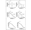
- FIG. 7 is an explanatory diagram of the operation of the variable gain amplifier according to the embodiment of the present invention
- (a) to (f) are graphs showing the operation of the conventional variable gain amplifier
- (g) to (o) It is a graph which shows operation
- 1 is a block diagram of a variable gain amplifier according to an embodiment of the present invention. 1 is a circuit diagram of a variable gain amplifier according to an embodiment of the present invention. It is a block diagram of the conventional receiver. It is a circuit diagram of the conventional variable gain amplifier.
- FIG. 6 is an explanatory diagram of the operation of a conventional variable gain amplifier
- FIGS. 5A to 5F are graphs showing the operation of a conventional variable gain amplifier.
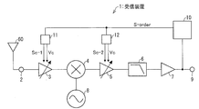
- FIG. 2 is a block diagram of the receiving device 1 according to the present embodiment.
- the receiving device 1 is a direct conversion type receiving device, and is integrated into an integrated circuit using a semiconductor.
- the receiving apparatus 1 of FIG. 2 is provided with an input terminal 2 for receiving signals and an output terminal 9.
- the receiving apparatus 1 also includes a high frequency variable gain amplifier 3, a frequency converter (mixer) 4, a low frequency variable gain amplifier 5, a low pass filter 6, an output amplifier 7, and a local signal generator (local signal generator) 8. Yes.
- the receiving device 1 includes an output signal level detection circuit 10, a first gain control circuit 11, and a second gain control circuit 12.
- the output of the antenna 60 connected to the receiving device 1 is connected to the input of the high-frequency variable gain amplifier 3 via the input terminal 2.
- the output of the high frequency variable gain amplifier 3 is connected to the first input of the frequency converter 4.
- the output of the local signal generator 8 is connected to the second input of the frequency converter 4.
- the output of the frequency converter 4 is connected to the input of the low frequency variable gain amplifier 5.
- the output of the low frequency variable gain amplifier 5 is connected to the input of the low pass filter 6.
- the output of the low-pass filter 6 is connected to the input of the output amplifier 7.
- the output of the output amplifier 7 is connected to the output terminal 9 and the input of the output signal level detection circuit 10.
- the output of the output signal level detection circuit 10 is connected to the input of the first gain control circuit 11 and the input of the second gain control circuit 12.
- the first output of the first gain control circuit 11 is connected to the first control input of the high-frequency variable gain amplifier 3.
- the second output of the first gain control circuit 11 is connected to the second control input of the high-frequency variable gain amplifier 3.
- the first output of the second gain control circuit 12 is connected to the first control input of the low frequency variable gain amplifier 5.
- the second output of the second gain control circuit 12 is connected to the second control input of the low frequency variable gain amplifier 5.
- the high frequency variable gain amplifier 3 is a high frequency variable gain amplifier corresponding to a signal having a relatively high frequency before frequency conversion is performed by the frequency converter 4.
- the low frequency variable gain amplifier 5 is a low frequency variable gain amplifier corresponding to a signal having a relatively low frequency after frequency conversion is performed by the frequency converter 4.
- the first gain control circuit 11 supplies an FET control signal Sc-1 that is a signal for controlling on / off of the FET of the first distribution circuit included in the high-frequency variable gain amplifier 3 to the first control input of the high-frequency variable gain amplifier 3. Output.
- the first gain control circuit 11 outputs a control voltage Vc, which is a voltage for controlling the magnitude of the output current of the variable current source included in the high frequency variable gain amplifier 3, to the second control input of the high frequency variable gain amplifier 3.
- the FET control signal Sc-1 and the control voltage Vc constitute a first gain control signal.
- the second gain control circuit 12 converts the FET control signal Sc-2, which is a signal for controlling on / off of the FET of the first distribution circuit included in the low frequency variable gain amplifier 5, into the first control of the low frequency variable gain amplifier 5. Output to input.
- the second gain control circuit 12 outputs a control voltage Vc, which is a voltage for controlling the magnitude of the output current of the variable current source included in the low frequency variable gain amplifier 5, to the second control input of the low frequency variable gain amplifier 5.
- the FET control signal Sc-2 and the control voltage Vc constitute a second gain control signal.
- the output signal of the high frequency variable gain amplifier 3 is input to the first input of the frequency converter 4.
- the frequency converter 4 performs frequency conversion on the signal input to the first input by the local signal (local signal) output from the local signal generator 8 and input to the second input of the frequency converter 4. .
- the signal having a relatively low frequency after the frequency conversion is input to the low frequency variable gain amplifier 5 as an output signal of the frequency converter 4.
- the gain of the low frequency variable gain amplifier 5 is increased or decreased by the second gain control signal output from the second gain control circuit 12.
- the signal input to the low frequency variable gain amplifier 5 is amplified or attenuated by the low frequency variable gain amplifier 5. Therefore, the signal level of the signal output from the low frequency variable gain amplifier 5 becomes the predetermined first level.
- the output signal of the low frequency variable gain amplifier 5 is output to the low pass filter 6.
- the low pass filter 6 attenuates the high frequency component in the output signal of the low frequency variable gain amplifier 5 and outputs the signal after the attenuation of the high frequency component to the output amplifier 7.
- the output amplifier 7 amplifies the output signal of the low-pass filter 6 and generates the output signal of the output amplifier 7.
- the output signal of the output amplifier 7 is output to the outside of the receiving device 1 through the output terminal 9 and also output to the output signal level detection circuit 10.
- the output signal level detection circuit 10 detects a predetermined second level which is the signal level of the output signal of the output amplifier 7 when the output signal of the output amplifier 7 is input.
- the second level is higher than the first level, which is the signal level of the output signal of the low frequency variable gain amplifier 5, due to amplification by the output amplifier 7.
- the output signal level detection circuit 10 instructs generation of a signal and a voltage that are signals corresponding to the second level and are necessary for controlling the gain of the high-frequency variable gain amplifier 3 after the detection of the second level.
- An instruction signal S-order which is a signal is output to the first gain control circuit 11. Further, the output signal level detection circuit 10 generates a signal and a voltage corresponding to the second level, which are necessary for controlling the gain of the low frequency variable gain amplifier 5 after the detection of the second level. Is output to the second gain control circuit 12 as an instruction signal S-order.
- the first gain control circuit 11 receives the instruction signal S-order from the output signal level detection circuit 10. Thereby, the first gain control circuit 11 generates the FET control signal Sc-1 and outputs it to the first control input of the high-frequency variable gain amplifier 3, and also generates the control voltage Vc to generate the first control signal Vc of the high-frequency variable gain amplifier 3. 2 Output to control input. Thereby, the gain of the high-frequency variable gain amplifier 3 is controlled (increased or decreased).
- the instruction signal S-order is input from the output signal level detection circuit 10 to the second gain control circuit 12.
- the second gain control circuit 12 generates the FET control signal Sc-2 and outputs it to the first control input of the low frequency variable gain amplifier 5, and also generates the control voltage Vc to generate the low frequency variable gain amplifier 5 To the second control input.
- the gain of the low frequency variable gain amplifier 5 is controlled (increased or decreased).
- the output signal level detection circuit 10, the first gain control circuit 11, and the second gain control circuit 12 use the gain of the high frequency variable gain amplifier 3 and the low frequency variable gain amplifier.
- a gain of 5 is feedback controlled.
- the receiving apparatus 1 since the receiving apparatus 1 according to the present embodiment includes any of the variable gain amplifiers 13 described below, it is possible to prevent deterioration in linearity and increase in power consumption.
- variable gain amplifier 13 the variable gain amplifier 13 in the present embodiment will be described below with reference to FIGS.
- the high-frequency variable gain amplifier 3 (first variable gain amplifier) of the receiving apparatus 1 of FIG. 2 includes the first variable Gm circuit (first variable conductance circuit) 44 of FIGS.
- the low frequency variable gain amplifier 5 (second variable gain amplifier) of the receiving apparatus 1 of FIG. 2 includes the second variable Gm circuit (second variable conductance circuit) 45 of FIGS.
- the first variable Gm circuit 44 and the second variable Gm circuit 45 are circuits having a variable Gm (variable conductance) as a whole circuit.
- Gm in the present embodiment indicates transconductance.
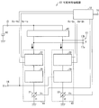
- FIG. 3 is a block diagram of the variable gain amplifier 13 according to the present embodiment.
- the variable gain amplifier 13 of FIG. 3 is provided with a signal input terminal 14, a power supply terminal 15, an instruction signal input terminal 16, and a voltage signal output terminal 17.
- the voltage signal output terminal 17 is composed of one voltage signal output terminal 17a and the other voltage signal output terminal 17b.
- variable gain amplifier 13 includes a control circuit 18, a variable current source 31 (first variable current source), and a variable current source 32 (second variable current source). Further, the variable gain amplifier 13 includes a first Gm circuit (first conductance circuit) 36, a first distribution circuit 37, a second Gm circuit (second conductance circuit) 38, a second distribution circuit 39, a load circuit 40, and a DC voltage. A source 50 is provided.
- variable current source 31 the first Gm circuit 36, and the first distribution circuit 37 constitute a first variable Gm circuit 44.
- variable current source 32, the second Gm circuit 38, and the second distribution circuit 39 constitute a second variable Gm circuit 45.
- the signal input terminal 14 is connected to the control input of the first Gm circuit 36 and the control input of the second Gm circuit 38.
- the output of the first Gm circuit 36 is connected to the input of the variable current source 31.
- the output of the second Gm circuit 38 is connected to the input of the variable current source 32.
- the output of the first distribution circuit 37 is connected to the input of the first Gm circuit 36.
- the output of the second distribution circuit 39 is connected to the input of the second Gm circuit 38.
- the input of the first distribution circuit 37 is connected to the first output of the load circuit 40 and one voltage signal output terminal 17a.
- the input of the second distribution circuit 39 is connected to the second output of the load circuit 40 and the other voltage signal output terminal 17b.
- the first input of the load circuit 40 and the first input of the load circuit 40 are connected to the output of the DC voltage source 50 via the power supply terminal 15.
- the first output of the control circuit 18 is connected to the control input of the variable current source 31.
- the second output of the control circuit 18 is connected to the control input of the variable current source 32.
- the third output of the control circuit 18 is connected to the first control input of the first distribution circuit 37.
- the fourth output of the control circuit 18 is connected to the second control input of the first distribution circuit 37.
- the fifth output of the control circuit 18 is connected to the first control input of the second distribution circuit 39.
- the sixth output of the control circuit 18 is connected to the second control input of the second distribution circuit 39.
- the output of the variable current source 31, the output of the variable current source 32, and the input of the DC voltage source 50 are electrically grounded.
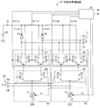
- FIG. 4 is a circuit diagram of the variable gain amplifier 13 according to the present embodiment.
- the high frequency variable gain amplifier 3 of the receiving apparatus 1 of FIG. 2 includes the first variable Gm circuit 44 of FIG.
- the low frequency variable gain amplifier 5 of the receiving apparatus 1 of FIG. 2 includes the second variable Gm circuit 45 of FIG.
- the variable gain amplifier 13 shown in FIG. 1 includes a signal input terminal 14, a power supply terminal 15, an instruction signal input terminal 16, and a voltage signal output terminal 17.
- the variable gain amplifier 13 shown in FIG. 1 includes a signal input terminal 14, a power supply terminal 15, an instruction signal input terminal 16, and a voltage signal output terminal 17.
- the signal input terminal 14 includes one signal input terminal 14a and the other signal input terminal 14b. Furthermore, the voltage signal output terminal 17 is composed of one voltage signal output terminal 17a and the other voltage signal output terminal 17b.
- variable gain amplifier 13 includes a control circuit 18, FETs (field-effect transistors, first FET to twelfth FETs) 19 to 30, variable current sources 31 and 32, and a DC voltage source 50. .
- the load 33 (first load) has one end connected to one voltage signal output terminal 17a and the other end connected to the output of the DC voltage source 50.
- one end of the load 34 (second load) is connected to the other voltage signal output terminal 17b, and the other end is connected to the output of the DC voltage source 50.
- Loads 33 and 34 are differential pair loads. When the loads 33 and 34 are resistors, the resistance value of the load 33 is equal to the resistance value of the load 34. Further, the loads 33 and 34 are not limited to resistors. When considering the high-frequency component of the signal, as the loads 33 and 34, (1) an inductor, (2) an inductor and a resistor connected in series, or (3) an inductor and a resistor connected in parallel Is used. By using the above (1) to (3) as the loads 33 and 34, the frequency characteristics can be adjusted.
- the FETs 19 and 20 constitute a first Gm circuit 36.
- the FETs 25 and 26 constitute a second Gm circuit 38.
- the FETs 21 to 24 constitute a first distribution circuit 37.
- the FETs 27 to 30 constitute a second distribution circuit 39.
- variable current source 31 the first Gm circuit 36, and the first distribution circuit 37 constitute a first variable Gm circuit 44.
- variable current source 32, the second Gm circuit 38, and the second distribution circuit 39 constitute a second variable Gm circuit 45.
- first variable Gm circuit 44 and the second variable Gm circuit 45 share the loads 33 and 34, respectively.
- sharing of the loads 33 and 34 is not essential. That is, one load may be provided for the first variable Gm circuit 44 and another one load may be provided for the second variable Gm circuit 45.
- the output of the first variable Gm circuit 44 and the output of the second variable Gm circuit 45 may be individually connected to the load circuit 40.
- the connection point between the output of the first variable Gm circuit 44 and the load circuit 40 and the connection point between the output of the second variable Gm circuit 45 and the load circuit 40 individually are output nodes.
- one signal input terminal 14 a is connected to the gate of the FET 19 and the gate of the FET 25.
- the other signal input terminal 14 b is connected to the gate of the FET 20 and the gate of the FET 26.
- the source of the FET 19 and the source of the FET 20 are connected to the input of the variable current source 31.
- the source of the FET 25 and the source of the FET 26 are connected to the input of the variable current source 32.
- the drain of the FET 19 is connected to the source of the FET 21 and the source of the FET 22.
- the drain of the FET 20 is connected to the source of the FET 23 and the source of the FET 24.
- the drain of the FET 25 is connected to the source of the FET 27 and the source of the FET 28.
- the drain of the FET 26 is connected to the source of the FET 29 and the source of the FET 30.
- the drain of the FET 21 is connected to the drain of the FET 27, one voltage signal output terminal 17 a, and one end of the load 33.
- the drain of the FET 24 is connected to the drain of the FET 30, the other voltage signal output terminal 17 b, and one end of the load 34.
- the drain of the FET 22, the drain of the FET 23, the drain of the FET 28, the drain of the FET 29, the other end of the load 33, and the other end of the load 34 are connected to the output of the DC voltage source 50 through the power supply terminal 15.
- the first output of the control circuit 18 is connected to the control input of the variable current source 31.
- the second output of the control circuit 18 is connected to the control input of the variable current source 32.
- the third output of the control circuit 18 is connected to the gate of the FET 21 and the gate of the FET 24.
- the fourth output of the control circuit 18 is connected to the gate of the FET 22 and the gate of the FET 23.
- the fifth output of the control circuit 18 is connected to the gate of the FET 27 and the gate of the FET 30.
- the sixth output of the control circuit 18 is connected to the gate of the FET 28 and the gate of the FET 29.
- the output of the variable current source 31, the output of the variable current source 32, and the input of the DC voltage source 50 are electrically grounded.
- variable gain amplifier 13 (Correspondence between block diagram of FIG. 3 and circuit diagram of FIG. 4)
- the variable gain amplifier 13 is shown in a block diagram in FIG. 3 and in a circuit diagram in FIG.
- some of the components that handle differential signals specifically, the first Gm circuit 36, the second Gm circuit 38, the first distribution circuit 37, and the second distribution circuit 39 are In the block diagram of FIG. 3, it is described as a single-ended component.
- the single-ended component refers to a component that handles a differential signal as a single signal.
- 3 is a circuit including the loads 33 and 34 of FIG.
- the instruction signal S-order is input to the instruction signal input terminal 16 of the control circuit 18.
- the instruction signal S-order is a signal for instructing generation of a signal and a voltage necessary for controlling the gain of the high-frequency variable gain amplifier 3 and the gain of the low-frequency variable gain amplifier 5.
- the control circuit 18 controls the target to which each control signal is input by generating the following control signals.
- control circuit 18 generates the control voltage Vc when the instruction signal is input. Then, the control circuit 18 outputs the control voltage Vc generated by itself to the control input of the variable current source 31 and the control input of the variable current source 32.
- the magnitude of the current I1 which is the current output from the variable current source 31 and is the bias current of the first variable Gm circuit 44, is controlled according to the magnitude of the control voltage Vc.
- the magnitude of the current I2 which is the current output from the variable current source 32 and is the bias current of the second variable Gm circuit 45, is controlled according to the magnitude of the control voltage Vc.
- control circuit 18 outputs the FET control signal Sc-1a (second FET control signal) from the third output of the control circuit 18 in response to the input of the instruction signal. From the output, an FET control signal Sc-1b (third FET control signal) is output.
- the FET control signal Sc-1a and the FET control signal Sc-1b constitute an FET control signal Sc-1 (first FET control signal).
- control circuit 18 outputs the FET control signal Sc-2a (fifth FET control signal) from the fifth output of the control circuit 18 by the input of the instruction signal, and the sixth of the control circuit 18 From the output, an FET control signal Sc-2b (sixth FET control signal) is output.
- the FET control signal Sc-2a and the FET control signal Sc-2b constitute an FET control signal Sc-2 (fourth FET control signal).
- the FETs 21 and 24 are turned on / off according to the FET control signal Sc-1a.
- the FETs 22 and 23 are turned on / off according to the FET control signal Sc-1b.
- the output current signals I-out1 and I-out2 are passed through the first variable Gm circuit 44 through the loads 33 and 34, or the output current signals I-out1 and I-out2 are passed through the loads 33 and 34.
- the first variable Gm circuit 44 is assigned to the first variable Gm circuit 44.
- the output current signals I-out1 and I-out2 are differential currents. Further, the signal components of the output current signals I-out1 and I-out2 have the same amplitude but have a phase difference of 180 degrees. Further, the DC components of the output current signals I-out1 and I-out2 have the same value.
- the FETs 27 and 30 are turned on / off according to the FET control signal Sc-2a.
- the FETs 28 and 29 are turned on / off according to the FET control signal Sc-2b.
- the output current signals I-out1 and I-out2 are caused to flow to the second variable Gm circuit 45 via the loads 33 and 34, or the output current signals I-out1 and I-out2 are sent to the loads 33 and 34. Whether or not to flow to the second variable Gm circuit 45 is determined.
- variable gain amplifier 113 of FIG. 6 an input signal Vin which is a voltage signal is input between one signal input terminal 14a and the other signal input terminal 14b.
- Vin On / off of the FETs included in the first Gm circuit 36 and the second Gm circuit 38 is controlled by the input signal Vin.
- the value of the current flowing through the first Gm circuit 36 and the value of the current flowing through the second Gm circuit 38 are determined, so that the value of the current flowing through the first variable Gm circuit 44 and the second variable Gm circuit 45 are The value of the flowing current is determined.
- the maximum Gm (maximum conductance) of the first variable Gm circuit 44 is set higher than the maximum Gm (maximum conductance) of the second variable Gm circuit 45.
- the current I1 output from the variable current source 31 is the output current of the first variable Gm circuit 44 (the drain current of the FETs 21 and 24), and the output current of the second variable Gm circuit 45.
- the current I1 output from the variable current source 31 is sharply lowered when the output current of the first distribution circuit 37 is smaller than the output current of the second distribution circuit 39 (preferably when it is sufficiently small).
- the current I2 output from the variable current source 31 rises sharply when the output current of the second variable Gm circuit 45 is smaller than the output current of the first variable Gm circuit 44 (preferably when it is sufficiently small).
- variable Gm circuit 44 and the second variable Gm circuit 45 do not operate with a small bias current. Therefore, it is possible to provide the variable gain amplifier 13 that can prevent deterioration of linearity and increase in power consumption.
- variable gain amplifier 13 Details of the operation of the variable gain amplifier 13 according to the present embodiment will be described based on the graph of FIG.
- FIG. 1 is an explanatory diagram of the operation of the variable gain amplifier 13 according to the present embodiment.
- FIGS. 1A to 1F are graphs showing the operation of the conventional variable gain amplifier 113, and
- FIGS. ) Is a graph showing the operation of the variable gain amplifier 13 according to the present embodiment.
- FIG. 1 show changes in the currents I1 and I2 output from the variable current sources 31 and 32 with respect to the control voltage Vc input to the control inputs of the variable current sources 31 and 32, respectively. It is a graph to show.
- (H), (k), and (n) of FIG. 1 show changes in the output current signal I-out1 and the output current signal I-out2 with respect to the control voltage Vc input to the control inputs of the variable current sources 31 and 32. It is a graph to show.
- the broken line indicates the output current signal I-out1 that is the current flowing through the load 33
- the alternate long and short dash line indicates the output current signal I that is the current flowing through the load 34. Indicates -out2.
- the two-dot chain line will be described later.
- FIG. 1 are graphs showing changes in the output voltage signal V of the variable gain amplifier 13 with respect to the control voltage Vc input to the control inputs of the variable current sources 31 and 32. . That is, the output voltage signal V is a signal output from the voltage signal output terminal 17 of FIGS.
- variable gain amplifier 13 the control of the current I1 output from the variable current source 31 is different from the control of the current I1 output from the variable current source 131 of the conventional variable gain amplifier 113.
- variable gain amplifier 13 the control of the current I2 output from the variable current source 32 is different from the control of the current I2 output from the variable current source 132 of the conventional variable gain amplifier 113. .
- variable gain amplifier 13 Control in the variable gain amplifier 13 according to the present embodiment will be described below with reference to (g) to (o) of FIG.
- the current I1 output from the variable current source 31 does not gradually change. That is, the current I1 output from the variable current source 31 is turned off at the predetermined control voltage Vc (falls sharply).
- the current I2 output from the variable current source 32 does not gradually change. That is, the current I2 output from the variable current source 32 is turned on (steeply rises) at a predetermined control voltage Vc.
- FIG. 1 (h) shows changes in the output current signal I-out1 and the output current signal I-out2 with respect to the control voltage Vc when the currents I1 and I2 are controlled as shown in FIG. 1 (g). It is a graph. Further, (i) of FIG. 1 is a graph showing a change of the output voltage signal V with respect to the control voltage Vc when the currents I1 and I2 are controlled as shown in (g) of FIG.
- variable current source 32 In this state, that is, in a state where the output current signal I-out2 is sufficiently smaller than the output current signal I-out1, the variable current source 32 is turned on to rapidly increase the current I2, and the second variable Gm circuit Turn on 45.
- the control voltage Vc1 when the second variable Gm circuit 45 is turned on is a control voltage in which Gm of the variable gain amplifier 13 as a whole is determined by the first variable Gm circuit 44.
- the output current signal I-out1 before the first variable Gm circuit 44 is turned off is the output current signal I-out2 of the second variable Gm circuit 45 at the control voltage Vc2 when the first variable Gm circuit 44 is turned off.
- variable current source 31 In this state, that is, in a state where the output current signal I-out1 is sufficiently smaller than the output current signal I-out2, the variable current source 31 is turned off and the current I1 falls sharply, and the first variable Gm circuit 44 is turned off.
- the control voltage Vc2 when the first variable Gm circuit 44 is turned off is a control voltage in which Gm of the variable gain amplifier 13 as a whole is determined by the second variable Gm circuit 45.
- variable current source 31 is turned off and the current I1 is sharply lowered and the first The variable Gm circuit 44 is turned off.
- the first variable Gm circuit 44 and the second variable Gm circuit 45 do not operate with a small bias current. Therefore, the linearity does not deteriorate, and the variable gain amplifier 13 can be operated in a state in which good linearity is maintained over the entire range of the control voltage Vc.
- the gain discontinuity between when the current I1 is off and when the current I2 is on is sufficiently small. Therefore, the discontinuity of the gain change can be sufficiently reduced.
- the current I1 of the variable current source 31 is turned off at an appropriate timing, and the current I2 of the variable current source 32 is turned on at an appropriate timing. Therefore, it is possible to prevent an increase in power consumption caused by always operating the variable current sources 31 and 32.
- variable gain amplifier 13 that can prevent deterioration of linearity and increase in power consumption.
- the current I1 output from the variable current source 31 is gradually changed before turning off. That is, before the current I1 is turned off, the current I1 is gradually reduced to a value that does not deteriorate the linearity.
- the current I2 output from the variable current source 32 is gradually changed after being turned on. That is, by turning on at a predetermined control voltage Vc, the current increases to a current having good linearity, and the current is gradually increased after being turned on.
- control of the currents I1 and I2 shown in (j) of FIG. 1 combines on / off and gradually changing.
- the current I1 is turned off at the control voltage Vc2 and does not gradually change.
- the current I2 is turned on at the control voltage Vc1, and does not gradually change.
- the current I1 is at the control voltage Vc4 lower than the control voltage Vc2. Turn off. That is, the control voltage Vc when the current I1 output from the variable current source 31 sharply falls is made different within a range where the output current signal I-out1 is smaller than the output current signal I-out2.
- the control voltage Vc4 is lower than the control voltage Vc2, but the current I1 may be turned off with a control voltage higher than the control voltage Vc2. Thereby, a gain different from the gain when the current I1 is turned off at the control voltages Vc2 and Vc4 can be obtained.
- the current I2 can be controlled in the same manner as the current I1.
- the current I2 is at a control voltage Vc3 higher than the control voltage Vc1. Turn on. That is, the control voltage Vc when the current I2 output from the variable current source 32 rises sharply is made different within a range where the output current signal I-out2 is smaller than the output current signal I-out1.
- the control voltage Vc3 is higher than the control voltage Vc1, but the current I2 may be turned on with a control voltage lower than the control voltage Vc1. Thereby, a gain different from that when the current I2 is turned on in the control voltages Vc1 and Vc3 can be obtained.
- the receiving apparatus 1 according to the present embodiment in FIG. 2 can include the variable gain amplifier 13 according to the present embodiment.
- the first variable gain amplifier configured by including the variable Gm circuit 44 of FIGS. 3 and 4 is applied as the high frequency variable gain amplifier 3 of FIG. 2, and the low frequency variable gain amplifier 5 of FIG.
- a second variable gain amplifier configured with the variable Gm circuit 45 may be applied. Thereby, deterioration of linearity and increase in power consumption can be prevented.
- the control circuit includes a second variable current source included in the second variable conductance circuit when an output current of the second variable conductance circuit is smaller than an output current of the first variable conductance circuit.
- the output current may be sharply raised.
- the second variable current source In a state where the output current of the first variable conductance circuit is smaller than the output current of the second variable conductance circuit, the second variable current source is turned on, and the output current of the second variable current source is sharpened. At the same time, the second variable conductance circuit is turned on.
- variable gain amplifier can be operated in a state where the linearity is not deteriorated.
- the gain discontinuity when the output current of the second variable current source is sharply raised is sufficiently small. Therefore, the discontinuity of the gain change can be sufficiently reduced.
- the output current of the second variable current source is suddenly started at an appropriate timing. Therefore, it is possible to prevent an increase in power consumption caused by always operating the second variable current source.
- variable gain amplifier that can prevent deterioration in linearity and increase in power consumption.
- variable gain amplifiers In any one of the variable gain amplifiers, a signal input terminal, a power supply terminal, and a voltage signal output terminal are provided, and the first variable conductance circuit outputs an output in accordance with a control voltage output from the control circuit.
- a first variable current source that changes a voltage value to be applied, a first conductance circuit that determines a bias current according to an output current of the first variable current source, an output current of the first variable conductance circuit, and a first load and A first distribution circuit that distributes or distributes the output current of the first variable conductance circuit without passing through the first load and the second load;
- the circuit includes a second variable current source that changes a value of an output current in accordance with a control voltage output from the control circuit, and an output current of the second variable current source.
- the first conductance circuit includes a first FET and a second FET, and the second conductance circuit includes a seventh FET and an eighth FET.
- the first distribution circuit has third to sixth FETs, and the second distribution circuit has ninth to twelfth FETs.
- the one signal input terminal is connected to the gate of the first FET and the gate of the second FET, and the other signal input terminal is connected to the gate of the seventh FET and the gate of the eighth FET,
- the source of the first FET and the source of the second FET are connected to the input of the first variable current source, and the source of the seventh FET and the source of the eighth FET are the second variable current source.
- the drain of the first FET is connected to the source of the third FET and the source of the fourth FET, and the drain of the second FET is connected to the source of the fifth FET and the second FET.
- the drain of the seventh FET 25 is connected to the source of the ninth FET and the source of the tenth FET, and is connected to the source of the 6FET.
- the drain of the eighth FET is connected to the source of the eleventh FET and the source of the twelfth FET, and the drain of the third FET is the drain of the ninth FET, the one voltage signal output terminal, and the first voltage signal output terminal.
- the drain of the sixth FET is connected to the drain of the twelfth FET, the other voltage signal output terminal, and one end of the second load, and the drain of the fourth FET is connected to one end of the load.
- the drain of the fifth FET, the drain of the tenth FET, the drain of the eleventh FET, the other end of the first load, and the other end of the second load are connected to the output of the DC voltage source through the power supply terminal.
- a first output of the control circuit is connected to a control input of the first variable current source, and a second output of the control circuit is connected to the second variable current source.
- the third output of the control circuit is connected to the gate of the third FET and the gate of the sixth FET, and the fourth output of the control circuit is the gate of the fourth FET.
- the fifth output of the control circuit is connected to the gate of the ninth FET and the gate of the twelfth FET, and the sixth output of the control circuit is The gate of the tenth FET and the gate of the eleventh FET are connected, and the output of the first variable current source, the output of the second variable current source, and the input of the DC voltage source are electrically It may be grounded.
- an instruction signal which is a signal for instructing generation of a signal and a voltage necessary for controlling the gain of the first variable gain amplifier and the gain of the second variable gain amplifier, The signal is input to the instruction signal input terminal of the control circuit.
- the control circuit controls the object to which each control signal is input by generating the following control signals.
- control circuit generates the control voltage when the instruction signal is input.
- the control circuit outputs the control voltage generated by itself to the control input of the first variable current source and the control input of the second variable current source.
- the magnitude of the output current of the first variable current source is controlled according to the magnitude of the control voltage.
- the magnitude of the output current of the second variable current source is controlled according to the magnitude of the control voltage.
- control circuit outputs the second FET control signal from the third output of the control circuit and the second FET control signal from the fourth output of the control circuit when the instruction signal is input. Is output.
- the second FET control signal and the third FET control signal constitute a first FET control signal.
- control circuit outputs a fifth FET control signal from the fifth output of the control circuit and receives a sixth FET control signal from the sixth output of the control circuit when the instruction signal is input. Is output.
- the fifth FET control signal and the sixth FET control signal constitute a fourth FET control signal.
- the third FET and the sixth FET are turned on / off according to the second FET control signal.
- the fourth FET and the fifth FET are turned on / off according to the third FET control signal.
- the output current of the first variable conductance circuit is caused to flow to the first variable conductance circuit via the first and second loads, or the output current of the first variable conductance circuit is supplied to the first and second variables. Whether the current flows through the first variable conductance circuit without passing through two loads is determined.
- the current flows through the following path. That is, the output of the DC voltage source ⁇ the fourth FET ⁇ the first FET ⁇ the first variable current source ⁇ GND and the output of the DC voltage source ⁇ the fifth FET ⁇ the second FET ⁇ the first variable current source. ⁇ Current flows through the GND path.
- the ninth FET and the twelfth FET are turned on / off in response to the fifth FET control signal.
- the tenth FET and the eleventh FET are turned on / off in response to the sixth FET control signal.
- the output current of the second variable conductance circuit is caused to flow to the second variable conductance circuit via the first and second loads, or the output current of the second variable conductance circuit is supplied to the first and second variables. Whether to flow to the second variable conductance circuit without passing through two loads is assigned.
- the current flows through the following path. That is, the output of the DC voltage source ⁇ the 10th FET ⁇ the 7th FET ⁇ the second variable current source ⁇ GND and the output of the DC voltage source ⁇ the 11th FET ⁇ the 8th FET ⁇ the 2nd variable current source. ⁇ Current flows through the GND path.
- variable gain amplifier an input signal which is a voltage signal is input between the one signal input terminal and the other signal input terminal.
- the on / off of the FETs included in the first conductance circuit and the second conductance circuit is controlled by the input signal.
- the value of the current flowing through the first conductance circuit and the value of the current flowing through the second conductance circuit are determined, the value of the current flowing through the first variable conductance circuit and the second variable conductance are determined. The value of the current flowing through the circuit is determined.
- the output current of the first variable current source is selected when the output current of the first variable conductance circuit is smaller than the output current of the second variable conductance circuit (preferably sufficient). When it is small, it falls sharply. That is, the output current of the first variable current source falls sharply when the output current of the first distribution circuit is smaller (preferably sufficiently small) than the output current of the second distribution circuit. At the same time, the output current of the second variable current source rises sharply when the output current of the second variable conductance circuit is smaller (preferably sufficiently small) than the output current of the first variable conductance circuit. .
- the first and second variable conductance circuits do not operate with a small bias current. Therefore, it is possible to provide a variable gain amplifier that can prevent deterioration in linearity and increase in power consumption.
- the control voltage when the output current of the first variable current source sharply falls is different within a range where the current flowing through the first load is smaller than the current flowing through the second load. It may be allowed.
- the output current of the first variable current source is set to be less than the control voltage. Also falls sharply at high control voltages.
- the control voltage when the output current of the second variable current source is sharply raised is different in a range where the current flowing through the second load is smaller than the current flowing through the first load. It may be allowed.
- the output current of the second variable current source can be obtained from the control voltage. Also falls sharply at a low control voltage.
- the output current of the first variable current source may be gradually decreased before the output current of the first variable current source sharply falls.
- the output current of the second variable current source may be gradually increased after the output current of the second variable current source is sharply raised.
- variable gain amplifier that ensures good linearity while ensuring gain continuity and does not increase power consumption.
- the control circuit is a signal for instructing generation of a signal and a voltage necessary for controlling the gain of the first variable gain amplifier and the gain of the second variable gain amplifier.
- the first gain control signal is output to the first variable gain amplifier and is a signal for controlling the gain of the second variable gain amplifier.
- a second gain control signal may be output to the second variable gain amplifier.
- control circuit can control the gains of the first and second variable gain amplifiers.
- the receiving apparatus of the present invention includes any of the variable gain amplifiers described above, it is possible to prevent deterioration in linearity and increase in power consumption.
- variable gain amplifier of the present invention can be applied to a receiving device.
- it can be suitably used for a receiving apparatus that receives a digital satellite broadcast.
Landscapes
- Control Of Amplification And Gain Control (AREA)
- Amplifiers (AREA)
- Circuits Of Receivers In General (AREA)
Abstract
第1可変利得増幅器は、回路全体としての可変コンダクタンスを有する回路である第1可変コンダクタンス回路を備え、第2可変利得増幅器は、第2可変コンダクタンス回路を備え、上記第1可変コンダクタンス回路のコンダクタンスの最大値は、上記第2可変コンダクタンス回路のコンダクタンスの最大値よりも高く、上記第1可変コンダクタンス回路の出力電流が、上記第2可変コンダクタンス回路の出力電流よりも小さい時に、上記第1可変コンダクタンス回路が備える第1可変電流源が出力する電流(I1)を急峻に立ち下げる。
Description
本発明は可変利得増幅器に関するものであり、特に半導体集積回路上に集積されて利得を自動で制御することに使用される可変利得増幅器に関する。
半導体集積回路で用いられて、利得の制御が可能である可変利得増幅器は、例えば、デジタル衛星放送を受信する受信装置が備える半導体集積回路において用いられる。
図5は、従来の受信装置101のブロック図である。受信装置101は、一般的なダイレクトコンバージョン型の受信装置であって、半導体を用いて集積回路化されている。
〔受信装置101〕
(受信装置101の構成)
図5の受信装置101は、受信信号の入力端子102と、出力端子109とが設けられている。また、受信装置101は、高周波可変利得増幅器103、周波数変換器(ミキサ)104、低周波可変利得増幅器105、ローパスフィルタ106、出力増幅器107、ローカル信号生成器(局所信号生成器)108を備えている。さらに、受信装置101は、出力信号レベル検出回路110、第1利得制御回路111、及び、第2利得制御回路112を備えている。
(受信装置101の構成)
図5の受信装置101は、受信信号の入力端子102と、出力端子109とが設けられている。また、受信装置101は、高周波可変利得増幅器103、周波数変換器(ミキサ)104、低周波可変利得増幅器105、ローパスフィルタ106、出力増幅器107、ローカル信号生成器(局所信号生成器)108を備えている。さらに、受信装置101は、出力信号レベル検出回路110、第1利得制御回路111、及び、第2利得制御回路112を備えている。
図5の受信装置101において、受信装置101に接続されたアンテナ160の出力が、入力端子102を介して、高周波可変利得増幅器103の入力に接続されている。高周波可変利得増幅器103の出力は、周波数変換器104の第1入力に接続されている。ローカル信号生成器108の出力は、周波数変換器104の第2入力に接続されている。
周波数変換器104の出力は、低周波可変利得増幅器105の入力に接続されている。低周波可変利得増幅器105の出力は、ローパスフィルタ106の入力に接続されている。ローパスフィルタ106の出力は、出力増幅器107の入力へ接続されている。
出力増幅器107の出力は、出力端子109と、出力信号レベル検出回路110の入力とに接続されている。出力信号レベル検出回路110の出力は、第1利得制御回路111の入力と、第2利得制御回路112の入力とに接続されている。
第1利得制御回路111の第1出力は、高周波可変利得増幅器103の第1制御入力に接続されている。第1利得制御回路111の第2出力は、高周波可変利得増幅器103の第2制御入力に接続されている。第2利得制御回路112の第1出力は、低周波可変利得増幅器105の第1制御入力に接続されている。そして、第2利得制御回路112の第2出力は、低周波可変利得増幅器105の第2制御入力に接続されている。
高周波可変利得増幅器103は、周波数変換器104によって周波数変換がなされる前の、周波数が比較的高い信号に対応する高周波可変利得増幅器である。
低周波可変利得増幅器105は、周波数変換器104によって周波数変換がなされた後の、周波数が比較的低い信号に対応する低周波可変利得増幅器である。
第1利得制御回路111は、高周波可変利得増幅器103が備える第1振り分け回路のFETのオン・オフを制御する信号であるFET制御信号Sc-1を、高周波可変利得増幅器103の第1制御入力へ出力する。また、第1利得制御回路111は、高周波可変利得増幅器103が備える可変電流源の出力電流の大小を制御する電圧である制御電圧Vcを、高周波可変利得増幅器103の第2制御入力へ出力する。FET制御信号Sc-1及び制御電圧Vcは、第1利得制御信号を構成する。
第2利得制御回路112は、低周波可変利得増幅器105が備える第1振り分け回路のFETのオン・オフを制御する信号であるFET制御信号Sc-2を、低周波可変利得増幅器105の第1制御入力へ出力する。また、第2利得制御回路112は、低周波可変利得増幅器105が備える可変電流源の出力電流の大小を制御する電圧である制御電圧Vcを、高周波可変利得増幅器103の第2制御入力へ出力する。FET制御信号Sc-2及び制御電圧Vcは、第2利得制御信号を構成する。
(受信装置101の動作)
図5の受信装置101では、アンテナ160が受信する信号であって、入力端子102を介して高周波可変利得増幅器103に入力される受信信号は、高周波可変利得増幅器103によって、増幅されるか、減衰される。
図5の受信装置101では、アンテナ160が受信する信号であって、入力端子102を介して高周波可変利得増幅器103に入力される受信信号は、高周波可変利得増幅器103によって、増幅されるか、減衰される。
高周波可変利得増幅器103の出力信号は、周波数変換器104の第1入力に入力される。周波数変換器104は、ローカル信号生成器108から出力されて周波数変換器104の第2入力に入力されるローカル信号(局所信号)により、第1入力に入力された信号に対して周波数変換を行う。周波数変換がなされた後の、周波数が比較的低い信号は、周波数変換器104の出力信号として、低周波可変利得増幅器105に入力される。
低周波可変利得増幅器105は、第2利得制御回路112から出力される第2利得制御信号によって、利得が増減される。これにより、低周波可変利得増幅器105に入力される信号は、低周波可変利得増幅器105によって、増幅されるか、減衰される。従って、低周波可変利得増幅器105から出力される信号の信号レベルが、所定の第1レベルとなる。
低周波可変利得増幅器105の出力信号は、ローパスフィルタ106に出力される。ローパスフィルタ106は、低周波可変利得増幅器105の出力信号における高周波成分を減衰して、高周波成分を減衰した後の信号を、出力増幅器107に出力する。
出力増幅器107は、ローパスフィルタ106の出力信号を増幅して、出力増幅器107の出力信号を生成する。出力増幅器107の出力信号は、出力端子109を介して受信装置101の外部へ出力されるとともに、出力信号レベル検出回路110に出力される。
出力信号レベル検出回路110は、出力増幅器107の出力信号が入力されることにより、出力増幅器107の出力信号の信号レベルである所定の第2レベルを検出する。当該第2レベルは、出力増幅器107による増幅のために、低周波可変利得増幅器105の出力信号の信号レベルである上記第1レベルよりも高い。
出力信号レベル検出回路110は、第2レベルの検出後に、指示信号S-orderを第1利得制御回路111に出力する。指示信号S-orderは、第2レベルに応じた信号であって、高周波可変利得増幅器103の利得を制御するために必要である、信号及び電圧の生成を指示する信号である。
また、出力信号レベル検出回路110は、第2レベルの検出後に、指示信号S-orderを第2利得制御回路112に出力する。指示信号S-orderは、第2レベルに応じた信号であって、低周波可変利得増幅器105の利得を制御するために必要である、信号及び電圧の生成を指示する信号である。
第1利得制御回路111には、出力信号レベル検出回路110から指示信号S-orderが入力される。これにより、第1利得制御回路111は、FET制御信号Sc-1を生成して高周波可変利得増幅器103の第1制御入力へ出力するとともに、制御電圧Vcを生成して高周波可変利得増幅器103の第2制御入力へ出力する。これにより、高周波可変利得増幅器103の利得が制御される(増減される)。
同様に、第2利得制御回路112には、出力信号レベル検出回路110から指示信号S-orderが入力される。これにより、第2利得制御回路112は、FET制御信号Sc-2を生成して低周波可変利得増幅器105の第1制御入力へ出力するとともに、制御電圧Vcを生成して低周波可変利得増幅器105の第2制御入力へ出力する。これにより、低周波可変利得増幅器105の利得が制御される(増減される)。
以上のように、図5の受信装置101では、出力信号レベル検出回路110、第1利得制御回路111、及び、第2利得制御回路112によって、高周波可変利得増幅器103の利得と低周波可変利得増幅器105の利得とがフィードバック制御される。これにより、出力端子109を介して受信装置101の外部に出力される出力信号の信号レベルの最大レベルを、第2レベルにすることが出来る。
ここで、高周波可変利得増幅器103に入力される信号の信号レベルが低い場合を考える。この場合、図5の受信装置101全体として、低いNF(noise figure:雑音指数)が必要となる。
入力信号レベルが低い場合、即ち、高い利得が必要な場合には、高周波可変利得増幅器103のNFを低くすればよい。何故なら、受信装置101全体としてのNFと、高周波可変利得増幅器103のNFとが略等しいので、高周波可変利得増幅器103のNFを定めれば、受信装置101全体としてのNFが概ね決定されるためである。
また、入力信号レベルが高い場合には、図5の受信装置101全体として、高い線形性が必要となる。
入力信号レベルが高い場合、即ち、低い利得が必要な場合には、高周波可変利得増幅器103の線形性を高くすればよい。何故なら、受信装置101全体としての線形性と、高周波可変利得増幅器103の線形性とが略等しいので、高周波可変利得増幅器103の線形性を定めれば、受信装置101全体としての線形性が概ね決定されるためである。
上述したように、高周波可変利得増幅器103に入力される信号の信号レベルが低い場合と、高周波可変利得増幅器103に入力される信号の信号レベルが高い場合との両方に対応することが出来るように設計された場合を考える。この場合、高周波可変利得増幅器103には、利得が高い場合における低いNFと、利得が低い場合における高い線形性との両者が要求される。
さらに、フィードバック制御による安定した動作を実現するために、高周波可変利得増幅器103と低周波可変利得増幅器105との利得変化は、「単調かつ連続的」であること(または不連続を十分に小さくすること)が必要である。
ここで、単調かつ連続的な利得変化の例を3つ示す。
第1例として、高周波可変利得増幅器103の入力信号の信号レベルと、高周波可変利得増幅器103の利得とが、比例する場合、または、反比例する場合、単調かつ連続的な利得変化であると言える。
同様に、低周波可変利得増幅器105の入力信号の信号レベルと、低周波可変利得増幅器105の利得とが、比例する場合、または、反比例する場合、単調かつ連続的な利得変化であると言える。
第2例として、高周波可変利得増幅器103の入力信号の信号レベルの変化に対して、高周波可変利得増幅器103の利得が、一次関数的に変化する場合、または、二次関数的に変化する場合、単調かつ連続的な利得変化であると言える。
同様に、低周波可変利得増幅器105の入力信号の信号レベルの変化に対して、低周波可変利得増幅器105の利得が、一次関数的に変化する場合、または、二次関数的に変化する場合、単調かつ連続的な利得変化であると言える。
但し、二次関数的に変化する場合は、変数の符号が変化しないことが求められる。
第3例として、高周波可変利得増幅器103の入力信号の信号レベルの変化に対して、高周波可変利得増幅器103の利得が、指数関数的に変化する場合、または、対数関数的に変化する場合、単調かつ連続的な利得変化であると言える。
同様に、低周波可変利得増幅器105の入力信号の信号レベルの変化に対して、低周波可変利得増幅器105の利得が、指数関数的に変化する場合、または、対数関数的に変化する場合、単調かつ連続的な利得変化であると言える。
但し、本発明における「単調かつ連続的」とは、利得変化についての上記第1例~第3例に限定されない。なお、単純に数式化できない変化であっても、制御電圧Vcの変化に対して出力電圧信号Vが逆転せずにアナログ的に連続的な変化していれば、「単調かつ連続的」に変化しているものとする。
上述した単純に数式化できない変化は、図7の(c),(f)の出力電圧信号V、及び、図1の(c),(f),(i),(l),(o)の出力電圧信号Vに示される。図7及び図1については後述する。
高周波可変利得増幅器(図5の高周波可変利得増幅器103)において、利得が高い場合における低いNF、利得が低い場合における高い線形性、及び、単調かつ連続的な利得変化を実現するものが、特許文献1に開示されている。特許文献1の可変利得増幅器では、可変利得増幅器を複数備え、複数の可変利得増幅器の利得を、段階的に制御することが開示されている。
また、特許文献1の可変利得増幅器では、可変Gm回路(可変コンダクタンス回路)を複数備え、複数の可変Gm回路のコンダクタンスを、段階的に制御することも開示されている。
上述したように、特許文献1の可変利得増幅器では、可変Gm回路を複数備え、複数の可変Gm回路を並列接続して、複数の可変Gm回路のコンダクタンスを、段階的に制御する。これにより、利得が高い場合における低いNF、利得が低い場合における高い線形性、及び、単調かつ連続的な利得変化を実現することが出来る。
しかし、複数の可変Gm回路を常に動作させることは、消費電力の増大を招く。
そこで、複数の可変Gm回路の内、利得の決定に支配的でない可変Gm回路の動作を停止させて、消費電力の増大を抑制することが考えられる。
なお、利得の決定に支配的でない可変Gm回路に関して、当該可変Gm回路を用いて利得変化を行ったとしても、可変利得増幅器全体としての利得は、大きくは変化しない。
しかし、利得が切り替わる点において、可変Gm回路のバイアス電流をオン、オフすると、利得変化が単調ではなくなる場合がある(または利得変化が連続的ではなくなる場合がある)。
利得変化が単調ではなくなること、及び、利得変化が連続的ではなくなることを防ぐためには、可変Gm回路のバイアス電流を徐々に(なだらかに)変化させる。これにより、可変利得増幅器から外部に出力され電流を、徐々に減らしていく(または徐々に増やしていく)ことが考えられる。
しかし、CMOSトランジスタ(Complementary Metal-Oxide-Semiconductor transistor:相補性金属酸化膜半導体トランジスタ)を用いた可変Gm回路において、バイアス電流を徐々に変化させると、以下の問題が生じる。即ち、バイアス電流が小さい領域において、可変利得増幅器全体の線形性が悪化する。
可変利得増幅器全体における線形性の悪化について、図6を用いて以下に説明する。図6は、2つの可変Gm回路を並列接続して構成された従来の可変利得増幅器113の回路図である。図5の受信装置101の高周波可変利得増幅器103は、図6の第1可変Gm回路144を備えている。同様に、図5の受信装置101の低周波可変利得増幅器105は、図6の第2可変Gm回路145を備えている。
〔可変利得増幅器113〕
(可変利得増幅器113の構成)
図6の可変利得増幅器113には、信号入力端子114、電源端子115、指示信号入力端子116、及び、電圧信号出力端子117が設けられている。
(可変利得増幅器113の構成)
図6の可変利得増幅器113には、信号入力端子114、電源端子115、指示信号入力端子116、及び、電圧信号出力端子117が設けられている。
また、図6の可変利得増幅器113では、信号入力端子114は、一方の信号入力端子114aと他方の信号入力端子114bとから構成されている。さらに、電圧信号出力端子117は、一方の電圧信号出力端子117aと他方の電圧信号出力端子117bとから構成されている。
さらに、可変利得増幅器113は、制御回路118、FET(field-effect transistor:電界効果トランジスタ)119~130、可変電流源131,132、及び、直流電圧源150を備えている。
さらに、負荷133は、一端が、一方の電圧信号出力端子117aに接続されており、他端が、直流電圧源150の出力に接続されている。同様に、負荷134は、一端が、他方の電圧信号出力端子117bに接続されており、他端が、直流電圧源150の出力に接続されている。
なお、FET119,120は、第1Gm回路136を構成する。FET125,126は、第2Gm回路138を構成する。FET121~124は、第1振り分け回路137を構成する。FET127~130は、第2振り分け回路139を構成する。
また、可変電流源131、第1Gm回路136、及び、第1振り分け回路137は、第1可変Gm回路144を構成する。同様に、可変電流源132、第2Gm回路138、及び、第2振り分け回路139は、第2可変Gm回路145を構成する。
図6の可変利得増幅器113において、一方の信号入力端子114aは、FET119のゲートと、FET125のゲートとに接続されている。他方の信号入力端子114bは、FET120のゲートと、FET126のゲートとに接続されている。
FET119のソースと、FET120のソースとは、可変電流源131の入力に接続されている。FET125のソースと、FET126のソースとは、可変電流源132の入力に接続されている。
FET119のドレインは、FET121のソースと、FET122のソースとに接続されている。FET120のドレインは、FET123のソースと、FET124のソースとに接続されている。FET125のドレインは、FET127のソースと、FET128のソースとに接続されている。FET126のドレインは、FET129のソースと、FET130のソースとに接続されている。
FET121のドレインは、FET127のドレインと、一方の電圧信号出力端子117aと、負荷133の一端とに接続されている。FET124のドレインは、FET130のドレインと、他方の電圧信号出力端子117bと、負荷134の一端とに接続されている。
FET122のドレイン、FET123のドレイン、FET128のドレイン、FET129のドレイン、負荷133の他端、及び、負荷134の他端は、電源端子115を介して直流電圧源150の出力に接続されている。
制御回路118の第1出力は、可変電流源131の制御入力に接続されている。制御回路118の第2出力は、可変電流源132の制御入力に接続されている。
制御回路118の第3出力は、FET121のゲートと、FET124のゲートとに接続されている。制御回路118の第4出力は、FET122のゲートと、FET123のゲートとに接続されている。
制御回路118の第5出力は、FET127のゲートと、FET130のゲートとに接続されている。制御回路118の第6出力は、FET128のゲートと、FET129のゲートとに接続されている。
そして、可変電流源131の出力、可変電流源132の出力、及び、直流電圧源150の入力は、電気的に接地されている。
(可変利得増幅器113の動作)
図6の可変利得増幅器113では、指示信号S-orderが、制御回路118の指示信号入力端子116に入力される。指示信号S-orderは、高周波可変利得増幅器103の利得と低周波可変利得増幅器105の利得とを制御するために必要である、信号及び電圧の生成を指示する信号である。
図6の可変利得増幅器113では、指示信号S-orderが、制御回路118の指示信号入力端子116に入力される。指示信号S-orderは、高周波可変利得増幅器103の利得と低周波可変利得増幅器105の利得とを制御するために必要である、信号及び電圧の生成を指示する信号である。
制御回路118は、以下の各制御信号を生成することにより、各制御信号が入力される対象に対して制御を行う。
第1に、制御回路118は、上記指示信号が入力されることにより、制御電圧Vcを生成する。そして、制御回路118は、自身が生成した制御電圧Vcを、可変電流源131の制御入力と、可変電流源132の制御入力とに出力する。
制御電圧Vcの大小に応じて、可変電流源131が出力する電流であって、第1可変Gm回路144のバイアス電流である電流I1の大小が制御される。同様に、制御電圧Vcの大小に応じて、可変電流源132が出力する電流であって、第2可変Gm回路145のバイアス電流である電流I2の大小が制御される。
第2に、制御回路118は、上記指示信号が入力されることにより、制御回路118の第3出力から、FET制御信号Sc-1aを出力するとともに、制御回路118の第4出力から、FET制御信号Sc-1bを出力する。FET制御信号Sc-1a及びFET制御信号Sc-1bは、FET制御信号Sc-1を構成する。
第3に、制御回路118は、上記指示信号が入力されることにより、制御回路118の第5出力から、FET制御信号Sc-2aを出力するとともに、制御回路118の第6出力から、FET制御信号Sc-2bを出力する。FET制御信号Sc-2a及びFET制御信号Sc-2bは、FET制御信号Sc-2を構成する。
さらに、第1振り分け回路137では、FET制御信号Sc-1aに応じて、FET121,124がオン・オフされる。同様に、第1振り分け回路137では、FET制御信号Sc-1bに応じて、FET122,123がオン・オフされる。
これにより、出力電流信号I-out1,I-out2を、負荷133,134を介して第1可変Gm回路144に流すか、出力電流信号I-out1,I-out2を、負荷133,134を介さずに第1可変Gm回路44に流すかが振り分けられる。
出力電流信号I-out1及び出力電流信号I-out2を第1可変Gm回路144に流さない場合は、以下の経路で電流が流れる。即ち、直流電圧源150の出力→FET122→FET119→可変電流源131→GNDの経路と、直流電圧源150の出力→FET123→FET120→可変電流源131→GNDの経路とに電流が流れる。
さらに、第2振り分け回路139では、FET制御信号Sc-2aに応じて、FET127,130がオン・オフされる。同様に、第2振り分け回路139では、FET制御信号Sc-2bに応じて、FET128,129がオン・オフされる。
これにより、出力電流信号I-out1,I-out2を、負荷133,134を介して第2可変Gm回路45に流すに流すか、出力電流信号I-out1,I-out2を、負荷133,134を介さずに第2可変Gm回路45に流すかが振り分けられる。
出力電流信号I-out1及び出力電流信号I-out2を第1可変Gm回路145に流さない場合は、以下の経路で電流が流れる。即ち、直流電圧源150の出力→FET128→FET125→可変電流源132→GNDの経路と、直流電圧源150の出力→FET129→FET126→可変電流源132→GNDの経路とに電流が流れる。
さらに、図6の可変利得増幅器113では、一方の信号入力端子114aと他方の信号入力端子114bとの間に、電圧信号である入力信号Vinが入力される。入力信号Vinにより、第1Gm回路136と第2Gm回路138とが有するFETのオン・オフが制御される。
これにより、第1Gm回路136に流れる電流の値と、第2Gm回路138に流れる電流の値とが決定されるので、第1可変Gm回路144に流れる電流の値と、第2可変Gm回路145に流れる電流の値とが決定される。
ここで、第1可変Gm回路144の最大Gmは、第2可変Gm回路145の最大Gmよりも低くする。
このようにして構成された可変利得増幅器113の動作を、図7のグラフに基づいて説明する。
図7は、従来の可変利得増幅器113の動作の説明図であり、(a)~(f)は、従来の可変利得増幅器113の動作を示すグラフである。
図7の(a),(d)は、可変電流源131,132の制御入力に入力される制御電圧Vcに対する、可変電流源131,132が出力する電流I1,I2の変化を示すグラフである。
図7の(b),(e)は、可変電流源131,132の制御入力に入力される制御電圧Vcに対する、出力電流信号I-out1及び出力電流信号I-out2の変化を示すグラフである。図7の(b),(e)において、破線は、負荷133に流れる電流である出力電流信号I-out1を示し、一点鎖線は、負荷134に流れる電流である出力電流信号I-out2を示す。
図7の(c),(f)は、可変電流源131,132の制御入力に入力される制御電圧Vcに対する、可変利得増幅器113の出力電圧信号Vの変化を示すグラフである。出力電圧信号Vは、即ち、図6の電圧信号出力端子117から出力される信号である。
図7の(b)は、図7の(a)に示されるように可変電流源131,132をオン・オフしない場合の、制御電圧Vcに対する出力電流信号I-out1及び出力電流信号I-out2の変化を示す。図7の(c)は、図7の(a)に示されるように可変電流源131,132をオン・オフしない場合の、制御電圧Vcに対する出力電圧信号Vの変化を示す。
従来の可変利得増幅器113が、図7の(a)~(c)に示す動作を行う場合を考える。この場合、利得の制御の過程で不連続な点が生じることは無い。よって、出力電圧信号Vは、単調かつ連続的に制御される。
しかし、可変電流源131,132は常にオンしているので、消費電力の増加を招く。
また、電源電圧(直流電圧源50の出力電圧)が十分に高くなく、負荷133,134として、抵抗のような直流電圧降下を発生する素子を使用している場合を考える。この場合、利得が最大である時(即ち、出力電圧信号Vが最大である時)に、出力電流信号I-out1及び出力電流信号I-out2が共に最大となり、動作点が不適切な動作点となる。
なお、出力電流信号I-out1及び出力電流信号I-out2が共に最大である時は、即ち、第1可変Gm回路144及び第2可変Gm回路145の出力電流が共に最大である。
次に、図7の(d)示されるように、電流I1,I2を徐々に変化させた場合を考える。この場合、制御電圧Vcに対する出力電流信号I-out1及び出力電流信号I-out2の変化は、図7の(e)で示され、制御電圧Vcに対する出力電圧信号Vの変化は、図7の(f)で示される。
電流I1,I2を徐々に変化させるので、可変電流源131,132が常にオンしていることはなくなり、消費電力の増加を防ぐことが出来る。また、利得が最大である時に、出力電流信号I-out1及び出力電流信号I-out2が共に最大ではないので、動作点として適切な動作点が得られる。さらに、可変電流源131,132をオン・オフしない場合と比較して、最小利得を下げることが出来る(即ち、出力電圧信号Vの最小値を小さくすることが出来る)。
しかし、電流I1,I2を徐々に変化させる過程で、電流I1,I2が最小値付近となるので、第1Gm回路136、及び、第2Gm回路138を、小さなバイアス電流で動作させる状況が発生する。これに伴い、第1Gm回路136と第2Gm回路138との間における相互変調歪みIM3,IM2などで示される、可変利得増幅器113の線形性が悪化する。
なお、第1電流振り分け回路137における入力から出力への経路と、第2電流振り分け回路139における入力から出力への経路とが十分に分離されている場合を考える。この場合は、上述した相互変調歪みIM3,IM2などで示される非線形成分は、電圧信号出力端子117には現れない。
しかし、第1電流振り分け回路137と第2電流振り分け回路139とにおいてCMOSトランジスタを用いた場合を考える。この場合に、第1電流振り分け回路137における入力から出力への経路と、第2電流振り分け回路139における入力から出力への経路との間を、完全に分離することは困難である。
本発明は、上記従来の問題点に鑑みなされたものであって、その目的は、線形性の悪化と、消費電力の増大とを防ぐことが出来る可変利得増幅器を提供することにある。
本発明の可変利得増幅器は、上記課題を解決するために、第1及び第2可変利得増幅器と、上記第1可変利得増幅器の利得を制御する信号である第1利得制御信号を、上記第1可変利得増幅器に出力するとともに、上記第2可変利得増幅器の利得を制御する信号である第2利得制御信号を、上記第2可変利得増幅器に出力する制御回路とを備え、上記第1可変利得増幅器は、回路全体としての可変コンダクタンスを有する回路である第1可変コンダクタンス回路を備え、上記第2可変利得増幅器は、回路全体としての可変コンダクタンスを有する回路である第2可変コンダクタンス回路を備え、上記第1可変コンダクタンス回路のコンダクタンスの最大値は、上記第2可変コンダクタンス回路のコンダクタンスの最大値よりも高く、上記制御回路は、上記第1可変コンダクタンス回路の出力電流が、上記第2可変コンダクタンス回路の出力電流よりも十分に小さい時に、上記第1可変コンダクタンス回路が備える第1可変電流源の出力電流を急峻に立ち下げることを特徴とする。
上記発明によれば、上記第1可変コンダクタンス回路がオフする前の、上記第2可変コンダクタンス回路の出力電流は、上記第1可変コンダクタンス回路がオフするときの、上記第1可変コンダクタンス回路の出力電流に比べて小さい(好ましくは十分に小さい)。
この状態、即ち、上記第2可変コンダクタンス回路の出力電流が、上記第1可変コンダクタンス回路の出力電流に比べて小さい状態で、上記第1可変電流源をオフして、上記第1可変電流源の出力電流を急峻に立ち下げるとともに、上記第1可変コンダクタンス回路をオフする。
これにより、上記第1可変コンダクタンス回路が、小さいバイアス電流で動作することはない。よって、線形性が悪化しない状態で、上記可変利得増幅器を動作させることが出来る。
また、上記第1可変電流源の出力電流を急峻に立ち下げる時における利得の不連続は、十分に小さい。よって、利得変化の不連続も、十分小さくすることができる。
さらに、上記第1可変電流源の出力電流が、適切なタイミングで急峻に立ち下げられる。よって、上記第1可変電流源を常に動作させることによる消費電力の増大も防ぐことが出来る。
従って、線形性の悪化と、消費電力の増大とを防ぐことが出来る可変利得増幅器を提供することが出来る。
本発明の可変利得増幅器は、以上のように、第1及び第2可変利得増幅器と、上記第1可変利得増幅器の利得を制御する信号である第1利得制御信号を、上記第1可変利得増幅器に出力するとともに、上記第2可変利得増幅器の利得を制御する信号である第2利得制御信号を、上記第2可変利得増幅器に出力する制御回路とを備え、上記第1可変利得増幅器は、回路全体としての可変コンダクタンスを有する回路である第1可変コンダクタンス回路を備え、上記第2可変利得増幅器は、回路全体としての可変コンダクタンスを有する回路である第2可変コンダクタンス回路を備え、上記第1可変コンダクタンス回路のコンダクタンスの最大値は、上記第2可変コンダクタンス回路のコンダクタンスの最大値よりも高く、上記制御回路は、上記第1可変コンダクタンス回路の出力電流が、上記第2可変コンダクタンス回路の出力電流よりも十分に小さい時に、上記第1可変コンダクタンス回路が備える第1可変電流源の出力電流を急峻に立ち下げるものである。
それゆえ、線形性の悪化と、消費電力の増大とを防ぐことが出来る可変利得増幅器を提供するという効果を奏する。
本発明の一実施形態について図1~図4に基づいて説明すれば、以下の通りである。まずは、本実施形態に係る受信装置1について、図2を用いて説明する。図2は、本実施形態に係る受信装置1のブロック図である。受信装置1は、ダイレクトコンバージョン型の受信装置であって、半導体を用いて集積回路化されている。
〔受信装置1〕
(受信装置1の構成)
図2の受信装置1は、受信信号の入力端子2と、出力端子9とが設けられている。また、受信装置1は、高周波可変利得増幅器3、周波数変換器(ミキサ)4、低周波可変利得増幅器5、ローパスフィルタ6、出力増幅器7、ローカル信号生成器(局所信号生成器)8を備えている。さらに、受信装置1は、出力信号レベル検出回路10、第1利得制御回路11、及び、第2利得制御回路12を備えている。
(受信装置1の構成)
図2の受信装置1は、受信信号の入力端子2と、出力端子9とが設けられている。また、受信装置1は、高周波可変利得増幅器3、周波数変換器(ミキサ)4、低周波可変利得増幅器5、ローパスフィルタ6、出力増幅器7、ローカル信号生成器(局所信号生成器)8を備えている。さらに、受信装置1は、出力信号レベル検出回路10、第1利得制御回路11、及び、第2利得制御回路12を備えている。
図2の受信装置1において、受信装置1に接続されたアンテナ60の出力が、入力端子2を介して、高周波可変利得増幅器3の入力に接続されている。高周波可変利得増幅器3の出力は、周波数変換器4の第1入力に接続されている。ローカル信号生成器8の出力は、周波数変換器4の第2入力に接続されている。
周波数変換器4の出力は、低周波可変利得増幅器5の入力に接続されている。低周波可変利得増幅器5の出力は、ローパスフィルタ6の入力に接続されている。ローパスフィルタ6の出力は、出力増幅器7の入力へ接続されている。
出力増幅器7の出力は、出力端子9と、出力信号レベル検出回路10の入力とに接続されている。出力信号レベル検出回路10の出力は、第1利得制御回路11の入力と、第2利得制御回路12の入力とに接続されている。
第1利得制御回路11の第1出力は、高周波可変利得増幅器3の第1制御入力に接続されている。第1利得制御回路11の第2出力は、高周波可変利得増幅器3の第2制御入力に接続されている。第2利得制御回路12の第1出力は、低周波可変利得増幅器5の第1制御入力に接続されている。そして、第2利得制御回路12の第2出力は、低周波可変利得増幅器5の第2制御入力に接続されている。
高周波可変利得増幅器3は、周波数変換器4によって周波数変換がなされる前の、周波数が比較的高い信号に対応する高周波可変利得増幅器である。
低周波可変利得増幅器5は、周波数変換器4によって周波数変換がなされた後の、周波数が比較的低い信号に対応する低周波可変利得増幅器である。
第1利得制御回路11は、高周波可変利得増幅器3が備える第1振り分け回路のFETのオン・オフを制御する信号であるFET制御信号Sc-1を、高周波可変利得増幅器3の第1制御入力へ出力する。また、第1利得制御回路11は、高周波可変利得増幅器3が備える可変電流源の出力電流の大小を制御する電圧である制御電圧Vcを高周波可変利得増幅器3の第2制御入力へ出力する。FET制御信号Sc-1及び制御電圧Vcは、第1利得制御信号を構成する。
第2利得制御回路12は、低周波可変利得増幅器5が備える第1振り分け回路のFETのオン・オフを制御する信号であるFET制御信号Sc-2を、低周波可変利得増幅器5の第1制御入力へ出力する。また、第2利得制御回路12は、低周波可変利得増幅器5が備える可変電流源の出力電流の大小を制御する電圧である制御電圧Vcを、低周波可変利得増幅器5の第2制御入力へ出力する。FET制御信号Sc-2及び制御電圧Vcは、第2利得制御信号を構成する。
(受信装置1の動作)
図2の受信装置1では、アンテナ60が受信する信号であって、入力端子2を介して高周波可変利得増幅器3に入力される受信信号は、高周波可変利得増幅器3によって、増幅されるか、減衰される。
図2の受信装置1では、アンテナ60が受信する信号であって、入力端子2を介して高周波可変利得増幅器3に入力される受信信号は、高周波可変利得増幅器3によって、増幅されるか、減衰される。
高周波可変利得増幅器3の出力信号は、周波数変換器4の第1入力に入力される。周波数変換器4は、ローカル信号生成器8から出力されて周波数変換器4の第2入力に入力されるローカル信号(局所信号)により、第1入力に入力された信号に対して周波数変換を行う。周波数変換がなされた後の、周波数が比較的低い信号は、周波数変換器4の出力信号として、低周波可変利得増幅器5に入力される。
低周波可変利得増幅器5は、第2利得制御回路12から出力される第2利得制御信号によって、利得が増減される。これにより、低周波可変利得増幅器5に入力される信号は、低周波可変利得増幅器5によって、増幅されるか、減衰される。従って、低周波可変利得増幅器5から出力される信号の信号レベルが、所定の第1レベルとなる。
低周波可変利得増幅器5の出力信号は、ローパスフィルタ6に出力される。ローパスフィルタ6は、低周波可変利得増幅器5の出力信号における高周波成分を減衰して、高周波成分を減衰した後の信号を、出力増幅器7に出力する。
出力増幅器7は、ローパスフィルタ6の出力信号を増幅して、出力増幅器7の出力信号を生成する。出力増幅器7の出力信号は、出力端子9を介して受信装置1の外部へ出力されるとともに、出力信号レベル検出回路10に出力される。
出力信号レベル検出回路10は、出力増幅器7の出力信号が入力されることにより、出力増幅器7の出力信号の信号レベルである所定の第2レベルを検出する。当該第2レベルは、出力増幅器7による増幅のために、低周波可変利得増幅器5の出力信号の信号レベルである上記第1レベルよりも高い。
出力信号レベル検出回路10は、第2レベルの検出後に、第2レベルに応じた信号であって、高周波可変利得増幅器3の利得を制御するために必要である、信号及び電圧の生成を指示する信号である指示信号S-orderを、第1利得制御回路11に出力する。また、出力信号レベル検出回路10は、第2レベルの検出後に、第2レベルに応じた信号であって、低周波可変利得増幅器5の利得を制御するために必要である、信号及び電圧の生成を指示する信号である指示信号S-orderを、第2利得制御回路12に出力する。
第1利得制御回路11には、出力信号レベル検出回路10から指示信号S-orderが入力される。これにより、第1利得制御回路11は、FET制御信号Sc-1を生成して高周波可変利得増幅器3の第1制御入力へ出力するとともに、制御電圧Vcを生成して高周波可変利得増幅器3の第2制御入力へ出力する。これにより、高周波可変利得増幅器3の利得が制御される(増減される)。
同様に、第2利得制御回路12には、出力信号レベル検出回路10から指示信号S-orderが入力される。これにより、第2利得制御回路12は、FET制御信号Sc-2を生成して低周波可変利得増幅器5の第1制御入力へ出力するとともに、制御電圧Vcを生成して低周波可変利得増幅器5の第2制御入力へ出力する。これにより、低周波可変利得増幅器5の利得が制御される(増減される)。
以上のように、図2の受信装置1では、出力信号レベル検出回路10、第1利得制御回路11、及び、第2利得制御回路12によって、高周波可変利得増幅器3の利得と低周波可変利得増幅器5の利得とがフィードバック制御される。これにより、出力端子9を介して受信装置1の外部に出力される出力信号の信号レベルの最大レベルを、第2レベルにすることが出来る。
本実施形態における受信装置1は、下記いずれかの可変利得増幅器13を備えているので、線形性の悪化と、消費電力の増大とを防ぐことが出来る。
〔可変利得増幅器13〕
ここで、本実施形態における可変利得増幅器13について、図1,3,4を用いて以下に説明する。図2の受信装置1の高周波可変利得増幅器3(第1可変利得増幅器)は、図3,4の第1可変Gm回路(第1可変コンダクタンス回路)44を備えている。同様に、図2の受信装置1の低周波可変利得増幅器5(第2可変利得増幅器)は、図3,4の第2可変Gm回路(第2可変コンダクタンス回路)45を備えている。
ここで、本実施形態における可変利得増幅器13について、図1,3,4を用いて以下に説明する。図2の受信装置1の高周波可変利得増幅器3(第1可変利得増幅器)は、図3,4の第1可変Gm回路(第1可変コンダクタンス回路)44を備えている。同様に、図2の受信装置1の低周波可変利得増幅器5(第2可変利得増幅器)は、図3,4の第2可変Gm回路(第2可変コンダクタンス回路)45を備えている。
第1可変Gm回路44及び第2可変Gm回路45は、回路全体としての可変Gm(可変コンダクタンス)を有する回路である。本実施形態におけるGmは、トランスコンダクタンスを示す。
(可変利得増幅器13のブロック図)
図3は、本実施形態に係る可変利得増幅器13のブロック図である。図3の可変利得増幅器13には、信号入力端子14、電源端子15、指示信号入力端子16、及び、電圧信号出力端子17が設けられている。
図3は、本実施形態に係る可変利得増幅器13のブロック図である。図3の可変利得増幅器13には、信号入力端子14、電源端子15、指示信号入力端子16、及び、電圧信号出力端子17が設けられている。
また、図3の可変利得増幅器13では、電圧信号出力端子17は、一方の電圧信号出力端子17aと他方の電圧信号出力端子17bとから構成されている。
さらに、可変利得増幅器13は、制御回路18、可変電流源31(第1可変電流源)、可変電流源32(第2可変電流源)を備えている。さらに、可変利得増幅器13は、第1Gm回路(第1コンダクタンス回路)36、第1振り分け回路37、第2Gm回路(第2コンダクタンス回路)38、第2振り分け回路39、負荷回路40、及び、直流電圧源50を備えている。
さらに、可変電流源31、第1Gm回路36、及び、第1振り分け回路37は、第1可変Gm回路44を構成する。同様に、可変電流源32、第2Gm回路38、及び、第2振り分け回路39は、第2可変Gm回路45を構成する。
なお、図3の2つの矢印は、それぞれ、第1可変Gm回路44の出力電流と第2可変Gm回路45の出力電流とを示す。
図3の可変利得増幅器13において、信号入力端子14は、第1Gm回路36の制御入力と、第2Gm回路38の制御入力とに接続されている。
第1Gm回路36の出力は、可変電流源31の入力に接続されている。第2Gm回路38の出力は、可変電流源32の入力に接続されている。
第1振り分け回路37の出力は、第1Gm回路36の入力に接続されている。第2振り分け回路39の出力は、第2Gm回路38の入力に接続されている。
第1振り分け回路37の入力は、負荷回路40の第1出力と、一方の電圧信号出力端子17aとに接続されている。第2振り分け回路39の入力は、負荷回路40の第2出力と、他方の電圧信号出力端子17bとに接続されている。
負荷回路40の第1入力と、負荷回路40の第1入力とは、電源端子15を介して直流電圧源50の出力に接続されている。
制御回路18の第1出力は、可変電流源31の制御入力に接続されている。制御回路18の第2出力は、可変電流源32の制御入力に接続されている。
制御回路18の第3出力は、第1振り分け回路37の第1制御入力に接続されている。制御回路18の第4出力は、第1振り分け回路37の第2制御入力に接続されている。
制御回路18の第5出力は、第2振り分け回路39の第1制御入力に接続されている。制御回路18の第6出力は、第2振り分け回路39の第2制御入力に接続されている。
そして、可変電流源31の出力、可変電流源32の出力、及び、直流電圧源50の入力は、電気的に接地されている。
(可変利得増幅器13の回路図)
図4は、本実施形態に係る可変利得増幅器13の回路図である。図2の受信装置1の高周波可変利得増幅器3は、図4の第1可変Gm回路44を備えている。同様に、図2の受信装置1の低周波可変利得増幅器5は、図4の第2可変Gm回路45を備えている。
図4は、本実施形態に係る可変利得増幅器13の回路図である。図2の受信装置1の高周波可変利得増幅器3は、図4の第1可変Gm回路44を備えている。同様に、図2の受信装置1の低周波可変利得増幅器5は、図4の第2可変Gm回路45を備えている。
図4の可変利得増幅器13には、信号入力端子14、電源端子15、指示信号入力端子16、及び、電圧信号出力端子17が設けられている。
また、図4の可変利得増幅器13では、信号入力端子14は、一方の信号入力端子14aと他方の信号入力端子14bとから構成されている。さらに、電圧信号出力端子17は、一方の電圧信号出力端子17aと他方の電圧信号出力端子17bとから構成されている。
さらに、可変利得増幅器13は、制御回路18、FET(field-effect transistor:電界効果トランジスタ、第1FET~第12FET)19~30、可変電流源31,32、及び、直流電圧源50を備えている。
さらに、負荷33(第1負荷)は、一端が、一方の電圧信号出力端子17aに接続されており、他端が、直流電圧源50の出力に接続されている。同様に、負荷34(第2負荷)は、一端が、他方の電圧信号出力端子17bに接続されており、他端が、直流電圧源50の出力に接続されている。
負荷33,34は差動対の負荷である。負荷33,34が抵抗である場合、負荷33の抵抗値と負荷34の抵抗値とは等しい。また、負荷33,34は、抵抗に限定されない。信号の高周波成分を考慮する場合は、負荷33,34として、(1)インダクタ、(2)インダクタと抵抗とを直列に接続したもの、または、(3)インダクタと抵抗とを並列に接続したものを用いる。上記(1)~(3)を負荷33,34として用いることにより、周波数特性を調整することが出来る。
なお、FET19,20は、第1Gm回路36を構成する。FET25,26は、第2Gm回路38を構成する。FET21~24は、第1振り分け回路37を構成する。FET27~30は、第2振り分け回路39を構成する。
また、可変電流源31、第1Gm回路36、及び、第1振り分け回路37は、第1可変Gm回路44を構成する。同様に、可変電流源32、第2Gm回路38、及び、第2振り分け回路39は、第2可変Gm回路45を構成する。
さらに、第1可変Gm回路44及び第2可変Gm回路45は、それぞれ、負荷33,34を共用している。但し、負荷33,34の共用は必須ではない。即ち、第1可変Gm回路44に対して1つの負荷が設けられ、第2可変Gm回路45に対して他の1つの負荷が設けられてもよい。これにより、図3に示されるように、第1可変Gm回路44の出力と、第2可変Gm回路45の出力とが、個別に負荷回路40に接続されてもよい。第1可変Gm回路44の出力と個別に負荷回路40との接続点、及び第2可変Gm回路45の出力と個別に負荷回路40との接続点が、それぞれ出力ノードとなる。
図4の可変利得増幅器13において、一方の信号入力端子14aは、FET19のゲートと、FET25のゲートとに接続されている。他方の信号入力端子14bは、FET20のゲートと、FET26のゲートとに接続されている。
FET19のソースと、FET20のソースとは、可変電流源31の入力に接続されている。FET25のソースと、FET26のソースとは、可変電流源32の入力に接続されている。
FET19のドレインは、FET21のソースと、FET22のソースとに接続されている。FET20のドレインは、FET23のソースと、FET24のソースとに接続されている。FET25のドレインは、FET27のソースと、FET28のソースとに接続されている。FET26のドレインは、FET29のソースと、FET30のソースとに接続されている。
FET21のドレインは、FET27のドレインと、一方の電圧信号出力端子17aと、負荷33の一端とに接続されている。FET24のドレインは、FET30のドレインと、他方の電圧信号出力端子17bと、負荷34の一端とに接続されている。
FET22のドレイン、FET23のドレイン、FET28のドレイン、FET29のドレイン、負荷33の他端、及び、負荷34の他端は、電源端子15を介して直流電圧源50の出力に接続されている。
制御回路18の第1出力は、可変電流源31の制御入力に接続されている。制御回路18の第2出力は、可変電流源32の制御入力に接続されている。
制御回路18の第3出力は、FET21のゲートと、FET24のゲートとに接続されている。制御回路18の第4出力は、FET22のゲートと、FET23のゲートとに接続されている。
制御回路18の第5出力は、FET27のゲートと、FET30のゲートとに接続されている。制御回路18の第6出力は、FET28のゲートと、FET29のゲートとに接続されている。
そして、可変電流源31の出力、可変電流源32の出力、及び、直流電圧源50の入力は、電気的に接地されている。
(図3のブロック図と図4の回路図との対応関係)
本実施形態に係る可変利得増幅器13は、図3ではブロック図で示し、図4では回路図で示している。ここで、図4の回路図において、差動信号を扱う構成要素の一部、具体的には、第1Gm回路36、第2Gm回路38、第1振り分け回路37、及び、第2振り分け回路39は、図3のブロック図ではシングルエンドの構成要素として記載している。シングルエンドの構成要素とは、差動信号を単一の信号として扱った構成要素を示す。また、図3の負荷回路40は、図4の負荷33,34を備える回路である。
本実施形態に係る可変利得増幅器13は、図3ではブロック図で示し、図4では回路図で示している。ここで、図4の回路図において、差動信号を扱う構成要素の一部、具体的には、第1Gm回路36、第2Gm回路38、第1振り分け回路37、及び、第2振り分け回路39は、図3のブロック図ではシングルエンドの構成要素として記載している。シングルエンドの構成要素とは、差動信号を単一の信号として扱った構成要素を示す。また、図3の負荷回路40は、図4の負荷33,34を備える回路である。
(可変利得増幅器13の動作)
図4の可変利得増幅器13では、指示信号S-orderが、制御回路18の指示信号入力端子16に入力される。指示信号S-orderは、高周波可変利得増幅器3の利得と低周波可変利得増幅器5の利得とを制御するために必要である、信号及び電圧の生成を指示する信号である。
図4の可変利得増幅器13では、指示信号S-orderが、制御回路18の指示信号入力端子16に入力される。指示信号S-orderは、高周波可変利得増幅器3の利得と低周波可変利得増幅器5の利得とを制御するために必要である、信号及び電圧の生成を指示する信号である。
制御回路18は、以下の各制御信号を生成することにより、各制御信号が入力される対象に対して制御を行う。
第1に、制御回路18は、上記指示信号が入力されることにより、制御電圧Vcを生成する。そして、制御回路18は、自身が生成した制御電圧Vcを、可変電流源31の制御入力と、可変電流源32の制御入力とに出力する。
制御電圧Vcの大小に応じて、可変電流源31が出力する電流であって、第1可変Gm回路44のバイアス電流である電流I1の大小が制御される。同様に、制御電圧Vcの大小に応じて、可変電流源32が出力する電流であって、第2可変Gm回路45のバイアス電流である電流I2の大小が制御される。
第2に、制御回路18は、指示信号が入力されることにより、制御回路18の第3出力から、FET制御信号Sc-1a(第2FET制御信号)を出力するとともに、制御回路18の第4出力から、FET制御信号Sc-1b(第3FET制御信号)を出力する。FET制御信号Sc-1a及びFET制御信号Sc-1bは、FET制御信号Sc-1(第1FET制御信号)を構成する。
第3に、制御回路18は、指示信号が入力されることにより、制御回路18の第5出力から、FET制御信号Sc-2a(第5FET制御信号)を出力するとともに、制御回路18の第6出力から、FET制御信号Sc-2b(第6FET制御信号)を出力する。FET制御信号Sc-2a及びFET制御信号Sc-2bは、FET制御信号Sc-2(第4FET制御信号)を構成する。
さらに、第1振り分け回路37では、FET制御信号Sc-1aに応じて、FET21,24がオン・オフされる。同様に、第1振り分け回路37では、FET制御信号Sc-1bに応じて、FET22,23がオン・オフされる。
これにより、出力電流信号I-out1,I-out2を、負荷33,34を介して第1可変Gm回路44に流すか、出力電流信号I-out1,I-out2を、負荷33,34を介さずに第1可変Gm回路44に流すかが振り分けられる。
なお、出力電流信号I-out1,I-out2は、差動電流である。また、出力電流信号I-out1,I-out2の信号成分は、振幅が等しいが、位相は180度異なっている。さらに出力電流信号I-out1,I-out2の直流成分は、同じ値となる。
出力電流信号I-out1及び出力電流信号I-out2を、負荷33,34を介して第1可変Gm回路44に流さない場合は、以下の経路で電流が流れる。即ち、直流電圧源50の出力→FET22→FET19→可変電流源31→GNDの経路と、直流電圧源50の出力→FET23→FET20→可変電流源31→GNDの経路とに電流が流れる。
さらに、第2振り分け回路39では、FET制御信号Sc-2aに応じて、FET27,30がオン・オフされる。同様に、第2振り分け回路39では、FET制御信号Sc-2bに応じて、FET28,29がオン・オフされる。
これにより、出力電流信号I-out1,I-out2を、負荷33,34を介して第2可変Gm回路45に流すに流すか、出力電流信号I-out1,I-out2を、負荷33,34を介さずに第2可変Gm回路45に流すかが振り分けられる。
出力電流信号I-out1及び出力電流信号I-out2を第2可変Gm回路45に流さない場合は、以下の経路で電流が流れる。即ち、直流電圧源50の出力→FET28→FET25→可変電流源32→GNDの経路と、直流電圧源50の出力→FET29→FET26→可変電流源32→GNDの経路とに電流が流れる。
さらに、図6の可変利得増幅器113では、一方の信号入力端子14aと他方の信号入力端子14bとの間に、電圧信号である入力信号Vinが入力される。入力信号Vinにより、第1Gm回路36と第2Gm回路38とが有するFETのオン・オフが制御される。
これにより、第1Gm回路36に流れる電流の値と、第2Gm回路38に流れる電流の値とが決定されるので、第1可変Gm回路44に流れる電流の値と、第2可変Gm回路45に流れる電流の値とが決定される。
ここで、第1可変Gm回路44の最大Gm(コンダクタンスの最大値)は、第2可変Gm回路45の最大Gm(コンダクタンスの最大値)よりも高くする。
このように動作する可変利得増幅器13において、可変電流源31が出力する電流I1を、第1可変Gm回路44の出力電流(FET21,24のドレイン電流)が、第2可変Gm回路45の出力電流(FET27,30のドレイン電流)よりも小さい時(好ましくは十分小さい時)に急峻に立ち下げる。即ち、可変電流源31が出力する電流I1を、第1振り分け回路37の出力電流が、即ち、第2振り分け回路39の出力電流よりも小さい時(好ましくは十分小さい時)に急峻に立ち下げる。
これとともに、可変電流源31が出力する電流I2を、第2可変Gm回路45の出力電流が、第1可変Gm回路44の出力電流よりも小さい時(好ましくは十分小さい時)に急峻に立ち上げる。
これにより、第1可変Gm回路44及び第2可変Gm回路45が、小さいバイアス電流で動作することはない。従って、線形性の悪化と、消費電力の増大とを防ぐことが出来る可変利得増幅器13を提供することが出来る。
本実施形態に係る可変利得増幅器13の動作の詳細について、図1のグラフに基づいて説明する。
図1は、本実施形態に係る可変利得増幅器13の動作の説明図であり、(a)~(f)は、従来の可変利得増幅器113の動作を示すグラフであり、(g)~(o)は、本実施形態に係る可変利得増幅器13の動作を示すグラフである。
図1の(a)~(f)は、それぞれ、図7の(a)~(f)と同一である。
図1の(g),(j),(m)は、可変電流源31,32の制御入力に入力される制御電圧Vcに対する、可変電流源31,32が出力する電流I1,I2の変化を示すグラフである。
図1の(h),(k),(n)は、可変電流源31,32の制御入力に入力される制御電圧Vcに対する、出力電流信号I-out1及び出力電流信号I-out2の変化を示すグラフである。図1の(h),(k),(n)において、破線は、負荷33に流れる電流である出力電流信号I-out1を示し、一点鎖線は、負荷34に流れる電流である出力電流信号I-out2を示す。二点鎖線については後述する。
図1の(i),(l),(o)は、可変電流源31,32の制御入力に入力される制御電圧Vcに対する、可変利得増幅器13の出力電圧信号Vの変化を示すグラフである。出力電圧信号Vは、即ち、図3,4の電圧信号出力端子17から出力される信号である。
本実施形態に係る可変利得増幅器13では、可変電流源31が出力する電流I1の制御を、従来の可変利得増幅器113の可変電流源131が出力する電流I1の制御と異ならせている。
同様に、本実施形態に係る可変利得増幅器13では、可変電流源32が出力する電流I2の制御を、従来の可変利得増幅器113の可変電流源132が出力する電流I2の制御と異ならせている。
これにより、従来の可変利得増幅器113における課題を解決することができる。本実施形態に係る可変利得増幅器13における制御について、図1の(g)~(o)を用いて、以下に説明する。
図1の(g)に示されるように、可変電流源31が出力する電流I1は、徐々に変化しない。即ち、可変電流源31が出力する電流I1は、所定の制御電圧Vcにおいてオフさせる(急峻に立ち下げる)。同様に、可変電流源32が出力する電流I2は、徐々に変化しない。即ち、可変電流源32が出力する電流I2は、所定の制御電圧Vcにおいてオンさせる(急峻に立ち上げる)。
図1の(h)は、図1の(g)に示されるように電流I1,I2を制御した時の、制御電圧Vcに対する出力電流信号I-out1及び出力電流信号I-out2の変化を示すグラフである。また、図1の(i)は、図1の(g)に示されるように電流I1,I2を制御した時の、制御電圧Vcに対する出力電圧信号Vの変化を示すグラフである。
この動作を制御電圧が低い側から高い側へ変化する時を考えて説明する。図1の(h)に示されるように、第2可変Gm回路45がオンする前に負荷34に流れる出力電流信号I-out2は、第2可変Gm回路45がオンするときの制御電圧Vc1において負荷33に流れる出力電流信号I-out1に比べて十分に小さい。
この状態、即ち、出力電流信号I-out2が、出力電流信号I-out1に比べて十分に小さい状態で、可変電流源32をオンして電流I2を急峻に立ち上げるとともに、第2可変Gm回路45をオンする。
第2可変Gm回路45がオンするときの制御電圧Vc1は、可変利得増幅器13全体としてのGmが、第1可変Gm回路44によって決定される制御電圧である。
一方、第1可変Gm回路44がオフする前の出力電流信号I-out1は、第1可変Gm回路44がオフするときの制御電圧Vc2における第2可変Gm回路45の出力電流信号I-out2に比べて十分に小さい。
この状態、即ち、出力電流信号I-out1が、出力電流信号I-out2に比べて十分に小さい状態で、可変電流源31をオフして電流I1を急峻に立ち下げるとともに、第1可変Gm回路44をオフする。
第1可変Gm回路44がオフするときの制御電圧Vc2は、可変利得増幅器13全体としてのGmが、第2可変Gm回路45によって決定される制御電圧である。
このように、可変利得増幅器13全体としてのGmが、第2可変Gm回路45によって決定される制御電圧Vc2である時に、可変電流源31をオフして電流I1を急峻に立ち下げるとともに、第1可変Gm回路44をオフする。これにより、第1可変Gm回路44及び第2可変Gm回路45が、小さいバイアス電流で動作することはない。よって、線形性が悪化することはなく、制御電圧Vcの全範囲において良好な線形性を維持した状態で、可変利得増幅器13を動作させることが出来る。
また、電流I1のオフ時との電流I2のオン時とにおける利得の不連続は、十分に小さい。よって、利得変化の不連続も、十分小さくすることができる。
さらに、可変電流源31の電流I1が、適切なタイミングでオフされるとともに、可変電流源32の電流I2が、適切なタイミングでオンされる。よって、可変電流源31,32を常に動作させることによる消費電力の増大も防ぐことが出来る。
従って、線形性の悪化と、消費電力の増大とを防ぐことが出来る可変利得増幅器13を提供することが出来る。
ここで、図1の(g)~(i)に示される制御では、電流I1,I2は、徐々に変化しない。このため、電流I1のオフ時、及び、電流I2のオン時に、規模は小さいものの利得の不連続が発生する。
このような規模が小さい利得の不連続が許容されない場合は、図1の(j)に示すように電流I1,I2を制御する。
具体的には、可変電流源31が出力する電流I1を、オフする前に徐々に変化させる。即ち、電流I1をオフする前に、線形性が悪化しない程度の値まで徐々に減少させる。
可変電流源31と同様に、可変電流源32が出力する電流I2を、オンした後に徐々に変化させる。即ち、所定の制御電圧Vcの時にオンすることにより、線形性が良好である電流まで増加し、オンした後で徐々に電流を増加させていく。
さらに、可変電流源31の電流I1を、徐々に減少させた後に、適切なタイミングでオフされる。同様に、可変電流源32の電流I2が、徐々に増加した後に、適切なタイミングでオンされる。よって、可変電流源31,32を常に動作させることによる消費電力の増大も防ぐことが出来る。
このように、図1の(j)に示される電流I1,I2の制御では、オン・オフと徐々に変化させることとを組み合わせている。これにより、利得の連続性を確保した上で良好な線形性が得られ、消費電力の増大が無い可変利得増幅器を実現することが出来る。
図1の(g)~(i)に示される制御では、電流I1は、制御電圧Vc2においてオフし、徐々に変化しない。同様に、電流I2は、制御電圧Vc1においてオンし、徐々に変化しない。
制御電圧Vc2において電流I1をオフする場合の利得と、異なる利得が必要である場合は、例えば図1の(m)に示されるように、電流I1は、制御電圧Vc2よりも低い制御電圧Vc4においてオフする。即ち、可変電流源31が出力する電流I1を急峻に立ち下げる時の制御電圧Vcを、出力電流信号I-out1が、出力電流信号I-out2よりも小さい範囲内において異ならせる。
これにより、制御電圧Vc2において電流I1をオフする場合の利得と、異なる利得を得ることが出来る。また、制御電圧Vc2よりも低い制御電圧Vc4において電流I1をオフする、即ち、電流I1をオフするタイミングが、より早くなる。よって、図1の(n)の右側斜線部に対応した分だけ、消費電力をより小さくすることが出来る。
なお、制御電圧Vc4は制御電圧Vc2よりも低いが、制御電圧Vc2よりも高い制御電圧で電流I1をオフしてもよい。これにより、制御電圧Vc2,Vc4において電流I1をオフする場合の利得と、異なる利得を得ることが出来る。
電流I2についても、電流I1と同様の制御が可能である。制御電圧Vc1において電流I2をオフする場合の利得と、異なる利得が必要である場合は、例えば図1の(m)に示されるように、電流I2は、制御電圧Vc1よりも高い制御電圧Vc3においてオンする。即ち、可変電流源32が出力する電流I2を急峻に立ち上げる時の制御電圧Vcを、出力電流信号I-out2が、出力電流信号I-out1よりも小さい範囲内において異ならせる。
これにより、制御電圧Vc1において電流I2をオンする場合の利得と、異なる利得を得ることが出来る。また、制御電圧Vc1よりも高い制御電圧Vc3において電流I2をオンする、即ち、電流I2をオンするタイミングが、より遅くなる。よって、図1の(n)の左側斜線部に対応した分だけ、消費電力をより小さくすることが出来る。
なお、制御電圧Vc3は制御電圧Vc1よりも高いが、制御電圧Vc1よりも低い制御電圧で電流I2をオンしてもよい。これにより、制御電圧Vc1,Vc3において電流I2をオンする場合の利得と、異なる利得を得ることが出来る。
〔適用例〕
図2の本実施形態に係る受信装置1は、本実施形態に係る可変利得増幅器13を備えることができる。図2の高周波可変利得増幅器3として、図3,4の可変Gm回路44を備えて構成される第1可変利得増幅器を適用し、図2の低周波可変利得増幅器5として、図3,4の可変Gm回路45を備えて構成される第2可変利得増幅器を適用すればよい。これにより、線形性の悪化と、消費電力の増大とを防ぐことが出来る。
図2の本実施形態に係る受信装置1は、本実施形態に係る可変利得増幅器13を備えることができる。図2の高周波可変利得増幅器3として、図3,4の可変Gm回路44を備えて構成される第1可変利得増幅器を適用し、図2の低周波可変利得増幅器5として、図3,4の可変Gm回路45を備えて構成される第2可変利得増幅器を適用すればよい。これにより、線形性の悪化と、消費電力の増大とを防ぐことが出来る。
本発明は上述した各実施形態に限定されるものではなく、請求項に示した範囲で種々の変更が可能であり、異なる実施形態にそれぞれ開示された技術的手段を適宜組み合わせて得られる実施形態についても本発明の技術的範囲に含まれる。
上記可変利得増幅器では、上記制御回路は、上記第2可変コンダクタンス回路の出力電流が、上記第1可変コンダクタンス回路の出力電流よりも小さい時に、上記第2可変コンダクタンス回路が備える第2可変電流源の出力電流を急峻に立ち上げてもよい。
上記第1可変コンダクタンス回路の出力電流が、上記第2可変コンダクタンス回路の出力電流に比べて小さい状態で、上記第2可変電流源をオンして、上記第2可変電流源の出力電流を急峻に立ち上げるとともに、上記第2可変コンダクタンス回路をオンする。
これにより、上記第2可変コンダクタンス回路が、小さいバイアス電流で動作することはない。よって、線形性が悪化しない状態で、上記可変利得増幅器を動作させることが出来る。
また、上記第2可変電流源の出力電流を急峻に立ち上げる時における利得の不連続は、十分に小さい。よって、利得変化の不連続も、十分小さくすることができる。
さらに、上記第2可変電流源の出力電流が、適切なタイミングで急峻に立ち上げられる。よって、上記第2可変電流源を常に動作させることによる消費電力の増大も防ぐことが出来る。
従って、線形性の悪化と、消費電力の増大とを防ぐことが出来る可変利得増幅器を提供することが出来る。
上記いずれかの可変利得増幅器では、信号入力端子、電源端子、及び、電圧信号出力端子が設けられており、上記第1可変コンダクタンス回路は、上記制御回路から出力される制御電圧に応じて、出力する電圧の値を変える第1可変電流源と、上記第1可変電流源の出力電流に応じてバイアス電流が定まる第1コンダクタンス回路と、上記第1可変コンダクタンス回路の出力電流を、第1負荷及び第2負荷を介して流すか、上記第1可変コンダクタンス回路の出力電流を、上記第1負荷及び上記第2負荷を介さずに流すか振り分ける第1振り分け回路とをさらに備え、上記第2可変コンダクタンス回路は、上記制御回路から出力される制御電圧に応じて、出力する電流の値を変える第2可変電流源と、上記第2可変電流源の出力電流に応じてバイアス電流が定まる第2コンダクタンス回路と、上記第2可変コンダクタンス回路の出力電流を、上記第1負荷及び上記第2負荷を介して流すか、上記第2可変コンダクタンス回路の出力電流を、上記第1負荷及び上記第2負荷を介さずに流すか振り分ける第2振り分け回路とをさらに備え、上記信号入力端子は、一方の信号入力端子と他方の信号入力端子とから構成されており、上記電圧信号出力端子は、一方の電圧信号出力端子と他方の電圧信号出力端子とから構成されており、上記第1コンダクタンス回路は、第1FET及び第2FETを有し、第2コンダクタンス回路は、第7FET及び第8FETを有し、上記第1振り分け回路は、第3FET~第6FETを有し、上記第2振り分け回路は、第9FET~第12FETを有し、上記一方の信号入力端子は、上記第1FETのゲートと、上記第2FETのゲートとに接続され、上記他方の信号入力端子は、上記第7FETのゲートと、上記第8FETのゲートとに接続され、上記第1FETのソースと、上記第2FETのソースとは、上記第1可変電流源の入力に接続されており、上記第7FETのソースと、上記第8FETのソースとは、上記第2可変電流源の入力に接続されており、上記第1FETのドレインは、上記第3FETのソースと、上記第4FETのソースとに接続されており、上記第2FETのドレインは、上記第5FETのソースと、上記第6FETのソースとに接続されており、上記第7FET25のドレインは、上記第9FETのソースと、上記第10FETのソースとに接続されており、上記第8FETのドレインは、上記第11FETのソースと、上記第12FETのソースとに接続されており、上記第3FETのドレインは、上記第9FETのドレインと、上記一方の電圧信号出力端子と、第1負荷の一端とに接続されており、上記第6FETのドレインは、上記第12FETのドレインと、上記他方の電圧信号出力端子と、第2負荷の一端とに接続されており、上記第4FETのドレイン、上記第5FETのドレイン、上記第10FETのドレイン、上記第11FETのドレイン、上記第1負荷の他端、及び、上記第2負荷の他端は、上記電源端子を介して直流電圧源の出力に接続されており、上記制御回路の第1出力は、上記第1可変電流源の制御入力に接続されており、上記制御回路の第2出力は、上記第2可変電流源の制御入力に接続されており、上記制御回路の第3出力は、上記第3FETのゲートと、上記第6FETのゲートとに接続されており、上記制御回路の第4出力は、上記第4FETのゲートと、上記第5FETのゲートとに接続されており、上記制御回路の第5出力は、上記第9FETのゲートと、上記第12FETのゲートとに接続されており、上記制御回路の第6出力は、上記第10FETのゲートと、上記第11FETのゲートとに接続されており、上記第1可変電流源の出力、上記第2可変電流源の出力、及び、上記直流電圧源の入力は、電気的に接地されていてもよい。
上記可変利得増幅器では、上記第1可変利得増幅器の利得と上記第2可変利得増幅器の利得の利得とを制御するために必要である、信号及び電圧の生成を指示する信号である指示信号が、上記制御回路の上記指示信号入力端子に入力される。
上記制御回路は、以下の各制御信号を生成することにより、各制御信号が入力される対象に対して制御を行う。
第1に、上記制御回路は、上記指示信号が入力されることにより、上記制御電圧を生成する。そして、上記制御回路は、自身が生成した上記制御電圧を、上記第1可変電流源の制御入力と、上記第2可変電流源の制御入力とに出力する。
上記制御電圧の大小に応じて、上記第1可変電流源の出力電流の大小が制御される。同様に、上記制御電圧の大小に応じて、上記第2可変電流源の出力電流の大小が制御される。
第2に、上記制御回路は、上記指示信号が入力されることにより、上記制御回路の第3出力から、第2FET制御信号を出力するとともに、上記制御回路の第4出力から、第2FET制御信号を出力する。上記第2FET制御信号及び上記第3FET制御信号は、第1FET制御信号を構成する。
第3に、上記制御回路は、上記指示信号が入力されることにより、上記制御回路の第5出力から、第5FET制御信号を出力するとともに、上記制御回路の第6出力から、第6FET制御信号を出力する。上記第5FET制御信号及び上記第6FET制御信号は、第4FET制御信号を構成する。
さらに、上記第1振り分け回路では、上記第2FET制御信号に応じて、上記第3FET及び上記第6FETがオン・オフされる。同様に、上記第1振り分け回路では、上記第3FET制御信号に応じて、上記第4FET及び上記第5FETがオン・オフされる。
これにより、上記第1可変コンダクタンス回路の出力電流を、上記第1及び第2負荷を介して上記第1可変コンダクタンス回路に流すか、上記第1可変コンダクタンス回路の出力電流を、上記第1及び第2負荷を介さずに上記第1可変コンダクタンス回路に流すかが振り分けられる。
上記第1可変コンダクタンス回路の出力電流を上記第1可変コンダクタンス回路に流さない場合は、以下の経路で電流が流れる。即ち、上記直流電圧源の出力→上記第4FET→上記第1FET→上記第1可変電流源→GNDの経路と、上記直流電圧源の出力→上記第5FET→上記第2FET→上記第1可変電流源→GNDの経路とに電流が流れる。
さらに、上記第2振り分け回路では、上記第5FET制御信号に応じて、上記第9FET及び上記第12FETがオン・オフされる。同様に、上記第2振り分け回路では、上記第6FET制御信号に応じて、上記第10FET及び上記第11FETがオン・オフされる。
これにより、上記第2可変コンダクタンス回路の出力電流を、上記第1及び第2負荷を介して上記第2可変コンダクタンス回路に流すか、上記第2可変コンダクタンス回路の出力電流を、上記第1及び第2負荷を介さずに上記第2可変コンダクタンス回路に流すかが振り分けられる。
上記第2可変コンダクタンス回路の出力電流を上記第2可変コンダクタンス回路に流さない場合は、以下の経路で電流が流れる。即ち、上記直流電圧源の出力→上記第10FET→上記第7FET→上記第2可変電流源→GNDの経路と、上記直流電圧源の出力→上記第11FET→上記第8FET→上記第2可変電流源→GNDの経路とに電流が流れる。
さらに、上記可変利得増幅器では、上記一方の信号入力端子と上記他方の信号入力端子との間に、電圧信号である入力信号が入力される。上記入力信号により、上記第1コンダクタンス回路と上記第2コンダクタンス回路とが有するFETのオン・オフが制御される。
これにより、上記第1コンダクタンス回路に流れる電流の値と、上記第2コンダクタンス回路に流れる電流の値とが決定されるので、上記第1可変コンダクタンス回路に流れる電流の値と、上記第2可変コンダクタンス回路に流れる電流の値とが決定される。
このように動作する上記可変利得増幅器において、上記第1可変電流源の出力電流を、上記第1可変コンダクタンス回路の出力電流が、上記第2可変コンダクタンス回路の出力電流よりも小さい時(好ましくは十分小さい時)に急峻に立ち下げる。即ち、上記第1可変電流源の出力電流を、上記第1振り分け回路の出力電流が、上記第2振り分け回路の出力電流よりも小さい時(好ましくは十分小さい時)に急峻に立ち下げる。
これとともに、上記第2可変電流源の出力電流を、上記第2可変コンダクタンス回路の出力電流が、上記第1可変コンダクタンス回路の出力電流よりも小さい時(好ましくは十分小さい時)に急峻に立ち上げる。
これとともに、上記第2可変電流源の出力電流を、上記第2可変コンダクタンス回路の出力電流が、上記第1可変コンダクタンス回路の出力電流よりも小さい時(好ましくは十分小さい時)に急峻に立ち上げる。
これにより、上記第1及び第2可変コンダクタンス回路が、小さいバイアス電流で動作することはない。従って、線形性の悪化と、消費電力の増大とを防ぐことが出来る可変利得増幅器を提供することが出来る。
上記可変利得増幅器では、上記第1可変電流源の出力電流を急峻に立ち下げる時の上記制御電圧を、上記第1負荷を流れる電流が、上記第2負荷を流れる電流よりも小さい範囲内において異ならせてもよい。
これにより、上記制御電圧において上記第1可変電流源の出力電流を急峻に立ち下げる時の利得と、異なる利得が必要である場合は、上記第1可変電流源の出力電流を、上記制御電圧よりも高い制御電圧において急峻に立ち下げる。
これにより、上記制御電圧において上記第1可変電流源の出力電流を急峻に立ち下げる時の利得と、異なる利得を得ることが出来る。また、上記制御電圧よりも高い制御電圧において上記第1可変電流源の出力電流を急峻に立ち下げる、即ち上記第1可変電流源の出力電流を急峻に立ち下げるタイミングが、より早くなる。よって、消費電力をより小さくすることが出来る。
上記可変利得増幅器では、上記第2可変電流源の出力電流を急峻に立ち上げる時の上記制御電圧を、上記第2負荷を流れる電流が、上記第1負荷を流れる電流よりも小さい範囲内において異ならせてもよい。
これにより、上記制御電圧において上記第2可変電流源の出力電流を急峻に立ち上げる時の利得と、異なる利得が必要である場合は、上記第2可変電流源の出力電流を、上記制御電圧よりも低い制御電圧において急峻に立ち下げる。
これにより、上記制御電圧において上記第2可変電流源の出力電流を急峻に立ち上げる時の利得と、異なる利得を得ることが出来る。また、上記制御電圧よりも低い制御電圧において上記第2可変電流源の出力電流を急峻に立ち上げる、即ち上記第2可変電流源の出力電流を急峻に立ち上げるタイミングが、より早くなる。よって、消費電力をより小さくすることが出来る。
上記可変利得増幅器では、上記第1可変電流源の出力電流を急峻に立ち下げる前に、上記第1可変電流源の出力電流を徐々に減少させてもよい。
また、上記可変利得増幅器では、上記第2可変電流源の出力電流を急峻に立ち上げた後に、上記第2可変電流源の出力電流を徐々に増加させてもよい。
急峻に立ち下げるだけの時に生じる小さい利得の不連続が許容されない場合は、急峻に立ち下げることと徐々に減少させることとを組み合わせる。同様に、急峻に立ち上げるだけの時に生じる小さい利得の不連続が許容されない場合は、急峻に立ち上げることと徐々に増加させることとを組み合わせる。
これにより、利得の連続性を確保した上で良好な線形性が得られ、消費電力の増大が無い可変利得増幅器を実現することが出来る。
上記可変利得増幅器では、上記制御回路は、上記第1可変利得増幅器の利得と上記第2可変利得増幅器の利得の利得とを制御するために必要である、信号及び電圧の生成を指示する信号である指示信号が、上記制御回路の指示信号入力端子に入力されると、第1利得制御信号を、上記第1可変利得増幅器に出力するとともに、上記第2可変利得増幅器の利得を制御する信号である第2利得制御信号を、上記第2可変利得増幅器に出力してもよい。
これにより、上記制御回路は、上記第1及び第2可変利得増幅器の利得を制御することが出来る。
本発明の受信装置は、上記いずれかの可変利得増幅器を備えているので、線形性の悪化と、消費電力の増大とを防ぐことが出来る。
本発明の可変利得増幅器は、受信装置に適用することが出来る。特に、デジタル衛星放送を受信する受信装置に好適に用いることが出来る。
1 受信装置
2 入力端子
3 高周波可変利得増幅器(第1可変利得増幅器)
4 周波数変換器
5 低周波可変利得増幅器(第2可変利得増幅器)
6 ローパスフィルタ
7 出力増幅器
8 ローカル信号生成器
9 出力端子
10 出力信号レベル検出回路
11 第1利得制御回路
12 第2利得制御回路
13 可変利得増幅器
14 信号入力端子
14a 信号入力端子
14b 信号入力端子
15 電源端子
16 指示信号入力端子
17 電圧信号出力端子
17a 電圧信号出力端子
17b 電圧信号出力端子
18 制御回路
19~30 FET(第1FET~第12FET)
31 可変電流源(第1可変電流源)
32 可変電流源(第2可変電流源)
33 負荷(第1負荷)
34 負荷(第2負荷)
36 第1Gm回路(第1コンダクタンス回路)
37 第1振り分け回路
38 第2Gm回路(第2コンダクタンス回路)
39 第2振り分け回路
40 負荷回路
44 第1可変Gm回路(第1可変コンダクタンス回路)
45 第2可変Gm回路(第2可変コンダクタンス回路)
50 直流電圧源
60 アンテナ
I-out1 出力電流信号
I-out2 出力電流信号
I1 電流
I2 電流
S-order 指示信号
Sc-1 FET制御信号(第1FET制御信号)
Sc-1a FET制御信号(第2FET制御信号)
Sc-1b FET制御信号(第3FET制御信号)
Sc-2 FET制御信号(第4FET制御信号)
Sc-2a FET制御信号(第5FET制御信号)
Sc-2b FET制御信号(第6FET制御信号)
V 出力電圧信号
Vc 制御電圧
Vc1~Vc4 制御電圧
Vin 入力信号
2 入力端子
3 高周波可変利得増幅器(第1可変利得増幅器)
4 周波数変換器
5 低周波可変利得増幅器(第2可変利得増幅器)
6 ローパスフィルタ
7 出力増幅器
8 ローカル信号生成器
9 出力端子
10 出力信号レベル検出回路
11 第1利得制御回路
12 第2利得制御回路
13 可変利得増幅器
14 信号入力端子
14a 信号入力端子
14b 信号入力端子
15 電源端子
16 指示信号入力端子
17 電圧信号出力端子
17a 電圧信号出力端子
17b 電圧信号出力端子
18 制御回路
19~30 FET(第1FET~第12FET)
31 可変電流源(第1可変電流源)
32 可変電流源(第2可変電流源)
33 負荷(第1負荷)
34 負荷(第2負荷)
36 第1Gm回路(第1コンダクタンス回路)
37 第1振り分け回路
38 第2Gm回路(第2コンダクタンス回路)
39 第2振り分け回路
40 負荷回路
44 第1可変Gm回路(第1可変コンダクタンス回路)
45 第2可変Gm回路(第2可変コンダクタンス回路)
50 直流電圧源
60 アンテナ
I-out1 出力電流信号
I-out2 出力電流信号
I1 電流
I2 電流
S-order 指示信号
Sc-1 FET制御信号(第1FET制御信号)
Sc-1a FET制御信号(第2FET制御信号)
Sc-1b FET制御信号(第3FET制御信号)
Sc-2 FET制御信号(第4FET制御信号)
Sc-2a FET制御信号(第5FET制御信号)
Sc-2b FET制御信号(第6FET制御信号)
V 出力電圧信号
Vc 制御電圧
Vc1~Vc4 制御電圧
Vin 入力信号
Claims (9)
- 第1及び第2可変利得増幅器と、
上記第1可変利得増幅器の利得を制御する信号である第1利得制御信号を、上記第1可変利得増幅器に出力するとともに、上記第2可変利得増幅器の利得を制御する信号である第2利得制御信号を、上記第2可変利得増幅器に出力する制御回路とを備え、
上記第1可変利得増幅器は、回路全体としての可変コンダクタンスを有する回路である第1可変コンダクタンス回路を備え、
上記第2可変利得増幅器は、回路全体としての可変コンダクタンスを有する回路である第2可変コンダクタンス回路を備え、
上記第1可変コンダクタンス回路のコンダクタンスの最大値は、上記第2可変コンダクタンス回路のコンダクタンスの最大値よりも高く、
上記制御回路は、上記第1可変コンダクタンス回路の出力電流が、上記第2可変コンダクタンス回路の出力電流よりも十分に小さい時に、上記第1可変コンダクタンス回路が備える第1可変電流源の出力電流を急峻に立ち下げることを特徴とする可変利得増幅器。 - 上記制御回路は、上記第2可変コンダクタンス回路の出力電流が、上記第1可変コンダクタンス回路の出力電流よりも小さい時に、上記第2可変コンダクタンス回路が備える第2可変電流源の出力電流を急峻に立ち上げることを特徴とする請求項1に記載の可変利得増幅器。
- 信号入力端子、電源端子、及び、電圧信号出力端子が設けられており、
上記第1可変コンダクタンス回路は、上記制御回路から出力される制御電圧に応じて、出力する電圧の値を変える第1可変電流源と、上記第1可変電流源の出力電流に応じてバイアス電流が定まる第1コンダクタンス回路と、上記第1可変コンダクタンス回路の出力電流を、第1負荷及び第2負荷を介して流すか、上記第1可変コンダクタンス回路の出力電流を、上記第1負荷及び上記第2負荷を介さずに流すか振り分ける第1振り分け回路とをさらに備え、
上記第2可変コンダクタンス回路は、上記制御回路から出力される制御電圧に応じて、出力する電流の値を変える第2可変電流源と、上記第2可変電流源の出力電流に応じてバイアス電流が定まる第2コンダクタンス回路と、上記第2可変コンダクタンス回路の出力電流を、上記第1負荷及び上記第2負荷を介して流すか、上記第2可変コンダクタンス回路の出力電流を、上記第1負荷及び上記第2負荷を介さずに流すか振り分ける第2振り分け回路とをさらに備え、
上記信号入力端子は、一方の信号入力端子と他方の信号入力端子とから構成されており、上記電圧信号出力端子は、一方の電圧信号出力端子と他方の電圧信号出力端子とから構成されており、
上記第1コンダクタンス回路は、第1FET及び第2FETを有し、第2コンダクタンス回路は、第7FET及び第8FETを有し、
上記第1振り分け回路は、第3FET~第6FETを有し、上記第2振り分け回路は、第9FET~第12FETを有し、
上記一方の信号入力端子は、上記第1FETのゲートと、上記第2FETのゲートとに接続され、上記他方の信号入力端子は、上記第7FETのゲートと、上記第8FETのゲートとに接続され、
上記第1FETのソースと、上記第2FETのソースとは、上記第1可変電流源の入力に接続されており、上記第7FETのソースと、上記第8FETのソースとは、上記第2可変電流源の入力に接続されており、
上記第1FETのドレインは、上記第3FETのソースと、上記第4FETのソースとに接続されており、上記第2FETのドレインは、上記第5FETのソースと、上記第6FETのソースとに接続されており、上記第7FETのドレインは、上記第9FETのソースと、上記第10FETのソースとに接続されており、上記第8FETのドレインは、上記第11FETのソースと、上記第12FETのソースとに接続されており、
上記第3FETのドレインは、上記第9FETのドレインと、上記一方の電圧信号出力端子と、第1負荷の一端とに接続されており、上記第6FETのドレインは、上記第12FETのドレインと、上記他方の電圧信号出力端子と、第2負荷の一端とに接続されており、
上記第4FETのドレイン、上記第5FETのドレイン、上記第10FETのドレイン、上記第11FETのドレイン、上記第1負荷の他端、及び、上記第2負荷の他端は、上記電源端子を介して直流電圧源の出力に接続されており、
上記制御回路の第1出力は、上記第1可変電流源の制御入力に接続されており、上記制御回路の第2出力は、上記第2可変電流源の制御入力に接続されており、
上記制御回路の第3出力は、上記第3FETのゲートと、上記第6FETのゲートとに接続されており、上記制御回路の第4出力は、上記第4FETのゲートと、上記第5FETのゲートとに接続されており、
上記制御回路の第5出力は、上記第9FETのゲートと、上記第12FETのゲートとに接続されており、上記制御回路の第6出力は、上記第10FETのゲートと、上記第11FETのゲートとに接続されており、
上記第1可変電流源の出力、上記第2可変電流源の出力、及び、上記直流電圧源の入力は、電気的に接地されていることを特徴とする請求項1または2に記載の可変利得増幅器。 - 上記第1可変電流源の出力電流を急峻に立ち下げる時の上記制御電圧を、上記第1負荷を流れる電流が、上記第2負荷を流れる電流よりも小さい範囲内において異ならせることを特徴とする請求項3に記載の可変利得増幅器。
- 上記第2可変電流源の出力電流を急峻に立ち上げる時の上記制御電圧を、上記第2負荷を流れる電流が、上記第1負荷を流れる電流よりも小さい範囲内において異ならせることを特徴とする請求項3に記載の可変利得増幅器。
- 上記第1可変電流源の出力電流を急峻に立ち下げる前に、上記第1可変電流源の出力電流を徐々に減少させることを特徴とする請求項1~5のいずれか1項に記載の可変利得増幅器。
- 上記第2可変電流源の出力電流を急峻に立ち上げた後に、上記第2可変電流源の出力電流を徐々に増加させることを特徴とする請求項2~5のいずれか1項に記載の可変利得増幅器。
- 上記制御回路は、上記第1可変利得増幅器の利得と上記第2可変利得増幅器の利得の利得とを制御するために必要である、信号及び電圧の生成を指示する信号である指示信号が、上記制御回路の指示信号入力端子に入力されると、
第1利得制御信号を、上記第1可変利得増幅器に出力するとともに、
上記第2可変利得増幅器の利得を制御する信号である第2利得制御信号を、上記第2可変利得増幅器に出力することを特徴とする請求項1~7のいずれか1項に記載の可変利得増幅器。 - 請求項1~8のいずれか1項に記載の可変利得増幅器を備えることを特徴とする受信装置。
Priority Applications (2)
| Application Number | Priority Date | Filing Date | Title |
|---|---|---|---|
| CN201180058027.0A CN103503311A (zh) | 2011-02-09 | 2011-09-26 | 可变增益放大器及接收装置 |
| KR1020137013749A KR20130099160A (ko) | 2011-02-09 | 2011-09-26 | 가변 이득 증폭기 및 수신 장치 |
Applications Claiming Priority (2)
| Application Number | Priority Date | Filing Date | Title |
|---|---|---|---|
| JP2011026402A JP4943546B1 (ja) | 2011-02-09 | 2011-02-09 | 可変利得増幅器及び受信装置 |
| JP2011-026402 | 2011-02-09 |
Publications (1)
| Publication Number | Publication Date |
|---|---|
| WO2012108077A1 true WO2012108077A1 (ja) | 2012-08-16 |
Family
ID=46395361
Family Applications (1)
| Application Number | Title | Priority Date | Filing Date |
|---|---|---|---|
| PCT/JP2011/071904 Ceased WO2012108077A1 (ja) | 2011-02-09 | 2011-09-26 | 可変利得増幅器及び受信装置 |
Country Status (5)
| Country | Link |
|---|---|
| JP (1) | JP4943546B1 (ja) |
| KR (1) | KR20130099160A (ja) |
| CN (1) | CN103503311A (ja) |
| TW (1) | TWI436586B (ja) |
| WO (1) | WO2012108077A1 (ja) |
Families Citing this family (1)
| Publication number | Priority date | Publication date | Assignee | Title |
|---|---|---|---|---|
| FR2997465B1 (fr) * | 2012-10-31 | 2015-04-17 | Ge Energy Power Conversion Technology Ltd | Palier magnetique actif comprenant des moyens d'amortissement des deplacements radiaux d'un arbre d'une machine tournante |
Citations (2)
| Publication number | Priority date | Publication date | Assignee | Title |
|---|---|---|---|---|
| JP2003060457A (ja) * | 2001-08-21 | 2003-02-28 | Sharp Corp | 可変利得増幅器 |
| JP2006157141A (ja) * | 2004-11-25 | 2006-06-15 | Sharp Corp | 可変利得増幅回路、送信装置および受信装置 |
Family Cites Families (3)
| Publication number | Priority date | Publication date | Assignee | Title |
|---|---|---|---|---|
| US6710659B2 (en) * | 2001-08-21 | 2004-03-23 | Sharp Kabushiki Kaisha | Variable-gain amplifier with stepwise controller |
| JP2004064292A (ja) * | 2002-07-26 | 2004-02-26 | Matsushita Electric Ind Co Ltd | 可変利得回路 |
| TWI343176B (en) * | 2006-10-13 | 2011-06-01 | Mediatek Inc | Variable gain amplifier and the related transconductors |
-
2011
- 2011-02-09 JP JP2011026402A patent/JP4943546B1/ja not_active Expired - Fee Related
- 2011-09-26 KR KR1020137013749A patent/KR20130099160A/ko not_active Abandoned
- 2011-09-26 WO PCT/JP2011/071904 patent/WO2012108077A1/ja not_active Ceased
- 2011-09-26 CN CN201180058027.0A patent/CN103503311A/zh active Pending
- 2011-10-26 TW TW100138957A patent/TWI436586B/zh not_active IP Right Cessation
Patent Citations (2)
| Publication number | Priority date | Publication date | Assignee | Title |
|---|---|---|---|---|
| JP2003060457A (ja) * | 2001-08-21 | 2003-02-28 | Sharp Corp | 可変利得増幅器 |
| JP2006157141A (ja) * | 2004-11-25 | 2006-06-15 | Sharp Corp | 可変利得増幅回路、送信装置および受信装置 |
Also Published As
| Publication number | Publication date |
|---|---|
| TW201234772A (en) | 2012-08-16 |
| CN103503311A (zh) | 2014-01-08 |
| JP2012169695A (ja) | 2012-09-06 |
| TWI436586B (zh) | 2014-05-01 |
| KR20130099160A (ko) | 2013-09-05 |
| JP4943546B1 (ja) | 2012-05-30 |
Similar Documents
| Publication | Publication Date | Title |
|---|---|---|
| US20080055005A1 (en) | Feedback-type variable gain amplifier and method of controlling the same | |
| US8963612B1 (en) | Multiple mode RF circuit | |
| US7777575B2 (en) | Circuit with single-ended input and differential output | |
| US20060197591A1 (en) | Device and method for enhancing output current driving | |
| US8633768B2 (en) | Amplifying device | |
| US9059662B1 (en) | Active combiner | |
| US20090027128A1 (en) | Variable gain amplifier | |
| JP4907395B2 (ja) | 可変利得増幅回路 | |
| WO2007122771A1 (ja) | 自動利得制御回路および低雑音増幅回路 | |
| US20110090010A1 (en) | Variable gain amplification device | |
| JP4943546B1 (ja) | 可変利得増幅器及び受信装置 | |
| JP4937366B2 (ja) | 増幅器、及び通信装置 | |
| US8179198B2 (en) | Variable gain amplifier having automatic power consumption optimization | |
| US9621116B2 (en) | Active load circuit and semiconductor integrated circuit | |
| KR101038854B1 (ko) | 광대역 저잡음 증폭기 | |
| US11018643B2 (en) | Signal amplifier device | |
| US8461900B2 (en) | Frequency converting circuit, signal processing circuit and receiver | |
| JP5205403B2 (ja) | 半導体集積回路装置 | |
| KR100852186B1 (ko) | 광 대역 프로그래머블 가변 이득 증폭기 및 그를 포함하는무선 수신기 | |
| WO2019215968A1 (ja) | 増幅回路 | |
| JP2005057763A5 (ja) | ||
| JP2009005055A (ja) | 利得可変増幅器 | |
| JP2010154246A (ja) | 可変利得増幅回路 | |
| JP2010034944A (ja) | 高周波増幅回路 | |
| JP2007158422A (ja) | 可変利得増幅回路 |
Legal Events
| Date | Code | Title | Description |
|---|---|---|---|
| 121 | Ep: the epo has been informed by wipo that ep was designated in this application |
Ref document number: 11858178 Country of ref document: EP Kind code of ref document: A1 |
|
| ENP | Entry into the national phase |
Ref document number: 20137013749 Country of ref document: KR Kind code of ref document: A |
|
| NENP | Non-entry into the national phase |
Ref country code: DE |
|
| 122 | Ep: pct application non-entry in european phase |
Ref document number: 11858178 Country of ref document: EP Kind code of ref document: A1 |